

Philips 2N6427 Datasheet
DISCRETE SEMICONDUCTORS
DATA SH EET
ook, halfpage
M3D186
2N6427
NPN Darlington transistor
Product specification
File under Discrete Semiconductors, SC04
1997 Jul 04
Philips Semiconductors Product specification
NPN Darlington transistor 2N6427
FEATURES
• High current (max. 500 mA)
• Low voltage (max. 30 V)
• High DC current gain (min. 10000).
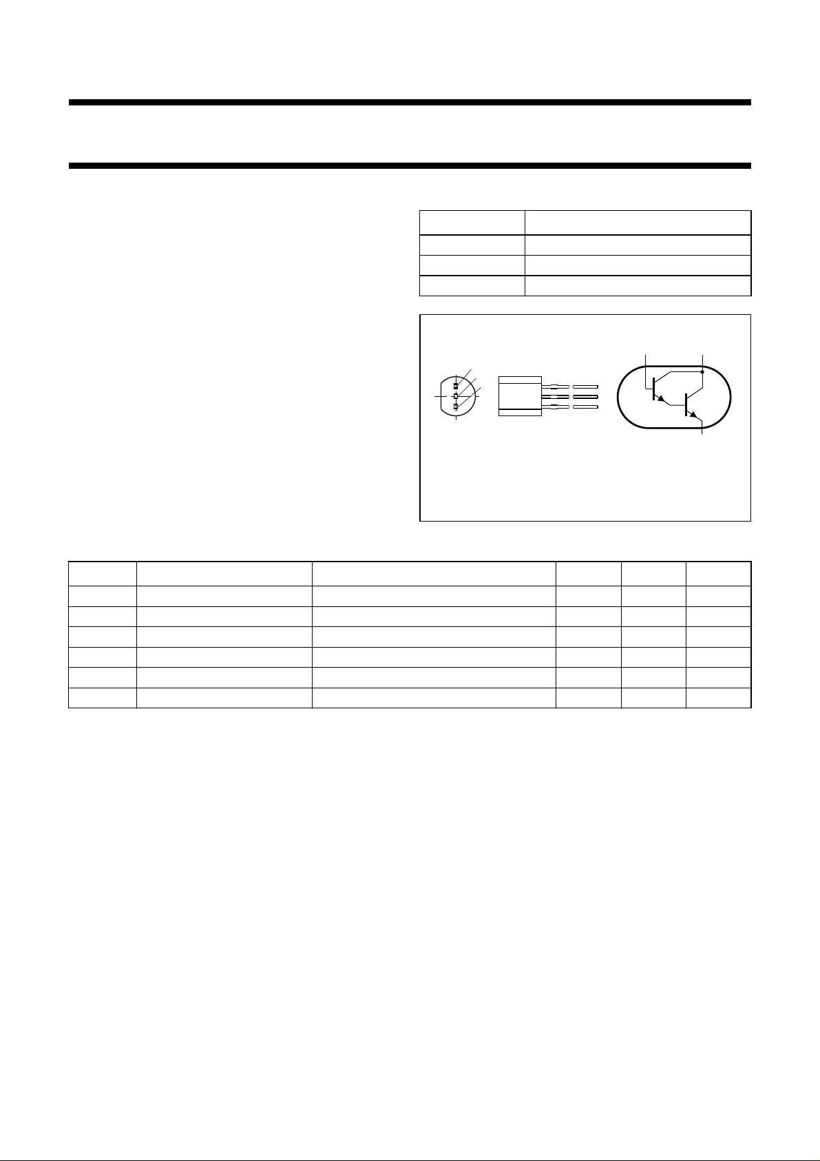
PINNING
PIN DESCRIPTION
1 collector
2 base
3 emitter
APPLICATIONS
• General purpose
• High gain amplification.
DESCRIPTION
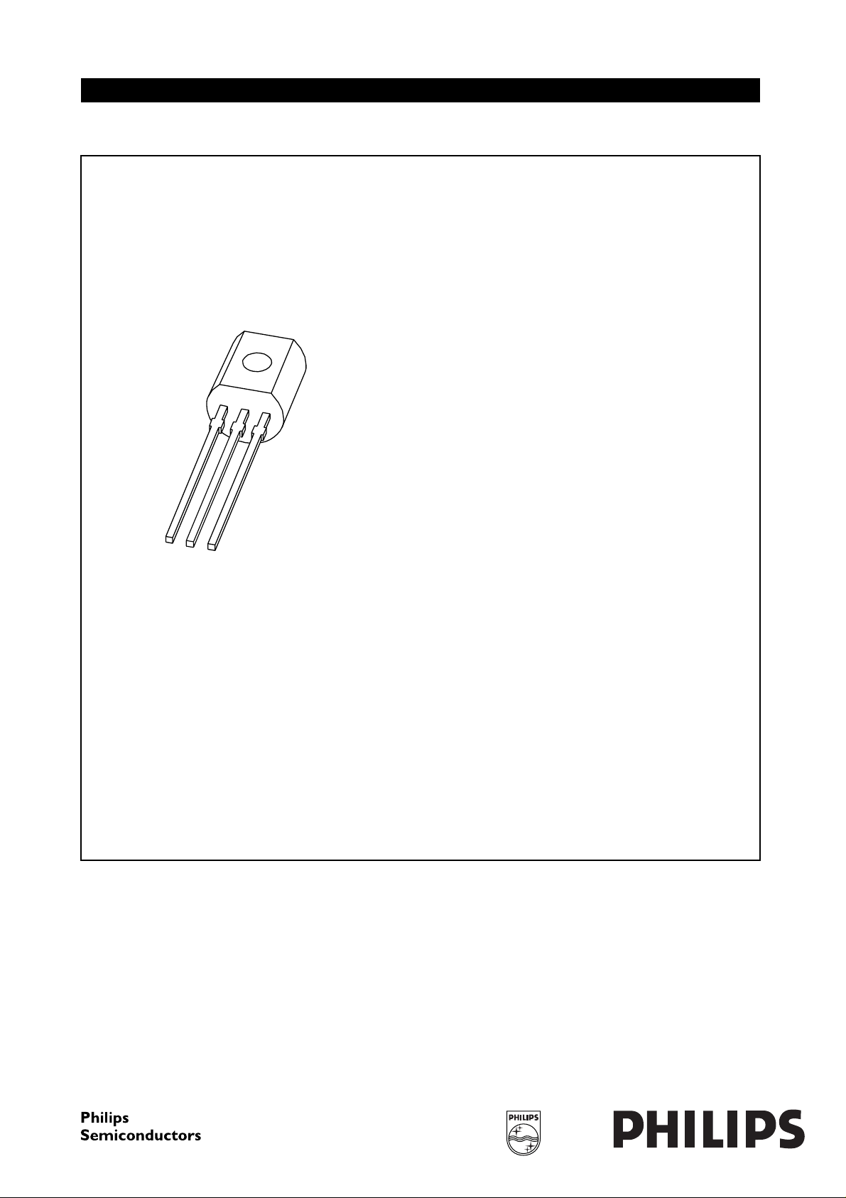
NPN Darlington transistor in a TO-92; SOT54 plastic
package.
handbook, halfpage
1
2
3
2
MAM252
1
TR1
TR2
3
Fig.1 Simplified outline (TO-92; SOT54)
and symbol.
QUICK REFERENCE DATA
SYMBOL PARAMETER CONDITIONS MIN. MAX. UNIT
V
V
I
P
h
f
CBO
CES
C
tot
FE
T
collector-base voltage open emitter − 40 V
collector-emitter voltage VBE=0 − 30 V
collector current − 500 mA
total power dissipation T
≤ 25 °C − 625 mW
amb
DC current gain IC= 10 mA; VCE= 5 V 10000 100000
transition frequency IC= 10 mA; VCE= 5 V; f = 100 MHz 125 − MHz
1997 Jul 04 2
Philips Semiconductors Product specification
NPN Darlington transistor 2N6427
LIMITING VALUES
In accordance with the Absolute Maximum Rating System (IEC 134).
SYMBOL PARAMETER CONDITIONS MIN. MAX. UNIT
V
CBO
V
CES
V
EBO
I
C
I
CM
I
B
P
tot
T
stg
T
j
T
amb
Note
1. Transistor mounted on an FR4 printed-circuit board.
collector-base voltage open emitter − 40 V
collector-emitter voltage VBE=0 − 30 V
emitter-base voltage open collector − 10 V
collector current (DC) − 500 mA
peak collector current − 800 mA
base current (DC) − 200 mA
total power dissipation T
≤ 25 °C; note 1 − 625 mW
amb
storage temperature −65 +150 °C
junction temperature − 150 °C
operating ambient temperature −65 +150 °C
THERMAL CHARACTERISTICS
SYMBOL PARAMETER CONDITIONS VALUE UNIT
R
th j-a
thermal resistance from junction to ambient note 1 200 K/W
Note
1. Transistor mounted on an FR4 printed-circuit board.
CHARACTERISTICS
=25°C unless otherwise specified.
T
amb
SYMBOL PARAMETER CONDITIONS MIN. MAX. UNIT
I
CBO
I
CES
I
EBO
h
FE
V
CEsat
V
BEsat
V
BEon
f
T
collector cut-off current IE= 0; VCB=30V − 100 nA
= 0; VCB=30V; Tj= 150 °C − 10 µA
I
E
collector cut-off current VBE= 0; IB= 0; VCE=30V − 100 nA
emitter cut-off current IC= 0; VEB=10V − 100 nA
DC current gain VCE= 5 V; note 1
= 10 mA 10000 100000
I
C
I
= 100 mA 20000 200000
C
I
= 500 mA 14000 140000
C
collector-emitter saturation voltage IC= 50 mA; IB= 0.5 mA; note 1 − 1.2 V
= 500 mA; IB= 0.5 mA; note 1 − 1.5 V
I
C
base-emitter saturation voltage IC= 500 mA; IB= 0.5 mA; note 1 − 2V
base-emitter on-state voltage IC= 50 mA; VCE=5V − 1.75 V
transition frequency IC= 10 mA; VCE= 5 V; f = 100 MHz 125 − MHz
Note
1. Pulse test: t
≤ 300 µs; δ≤0.02.
p
1997 Jul 04 3
 Loading...