

Philips 2N5087 Datasheet
DISCRETE SEMICONDUCTORS
DATA SH EET
ook, halfpage
M3D186
2N5087
PNP general purpose transistor
Product specification
Supersedes data of September 1994
File under Discrete Semiconductors, SC04
1997 Jul 02
Philips Semiconductors Product specification
PNP general purpose transistor 2N5087
FEATURES
• Low current (max. 100 mA)
• Low voltage (max. 50 V).
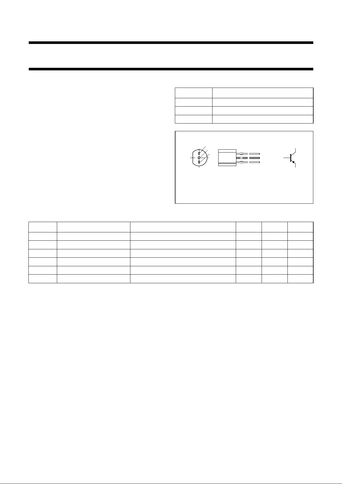
PINNING
PIN DESCRIPTION
1 collector
2 base
APPLICATIONS
3 emitter
• Low noise stages in audio equipment.
DESCRIPTION
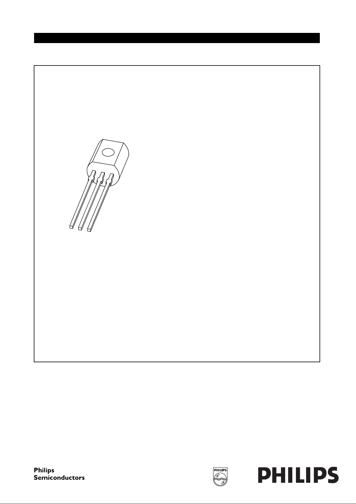
PNP transistor in a TO-92; SOT54 plastic package
NPN complement: 2N5088.
handbook, halfpage
1
2
3
MAM280
1
2
3
Fig.1 Simplified outline (TO-92; SOT54)
and symbol.
QUICK REFERENCE DATA
SYMBOL PARAMETER CONDITIONS MIN. MAX. UNIT
V
V
I
P
h
f
CBO
CEO
CM
tot
FE
T
collector-base voltage open emitter −−50 V
collector-emitter voltage open base −−50 V
peak collector current −−200 mA
total power dissipation T
≤ 25 °C − 500 mW
amb
DC current gain IC= −1 mA; VCE= −5 V 250 −
transition frequency IC= −500 µA; VCE= −5 V; f = 100 MHz 40 − MHz
1997 Jul 02 2
Philips Semiconductors Product specification
PNP general purpose transistor 2N5087
LIMITING VALUES
In accordance with the Absolute Maximum Rating System (IEC 134).
SYMBOL PARAMETER CONDITIONS MIN. MAX. UNIT
V
CBO
V
CEO
V
EBO
I
C
I
CM
I
BM
P
tot
T
stg
T
j
T
amb
Note
1. Transistor mounted on an FR4 printed-circuit board.
collector-base voltage open emitter −−50 V
collector-emitter voltage open base −−50 V
emitter-base voltage open collector −−3V
collector current (DC) −−100 mA
peak collector current −−200 mA
peak base current −−200 mA
total power dissipation T
≤ 25 °C; note 1 − 500 mW
amb
storage temperature −65 +150 °C
junction temperature − 150 °C
operating ambient temperature −65 +150 °C
THERMAL CHARACTERISTICS
SYMBOL PARAMETER CONDITIONS VALUE UNIT
R
th j-a
thermal resistance from junction to ambient note 1 250 K/W
Note
1. Transistor mounted on an FR4 printed-circuit board.
CHARACTERISTICS
=25°C unless otherwise specified.
T
j
SYMBOL PARAMETER CONDITIONS MIN. TYP. MAX. UNIT
I
CBO
I
EBO
h
FE
V
CEsat
collector cut-off current IE= 0; VCB= −10 V −−−10 nA
= 0; VCB= −35 V −−−50 nA
I
E
emitter cut-off current IC= 0; VEB= −3V −−−50 nA
DC current gain IC= −100 µA; VCE= −5 V 250 − 800
I
= −1 mA; VCE= −5 V 250 −−
C
=−10 mA; VCE= −5 V 250 −−
I
C
collector-emitter saturation
IC= −10 mA; IB= −1mA −−−300 mV
voltage
V
BE
C
c
C
e
f
T
F noise figure I
base-emitter voltage IC= −1 mA; VCE= −5V −−−850 mV
collector capacitance IE=ie= 0; VCB= −5 V; f = 100 kHz −−4pF
emitter capacitance IC=ic= 0; VEB= −500 mV; f = 1 MHz − 12 − pF
transition frequency IC= −500 µA; VCE= −5 V; f = 100 MHz 40 −−MHz
= −200 µA; VCE= −5 V; RS=2kΩ;
C
−−3dB
f = 10 Hz to 15.7 kHz
I
=−200 µA; VCE= −5 V; RS=2kΩ;
C
−−4dB
f = 1 kHz; B = 200 Hz
1997 Jul 02 3
 Loading...