

Philips 2N4401 Datasheet
DISCRETE SEMICONDUCTORS
DATA SH EET
ook, halfpage
M3D186
2N4401
NPN switching transistor
Product specification
Supersedes data of 1997 May 07
1999 Apr 23
Philips Semiconductors Product specification
NPN switching transistor 2N4401
FEATURES
• High current (max. 600 mA)
• Low voltage (max. 40 V).
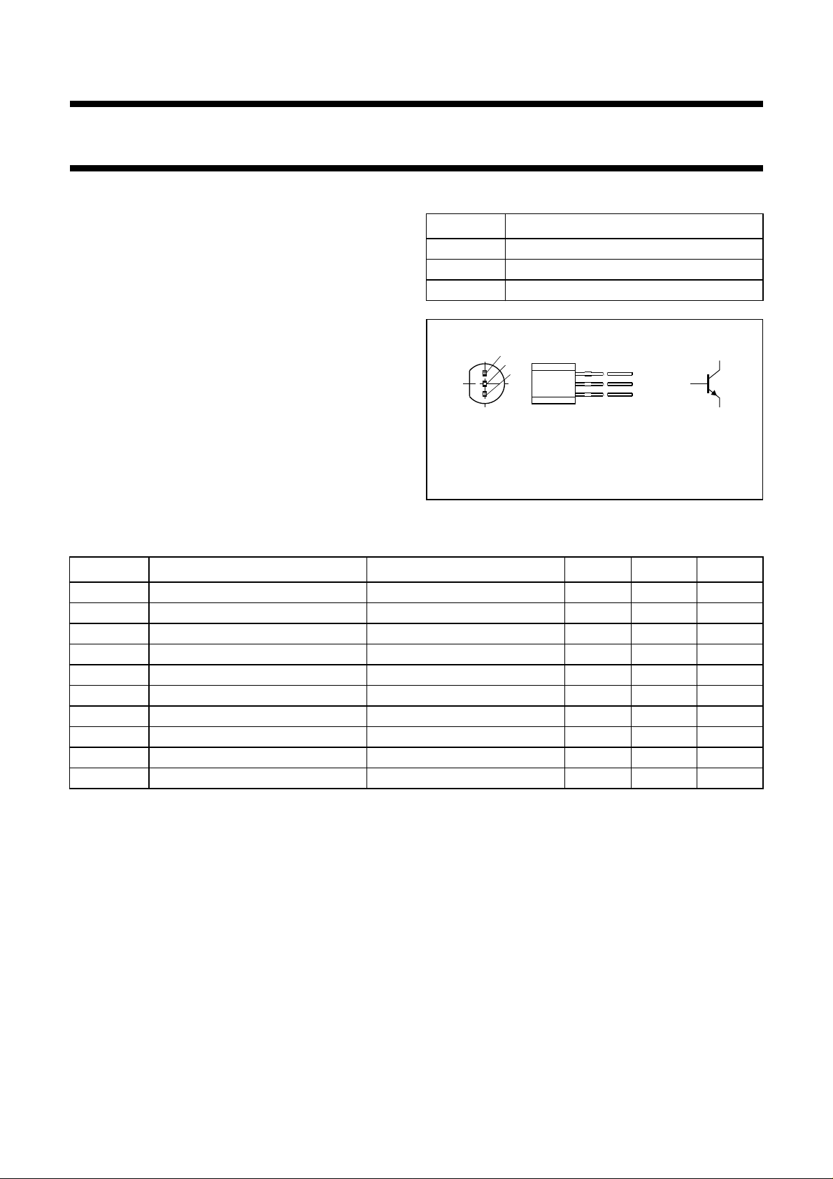
PINNING
PIN DESCRIPTION
1 collector
2 base
APPLICATIONS
3 emitter
• Industrial and consumer switching applications.
DESCRIPTION
NPN switching transistor in a TO-92; SOT54 plastic
handbook, halfpage
1
2
3
2
package. PNP complement: 2N4403.
MAM279
Fig.1 Simplified outline (TO-92; SOT54)
and symbol.
LIMITING VALUES
In accordance with the Absolute Maximum Rating System (IEC 134).
SYMBOL PARAMETER CONDITIONS MIN. MAX. UNIT
V
CBO
V
CEO
V
EBO
I
C
I
CM
I
BM
P
tot
T
stg
T
j
T
amb
collector-base voltage open emitter − 60 V
collector-emitter voltage open base − 40 V
emitter-base voltage open collector − 6V
collector current (DC) − 600 mA
peak collector current − 800 mA
peak base current − 200 mA
total power dissipation T
≤ 25 °C; note 1 − 630 mW
amb
storage temperature −65 +150 °C
junction temperature − 150 °C
operating ambient temperature −65 +150 °C
1
3
Note
1. Transistor mounted on an FR4 printed-circuit board.
1999 Apr 23 2
Philips Semiconductors Product specification
NPN switching transistor 2N4401
THERMAL CHARACTERISTICS
SYMBOL PARAMETER CONDITIONS VALUE UNIT
R
th j-a
Note
1. Transistor mounted on an FR4 printed-circuit board.
CHARACTERISTICS
=25°C unless otherwise specified.
T
j
SYMBOL PARAMETER CONDITIONS MIN. MAX. UNIT
I
CBO
I
EBO
h
FE
V
CEsat
V
BEsat
C
c
C
e
f
T
Switching times (between 10% and 90% levels); see Fig.3
t
on
t
d
t
r
t
off
t
s
t
f
thermal resistance from junction to ambient note 1 200 K/W
collector cut-off current IE= 0; VCB=60V − 50 nA
emitter cut-off current IC= 0; VEB=6V − 50 nA
DC current gain VCE= 1 V; see Fig.2
= 0.1 mA 20 −
I
C
I
= 1 mA 40 −
C
=10mA 80 −
I
C
I
= 150 mA; note 1 100 300
C
I
= 500 mA; VCE= 2 V; note 1 40 −
C
collector-emitter saturation voltage IC= 150 mA; IB= 15 mA; note 1 − 400 mV
I
= 500 mA; IB= 50 mA; note 1 − 750 mV
C
base-emitter saturation voltage IC= 150 mA; IB= 15 mA; note 1 − 950 mV
I
= 500 mA; IB= 50 mA; note 1 − 1.2 V
C
collector capacitance IE=ie= 0; VCB=5V; f=1MHz − 6.5 pF
emitter capacitance IC=ic= 0; VEB= 500 mV; f = 1 MHz − 30 pF
transition frequency IC= 20 mA; VCE= 10 V; f = 100 MHz 250 − MHz
turn-on time I
delay time − 15 ns
= 150 mA; I
Con
I
= −15 mA
Boff
Bon
= 15 mA;
− 35 ns
rise time − 20 ns
turn-off time − 250 ns
storage time − 200 ns
fall time − 60 ns
Note
1. Pulse test: t
≤ 300 µs; δ≤0.02.
p
1999 Apr 23 3
 Loading...