

Philips 2N4427, 2N3866 Datasheet

DISCRETE SEMICONDUCTORS
DATA SH EET
2N3866; 2N4427
Silicon planar epitaxial
overlay transistors
Product specification
Supersedes data of August 1986
File under Discrete Semiconductors, SC08a
1995 Oct 27
Philips Semiconductors Product specification
Silicon planar epitaxial
overlay transistors
DESCRIPTION
NPN overlay transistors in TO-39 metal packages with the
collector connected to the case. The devices are primarily
intended for class-A, B or C amplifiers, frequency multiplier
and oscillator circuits.
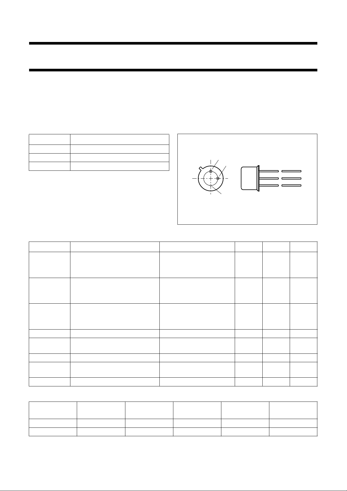
PINNING - TO-39/1
PIN DESCRIPTION
1 emitter
2 base
3 collector
2N3866; 2N4427
APPLICATIONS
• The transistors are intended for use in output, driver or
pre-driver stages in VHF and UHF equipment.
handbook, halfpage
1
2
3
Fig.1 Simplified outline.
MBB199
QUICK REFERENCE DATA
SYMBOL PARAMETER CONDITIONS MIN. MAX. UNIT
V
CER
collector-emitter voltage RBE=10Ω
2N3866 − 55 V
2N4427 − 40 V
V
CEO
collector-emitter voltage open base
2N3866 − 30 V
2N4427 − 20 V
V
EBO
emitter-base voltage open collector
2N3866 − 3.5 V
2N4427 − 2.0 V
I
C
I
C(AV)
collector current (DC) − 0.4 A
average collector current measured over any 20 ms
− 0.4 A
period
P
tot
f
T
total power dissipation up to Tmb=25°C − 3.5 W
transition frequency IC= 50 mA; VCE=15V;
500 − MHz
f = 200 MHz
T
j
junction temperature − 200 °C
RF performance
TYPE NUMBER
f
(MHz)
V
(V)
CE
P
(W)
o
G
p
(dB)
2N3866 400 28 1 >10 >45
2N4427 175 12 1 >10 >50
1995 Oct 27 2
η
(%)

Philips Semiconductors Product specification
Silicon planar epitaxial
2N3866; 2N4427
overlay transistors
LIMITING VALUES
In accordance with the Absolute Maximum Rating System (IEC 134).
SYMBOL PARAMETER CONDITIONS MIN. MAX. UNIT
V
CBO
V
CER
V
CEO
V
EBO
I
C
I
C(AV)
I
CM
P
tot
T
stg
T
j
collector-base voltage open emitter
2N3866 − 55 V
2N4427 − 40 V
collector-emitter voltage RBE=10Ω
2N3866 − 55 V
2N4427 − 40 V
collector-emitter voltage open base
2N3866 − 30 V
2N4427 − 20 V
emitter-base voltage open collector
2N3866 − 3.5 V
2N4427 − 2.0 V
collector current (DC) − 0.4 A
average collector current measured over any 20 ms
− 0.4 A
period
collector current peak value − 0.4 A
total power dissipation up to Tmb=25°C − 3.5 W
storage temperature −65 +200 °C
junction temperature − 200 °C
THERMAL CHARACTERISTICS
SYMBOL PARAMETER CONDITIONS VALUE UNIT
R
th j-a
thermal resistance from junction
200 K/W
to ambient in free air
R
th j-mb
thermal resistance from junction
50 K/W
to mounting base
R
th mb-h
thermal resistance from
mounting base to heatsink
note 1 1.0 K/W
note 2 2.5 K/W
Notes
1. Mounted with top clamping washer 56218.
2. Mounted with top clamping washer 56218 and a boron nitride washer for electrical insulation.
1995 Oct 27 3
 Loading...