

Philips 2N1711 Datasheet
DISCRETE SEMICONDUCTORS
DATA SH EET
ook, halfpage
M3D111
2N1711
NPN medium power transistor
Product specification
Supersedes data of September 1994
File under Discrete Semiconductors, SC04
1997 May 28
Philips Semiconductors Product specification
NPN medium power transistor 2N1711
FEATURES
• High current (max. 500 mA)
• Low voltage (max. 50 V).
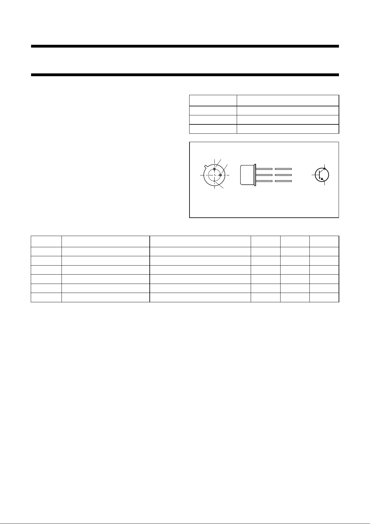
PINNING
PIN DESCRIPTION
1 emitter
2 base
APPLICATIONS
3 collector, connected to case
• DC and wideband amplifiers.
DESCRIPTION
handbook, halfpage
1
2
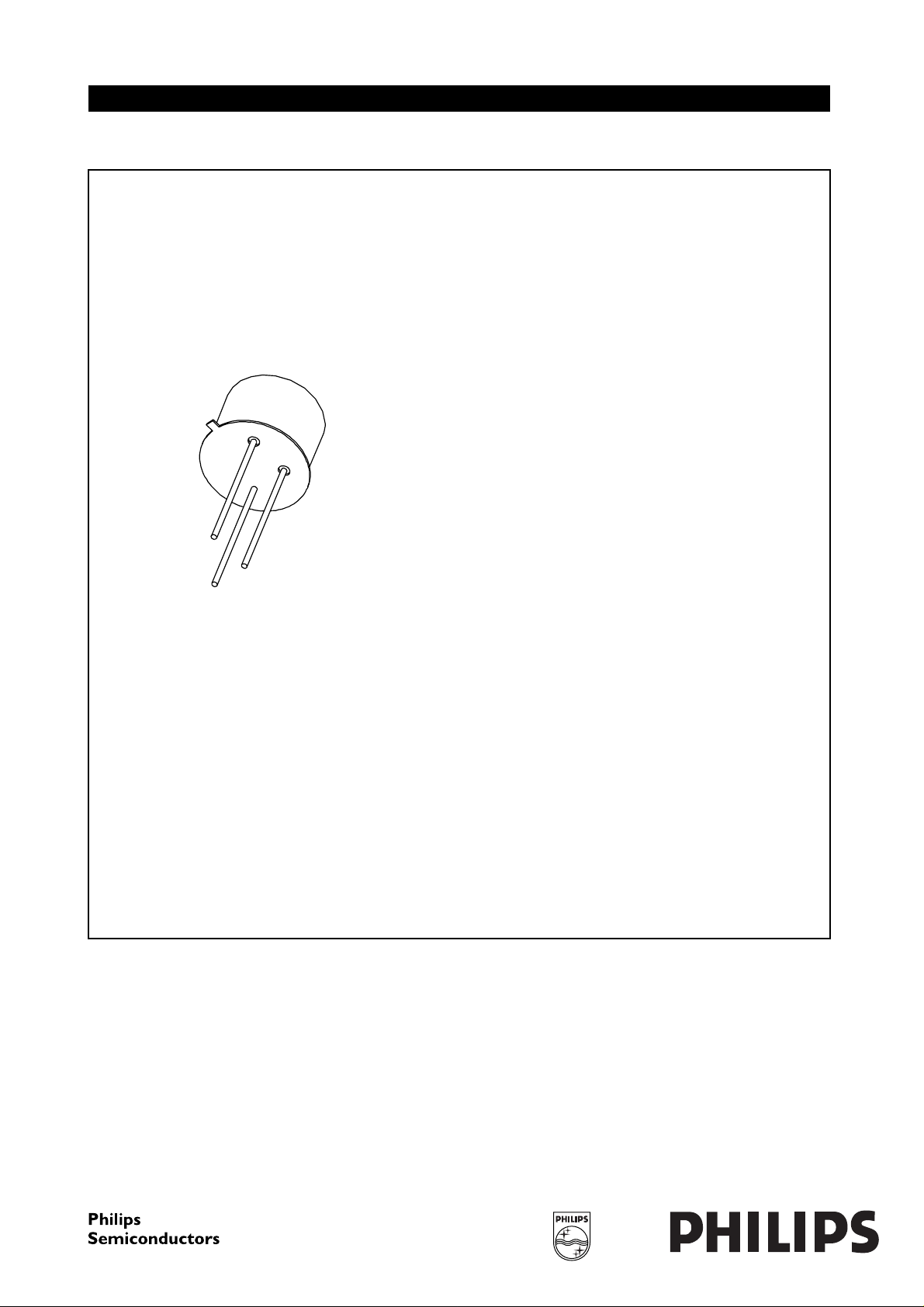
NPN medium power transistor in a TO-39 metal package.
2
3
MAM317
Fig.1 Simplified outline (TO-39) and symbol.
QUICK REFERENCE DATA
SYMBOL PARAMETER CONDITIONS MIN. MAX. UNIT
V
CBO
V
CEO
I
CM
P
tot
h
FE
f
T
collector-base voltage open emitter − 75 V
collector-emitter voltage open base − 50 V
peak collector current − 1A
total power dissipation T
≤ 25 °C − 0.8 W
amb
DC current gain IC= 150 mA; VCE= 10 V 100 300
transition frequency IC= 50 mA; VCE= 10 V; f = 100 MHz 70 − MHz
3
1
1997 May 28 2
Philips Semiconductors Product specification
NPN medium power transistor 2N1711
LIMITING VALUES
In accordance with the Absolute Maximum Rating System (IEC 134).
SYMBOL PARAMETER CONDITIONS MIN. MAX. UNIT
V
CBO
V
CEO
V
EBO
I
C
I
CM
I
BM
P
tot
T
stg
T
j
T
amb
collector-base voltage open emitter − 75 V
collector-emitter voltage open base − 50 V
emitter-base voltage open collector − 7V
collector current (DC) − 500 mA
peak collector current − 1A
peak base current − 200 mA
total power dissipation T
≤ 25 °C − 0.8 W
amb
T
≤ 100 °C − 1.7 W
case
T
≤ 25 °C − 3W
case
storage temperature −65 +150 °C
junction temperature − 200 °C
operating ambient temperature −65 +150 °C
THERMAL CHARACTERISTICS
SYMBOL PARAMETER CONDITIONS VALUE UNIT
R
R
th j-a
th j-c
thermal resistance from junction to ambient in free air 219 K/W
thermal resistance from junction to case 58.3 K/W
CHARACTERISTICS
T
=25°C unless otherwise specified.
amb
SYMBOL PARAMETER CONDITIONS MIN. MAX. UNIT
I
CBO
I
EBO
h
FE
V
CEsat
V
BEsat
f
T
C
c
C
e
collector cut-off current IE= 0; VCB=60V − 10 nA
I
= 0; VCB=60V; T
E
= 150 °C − 10 µA
amb
emitter cut-off current IC= 0; VEB=5V − 5nA
DC current gain IC=10µA; VCE=10V 20 −
= 0.1 mA; VCE=10V 35 −
I
C
= 10 mA; VCE= 10 V; note 1 75 −
I
C
I
= 10 mA; VCE=10V; T
C
I
= 150 mA; VCE= 10 V; note 1 100 300
C
I
= 500 mA; VCE= 10 V; note 1 40 −
C
= −55 °C35 −
amb
collector-emitter saturation voltage IC= 150 mA; IB= 15 mA; note 1 − 500 mV
base-emitter saturation voltage IC= 150 mA; IB= 15 mA; note 1 − 1.3 V
transition frequency IC= 50 mA; VCE= 10 V; f = 100 MHz 70 − MHz
collector capacitance IE=ie= 0; VCB= 10 V; f = 1 MHz − 25 pF
emitter capacitance IC=ic= 0; VEB= 0.5 V; f = 1 MHz − 80 pF
Note
1. Pulse test: t
≤ 300 µs; δ≤0.02.
p
1997 May 28 3
 Loading...