

Philips 2moa3 DATASHEETS

TM
HT2 MOA3 S20
HITAG
Revision 1.1
2 Chip Module
August 1997Preliminary Specification

Specifications of the HT2 MOA3 S20 Rev. 1.1 1997-08-19
Table of Contents
1 Definitions.............................................................................................................................. 3
1.1 Objective of the Specifications..................................................................................................................... 3
1.2 Definition of the Chip Module..................................................................................................................... 3
1.3 Use of the Modules......................................................................................................................................3
2 Specifications.........................................................................................................................4
2.1 Mechanical Properties ................................................................................................................................. 4
2.2 Materials .....................................................................................................................................................4
2.3 Temperature Range .....................................................................................................................................4
2.4 Storage Conditions ...................................................................................................................................... 5
2.5 Delivery Conditions.....................................................................................................................................5
2.6 Electrical Specifications............................................................................................................................... 6
3 Drawing of the Chip Module HT2 MOA3 S20 ..................................................................... 7
3.1 Drawing of the Reel.....................................................................................................................................7
3.2 Module outline suggestion........................................................................................................................... 8
3.3 Splicing Specification..................................................................................................................................9
4 Coil Specifications................................................................................................................ 10
5 Functional Description of HITAG 2 ................................................................................... 12
5.1 Memory Organization........................................................................................................ ........................ 12
5.2 Operation Modes and Configuration.......................................................................................................... 13
5.2.1 Modes of Operation............................................................................................................................13
5.2.2 Status Flow ........................................................................................................................................14
5.2.3 Configuration.....................................................................................................................................15
5.3 Configuration of Delivered HITAG 2 Transponders................................................................................... 16
5.4 Definition of Passwords and Keys..............................................................................................................17
6 Quality Inspection ............................................................................................................... 18
7 Characterisation and Test of the Final Transponder.........................................................19
7.1 Characterisation of the Transponder.......................................................................................................... 19
7.2 Final Test of the Transponder.................................................................................................................... 19
8 Ordering Information..........................................................................................................20
HITAGTM is a trademark of Philips Electronics N.V.
Ht2moa3.doc/HS Page 2 of 22

Specifications of the HT2 MOA3 S20 Rev. 1.1 1997-08-19
1 Definitions
1.1 Objective of the Specifications
This specification lists the parameters to be fulfilled by the HITAG 2 chip module
HT2 MOA3 S20 for contactless smart cards or similar transponders (as e.g. discs).
1.2 Definition of the Chip Module
A chip module is an electronically packaged chip covered with a globe top cap. The
HT2 MOA3 S20 is above all used as card module, i.e. for further lamination into contactless
smart cards according to ISO 10536.1.
So the HIT AG 2 chip module HT2 MOA3 S20 is best suited for customers that do not want t o
spend time with micro assembly and therefore start - e.g. ISO card production - with the
HITAG 2 chip module.
1.3 Use of the Modules
The HITAG 2 modules are designed to be connected to a coil and then to be further processed by
packaging into a transponder (e.g. lamination into an ISO smart card). Specific processing
information for the coil-module connection and packaging is given in the specification.
For production of contactless chip cards it is recommended to prepunch card foils to create a
recess for the chip module in the card body.
Ht2moa3.doc/HS Page 3 of 22

Specifications of the HT2 MOA3 S20 Rev. 1.1 1997-08-19
2 Specifications
2.1 Mechanical Properties
Width
(Proposed Punching Outline)
Length
(Proposed Punching Outline)
Overall Thickness 0.45 mm ± 0.03 mm
Film Thickness 0.16 mm ± 0.005 mm
Bondpad Size for
Transponder Coil / Module
Interconnection
7.55 mm
11.75 mm see also drawing in chapter 3
1.9 x 3.5 mm Suitable for Welding/Soldering/
Conductive Gluing
2.2 Materials
Tape 110 µm Glass epoxy
Copper Plating 35 µm ED copper
Bond Plating Ni / Au Suitable for Al and Au wire
bonding
Backside Plating Ni / Au
Glob Top Filled Epoxy Thermal curing
2.3 Temperature Range
Operating -25°C to +85°C For packed transponder,
depending on type of package
Processing 150°C for 30 minutes at a standard lamination
pressure for contactless smart
card plastic materials (e.g. PVC,
PET, ...)
Welding Parameters max. 25 ms @ 500 °C on bond pads
Soldering Parameters max. 3 s @ 390 °C on bond pads
Ht2moa3.doc/HS Page 4 of 22

Specifications of the HT2 MOA3 S20 Rev. 1.1 1997-08-19
2.4 Storage Conditions
Temperature 15 - 30 °C
Relative Humidity 40 - 70 %
Duration 1 year
2.5 Delivery Conditions
Delivery Identification Date of ready for shipment, reel numbers, total quantity of good
modules with the detail of good modules per reel, order number,
product type, no supplier identification on reels, bags and boxes.
Types of Delivery Chip modules on reel
approx. 15.000 to 20.000
pcs. per reel,
tape width super 35 mm,
pitch 9,5 mm, 2 rows
single chip modules (bulk goods)
Packing and Transport According to documentation
"Packing Method Modules (reel)"
"Packing Method Modules (singulated)"
Bad Module Marking All bad modules (mechanical and
electrical faults) must be punched by
reject hole for customer
Bad positions (reel): <20%
Splicing Specifications Tape material: adhes. tape 15,5 +/- 0,7
mm, thermal resistance at
<190°C by < 100 cN tractive power and
< 30 sec. duration.
Labeling Identification label on the reel and on
carton bag:
- Product type
- Number of the reel
- Total number of positions
- Number of good positions
- Date of sealing (to be checked)
- Two batches per reel only
- Batch number indication (only coded,
to be checked)
500 pcs . per bag
Order-No. 3322 845 04881
see drawings chapter 3
see drawings chapter 3
Ht2moa3.doc/HS Page 5 of 22

Specifications of the HT2 MOA3 S20 Rev. 1.1 1997-08-19
2.6 Electrical Specifications
Symbol min typ max Comment / Conditions
Absolute Maximum Ratings
Junction Temperature T
Input Peak Current I
J
INpeak
-55°C 140°C
30 mA
Latch up Current 100 mA MIL-STD 883D, Method 3023
ESD 2 kV MIL-STD 883D, Method 3015.7,
Human Body
Operating Range
Temperature T
Input Read Only Threshold
Voltage
Input Threshold Voltage
Input Read Voltage
Input Write Voltage
1)
3)
1)
3)
1)
3)
1)
3)
V
V
V
V
A
IN,RO
IN,TH
IN,RD
IN,WR
-40°C 85°C
2,8 Vp3,9 Vpstart modulation in read only
3,1 Vp4,2 Vpstart modulation after SETCC
3,5 Vp4,5 Vpread E²PROM
3,7 Vp4,7 Vpwrite E²PROM
R
ThJunctionAmbient
= 30 mA
I
INpeak
modes
≤ 30 K/W @
Demodulator
Range
3)
V
DEM_R
2,0 V
p
4,0 VpV
- V
INHigh
T0=8 µs, T
INLow
MOD
@ V
=6*T
INHigh
0
= 5,0 V
2)
Modulator
R_MOD linear
R_MOD nonlinear
3)
3)
Resonance Capacitor
3)
R
MODL
R
MODNL
4,5 kΩV
3,6 kΩV
INLow
INLow
≤ 2,0 V
≥ 2,0 V
p
p
p
C
ResInit
189 pF 210 pF 231 pF VIN = 4,0 V
EEPROM
Write Current
Read Current
4)
4)
I
W
I
R
25 µA VDD = 2,8 V
9 µA VDD = 2,8 V
Data Retention Years 10 @ 55°C
Write Endurance Cycles 100.000
1)
2)
3)
4)
tested on silicon level
V
IN
INHigh
INLow
MOD
= V
V
V
T
@ Ri = 10
IN1
− V
... voltage between connection pads
IN2
input voltage before modulation
input voltage during modulation
duration of the modulation
resistance of measurement equipment
Ω
k
p
Ht2moa3.doc/HS Page 6 of 22
Specifications of the HT2 MOA3 S20 Rev. 1.1 1997-08-19
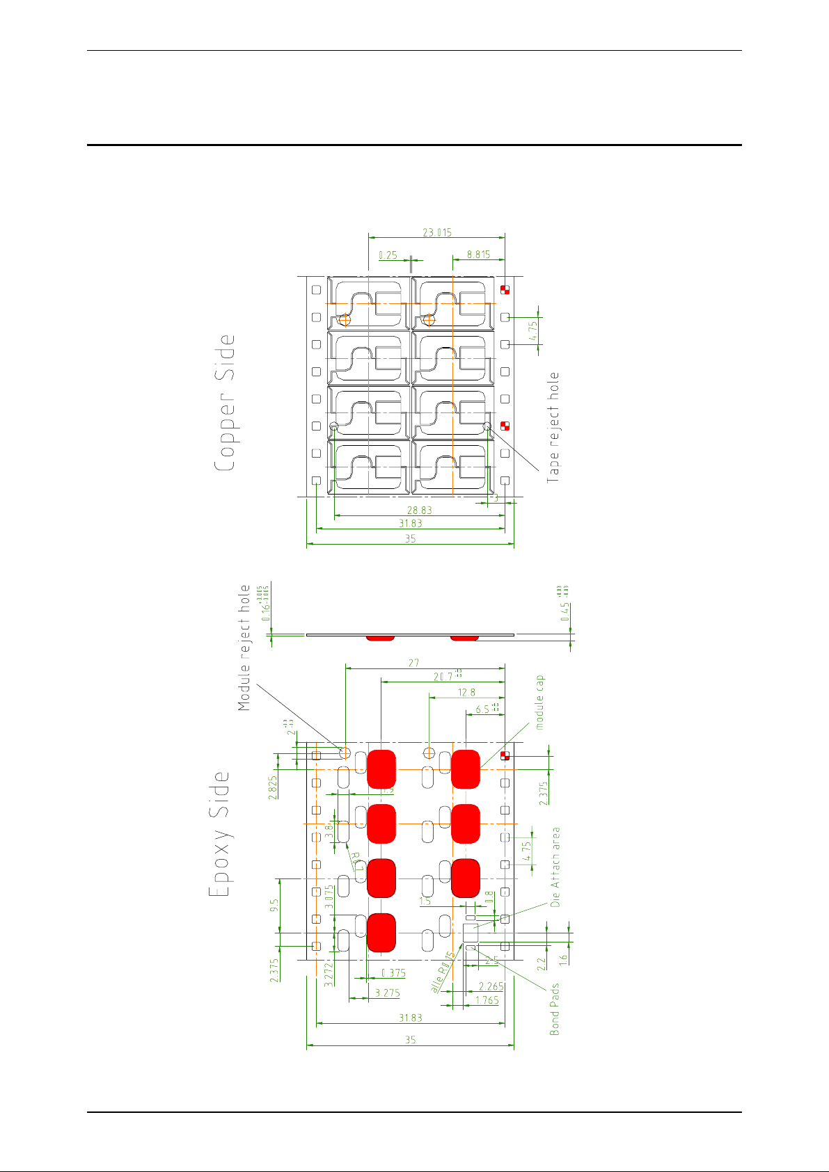
3 Drawing of the Chip Module HT2 MOA3 S20
3.1 Drawing of the Reel
Ht2moa3.doc/HS Page 7 of 22
 Loading...