

Philips 298P4QJEB/75, 298P4QJEB/69, 298P4QJEB/27, 298P4QJEB/57, 298X4QJAB/00 Service Manual
...
29ƎLCD Color Monitor Chassis: Meridian 3
Service
Service
Service
Description
Page
Table of Contents.........................................………….1
Revision List………….................................................2
Important Safety Notice…………................................3
1. Monitor Specifications….........................................5
2. LCD Monitor Description….....................................7
3. Operation Instructions….........................................8
3.1General Instructions…………………………….…...8
3.2 Control Buttons…………..…………………….…8
3.3 OSD Menu………………….................................9
4. Input/output Specification............................……10
4.1 Input Signal Connector.................................……10
4.2 Resolution & Preset Modes.................................11
4.3 Pixel Defect Policy…………………………………12
4.4 Failure Mode of Panel………………………….....14
5. Block Diagram………………………….................15
5.1 Scaler Board....................................………….....15
5.2 Power Board…….................................…...........16
6. Schematic Diagram.............................................. 17
6.1 Scaler Board…………………….…………………17
Description
Page
6.2 Power Board.................................................…...32
6.3 Key Board…….……………………………….……34
6.4 Head Phone Jack Board…….………………35
7. PCB Layout……………………………..…………...36
7.1 Scaler Board…………………………………...…..36
7.2 Power Board……………...………………..………37
7.3 Key Board…….……….……………………………38
7.4 Head Phone Jack Board…….………………38
8. Wiring Diagram………………………………….…..39
9. Scaler Board Overview………….………………....40
10. Mechanical Instructions…………………..……....41
1 1. Repair Flow Chart…….……………………………45
12. ISP Instructions...…............................................49
13. DDC Instructions….............................................55
14. White Balance, Luminance Adjustment…...........89
15. Monitor Exploded View…....................................91
16. Recommended & Spare Part s List...…................93
17. General Product Specification……… ….…..…….97
SAFETY NOTICE
ANY PERSON ATTEMPTING TO SERVICE THIS CHASSIS MUST FAMILIARIZE HIMSELF WITH THE
CHASSIS AND BE AWARE OF THE NECESSARY SAFETY PRECAUTIONS TO BE USED WHE N
SERVICING ELECTRONIC EQUIPMENT CONTAINING HIGH VOLTAGES.
CAUTION: USE A SEPARATE ISOLATION TRANSFOMER FOR THIS UNIT WHEN SERVICING
REFER TO BACK COVER FOR IMPORTANT SAFETY GUIDELINES
Copyright 2013 Philips Consumer Lifestyle Subject to modification ƻK Oct. 18.2013
298P4QJEB/00
298P4QJEB/69
298P4QJEB/93
298P4QJEB/94
298P4QJEB/75
298P4QJEB/27
298P4QJEB/57
298X4QJAB/00
298X4QJAB/93
298X4QJAB/27
298X4QJAB/96
298X4QJAB/75
298X4QJAB/69
298X4QJAB/11
298P4QJEB/96
298P4QAJEB/93
298P4QJEB/01

!
!
Meridian 3
2
Revision List
Version Release Date Revision History
A00 Feb.7, 2013 Initial release, Draft Version
A01 Feb.22, 2013 Add CTN model 298P4QJEB/69 & 298P4QJEB/93
A02 Mar.1, 2013 Add CTN model 298P4QJEB/94
A03 Mar.8, 2013 Add CTN model 298P4QJEB/75 & 298X4QJAB/00
A04 Apr.3, 2013 Add CTN model 298X4QJAB/93
A05 Apr.12, 2013 Add CTN model 298P4QJEB/27 & 298X4QJAB/27
A06 Apr.19, 2013 Add CTN model 298X4QJAB/96
A07 May.24, 2013 Add CTN model 298X4QJAB/75
A08 Jun.14, 2013 Add CTN model 298X4QJAB/69
A09 Jul.19, 2013 Add CTN model 298P4QJEB/57
A10 Aug. 9, 2013 Add CTN model 298P4QJEB/96
A1 1 Sep. 6, 2013 Add CTN model 298X4QJAB/11
A12 Sep. 27, 2013 Add CTN model 298P4QAJEB/93
A13 Oct. 18, 2013 Add CTN model 298P4QJEB/01

3
Meridian 3
Important Safety Notice
This electronic user guide is intended for anyone who uses the Philips monitor. Take time to read this user manual
before you use your monitor. It contains important information and notes regarding operating your monitor. The
Philips guarantee applies provided the product is handled properly for its intended use, in accordance with its
operating instructions and upon presentation of the o riginal invoice or cash receipt, indicatin g the date of p urchase,
dealers name and model and production number of the product.
Warnings
Use of controls, adjustments or procedures other than those specified in this document ation may result in exposure
to shock, electrical hazards and/or mechanical hazards. Read and follow these instructions when connecting and
using your computer monitor.
Operation
y Keep the monitor out of direct sunlight and away from stoves or any other heat source.
y Remove any object that could fall into ventilation holes or prevent proper cooling of the monitor’s electronics.
y Do not block the ventilation holes on the cabinet.
y When positioning the monitor , make sure the power plug and outlet are easily accessible.
y If turning off the monitor by detaching the power cable or DC power cord, wait for 6 seconds before attaching
the power cable or DC power cord for normal operation.
y Please use approved power cord provided by Philips all the time. If your power cord is missing, please contact
with your local service center. (Please refer to Customer Care Consumer Information Center)
y • Do not subject the monitor to severe vibration or high impact conditions during operation.
y • Do not knock or drop the monitor during operation or transportation.
Maintenance
y To protect your monitor from possible damage, do not put excessive pressure on the LCD panel. When moving
your monitor, grasp the frame to lift; do not lift the monitor by placing your hand or fingers on the LCD panel.
y Unplug the monitor if you are not going to use it for an extensive period of time.
y Unplug the monitor if you need to clean it with a slightly damp cloth. The screen may be wiped with a dry cloth
when the power is off. However , never use organic sol vent, such as, alcoh ol, or ammonia-ba sed liquids to clean
your monitor.
y To avoid the risk of shock or permanent damage to the set, do not expose the monitor to dust, rain, water, or
excessive moisture environment.
y If your monitor gets wet, wipe it with dry cloth as soon as possible.
y If foreign substance or water gets in your monitor, please turn the power off immediately and disconnect the
power cord. Then, remove the foreign substance or water, and send it to the maintenance center.
y Do not store or use the monitor in locations exposed to heat, direct sunlight or extreme cold.
y In order to maintain the best performance of your monitor and use it for a longer lifetime, please use the monitor
in a location that falls within the following temperature and humidity ranges.
¾ Temperature: 0-40°C 32-95°F
¾ Humidity: 20-80% RH

!
!
Meridian 3
4
y IMPORTANT: Always activate a moving screen saver program when you leave your monitor unattended.
Always activate a periodic screen refresh application if your monitor will display unchanging static content.
Uninterrupted display of still or static images over an extended period may cause “burn in”, also known a s
“after-imaging” or “ghost imaging”, on your screen. “Burn-in”, “after-imaging”, or “ghost imaging” is a
well-known phenomenon in LCD panel technology. In most cases, the “burned in” or “after-imaging” or “ghost
imaging” will disappear gradually over a period of time after the power has bee n switched off.
Warning
Severe” burn-in” or “after-image” or “ghost image” symptoms will not disappear and cannot be repaired. The
damage mentioned above is not covered under your warranty.
Service
y The casing cover should be opened only by qualified service personnel.
y If there is any need for any document for repair or integration, please contact with your local service center.
(Please refer to the chapter of “Consumer Information Center”)
y For transportation information, please refer to “Technical Specifications”.
y Do not leave your monitor in a car/trunk under direct sun light.
Note
Consult a service technician if the monitor does not operate normally, or you are not sure what procedure to take
when the operating instructions given in this manual have been followed.
5
Meridian 3
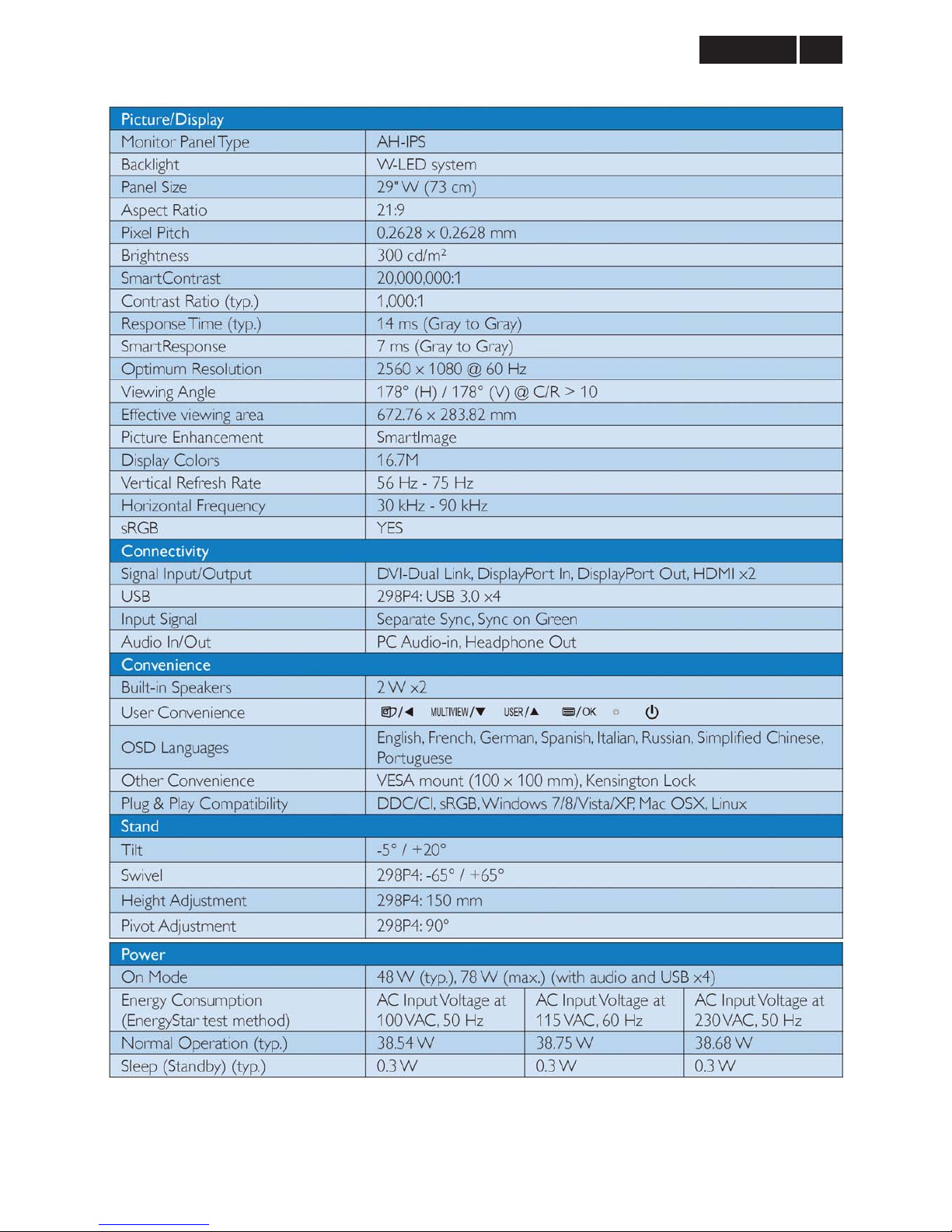
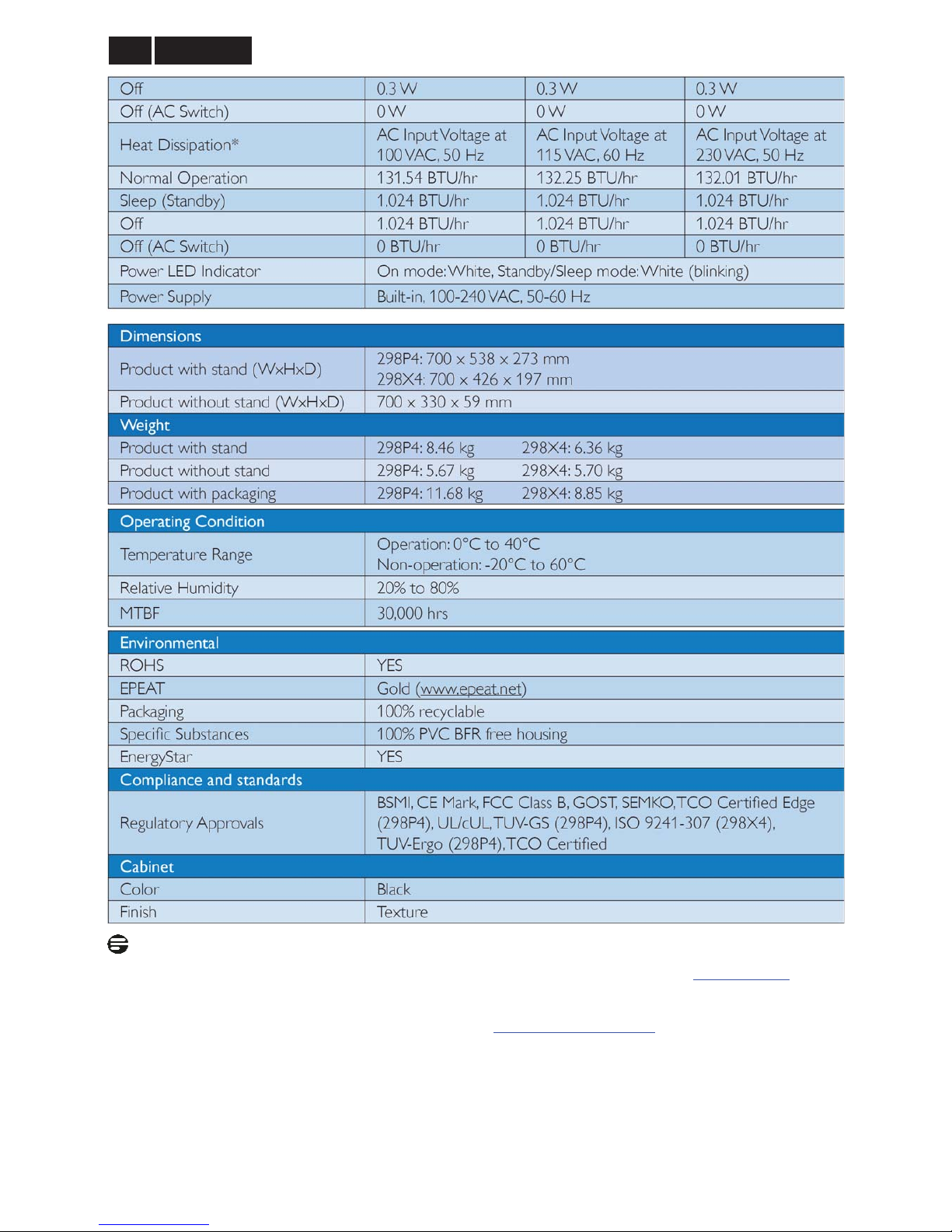
1. Monitor Specifications
!
!
Meridian 3
6
Note:
1. EPEAT Gold or Silver is valid only where Philips registers the product. Please visit www.epeat.net
for
registration status in your country.
2. This data is subject to change without notice. Go to www.philips.com/support
to download the latest
version of leaflet.
7
Meridian 3
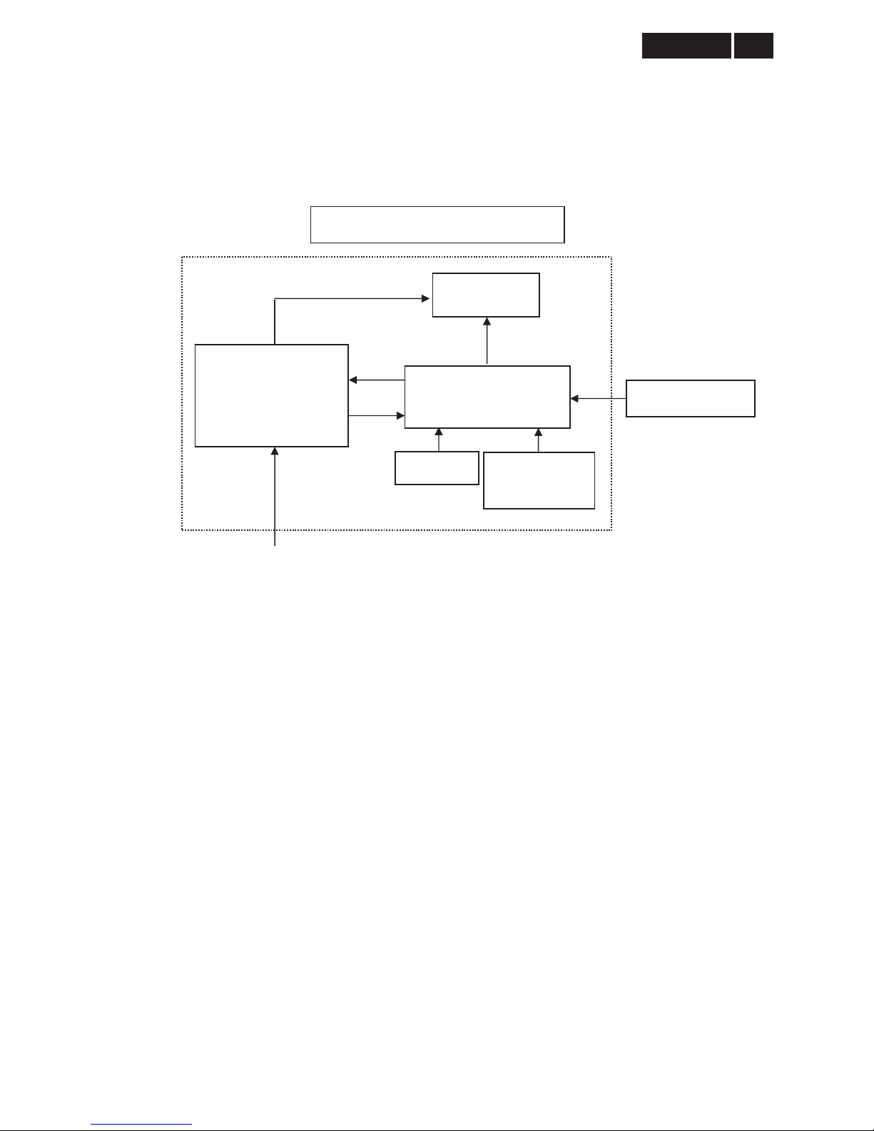
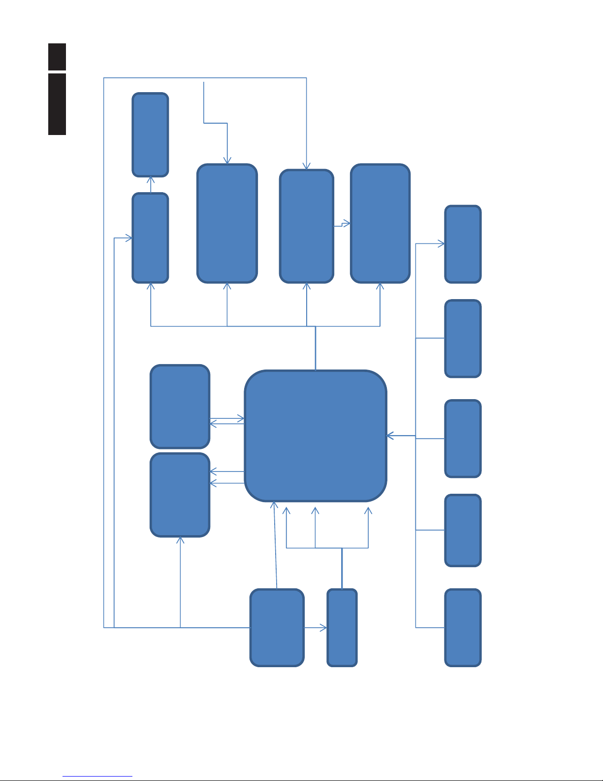
2. LCD Monitor Description
The LCD monitor will contain a scaler board, a power board, a head phone jack board and a key board. Th e scaler
board houses the flat panel control logic, brightness control logic and DDC.
The power board will provide AC to DC inverter voltage to drive the backlight of panel and the scaler board chips
each voltage.
Monitor Block Diagram
LED Panel
Scaler Board
(Include: Audio)
HOST Computer
LED Drive
Key Board
Video signal, DDC
AC IN
100 ~ 240 V
HEAD PHONE
JACK Board
Power Board

!
!
Meridian 3
8
3. Operating Instructions
3.1 General Instructions
Press the power button to turn the monitor on or off.
The other control knobs are located at front panel of
the monitor. By changing these setting, the picture
can be adjusted to your personal preference.
γThe power cord should be connected.
γ Press the power button to turn on the monitor.
The power indicator will light up.
3.2 Control Buttons
Operating the Monitor
Connecting to your PC

9
Meridian 3
3.3 OSD Menu
On-screen Display (OSD) is feature in all Philips LCD
monitors. It allows an end user to adjust screen
performance or select functions of the monitors directly
through an on-screen instruction window. A user
friendly on screen display interface is shown as below:
Basic and simple instruction on the control
keys
In the OSD shown above, you can press źŸ buttons
on the front bezel of the monitor to move the cursor,
and press OK button to confirm the choice or change.
The OSD Menu
Below is an overall view of the structure of the
On-Screen Display. You can use this as a reference
when you want to work your way around the different
adjustments later on.

!
!
Meridian 3
10
4. Input/ Output Specification
4.1 Input Signal Connector
DVI Connector
Pin No. Signal Name
1 T.M.D.S. data22 T.M.D.S. data2+
3 T.M.D.S. data2 shield
4 No Connect
5 No Connect
6 DDC clock
7 DDC data
8 No Connect
9 T.M.D.S. data110 T.M.D.S. data1+
1 1 T.M.D.S. data1 shield
12 No Connect
13 No Connect
14 +5V Power
15 Ground (for +5V)
16 Hot plug detect
17 T.M.D.S. data018 T.M.D.S. data0+
19 T.M.D.S. data0 shield
20 No Connect
21 No Connect
22 T.M.D.S clock shield
23 T.M.D.S. clock+
24 T.M.D.S. clock-
DP Connector
Pin No. Signal Name
1
ML_Lane 3(n)
2
Ground
3
ML_Lane 3(p)
4
ML_Lane 2(n)
5
Ground
6
ML_Lane 2(p)
7
ML_Lane 1(n)
8
Ground
9
ML_Lane 1(p)
10
ML_Lane 0(n)
11
Ground
12
ML_Lane 0(p)
13
Ground
14
Ground
15
AUX_CH (P)
16
Ground
17
AUX_CH (N)
18
Hot Plug Detect
19
Return DP_PWR
20
DP_PWR
HDMI Connector
Pin No. Signal Name
1
TMDS Data2+
2
TMDS Data2 Shield
3
TMDS Data2–
4
TMDS Data1+
5
TMDS Data1 Shield
6
TMDS Data1–
7
TMDS Data0+
8
TMDS Data0 Shield
9
TMDS Data0–
10
TMDS Clock+
11
TMDS Clock Shield
12
TMDS Clock–
13
CEC
14
Reserved (HDMI 1.0-1.3c), HEC
Data- (Optional, HDMI 1.4+ with
Ethernet)
15
SCL (I²C Serial Clock for DDC)
16
SDA (I²C Serial Data Line for DDC)
17
DDC/CEC/HEC Ground
18
+5 V Power (max 50 mA)
19
Hot Plug Detect (All versions) and
HEC Data+ (Optional, HDMI 1.4+
with Ethernet)
11
Meridian 3
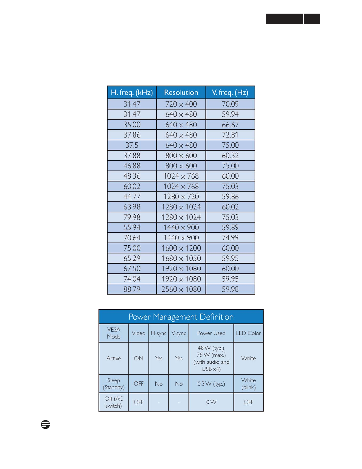
4.2 Resolution & Preset Modes
Maximum Resolution
2560 x 1080 at 60 Hz (digital input)
Recommended Resolution
2560 x 1080 at 60 Hz (digital input)
Power Management Definition
Note:
This data is subject to change without notice.
!
!
Meridian 3
12
4.3 Pixel Defect Policy
Philips strives to deliver the highest quality products.
We use some of the industry's most advanced
manufacturing processes and practice stringent quality
control. However, pixel or sub pixel defects on the TFT
Monitor panels used in flat panel monitors are
sometimes unavoidable. No manufacturer can
guarantee that all panels will be free from pixel defects,
but Philips guarantees that any monitor with an
unacceptable number of defects will be repaired or
replaced under warranty. This notice explains the
different types of pixel defects and defines acceptable
defect levels for each type. In order to qualify for repair
or replacement under warranty, the number of pixel
defects on a TFT Monitor panel must exceed these
acceptable levels. For example, no more than
0.0004% of the sub pixels on a monitor may be
defective. Furthermore, Philips sets even higher quality
standards for certain types or combinations of pixel
defects that are more noticeable than others. This
policy is valid worldwide.
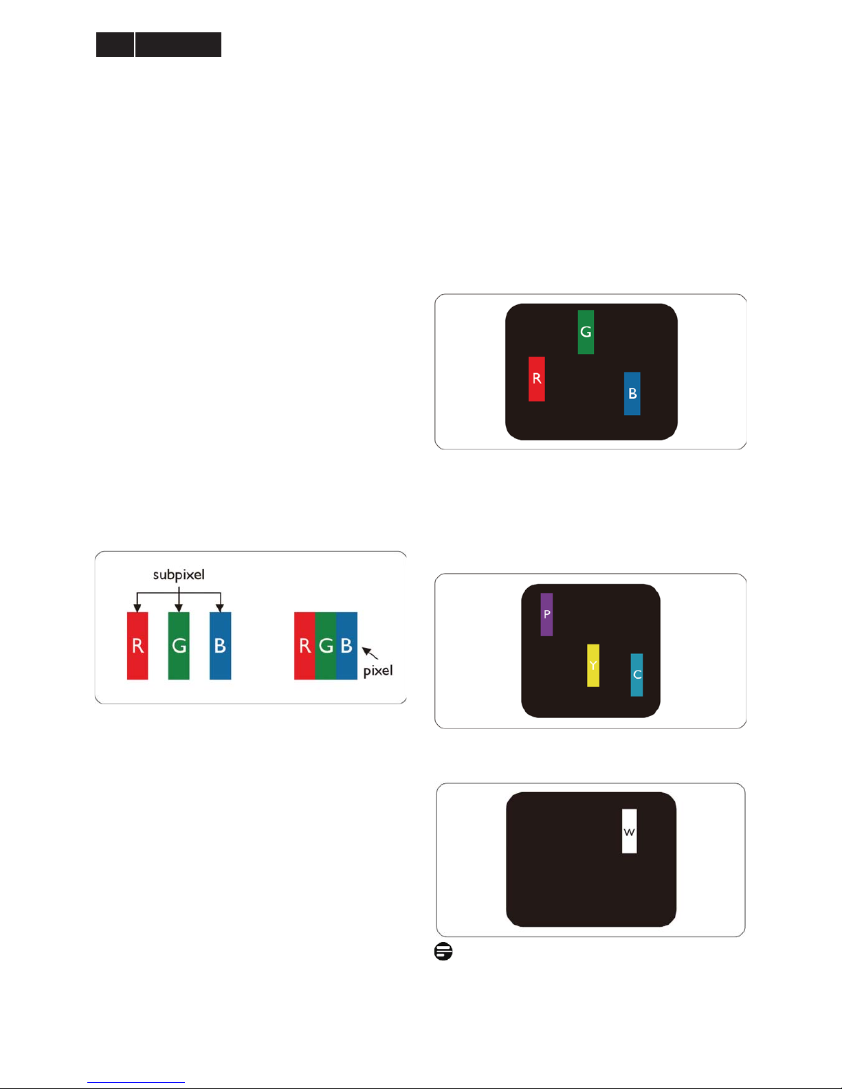
Pixels and Sub pixels
A pixel, or picture element, is composed of three sub
pixels in the primary colors of red, green and blue.
Many pixels together form an image. When all sub
pixels of a pixel are lit, the three colored sub pixels
together appear as a single white pixel. When all are
dark, the three colored sub pixels together appear as a
single black pixel. Other combinations of lit and dark
sub pixels appear as single pixels of other colors.
Types of Pixel Defects
Pixel and sub pixel defects appear on the screen in
different ways. There are two categories of pixel
defects and several types of sub pixel defects within
each category.
Bright Dot Defects
Bright dot defects appear as pixels or sub pixels that
are always lit or 'on'. That is, a bright dot is a sub-pixel
that stands out on the screen when the monitor
displays a dark pattern. There are the types of bright
dot defects.
One lit red, green or blue sub pixel.
Two adjacent lit sub pixels:
- Red + Blue = Purple
- Red + Green = Yellow
- Green + Blue = Cyan (Light Blue)
Three adjacent lit sub pixels (one white pixel)
Note:
A red or blue bright dot must be more than 50 percent
brighter than neighboring dots while a green bright dot
is 30 percent brighter than neighboring dots.

13
Meridian 3
Black Dot Defects
Black dot defects appear as pixels or sub pixels that
are always dark or 'off'. That is, a dark dot is a
sub-pixel that stands out on the screen when the
monitor displays a light pattern. These are the types of
black dot defects.
Proximity of Pixel Defects
Because pixel and sub pixels defects of the same type
that are near to one another may be more noticeable,
Philips also specifies tolerances for the proximity of
pixel defects.
Pixel Defect Tolerances
In order to qualify for repair or replacement due to pixel
defects during the warranty period, a TFT Monitor
panel in a Philips flat panel monitor must have pixel or
sub pixel defects exceeding the tolerances listed in the
following tables.
Note:
1. 1 or 2 adjacent sub pixel defects = 1 dot defect
2. This monitor is ISO9241-307 compliant, Class-I compliant.(ISO9241-307: Ergonomic requirement , analysis an d
compliance test methods for electronic visual displays)
3. ISO9241-307 is the successor of formerly known ISO13406 standard, which is withdrawn by the International
Organisation for Standardisation (ISO) per: 2008-11 -13.
!
!
Meridian 3
14
4.4 Failure Mode Of Panel
Failure description
Phenomenon
Vertical block defect
Vertical dim lines
Vertical lines defect
(Always bri
g
ht or dark)
Horizontal block defect
Horizontal dim lines
Horizontal lines defect
(Always bri
g
ht or dark)
Has bri
g
ht or dark pixel
Polarizer has bubbles
Polarizer has bubbles
Foreign material inside
polarizer. It shows liner or
dot shape.
Concentric circle formed
Bottom back light of LCD is
brighter than normal
Back light un-uniformity
Backli
g
ht has foreign material.
Black or white color, liner or
circular type
Quick reference for failure mode of LCD panel
this pa
g
e presents problems that could be made by LCD panel.
It is not necessary to repair circuit board. Simply follow the mechanical
instruction on this manual to eliminate failure by replace LCD panel.
15
Meridian 3
5. Block Diagram
5.1 Scaler Board
STD9320
Scaler IC
USBHub
Key
board
Power
sensor
webcam
DVIDPIN HDMI1 HDMI2 DPOut
Audio
DCͲDC
LDO
19V 5V
5V
2.5V
1.2V
IIC
speaker
input input input input output
3.3v
5v
Panel
lvds
12v
!
!
Meridian 3
16
5.2 Power Board
POWER BO ARD BL O CK DI AG RAM
Inrush
Prevention
Input AC Source
85v / 60 Hz ~
264v / 50 Hz
EMI Filter
Circuit
Rectification
Main
Transformer
Switching Circuit
( PWM Control IC
& MOSFET )
Rectification
Feedback
Control
Circuit
B+
Diode Rectifier
and Filter Circuit
Output (+5V) To Main board
Fuse For OLP
Diode Rectifier
and Filter Circuit
Output (+16V) to Converter Board
Diode Rectifier
and Filter Circuit
PWM Control Circuit
( PWM Control IC _O2_OZ9998AGN )
Boost C ircuit and Drive Ci rcui t
LED Light Bar
Abnormal Protect
Control Circuit
Feedback Control
Circuit
Dimming
Dimming Control Signal
(Burst model Signal )
ON / OFF Control Signal
( 5v: on / 0v:off )
Converter Block Circuit
Adapter Block Circuit
PFC BLOCK
Fuse For LPS
17
Meridian 3
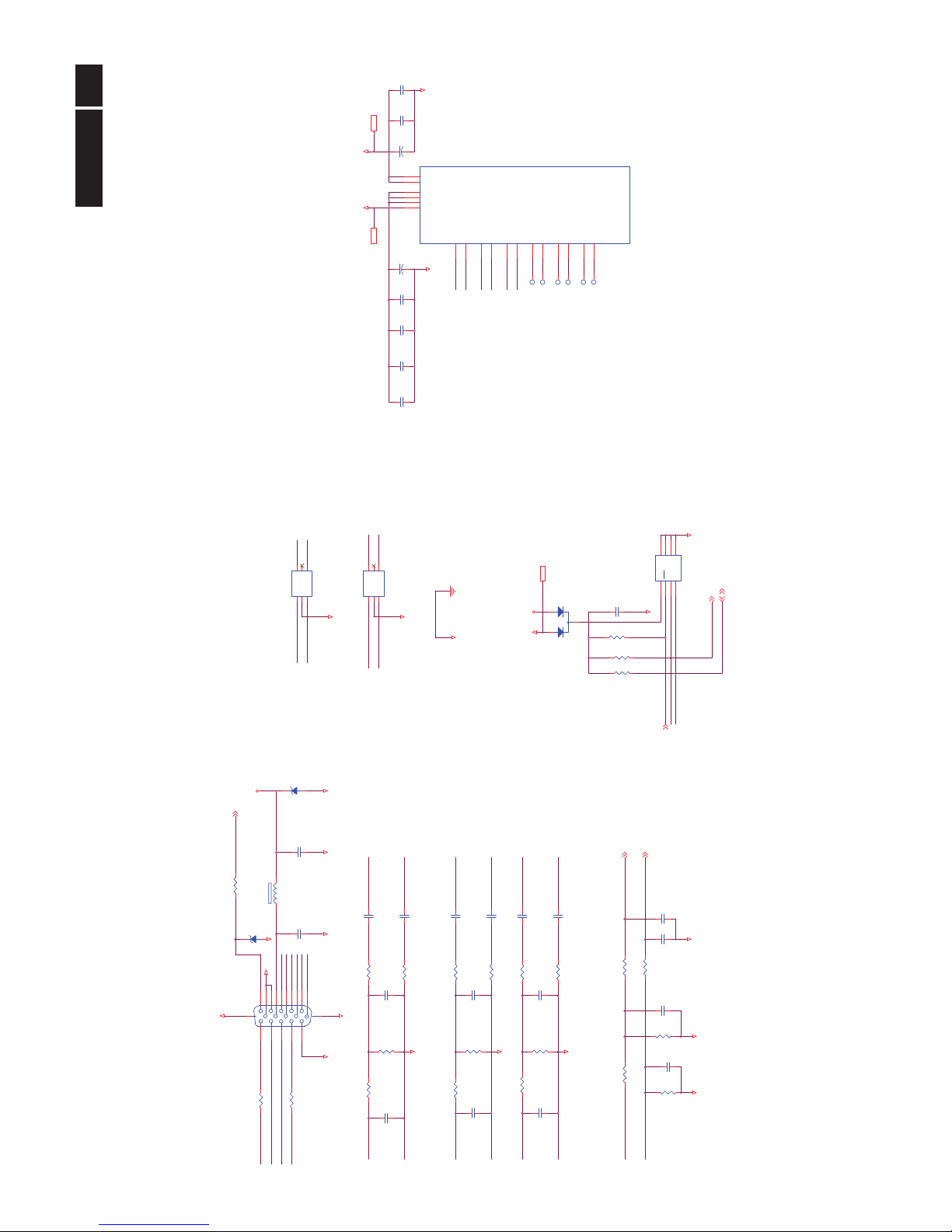
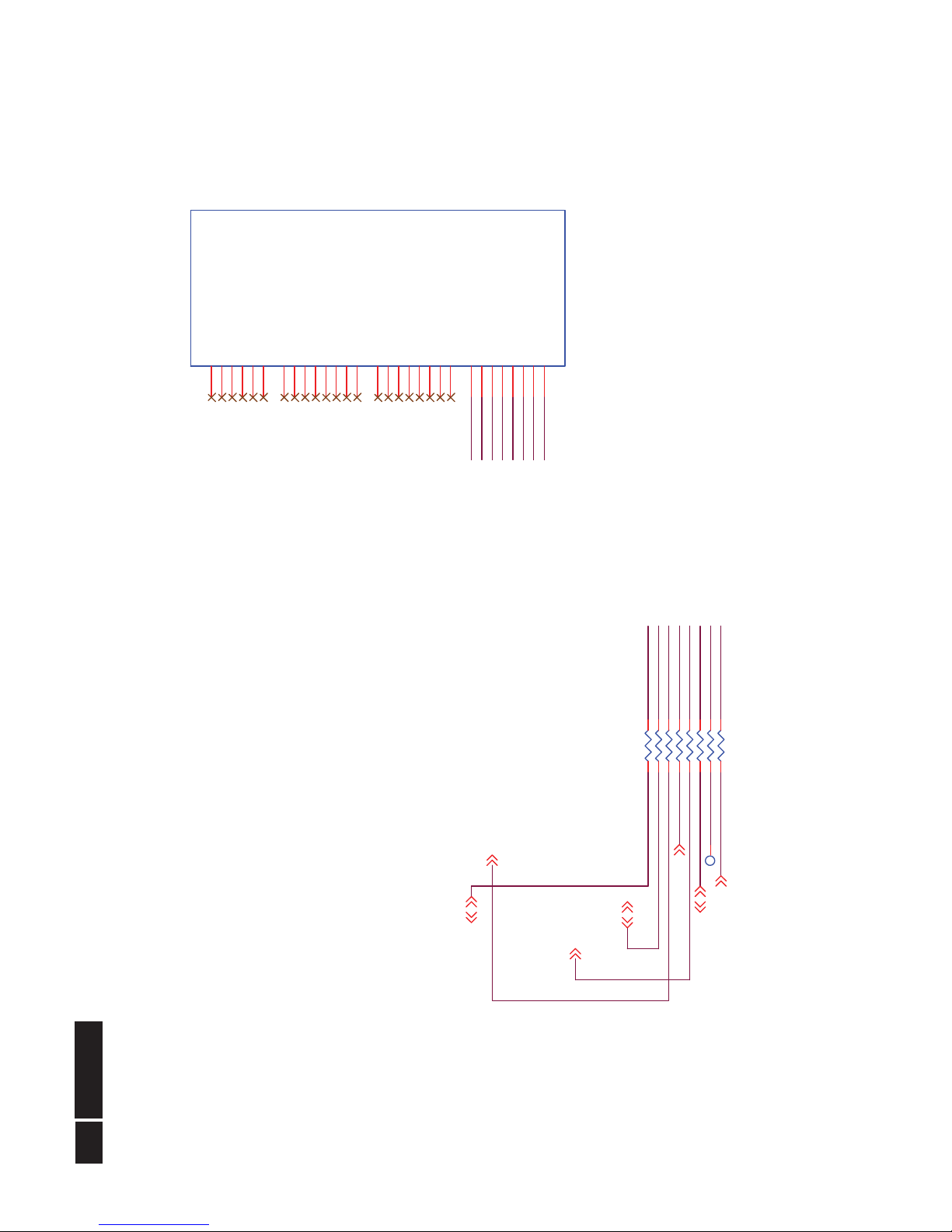
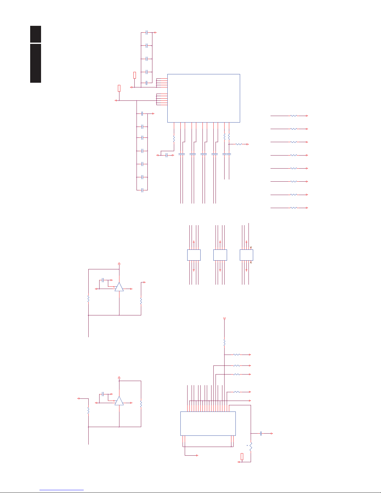
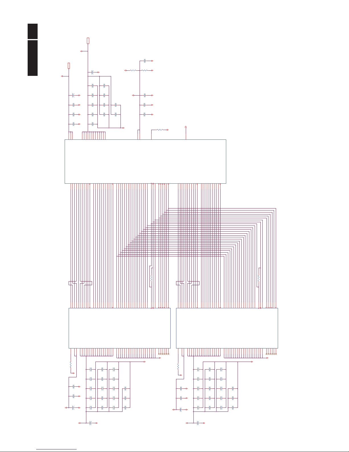
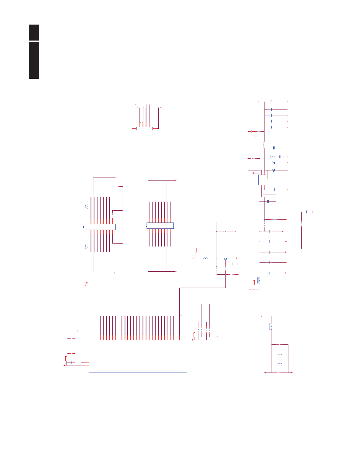
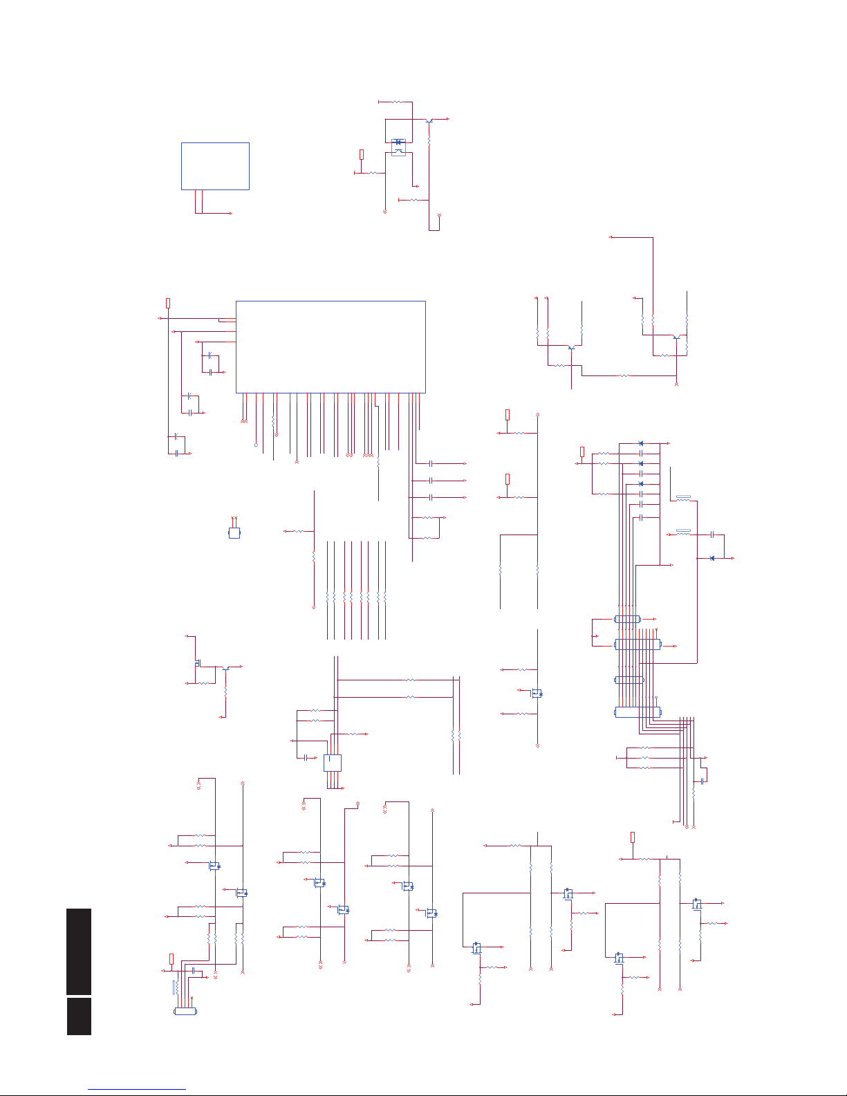
6. Schematic
6.1 Scaler Board (715G5497M01001005K)
Remark: Parts position can be searched by using FIND function in PDF.
CN101
NC/DB15
1728394105
1112131415
17 16
6
TP101
C101
100NF 25V
R108
NC/0R05 1/10W
R117
NC/22 OHM 1/16W
C112
NC/5PF 50V
ZD102
NC/R LZ5.6B
1 2
R106NC/4.7K1/16W
C119
100NF 25V
TP104
D101
NC/BAV70
3
1
2
R122 NC/100OHM
C125
1N 50V
R114
NC/75R 1/10 W 1%
Athena Analog
Front End
U401B
STDP9320
Y_P
A14
VGA_B_P
A10
VGA_G_P
A11
PB_P
A13
VGA_G_N
B11
PB_N
B13
PR_P
A15
VGA_R_P
A12
Y_N
B14
VGA_B_N
B10
VGA_R_N
B12
VDD2V5_LPM_ADC
E15
VDD1V2_LPM_ADC
E10
PR_N
B15
VDD1V2_LPM_ADC
E11
VDD2V5_LPM_ADC
E14
VDD2V5_LPM_ADC
E12
VDD2V5_LPM_ADC
E13
C117 NC/100N 16V
C110 NC/100N 16V
R115
NC/56 OHM 1/16W
C120
1N 50V
R120 NC/0R05 1/10W
C109 NC/100N 16V
R101
NC/47R 1/1 0W 5%
C126
NC/22P 50V
C114 NC/100N 16V
R107NC/4.7K1/16W
C102
NC
C129
NC/22P 50V
FB101 NC/120R 6A
1 2
C118
1N 50V
TP106
R116
NC/0R05 1/10W
TP103
R123
NC/2. 2K1/16W
R113
NC/22 OHM 1/16W
R110
NC/75R 1/10 W 1%
R103
NC/47R 1/1 0W 5%
C123
22UF 16V
C105 100N 16V
C104220N 10V
R105NC/22K1/16W
BIN0-
RIN0-
R111
NC/56 OHM 1/16W
R121 NC/100OHM
C122
22UF 16V
C128
NC
BIN0-
C115
NC/5PF 50V
C111
NC/5PF 50V
C107
NC/5PF 50V
C124
100NF 25V
C116
NC/5PF 50V
TP105
TP102
R124
NC/2. 2K1/16W
R119
NC/56 OHM 1/16W
C121
100NF 25V
R109
NC/22 OHM 1/16W
R112
NC/0R05 1/10W
R118
NC/75R 1/10 W 1%
C127
NC
C113 NC/100N 16V
C108
NC/5PF 50V
GND
+2.5V_LPM_ADC
GND
VGA_5V
+1.2V_LPM_ADC
+5V_ON
VGA_5V
GND_POWER
GND
GND
GND
GND
GND
GND
GND
GND
GND
GND
GND
GND
GND
GND GNDGND
GND
GND
modify EDID_W P1
U101
NC/ M24C 02- RMN6 TP
E01E12E2
3
VSS
4
SDA5SCL6WC7VCC
8
U102
NC/AZC398-04S
I/O11GND2I/O2
3
I/O3
4
NC
5
I/O4
6
VGA_SDA
U103
NC/AZC398-04S
I/O11GND2I/O2
3
I/O3
4
NC
5
I/O4
6
+2.5V_LPM_ADC15
+1.2V_LPM_ADC 15
R102 NC/100OHM
VGA_CABLE
GIN0-
ZD101
NC/R LZ5.6B
1 2
HSIN0
VGA_SCL
GND
GIN0
Swap R & B for layout
+5V_ON 5,10, 11,13,15
BIN0
RIN0
VGA_CABLE
VGA_SCL1
VGA_SCL
VGA_SDA
BIN0
AHS
AVS
VSIN0
HSIN0
VSIN0
VGA_SDA1
EDID_WP1
VGA_CABLE 11
AIP_AHS 11
AIP_AVS 11
VGA_SCL 3,11,16
RIN0
EDID_W P15
VGA_SDA
VGA_SCL
GIN0
RIN0
BIN0
GIN0-
GIN0
RIN0-
R0+
VSIN0
HSIN0
R0-
G0+
B0+
G0-
B0-
VGA_SDA1
VGA_SCL1
R0-
B0-
G0+
R0+
G0-
B0+
VGA_SDA 3,11
Analog Input
!
18
Meridian 3
Remark: Parts position can be searched by using FIND function in PDF.
DIN_0
TP159
DIN_2
DIN_3
DIN_6
DIN_7
DIN_1
DIN_4
LPM_DVI_SCL 11
LPM_DVI_SDA11
LPM_HDMI_SDA11
LPM_HDMI_SCL11
VGA_SDA_UDO 11
DIN_5
R158 NC / 0R 05 OH M
R159 0R05 OH M
R156 NC / 0R 05 OH M
R160 NC / 0R 05 OH M
R157 NC / 0R 05 OH M
R154 NC / 0R 05 OH M
R155 NC / 0R 05 OH M
R131 0R05 OH M
Athena DIGITAL
INPUT PORT
U401F
STDP9320
DIN_CK0
A24
DIN_CK1
B24
DIN_VS
A23
DIN_HS_CS
B23
DIN_0
B22
DIN_1
C22
DIN_2
D22
DIN_3
A21
DIN_4
B21
DIN_5
C21
DIN_6
D21
DIN_7
A20
DIN_8
B20
DIN_9
C20
DIN_10
D20
DIN_11
A19
DIN_12
B19
DIN_13
C19
DIN_14
D19
DIN_15
A18
DIN_16
B18
DIN_17
C18
DIN_18
D18
DIN_19
A17
DIN_20
B17
DIN_21
C17
DIN_22
A16
DIN_23
B16
DIN_HREF_DE
A22
DIN_ODD
C24
R 154, R156, R155, R157,
R 158, R160 chang e to NC
- 20121227
BL_EN 13
VGA_SCL_UDI11
A d d t race L PM _DVI_SDA /
LP M _DVI_SC L - 20121203
DIN_0
DIN_1
DIN_3
DIN_2
DIN_4
DIN_5
DIN_6
DIN_7
Digital Input Port
19
Meridian 3
Remark: Parts position can be searched by using FIND function in PDF.
R1170
3.3K 1/16W
GND
C166
100NF 25V
R178
1M 1/16W
C169
10UF 10V
C176 100NF 25V
C162
NC100NF 25V
t
F552
NC/PTCR
1 2
R165 1M 1/16W
C168
100NF 25V
C173
100NF 25V
R164 10K
R176
0R05 OHM
C164
100NF 25V
C163
1N 50V
C165
1N 50V
C177 100NF 25V
C167
1N 50V
D162
AOZ8804DI
CH11CH22VN3CH34CH4
5
NC6NC
7
VN
8
NC9NC
10
D163
AOZ8804DI
CH11CH22VN3CH34CH4
5
NC6NC
7
VN
8
NC9NC
10
C178
100NF 25V
R166
249R 1%
R162 1M 1/16W
C172
1N 50V
C175
100NF 25V
C170
10UF 10V
D161
AOZ8804DI
CH11CH22VN3CH34CH4
5
NC6NC
7
VN
8
NC9NC
10
R161
100K
R177
1M 1/16W
C171
100NF 25V
C174
1N 50V
R163 10K
R175 100OHM
C161
NC100NF 25V
GND
GND
GNDGND GND GND
GND
+3.3V_I/ O
+1.2 V_LP M_COMBO
+3.3V_ LPM_COMBO
GND
+3.3V_LPM_COMBO
+3.3V_LPM_COMBO
+3.3V_ LPM_COMBO
GND
GND
GND
GND
+3.3V_LPM_COMBO
GND
GND
GND
GND
GND GND
GND
GND
GND
Athena
Combo-PHY0
Input
U401C
STDP9320
CP0_3NL2CP0_3PL1CP0_2NK2CP0_2PK1CP0_1NJ2CP0_1PJ1CP0_0NH2CP0_0PH1CP0_AUXNG1CP0_AUXP
G2
CP0_REXT
G3
VDD1V2_LPM_COMBO
Y5
VDD3V3_LPM_COMBO
L5
VDD3V3_LPM_COMBO
K5
VDD3V3_LPM_COMBO
M5
VDD1V2_LPM_COMBO
W5
VDD1V2_LPM_COMBO
V5
VDD1V2_LPM_COMBO
U5
VDD1V2_LPM_COMBO
T5
VDD1V2_LPM_COMBO
AA5
VDD3V3_LPM_COMBO
N5
VDD3V3_LPM_COMBO
P5
+1.2V_LPM_COMBO 15
+3.3 V_LP M_COMBO 5,15
+3.3V_I/O 8,9,10,11,12,14
R183 22 OHM 1/16 W
R182 22 OHM 1/16 W
CN103
DP CONN
SHELL1
21
SHELL2
22
ML_ Lane 3(n)
1
GND
2
ML_ Lane 3(p)3ML_ Lane 2(n)
4
GND
5
ML_ Lane 2(p)6ML_ Lane 1(n)
7
GND
8
ML_ Lane 1(p)9ML_ Lane 0(n)
10
GND
11
ML_ Lane 0(p)
12
GND13GND
14
AUX_CH(p)
15
GND
16
AUX_CH(n)
17
Hot Plug Detect
18
Return
19
SHELL4
24
SHELL3
23
DP_PWR
20
DPRX_L2N
DPRX_AUXN
DPRX_HotPlug
DPRX_AUXP
DPRX_L3N
DPRX_AUXP
DPRX_L3N
DPRX_HotPlug
DPRX_AUXN
DPRX_L3P
DPRX_L2PDPRX_L2P
DPRX_L2N
DPRX_L3P
C179 100NF 25V
R167
100K1/16W
GND
DPRX_L0N
DPRX_L1P
DPRX_L0N
DPRX_L1P
DPRX_L0P D PRX_L0P
DPRX_L1NDPRX_L1N
DPRX_L3N
C180 100NF 25V
C181 100NF 25V
C182 100NF 25V
C183 100NF 25V
C184 100NF 25V
C185 100NF 25V
C186 100NF 25V
R168
100K1/16W
DPRX_L3P
GND
R169
100K1/16W
GND
DPRX_L2N
R170
100K1/16W
GND
DPRX_L2P
R171
100K1/16W
R173
100K1/16W
R174
100K1/16W
GND
R172
100K1/16W
GNDGND GND
DPRX_L1N
DPRX_L0N
DPRX_L1P
DPRX_L0P
DPRX_CABLE_DETECT 11 DPRX_SOURCE_POWER 11
DPRX_HPD 11
DPRX_PWR
DPRX_L3P
DPRX_L2N
DPRX_L2PDPRX_L2N
DPRX_L2P
DPRX_L1N
DPRX_L1N
DPRX_L1P
DPRX_L0N
DPRX_L0P
DPRX_L1P
DPRX_AUXN
DPRX_L0N
DPRX_L3P
DPRX_L0P
DPRX_AUXP
DPRX_AUXN
DPRX_AUXP
DPRX_AUXN
DPRX_HotPlug
DPRX_AUXP
DP Input
DPRX_L3N
DPRX_L3N
U162
NC74LVC1G125G V
2 4
513
U163
NC74LVC1G125GV
2 4
513
DisplayPort Input
!
20
Meridian 3
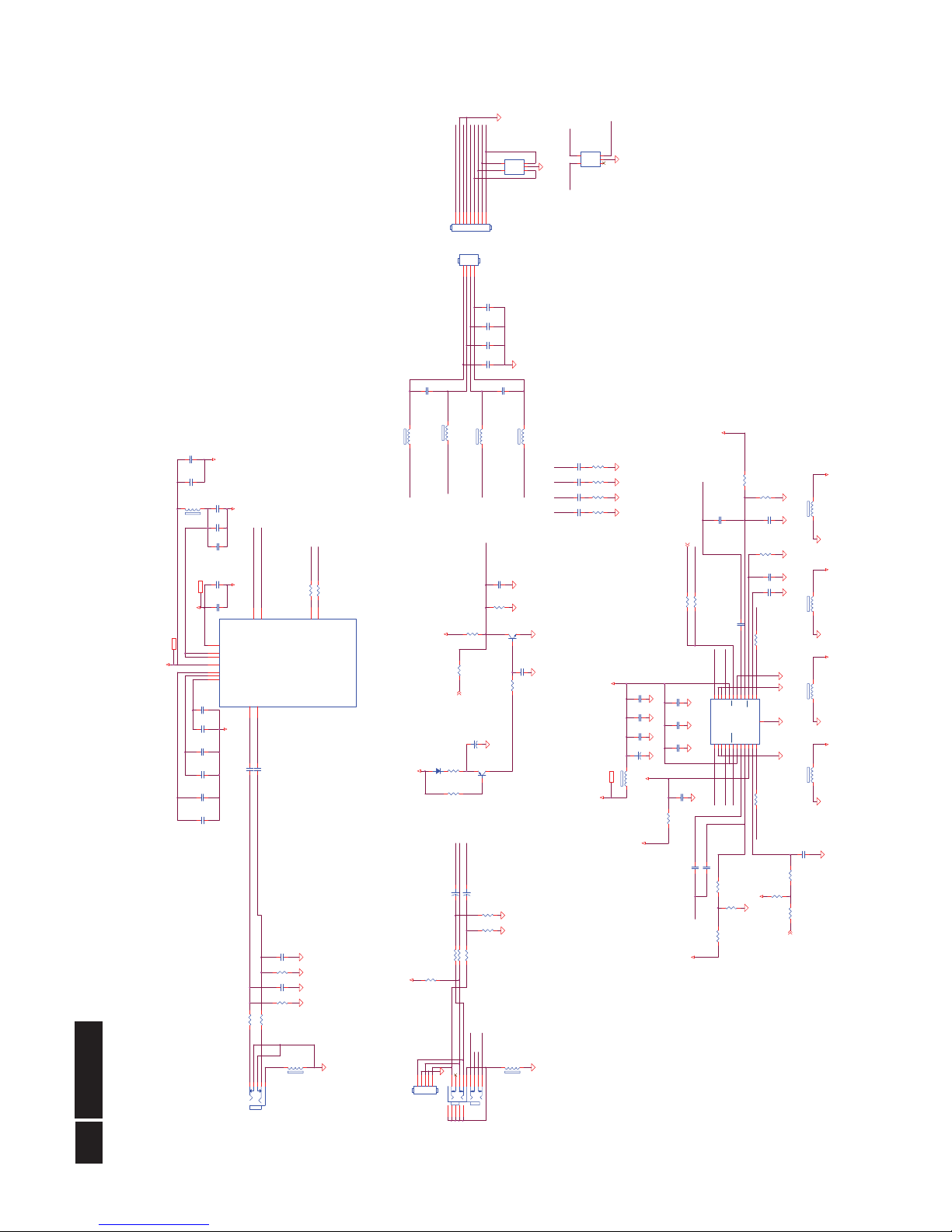
Remark: Parts position can be searched by using FIND function in PDF.
DVIR1-
DAT3+
DVIB1-
DVIG1+
DVIR1+
DAT4+
DAT3-
DVIG1-
U512
AZC398-04S
I/O11GND2I/O2
3
I/O3
4
NC
5
I/O4
6
DAT5+
DAT4-
DVIB1+
DAT5-
DVI_CLK-
DVI_CLK+ DVICLK+
DVICLK-
HDMI_SCL
TMDS_D 1+
TMDS_D 2-
TMDS_C LK-
TMDS_C LK+
H1_CK-
R1+
H1_D1+
SEL2
TMDS_D 0+
H2_D0+
H1_CK+
HDMI_OE#
R1-
TMDS_D 0-
H2_SDA
H1_D2-
H1_D1-
HDMI_SDA
H1_SCL
H2_CK+
G1-
G1+
TMDS_D 2+
TMDS_D 1-
B1+
H2_D0-
H2_D1-
B1-
H2_SCL
H1_SDA
SEL1
Delete TP502, TP501, TP504, TP505
R515, R517, R522, R524, R529, R531,
R533, R534 change to 10_ohm
Delete TP502, TP501, TP504, TP505
H1_D2+
H1_D0+
H2_D2-
H2_D1+
H2_HPD
H2_D2+
H2_CK-
H1_D0-
DAT0-
DAT0+
DAT1+
DAT1-
H1_CON_HP
DAT3+
DAT2-DAT2-
DAT3-
DAT2+
DAT3+
DAT2+
DAT3-
DAT4- DAT4-
DAT5+DAT5+
DAT4+
GNDGND
DAT5-
DAT4+
DAT5-
DVI_CLK+
H1_CON_SCL
DVI_CLK+
CLK_DDC2
DAT_DDC2
CLK_DDC2
DVI_CLK- DVI_CLK-
DAT_DDC2
C523
1N 50V
GND
H1_CON_SDA
H2_CON_CEC
H1_CON_CABLE
H1_D2+
H1_CON_HP
H1_D1+
H1_D1-
H1_D0-
H1_D0+
H1_CON_CEC
H1_CK+
H1_CK-
H1_D2-
H1_CON_SCL
Athena
Combo-PHY1
Input
U401D
STDP9320
CP1_3NT2CP1_3PT1CP1_2NR2CP1_2PR1CP1_1NP2CP1_1PP1CP1_0NN2CP1_0PN1CP1_AUXNM1CP1_AUXP
M2
CP1_REXT
M3
TMDS_D2+
TMDS_D2-
Athena
Combo-PHY2
Input
U401O
STDP9320
CP2_3N
AA2
CP2_3P
AA1
CP2_2NY2CP2_2PY1CP2_1NW2CP2_1PW1CP2_0NV2CP2_0PV1CP2_AUXNU1CP2_AUXP
U2
CP2_REXT
U3
TMDS_D1+
TMDS_D1-
TMDS_D0+
H1_HPD
H1_CON_CABLE
TMDS_D0-
TMDS_CLK+
TMDS_CLK-
H1_CON_CEC
D5V
DE5V
R556
6.2K 1/16W
Q504
LMBT3904LT1G
R555
33K 1/16W
GND GND
R567
33K 1/16W
+5V_H1
+5V_H2
Q505
LMBT3904LT1G
R568
6.2K 1/16W
H2_CON_CABLE
H2_CK-
H2_D0+
H2_CON_CABLEH2_CON_HP
H2_CK+
H2_CON_SCL
H2_SCL
H2_CON_CABLE
H2_SDA
H2_D1-
H1_CK-
H2_D2+
H2_D0-
H2_D2-
H1_D2-
H2_CON_SDA
H1_D2+
DVIG- G-
H2_CON_SCL
H2_CON_HP
H2_D1+
H2_CON_SDA
H2_CK+
DVIG+ G+
H2_HPD
H2_D1+
H1_CK+
DVICLK+ CLK+
H2_CON_CEC
H2_D2-
H2_D0-
H2_CON_SDA
B+DVIB+
DAT0-
DAT0+
H2_D1-
H2_D0+
DAT1-
DAT1+
H2_CON_HP
DVIR+ R+
H2_D0-
H2_D2+
CLK_DDC2
DVICLK- CLK-
H2_CK-
H2_D2+
H2_D1+
H2_CK-
DWP
B-
H2_D2-
B+
G-
H2_CK+
H1_SDA
R-DVIR-
H2_D0+
G+
B-DVIB-
H1_SCL
H1_D1+
H1_D1-
H1_D0-
R-
R+
H1_D0+
CLK-
CLK+
H2_D1-
H2_CON_SCL
5V_HDMI-2
H1_D0-
H1_D0+
H1_D1-
H1_D1+
H1_HPD
H1_CK+
H1_D2+
H1_D2-
H1_CK-
DHPD
DVI_DET0
U503
M24C02 -RMN6 TP
E01E12E2
3
VSS
4
SDA5SCL6WC7VCC
8
R566 4.7 OHM +-5% 1/16W
C522
1UF 16V
C513
220N 10V
R506
10K 1/10W 5%
U504
PI3HDMI1310-AZ LEX
GND1D2-A2D2+A3D3-A4D3+A5VDD6D0-B7D0+B8D1-B9D1+B10D2-B11D2+B12VDD13D3-B14D3+B15GND16D0-C17D0+C18D1-C19D1+C20VDD21D2-C22D2+C23D3-C24D3+C25GND
26
GND
27
DDC_DataA
28
DDC_CLKA
29
GND
30
DDC_DataB
31
DDC_CLKB
32
VDD50
33
DDC_DataC
34
DDC_CLKC
35
GND
36
GND37GND38GND39GND40GND
41
DDC_CLK
42
DDC_Data
43
VDD
44
D3+
45
D3-
46
GND
47
D2+
48
D2-
49
VDD
50
D1+
51
D1-
52
GND
53
D0+
54
D0-
55
VDD
56
OE#
57
SEL158SEL2
59
HPD_SINK
60
VDD
61
GND
62
GND
63
VDD50
64
HPDA
65
HPDB
66
HPDC
67
D0-A
68
D0+A
69
D1-A
70
D1+A
71
GND
72
HEATGND
73
R543 47 OHM 1/16W
R564 4.7 OHM +-5% 1/16W
R534 10 OHM
L502
90 ohm
1
4
2
3
R517 10 OHM
C503
NC
C501
100NF 25V
L506
90 ohm
1
4
2
3
L503
90 ohm
1
4
2
3
R570 4.7 OHM +-5% 1/16W
C512
100NF 25V
Q502
LMBT3904LT1G
R552 47 OHM 1/16W
R578 4.7 OHM +-5% 1/16W
R531 10 OHM
ZD502
RLZ5.6B
1 2
ZD504
RLZ5.6B
CN502
HDMI
TH1
20
TH2
21
D2+
1
D2 Shield
2
D2-
3
D1+
4
D1 Shield
5
D1-
6
D0+
7
D0 Shield
8
D0-
9
CK+
10
CK Shield
11
CK-
12
CE Remote
13
NC
14
DDC CLK
15
DDC DATA
16
GND
17
+5V
18
HP DET
19
TH3
22
TH4
23
R593
10K 1/10W 5%
FB501
120R
Add RX/TX tra ce t o CN502
HDMI connector -
20121203
R504
10K 1/10W 5%
D510
AOZ8804DI
CH11CH2
2
VN
3
CH34CH4
5
NC6NC7VN8NC9NC
10
R522 10 OHM
D506
BAT54C
ZD507
RLZ5.6B
1 2
R58722K1/16W
R511
249R 1%
R529 10 OHM
ZD503
RLZ5.6B
D511
AOZ8804DI
CH11CH2
2
VN
3
CH34CH4
5
NC6NC7VN8NC9NC
10
R590 47 OHM 1/16W
Q501
AO3401A
R551
10K
CN102
JACK
DAT2-
1
DAT2+
2
2/4shield
3
DAT4-
4
DAT4+
5
DDC SCL
6
DDC SDA
7
VSYNC
8
DAT1-
9
DAT1+
10
1/3shield
11
DAT3-
12
DAT3+
13
+5V
14
SYNC GND
15
HPD
16
DAT0-
17
DAT0+
18
0/5shield
19
DAT5-
20
DAT5+
21
clk shield
22
clk+
23
clk-
24
GND
26
GND
25
GND
27
GND
28
R554
249R 1%
C508
220N 10V
C519100NF 25 V
D509
AOZ8804DI
CH11CH2
2
VN
3
CH34CH4
5
NC6NC7VN8NC9NC
10
R54122K1/16W
D504
AOZ8804DI
CH11CH2
2
VN
3
CH34CH4
5
NC6NC7VN8NC9NC
10
L507
90 ohm
1
4
2
3
TP503
U502
M24C02 -RMN6 TP
E01E12E2
3
VSS
4
SDA5SCL6WC7VCC
8
L501
90 ohm
1
4
2
3
R550
10K
U501
M24C02- RMN6 TP
E01E12E2
3
VSS
4
SDA5SCL6WC7VCC
8
L
R588
1K
R547
0R05 OHM
D502
AOZ8804DI
CH11CH2
2
VN
3
CH34CH4
5
NC6NC7VN8NC9NC
10
R533 10 OHM
C509
100NF 25V
Select HDMI-1 or HDMI-2 into CP2
R5864.7K1/16W
R509 47R 1/10W 5%
R594
4.7K1/16W
D508
AOZ8804DI
CH11CH2
2
VN
3
CH34CH4
5
NC6NC7VN8NC9NC
10
C517100NF 25 V
D503
BAT54C
L505
90 ohm
1
4
2
3
R548
0R05 OHM
R576 4.7 OHM +-5% 1/16W
R537
NC/27K 1/16W
HPD_SINK: V iH: 2 ~ 5.3V Vi L: 0~0 .8V
C520100NF 25 V
R592
47K
R5854.7K1/16W
PORT B (HDMI-1)
ZD505
RLZ5.6B
DVIG1- G1-
DVIB1+ B1+
DVIR1- R1-
DVIR1+ R1+
DVIB1- B1-
R558 4.7 OHM +-5% 1/16W
R572 4.7 OHM +-5% 1/16W
R560 4.7 OHM +-5% 1/16W
R524 10 OHM
DVIG1+ G1+
R589 47 OHM 1/16W
R5404.7K1/16W
R515 10 OHM
R507 100R 1/10W 5%
R583
10K
R5394.7K1/16W
FB502
120R
C502
220N 25V
D507
AOZ8804DI
CH11CH2
2
VN
3
CH34CH4
5
NC6NC7VN8NC9NC
10
R545
1K
FB503
120R 6A
1 2
C510
NC
R553 47 OHM 1/16W
FB504
120R 6A
1 2
R519 100OHM
R546 22 OHM 1/16W
ST:pin17
TPV:pin11
R502
4K7 1/10W 5%
R508 47R 1/10W 5%
C505
100P 50V
C515100NF 25 V
HDMI_OE#
C521
10UF 10V
HDMI_CABLE
C506
100NF 25V
R503
4K7 1/10W 5%
R542 0R05 OHM
L
S2
C518100NF 25 V
R581 100OHM
D513
BAT54C
R510
1K
CN501
HDMI
TH1
20
TH2
21
D2+
1
D2 Shield
2
D2-
3
D1+
4
D1 Shield
5
D1-
6
D0+
7
D0 Shield
8
D0-
9
CK+
10
CK Shield
11
CK-
12
CE Remote
13
NC
14
DDC CLK
15
DDC DATA
16
GND
17
+5V
18
HP DET
19
TH3
22
TH4
23
R591 22 OHM 1/16W
Port A (NC)
D501
AOZ8804DI
CH11CH2
2
VN
3
CH34CH4
5
NC6NC7VN8NC9NC
10
C514100NF 25 V
R544 47 OHM 1/16W
C516100NF 25 V
L504
90 ohm
1
4
2
3
OE#
R549
NC
C504
100NF 25V
R505
0R05 OHM
X
+5V_ON 2,10,11,13,15
V33D_SW
GND
+3.3V_LPM_ COMBO 4,15
+3.3V_LPM 11,15
DVI_5V
GND
+3.3V_LPM
GND
GND GND
+3.3V_ LPM_C OMBO
V_DDC_H2
GND
GND
GND
GND
V_DDC_H1
GND
GND
+5V_ON
VDD5SB
GND
DVI_5V
GND
GND
GND
GND
GND
+5V_H2
ESD_DVI
VDD5SB
GND
GND
+5V_H2
GND
GND
GND
GND
+3.3V_ LPM_C OMBO
GND
GND
+3.3V_I/O
V_DDC_H2
GND
GND
ESD_DVI
R4410
NC
+5V_ON
GND
GND
GND
EDID_WP
L
+5V_H1
+5V_H1
DVI_5V
R4412
NC
GND
V33D_SW
GND
+3.3V_ LPM_CO MBO
GND
GND
GND
GND
GND
+3.3V_ LPM_C OMBO
GND
More close
V33D_SW
+5V_ON
+5V_H2
GND
GND
V_DDC_H1
GND
+5V_ON
+3.3V_LPM_COMBO
+3.3V_LPM
GND
HDMI_HPD 11
+5V_H1
GND
EDID_WP12
H2_CABLE 11
HDMI_OE# 12
EDID_WP2,12
H1_CABLE 11
SCL_DVI11
HDMI_SCL 3,11
DVI_DET 11
HDMI_SEL2 11
SDA_DVI11
HDMI_SDA 3, 11
EDID_WP12,12
HDMI_SEL1 11
TMDS_EN 11
L
5V_HDMI-1
X
P & N may swap for layout
PORT C (HDMI-2)
DAT2-
DAT4+
DAT_DDC2
DAT5+
DAT4-
DAT1+
DAT3+
DAT5-
DAT0-
DAT1-
DAT0+
DVI_CLK+
DVI_CLK-
DAT3-
DAT2+
H
Hi-Z
TX 12
RX 12
H1_CON_SCL
H1_CON_SDA
L
HDMI-2 Input (180 deg)
HDMI_CABLE
L
modify EDID_WP1
R4411 4.7K1/16W
GND
Q4404
LMBT3904LT1G
ST:pin17
TPV:pin11
S1
U511
AZC398-04S
I/O11GND2I/O2
3
I/O3
4
NC
5
I/O4
6
H
H1_CON_SDA
SEL1/SEL2: ViH: 1.5 ~ 3.3V ViL: -0.5~0.65V
L
H1_CON_HP H1_CON_CABLE
P & N may swap for layout
H
Dual
link
DAT0+
DAT0-
DVIR+
HDMI-1 Input (1 80 deg)
DVIR-
DAT1-
DAT1+
DVIG-
DVIG+
DVIB-DAT2-
DVIB+DAT2+
EDID_WP1
R4409
3.3K 1/16W
Dual_DVI/HDMI Input
21
Meridian 3
Remark: Parts position can be searched by using FIND function in PDF.
DDR_D10 DDR_D10
DDR_D23
DDR_A3
+2.5V_D DR 14
+1.5V_D DR 14
DDR_CLKN
DDR_CASN
DDR_D1
DDR_D3
DDR_D5
DDR_D7
DDR_A0
DDR_DQSN0 DDR_DQSN0
DDR_A4
C4537
1NF 50V
DDR_A5
C4538
100NF
DDR_A10
U4501
NT5CB64M1 6DP-CF
VDD
N1
NC(A15)
M7
VSS
E1
VSSQ
B1
UDQS#
B7
VDDQ
A1
DQU6
B8
VSSQ
B9
UDM
D3
UDQS
C7
VSSQ
D1
DQU7
A3
VDDQ
A8
DQU1
C3
VDDQC1VDDQ
C9
DQU0
D7
VDDQ
D2
DQU4
A7
VSSQ
D8
DQU3C2DQU2
C8
VSSQ
E2
DQU5
A2
VDD
N9
NC(CKE1)
J9
VSS
G8
VSSQ
E8
LDQS#
G3
VDDQ
E9
DQL6
G2
VSSQ
F9
LDM
E7
LDQS
F3
VSSQ
G1
DQL7
H7
VDDQ
F1
DQL1
F7
VDDQH2VDDQ
H9
DQL0
E3
VDD
B2
DQL4
H3
VSSQ
G9
DQL3F8DQL2
F2
VSS
A9
DQL5
H8
VDD
D9
VREFDQ
H1
VSSJ2VSS
B3
CK
J7
VDD
G7
CKE
K9
WE#
L3
RAS#
J3
CK#
K7
ODT
K1
BA0M2BA1
N8
CAS#
K3
CS#
L2
A10
L7
A1P7A2P3A0
N3
VDD
K2
VSS
J8
A3N2A5P2A6R8A4P8A7R2A9
R3
A11
R7
A8
T8
VSS
M1
VDD
K8
A12
N7
NC(CS1#)L1NC(A14)T7NC(ZQ1)
L9
BA2
M3
NC
T3
RESET#
T2
VREFCAM8ZQ
L8
VDDR1VDD
R9
VSSM9VSSP1VSSP9VSST1VSST9NC(ODT1)
J1
DDR_D12 DDR_D12
DDR_D11DDR_D11
DDR_A12
DDR_D17
DDR_D7
DDR_CSN
DDR_A0
GND
DDR_A11
DDR_D21
C4564
100NF
C4563
1NF 50V
DDR_D5
Athena Frame Store
DDR Interface
U401A
STDP9320
DDR_D[0]
AE26
DDR_D[4]
AF27
DDR_D[2]
AE27
DDR_D[3]
U26
DDR_D[1]
U27
DDR_D[5]
T26
DDR_D[6]
AF26
DDR_D[7]
T27
DDR_DQM[0]
AB26
DDR_DQSP[0]
AA27
DDR_DQSN[0]
AA26
DDR_D[8]
V26
DDR_D[9]
AC26
DDR_D[10]
V27
DDR_D[11]
AD27
DDR_D[12]
W27
DDR_D[13]
AD26
DDR_D[14]
W26
DDR_D[15]
AC27
DDR_DQM[1]
AB27
DDR_DQSP[1]
Y27
DDR_DQSN[1]
Y26
DDR_D[16]
N26
DDR_D[17]
E27
DDR_D[18]
N27
DDR_D[19]
E26
DDR_D[20]
P27
DDR_D[21]
D26
DDR_D[22]
P26
DDR_D[23]
D27
DDR_DQM[2]
K26
DDR_DQSP[2]
J27
DDR_DQSN[2]
J26
DDR_D[24]
F26
DDR_D[25]
L26
DDR_D[26]
F27
DDR_D[27]
M27
DDR_D[28]
G27
DDR_D[29]
M26
DDR_D[30]
G26
DDR_D[31]
L27
DDR_DQM[3]
K27
DDR_DQSP[3]
H27
DDR_DQSN[3]
H26
DDR_A[8]
M25
DDR_A[1]
U24
DDR_A[11]
N25
DDR_A[3]
T25
DDR_A[0]
K25
DDR_BA[1]
V25
DDR_A[6]
M24
DDR_A[7]
R25
DDR_A[4]
L25
DDR_A[9]
P25
DDR_CKE
Y24
DDR_A[2]
L24
DDR_A[12]
P24
DDR_BA[0]
W24
DDR_A[5]
T24
DDR_CASN
J24
DDR_RASN
H25
DDR_CSN
J25
DDR_WEN
W25
DDR_A[10]
U25
DDR_ODT
H24
VDD2V5_P LL
G23
VDDQ_DDR
J23
DDR_CLKN
R26
DDR_CLKP
R27
DDR_VREF 1
Y25
DDR_VREF 2
G25
DDR_ZQ
K24
DDR_RESETN
R24
DDR_A[13]
N24
DDR_BA[2]
V24
REG_OUT_VDDR
AA25
VDDQ_DDR
K23
VDDQ_DDR
L23
VDDQ_DDR
M23
VDDQ_DDR
N23
VDDQ_DDR
P23
VDDQ_DDR
R23
VDDQ_DDR
T23
VDDQ_DDR
U23
VDDQ_DDR
V23
VDDQ_DDR
W23
VDDQ_DDR
Y23
VDDQ_DDR
AA23
VDD2V5_P LL
AC14
VDD2V5_P LL
AC15
U4502
NT5CB64M1 6DP-CF
VDD
N1
NC(A15)
M7
VSS
E1
VSSQ
B1
UDQS#
B7
VDDQ
A1
DQU6
B8
VSSQ
B9
UDM
D3
UDQS
C7
VSSQ
D1
DQU7
A3
VDDQ
A8
DQU1
C3
VDDQC1VDDQ
C9
DQU0
D7
VDDQ
D2
DQU4
A7
VSSQ
D8
DQU3C2DQU2
C8
VSSQ
E2
DQU5
A2
VDD
N9
NC(CKE1)
J9
VSS
G8
VSSQ
E8
LDQS#
G3
VDDQ
E9
DQL6
G2
VSSQ
F9
LDM
E7
LDQS
F3
VSSQ
G1
DQL7
H7
VDDQ
F1
DQL1
F7
VDDQH2VDDQ
H9
DQL0
E3
VDD
B2
DQL4
H3
VSSQ
G9
DQL3F8DQL2
F2
VSS
A9
DQL5
H8
VDD
D9
VREFDQ
H1
VSSJ2VSS
B3
CK
J7
VDD
G7
CKE
K9
WE#
L3
RAS#
J3
CK#
K7
ODT
K1
BA0M2BA1
N8
CAS#
K3
CS#
L2
A10
L7
A1P7A2P3A0
N3
VDD
K2
VSS
J8
A3N2A5P2A6R8A4P8A7R2A9
R3
A11
R7
A8
T8
VSS
M1
VDD
K8
A12
N7
NC(CS1#)L1NC(A14)T7NC(ZQ1)
L9
BA2
M3
NC
T3
RESET#
T2
VREFCAM8ZQ
L8
VDDR1VDD
R9
VSSM9VSSP1VSSP9VSST1VSST9NC(ODT1)
J1
REG_OUT_VDDR 14
C4523
1NF 50V
C4535
100NF
C4524
100NF
C4548
1NF 50V
C4521
1NF 50V
C4547
100NF
C4520
100NF
C4530
1NF 50V
C4550
1NF 50V
C4545
100NF
C4529
100NF
C4518
100NF
C4555
1NF 50V
C4532
1NF 50V
C4506
100NF
C4539
100NF
C4531
100NF
C4507
22UF 16V
C4553
1NF 50V
C4551
100NF
C4517
1NF 50V
DDR_A1
C4533
100NF
C4526
100NF
DDR_A13
R4503
1K 1%
C4536
100NF
DDR_CLKP
DDR_A2
C4540
100NF
C4558
1NF 50V
C4522
100NF
C4556
100NF
DDR_A9
C4560
1NF 50V
R4504
1K 1%
C4546
22UF 16V
C4561
100NF
C4549
100NF
DDR_A7
DDR_BA2
C4554
100NF
C4541
10UF 16V
DDR_A6
C4542
10UF 16V
C4552
100NF
DDR_A11
C4559
100NF
DDR_A4
DDR_A0
C4508
22UF 16V
C4557
100NF
C4528
100NF
C4502
100NF
DDR_A3
C4562
100NF
DDR_A10
DDR_A13
DDR_BA0
DDR_A5
DDR_A12
DDR_BA1
C4504
1NF 50V
DDR_A2
DDR_A1
DDR_A8
C4525
1NF 50V
C4527
1NF 50V
C4544
100NF
C4543
22UF 16V
R4505
240 OHM +-1% 1/16W
1%
C4514
100NF
C4519
22UF 16V
C4516
100NF
C4501
22UF 16V
C4509
100NF
C4534
1NF 50V
C4510
1NF 50V
C4511
100NF
C4503
100NF
C4512
1NF 50V
C4515
1NF 50V
C4505
100NF
C4513
100NF
GND GND
+1.5V _DD R
GND
+0.75V_DDR_VREF
+1.5V_DDR
GND
GND
GND
+0.75V_DDR_VREF
GND
GND
GND
+2.5V_DDR
GND
GND
GND
GNDGN D GND
GNDGNDGND GND
+0.75V_DDR_VREF
GND
GND
+1.5V_D DR
+1.5V_D DR
GND
DDR_BA1
DDR_WEN
DDR_DQSN2DDR_DQSN2
DDR_D13 DDR_D13
GND
DDR_ODT
DDR_A9
DDR_D24 DDR_D24
DDR_CLKN
DDR_D14DDR_D14
R4507 220ohm 1/16W +/ -1%
R4501
220ohm 1/16W +/-1%
DDR_RESETN
GND
DDR_A13
DDR_A7
DDR_A8
DDR_D25 DDR_D25
DDR_D15DDR_D15
DDR_RESETN
DDR_D0 DDR_D0
DDR_A8
DDR_A7
DDR_D26DDR_D26
DDR_DQM1 DDR_DQM1
DDR_ODT
DDR_A6
DDR_D27 DDR_D27
DDR_DQSP1 DDR_DQSP1
DDR_D3
DDR_A10
DDR_D2DDR_D2
DDR_D28 DDR_D28
DDR_DQSN1DDR_DQSN1
DDR_WEN
DDR_CLKN
DDR_A11
DDR_A9
DDR_CASN
DDR_RESETN
DDR_D29 DDR_D29
DDR_CLKP
DDR_A12
DDR_ODT
R4502
240 OHM +-1% 1/16W
DDR_D4DDR_D4
DDR_D16DDR_D16
DDR_D30DDR_D30
DDR_CSN
R4506
240 OHM +-1% 1/16W
DDR_RASN
DDR_A2
DDR_D17
DDR_D31DDR_D31
DDR_BA0
DDR_WEN
1Gb/2Gb DDR3
DDR_D6DDR_D6
DDR_CKE
1Gb/2Gb DDR3
DDR_D18 DDR_D18
DDR_A1
DDR_D1
DDR_DQM3 DDR_DQM3
GND
DDR_DQSP2 DDR_DQSP2
DDR_DQM2DDR_DQM2
DDR_BA2
DDR_D19
DDR_DQSP3 DDR_DQSP3
DDR_CLKP
DDR_CSN
DDR_A6
DDR_DQM0DDR_DQM0
DDR_D20DDR_D20
DDR_DQSN3DDR_DQSN3
DDR_CASN
DDR_D19
DDR_A5
DDR_D21
DDR_DQSP0 DDR_DQSP0
DDR_D22DDR_D22
DDR_D23
DDR_BA2
DDR_RASN
DDR_A4
DDR_D8DDR_D8
DDR_BA1
DDR_CKE
DDR_CKE
DDR_D9 DDR_D9
DDR_BA0
DDR_A3
DDR_RASN
Frame Stroe DDR Interface
!
22
Meridian 3
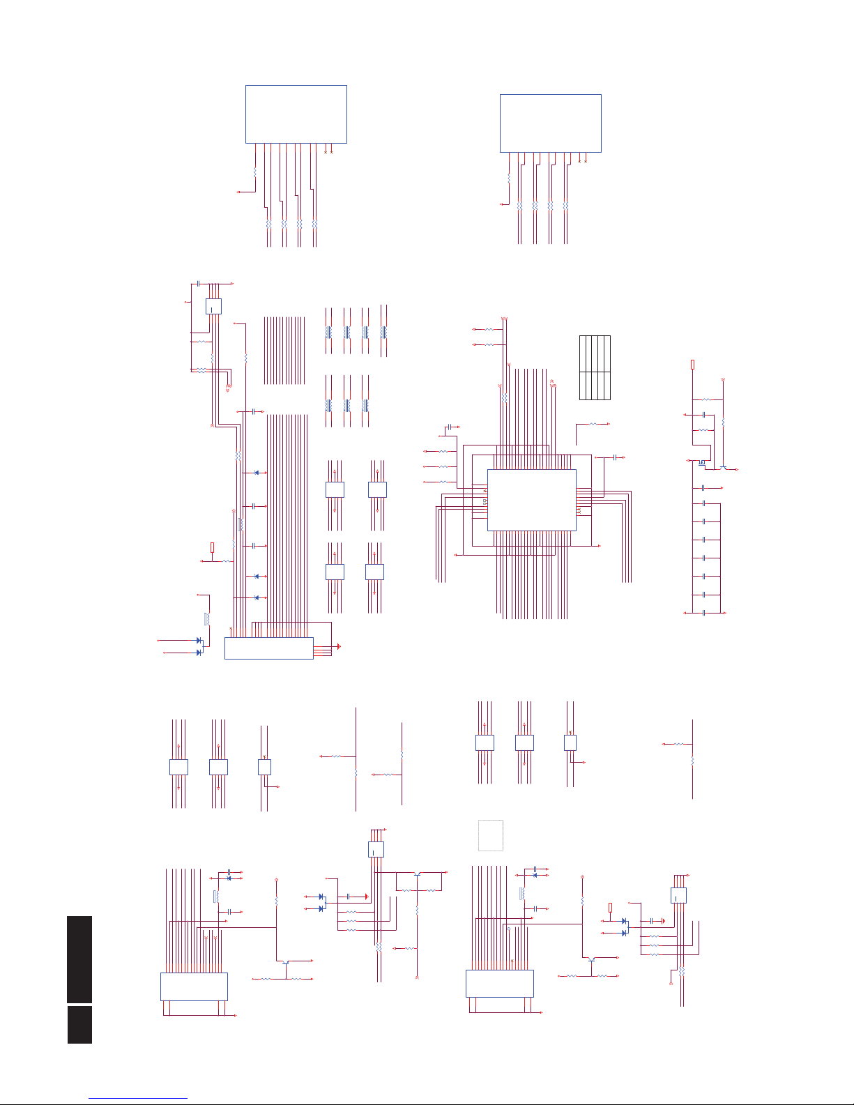
Remark: Parts position can be searched by using FIND function in PDF.
MUTE-1#
OUT-L-
Earphone_Det
Headset_R
LOUTP
OUT-R+
OUT-L+
OUT-R-
Headset_L
AUD_R1_IN
AUD_L1_IN
AGND
AGND
VOL
CN604
NC/CONN
123
4
SE
ROUTP
LOUTN
ROUTN
LINE_INPUT
DE-POP Noise
Low: shutdown Audio AMP
AUD_GAIN0
From AMP out (negative)
(active low)
From AMP out (passitive)
From AMP out (passitive)
Disable HP_OUT
To Speaker
From AMP out (negative)
UVP
EMI sol ution - 20120828
Headset_L
VOL
FB607
120R 6A
1 2
AGND
G3
Audio_5V
R610
100K 1/10W 5%
R
SE
G-2
Headset_R
G-1
Earphone_Det
L
CN605
NC/PHONE JACK
524316789
1011121314
HP_L_OUT
HP_R_OUT
HEADPHONE
CN601
NC/CONN
12345
U6681
AZ2025-04S
I/O1
1
GND
2
I/O23I/O3
4
I/O4
5
ROUTN
ROUTP
RINN
HP_L_OUT
HP_R_OUT
HP_ROUT
LOUTP
MUTE-1#
HP_LOUT
LOUTN
Athena Audio
CODEC
U401H
STDP9320
AO_LINE_LA8AO_LINE_R
B8
AO_LOUT_L
A7
AO_LOUT_R
B7
AO_HP_OUT_L
A6
AO_HP_OUT_R
B6
AUD_VBG
C7
AO_VREF_L
C8
AO_VREF_H
D7
VDDA3V3_AUD
D8
VDD3V3_HP_AUD
E7
VDD1V2_AUDIO
E8
VDD3V3_HP_AUD
E6
Headset_R
U6682
AZ2025-04S
I/O1
1
GND
2
I/O23I/O3
4
I/O4
5
Headset_L
Earphone_Det
LINN
C646
1nF
R646
10 OHM
LOUTP
OUT-L+
OUT-L-
OUT-R+G3OUT-R-
G-2
G-1
R608
NC
C631
10UF 10V
AUD_L1_OUT
C647
1nF
C628
NC
C643
1UF 16V
R647
10 OHM
R619 0R05 OHM
R618
NC
R607 NC
C636
1UF 16V
C640 1UF 16V
C632
10UF 10V
L
R
C615 0.47uF 16V
FB605 120R 6A
1 2
C616 0.47uF 16V
R625
0R05 OHM
CN603
CONN
123456789
FB613 120R 6A
1 2
C641
2.2uF 10V
R605
33K 1/10W 5%
R620 NC
C644
1UF 16V
R617
1K 1/10W 5%
R615
NC/22K
R630
100OHM
FB601 120R 6A
1 2
C625
1nF
R603 22KOHM 1/10W
C614
22UF 16V
C602
100NF 25V
FB609
120R 6A
1 2
C642
100NF 25V
C648
1nF
FB603
120R 6A
1 2
C601
NC/220p F 50V
FB606 120R 6 A
1 2
R631
10K
R649
10 OHM
C607
10UF 10V
FB611 120R 6A
1 2
R648
10 OHM
C649
1nF
C635
100NF 25V
R611
NC/10K 1/16W 5%
LOUTN
C613
1N 50V
C603
22UF 16V
C627
100NF 25V
C611
22UF 16V
ROUTP
R614 120OHM 1/10W
+
C621
NC/100uF16V
ROUTN
R624 NC/ 30K 1/16W
R627
NC/100K 1/16W 5%
C639
NC/0.47uF 16V
C619
NC/220p F 50V
FB612 120R 6A
1 2
C612
100NF 25V
D601
NC/LL4148
C605
10UF 10V
C638 NC/0.47uF 16V
R602 22KOHM 1/10W
R606 NC
FB610
0R05OHM1/8W
C637 1U F 16 V
R623
1K 1/16W 1%
C608
100NF 25V
C626
1nF
C617
470PF
C624
1nF
R621
3Kohm 1/16W +/-1%
C623
1nF
C630
10UF 10V
R613 100K 1/10W 5%
R604
33K 1/10W 5%
C609
10UF 10V
Q601
NC/MMBT3904
U601
APA2606NAI-TRG
LOUTP1PGND2PGND3LOUTN4PVDD5MUTE6VDD7LINN8UVP9VDC10VOLUME11HP_LOUT
12
HP_ROUT
13
BYPASS
14
SE/BTL
15
AGC
16
RINN
17
GND
18
SD
19
PVDD
20
ROUTN
21
PGND22PGND
23
ROUTP
24
Thernal Pad
25
CN602
PHONE JACK
12354
C606
100NF 25V
R626
0R05 OHM
C633
100NF 25V
C618
470PF
C634
100NF 25V
FB602
120R 6A
Q602
NC/MMBT3906
R601
470OHM1/16W
R616
1K 1/10W 5%
R622
30K 1/16W
C604
100NF 25V
C610
100NF 25V
FB604 120R 6 A
1 2
R629
NC/10K
R609
NC
R612 120OHM 1/10W
R628
0R05 OHM
FB608 120R 6 A
1 2
MUTE-1 #
+5V
+3.3V_AUD 14
+5V 11,12,13,14
+1.2V_AUD 14
C620, C622 from 220u F/25V
change to 220uF/16V - 20121025
Audio_5V
AGND
AGND
AGND
AGND
GND
AGNDAGND
GND
AGND
GND
AGND
AGND
AGND
AGNDAGND
AGND
VDC
GND
AGND
AGND
AGND
AGND
AGND
AGND
Audio_5V
AGND
AGND
Audio_5V
+3.3V_AUD
AGND
AGND
Audio_5V
AGND
GND
AGND
AGND
+1.2V_AUD
AGND
AGND
AGND
AGND
AGND
AGND
AGND
AGND
GND
AGND
Audio_5V
AGND
Audio_5V
GND
MAIN_MU TE12
AUD_STBY 8
Audio_5V
GND
VOLUME12
C629 from 220uF/25V
change to 220uF/16V -
20121025
+
C629
220UF 16V
+
C620 220UF 16V+C622 220UF 16V
AUD_L1_OUT
AUD_R1_OUT
AUD_R1_OUT
Add U 6681 & U6682
AZ2025-04S - 20121203
HP_L_OUT HP_R_OUT
Analog Audio
23
Meridian 3
Remark: Parts position can be searched by using FIND function in PDF.
I2S_DOUT3
To Bootstr aps sett ing
I2S_MCLK_OUT_IN
AUD_STBY
I2S_DOUT0
AUD_STBY
Athena I2S
U401L
STDP9320
I2S_DIN
AB1
I2S_WS_IN
AB2
I2S_CLK_IN
AB3
I2S_DOUT2
AC2
I2S_DOUT1
AC1
I2S_WS_OUT
AC3
I2S_CLK_OUT
AC4
I2S_MCLK_OUT_IN
AD1
SPDIF_IN
AB4
SPDIF_OUT
AD2
DCLK_GPIO86_PWM5
D23
DVS_GPIO87_I2S_DOUT0_PWM6
AF1
DHS_GPIO88_PWM7
C23
DEN_GPIO89_I2S_DOUT3_PWM8
AF2
TP606R633 0R05 OH M
TP607
R635 0R 05 OH M
TP605
TP602
R632
4.7K1/16W
TP608
TP604
TP601
TP603
R634 0R05 OH M
SPDIF_OUT 12
+3.3V_I/O
+3.3V_I/O 4,9,10,11,12,14
I2S_DOUT1 12
I2S_WS_OUT 12
I2S_DOUT2 12
AUD_STBY 7
I2S_CLK_OUT 12
I2S_DOUT1
I2S_DOUT2
AUD_DAC_RESET
I2S_CLK_OUT
SPDIF_OUT
I2S_WS_OUT
Digital Audio
!
24
Meridian 3
Remark: Parts position can be searched by using FIND function in PDF.
C541 100NF 25VR4291 0R05 OHM
C542 100NF 25V
C543 100NF 25V
C544 100NF 25V
C545 100NF 25V
C548 100NF 25V
C546 100NF 25V
C547 100NF 25V
C549 100NF 25V
C550 100NF 25V
t
F551
NC/PTCR
1 2
ZD551
RLZ5.6B
1 2
R4292 0R05 OHM
R4294 0R05 OHM
R4293 0R05 OHM
R4296 0R05 OHM
R4298 0R05 OHM
GND
R4297 0R05 OHM
R4295 0R05 OHM
R4289 0R05 OHM
R4299 0R05 OHM
C551
NC/100N16V
DPTX_L0N
DPTX_L0P
GND
DPTX_L3P
DPTX_L3P
R597
1M
DPTX_L3N
DPTX_L3N
+3.3V_I/O
DPTX_AUXN
+3.3V_I/O
DPTX_HotPlug
GND
GND
+1.2V_D PTX
R4290 249R 1%
D552
AOZ8804DI
CH11CH22VN3CH34CH4
5
NC6NC
7
VN
8
NC9NC
10
GND
D551
AOZ8804DI
CH11CH22VN3CH34CH4
5
NC6NC
7
VN
8
NC9NC
10
GND
D553
AOZ8804DI
CH11CH22VN3CH34CH4
5
NC6NC
7
VN
8
NC9NC
10
TCLK
GND
GND
GND
GND
GND GND
DPTX_AUXP
GND
DPTX_AUXN
GND
DPTX_L1P
DPTX_L1P
DPTX_L2P
DPTX_L1N
DPTX_L2P
DPTX_L2N
DPTX_L1N
DPTX_L2N
DPTX_AUXP
DPTX_L0P
DPTX_L0N
C540
100NF 25V
CN503
DP CONN
SHELL1
21
SHELL2
22
ML_ Lane 3(n)1GND2ML_ Lane 3(p)3ML_ Lane 2(n)4GND5ML_ Lane 2(p)6ML_ Lane 1(n)7GND8ML_ Lane 1(p)9ML_ Lane 0(n)10GND11ML_ Lane 0(p)12GND13GND14AUX_CH(p)15GND16AUX_CH(n)17Hot Plug Detect18Return
19
SHELL4
24
SHELL3
23
DP_PWR
20
GND
C408 & C 409 fro m 12p
chang e to 33p - 20121025
DPTX_L1P
DPTX_AUXN
DPTX_L1N
DPTX_AUXP
DPTX_L2N
DPTX_L3N
DPTX_L0P
DPTX_L3P
DPTX_L2P
DPTX_L0N
DPTX_L0P
DPTX_L0N
DPTX_L1N
DPTX_L1P
DPTX_L2P
DPTX_L2N
DPTX_L3P
DPTX_L3N
DPTX_AUXP
DPTX_AUXN
DPTX_HotPlug DPTX_HotPlug
XTAL
R598
1M
ZD552
RLZ5.6B
1 2
GND
R596
100K
C403
100NF 25V
DPTX_HotPlug
C404
1N 50V
C406
22UF 16V
C402
22UF 16V
X401
27.000MHz
12
C405
100NF 25V
C407
100NF 25 V
+1.2V_DPTX
+1.2V_DPTX
+2.5V_DPTX 14 +1.2V_D PTX 14
+1.2V_D PTX
+2.5V_D PTX
GND
GND
R595
100K
+2.5V_DPTX
+1.2V_D PTX
R512
100K
R599 100R 1/16W 5%
+3.3V_I/O
+3.3V_I/O 4,8,10,11,12,14
Athena Clock
Generation
U401K
STDP9320
DPTX_XTAL
AD14
DPTX_TCLK
AE14
DPTX_HPD 11
GND
Athena
DisplayPort
Output
U401N
STDP9320
DP_TX3N
AF11
DP_TX3P
AG11
DP_TX2N
AF12
DP_TX2P
AG12
DP_TX1N
AF13
DP_TX1P
AG13
DP_TX0N
AF14
DP_TX0P
AG14
DP_AUXTXN
AF10
DP_AUXTXP
AG10
DP_TX_REXT
AE10
VDD1V2_DPT X
AC9
VDD1V2_DPT X
AC10
VDD1V2_DPT X
AC11
VDD2V5_DPT X
AC13
Delete R402, R403 & R404 ; C408 &
C409 change to 12p F - 20120831
C409
12P 50V
C408
12P 50V
C408 & C 409 fro m 12p
chang e to 33p - 20121025
DPTX Connector
DisplayPort Output
25
Meridian 3
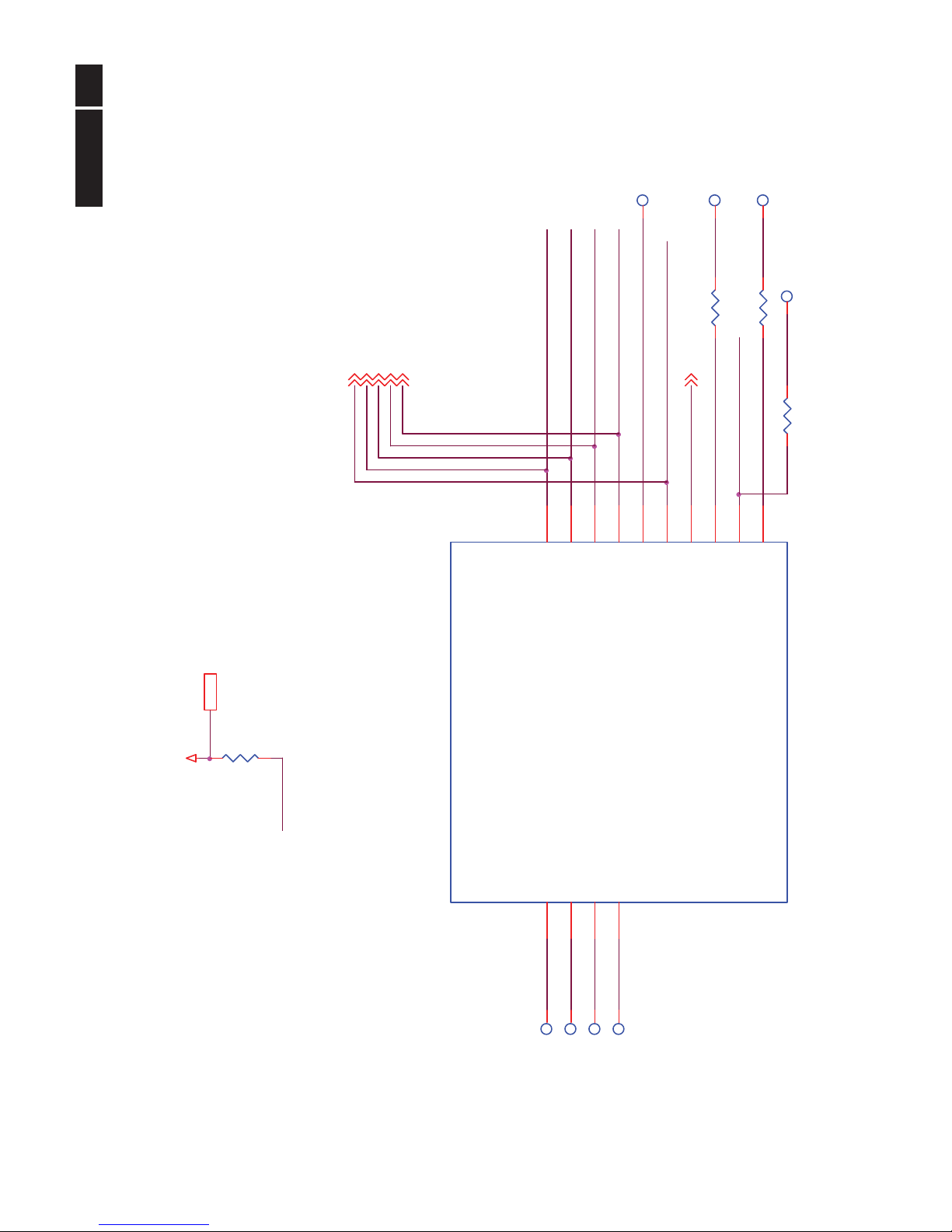
Remark: Parts position can be searched by using FIND function in PDF.
12V Panel power
L4262 change to 073G253S 87 H
(L70X70-SMD- 1) - 20120830
+19V_ON
+19V_ON 13,16
LVTX_D_CH2N
LVTX_D_CH2P
LVTX_B_CH3N
LVTX_A_CH4P
LVTX_B_CLKP
LVTX_A_CLKN
LVTX_D_CH3P
LVTX_C_CH0P
LVTX_C_CH2P
LVTX_A_CH3P
LVTX_A_CH3P
LVTX_C_CLKP
PANEL_CTRL1
LVTX_B_CH4N
LVTX_D_CH1P
LVTX_D_CH3P
LVTX_C_CH0N
PSET3
LVTX_D_CH3N
LVTX_C_CLKN
PANEL_CTRL1
DC_Panel_EN
LVTX_D_CH1N
DCP_FB
LVTX_A_CH3N
LVTX_C_CH3N
LVTX_B_CH0N
LVTX_B_CH2N
+PANEL_PWR
LVTX_C_CH4P
LVTX_C_CH0P
LVTX_B_CH2P
PBIAS
LVTX_A_CLKP
LVTX_C_CH1P
LVTX_A_CH1P
LVTX_C_CH0N
LVTX_A_CH1N
LVTX_D_CH4P
LVTX_B_CH0P
LVTX_A_CH2P
LVTX_A_CH2P
LVTX_A_CH4N
LVTX_B_CH3P
LVTX_A_CLKN
LVTX_C_CH3N LVTX_C_CH1P
LVTX_A_CH4N
LVTX_A_CLKP
LVTX_A_CH0P
LVTX_C_CH4N
P_ON5
LVTX_C_CH2N
Panel_P
LVTX_B_CH1P
LVTX_D_CH0N
LVTX_C_CLKP
LVTX_D_CLKP
PANEL_CTRL2
+PANEL_PWR
LVTX_D_CH0P
L4262 footpri nt change to L 83X 83-S M D
298P4/298X4 use 10uH same as 272P4
DCP_COMP
LVTX_B_CH4P
LVTX_B_CLKP
LVTX_A_CH3N
LVTX_B_CH2P
LVTX_C_CH1N
LVTX_B_CH1N
LVTX_D_CLKP
LVTX_C_CH4P
LVTX_B_CH0P
LVTX_D_CH2N
LVTX_D_CH1N
LVTX_C_CH1N
LVTX_B_CH3P
LVTX_D_CH1P
LVTX_D_CLKN
LVTX_D_CH2P
LVTX_A_CH2N
DCP_GND
LVTX_A_CH0P
DCP_COM
LVTX_B_CH0N
LVTX_B_CLKN
LVTX_B_CH2N
LVTX_A_CH1P
LVTX_C_CH2N
LVTX_C_CH2P
LVTX_C_CLKN
LVTX_C_CH3P
LVTX_A_CH0N
LVTX_A_CH1N
LVTX_D_CH0N
LVTX_C_CH3P
LVTX_B_CH3N
LVTX_A_CH0N
LVTX_B_CH1N
LVTX_C_CH4N
+19V_IN_Panel
PSET2
PPWR
LVTX_A_CH4P
LVTX_B_CH4P
LVTX_D_CH3N
PSET1
LVTX_A_CH2N
LVTX_B_CH4N
PANEL_CTRL2
LVTX_D_CLKN
LVTX_D_CH4P
LVTX_B_CH1P
LVTX_B_CLKN
LVTX_D_CH4N
GND
PPWR
PSET0
LVTX_D_CH0P
LVTX_D_CH4N
P_ON5
DCP_VCC
GND
FB4262
120R 6A
1 2
+2.5V_LV DS 14
+3.3V_I/O 4,8,9,11,12,14
+5V_ON 2,5,11,13,15
+5V_ON
BL_ON 13
GND
MSTR1_ SCL12
MSTR1_ SDA12
Panel_VCC = 5V
L4262 = 10uH
R4277 = 63.4K
R4262 = 12K
C4269 = 56pF
R4280 = 51K
C4284 = 1000pF
C4282
100NF 25V
GND GND
R4282
1.2K 1/4W
R4283
1.2K 1/4W
GND GND
Panel_VCC = 12V:
L4262 = 15uH
R4277 = 140K
R4262 = 10K
C4269 = 22pF
R4280 = 62K
C4284 = 820pF
GND
GND
GNDGND GND GND GND GND GN D GND GND
LVDS Connector for Third Channel & Fourth Channel
GND
+
C4272
220uF 25V
LVDS Connector for First Channel & Second Channel(Left Side)
U4262
APW7089KAI-TRG
VIN1EN2UGND3VCC
4
LX
5
COMP
6
FB
7
GND
8
LX
9
C4277
10UF 25V
R4263100OHM
R4281
30K 1/16W
R427010K
CN408
CONN
246
8
101214161820222426283032343638
40
135791113151719212325272931333537
39
D4262
SX36
1 2
+
C4283
220uF 25V
R4265100OHM
R4269 10K
D4263
SX36
1 2
R4267 0R05 1/10W
R4284
4.7K1/16W
R4271 NC/10K
C4275
100NF 25V
FB4263
48R 6A
1 2
R4268 NC/10K
CN409
CONN
246
8
10121416182022242628303234
13579111315171921232527293133
Panel_VCC
L4262
10uH
R4264 NC/ 100R 1/16W 5%
+
C4271
220uF 25V
R4278
0R05 OHM
C4273
10UF 25V
C4269
22P 50V
R4276
NC/4.7K1/16W
Athena LVTX
U401E
STDP9320
LVTX_A_CH0N
AB24
LVTX_A_CH0P
AB25
LVTX_A_CH1P
AC25
LVTX_A_CH1N
AC24
LVTX_A_CH2P
AG25
LVTX_A_CH2N
AF25
LVTX_A_CH3P
AG24
LVTX_A_CH3N
AF24
LVTX_A_CH4P
AE24
LVTX_A_CH4N
AD24
LVTX_A_CLKP
AE25
LVTX_A_CLKN
AD25
VDD2V5_LVDS
AC17
PPWR
AF4
PBIAS
AG5
LVTX_B_CH0N
AF23
LVTX_B_CH0P
AG23
LVTX_B_CH1N
AD23
LVTX_B_CH1P
AE23
LVTX_B_CH2N
AF22
LVTX_B_CH2P
AG22
LVTX_B_CLKN
AD22
LVTX_B_CLKP
AE22
LVTX_B_CH3N
AF21
LVTX_B_CH3P
AG21
LVTX_B_CH4N
AD21
LVTX_B_CH4P
AE21
LVTX_C_CH0N
AF20
LVTX_C_CH0P
AG20
LVTX_C_CH1N
AD20
LVTX_C_CH1P
AE20
LVTX_C_CH2N
AF19
LVTX_C_CH2P
AG19
LVTX_C_CLKN
AD19
LVTX_C_CLKP
AE19
LVTX_C_CH3N
AF18
LVTX_C_CH3P
AG18
LVTX_C_CH4N
AD18
LVTX_C_CH4P
AE18
LVTX_D_CH0N
AF17
LVTX_D_CH0P
AG17
LVTX_D_CH1N
AD17
LVTX_D_CH1P
AE17
LVTX_D_CH2N
AF16
LVTX_D_CH2P
AG16
LVTX_D_CLKN
AD16
LVTX_D_CLKP
AE16
LVTX_D_CH3N
AF15
LVTX_D_CH3P
AG15
LVTX_D_CH4N
AD15
LVTX_D_CH4P
AE15
VDD2V5_LVDS
AC18
VDD2V5_LVDS
AC19
VDD2V5_LVDS
AC20
C4263
22UF 16V
R4275
NC/22K1/16W
C4264
100NF 25V
C4267
1N 50V
C4279
10UF 25V
R4272 10K 1/10W 5%
C4265
1N 50V
C4270
1UF 25V
R4266 NC/ 100R 1/16W 5%
C4266
100NF 25V
R4273
100OHM
C4268
NC/100NF 25V
Q4262
NC/LMBT3904LT1G
+
C4276
220uF 25V
R4280
62K 1/16W 1%
GND
GND
+3.3V_I/O
C4262
10UF 25V
GND
+2.5V_LV DS
C4278
10UF 25V
GND
C4280
1UF 25V
GND
GND
GND
C4284
820pF 50V
+PANEL_PWR
GND
R4279
100K1/16W
R4277
140K 1%
C4285
100NF 25V
R4262
10K 1/10W 1%
C4281
22P 50V
C4274
10UF 25V
CN410
NC/CONN
123456789
10
1112
Panel_VCC
R4274
22K1/16W
GND
OUTPUT_DOUBLE LVDS
!
26
Meridian 3
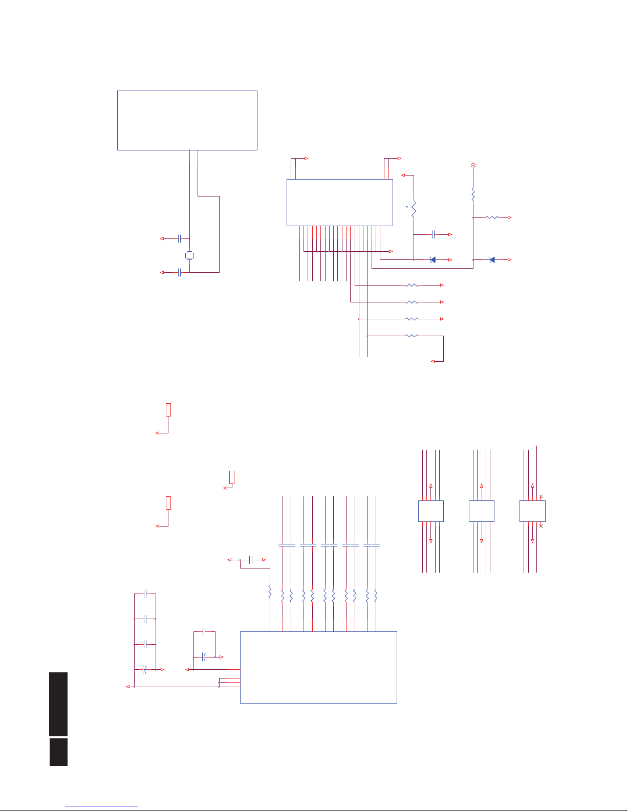
Remark: Parts position can be searched by using FIND function in PDF.
LPM_DVI_HPD
LPM_GPIO3_EDID4PS_ON
GPADC_AIN0
KEY2GPADC_AIN1
CN403
NC/CONN
1234567891011
12
(Tact SW)
R4402
10K
+2.5V_LPM
+2.5V_LPM 5,12,15
Q406
BSN20
3
1
2
TP412
LPM_DVI_SDA3
LPM_DVI_SCL 3
GND
Q401
BSN20
3
1
2
GND
GPADC_AIN0
R7438 NC/ 0R 05 1/ 10W
R740
10K
GND
GND
GND
R4457
10K 1/16W 5%
+3.3V_I/O 4, 5,8,9,10 ,12,14
R458 33K 1/10W 5%
HDMI1_HDMI2 Cable
detection
LPM_DVI_SCL
LPM_DVI_SDA
SCL_DVI
SDA_DVI
Q416
2N7002
5V/3V Level Translator
USB_ON 16
R7439 0R05 1/10W
PS_OUTPUT
USB_ON
R186
10K 1/10W 5%
R187
100K 1/10W 5%
GND
GND
R188 27K 1/10W 5%
R189 39KOHM 1/10W +/-5%
+5V_H2
HDMI_HPD
HDMI_HPD5
R44110K
+5V_H1
LPM_HDMI_HPD
Q417
2N7002
R44010K
GND
GND
R191
100K 1/10W 5%
R190
10K 1/10W 5%
PS_ON
PS_OUTPUT
+5V_ON
PS_DISTANCE
VGA_SDA_UDO
C429
100P 50V
FB403
120R
VGA_5V
GND
Q418
2N7002
R192
10K 1/10W 5%
GND
R193
100K 1/10W 5%
+3.3V_I/O
PIVOT_EN
+3.3V_I/O
OC_SW
R4455
100R 1/10W 5%
Q4466
LMBT3904LT1G
R196
10K 1/10W 5%
R197
100K 1/10W 5%
R4461
10K 1/16W 5%
OC4401
RBS311115
4 3
1 2
DVI_5V
Q419
2N7002
R4456
4.7K1/16W
GND
GND
R195 39KOHM 1/10W +/-5%
R194 27K 1/10W 5%
GPADC_AIN2
for TACT Kkey
for touch key
USB Control for 298P4
2012/10/15
USB Control for 272P4
Debug
POWER_KEY#
LPM_DVI_SCL
LED_R
TOUCH_POWER
CN411
NC/CONN
1234567891011
12
1314
+2.5V_SW
R4401
NC/10K
LPM_HDMI_SDA
LPM_HDMI_SCL
LED_GREEN
+2.5V_SW 5,12,15
R412 NC
DPTX_HPD
Q404
LMBT3904LT1G
C412
100NF 25V
R43110K
DPTX_HPD9
C418
100NF 25V
R426 0R05 OHM
R43310K
R40710K
C414
100NF 25V
LED_R
C422 NC
R41810K
LPM_SLV2_SDA
LPM_SLV2_SCL
LED_G
Q403
2N7002
R435 0R05 OHM
LPM_DVI_SDA
LPM_H DMI_ SDA3
R451
NC/1R 1/10W 5%
R448
NC/4.7K1/16W
+3.3V for touch IC power on KB)
+5V for LED power on Touch KB
LED_AMBER
U405
M24C02-RMN6TP
E01E12E23VSS
4
SDA
5
SCL
6
WC
7
VCC
8
R454
3.9K1/16W
Q402
AO3401A
R421 0R05 OHM
Q407
2N7002
Q412
LMBT3906LT1G
LPM_H DMI_ SCL 3
R437
1M 1/16W
R43410K
R455
3.9K1/16W
R461NC
R465
NC
C411
22UF 16V
R410 0R05 1/10W
VGA_SCL_UDI 3
R462NC
+3.3V_I/O
R41710K
C425
100N 16V
R419
4.7K1/16W
R409
47K
R429 0R05 OHM
R413 0R05 1/10W
R40610K
D402 RLZ5.6B
1 2
FB402
NC/120 OHM
1 2
R40510K
D404 NC/RLZ5.6B
C424
NC
R423 0R05 OHM
R427
0R05 OHM
C421 NC
CN404
CONN
1234567
D403 RLZ5.6B
1 2
C423 NC
R425 0R05 OHM
R464
2.2K1/16W
R438 100R 1/10W 5%
LPM_SLV1_SCL
Q409
2N7002
R411 4.7K1/16W
R41610K
R40810K
C410
100NF 25V
R442 NC/0R05 1/10W
LPM NVRAM
I2C addr e ss: A0H and A1H
C401
100NF 25V
LPM_SLV1_SDA
Q408
2N7002
LPM_MSTR _SC L
R467
0R05 OHM
R439 100R 1/10W 5%
Q405
2N7002
C415
22UF 16V
R414
10K 1/10W 5%
D401 RLZ5.6B
1 2
R444 NC/0R05 1/10W
LPM_SLV4_SCL
R466
560OHM +-5% 1/10W
C417
100NF 25V
FB401
NC/120 OHM
1 2
R456
22KOHM 1/10W
R43010K
R457 15KOHM 1/10W
R450
0R05 OHM
R436
1M 1/16W
R428 0R05 OHM
R422
4.7K1/16W
R460NC
R453
3.9K1/16W
R424 0R05 OHM
C413
22UF 16V
R463 0R05 1/10W
C420 NC/0.1UF 16V
R420
4.7K1/16W
R459 NC
R432 0R05 OHM
C419 NC/0.1UF 16V
DPRX_CABLE_DETECT
Q411
NC/LMBT3906LT1G
R401 NC
DPRX_SOURCE_POWER
C416
220N 10V
+3.3V_LPM 5,15
+1.2V_L PM 15
LPM_GPIO5_EDPD3
+3.3V_LPM
+5V_ON
+2.5V_LPM 15
+5V_ON 2,5,10,13,15
R181
NC/100R 1/10W 5%
+2.5V_LPM
+5V_ON
GND
+3.3V_LPM
VGA_CABLE
GND
+1.2V_L PM
+3.3V_LPM
GND
+5V_ON
GND
GNDGND
H2_CABLE
GND
+2V5_LPM
GND
+3.3V_LPM
+3.3V_LPM+5V_ON
+3.3V_LPM
+3.3V_LPM
+3.3V_LPM
GND
GND
GND
+3.3V_LPM
GND
+3.3V_LPM
+5V_ON
+3.3V_LPM
+3.3V_LPM
LPM_MSTR _SD A
GND
+3.3V_L PM
+5V
+5V_ON
R180
NC/100R 1/10W 5%
GND
+3.3V_L PM
GND
GND
+2V5_LPM+2.5V_LPM
+1.2V_LPM
GND
+5V
+3.3V_LPM
+3.3V_LPM
+3.3V_LPM
KEY1
VGA_SDA_UDO3
HDMI_SDA3,5
VGA_SDA2,3
+3.3V_LPM
LPM_SLV3_SDA
CN412
NC/CONN
12345
6
78
MISSION_POWER_ON13
HDMI_SCL3,5
VGA_SCL2,3, 16
LPM_SLV3_SDA
HDMI_SEL15
AIP_AHS2
AIP_AVS2
LPM_SLV3_SCL
DPRX_CABLE_DETECT4
DPRX_HPD4
TMDS_EN5
DPRX_SOURCE_POWER4
H2_CABLE5
LED_GREEN12
VGA_CABLE2
LPM_OCM_INT
SDA_DVI5
SCL_DVI5
HDMI_SEL25
DVI_DET5
PS_DISTANCE12
PS_ON13
LPM_SLV3_SCL
LPM_SLV1_SCL
LPM_MSTR _SC L
LED_AMBER
LPM_SLV1_SDA
LPM_HDMI_HPD
VGA_DVI
Cable detection
LPM_MSTR _SD A
MAIN_ POW ER_O N
DPRX_HPD
LPM GProbe
RX
TX
PIVOT_EN 12
OC_SW12
Mission Power On/off
GPADC_AIN3
R4288 33K 1/10W 5%
+2.5V_LPM
VGA_SCL_UDI
R4287 15KOHM 1/10W
R4286
22KOHM 1/10W
H1_CABLE
H1_CABLE5
R41510K
KEY2
KEY1
LED_R
LED_G
LPM_OCM_INT
VGA_SDA_UDO
GPADC_AIN0
LPM_IR
MISSION_POWER_ON
GPADC_AIN1
5V/3V Level Translator
GPADC_AIN2
GPADC_AIN3
VGA_SCL_UDI
HS1
HEAT SINK
1
2
LPM_SLV4_SDA
AIP_AVS
U401 use heat sink:
P90T0051301
AIP_AHS
PS_OUTPUT
LPM_HDMI_SDA
LPM_HDMI_SCL
Athena Low Power
Monitor
U401J
STDP9320
LPM_CECG4LPM_IRD2LPM_GPIO19C2LPM_GPIO18_MAIN_POWER_ON
C1
VDD3V3_LPM_DI G
G5
VDD1V2_LPM_DI G
E5
LPM_GPIO12_SLV3_SDAA5LPM_GPIO11_SLV3_SCL
B5
LPM_UDO_GPIO1_SLV4_SD AC5LPM_UDI_GPIO2_SLV4_SCL
D5
LPM_GPIO16_SLV1_SDAD4LPM_GPIO15_SLV1_SCLC4LPM_GPIO14_SLV2_SDAB3LPM_GPIO13_SLV2_SCL
A3
LPM_AIP_HS_CSC6LPM_AIP_VS
D6
LPM_GPIO8_HPD3A4LPM_GPIO9_HPD2B4LPM_GPIO10_HPD1C3LPM_GPIO7_EDPD1D3LPM_GPIO6_EDPD2A2LPM_GPIO5_EDPD3B1LPM_GPIO3_EDPD4
B2
LPM_GPIO20
D1
LPM_GPIO0
E1
LPM_GPIO17_DPTX_HPD
E2
GPADC_AIN0E3GPADC_AIN1F1GPADC_AIN2F2GPADC_AIN3
F3
VDD2V5_LPM_SAFEM EM
H5
VDD1V2_LPM_DI G
F5
Athena Test
U401G
STDP9320
TEST_EN0E4TEST_EN1
F4
HDMI_SDA
HDMI_SCL
CN401
NC/CONN
12345
MAIN_POWER_ON
LPM_SLV4_SCL
LPM_SLV4_SDA
LPM_SLV2_SCL
LPM_SLV2_SDA
Low Power Monitor

27
Meridian 3
Remark: Parts position can be searched by using FIND function in PDF.
Athena OCM
Peripherals
U401I
STDP9320
SPI_CSN
AE2
SPI_DI
AE1
SPI_DO
AD4
SPI_CLK
AD3
GPIO85_OCM_INT_PWM4
B27
GPIO81_PWM0
D24
GPIO82_PWM1
D25
GPIO83_PWM2
E24
GPIO84_PWM3
E25
GPIO78_OCM_UDI0_SHTR_CTL1
A26
GPIO77_OCM_UDO0_SHTR_CTL0
B26
GPIO80_OCM_UDI1_ALT_PWM6
A25
GPIO79_OCM_UDO1_ALT_PWM8
B25
MSTR0_S DA
AG4
MSTR0_S CL
AF3
MSTR1_SDA_SPI_CS1
AG2
MSTR1_S CL_PWM15
AG3
GPIO1_PWM14
G24
GPIO2_PWM13
F25
GPIO3_PWM12
F24
GPIO4_PWM11
C27
GPIO5_PWM10
C26
GPIO6_PWM9
C25
RESETN
D17
OCM_UDI 0
CN405
CONN
123
4
OCM_UDO0
MSTR0 _SC L
MSTR0 _SD A
AUD_GAIN1SPI_WP
TX
RX
SPI_DO
SPI_CLK
TX
OCM_UDO1
GProbe A
ISP
DIN_INT
Bootstraps
MSTR1_S CLRXMSTR1_S DA
MSTR0_S CL
MSTR0_S DA
HDMI_OE#
MAIN _MU TE
VOLUME
SPI_CE#
NVRAM_WP
EDID_WP
OCM_UDI 1
DUAL_SPI_HOLD1
SPI_DI
MSTR1_SD A
MSTR1_S CL
OC_SW
PWM3
SPI_WP
DUAL_SPI_HOLD1
SPI_CLK
SPI_DO
SPI_DI
SPI_CE#
SPI_CLK
SPI_DO
SPI_DI
Vias provided to strengthen pads
when using PROMJET.
FB404
120R
C430
100P 50V
R4492
NC
+3.3V
R4489
NC
NVRAM_WP
TX5
RX5
SW401
NC/SW
1
3 4
2
R475 0 R 05 OH M
R481 NC
C426
NC/10UF 10V
R489
4.7K1/16W
R480 NC
R472
10K
R495 NC
U403
M24C32-WMN6TP
VSS
4
VCC8SDA5SCL
6
E01E12E2
3
WC
7
R482 1K
R470
10K
R469
10K
R478
10K
R476 0R05 OHM
R473 N C/4.7K1/16W
R474 4.7K1/16W
R486 NC
R499 1K
R500 1K
U402
MX25L1606EM2I-12G
CS#1SO/SIO12WP#3GND
4
SI/SIO0
5
SCLK
6
HOLD#
7
VCC
8
R497 1K
R479
0R05 OHM
R471
10K
R490
4.7K1/16W
Q413
2N7002
R488
4.7K1/16W
R468
4.7K1/16W
R477
10K
R493 1K
R492 NC
R491
10K
R498 1K
R496 1K
R485
10K
C427
100NF 25V
R484 NC
R494 1K
R487 NC
C428
220N 10V
Q414
2N7002
R483 NC
+3.3V_I/O 4,8,9,10,11,14
+5V 7,11,13,14
GND
+5V
GND
+3.3V_I/O
+3.3V_LPM
GND
+3.3V_I/O
GND
+3.3V_I/O+3.3V_I/O
+3.3V_I/O
GND
+3.3V_I/O
+3.3V_I/O
GND
GND
+3.3V_I/O
+3.3V_I/O
MSTR1_SD A10
MSTR1_SC L10
EDID_WP2,5
LED_GREEN11
MAIN _MU TE 7
VOLUME 7
BL_ADJ 13
I2S_DOUT1 8
I2S_DOUT2 8
I2S_WS_OUT 8
I2S_CLK_OUT 8
SPDIF_OUT 8
HDMI_OE#5
PS_DISTANCE 11
PIVOT_EN11
OC_SW11
Q4405
LMBT3904LT1G
R4490
3.3K 1/16W
GND
NVRAM
I2C
add r ess: A2H and A3H
R4488 4.7K1/16W
OCM Periphreals
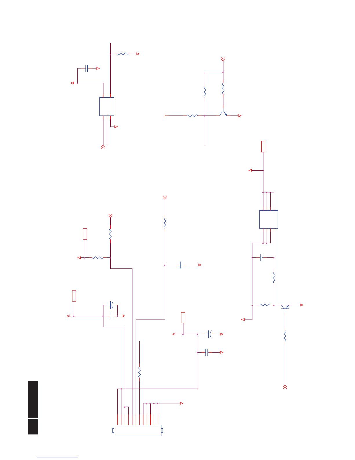
!
28
Meridian 3
Remark: Parts position can be searched by using FIND function in PDF.
+
C706
220uF 25V
C704
NC/0.1UF 16V
+
C702
220uF 25V
C707
1UF 16V
C705
100NF 25V
R702
4.7K1/16W
R710
4.7K1/16W
C703
100NF 25V
R703
100OHM
CN702
CONN
1234567891011
12
U702
AO4411
S1S2S3G
4
D8D7D6D
5
R741
10K
R704
100R 1/10W 5%
Q703
LMBT3904LT1G
R707
NC / 0R 05 1/ 10W
+3.3V 14
+5V_ON 2,5,10,11,15
+5V 7,11,12,14
GNDGND
GND +19V_ON 10,16
+5V
GND
GND
+3.3V
GND
+5V_ON
+19V_ON
+5V_ON
BL_ON 10
BL_ADJ 12
MISSION_POWER_ON11
PS_ON 11
DIM
ON/OFF
Delete Q702, R705, R706, R708 - 20121025
R707 f ro m 0_ohm chan g e t o NC - 20121025
Q705
LMBT3904LT1G
PS_ON1
R739
4.7K1/16W
GND
R738
NC/ 0R 05 1/10W
R737
10K 1/10W 5%
Add U7781, C7798, R7782 - 20121025
BL_EN3
+5V_ON
PS_ON1
SYS_POWERON
U7781
74LVC1G08GW
B1A2GND
3
Y
4
VCC
5
Change C 706 t ype - 20121025
GND
+3.3V
BL_EN
ON/OFF
BL_ON
GND
C7798
1UF 16V
R709
47K
GND
R7782
4K7 1/10W 5%
Power : Main
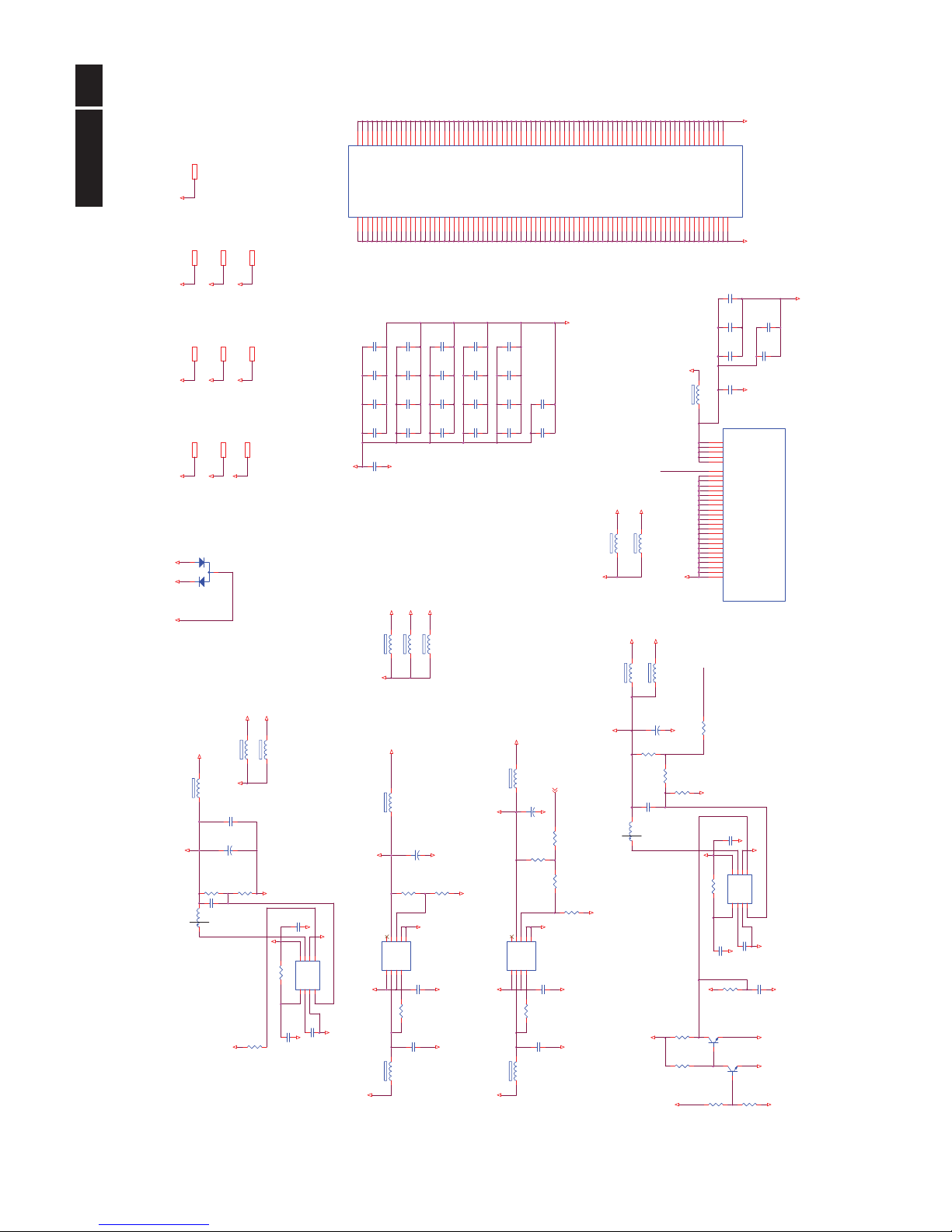
29
Meridian 3
Remark: Parts position can be searched by using FIND function in PDF.
Vout = 0.8V (1+( R1/R2Ĵ))
DC12_FB
DC12_OUT
Q708 turn on when +1.8V
power reach to 1.5V
ADJ +2.5V
Athena System Power
U401M
STDP9320
VDD1V2_DIG
K11
VDD3V3_DIG
AG7
VDD1V2_DIG
K10
VDD1V2_DIG
L10
VDD1V2_DIG
M10
VDD1V2_DIG
N10
VDD1V2_DIG
P10
VDD1V2_DIG
R10
VDD1V2_DIG
T10
VDD1V2_DIG
U10
VDD1V2_DIG
V10
VDD1V2_DIG
V11
VDD1V2_DIG
K17
VDD1V2_DIG
K18
VDD1V2_DIG
L18
VDD1V2_DIG
M18
VDD1V2_DIG
N18
VDD1V2_DIG
P18
VDD1V2_DIG
R18
VDD1V2_DIG
T18
VDD1V2_DIG
U18
VDD1V2_DIG
V18
VDD1V2_DIG
V17
VDD3V3_DIG
AG8
VDD3V3_DIG
AG9
VDD3V3_DIG
E21
VDD3V3_DIG
E22
REG_OUT_1V2
AG26
Please placement all in the same side
Athena System Ground
U401P
STDP9320
GNDA1GNDH3GNDH4GNDJ3GNDJ4GNDJ5GNDK3GNDK4GNDL3GNDL4GNDM4GNDN3GNDN4GNDP3GNDP4GNDR3GNDR4GNDR5GNDT3GNDT4GNDU4GNDV3GNDV4GNDW3GNDW4GNDY3GNDY4GND
AA3
GND
AA4
GND
AB5
GND
AC5
GND
AE3
GND
AG1
GND
AC6
GND
AC7
GND
AD7
GND
AE7
GND
AF7
GND
AD6
GND
AC8
GND
AD8
GND
AE8
GND
AF8
GND
AE6
GND
AD9
GND
AD10
GND
AE9
GND
AD11
GND
AE11
GND
AD12
GND
AE12
GND
AC12
GND
AC16
GND
AC21
GND
AC22
GNDA9GNDB9GNDC9GNDD9GNDE9GND
C10
GND
D10
GND
C11
GND
D11
GND
C12
GND
D12
GND
C13
GND
D13
GND
C14
GND
D14
GND
C15
GND
D15
GND
C16
GND
D16
GND
E16
GND
E17
GND
E18
GND
A27
GND
AG6
GND
AF6
GND
E23
GND
AD13
GND
AE13
GND
F23
GND
AF9
GND
E19
GND
E20
GND
H23
GND
AA24
GND
AB23
GND
AC23
GND
AG27
GND
K12
GND
K13
GND
K14
GND
K15
GND
K16
GND
L11
GND
L12
GND
L13
GND
L14
GND
L15
GND
L16
GND
L17
GND
M11
GND
M12
GND
M13
GND
M14
GND
M15
GND
M16
GND
M17
GND
N11
GND
N12
GND
N13
GND
N14
GND
N15
GND
N16
GND
N17
GND
P11
GND
P12
GND
P13
GND
P14
GND
P15
GND
P16
GND
P17
GND
R11
GND
R12
GND
R13
GND
R14
GND
R15
GND
R16
GND
R17
GND
T11
GND
T12
GND
T13
GND
T14
GND
T15
GND
T16
GND
T17
GND
U11
GND
U12
GND
U13
GND
U14
GND
U15
GND
U16
GND
U17
GND
V12
GND
V13
GND
V14
GND
V15
GND
V16
GND
AD5
GND
AE5
GND
AF5
GND
AE4
C731
100NF 25V
U704
G9661
POK1VEN2VIN3VPP
4
NC
5
VO
6
ADJ
7
GND
8
E-Pad
9
R716
10K 1/10W 5%
FB715
120R 6A
C708
10N 50V
FB707
120R 6A
Q704
LMBT3904LT1G
FB714
120R 6A
FB702
120R 6A
C744
10UF 10V
C719
1N 50V
FB708
120R 6A
C713
22UF 16V
C749
100NF 25V
C743
100NF 25V
FB711
120R 6A
L702
2.2uH
+
C722
100UF 16V
C752
100NF 25V
R724
10K 1/10W 5%
C740
100NF 25V
FB704
120R 6A
FB706
120R 6A
+
C736
220uF 25V
R726
10K 1/10W 5%
C750
NC/1uF 16V
C727
100NF 25V
C738
1UF 16V
+
C742
220uF 25V
C715
1N 50V
R713
10K 1/10W 5%
C745
22UF 16V
C716
100NF 25V
R729
12K 1/10W 1%
FB701
120R 6A
C720
100NF 25V
FB705
120R 6A
R712
4K7 1/10W 5%
C726
1N 50V
C732
1N 50V
R717
4K7 1/10W 5%
C718
100NF 25V
C741
10N 50V
U703
G9661
POK1VEN2VIN3VPP
4
NC
5
VO
6
ADJ
7
GND
8
E-Pad
9
FB703
120R 6A
C701
1N 50V
C725
100NF 25V
R722
12K 1/10W 1%
C717
1N 50V
R728
NC/0.05R
C739
1N 50V
C712
100NF 25V
C735
100NF 25V
R715
10K 1/10W 5%
R701
10 OHM
L701
2.2uH
D701
BAT54SH
1
2
3
R727
20K 1/10W 5%
U705
AT1528P11U
VCC1REF2GND3FB
4
EN
5
PGND
6
LX
7
VIN
8
Q701
LMBT3904LT1G
R718
10K 1/10W 5%
C730
1N 50V
R730
NC/100K
C748
100NF 25V
R719
330OHM 1/10W
C729
100NF 25V
R714
10 OHM
C747
100NF 25V
C723
1UF 16V
R725
10K 1/10W 5%
+
C709
220uF 25V
R711
14.7KOHM 1/10W
C746
1N 50V
C733
100NF 25V
R731
10K 1/10W 5%
U701
AT1528P11U
VCC1REF2GND3FB
4
EN
5
PGND
6
LX
7
VIN
8
FB712
120R 6A
C721
10UF 10V
C714
100NF 25V
R721
NC/0.05R
C710
100NF 25V
FB713
120R 6A
C724
1N 50V
C737
10UF 10V
R723
330OHM 1/10W
C728
1N 50V
C751
1N 50V
C711
10UF 10V
FB709
120R 6A
FB710
120R 6A
C734
1N 50V
+3.3V_ AUD 7
+3.3V_I/O 4,8,9,10,11,12
+5V 7,11,12, 13
+1.5V_DD R 6
+1.2V_AUD 7
+2.5V_DD R 6
+2.5V_LVDS 10
+2.5V_DD R
+1.2V_DPTX 9
+2.5V_ DPTX 9
+3.3V 13
GND
GND
+3.3V
+3.3V_AUD
+5V
+1.2V_CORE
GND
GND
+2.5V_DPTX +2.5V_L VDS+1.2V_AUD
+1.5V_DD R
GND
+3.3V_I /O
+3.3V_I/O
+3.3V_SW
GND
GND
+3.3V
+3.3V_AUD
+2.5V_DDR
+2.5V_ DPTX
+2.5V_ LVDS
GND
GND
+1.5V_DDR
+3.3V_SW
+2.5V_SW
+3.3V
+1.2V_C ORE
+1.2V_SW
GND
+3.3V_ SW +1.2V_CORE
GNDGND
+1.2V_AUD
+1.2V_SW
+2.5V
+1.5V_DD R
GND
+3.3V_I/O
GND
+1.2V_CORE
GND
+5V
+5V
+5V
GND
+3.3V
+2.5V_ SW
+5V
+5V +1.5V
GNDGND
GND
GNDGND
GND
GND
GND
+1.5V
+2.5V
GND
GND
+1.2V
+5V
GND
GND
GND
GND
REG_OUT_VDD R 6
+1.2V_D PTX
+1.2V_DPTX
GND
C764
10UF 10V
REG_OUT_1V2
Mission:
1.2V: 1490m A
2.5V: 220m A
3.3V: 280m A
1.8V(V DDR): 7 70m A
LPM:
1.2V: 540m A
2.5V: 170m A
3.3V: 215m A
DC12_EN
Vo=0.8*(1+(R1/R2))
DROPOUT 0.3V@2A
ADJ +1.8V
1.2V: 1490m A
1.8V(VDDR): 770m A
220mA
ADJ +1.2V
REG_OUT_1V2
R720
11K 1/10W 1%
Enable min 2V
Cancel U705
Power Se que ncing Diode
Vout = 0.8V (1+( R1/R2Ĵ))
AT1528P11U: Max:2A
DROPOUT 0.3V@2A
Vo=0.8*(1+(R1/R2))
DC12_VCC
DC12_REF
AT1528P11U: Max:2A
Power: 3.3/2.5/1.8/1.2 V
!
30
Meridian 3
Remark: Parts position can be searched by using FIND function in PDF.
ADJ +1.2V
R734
10K 1/10W 5%
FB717
120R 6A
R733
4K7 1/10W 5%
C758
100NF 25V
FB722
120R 6A
C763
100NF 25V
FB718
120R 6A
+
C757
100UF 16V
FB724
120R 6A
FB721
120R 6A
U707
AP2127K-ADJTRG1
IN1GND2SHDN
3
SET
4
OUT
5
FB723
120R 6A
FB719
120R 6A
C756
100NF 25V
U708
G9661
POK1VEN2VIN3VPP
4
NC
5
VO
6
ADJ
7
GND
8
E-Pad
9
FB720
120R 6A
C755
100NF 25V
+
C759
100UF 16V
+
C754
100UF 16V
C762
1UF 16V
+
C761
100UF 16V
FB725
120R 6A
R735
10K 1/10W 5%
R736
20K 1/10W 5%
FB716
120R 6A
C760
10UF 10V
R732
10K 1/10W 5%
+
C753
100UF 16V
+3.3V_LPM 5,11
+5V_ON 2,5,10,11,13
+1.2V_LPM 11
+2.5V_LPM_ADC 2
+2.5V_LPM 11
+3.3V_L PM_C OMBO 4, 5
+1.2V_LPM_AD C
+3.3V_L PM_C OMBO
+1.2V_L PM_C OMBO 4
+1.2V_LPM_ADC 2
+3.3V_ LPM
+5V_ON
+1.2V_LPM
+2.5V_LPM_ADC
+3.3V_L PM_C OMBO
+1.2V_LPM_ADC
+1.2V_L PM_C OMBO
+2.5V_LPM
+3.3V_LPM_POW ER
+1.2V_LPM
+5V_ON
+3.3V_ LPM
+3.3V_LPM_POWER
+2.5V_LPM_POWER
+1.2V_L PM_C OMBO
GND
GND
+2.5V_LPM
+2.5V_LPM_ADC
GND
GND
GNDGNDGND
+5V_ON
GND
+2.5V_LPM_POWER
U706
uP0113CHA3-33
VOUT
2
VIN
3
GND
1
DROPOUT 0.3V@2A
Vo=0.8*(1+(R1/R2))
Inportant Power Sequence :
+3.3V_LPM --> + 2.5V_LPM --> +1.2V_LPM --
--> +3.3V_SW --> +2.5V_SW --> +1.8V_DDR --
--> +1.2V_CORE/SW
Vo=0.8*(1+(R1/R2))
170mA
ADJ +2.5V
ULTRA LOW DROPOUT 0.4V@300mA
Fixed +3.3V
215mA
540mA
Power : LPM
 Loading...