

Philips 28L202A1B, 28L202A1A Datasheet

SC28L202
Dual universal asynchronous
receiver/transmitter (DUART)
Objective specification
IC19 Data Handbook
1998 Oct 05
INTEGRATED CIRCUITS

Philips Semiconductors Objective specification
SC28L202
Dual universal asynchronous receiver/transmitter
(DUART)
Designed for “Glueless operation in 68XXX and X86 environments”
2
1998 Oct 05
DESCRIPTION
The 28L202 is a high performance functional upgrade for the Philips
dual channel UARTS. The SCC2692 and SC26C92 operating at 3.3
or 5 volts supply with added features and deeper partitioned FIFOs.
Its configuration on power up is similar that of the SC26C92. Its
differences from the SC26C92 are: 256 character receiver, 256
character transmit FIFOs, CRC error detection, 3 and 5 volt
compatibility, 8 I/O ports for each UART. IRDA compatibility,
arbitrating interrupt system and overall faster buss and data speeds.
It is fabricated in an advanced CMOS process that allows stand by
current of less that one microampere.
Pin programming will allow the device to operate with either the
Motorola or Intel bus interface by changing the function of some
pins. (Reset is inverted, DACKN enabled for example).
The Philips Semiconductors 28L202 Dual Universal Asynchronous
Receiver/Transmitter (DUART) is a single-chip CMOS–LSI
communications device that provides two full-duplex asynchronous
receiver/transmitter channels in a single package. It interfaces
directly with microprocessors and may be used in a polled or
interrupt driven system.
The operating mode and data format of each channel can be
programmed independently. Additionally, each receiver and
transmitter can select its operating speed as one of twenty-three
fixed baud rates; a 16X clock derived from a programmable
counter/timer, or an external 1X or 16X clock. The baud rate
generator and counter/timer can operate directly from a crystal or
from external clock inputs. The ability to independently program the
operating speed of the receiver and transmitter make the DUART
particularly attractive for dual-speed channel applications such as
clustered terminal systems.
Each receiver and transmitter is buffered by eight character FIFOs
to minimize the potential of receiver overrun, transmitter underrun
and to reduce interrupt overhead in interrupt driven systems. In
addition, a flow control capability is provided to disable a remote
transmitter when the receiver buffer is full.
Also provided on the 28L202 are a multipurpose 7-bit input port and
a multipurpose 8-bit output port. These can be used as
general-purpose I/O ports or can be assigned specific functions
(such as clock inputs or status/interrupt outputs) under program
control.
The 28L202 are available in two package versions: a 44-pin PLCC
and 44-pin plastic quad flat pack (PQFP).
FEA TURES
•3.3 or 5.0 volt operation
•Dual full-duplex independent asynchronous receiver/transmitters
•256 or larger character FIFOs for each receiver and transmitter
•Power up as 8 bit data no parity one stop bit 9600 baud
•Pin programming (PQFP package) to 68K or 80xxx bus interface
•Programmable data format
– 5 to 8 data bits plus parity
– Odd, even, no parity or force parity
– 1, 1.5 or 2 stop bits programmable in 1/16-bit increments
•16-bit programmable Counter/Timer
•Programmable baud rate for each receiver and transmitter
selectable from:
– 23 fixed rates: 50 to 230.4k baud
– Other baud rates to MHz at 16X
– Programmable user-defined rates derived from a
programmable Counter/timer
– External 1X or 16X clock
•Parity, framing, and overrun error detection
•False start bit detection
•Line break detection and generation
•Programmable channel mode
– Normal (full-duplex)
– Automatic echo
– Local loop back
– Remote loop back
– Multi-drop mode (also called ‘wake-up’ or ‘9-bit’)
•Multi-function 7-bit input port
– Can serve as clock or control inputs
– Change of state detection on eight inputs
– Inputs have typically >100k pull-up resistors
•Multi-function 8-bit output port
– Individual bit set/reset capability
– Outputs can be programmed to be status/interrupt signals
•Versatile interrupt system
– Single interrupt output with eight maskable interrupting
conditions
– Output port can be configured to provide a total of up to six
separate interrupt outputs that may be wire ORed.
– Each FIFO can be programmed for four different interrupt
levels.
– Watch dog timer for each receiver
•Maximum data transfer rates:
– 1X – 1Mb/sec, 16X – 1Mb/sec
•Automatic wake-up mode for multi-drop applications
•Start-end break interrupt/status
•Detects break which originates in the middle of a character
•On-chip crystal oscillator
•Power down mode
•Receiver time-out mode
•Single +3.3V or +5V power supply
•Powers up to emulate SCC2692 and SC26C92

Philips Semiconductors Objective specification
SC28L202
Dual universal asynchronous receiver/transmitter
(DUART)
1998 Oct 05
3
ORDERING INFORMATION
ББББББББББББ
Á
ББББББББББББ
Á
DESCRIPTION
БББББББББ
Á
БББББББББ
Á
INDUSTRIAL
V
CC
= +3.3 +5V ±10%,
T
A
= –40 TO +85C
БББББББББ
Á
БББББББББ
Á
DRAWING NUMBER
44-Pin Plastic Leaded Chip Carrier (PLCC)
28L202A1A
SOT187–2
44-Pin Plastic Quad Flat Pack (PQFP)
28L202A1B
SOT307–2

Philips Semiconductors Objective specification
SC28L202
Dual universal asynchronous receiver/transmitter
(DUART)
1998 Oct 05
4
PIN CONFIGURATION DIAGRAM
PIN FUNCTION PIN FUNCTION
1NC 27D2
2A0 28D0
3 I/OB3 29 I/OA6
4 A1 30 I/OA4
5 I/OB1 31 I/OA2
6 A2 32 I/OA0
7 A3 33 TxDA
8 I/OB0 34 NC
9 WRN 35 RxDA
10 RDN 36 X1/CLK
11 RxDB 37 X2
12 I/M 38 RESET
13 TxDB 39 CEN
14 I/OA1 40 I/OB2
15 I/OA3 41 I/OB6
16 I/OA5 42 I/OB5
17 I/OA7 43 I/OB4
18 D1 44 V
CC
19 D3 45 A4
20 D5 46 A5
21 D7 47 I/OB7
22 V
SS
48 PRE
23 NC 49 V
CC
24 INTRN 50 V
SS
25 D6 51 NC
26 D4 52 NC
1
46
20
33
47
34
21
8
PLCC
7
TOP VIEW
INDEX
CORNER
SD00680

Philips Semiconductors Objective specification
SC28L202
Dual universal asynchronous receiver/transmitter
(DUART)
1998 Oct 05
5
PIN CONFIGURATION DIAGRAM
PIN FUNCTION PIN FUNCTION
1NC 27D2
2A0 28D0
3 I/OB3 29 I/OA6
4 A1 30 I/OA4
5 I/OB1 31 I/OA2
6 A2 32 I/OA0
7 A3 33 TxDA
8 I/OB0 34 NC
9 R/WN 35 RxDA
10 DACKN 36 X1/CLK
11 RxDB 37 X2
12 I/M 38 RESETN
13 TxDB 39 CEN
14 I/OA1 40 I/OB2
15 I/OA3 41 IACKN
16 I/OA5 42 I/OB5
17 I/OA7 43 I/OB4
18 D1 44 V
CC
19 D3 45 A4
20 D5 46 A5
21 D7 47 I/OB7
22 V
SS
48 PRE
23 NC 49 V
CC
24 INTRN 50 V
SS
25 D6 51 NC
26 D4 52 NC
1
46
20
33
47
34
21
8
PLCC
7
TOP VIEW
INDEX
CORNER
SD00681
Philips Semiconductors Objective specification
SC28L202
Dual universal asynchronous receiver/transmitter
(DUART)
1998 Oct 05
6
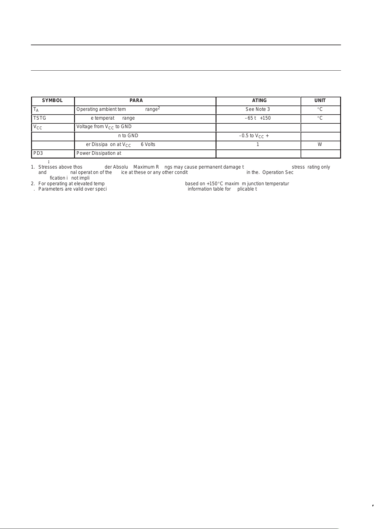
ABSOLUTE MAXIMUM RATINGS
1
SYMBOL
PARAMETER
RATING
БББББ
UNIT
T
A
Operating ambient temperature range
2
See Note 3
БББББ
C
TSTG
Storage temperature range
–65 to +150
БББББ
C
V
CC
Voltage from VCC to GND
4
–0.5 to +7.0
БББББ
V
V
SS
Voltage from any pin to GND
–0.5 to VCC + 0.5
БББББ
V
PD5
Power Dissipation at VCC = 5.6 Volts
1
БББББ
W
PD3
Power Dissipation at VCC = 3.3 Volts
0.5
БББББ
W
NOTES:
1. Stresses above those listed under Absolute Maximum Ratings may cause permanent damage to the device. This is a stress rating only
and the functional operation of the device at these or any other conditions above those indicated in the. Operation Section of this
specification is not implied.
2. For operating at elevated temperatures, the device must be derated based on +150C maximum junction temperature.
3. Parameters are valid over specified temperature range. See ordering information table for applicable temperature range and operating
supply range.
4. This product includes circuitry specifically designed for the protection of its internal devices from damaging effects of excessive static
charge. Nonetheless, it is suggested that conventional precautions be taken to avoid applying any voltages larger than the rated maxim.
Philips Semiconductors Objective specification
SC28L202
Dual universal asynchronous receiver/transmitter
(DUART)
1998 Oct 05
7
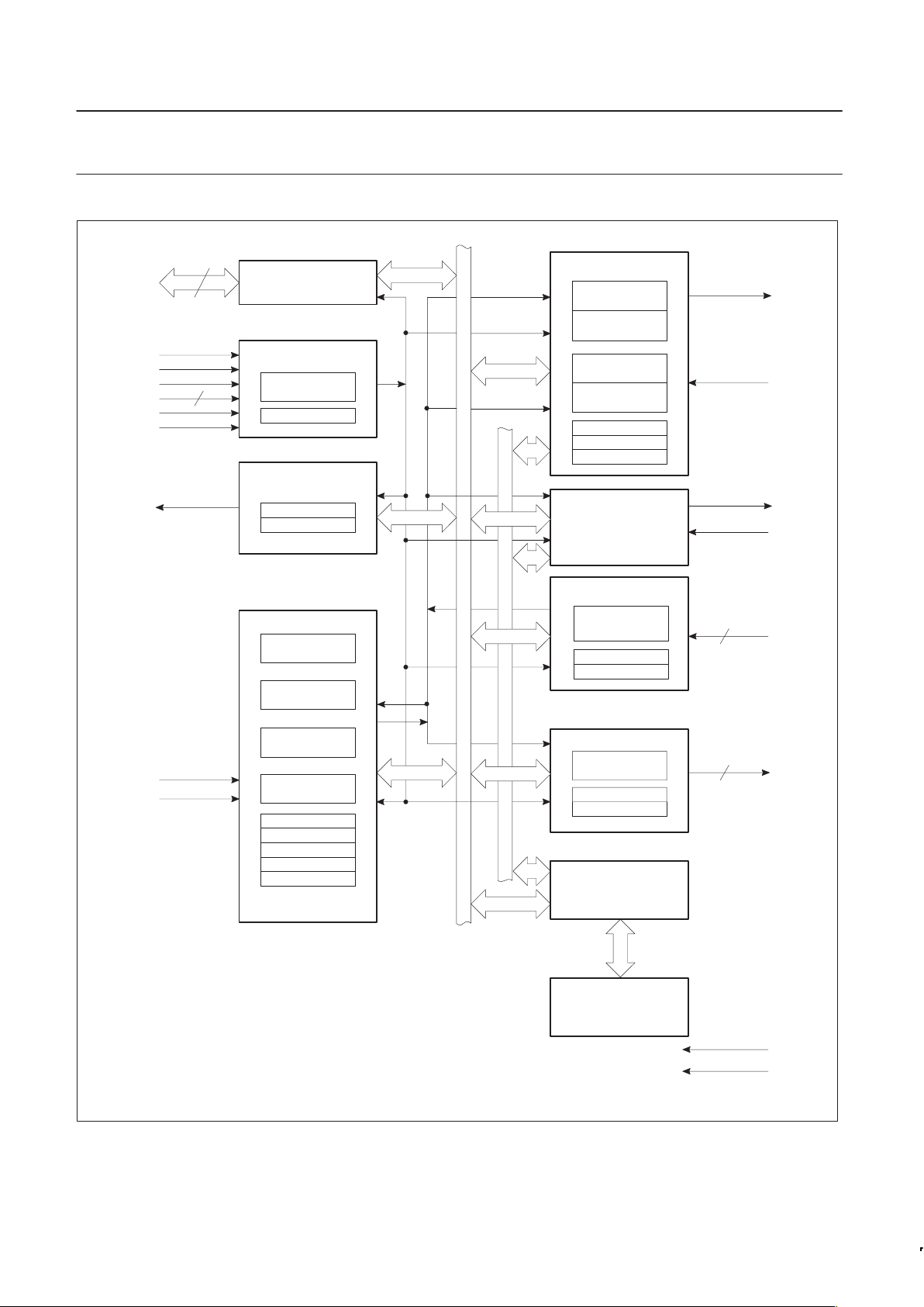
8
D0–D7
RDN
WRN
CEN
A0–A5
RESET
INTRN
X1/CLK
X2
4
BUS BUFFER
OPERATION CONTROL
ADDRESS
DECODE
R/W CONTROL
INTERRUPT CONTROL
IMR
ISR
TIMING
BAUD RATE
GENERATOR
CLOCK
SELECTORS
COUNTER/
TIMER
XTAL OSC
CSRA
CSRB
ACR
CTLR
CHANNEL A
TRANSMIT
HOLDING REG
TRANSMIT
SHIFT REGISTER
RECEIVE
HOLDING REG (3)
RECEIVE
SHIFT REGISTER
MRA1, 2
CRA
SRA
I/O PORT A
CHANGE OF
STATE
DETECTORS (4)
I/O PORT B
FUNCTION
SELECT LOGIC
OPCR
TxDA
RxDA
I/O7:0A
I/O7:0B
V
CC
GND
CONTROL
TIMING
INTERNAL DATABUS
CHANNEL B
(AS ABOVE)
IPCR
ACR
OPR
CTLR
U
RxDB
TxDB
8
8
SD00679
FIFO
RAM
FIFO DATABUS
FIFO
CONTROL
I/M
Figure 1. Block Diagram
Philips Semiconductors Objective specification
SC28L202
Dual universal asynchronous receiver/transmitter
(DUART)
1998 Oct 05
8
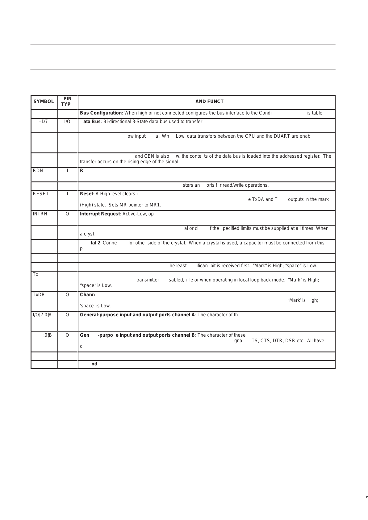
PIN CONFIGURATION FOR 80XXX BUS INTERFACE (INTEL)
ÁÁ
Á
SYMBOL
Á
Á
PIN
TYPE
БББББББББББББББББББББББББББ
Á
NAME AND FUNCTION
I/M
I
Bus Configuration: When high or not connected configures the bus interface to the Conditions shown in this table.
D0–D7
I/O
Data Bus: Bi-directional 3-State data bus used to transfer commands, data and status between the DUART and the
CPU. D0 is the least significant bit.
ÁÁ
Á
ÁÁ
Á
CEN
Á
Á
Á
Á
I
БББББББББББББББББББББББББББ
Á
БББББББББББББББББББББББББББ
Á
Chip Enable: Active-Low input signal. When Low, data transfers between the CPU and the DUART are enabled on
D0–D7 as controlled by the WRN, RDN and A0–A3 inputs. When High, places the D0–D7 lines in the 3-State condition.
WRN
I
Write Strobe: When Low and CEN is also Low, the contents of the data bus is loaded into the addressed register. The
transfer occurs on the rising edge of the signal.
ÁÁ
Á
RDN
Á
Á
I
БББББББББББББББББББББББББББ
Á
Read Strobe: When Low and CEN is also Low, causes the contents of the addressed register to be presented on the
data bus. The read cycle begins on the falling edge of RDN.
A0–A3
I
Address Inputs: Select the DUART internal registers and ports for read/write operations.
ÁÁ
Á
RESET
Á
Á
I
БББББББББББББББББББББББББББ
Á
Reset: A High level clears internal registers (SRA, SRB, IMR, ISR, OPR, OPCR), puts OP0 – OP7 in the High state,
stops the counter/timer, and puts Channels A and B in the inactive state, with the TxDA and TxDB outputs in the mark
(High) state. Sets MR pointer to MR1.
INTRN
O
Interrupt Request: Active-Low, open-drain, output which signals the CPU that one or more of the eight maskable interrupting conditions are true.
ÁÁ
Á
X1/CLK
Á
Á
I
БББББББББББББББББББББББББББ
Á
Crystal 1: Crystal or external clock input. A crystal or clock of the specified limits must be supplied at all times. When
a crystal is used, a capacitor must be connected from this pin to ground (see Figure 7).
ÁÁ
Á
X2
Á
Á
O
БББББББББББББББББББББББББББ
Á
Crystal 2: Connection for other side of the crystal. When a crystal is used, a capacitor must be connected from this
pin to ground (see Figure 7). If X1/CLK is driven from an external source, this pin must be left open.
RxDA
I
Channel A Receiver Serial Data Input: The least significant bit is received first. “Mark” is High; “space” is Low.
RxDB
I
Channel B Receiver Serial Data Input: The least significant bit is received first. “Mark” is High; “space” is Low.
ÁÁ
Á
ÁÁ
Á
TxDA
Á
Á
Á
Á
O
БББББББББББББББББББББББББББ
Á
БББББББББББББББББББББББББББ
Á
Channel A Transmitter Serial Data Output: The least significant bit is transmitted first. This output is held in the
“mark” condition when the transmitter is disabled, idle or when operating in local loop back mode. “Mark” is High;
“space” is Low.
ÁÁ
Á
TxDB
Á
Á
O
БББББББББББББББББББББББББББ
Á
Channel B Transmitter Serial Data Output: The least significant bit is transmitted first. This output is held in the
‘mark’ condition when the transmitter is disabled, idle, or when operating in local loop back mode. ‘Mark’ is High;
‘space’ is Low.
ÁÁ
Á
I/O[7:0]A
Á
Á
O
БББББББББББББББББББББББББББ
Á
General-purpose input and output ports channel A: The character of these pins is controlled by I/OPCR. They may
be inputs or outputs and will present many internal clocks and interrupt signals: RTS, CTS, DTR, DSR etc. All have
change of state detectors and the input is always active.
ÁÁ
Á
I/O[7:0}B
Á
Á
O
БББББББББББББББББББББББББББ
Á
General-purpose input and output ports channel B: The character of these pins is controlled by I/OPCR. They may
be inputs or outputs and will present many internal clocks and interrupt signals: RTS, CTS, DTR, DSR etc. All have
change of state detectors and the input is always active.
V
CC
Pwr
Power Supply: +3.3 or +5V supply input 10%
GND
Pwr
Ground
Philips Semiconductors Objective specification
SC28L202
Dual universal asynchronous receiver/transmitter
(DUART)
1998 Oct 05
9
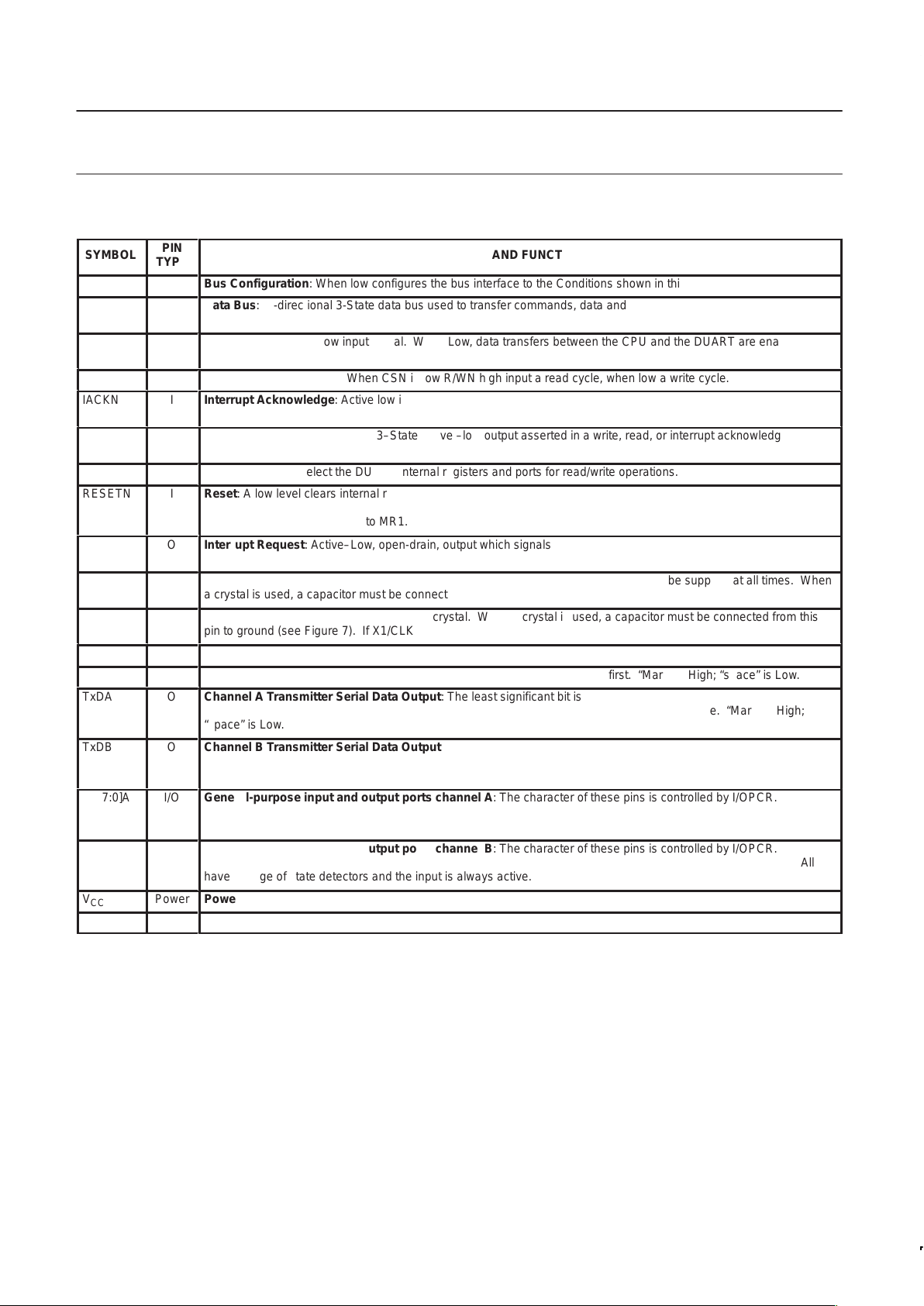
PIN CONFIGURATION FOR 68XXX BUS INTERFACE (INTEL)
ÁÁ
Á
SYMBOL
Á
Á
PIN
TYPE
БББББББББББББББББББББББББББ
Á
NAME AND FUNCTION
I/M
I
Bus Configuration: When low configures the bus interface to the Conditions shown in this table.
D0–D7
I/O
Data Bus: Bi-directional 3-State data bus used to transfer commands, data and status between the DUART and the
CPU. D0 is the least significant bit.
ÁÁ
Á
CSN
Á
Á
I
БББББББББББББББББББББББББББ
Á
Chip Enable: Active-Low input signal. When Low, data transfers between the CPU and the DUART are enabled on
D0–D7 as controlled by the R/WN and A0–A3 inputs. When High, places the D0–D7 lines in the 3-State condition.
R/WN
I
Read/Write: Input Signal. When CSN is low R/WN high input a read cycle, when low a write cycle.
ÁÁ
Á
IACKN
Á
Á
I
БББББББББББББББББББББББББББ
Á
Interrupt Acknowledge: Active low input indicates an interrupt acknowledge cycle. Usually asserted by the CPU in
response to an interrupt request. When asserted places the interrupt vector on the bus and asserts DACKN.
DACKN
O
Data Transfer Acknowledge: A3–State active –low output asserted in a write, read, or interrupt acknowledge cycle to
indicate proper transfer of data between the CPU and the DUART.
A0–A3
I
Address Inputs: Select the DUART internal registers and ports for read/write operations.
ÁÁ
Á
RESETN
Á
Á
I
БББББББББББББББББББББББББББ
Á
Reset: A low level clears internal registers (SRA, SRB, IMR, ISR, OPR, OPCR), puts OP0–OP7 in the High state,
stops the counter/timer, and puts Channels A and B in the inactive state, with the TxDA and TxDB outputs in the mark
(High) state. Sets MR pointer to MR1.
ÁÁ
Á
INTRN
Á
Á
O
БББББББББББББББББББББББББББ
Á
Interrupt Request: Active–Low, open-drain, output which signals the CPU that one or more of the eight maskable
interrupting conditions are true.
X1/CLK
I
Crystal 1: Crystal or external clock input. A crystal or clock of the specified limits must be supplied at all times. When
a crystal is used, a capacitor must be connected from this pin to ground (see Figure 7).
ÁÁ
Á
X2
Á
Á
O
БББББББББББББББББББББББББББ
Á
Crystal 2: Connection for other side of the crystal. When a crystal is used, a capacitor must be connected from this
pin to ground (see Figure 7). If X1/CLK is driven from an external source, this pin must be left open.
RxDA
I
Channel A Receiver Serial Data Input: The least significant bit is received first. “Mark” is High; “space” is Low.
RxDB
I
Channel B Receiver Serial Data Input: The least significant bit is received first. “Mark” is High; “space” is Low.
ÁÁ
Á
TxDA
Á
Á
O
БББББББББББББББББББББББББББ
Á
Channel A Transmitter Serial Data Output: The least significant bit is transmitted first. This output is held in the
“mark” condition when the transmitter is disabled, idle or when operating in local loop back mode. “Mark” is High;
“space” is Low.
ÁÁ
Á
TxDB
Á
Á
O
БББББББББББББББББББББББББББ
Á
Channel B Transmitter Serial Data Output: The least significant bit is transmitted first. This output is held in the
‘mark’ condition when the transmitter is disabled, idle, or when operating in local loop back mode. ‘Mark’ is High;
‘space’ is Low.
ÁÁ
Á
I/O[7:0]A
Á
Á
I/O
БББББББББББББББББББББББББББ
Á
General-purpose input and output ports channel A: The character of these pins is controlled by I/OPCR. They
may be inputs or outputs and will present many internal clocks and interrupt signals: RTS, CTS, DTR, DSR etc. All
have change of state detectors and the input is always active.
ÁÁ
Á
ÁÁ
Á
I/O[7:0]B
Á
Á
Á
Á
I/O
БББББББББББББББББББББББББББ
Á
БББББББББББББББББББББББББББ
Á
General-purpose input and output ports channel B: The character of these pins is controlled by I/OPCR. They
may be inputs or outputs and will present many internal clocks and interrupt signals: RTS, CTS, DTR, DSR etc. All
have change of state detectors and the input is always active.
V
CC
Power
Power Supply: +3.3 or +5V supply input 10%
V
SS
Power
Ground
Philips Semiconductors Objective specification
SC28L202
Dual universal asynchronous receiver/transmitter
(DUART)
1998 Oct 05
10
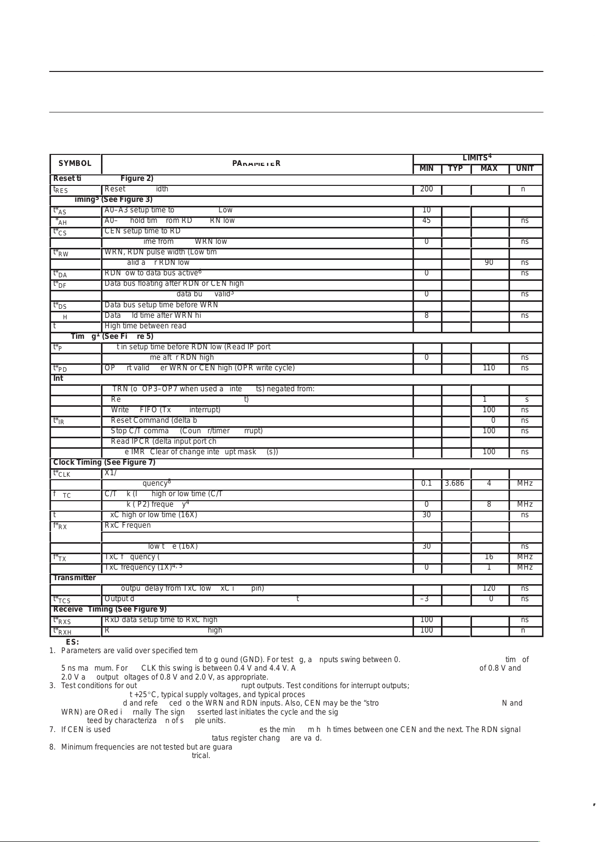
AC CHARACTERISTICS
1, 2, 3
LIMITS
4
SYMBOL
PARAMETER
MIN
TYP
MAX
ÁÁÁ
UNIT
Reset timing (See Figure 2)
t
RES
Reset Pulse Width
200
ÁÁÁ
ns
Bus Timing5 (See Figure 3)
t*
AS
A0–A3 setup time to RDN, WRN Low
10
ÁÁÁ
ns
t*
AH
A0–A3 hold time from RDN, WRN low
45
ns
t*
CS
CEN setup time to RDN, WRN low
0
ÁÁÁ
ns
t*
CH
CEN Hold time from RDN WRN low
0
ÁÁÁ
ns
t*
RW
WRN, RDN pulse width (Low time)
110
ns
t*
DD
Data valid after RDN low
90
ÁÁÁ
ns
t*
DA
RDN low to data bus active
6
0
ÁÁÁ
ns
t*
DF
Data bus floating after RDN or CEN high
30
ÁÁÁ
ns
t*
DI
RDN or CEN high to data bus invalid
3
0
ns
t*
DS
Data bus setup time before WRN or CEN high (write cycle)
75
ÁÁÁ
ns
t*
DH
Data hold time after WRN high
8
ÁÁÁ
ns
t*
RWD
High time between read and/or write cycles
1, 7
55
ns
Port Timing1 (See Figure 5)
t*
PS
Port in setup time before RDN low (Read IP ports cycle)
0
ÁÁÁ
ns
t*
PH
Port in hold time after RDN high
0
ns
t*
PD
OP port valid after WRN or CEN high (OPR write cycle)
110
ÁÁÁ
ns
Interrupt Timing (See Figure 6)
INTRN (or OP3–OP7 when used as interrupts) negated from:
ÁÁÁ
Read RxFIFO (RxRDY/FFULL interrupt)
100
ns
Write TxFIFO (TxRDY interrupt)
100
ÁÁÁ
ns
t*
IR
Reset Command (delta break change interrupt)
100
ÁÁÁ
ns
Stop C/T command (Counter/timer interrupt)
100
ns
Read IPCR (delta input port change interrupt)
100
ÁÁÁ
ns
Write IMR (Clear of change interrupt mask bit(s))
100
ÁÁÁ
ns
Clock Timing (See Figure 7)
t*
CLK
X1/CLK high or low time
80
ÁÁÁ
ns
f*
CLK
X1/CLK frequency
8
0.1
3.686
4
ÁÁÁ
MHz
f*
CTC
C/T Clk (IP2) high or low time (C/T external clock input)
55
ÁÁÁ
ns
f*
CTC
C/T Clk (IP2) frequency
4
0
8
MHz
t*
RX
RxC high or low time (16X)
30
ÁÁÁ
ns
f*
RX
RxC Frequency (16X)
0
16
ÁÁÁ
MHz
RxC Frequency (1x)
4, 9
0
1
MHz
t*
TX
TxC High or low time (16X)
30
ÁÁÁ
ns
f*
TX
TxC frequency (16X)
16
ÁÁÁ
MHz
TxC frequency (1X)
4, 5
0
1
ÁÁÁ
MHz
Transmitter Timing (See Figure 8)
t*
TXD
TxD output delay from TxC low (TxC input pin)
120
ÁÁÁ
ns
t*
TCS
Output delay from TxC output pin low to TxD data output
–30
30
ÁÁÁ
ns
Receiver Timing (See Figure 9)
t*
RXS
RxD data setup time to RxC high
100
ÁÁÁ
ns
t*
RXH
RxD data hold time from RxC high
100
ÁÁÁ
ns
NOTES:
1. Parameters are valid over specified temperature range.
2. All voltage measurements are referenced to ground (GND). For testing, all inputs swing between 0.4 V and 3.0 V with a transition time of
5 ns maximum. For X1/CLK this swing is between 0.4 V and 4.4 V . All time measurements are referenced at input voltage of 0.8 V and
2.0 V and output voltages of 0.8 V and 2.0 V , as appropriate.
3. Test conditions for outputs; C
L
= 150 pF, except interrupt outputs. Test conditions for interrupt outputs; CL = 50 pF, RL = 2.7 Kohm to VCC.
4. Typical values are at +25C, typical supply voltages, and typical processing parameters.
5. Timing is illustrated and referenced to the WRN and RDN inputs. Also, CEN may be the “strobing” input. CEN and RDN (also CEN and
WRN) are ORed internally. The signal asserted last initiates the cycle and the signal negated first terminates the cycle.
6. Guaranteed by characterization of sample units.
7. If CEN is used as the “strobing” input, the parameter defines the minimum high times between one CEN and the next. The RDN signal must
be negated for t
RWD
to guarantee that any status register changes are valid.
8. Minimum frequencies are not tested but are guaranteed by design.
9. Clocks for 1X mode should be symmetrical.

Philips Semiconductors Objective specification
SC28L202
Dual universal asynchronous receiver/transmitter
(DUART)
1998 Oct 05
11
OVER ALL DESCRIPTION
The SC28L202 is composed of several functional blocks. They are
listed in the approximate order of hierarchy as seen from the pins of
the device.
•Timing Circuits
•Bus interface. 68K or x86 format
•I/O Ports
•UARTS
•Arbitrating Interrupt Structure
•Character & Address Recognition
•Variable FIFO Partition Structure
•Test Modes and Boundary Scan
BRIEF DESCRIPTION OF FUNCTIONAL BLOCKS
Timing Circuits
Crystal Oscillator
The crystal oscillator is the main timing element for the 28L202. It is
nominally set at 14.7456 MHz and may be used to 29.4912 MHz.
The use of an external clock allows all frequencies to 40 MHz.
BRG
The BRG is the baud rate generator, is driven by the crystal input
and generated all of the 24 “fixed” internal baud rates.
Counter-Timer .
The counter-timer provides miscellaneous baud rated, timing
periods and acts as an extra watchdog timer for the for the
receivers. It has 8 clock sources.
Bus Interface
The bus interface operates in “68K” or “x86” format as selected by
the I/M pin. The signals used by this section are the Address, Data
bus, Chip select, read/write, Data acknowledge and Interrupt
acknowledge and Interrupt request. Assertion of DACKN requires
two edges of the X1clk after the assertion of CEN.
I/O ports
Each UART is provided with 8 I/O ports. Each port is equipped with
a change of state detector. The input circuit of these pins is always
active. Under program control the ports my display internal signals
or static logic levels. The functions represented by the I/O ports
include hardware flow control. Modem signals, signals for interrupt
conditions or various internal clocks and timing intervals. Noisy
inputs to the I/O ports are filtered (de-bounced) by a 38.4 KHz clock.
UARTS
The uarts are fully independent, full duplex and provide all normal
asynchronous functions: 5 to 8 data bits, parity odd or even,
programmable stop bit length, false start bit detection. Also
provided are 256 byte FIFOs Xon/Xoff software flow control and
IRDA pulse modulation. The BRG, Counter-timer, or external clocks
provide the baud rates. The receivers and transmitters may operate
in either the “1x” or “16x” modes.
Interrupt Arbitration
The interrupt system uses a highly programmable arbitrating
technique to establish when an interrupt should be presented to the
processor. The advantageous feature of this system is the
presentation of the context of the interrupt. It is presented in both a
current interrupt register and in the interrupt vector. The context of
the interrupt shows the interrupting channel, identifies which of the 8
possible sources in requesting interrupt service and in the case of a
receiver or transmitter gives the current fill level of the FIFO.
The content of the current interrupt register also drives the Global
Registers of the interrupt system. These registers are indirect
addresses (pointers) to the fields describing the internal source
requesting interrupt service.
Programming of Bid Control Registers allows the interrupt level of
any source to be varied at any time over a range of 256 levels.
Character and Address Recognition
The character recognition system is designed as a general system.
There is one for each UART. Each recognition block stores up to
three characters. The recognition is done on a byte boundary and
sets status and interrupt when an recognition event occurs. Each
has four modes of operation.
A subset of the recognition system is Xon/Xoff character recognition
and multi-drop address recognition. If Xon/Xoff or multi-dorp
function is enabled the recognition system passes the information
about the recognition event to the appropriate receiver or transmitter
state machine for execution. In any case the information about a
recognition event is available to the interrupt system and to the
control processor.
FIFO Partitioning and Control
The FIFO memory is implemented in ram. Nominally 1000 bytes of
ram are divided between the four FIFOs of the DUART. The default
partition is 256 (0xFF) bytes for each fifo. Under program control
size of the partition for any a particular FIFO may be varied from 1 to
1024.
The interrupt level for each FIFO is also under program control and
is continuously variable through out the range of the partition. A
small processor controls all of the FIFO reading, writing, interrupting,
flow control signaling, and status reporting.
Test Modes
Three test modes are provided to verify UART function and
processor interface integrity . These are Auto echo, Local Loop
Back, and Remote Loop Back. Through local loop back the
software developer may verify all of the interrupt, flow control; the
hardware designer verifies all of the timing and pin connections. This
information is obtained without any recourse to external test
equipment or terminals.
Boundary scan provides verification of manufacturing process and
to a lesser extent identifies damage that may occur to pins due to
electrical over stress or electrostatic discharge.
DET AILED DESCRIPTIONS
NOTE: For the convenience of the reader some paragraphs in the
following section will be repeated in descriptions of closely linked
functions.
Timing Circuits
Crystal Oscillator
The crystal oscillator operates directly from a crystal, tuned between
14.7456 MHz and 29 4912 MHz connected across the X1/CCLK and
X2 inputs with a minimum of external components. BRG values
listed for the clock select registers correspond to a 14.7456 MHz

Philips Semiconductors Objective specification
SC28L202
Dual universal asynchronous receiver/transmitter
(DUART)
1998 Oct 05
12
crystal frequency. Use of different frequencies will change the
“standard” baud rates by precisely the ratio of 14.7456 to the
different crystal.
An external clock up to 40 MHz frequency range may be connected
to X1/CCLK. If an external clock is used instead of a crystal,
X1/CCLK must be driven and X2 left floating. The X1 clock serves
as the basic timing reference for the baud rate generator (BRG) and
is available to the BRG timers, counter-timers, and control logic.
Baud Rate Generator BRG
The baud rate generator operates from the oscillator or external
X1/CCLK clock input and generates 24 commonly used data
communications baud rates (including MIDDI) ranging from 50 to
230.4K baud. These common rates may be doubled (up to 460.8
and 1500K baud) when faster clocks are used on the X1/X2 clock
inputs. (See Receiver and Transmitter Clock Select Register
descriptions.) All of these are available simultaneously for use by
any receiver or transmitter. The clock outputs from the BRG are at
16X the actual baud rate.
Counter-Timer
The two Counter/Timers are programmable 16 bit dividers that are
used for generating miscellaneous clocks or generating timeout
periods. These clocks may be used by any or all of the receivers
and transmitters in the DUART or may be directed to an I/O pin for
external use.
Counter/Timer programming
The counter timer is a 16-bit programmable divider that operates in
one of five modes: character count, pulse mode, counter, timer, and
time out. Character count counts characters. The pulse mode
generates a periodic pulse of one clock period in width. The timer
mode it generates a square wave. In the counter mode it generates
a time delay. In the time out mode it monitors the time between
received characters. The C/T uses the numbers loaded into the
Counter/Timer Lower Register (CTLR) and the Counter/T imer Upper
Register (CTUR) as its divisor. The counter timer is controlled with
six commands: Start/Stop C/T, Read/Write Counter/Timer lower
register and Read/Write Counter/Timer upper register. These
commands have slight differences depending on the mode of
operation. Please see the detail of the commands under the
CTLR/CTUR Register descriptions.
When ever the these timers are selected via the receiver or
transmitter Clock Select register their output will be configured as a
16x clock for the respective receiver or transmitter. Therefore one
needs to program the timers to generate a clock 16 times faster than
the data rate. The formula for calculating ’n’, the number loaded to
the CTUR and CTLT registers.
For the timer mode the formula is as follows:
n
Brg timer input frequency
2 16 Baud rate desired
–1
For the pulse mode the formula is as follows:
n
Brg timer input frequency
16 Baud rate desired
–1
Note: ‘n’ may assume values of 0 and 1. In previous Philips data
communications controllers these values were not allowed. The
counter/timer control register (CTCR) controls the BRG timer input
frequency.
The frequency generated from the above formula will be at a rate 16
times faster than the desired baud rate. The transmitter and
receiver state machines include divide by 16 circuits, which provide
the final frequency and provide various timing edges used in the
qualifying the serial data bit stream. Often this division will result in
a non-integer value: 26.3 for example. One may only program
integer numbers to a digital divider . There for 26 would be chosen.
If 26.7 were the result of the division then 27 would be chosen. This
gives a baud rate error of 0.3/26.3 or 0.3/26.7 that yields a
percentage error of 1.14% or 1.12% respectively, well within the
ability of the asynchronous mode of operation. Higher input
frequency to the counter reduces the error effect of the fractional
division.
One should be cautious about the assumed benign effects of small
errors since the other receiver or transmitter with which one is
communicating may also have a small error in the precise baud rate.
In a “clean” communications environment using one start bit, eight
data bits and one stop bit the total difference allowed between the
transmitter and receiver frequency is approximately 4.6%. Less
than eight data bits will increase this percentage.
Bus Interface
The bus interface operates in two modes selected by the I/M pin. If
this pin is high or left open the signals DACKN signal is not
generated or used and data flow to and from the chip is controlled
by the state the CEN, RDN, WRN pin combination. If the I/M pin is
tied low the data is written to the device when the DACKN pin is
asserted low by the DUART. Read data is presented by a delay from
CEN active.
The Host interface is comprised of the signal pins CEN, WRN RDN,
(or R/WN) IACKN, DACKN, IRQN, 6 address pins and 8 three-state
data bus pins.
Addressing of the various functions of the DUART is through the
address bus A (5:0). Data is presented on the 8-bit data bus.
DACKN Cycle
When operating in the “68K” mode bus cycle completion is indicated
by the DACKN pin (an open drain signal) going low. This occurs two
X1 clock edges after the cycle begins. Usually in this mode the
address and data are set up with respect to the leading edges of the
bus cycle.
When operating in the “x86” mode DACKN is not generated. Data is
written on the termination of CEN or WRN which ever one occurs
first. Read data is presented from the leading edge of the read
condition; CEN and RDN both low.
IACKN Cycle, Update CIR
When the host CPU responds to the interrupt, it will usually assert
the IACKN signal low. This will cause the DUART to generate an
IACKN cycle in which the condition of the interrupting device is
determined. When IACKN asserts, the last valid interrupt number is
captured in the CIR. The value captured presents all of the
important details of the highest priority interrupt at the moment the
IACKN (or the “Update CIR” command) was asserted. Due to
system interrupt latency, the interrupt condition captured by the CIR
may not be the condition that caused the initial assertion of the
interrupt.
The Dual UART will respond to the IACKN cycle with an interrupt
vector. The interrupt vector may be a fixed value, the content of the
Interrupt Vector Register, or when “Interrupt Vector Modification” is
enabled via ICR, it may contain codes for the interrupt type and/or

Philips Semiconductors Objective specification
SC28L202
Dual universal asynchronous receiver/transmitter
(DUART)
1998 Oct 05
13
interrupting channel. This allows the interrupt vector to steer the
interrupt service directly to the proper service routine. The interrupt
value captured in the CIR remains until another IACKN cycle occurs
or until an “Update CIR” command is given to the DUART. The
interrupting channel and interrupt type fields of the CIR set the
current “interrupt context” of the DUART. The channel component of
the interrupt context allows the use of Global Interrupt Information
registers that appear at fixed positions in the register address map.
For example, a read of the Global RxFIFO will read the channel B
RxFIFO if the CIR interrupt context is channel B receiver. At
another time read of the GRxFIFO may read the channel A RxFIFO
(CIR holds a channel A receiver interrupt) and so on. Global
registers exist to facilitate qualifying the interrupt parameters and for
writing to and reading from FIFOs without explicitly addressing them.
The CIR will load with 0x’00 if IACKN or Update CIR is asserted
when the arbitration circuit is NOT asserting an interrupt. In this
condition there is no arbitration value that exceeds the threshold
value. When Interrupt vector modification is active in this situation
the interrupt vector bits associated with the CIR will all be zero.
I/O Ports
Eight I/O ports are provided for each channel. They may be
programmed to be inputs or outputs. The input circuits are always
active whether programmed as and input or an output. A 2 bit code
controls what function these pins will present. Most I/O ports default
to high impedance input state on power up. Those pins used for
modem control (RTS, DTR) will set to output high unless the PRE
pin is tied low.
Input Characteristics
Eight I/O pins are provided for each channel. These pins are
configured individually to be inputs or outputs. As inputs they may
be used to bring external data to the bus, as clocks for internal
functions or external control signals. Each I/O pin has a “Change of
State” detector. The change detectors are used to signal a change
in the signal level at the pin (Either 0 to 1 or 1 to 0 transitions). The
level change on these pins must be stable for 25 to 50 us (two
edges of the 38.4 KHz baud rate clock) before the detectors will
signal a valid change. These are typically used for interface signals
from modems to the DUART and from there to the host.
Output Port
The OPR, OPCR, MR, and CR registers may control the I/O pins
when configured as outputs. Via appropriate programming the pins
of the output port may be configures as another parallel port to
external circuits, or they may represent internal conditions of the
UART. When this 8-bit port is used as a general-purpose output
port, the output port pins drive a state that is the complement of the
Output Port Register (OPR). The OPR register is set and reset by
writing to the SOPR and ROPR addresses. (See the description of
the SOPR and ROPR registers). The output pins will drive the
inverse data polarity of the OPR registers. The OPCR register
conditions these output pins to be controlled by the OPR or by other
signals in the chip. Output ports are driven high on hardware reset.
UART Operation
Receiver and Transmitter
The Dual UART has two full duplex asynchronous
receiver/transmitters. The operating frequency for the receiver and
transmitter can be selected independently from the baud rate
generator, the counter, or from an external input. Registers that are
central to basic full-duplex operation are the mode registers (MR0,
MR1 and MR2), the clock select registers (RxCSR and TxCSR), the
command register (CR), the status register (SR), the transmit
holding register (TxFIFO), the receive holding register (RxFIFO)
interrupt status register (ISR) and interrupt mask register (IMR).
Transmitter Status Bits
The SR (Status Register, one per UART) contains two bits that show
the condition of the transmitter FIFO. These bits are TxRDY and
TxEMT. TxRDY means the TxFIFO has space available for one or
more bytes; TxEMT means The TxFIFO is completely empty and
the last stop bit has been completed. TxEMT can not be active
without TxRDY also being active. These two bits will go active upon
initial enabling of the transmitter. They will extinguish on the disable
or reset of the transmitter.
Transmission resumes and the TxEMT bit is cleared when the CPU
loads at least one new character into the TxFIFO. The TxRDY will
not extinguish until the TxFIFO is completely full. The TxRDY bit will
always be active when the transmitter is enabled and there is at
lease one open position in the TxFIFO.
The transmitter is disabled by a hardware reset, a transmitter reset
in the command register or by the transmitter disable bit also in the
command register (CR). The transmitter must be explicitly enabled
via the CR before transmission can begin. Note that characters
cannot be loaded into the TxFIFO while the transmitter is disabled,
hence it is necessary to enable the transmitter and then load the
TxFIFO. It is not possible to load the TxFIFO and then enable the
transmission.
Note the difference between transmitter disable and transmitter
reset.
Either hardware or software may cause the reset action. When
reset the transmitter stops transmission immediately. The transmit
data output will be driven high, transmitter status bits set to zero and
any data remaining in the TxFIFO will be discarded.
The transmitter disable is controlled by the Tx Enable bit in the
command register. Setting this bit to zero will not stop the
transmitter immediately but will allow it to complete any tasks
presently underway . It is only when the last character in the TxFIFO
and its stop bit(s) have been transmitted that the transmitter will go
to its disabled state. While the transmitter enable/disable bit in the
command register is at zero the TxFIFO will not accept any more
characters.
Transmission of “break”
Transmission of a break character is often needed as a
synchronizing condition in a data stream. The “break” is defined as
a start bit followed by all zero data bits by a zero parity bit (if parity is
enabled) and a zero in the stop bit position. The forgoing is the
minimum time to define a break. The transmitter can be forced to
send a break (continuous low condition) by issuing a start break
command via the CR. This command does not have any timing
associated with it. Once issued the TxD output will be driven low
(the spacing condition) and remain there until the host issues a
command to “stop break” via the CR or the transmitter is issued a
software or hardware reset. In normal operation the break is usually
much longer than one character time.
1x and 16x modes, Transmitter
The transmitter clocking has two modes: 16x and 1x. Data is
always sent at the 1x rate. However the logic of the transmitter may
be operated with a clock that is 16 times faster than the data rate or
at the same rate as the data i.e. 1x. All clocks selected internally for
the transmitter (and the receiver) will be 16x clocks. Only when an

Philips Semiconductors Objective specification
SC28L202
Dual universal asynchronous receiver/transmitter
(DUART)
1998 Oct 05
14
external clock is selected may the transmitter logic and state
machine operate in the 1x mode. The 1x or 16x clocking makes
little difference in transmitter operation. (This is not true in the
receiver) In the 16X-clock mode the transmitter will recognize a
byte in the TxFIFO within 1/16 to 2/16-bit time and thus begin
transmission of the start bit. In the 1x mode this delay may be up to
2 bit times.
Transmitter FIFO
The FIFO configuration of the as 28L202 is not fixed in size. The
dimension of each FIFO is under program control and may set from
a value of 1 byte to 1021. It is designed to facilitate large data
blocks and to provide very flexible interrupt for each FIFO. Interrupt
levels may be set to any level within the FIFO size and may be set
differently for each FIFO. Logic associated with the FIFO encodes
the number of filled positions for presentation to the interrupt
arbitration system. The encoding is always 1 less than the number
of filled positions. Thus, a full RxFIFO will bid with the value or 255;
when empty it will not bit at all; one position occupied bids with the
value 0. An empty FIFO will not bid since no character is available.
Normally RxFIFO will present a bid to the arbitration system
whenever it has one or more filled positions. The MR2 [3:2 bits
allow the user to modify this characteristic so that bidding will not
start until one of four levels (one or more filled, 1/2 filled, 3/4 filled,
full) have been reached. As will be shown later this feature may be
used to make slight improvements in the interrupt service efficiency .
A similar system exists in the transmitter.
The FIFO is controlled by three parameters: size, interrupt level and
page size. The hardware reset establishes the FIFO size for each
receiver and transmitter at 256 bytes, the interrupt level at 128
bytes, and the page size 0. The internal FIFO control unit manages
the FIFO loading, addressing, empty-full status and current fill level.
It also notifies the RTS/CTS Xon/Xoff circuits when the FIFO levels
have reached the appropriate fill levels to trigger their corresponding
actions.
Transmitter
The 28L202 is conditioned to transmit data when the transmitter is
enabled through the command register. The transmitter of the
28L202 indicates to the CPU that it is ready to accept a character by
setting the TxRDY bit in the status register. This condition can be
programmed to generate an interrupt request at I/O6 or I/O7 and
INTRN. When the transmitter is initially enabled the TxRDY and
TxEMPT bits will be set in the status register. When a character is
loaded to the transmit FIFO the TxEMPT bit will be reset. The
TxEMPT bit will not set until the transmit FIFO is empty and the
transmit shift register has finished transmitting the stop bit of the last
character written to the transmit FIFO, or the transmitter is disabled
and then re-enabled.
The TxRDY bit is set whenever the transmitter is enabled and the
TxFIFO is not full. Data is transferred from the holding register to
transmit shift register when it is idle or has completed transmission
of the previous character. Characters cannot be loaded into the
TxFIFO while the transmitter is disabled.
The transmitter converts the parallel data from the CPU to a serial
bit stream on the TxD output pin. It automatically sends a start bit
followed by the programmed number of data bits, an optional parity
bit, and the programmed number of stop bits. The least significant
bit is sent first. Following the transmission of the stop bits, if a new
character is not available in the TxFIFO, the TxD output remains
High and the TxEMT bit in the Status Register (SR) will be set to 1.
Transmission resumes and the TxEMT bit is cleared when the CPU
loads a new character into the TxFIFO.
If the transmitter is disabled, it continues operating until the
character currently being transmitted is completely sent out. The
transmitter can be forced to send a continuous Low condition by
issuing a send break command. The transmitter can be reset
through a software command. If it is reset, operation ceases
immediately and the transmitter must be enabled through the
command register before resuming operation.
If CTS option is enabled (MR2 [4] = 1), the CTS input at I/O0 or I/O1
must be Low in order for the character to be transmitted. The
transmitter will check the state of the CTS input at the beginning of
each character transmitted. If it is found to be High, the transmitter
will delay the transmission of any following characters until the CTS
has returned to the low state. CTS going high during the
serialization of a character will not affect that character.
The transmitter can also control the RTSN outputs, I/O0 or I/O1 via
MR2 [5]. When this mode of operation is set the meaning of the I/O0
or I/O1 signals is “all bytes loaded to the transmitter’s FIFO have
been transmitted including the last stop bit(s).
Receiver Operation
Receiver
The receiver accepts serial data on the RxD pin, converts the serial
input to parallel format, checks for start bit, stop bit, parity bit (if any),
framing error or break condition, and presents the assembled
character and its status condition to the CPU via the RxFIFO. Three
status bits are FIFOed with each character received. The RxFIFO is
really 11 bits wide: eight data and 3 status. Unused FIFO bits for
character lengths less than 8 bits are set to zero. It is important to
note that receiver logic considers the entire message to be
contained within the start bit to the stop bit. It is not aware that a
message may contain many characters. The receiver returns to its
idle mode at the end of each stop bit! As described below it
immediately begins to search for another start bit, which is normally,
of course, immediately forth coming.
1x and 16x mode, Receiver
The receiver operates in one of two modes: 1x and 16x. Of the two,
the 16x is more robust and the preferred mode. Although the 1x
mode may allow a faster data rate is does not provide for the
alignment of the receiver 1x data clock to that of the transmitter.
This strongly implies that the 1x clock of the remote transmitter is
available to the receiver; the two devices are physically close to
each other.
The 16x mode operates the receiver logic at a rate 16 times faster
than the 1x data rate. This allows for validation of the start bit,
validation of level changes at the receiver serial data input (RxD),
and a stop bit length as short as 9/16 bit time. Of most importance
in the 16x mode is the ability of the receiver logic to align the phase
of the receiver 1x data clock to that of the transmitter with an
accuracy of less than 1/16 bit time.
Receiver
The receiver of the 28L202 is conditioned to receive data when
enabled through the command register. The receiver looks for a
High-to-Low (mark-to-space) transition of the start bit on the RxD
input pin. If a transition is detected, the state of the RxD pin is
sampled each 16X clock for 7-1/2 clocks (16X clock mode) or at the
next rising edge of the bit time clock (1X clock mode). If RxD is
sampled high, the start bit is invalid and the search for a valid start
bit begins again. If RxD is still low, a valid start bit is assumed. The
receiver then continues to sample the input at one-bit time intervals
at the theoretical center of the bit. When the proper number of data

Philips Semiconductors Objective specification
SC28L202
Dual universal asynchronous receiver/transmitter
(DUART)
1998 Oct 05
15
bits and parity bit (if used) have been assembled, and one half-stop
bit has been detected the receiver loads the byte to the FIFO. The
least significant bit is received first. The data is then transferred to
the Receive FIFO and the RxRDY bit in the SR is set to a 1. This
condition can be programmed to generate an interrupt at OP4 or
OP5 and INTRN. If the character length is less than 8 bits, the most
significant unused bits in the RxFIFO are set to zero.
After the stop bit is detected, the receiver will immediately look for
the next start bit. However, if a non-zero character was received
with the stop bit at a zero level (framing error) and RxD remains Low
for at least another one half bit time after the stop bit was sampled,
then the receiver operates as if a new start bit had been detected. It
then continues assembling the next character.
The error conditions of parity error, framing error, and overrun error
(if any) are strobed into the SR at the received character boundary.
This is just before the RxRDY status bit is set. If a break condition is
detected (RxD is Low for the entire character including the stop bit),
a character consisting of all zeros will be loaded into the RxFIFO
and the received break bit in the SR is set to 1. The RxD input must
return to high for two (2) clock edges of the X1 crystal clock for the
receiver to recognize the end of the break condition and begin the
search for a start bit.
This will usually require a high time of one X1 clock period or 3
X1 edges since the clock of the controller is not synchronous
to the X1 clock.
Receiver Status Bits
There are five (5) status bits that are evaluated with each byte (or
character) received: received break, framing error, parity error,
overrun error, and change of break. The first three are appended to
each byte and stored in the RxFIFO. The last two are not
necessarily related to the byte being received or a byte that is in the
RxFIFO. They are however developed by the receiver state
machine.
The “received break” will always be associated with a zero byte in
the RxFIFO. It means that zero character was a break character
and not a zero data byte. The reception of a break condition will
always set the “change of break” (see below) status bit in the
Interrupt Status Register (ISR).
A framing error occurs when a non-zero character was seen and
that character has a zero in the stop bit position.
The parity error indicates that the receiver-generated parity was not
the same as that sent by the transmitter.
The overrun error occurs when the RxFIFO is full, the receiver shift
register is full and another start bit is detected. At this moment the
receiver has 257 valid characters and the start bit of the 258th has
been seen. At this point the host has approximately 7/16 bit time to
read a byte from the RxFIFO or the overrun condition will be set and
the 258th character will overrun the 257th and the 258th the 259th
and so on until an open position in the RxFIFO is seen. The
fundamental meaning of the overrun is that data has been lost.
Data in the RxFIFO remains valid. The receiver will begin placing
characters in the RxFIFO as soon as a position becomes vacant.
Note: Precaution must be taken when reading an overrun FIFO.
There will be 256th valid characters. Data will begin loading as
soon as the first character is read. The 257th character will
have been received as valid but it will not be known how many
characters were lost between the two characters of the 256th
and 257th reads of the RxFIFO
The “Change of break” means that either a break has been detected
or that the break condition has been cleared. This bit is available in
the ISR. The break change bit being set in the ISR and the received
break bit being set in the SR will signal the beginning of a break. At
the termination of the break condition only the change of break in
the ISR will be set. After the break condition is detected the
termination of the break will only be recognized when the RxD input
has returned to the high state for two successive edges of the 1x
clock; 1/2 to 1 bit time.
The receiver is disabled by reset or via CR commands. A disabled
receiver will not interrupt the host CPU under any circumstance in
the normal mode of operation. If the receiver is in the multi-drop or
special mode, it will be partially enabled and thus may cause an
interrupt. Refer to section on Wake-Up and the register description
for MR1 for more information.
Receiver FIFO
The receiver buffer memory is a 256 byte FIFO with three status bits
appended to each data byte. (The FIFO is then 256 11-bit “words”).
The receiver state machine gathers the bits from the receiver shift
register and the status bits from the receiver logic and writes the
assembled byte and status bits to the RxFIFO. Logic associated
with the FIFO encodes the number of filled positions for presentation
to the interrupt arbitration system. The encoding is always 1 less
than the number of filled positions. Thus, a full RxFIFO will bid with
the value or 255; when empty it will not bit at all; one position
occupied bids with the value 0. An empty FIFO will not bid since no
character is available. Normally RxFIFO will present a bid to the
arbitration system whenever it has one or more filled positions. The
MR2 [3:2 bits allow the user to modify this characteristic so that
bidding will not start until one of four levels (one or more filled, 1/2
filled, 3/4 filled, full) have been reached. As will be shown later this
feature may be used to make slight improvements in the interrupt
service efficiency. A similar system exists in the transmitter.
RxFIFO Status Bits. Status reporting modes
The description below applies to the upper three bits in the “Status
Register” These three bits are not “in the status register”; they are
part of the RxFIFO. The three status bits at the top of the RxFIFO
are presented as the upper three bits of the status register included
in each UART.
The error status of a character, as reported by a read of the SR
(status register upper three bits) can be provided in two ways, as
programmed by the error mode control bit in the mode register:
“Character mode ” or the “Block Mode”. The block mode may be
further modified (via a CR command) to set the status bits as the
characters enter the FIFO or as they are read from the FIFO.
In the ’character’ mode, status is provided on a character by
character basis as the characters are read from the RxFIFO: the
“status” applies only to the character at the top of the RxFIFO – The
next character to be read.
In the ’block’ mode, the status provided in the SR for these three bits
is the logical OR of the status for all characters coming to the top of
the RxFIFO, since the last reset error command was issued. In this
mode each of the status bits stored in the RxFIFO are passed
through a latch as they are sequentially written to the receiver FIFO.
If any of the characters has an error bit set that latch will set and
remain set until it is reset with a “receiver reset” is issued from the
command register or a chip reset is issued. The purpose of this
mode is indicating an error in the data block as opposed to an error
in a character.
 Loading...