

Page 1
1
Colour Television Chassis
Comet
765320029_001
030697
ServiceManual
Content
1 Technical specifications 2
2 Connection facilities 3
3 Safety instructions, Maintenance instructions, 4
Warnings and notes
4 Mechanical instructions 6
5 Repair facilities 7
6 Overview oscillograms 9
Survey of testpoints 9
Block diagram 10
Fault finding tree 11
7 Electrical Diagrams and print lay-outs
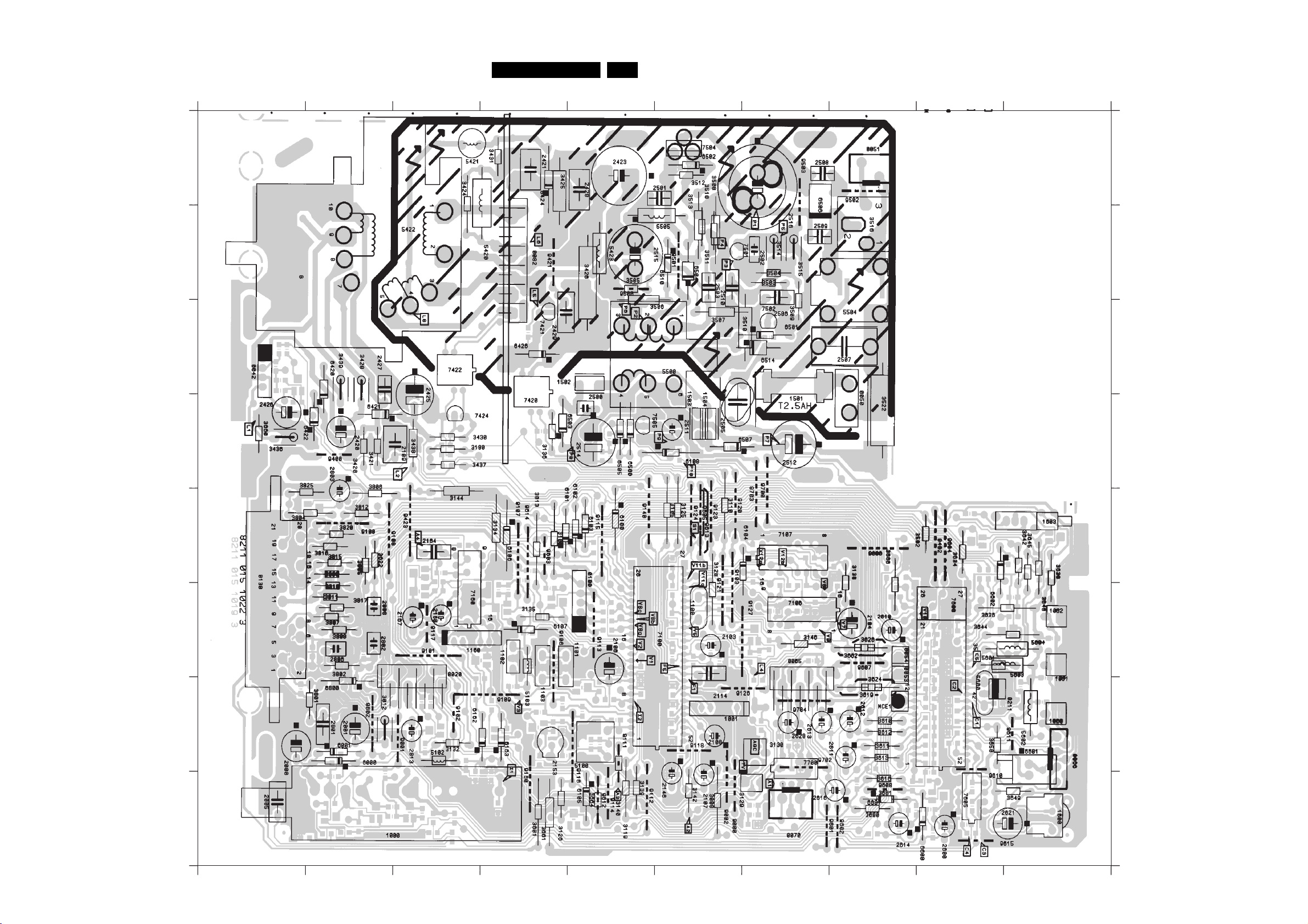
Diagram PWB
Power supply & Line stage (Diagram A1) 12 20,21
Tuner IF (Diagram A2) 13 20,21
Sound & Chroma (Diagram A3) 14 20,21
Controls & teletext (Diagram A4) 15 20,21
CRT panel (Diagram B) 16
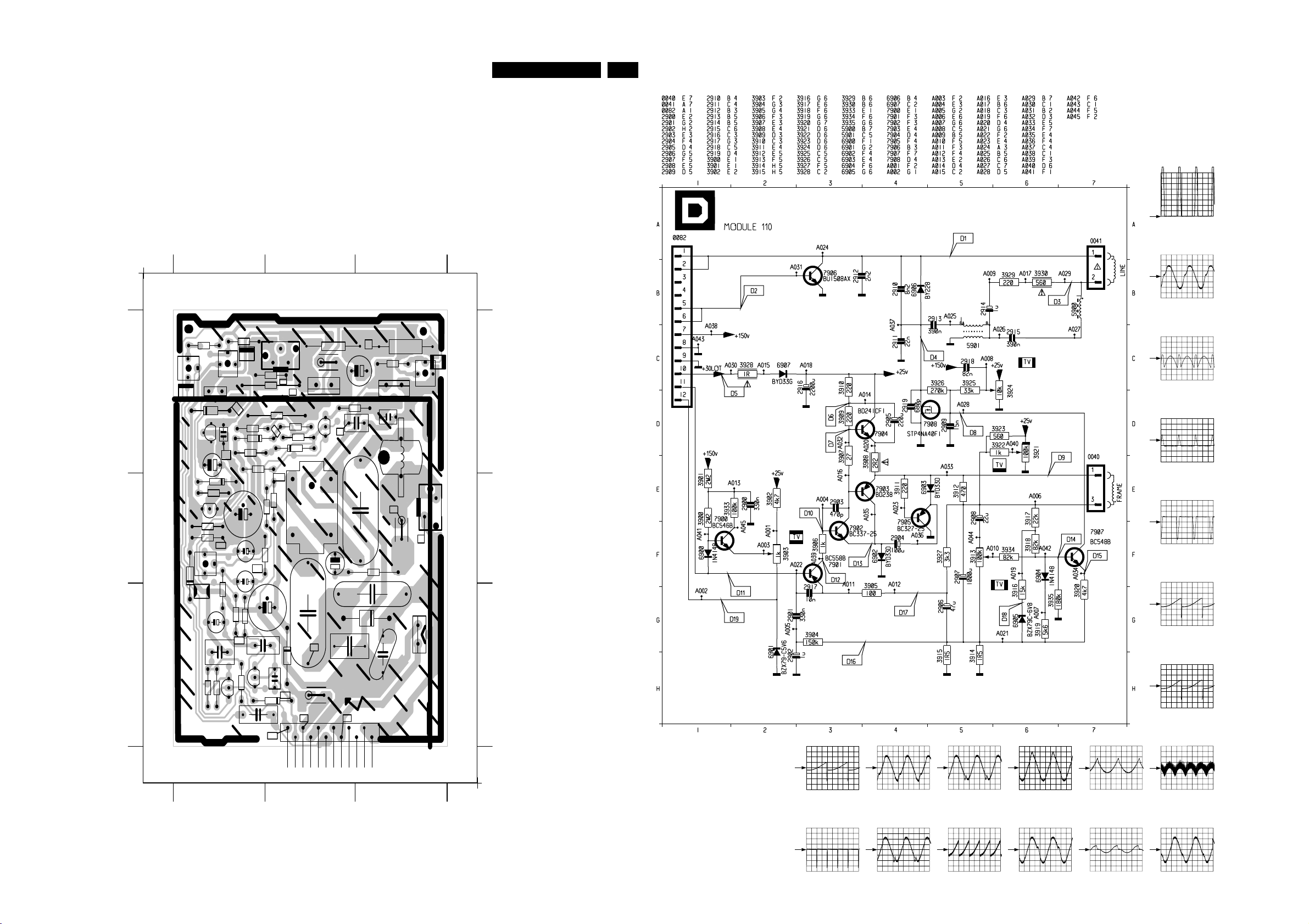
Deflection module 110 degrees (Diagram D) 17 17
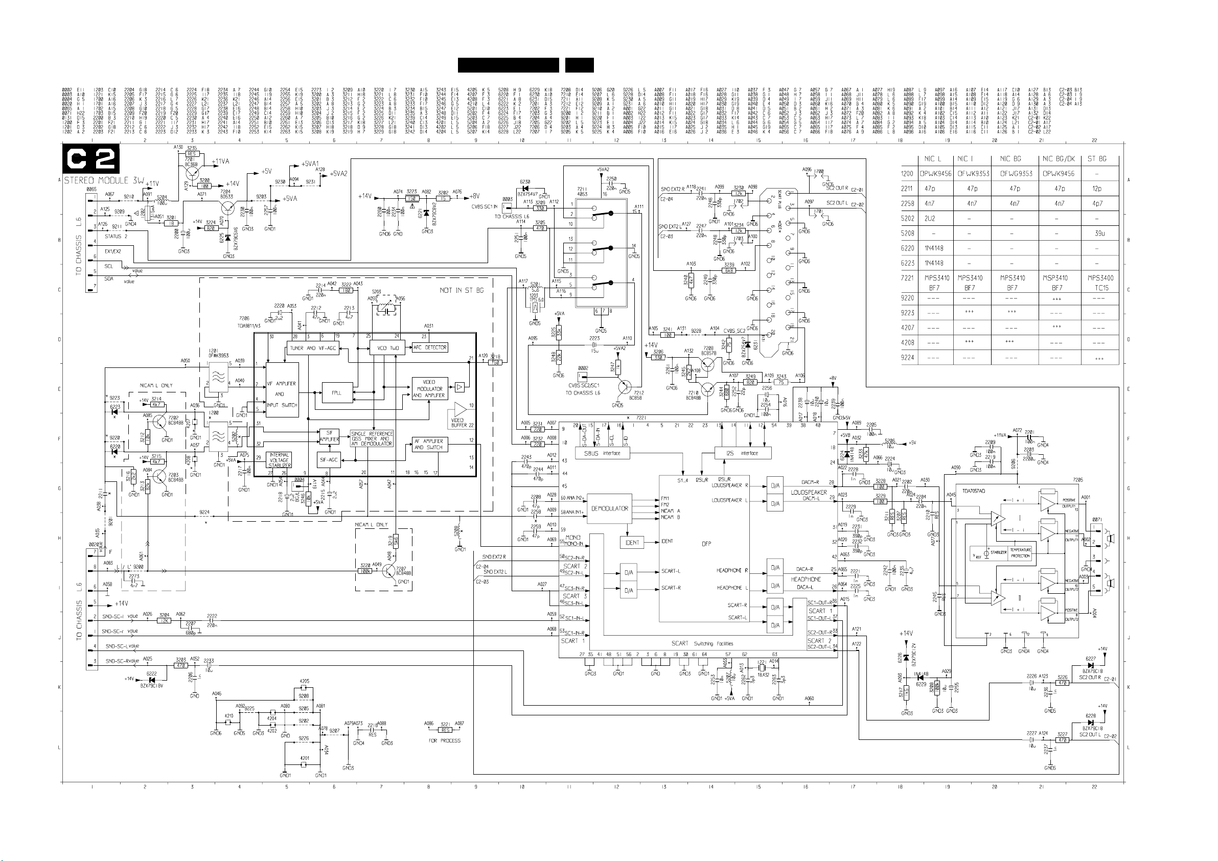
2 x 3W amplifier (Diagram C2) 19 18
Seperate controls & Mains module(Diagram J) 22
8 Electrical adjustments 23
9 Circuit Description 24
10 Directions for use/Exploded view cabinets 28, 35
11 List of abbreviations 36
Published by LV 9865 TV Service DepartmentPrinted in The NetherlandsCopyright reserved 1998 Philips Consumer Electronics B.V. Eindhoven, The Netherlands. All rights reserved. No part of this publication may be reproduced, stored in a retrieval system or transmitted, in any form or by any means, electronic, mechanical, photocopying, or otherwisewithout the prior permision of Philips.Subject to modification5 4822 727 21614
12 Spareparts list 38
Published by LV 9865 TV Service Department Printed in The Netherlands ©Copyright reserved 1998 Philips Consumer Electronics B.V. Eindhoven, The Netherlands. All rights reserved. No part of this publication may be reproduced, stored in a retrieval system or transmitted, in any form or by any means, electronic, mechanical,
Page 2
2 Comet
I
7
1 Technical specifications
Mains Voltage: : 220-240V ± 10% AC;
1 Technical specifications
50-60Hz (± 5%)
Mains frequency : 50 Hz
: 60 Hz
Power Consumption in stand-by : < 5 Watt
Power Consumption normal mode : 28” : 75Watt +/- 10%
Aerial input impedance TV : 75 Ohm - coax
Min. aerial input VHF: : 30mV
Min. aerial input UHF: : 40mV
Max. aerial input VHF/UHF: : 180mV
Pull-in range colour sync: : ± 300Hz
Pull-in range horizontal sync: : ± 600Hz
Pull-in range vertical sync: : ± 5Hz
Picture tube range : 25” and 28”
Sound output power : 3 Watt mono
execution
: 2 X 3 Watt stereo
execution
TV Systems: : PAL I
: PAL BG
: PALBG / SECAM DK
: PAL BG / SECAM LL'
Indications: : On Screen Display
(OSD) green/red
: 1 LED ( red high
intensity, red low
intensity,
: "RC5' and error
codes blinking red)
VCR programs: : 0
Tuning and operating system: : VST
UV913E / IEC (VST): : VHFa:46 - 102 MHz
: VHFb:138 - 224 MHz
: UHF:471 - 855 MHz
UV915E / IEC (VST): : VHFa:48 - 168 MHz
: VHFb:175 - 448 MHz
: UHF300 - 860 MHz
UV917E / IEC (VST): : VHFa:48 - 118 MHz
: VHFb:118 - 300 MHz
: UHF:470 - 861 MHz
U943 / IEC (VST): : UHF:470 - 861 MHz
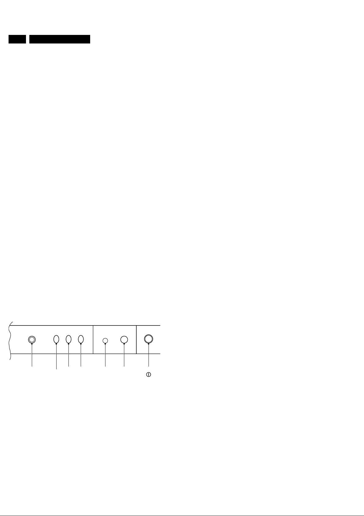
Local operating functions: : MENU / - / +
MENU
-+
IR LED,
76532029_002.A
03069
Page 3
2 Connection facilities
2 Connection facilities
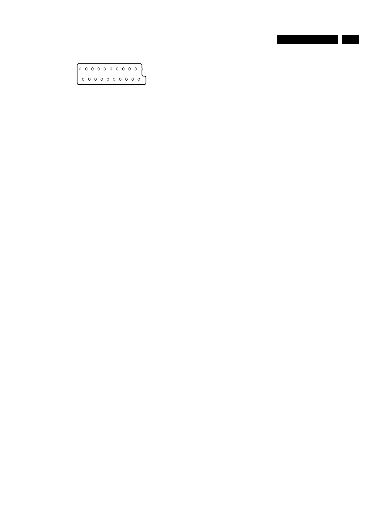
1- Audio R (0.5Vrms ≤1kΩ) k
2- Audio R (0.5Vrms ≥10kΩ) j
3- Audio L (0.5Vrms ≤1kΩ) k
4- Audio v
5- Blue v
6- Audio L (0.5Vrms ≥10kΩ) j
7- Blue (0.7Vpp/75Ω)
8- CVBS-
status 0-1.3V:INT, 4.5-7V:EXT 16:9, 9.5-
12V:EXT 4:3 j
9- Green v
1011- Green (0.7Vpp/75Ω)
1213- Red v
14- v
15- Red (0.7Vpp/75Ω)
16- RGB-
status (0-0.4V:INT, 1-3V:EXT/75Ω)
17- CVBS v
18- CVBS v
19- CVBS (1Vpp/75Ω) k
20- CVBS (1Vpp/75Ω) j
21- Earth
socket
3Comet
Page 4
4 Comet
3 Safety instructions, Maintenance instruction,
3 Safety instructions, Maintenance instruction, Warnings and Notes
3.1 Safety instructions for repairs
Figure 3-1
1. Safety regulations require that during a repair:
– the set should be connected to the mains via an
isolating transformer;
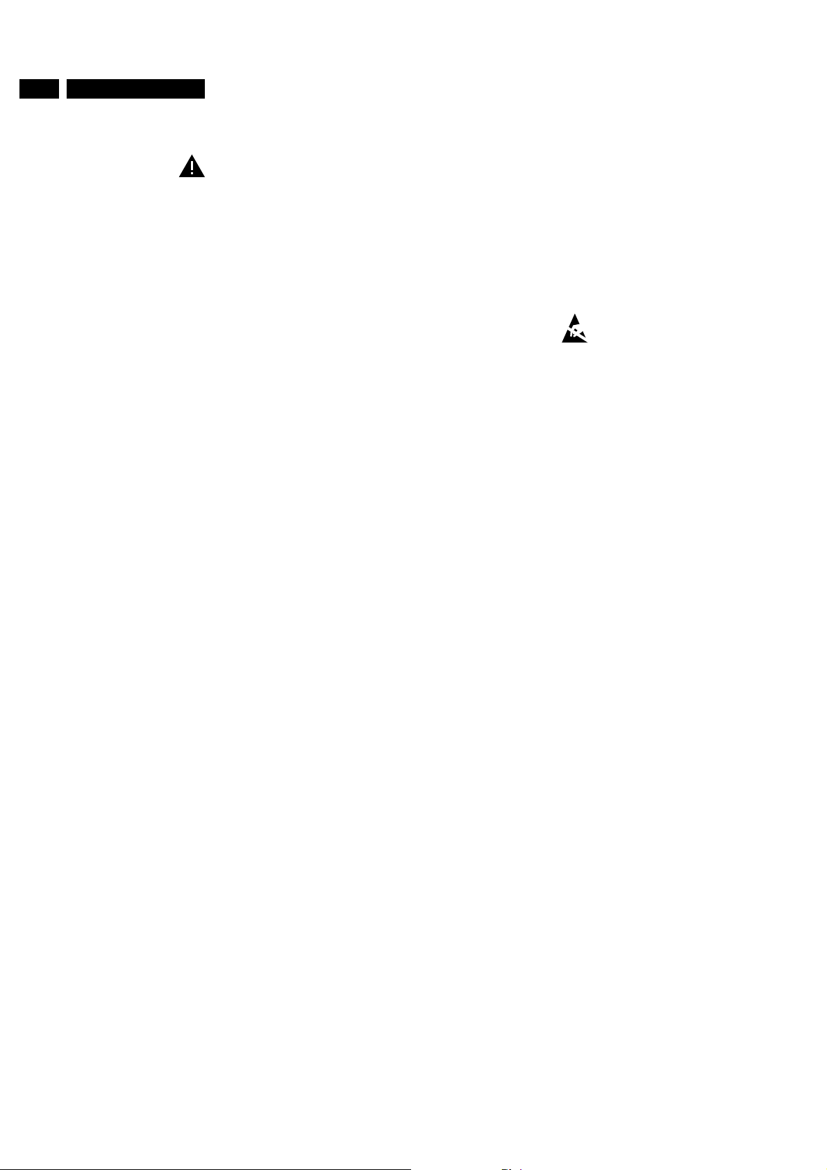
– safety components, indicated by the symbol (see fig.
3.1), should be replaced by components identical to
the original ones;
– when replacing the CRT, safety goggles must be worn.
2. Safety regulations require that after a repair the set must
be returned in its original condition. In particular attention
should be paid to the following points.
– As a strict precaution, we advise you to resolder the
solder joints through which the horizontal deflection
current is flowing, in particular:
• all pins of the line output transformer (LOT);
• fly-back capacitor(s);
• S-correction capacitor(s);
• line output transistor;
• pins of the connector with wires to the deflection
coil;
• other components through which the deflection
current flows.
Note: This resoldering is advised to prevent bad
connections due to metal fatigue in solder joints and is
therefore only necessary for television sets older than
2 years. The wire trees and EHT cable should be
routed correctly and fixed with the mounted cable
clamps.
– The insulation of the mains lead should be checked for
external damage.
– The mains lead strain relief should be checked for its
function in order to avoid touching the CRT, hot
components or heat sinks.
– The electrical DC resistance between the mains plug
and the secondary side should be checked (only for
sets which have a mains isolated power supply). This
check can be done as follows:
• unplug themainscordand connect a wire between
the two pins of the mains plug;
• set the mains switch to the on position (keep the
mains cord unplugged!);
• measure the resistance value between the pins of
the mains plug and the metal shielding of the tuner
or the aerial connection on the set. The reading
should be between 4.5 MW and 12 MW;
• switch off the TV and remove the wire between the
two pins of the mains plug.
– The cabinet should be checked for defects to avoid
touching of any inner parts by the customer.
– When the set is used in circumstances with higher dust,
grease or moisture levels, for example in a kitchen, the
recommended interval is 1 year.
– The maintenance inspection containsthefollowingactions:
• Execute the above mentioned 'general repair
instruction'.
• Clean the power supply and deflection circuitry on the
chassis.
• Clean thepicturetube panel andtheneck of the picture
tube.
3.3 Warnings
1. ESD
All ICs and many other semiconductors are susceptible to
electrostatic discharges (ESD). Careless handling during
repair can reduce life drastically. When repairing, make
sure that you are connected with the same potential as the
mass of the set by a wristband with resistance. Keep
components and tools also at this same potential.
– Available ESD protection equipment:
– anti-static table mat (large 1200x650x1.25mm) 4822
466 10953
– anti-static table mat (small 600x650x1.25mm) 4822
466 10958
– anti-static wristband 4822 395 10223
– connection box (3 press stud connections, 1 M ohm)
4822 320 11307
– extension cable (2 m, 2 M ohm; to connect wristband
to connection box) 4822 320 11305
– connecting cable (3 m, 2 M ohm; to connect table mat
to connection box) 4822 320 11306
– earth cable (1 M ohm; to connect any product to mat or
connection box) 4822 320 11308
– complete kit ESD3 (combining all 6 prior products -
small table mat) 4822 310 10671
– wristband tester 4822 344 13999
2. In order to prevent damage to ICs and transistors, all highvoltage flashovers must be avoided. In order to prevent
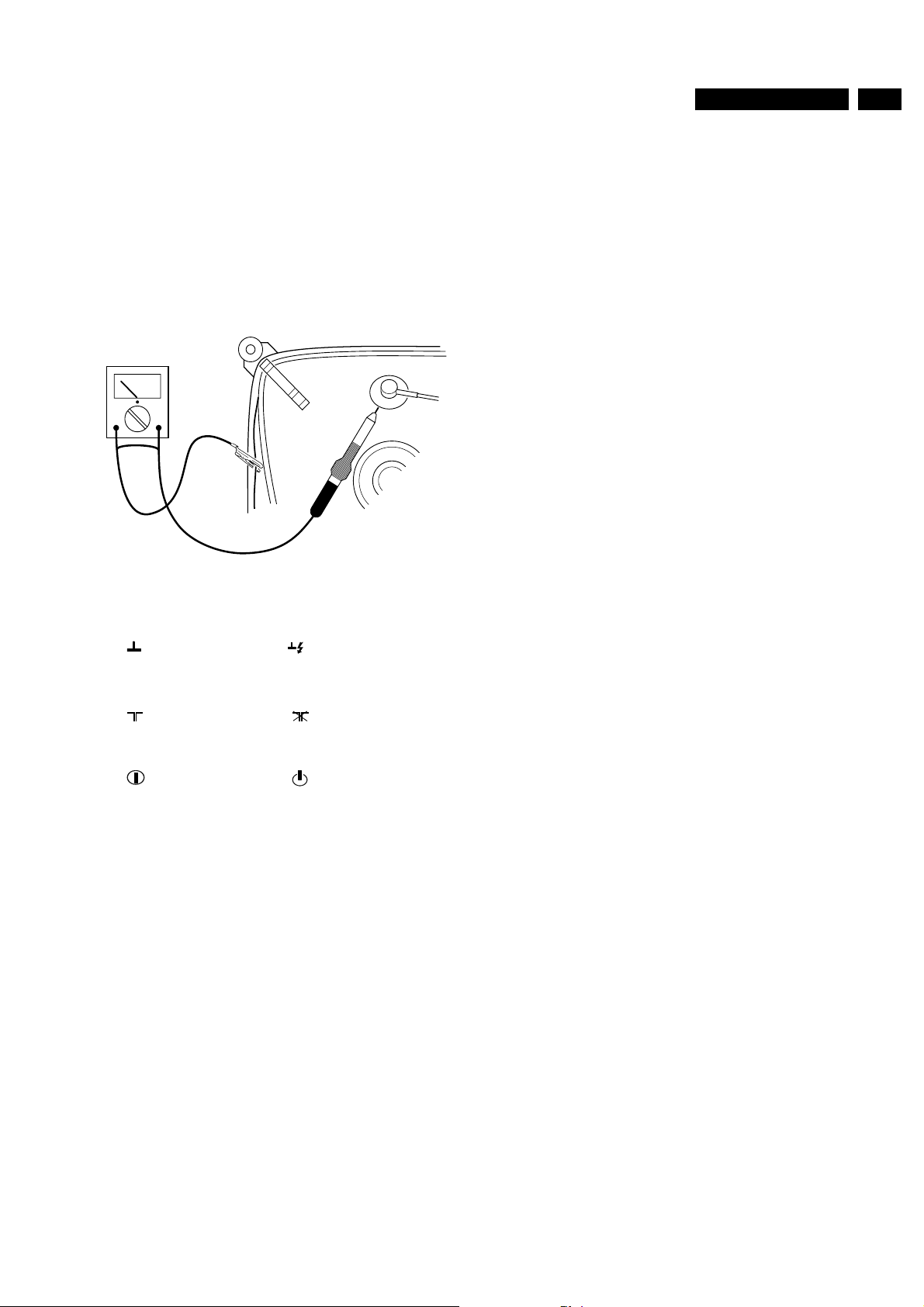
damage to the picture tube, the method shown in Fig. 3.2
should be used to discharge the picture tube. Use a highvoltageprobeandamultimeter(position DC-V). Discharge
until the meter reading is 0V (after approx. 30s).
3. Together withthedeflectionunit and any multipole unit, the
flat square picture tubes used from an integrated unit. The
deflection and the multipole units are set optimally at the
factory.Adjustmentof this unit duringrepairis therefore not
recommended.
4. Be careful during measurements in the high-voltage
section and on the picture tube.
5. Never replace modules or other components while the unit
is switched on.
6. When making settings, use plastic rather than metal tools.
This will prevent any short circuits and the danger of a
circuit becoming unstable.
7. Wear safetygogglesduringreplacementofthe picture tube
3.2 Maintenance instruction
It is recommended to have a maintenance inspection carried
out by a qualified service employee. The interval depends on
the usage conditions:
– When the set is used under normal circumstances, for
example in a living room, the recommended interval is 3 to
5 years.
3.4 Notes
1. The direct voltages and oscillograms should be measured
with regard to the tuner earth , or hot earth as this is called
(see fig. 3.3)
2. The direct voltages and oscillograms shown in the
diagrams are indicative and should be measured in the
Service Default Mode (see chapter 8) with a colour bar
signal and stereo sound (L:3 kHz, R:1 kHz unless stated
otherwise) and picture carrier at 475.25 MHz.
Page 5
3 Safety instructions, Maintenance instruction,
3. Where necessary,theoscillogramsanddirectvoltages are
measured with and without aerial signal. Voltages in the
power supply section are measured both for normal
operation and in standby . These values are indicated by
means of the appropriate symbols (see fig. 3.3).
4. The picture tube PWB has printed spark gaps. Each spark
gap is connected between an electrode of the picture tube
and the Aquadag coating.
5. The semiconductors indicated in the circuit diagram and in
the parts lists are completely interchangeable per position
with the semiconductors in the unit, irrespective of the type
indication on these semiconductors.
V
CL 26532098/042
140792
Figure 3-2
5Comet
tuner earth
tuner aarde
la masse du tuner
Tuner-Erde
massa del tuner
tierra del sintonizador
with aerial signal
met antenne signaal
avec signal d'antenne
mit Antennensignal
con segnale d'antenna
con la señal de antena
normal condition
normaal bedrijf
fonctionnement normal
normaler Betrieb
funzionamento normale
funcionamiento normal
massa calda
zonder antenne signaal
Figure 3-3
hot earth
hete aarde
la terre directe
heißen Erde
tierra caliente
without aerial signal
sans signal d'antenne
.ohne Antennensignal
senza segnale d'antenna
sin la señal de antena
stand by
stand by
position de veille
in Bereitschaft
modo di attesa
posición de espera
Page 6
6 Comet
4 Mechanical instructions
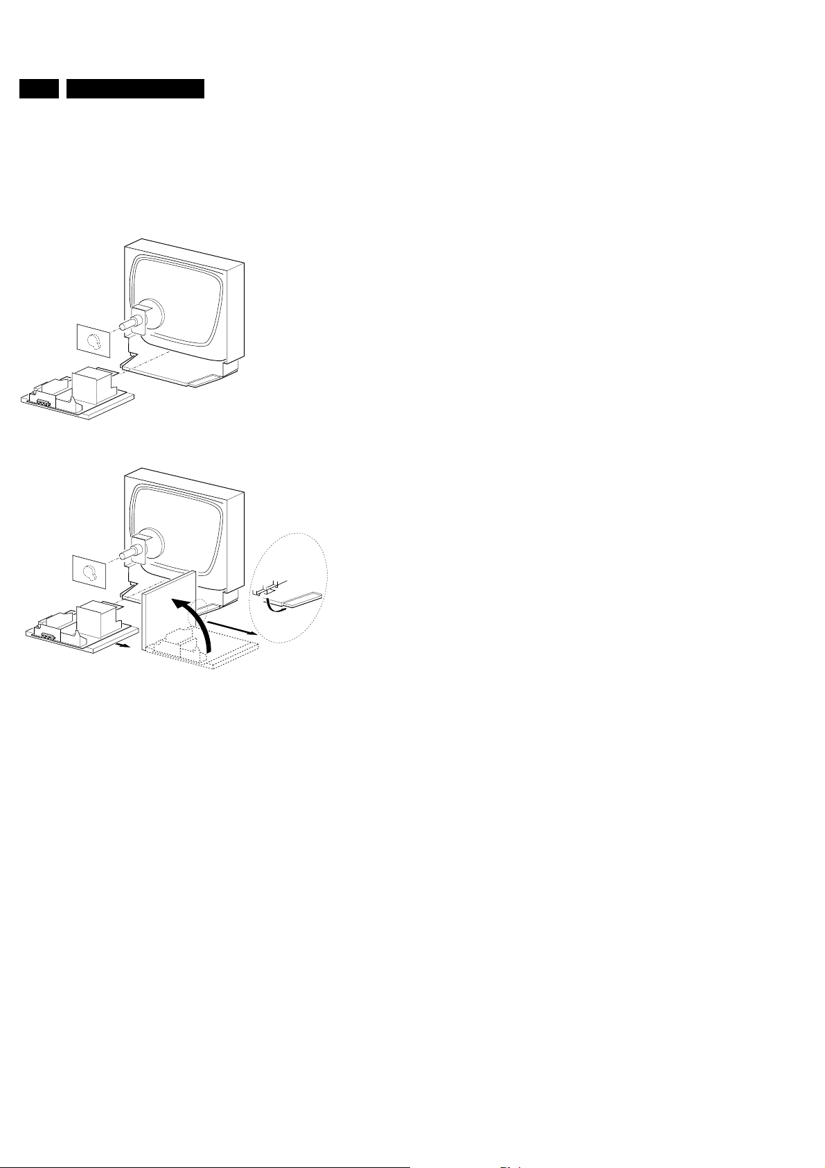
For the main carrier two service positions are possible:
4 Mechanical instructions
a. For faultfinding on the component side of the main carrier
b. For (de)soldering activities on the copper side of the main
carrier.
Position A can be reached by first removing the mains cord
fromit'sfixation, then loosenthecarrier lips and thenpullingthe
carrier panel for approximately 10 cm.
Position B can be reached from position A after disconnecting
the degaussing cable. A stable service position can be created
with the left hand side clip on the carrier panel and the cabinet
(see fig.4.1).
B
76532029_003
170697
Page 7
5 Repair facilities
7Comet
5 Repair facilities
5.1 Functional blocks
On both the service printing on the copper and the component
side, functional blocks are indicated by lines and text.
5.1.1 Test points
The L6 chassis is equipped with test points in the service
printing on both sides of mono-board. These test points are
referring to the functional blocks as mentioned above:
• P1-P2-P3, etc:Test points for the power supply
• L1-L2-L3, etc:Test points for the line drive and line output
circuitry
• F1-F2-F3, etc:Test points for the frame drive and frame
output circuitry
• S1-S2-S3, etc:Test points for the synchronisation circuitry
• V1-V2-V3, etc:Test points for the video processing circuitry
• A1-A2-A3, etc:Test points for the audio processing circuitry
• C1-C2-C3, etc:Test points for the control circuitry
• T1-T2-T3, etc:Test points for the teletext processing
circuitry
The numbering is done in a for diagnostics logical sequence;
always start diagnosing within a functional block, in the
sequence of the relevant test points, for that functional block.
5.1.2 Service default-alignment mode (SDAM)
Service default-alignment menu: new option settings are
activated immediately.
1. Software version of the microprocessor used in that typical
set is displayed in the right top corner
2. A counter in the middle of the screen indicate the normal
operation hours of the set in a hexadecimal code (every
time the set is switched "on" the counter is incremented by
1 hour, so +1 at the counter).
3. The "S" in the middle of the screen next to the counter
indicate that the set is in the service default-alignment
mode
4. Option codeThis code indicates the Options setting of the
set.
5. Error code history;
The 5 last different error codes occurred are stored in the
EEPROM memory; last error code detected will be displayed
on the left side (see for an overview of all possible error codes
Fig. 8.x), so e.g.:
0 0 0 0 0 means no error codes present in the buffer
30000meansoneerrorcode present in the buffer; error code
3
3 2 0 0 0 means two error codes present in the buffer; last
detected error code is error code 3, previous detected error
code is error code 2
The service default-alignment mode is a pre-defined mode
which can be used for faultfinding (especially when the TV
gives no picture at all). All oscillograms and DC voltages in this
service manual are measured in the service default-alignment
mode.
Activatingtheservicedefault-alignmentmodecanbe done in 2
ways:
1. By short-circuiting the service pins S1 and S2 of the
microcomputer (pin 14 of IC7600).
2. From normal operation mode by pressing the button
"DEFAULT" or "ALIGN" on the DST (Dealer Service Tool)
RC7150.
Leaving the service default-alignment mode to normal
operation can only be done by the stand-by on the remote
control or by pressing diagnose 99 followed by the OK-button
on the DST (so not via mains switch "off"; after mains switch
"off" and then "on" again the set will start up in the service
default-alignment mode again to enable easy faultfinding).
Functions of the service default-alignment mode:
1. All analogue settings (volume, contrast, brightness and
saturation) are in the mid position.
2. Set is tuned to program number 1
3. Delta volume settings are not used (delta volume setting =
a delta on the volume setting)
4. OSD error message (present available error code) is
displayed continuously
5. The OSD-key will act as search and auto store on the
maximum program number.
6. Automatic switch off function (set switches "off" after 15
minutes no IDENT) will be switched off
7. Hotel mode will be disabled
8. All other functions remain normal controllable
The errorcodehistorybufferisclearedwhenthe Service Menu
is left by the stand-by command or by diagnose 99 command.
In case the Service Menu is left by the mains switch "off" the
error code history buffer will not be cleared.
Optioncode +Counter +"S" for
service menu active +
software version->
Error code history --> 23000
Option setting row --> - SYSTE
Option setting:
In the bottom line the options are given.
Control of the options is with the following keys on the remote
control:
• PROGRAM +/-: Select the option to be changed; Via the
"PROGRAM +/-" button the option to be changed can be
selected.Theselectedoptionis implemented immediately.
• CONTROL up/down: Changes the setting of the option.
• MENU +/-: Changes toasubmenu;via"MENU +/-" buttons
a submenu is selected in which in a stereo version the
sound/sync alignment can be done.
The options are stored immediately in the EEPROM.
The following table indicates the possible hardware and
software options and their technical consequences:
001 0023S 1.0
M BG + I
+
Text displayed in the option row in the service menu The technical consequence for the selected option
SINGLE --> For a PAL BG only or PAL BG/SECAM BGDK set
Page 8
8 Comet
SYSTEM I:UK --> For a PAL I only set
SYSTEM BG+LL' -->For a PAL BG/SECAM LL' set
SYSTEM BG+DK --> For a PAL BGI/SECAM LL' set
NATIONAL BRAND MAxxxxx --> Selects MENU-Layout National Brand styling
5 Repair facilities
5.1.3 Error messages
The microcomputer also detects errors in circuits connected to
the I2C (Inter IC) bus. These error messages are
communicated via OSD (On Screen Display) and a flashing
LED in the service default-alignment mode. (error code history
buffer):
"OSD error number"
(servicemenu)
0 No blinking LED No error -1 LED blinks ones mC error IC7600
2 LED blinks twice General I2C error I2C bus is blocked
3 LED blinks three times EEPROM error IC7605
"LED behaviour" Error description Possible defective component
1. In normal operation; in normal operation no errors are
indicated.
2. In the service default-alignment mode; in the service
default-alignmentmode both the"OSDerror message"and
the "LED error" indication will display the present detected
error continuously.
Page 9

8 Electrical adjustments
8 Electrical adjustments
8.1 Adjustments on the 110 module panel
1. Horizontal amplitude: Is adjusted with potentiometer
R3924
2. Vertical centring: Is adjusted with potentiometer R3921
3. Picture height: Is adjusted with potentiometer R3903
4. East-west correction: Is adjusted by potentiometer R3913
5. Horizontal centring (main pcb):Is adjusted with
potentiometer R3129 on the main PCB
6. Focusing: Is adjusted with the focusing potentiometer in
the line output transformer
7. AFC
– Adjustment of the AFC and picture demodulator (all
versions).
– Select a non secam L/L' system in the SDAM mode
(negativemodulation).Switch the tuner toHIGHBAND
(pin 11 of tuner 1100 grounded). Connect a pattern
generator to pin17ofthetunerviaacapacitorof4.7nF
andputa82Wresistor from the output of the generator
toground.Connecta DC voltmeter to pin 44 ofIC7100.
Adjust coil 5100 to get 3V5 on pin 44 of IC7100.
– The signal of the generator has to be 38.9 MHz.
– Adjustment of the AFC and picture demodulator.
(BAND 1 L. France versions only).
– Same story as a) only the frequency of the generator
has to be 33.9Mhz with positive modulation.
23Comet
8. RF AGC
9. If the picture of a strong local transmitter is reproduced
distorted, adjust potentiometer R3130 until the picture is
undistorted.
or: Connectapatterngenerator(e.g.PM5518)to the aerial
input with RF signal amplitude = 1mV. Connect a
multimeter (DC) at pin 5 of the tuner. Adjust R3130 so that
voltage at pin 5 of the tuner is 8V5 +/- 0V5 DC.
8.2 Adjustments on the CRT panel
VG2 cut-off points of picture tube
Apply a black CVBS signal at the input pin 20 of scart. Adjust
thebrightnessin order to have 1.6V duringtheline at the R,G,B
outputs of the BIMOS pin 18,19,20 of IC7100. Put
potentiometers R3326, R3316 and R3306 to the minimum
value (maximum voltage on the CRT cathodes). Adjust now
VG2 till the colour that luminates first is not visible anymore.
Adjust now the other two potentiometers in such a way that
they just don't luminate.
Potentiometer R3308 should always be in the mid-position.
Page 10

24 Comet
9 CIRCUIT DESCRIPTION
9 CIRCUIT DESCRIPTION
9.1 Description of the power supply:
9.1.1 General
Note: The voltages +96S and +96s are not mains isolated.
Thepower-supplyused in this chassis is aself-oscillatingdown
converter with an auxiliary winding to help the FET to switch.
9.1.2 Principle of the down-converter (Fig 8.1):
WhenswitchTS7504 is closed,thevoltage on L2-3 isVin-Vout.
During this time, energy is stored in the coil and energy is
delivered to the load. When switch TS7504 opens, the energy
stored in the coil will be stored in the output capacitor (C2515).
This is due to the fact that the current through the coil has to
decrease linear. When the switch is open the current is floating
through D6504, L2-3 and C2515. By controlling the duty-cycle
of the switch, the output voltage can be regulated.
9.1.3 Start-up (see diagram A1):
When the switch TS7504 is closed, the input voltage is placed
over winding 2-3 of transformer 5500, which acts as coil L2-3
in Fig 8.1. Via resistors R3513,R3518 and R3512 the switch is
turned on for the first time. Zener diode D6502 prevents that
the Ugs of the FET becomes higher than 15V. When the input
voltage is on winding 2-3, there is also a voltage on winding 1-
2. Via winding 1-2 the correct switching voltage is obtained.
The DC-part of this voltage is blocked by capacitor C2503.
DiodeD6510actsasa protection in start-up and in short-circuit
situations.Duringstart-up the outputcapacitorC2515 is empty.
It takes a relative long time to charge the gate to a voltage high
enough to switch on the FET. This is due to the fact the diode
D6510 is conducting. When this diode is conducting, the
currentthatwould normally flow into the gateofthefet to switch
on the FET, is now flowing into C2515. In this way a smooth
start-up is guaranteed.
9.1.4 General way of working (Fig 8.2):
The state of the power-supply can be divided into three areas:
– T-on;In this state the FET is conducting and energy is
stored in the coil and in the output capacitor.
– T-off;In this state the fet is non conducting and the energy
stored in the coil is fed to the output capacitor.
– T-dead;Fet is out of conduction and there is no energy in
the coil.
T-on; In the T-on state, switch TS7540 is switched on. When
the switch is on the voltage over resistors R3514-R3515 is a
direct measure for the current through winding 2-3. This is a
negative voltage. When this voltage becomes below a certain
level, TS7501 starts conducting and will switch off the fet. In
this way it is prevented that the coil can go into saturation. This
could be the case when the output voltage is very low. (long on
time of the FET). When the output-voltage becomes too high
during T-on the FET will be switched off. (see Output-voltage
regulation)
T-off; Due to the stored energy a current will start to flow
throughD6504,C2515 and winding 2-3. Duetothefact that the
current is flowing through this circuit, a voltage with reverse
polarity is on winding 1-2. In this way the fet remains off until
thecurrentthroughwinding2-3 reaches zero. Now a new cycle
will start. The fet will be switched on and all starts over again.
T-dead; If the output voltage is too high (for example in a low
load situation) the FET remains off till the output-voltage is not
to high anymore.
9.1.5 Output voltage regulation:
This is done by the circuit D6501, R3509, TS7502, R3505,
R3507, R3510. Transistor TS7502 can only conduct when the
voltage on the base is 0V7 lower than the voltage the voltage
on the emitter. This means that the voltage drop over resistors
R3505 and R3507 should be 5V6(zenerdiode) + 0V7(baseemitter). This is reached when the output voltage exceeds the
100V. Now transistor TS7502 starts conducting, which brings
transistor TS7501 in conduction. As a consequence the gate
voltage of the fet becomes very low and the fet stops
conducting. As long as the output voltage is too high the fet
stays out of conduction.
9.2 Protections:
9.2.1 Overvoltage protection:
A disadvantage of a down converter is that if the switch
becomes a short-circuit, the output voltage will increase to the
input voltage. This could damage circuits. In this power-supply
there is a protection to prevent this. If the output voltage
becomes higher than 130V, zenerdiode D6514 starts to
conduct.TheVin will be shortcircuited.This will blown themain
fuse 1501 and protect in this way all the other circuits.
9.2.2 Short-circuit and start-up protection:
The short-circuit protection works the same as the start-up
protection. If the output-voltage is very low in case of a start-up
orashort-circuit condition, The gate willbecharged very slowly
due to the fact that zenerdiode D6510 is conducting. So the
current is not only charging the gate but is also flowing into the
output capacitor. In this way it takes a few milliseconds to
switch on the fet. Diode D6510 takes also care that the fet
never remains in his power consuming (linear) area.
9.2.3 Undervoltage protection
Iftheoutputvoltage is very low, it also takes a largetimebefore
the current through winding 2-3 reaches zero. The power
supplied to the circuit is in this way very low and protects in this
way the circuit.
9.2.4 Other output voltages:
The output voltages +8S, +9S and +5S are made by winding 5-
6.Duringthetime that the fet TS7504 is notconducting,energy
is transformed to this winding (flyback principle) and the
voltages mentioned above are created. From the +9S, the +5S
voltage is derived. This voltage is stabilized by transistors
TS7505, TS7500 and zenerdiode D6500. D6500 is the
reference voltage and TS7505 is delivering the current. When
zenerdiode D6500 starts conducting, the voltage over resistor
R3502 becomes high and a POR signal is created.
9.3 Degaussing:
R3516 is a dual PTC (2 PTC's in one housing). After switching
"on" the set, the PTC is cold, so low ohmic. This makes the
degaussing current high. After degaussing the PTC is heated,
so high ohmic. This makes the degaussing current low. After
degaussing the PTC remains heated by the mains.
9.4 Line-circuit (Diagram A1):
The primary side of the line-circuit and the deflection coil are
connected to the hot earth. The driver-circuit contains an optocouplertocreate isolation between the low-signal partsandthe
Page 11

9 CIRCUIT DESCRIPTION
25Comet
mains. The optocoupler is driven by pin 37 of IC7100-6E via
transistorTS7103.When TS7103 isnotconducting,(the LED of
the optocoupler is also out of conduction) TS7421 is also not
conducting. In this way TS7422 will conduct and the 96V is
placed over winding 2-1 of the LOT. A voltage over winding 21 of the LOT will cause a voltage over the windings 8-10, 6-10
and 9-10. Now energy will be transformed from the primary to
the secondary-side and charge capacitors C2424 and C2425.
C2430 will be charged to the difference of the +40D and +14D
(=26V) when TS7422 is conducting. When TS7422 stops
conducting, the voltage of pin 8 of the LOT will become very
negative. This forces C2430 to be charged to 26V plus the
absolute value of pin 8. When TS7422 starts conducting again
the voltage of pin 8 of the LOT will increase and so the voltage
on the anode of D6422. In this way the 160V is created. This
means that during the off-time of TS7422, C2430 is charged
andduringthe on-time of TS7422, theenergyinC2430 is given
to C2426. When transistor TS7103 conducts, the LED of the
opto-coupler will be activated. This causes the transistor of the
opto-coupler to conduct, which drives TS7421 in conduction.
ThisbringsTS7422outofconduction.Due to this construction,
this circuit is protected against missing line-drive pulses. When
a line-drive pulse is missed, the line-transistor stays out of
conduction, due to the fact that the diode of the opto-coupler is
forced into conduction by TS7103. In this way nothing can be
damaged when there is no line-drive.
Winding 4-3 is an extra winding to help TS7422 to switch.
On the secondary-side of the LOT there is a circuit consisting
of TS7423, R3422, R3433, R3434, C2431 and C2432. This
circuit creates a pulse when TS7422 switches off. This pulse
indicatesthathorizontal flyback takes place. Thisinformationis
fed to IC7100-6E to blank the picture.
9.5 Stand-by:
Thestandbysignal from the mC is lowincaseof stand-by. Now
TS7103 is brought into conduction by R3100. As mentioned
before this will switch off the line-output stage completely.
9.6 Deflection :
9.6.1 Horizontal deflection:
The voltage over capacitor C2422 is the same as the voltage
over C2515 (96V). When TS7422 is conducting this voltage is
placed over the horizontal deflection coil. This causes a linear
increasing current through this coil. In this way deflection is
created. When TS7422 switches of flyback takes place and it
starts all over again. L5424 is used for linearity correction.
9.6.2 Vertical deflection:
Vertical deflection is based on a balance amplifier. Or TS7401
or TS7402 is conducting. This depends on the signal V-drive. If
V-drive is high TS7401 conducts and the voltage of C2401 is
placedoverthe deflection coil. Now thepictureis written. When
V-drive is low, TS7402 conducts and the +40V supply voltage
minusthevoltage over C2401 is placed over thedeflectioncoil.
Flyback takes now place. In this way deflection is generated.
R3407 is used to adjust the vertical shift. With this resistor the
level of the signal VFB is adjusted. R3402 and C2404 are used
to damp oscillation of the deflection coil with his parasitic
capacitance. The signal NIL from the mC is used to create a
non-interlaced mode. This is done by creating a small DC
current through the deflection coil.
9.7 110 degrees deflection module
For the 25" and 28" sets a 110 degrees module is needed for
East/West correction. This panel is allocated on the right hand
side of the mainboard (seen from the rear). East/west
correction in this module is based on the diode-modulator
principle; the current through the horizontal deflection coil is
modulated. As this is done by a parabolic-shaped voltage, E/W
distortion is corrected. This parabolic-shaped voltage is
derived from a saw-tooth-shaped voltage of the frame
deflection.
9.7.1 Frame (time base frame)
Because the raster part is fed by the primary side a galvanic
isolator must be applied between IC 7100 (= so called Bimos
ic) in the secondary side and the raster amplifier on primary
side. This is realised by opto coupler (7422); this opto coupler
will be switched and it will block the saw-tooth of the Bimos ic.
So we don't use the saw-tooth of the Bimos((pin 42) or the
feedback frame input(pin 41). The only information from the
Bimosic(=IC7100) is the flyback command(pin43).The output
of this pin is a pulse of 6 to 0 Volts during 1 mS with a period of
20mS. This signal blocks transistor 7424 and this causes
conduction of the opto coupler diode (7422). The internal
transistor also conduct and pins 11 and 12 (connector 00820)
of the 110 module will be short circuited.
9.7.2 Raster part
A saw-tooth must be created because we don't use it from the
Bimos ic(see annex 5). Via 150V C2901 will be charged via
R3901, R3900 and D6900; the function of D6901 is to
determine the lower part of the potential level. After 20mS a
signalcomingfromthe Bimos ic will short-circuit pins 11and12
of connector 0082 and C2901 will be discharged. It is a must to
have an amplitude on the screen independent of the 50Hz or
60Hz frequency of the mains; see circuit diagram annex 6. The
emitter voltage of T7900 can be adjusted with potentiometer
3903; this is the top Voltage of the saw-tooth. This is the circuit
for adjusting the vertical amplitude independent of the 50/60Hz
frequency. The saw-tooth will control T7901 and this transistor
controls the amplifier (= T7902, T7903 and T7904).D6902,
D6903, T7905 and C2904 determines the flyback. This flyback
pulse is negative and is created by an inverted polarity of
C2904.During the deflection T7905 is blocked and C2904
charges; during the flyback T7905 conducts and the flyback
pulse will be made.
9.7.3 East-West modulator
The parabola is taken on C2907; R3916 and D6905
determines the shape of the parabola and they corrects the
upper and lower parts. The parabola is fed via C2908 to
potentiometer 3913; this for adjusting the pin-cushion
correction. Via T7904 this signal goes to MosFet 7908; the Vgs
command has two functions by changing the Voltage of Vgs by
potentiometer 3924: pin-cushion correction and horizontal
amplitude adjustment.
Special components:
• D6904 + R3916: temperature compensation of Vbe
(T7904)
• R3935: trapezium correction
• C2909: to avoid external radiation
• C2918: to avoid "twisted or broken" lines
Page 12

26 Comet
9 CIRCUIT DESCRIPTION
9.7.4 Line timebase
The control voltage of pin 37 of the Bimos ic (=ic7100) is
derived via opto coupler pos 7420 to transistor T7421; then
send via C2428 and C2421 to pins 5 and6 of connector 0082;
this is the control of the base of T7906 (=BU1508AX). At the
flyback diode between collector and mass there are two parts
present to allow the East/west modulation. One part of this
modulator consists of D6906, T7908, C2910 and C2911. The
second part another diode is not visible in the circuit diagram
but it is present in the MosFet 7908.
On pins 1 and 2 of the module the primary side of the LOT is
connected. The LOT supplies the following voltages:
• 3-5 : 26 Volts after smoothing
• 10-8: 14 Volts
• 9 : 160 volts for video amplifiers.
9.8 BIMOS IC: PAL I Version
9.8.1 Introduction
The TDA 8361 is a single chip video and audio processor and
it incorporates a built in IF-detector, Luminance and
Chrominance separator, PAL/NTSC Chroma Decoder, RGB
processing, Horizontal and Vertical Oscillators, Sync
Separators and the FM Sound demodulation circuit.
9.8.2 Bimos Start Up
The Bimos device (Line Oscillator) starts up via pin 36,
however it will only start up when the voltage on this pin has
reached 5.6 Volts. At 5.6 Volts the output frequency will be
about 25kHz. The supply voltage at this pin (Pin 36) is
produced by the Switched Mode Power Supply and not by the
Line Out Put Stage. Once the supply voltage on Pin 10 has
(Line Output Stage) reached the 8-volt threshold the output
frequency will switch to 15.625 kHz. The voltage on this pin is
prevented from exeading 8 volts by zener diode 6106 (Page
10)
9.9 Vertical Synchronisation and Frame Amplifier
9.9.1 The Vertical Sync Separator
This functional block separates the Frame Synchronisation
pulses from the CVBS signal, once these pulses have been
separated the pulses are then used to synchronise the Frame
Oscillator.
9.9.2 Amplitude
The voltage on pin 42 of the BIMOS device determines the
amplitude of the frame sawtooth.
9.9.3 Frame Pre Amplifier
This internal amplifier increases the amplitude of the Frame
sawtooth, from here the frame sawtooth is available at pin 43.
9.9.4 BCI Input Pin
This Input is fed into the BIMOS device form the Tube Base
Board, It is used to provide frame correction for changes in the
EHT voltage. For example if the EHT decreases (more white)
the picture will get larger. This results in the BCI decreasing
and the picture size being automatically corrected by the
BIMOS.
9.9.5 The IF Demodulator
The IF bandpass characteristic is determined by SAW filter
1001. The IF signal is then fed from here into BIMOS pins 45
and 46. Pin 1 of the IC is used for the selection of positive or
negative video modulation. It is high for positive modulation
and low for negative.
9.9.6 AGC
Pin 47 is used for AGC (AGC is used to adjust the gain of the
Tuner so that over modulation is avoided).
9.8.3 Horizontal Sync Separator
Thisfunctionalblockseparatesthehorizontal sync pulses from
the CVBS and then locks the pulses to the free running
horizontal sawtooh generator. However both the vertical and
horizontal oscillators are also internally locked to the 4.43 MHz
Chroma reference Crystal item 1100.
• The Horizontal Oscillator Saw Tooth Generator The
sawtoothisconverted to a squarewaveformwith a variable
duty cycle. This square waveform is then fed to the Line O/
P stage via a Galvanic Isolator. The correct line time
constant is automatically determined, internally by the
BIMOS IC.
• Pin 38 This is pin has two purposes, these are.
1. The Sandcastle Pulse O/P
2. Horizontal Flyback Pulse Input
1. The Sandcastle Pulse has an output current of a few
micro amps; the amplitudes of the sandcastle pulse
components are: Burst 5V3; Line Blanking 3V and
Frame Blanking 2V.
2. TheHORFLYBACK input has a currentof100-300 uA.
The Horizontal flyback pulse input, allows the phase of
the flyback pulse to be compared internally with the
phase of the horizontal oscillator; if the phase is not
correct, the horizontal oscillators duty cycle will be
adjusted accordingly.
9.9.7 AGC Threshold Adjustment
Variable resistor R3130 which is connected to pin 49 adjusts
the AGC Threshold
9.9.8 Automatic Frequency Control/ Pin 44
The AFC control signal is available at pin 44 of the BIMOS
device. It is obtained from the internal IF reference signal.
C2100 is used to smooth the AFC voltage.
9.9.9 IDENT Signal/ Pin 4
The IDENT signal on pin 4 is "High" when horizontal sync is
detected in the video signal and low when no sync is detected.
The IDENT line is connected to the main Microprocessor.
(Pin15)
9.9.10 What does the IDENT line do ?
It is used for tuning control (for switching from fast to the slow
tuning mode) Pin 4 (BIMOS) is also used by the
microprocessor (Pin15) for "No Signal Standby" after 15
minutes. Used to provide a stable OSD - Time constant
switched by the BIMOS.
Page 13

9 CIRCUIT DESCRIPTION
27Comet
9.9.11 IF Source Select, Luminance And Chrominance Separation.
The Baseband Video signal (normal amplitude 2Vpp) at Pin 7
also contains the inercarrier sound signal, however the sound
signalhasto be filtered out before theVideosignal can be used
. Ceramic filter 1102 (6 MHz) is used for this purpose. After the
filter has removed the sound, the Video signal is then fed back
into the IC at Pin13. From here the signal is internally fed to a
source selector switch, Pin16is used for source select control.
If Pin 16= 0V This is Internal Video Input Mode If Pin 16= 8V
External Video Input Mode Is Selected BIMOS Pin 16 is
controlled via the STATUS and the External 2 switching
signals, which originate from the main microprocessor.
9.9.12 Luminance And Chrominance Separation
The Chrominance signal is filtered out by using a Notch Filter,
the Notch Filter provides -20db of attenuation. The Notch Filter
is accurately internally calibrated by the subcarrier frequency
(4.43 MHz).
9.9.13 Sharpness Control-Pin 14
Picture Sharpness is adjusted at Pin 14 of the BIMOS IC. The
voltage variation expected here will be between 2.5V-5V.
Picture Sharpness is adjusted in the on screen Picture Menu.
9.9.14 Crominance Decoder
9.10.2 Fast Blanking
Via the FAST BLANKING signal available at pin 21 RGB input
selection is also made.
9.10.3 OSD FAST BL
Originates from the OSD generator; this signal is "high" (>1V)
to insert OSD characters.
9.10.4 F.BL.SCART
This is the fast blanking signal form pin 16 of Scart 1. This
signal is "high" (>1V) to switch the RGB source select into
external input mode.
Note: Scart 2 does not have RGB capability.
9.10.5 F.BL. TXT
FastBlankingsignal from the Teletext Decoder. This pinishigh
(>1V) to switch the RGB source select into external mode. Pin
22 Red, 23 Green and 24 Blue.
The Chrominance signal originating from the CVBS signal (Pin
7) is filtered and then applied back into the BIMOS via either
pins13or15.Pin16
is connected to the Microprocessor (Pin17 ) and is used for
internal/external video switching. The internal Chroma
Decoder is then internally fed with this selected feed, see page
11. From here the Chroma is fed to a pre amplifier and then on
to the Burst Demodulator, the next stage is the R-Y and B-Y
Demodulator. The Line and Frame Oscillators also use the
4.43 MHz reference signal available at pin 35.
9.9.15 Pin 27
IsusedforChroma standards selection, however as these sets
are PAL only this pin is permanently forced in the PAL system
via this pin. To facilitate this 5.5 Volts is applied to this pin via
R3104 and R3145, 4K7.
9.9.16 Pin 32
This pin is used in combination with a separate SECAM
decoder, it is used to select either the PAL or SECAM colour
systems.
For PAL only sets, this pin will be set at 1V5 volts.
9.10 Video Controller Section: RGB-Dematrixing
This block dematrixes the -(R-Y), -(B-Y) and the Y signals into
RGBsignals;the Sandcastlepulse, which isderivedinternally,
synchronises the internal RGB dematrixing process, it is also
used to suppresses the RGB output signals during Frame
Flyback.
9.10.1 Analogue Control
– 0-4V5 /Contrast Pin 25
– 0-5V /Brightness Pin 17
– 0-2V5 /Saturation Pin 26
Page 14
28 Comet
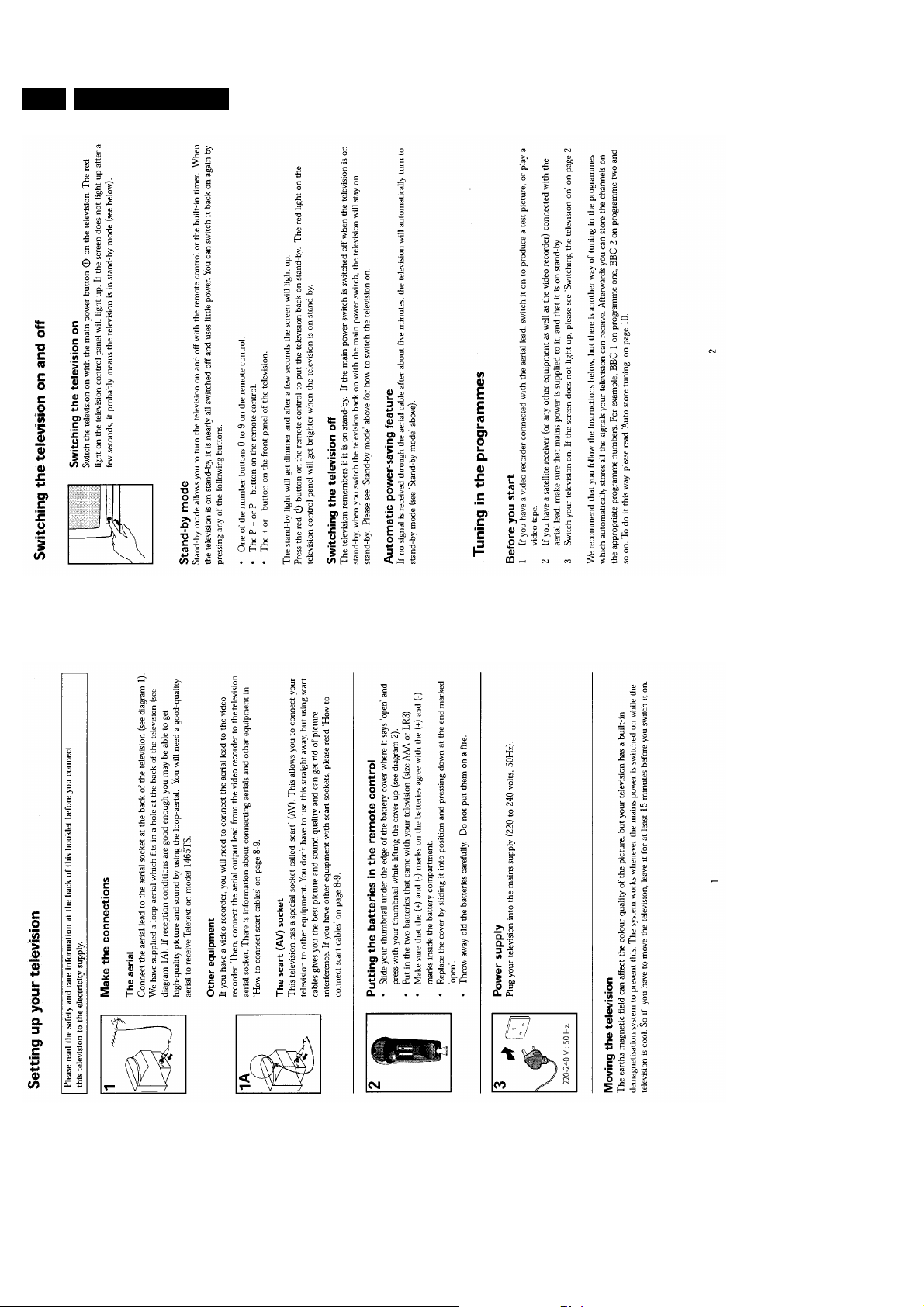
10 Direction for use
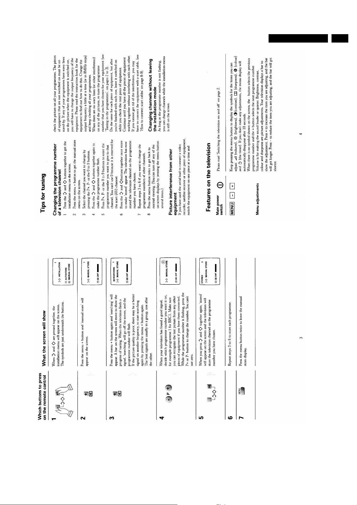
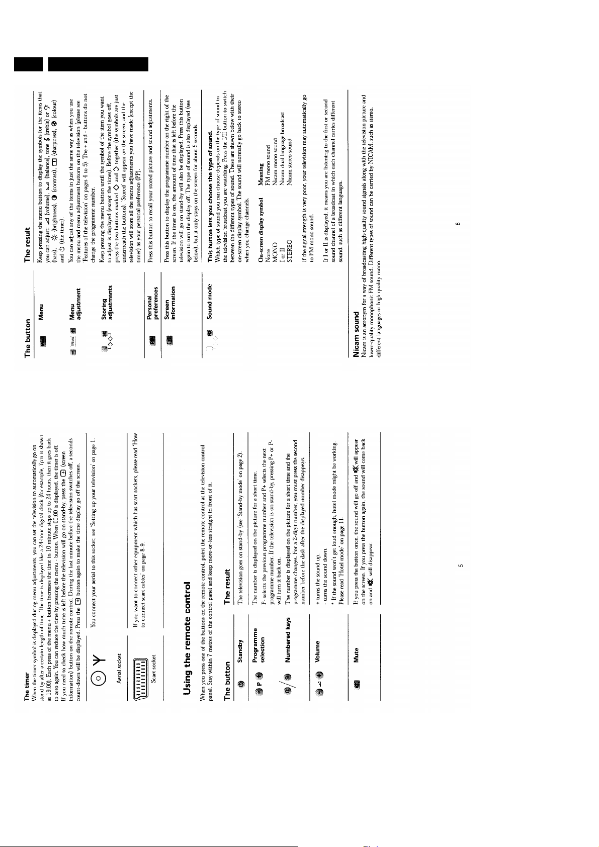
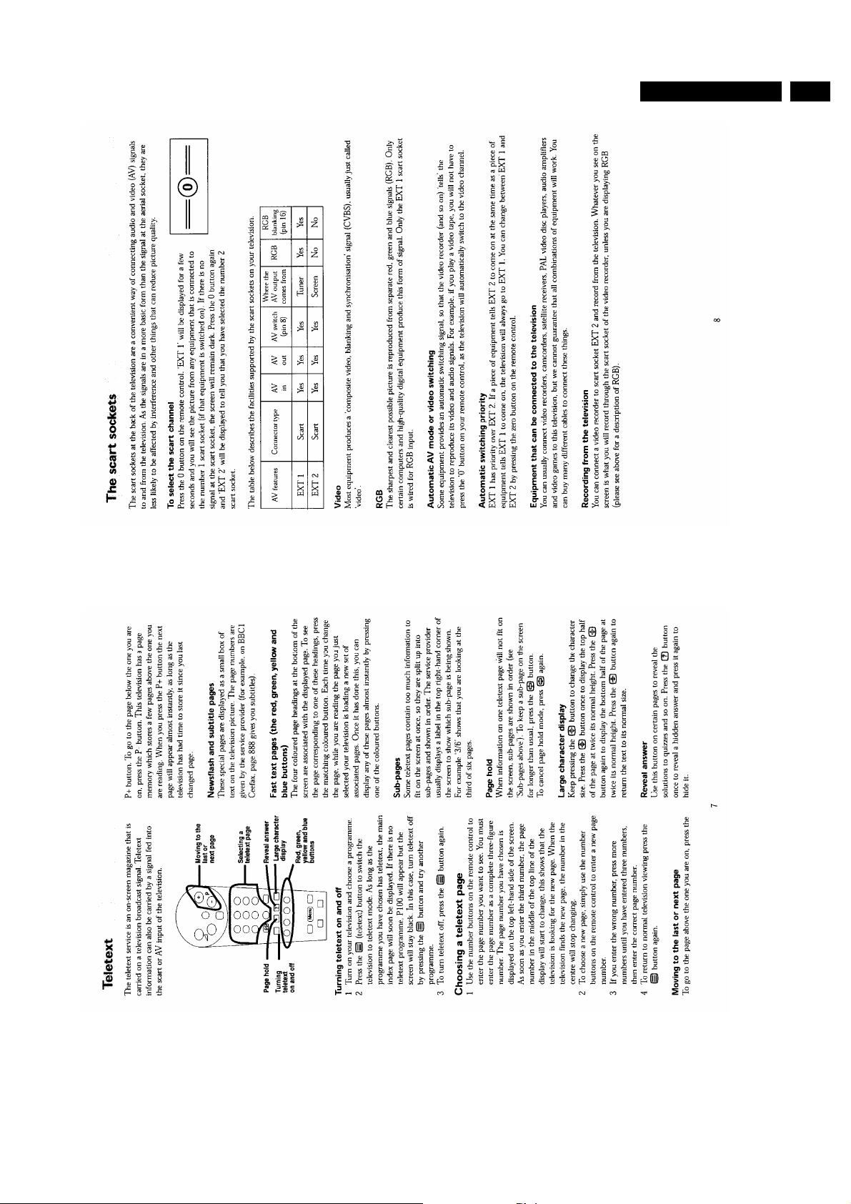
10 Direction for use
Page 15
10 Direction for use
29Comet
Page 16
30 Comet
10 Direction for use
Page 17
10 Direction for use
31Comet
Page 18
32 Comet
10 Direction for use
Page 19
10 Direction for use
33Comet
Page 20
34 Comet
10 Direction for use
Page 21
10 Direction for use
35Comet
6
5
4
1
8
7
9
10
11
12
290698
com_119.eps
2
3
8
9
10
12
13
11
2
1
3
16
151417
19
18
20
5
6
4
22
21
7
23
290698
com_129.eps
Page 22

36 Comet
11 List of Abbreviations
+96S Supply voltage from the SMPS to the line
output stage.This voltage is 104V for 21" sets.
+160V Supply voltage from the LOT for the CRT-
panel.
+40D Supply voltage from the LOT for vertical
deflection.
+8V Supply voltage for AM-sound.
+8Vx +8V Supply voltage from the SMPS for the
whole small signal part. x can be (a,b,c,d).
+5Sx +5V supply voltage from the SMPS to the µC
and periphery. x can be (a,b,c,d).
mC Microcomputer.
AFC Automatic Frequency Control.
AGC Automatic Gain Control.
AQUA Aquadag on the rear side of the picture tube to
pin 8 of the LOT.
ATS Automatic Table Setting (auto install system
for Germany only).
AUDIO-OUT Outgoing audio signal from pin 15 IC7140 to
pin 1 and 3 from scart.
B-SC-IN Blue input signal from the scart to the video
controller IC7015-6D.
BASEBAND CVBSBaseband CVBS signal from the IF-
detector IC7015-6B to the FM-demodulator
IC7015-6F.
BEAM INFO Beam Current Info; If beam current increases
the BCI signal decreases. BCI is used for
contrast reduction (if beam current is too high)
and picture correction (if beam current
increases (more white), EHT decreases so
picturewill become toobig,BCI decreases and
the picture will be corrected).
BRIGHTNESS Controlsignal(from µC, butonDC level viaRC
network) for brightness control of the video
controller IC7015-6D (0-5V).
BS1 Switching signal from the µC to select tuner-
band.
BS2 Switching signal from the µC to select tuner-
band.
C Chrominance part of the video signal; this
signal is also directly input at the SVHS plug.
CCT Computer Controlled Teletext.
CONTRAST Control signal (fromµC, but on DClevelvia RC
network) for contrast control of the video
controller IC7015-6D (0-4V5).
CVBS Colour Video Blanking Synchronisation
(present behind soundtrap 1102).
CVBS-SC-IN Incoming CVBS signal from pin 20 of scart to
the external input pin 15 IC7015-6B.
EEPROM Electrical Erasable Programmable Read Only
Memory.
ESD Electrical Static Discharge.
FBL Fast blanking signal made by adding the fast
blanking signals of the µC and the SCART fast
blanking signals.
FBL-SCART Fast blanking input signal from scart which is
added to the other fast blanking signals to
control the video controller IC7015-6D.
FBL-µP Fast blanking signal from the µP which is
added to the other fast blanking signals to
control the video controller IC7015-6D.
ff Filament (heater voltage) from LOT to the
picture tube.
FLOF Full Level One Feature.
FM FM demodulated sound from the FM-
demodulator IC7015-6F.
G-SC-IN Green input signal from the scart to the video
controller IC7015-6D.
H.DRIVE Horizontal drive signal from IC7015-6E to line
output stage.
HFB Horizontal flyback pulse (15625 Hz) used for
locking the horizontal oscillator in IC7015-6E.
I2C Digital control bus of the microcomputer.
11 List of Abbreviations
IDENT Status signal from IC7015-6B; "low" for no
CVBS signal (horizontal sync not present),
"high" in case CVBS signal is present
(horizontal sync present) from the IF-detector
IC7015-6B to the µC.
IF Intermediate frequency signalfromthe tuner to
the AM-demodulator IC7125.
LF-input Low frequency sound-signal. Input signal for
sound amplifier.
L/BG Switching signal from µC; "low" for LL
reception (positive modulation, AM sound),
"high" for BGIDK reception (negative
modulation, FM sound). The µC makes BG/L
"high" in case EUROPE or UK is selected, and
"low" in case FRANCE is selected.
L/L' or BGDK Incase of a LL' set, selection is made between
L and L'. In case of a BGDK set, selection is
made between BG and DK. If this pin is "high"
then L' or DK is selected.
NIL Non Inter Lace; 25 Hz block-shaped signal
from the_µC to the frame amplifier for
coinciding the odd & even frames.
OSD-B Blue info from OSD generator in µC to the
video controller IC7015-6D for inserting blue
info on the screen.
OSD-G Green info from OSD generator in µC to the
video controller IC7015-6D for inserting green
info on the screen.
OSD-R Red info from OSD generator in µC to the
video controller IC7015-6D for inserting red
info on the screen.
POR Power On Reset; ensures the µC starts up its
software only if the power supply of the µC
itself is high enough.
PP Personal Preference.
R-SC-IN Red input signal from the scart to the video
controller IC7015-6D.
RAM Random Access Memory.
ROM Read Only Memory.
SANDCASTLE Sandcastlesignal from IC7015-6Ftodelay line
IC7271 and SECAM chroma decoder IC7250.
SANDCASTLE1 Sandcastle signal from IC7015-6F to µC.
SATURATION Control signal (fromµC,but on DClevelvia RC
network) for saturation control of the video
controller IC7015-6D (0-2V5).
SAW Surface Acoustic Wave; high precision
bandpass filter.
SCL Clock line of the I2C-bus.
SDA Data line of the I2C-bus.
SDAM Service Default-Alignment Mode; predefined
mode for faultfinding (see chapter 8).
SHARPNESS Control signal on DC level (0-5V) from µC to
IF-detector IC7015-6B) for sharpness control.
SM Service Menu.
SMPS Switched Mode Power Supply.
SND-SC-l Incomming audio signal from pin 6 from the
scart. This signal is the left audio-channel.
SND-SC-r Incoming audio signal from pin 2 and pin 6
from scart. In case of a stereo set this is the
scart-input for the right sound channel.
SND-SC-L Outgoing audio signal from pin 3 to the scart.
This signal is the left audio-channel.
SND-SC-R Outgoing audio signal from pin 1 and pin 3 to
scart. In case of a stereo set this is the scart-
output for the right sound channel.
STANDBY/AFC Switching signal from µC; "low" for standby
(power supply will be switched to stand-by
mode), "high" for normal operation. This pin
acts also as an input for AFC.
STATUS Switching signal; "low" for internal CVBS,
"high" for external CVBS.
TOP Table Of Pages.
Page 23

11 List of Abbreviations
mP INT/EXT Switching signal from the µC for internal or
external audio + video switching ("low" for
external and "high" for internal).
VDRIVE Vertical drive signal from IC7015-6E to frame
amplifier.
V-vari Tuning voltage from µC to the tuner (0-30V
DC).
VFB 50 Hz vertical flyback pulse used for locking
the vertical oscillator in IC7015-6E.
VFL Signal to inform the µC that vertical flyback
takes place.
Vg2 Voltage on grid 2 of the picture tube.
VIP Video Input Processor.
VOLUME-L Controlsignal(from µC, butonDC level viaRC
network) for volume control in mono BG-sets.
VOL-LEVEL Controlsignal(from µC, butonDC level viaRC
network) for volume control in mono multi-
france sets.
WST World System Teletext.
Y Luminance part of the video signal; this signal
is also directly input at the SVHS plug.
37Comet
Page 24
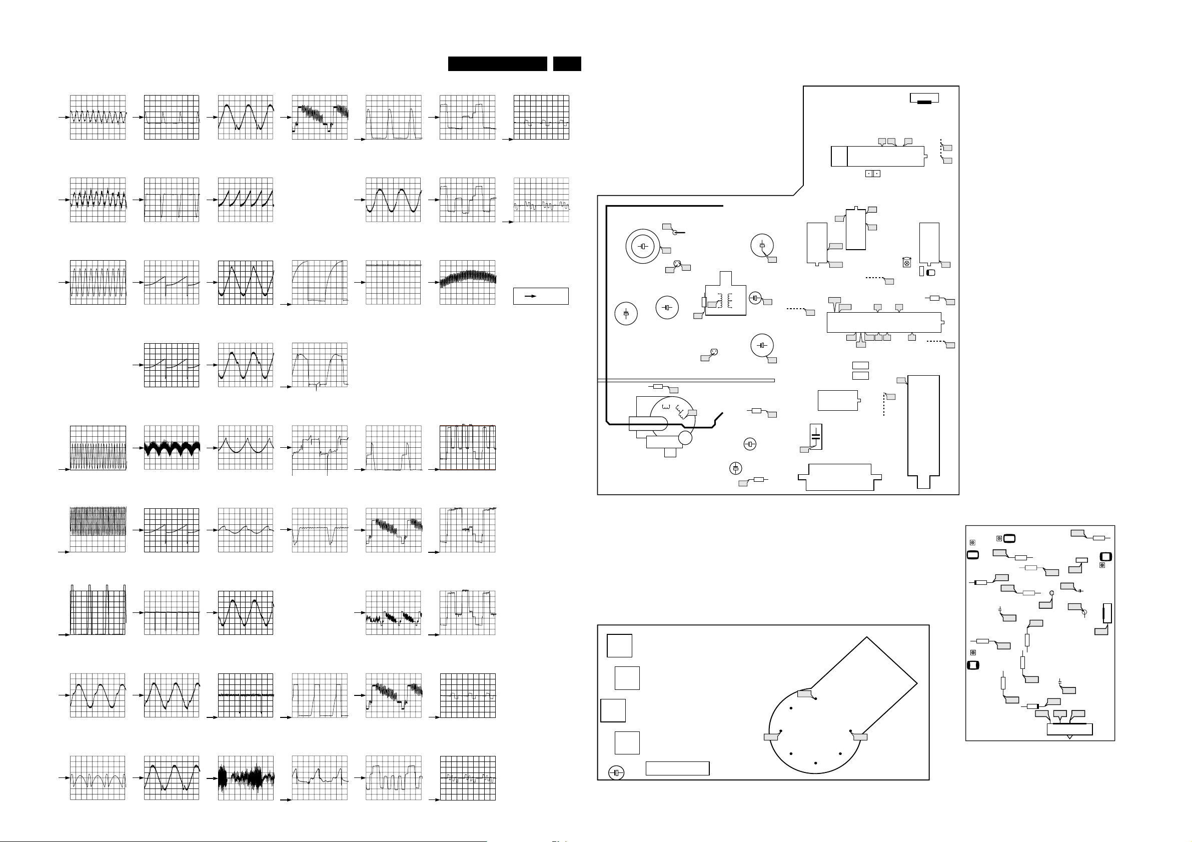
6 Overview oscillograms
9Comet
6 Overview oscillograms
A1
50mV / div AC
1ms / div
A2
20mV / div AC
1m s / div
A3
100mV / div AC
1ms / div
A4 Not present
C1 5V DC
C3 5V DC
C4 5V DC
C2
D4
5V / div AC
20µs / div
D5
5V / div AC
20µs / div
D6
1V / div AC
5ms / div
D7
1V / div AC
5ms / div
D8
D13
0.5V / div AC
10µs / div
D14
50mV / div AC
10ms / div
D15
2V / div AC
5ms / div
D16
2V / div AC
5ms / div
D17
I2
500mV / div AC
10µs / div
L1 140.3V DC
L2 13.6V DC
L4
500mV / div DC
10µs / div
L5
1V / div DC
10µs / div
L6
P4
50V / div DC
5µs / div
P5
2V / div DC
5ms / div
P6
2V / div DC
5ms / div
P7 10.3V DC
P8 10.2V DC
P9 5.4V DC
S1
V4b
10V / div AC
10µs / div
V4c
10V / div AC
10µs / div
V5
20mV / div AC
1µs / div
V6 Secam
(Only)
V7 Secam (Only)
V9 8V6 DC
V8a
V12a
0.5V / div DC
20µs / div
V12b
0.5V / div DC
20µs / div
= 0V
2423
2516
2515
3424
12
LOT
P5
3514
P1
7501
eb
c
P4
L6
0066
7100
719
I2
52
128
7700
3129
TUNER
TV
3142
9111
9615
116141
1131820
C3
C4
A1
A2
A3
C1C5
0054
1
3
8
0053
V7
V9
9127
TDA 8361
15
V2
9109
C2
4327 38
42
AGC
3130
L4
F1V5
43352928
V1
I1
V3
7600
21
7106
7107
2512
2511
3438
P7
P9
2514
P8
L2
P3
5500
1
6
2
P2
7421
5
4
3
c
3506
P6
L5
3
4
L8
5
8
9124
S1
7160
2164
16
V6
V12b
V12a
V11b
V11a
V8c V8a
V8b
1101
1103
16
9
8
1
1V / div DC
0.5µs / div
C5
500mV / div DC
0.5µs / div
D1
10V / div DC
20µs / div
D2
2V / div AC
5ms / div
D3
20mV / div AC
10ms / div
D9
1V / div AC
5ms / div
D10
0,5V / div AC
10ms / div
D11
2V / div AC
5ms / div
D12
0.2V / div AC
5ms / div
D18
0.2V / div AC
5ms / div
D19
2V / div AC
5ms / div
F1
2V / div DC
5ms / div
I1
500mV / div DC
10µs / div
L8
10V / div DC
10µs / div
P1 320V DC
P2
50V / div DC
5µs / div
P3
1V / div DC
10µs / div
V1
500mV / div AC
10µs / div
V2
2V / div DC
5ms / div
V3
500mV / div AC
10µs / div
V4a
500mV / div DC
10µs / div
V8b
500mV / div DC
10µs / div
V8c
500mV / div DC
10µs / div
V11a
1V / div DC
20µs/div
V11b
3326
3308
2330
3316
3306
8100
2426
2420
L1
3660
A4
V4b
G2
R
V4c V4a
G1
SCART
21 19 17 15 13 11 9 7 5 3 1
0130
G
B
F
F
1100
CL 76532029_006.AI
110697
3903
3923
D6
D4
5
D4
D3
GS
7908
2909
3930
3910
TV
D
3924
0043
D1
1
76532029_004.AI
170697
2
1
TV
3921
D9
TV
6902
3915
TV
2903
D13
D16
D18
D10
3906
D12
3912
3916
3927
3907
3935
D17
6900
D14
D19
0082
D15
D7
7907
2913
D11
12
D8
D5 D2
10
5V / div AC
2V / div AC
50mV / div DC
100mV / div DC
10V / div AC
1V / div DC
Verzamel.AI
CL 66532008_013.AI
150296
Page 25
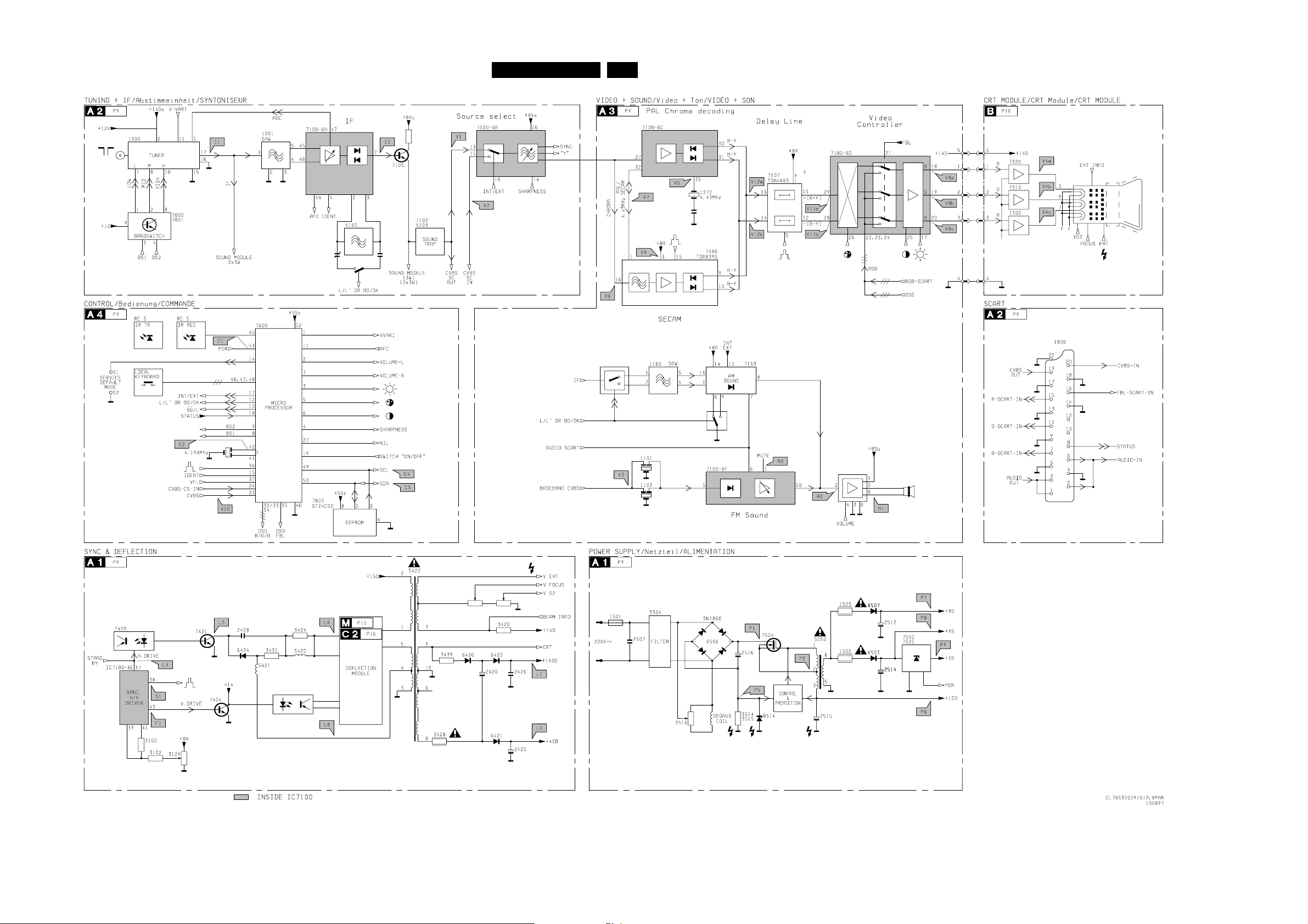
6 Overview oscillograms
10Comet
Page 26
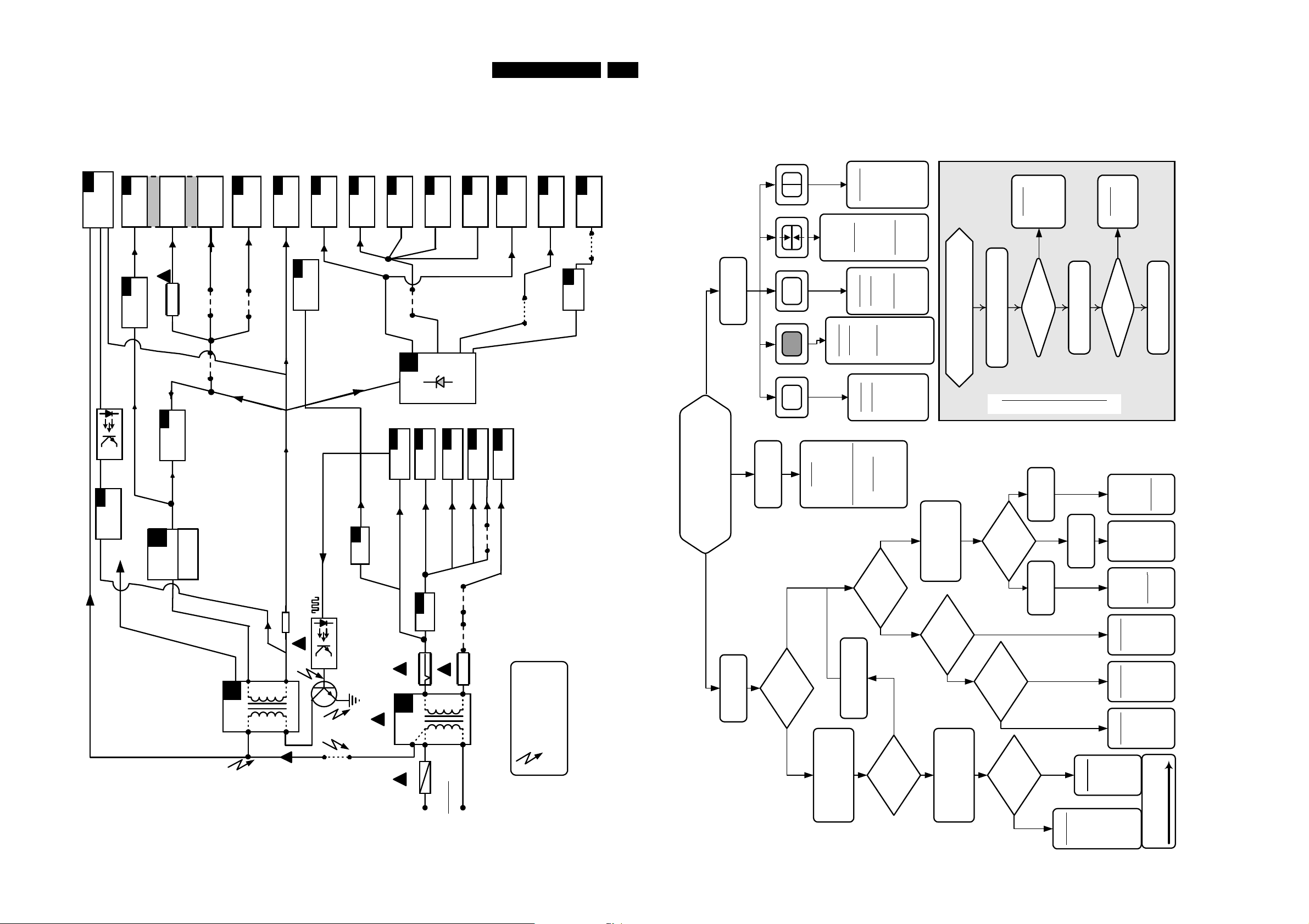
6 Overview oscillograms
11Comet
D
Deflec-
A1
150
A2
Tuner
tion Module
0 - 33v
A4
7422
Sync
7100-6e
THT
+25 KV
V- Vari
D6420
Band-
!
3012
+14D
B1
A1
D6422
switch
+12v
+14Da
Panel
CRT
+160D
C2426
Tuner
Pump
Band
+14Db
9001
9108
Charge
switch
A3
L/L'
Switch
+14Dc
9101
A1
LOT
B
or BG/DK
+14D
+14D
+14 Lot
A3
Beam Info
+8V
A4
P.O.R.
R3438
!
AM Sound
7420
7422
9420
A3
Delay
+8Va
POR
A1
TS
+150
7107
7500
!
A3
Det. 7106
Secam
+8Va
9616
+14D
Sync
Horz. Vert.A1IR-LED
+9s
!
A1
Power
!
A2
A4
+5Sa
+5S
A1
TS7505
1502
Supply
1101
A1
7100-6a
Sync
8Va
ON/OFF
Receiver
+5Sb
+9S
!
220v~
A2
7700-6a
IF-Det.
+8Va
D6107
A4
Func.Switc
hA4Control
+5Sa
+5Sc
9610
9700 9704
1503
+TXT
A2
"Y"+
Source sel.
+8V
A3
Audio
Sound 7700
+8Sb
A3
7100-6b
+8Vd
9617
!
TTENTION
A
AM/FM
Selection
+8Vd
"
ISOLATED
MAINS
OT
"N
A1
A1
7100-6e
SYNC
9124
T7423
8Vf
No
No Picture
Sound = OK
SET
THE
ON
WITCH
or Remote Control)
S
(with the mains switch
No Sound
Coulor
White
Picture = OK
YesNo
Is
No Sound
No Picture
=>150Vdc ?
Voltage +150
3928
Check:
T7903
T7902
Voltage:
Check:
on 110 PCB
Voltage:
Check:
Voltage:
Check:
Check
Pin1 Ic7700,
R3523 (3,3ohm)
Voltage: +8Sb on
Signal on:
+14D, VG2
+8Va, Ic7107
Check
Voltage:
Signal on:
Pin4 Ic7700,
Controlvoltage on
Signal on
Reconnect L5423
measure +150 again
Disconnect L5423 and
coil
Line
deflection
Plug 0041
D5
P43
IC7100
Signal on:
Plug 0040
+8A,
Signal on:
p36 Ic7600
p35 Ic7100
p5 Ic7100
P21 Ic7100
+150V
T7906,
P30 Ic7100
P31 Ic7100
P7 Ic7100
-Ic7100
IC7700
Pin6 Ic7100,
Pin50 Ic7100,
Yes
= OK ?
pin 1of LOT
No
Yes
=>150Vdc ?
Voltage +150a
Check:
mainstransformer.
D6906
Connect TV set to a variable
Switch "ON"
Service-default
alignment mode
= OK ?
Signal "L4"
Yes
No
Measure voltage
Connect scoop to Ts7504
Adjust mains-voltage to 40V~
LED
Blinks "N" times
No
= OK ?
Signal "L5"
Yes
Is
"P1" on C2516
=>300Vdc?
Voltage C2516
D6502,
Ts7502
Ts7501,
No
Yes
is switching?
The FET 7504
Increase mains-voltage
Blinks
"Three times"
Blinks
Blinks
"One time"
No
Yes
D6501,
Ts7502
Check:
Yes
No
Voltage on
to 82 - 85V~
C2515 >100Vdc?
"SOPS" supply is OK!
"First check after repair"
Error
Eeprom
"Two times"
Check:
Check:
Check:
D6510
D6502,
Ts7504
Check:
IC7605
Check:
C BUS
2
blocked
Error or
I
:
Ic 7600
Check
µp Error
D6503
Ic7100
Supp.+9S
Fuse 1502
Ts7421
Ts7103,
Ts7420,
D6424
No
Fuse
1501,
D6506,
Check:
R3514,
D6514,
Ts7504
R3515
If replace def. comp. do,
"First check after repair"
Page 27
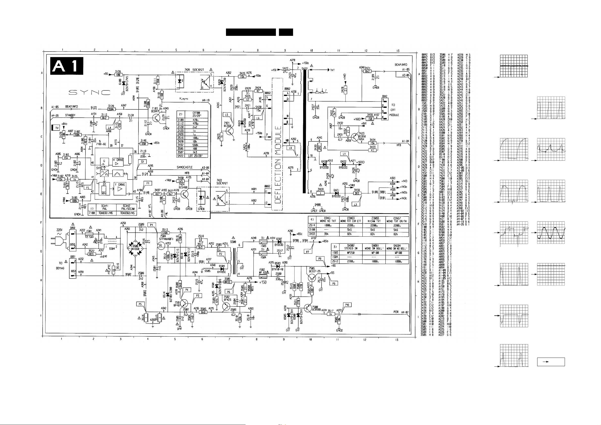
7 Electrical diagrams and print lay-outs
7 Electrical diagrams and print lay-outs
12Comet
F1
2V / div DC
5ms / div
L1 140.3V DC
L2 13.6V DC
L3 39V DC
L4
500mV / div DC
10µs / div
L5
P1 320V DC
P2
50V / div DC
5µs / div
P3
100mV / div DC
5µs / div
P4
1V / div DC
10µs / div
L6
500mV / div DC
10µs / div
L7
100V / div DC
10µs / div
L8
10V / div DC
10µs / div
S1
50V / div DC
5µs / div
P5
2V / div DC
5ms / div
P6
2V / div DC
5ms / div
P7 10.3V DC
P8 10.2V DC
P9 5.4V DC
1V / div DC
10µs / div
= 0V
OSC_A1.AI
Page 28
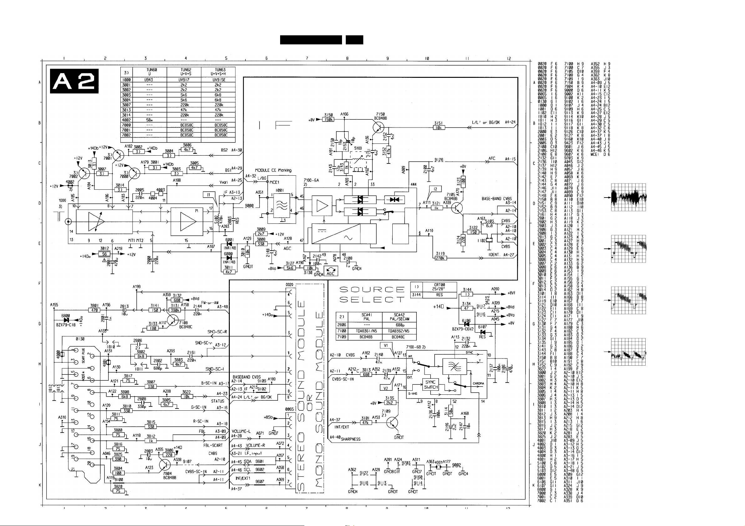
7 Electrical diagrams and print lay-outs
13Comet
I1
50mV / div DC
10µs / div
I2
500mV / div AC
10µs / div
V1
500mV / div AC
10µs / div
V2
2V / div DC
5ms / div
OSC_A2.AI
Page 29
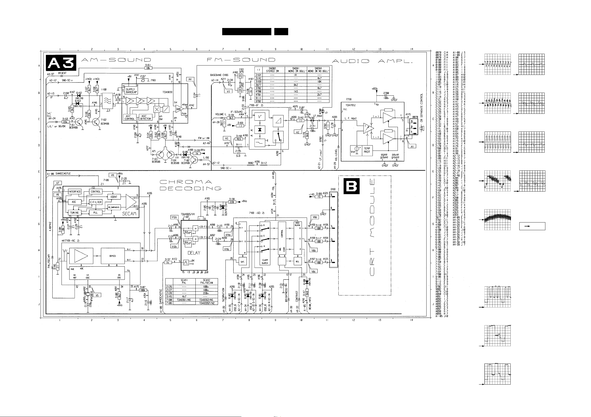
7 Electrical diagrams and print lay-outs
14Comet
A1
50mV / div AC
1ms / div
A2
20mV / div AC
1ms / div
A3
100mV / div AC
1ms / div
V3
500mV / div AC
10µs / div
V5
V11a
1V / div DC
20µs / div
V11b
1V / div DC
20µs / div
V12a
0.5V / div DC
20µs / div
V12b
0.5V / div DC
20µs / div
20mV / div AC
1µs / div
V7 Secam
V9 8V6 DC
V8a
500mV / div DC
10µs / div
V8b
500mV / div DC
10µs / div
V8c
(Only)
= 0V
500mV / div DC
10µs / div
OSC_A3.AI
Page 30
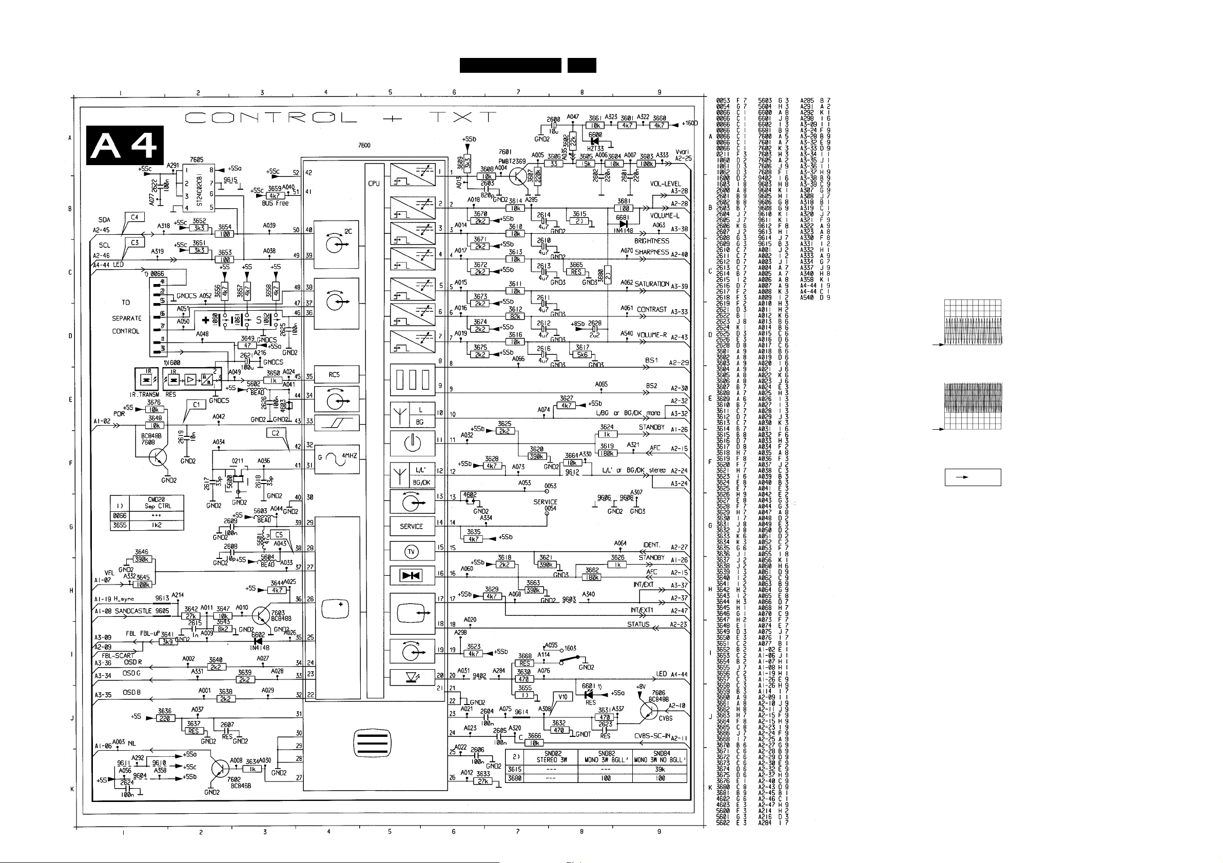
7 Electrical diagrams and print lay-outs
15Comet
C1 5V DC
C3 5V DC
C4 5V DC
C2
1V / div DC
0.5µs / div
C5
500mV / div DC
0.5µs / div
= 0V
OSC_A4.AI
Page 31
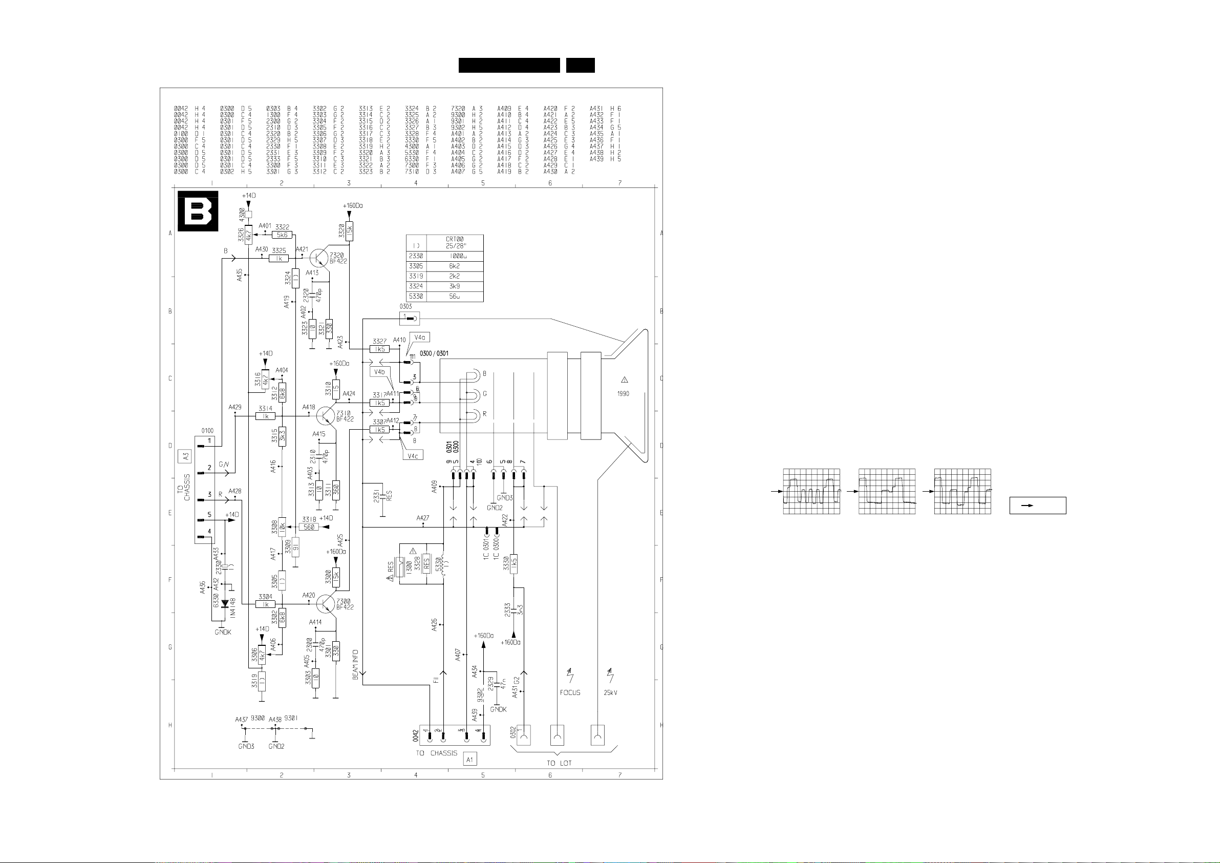
7 Electrical diagrams and print lay-outs
16Comet
V4a
10V / div AC
10µs / div
V4b
10V / div AC
10µs / div
V4c
= 0V
10V / div AC
10µs / div
OSC_B.AI
Page 32
7 Electrical diagrams and print lay-outs
0040 A 2
2904 A 3
2911 C 2
2918 C 2
3905 C 3
3912 A 3
3919 A 2
3926 A 1
0041 B 1
0082 C 1
2900 C 3
2901 C 3
2902 C 3
2903 A 3
2905 A 1
2906 B 3
2907 B 3
2908 B 3
2909 A 1
2910 C 1
2912 C 1
2913 C 2
2914 B 2
2915 B 1
2916 C 2
2917 C 2
2919 A 1
3900 C 3
3901 C 3
3902 A 3
3903 A 3
3904 B 3
3906 C 3
3907 A 2
3908 A 2
3909 A 1
3910 A 1
3911 B 3
3913 B 3
3914 B 3
3915 B 3
3916 A 2
3917 A 3
3918 A 2
3920 A 2
3921 A 3
3922 A 3
3923 A 2
3924 A 1
3925 A 1
3927 B 3
3928 C 2
3929 B 1
3930 B 1
3933 C 3
3934 B 2
3935 B 2
5900 B 1
5901 B 2
6900 C 3
6901 B 3
6902 A 3
6903 B 3
123
A
B
C
3902
1
3903
23
TV
E
6902
B
7902
2904
6903
AK
7905
3914
3915
AK
6901
TV
8211 015 1023 3
3922
3921
1
23
7903
B
C
D
AK
13
D13
C
2903
E
AK
D10
3911
EBC
2907
D16
2908
1
3913
2906
23
3904
3906
2902
D12
2900
C
B
E
3900
7900
3933
TV
3917
6905
3919
D12
3901
3912
3920
D17
3905
B
A
2918
3923
3927
2916
2901
C
E
0040
2
3
3907
3934
7901
6900
D19
3908
1
7904
B
D9
C
3916
D
18
3918
AK
6904
D14
3935
1
6907
AK
2917
D11
K
12
11
7907
3
5901
2913
D4
3928
0082
D5
3909
C
E
4
2
2914
D6
2905
E
3926
B
D8
2909
2915
6906
AK
2911
D2
GS
2919
3929
2910
2912
2
1
3925
7908
D3
D
3910
6904 A 2
6905 A 3
6906 C 2
6907 C 2
7900 C 3
7901 C 3
7902 A 3
1
3924
5900
0041
1
3930
D1
E
7906
B
7903 A 3
7904 A 2
7905 B 3
7906 C 1
7907 A 2
7908 A 1
TV
23
2
C
A
B
C
17Comet
D1
10V / div DC
20µs / div
D2
2V / div AC
5ms / div
D3
5V / div AC
20µs / div
D4
5V / div AC
20µs / div
D5
5V / div AC
20µs / div
D6
1V / div AC
5ms / div
D7
D9
D11
D13
D15
D17
d.eps
130697
1V / div AC
5ms / div
D8
1V / div AC
123
5ms / div
D10
0,5V / div AC
10ms / div
2V / div AC
5ms / div
D12
2V / div AC
5ms / div
0.5V / div AC
10µs / div
D14
50mV / div AC
10ms / div
2V / div AC
5ms / div
D16
2V / div AC
5ms / div
0.2V / div AC
5ms / div
D18
0.2V / div AC
5ms / div
20mV / div AC
10ms / div
D19
2V / div AC
5ms / div
Page 33
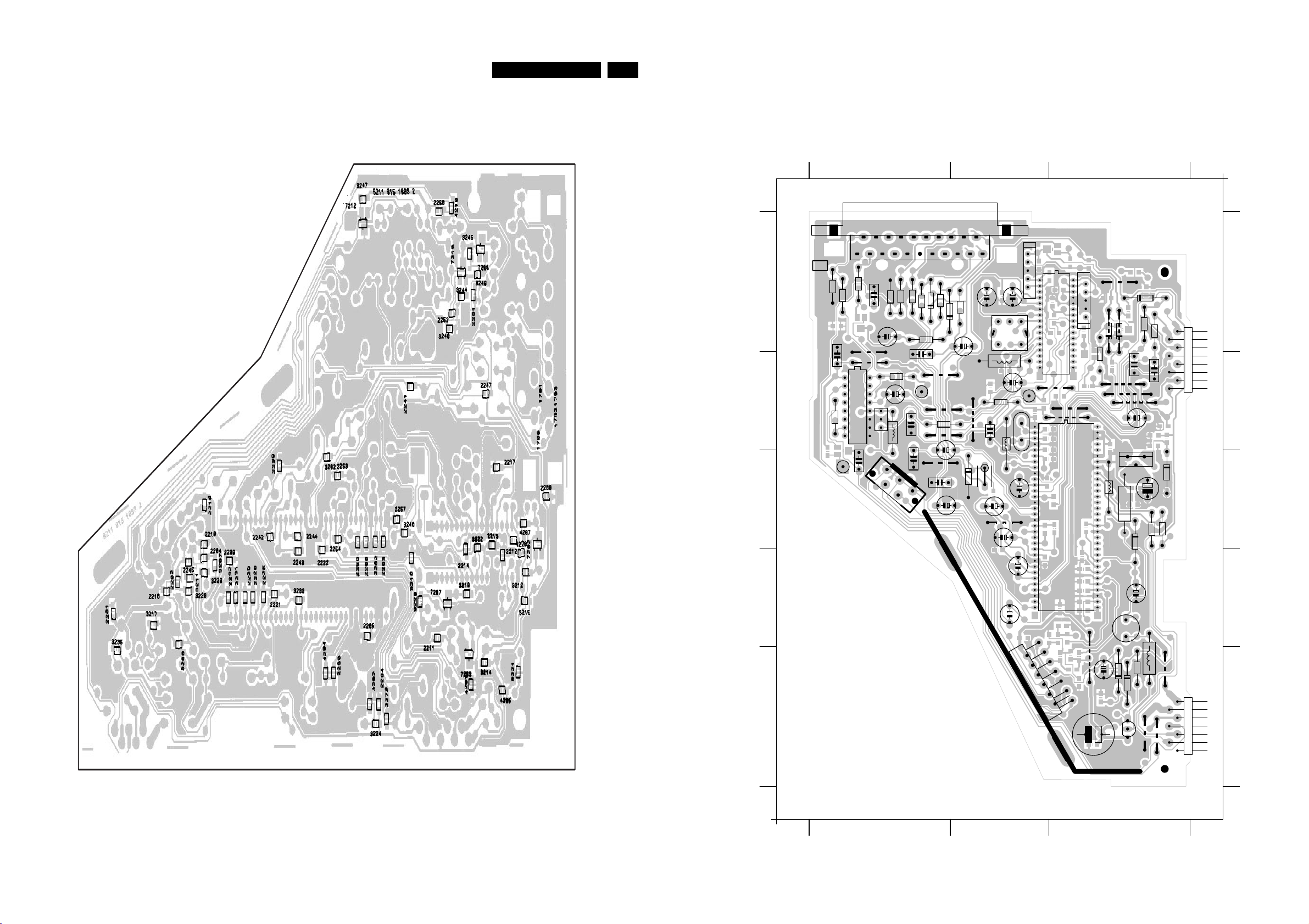
7 Electrical diagrams and print lay-outs
3
5
18Comet
9230 B 2
9231 A 2
9211 C 5
9220 C 2
9201 C 2
9202 C 2
7204 C 3
7205 B 4
6224 C 4
6225 C 3
5203 B 1
5204 C 4
4202 C 2
4204 C 3
3240 A 1
3241 A 1
3227 A 1
3228 C 5
3218 B 2
3219 C 1
3208 C 5
3209 A 2
2263 B 2
2273 C 2
2251 A 3
2252 A 1
2242 B 4
2243 C 3
2233 C 2
2234 C 2
2224 C 4
2225 C 4
2215 B 2
2216 C 5
2206 C 2
2207 C 2
9223 C 2
9224 C 2
9203 C 2
9205 C 2
7206 C 1
7207 C 2
6226 C 5
6227 A 1
5206 C 3
5207 B 2
4205 C 1
4207 B 1
3242 A 1
3243 A 1
3229 C 4
3230 B 1
3220 C 2
3221 C 1
3211 C 5
3212 C 1
3200 C 5
3201 C 3
2254 B 3
2255 C 5
2244 B 3
2245 C 5
2235 B 3
2236 A 3
2226 B 3
2227 B 4
2217 B 1
2218 B 1
2208 B 2
2209 C 4
9225 A 3
9226 B 2
9206 C 4
9207 B 3
7210 A 1
7211 A 2
6228 A 1
6229 C 5
5208 B 2
6220 C 1
4208 C 1
4210 A 1
3244 A 1
3245 A 1
3231 C 3
3232 C 3
3222 C 1
3223 B 3
3213 C 2
3214 C 1
3202 B 3
3203 C 1
2256 B 3
2257 B 2
2246 A 2
2247 B 3
2237 A 3
2238 B 4
2228 C 4
2229 C 4
2219 B 4
2220 B 1
2210 B 4
2211 C 2
9227 B 2
9228 A 2
9208 C 1
9209 C 5
7212 A 3
7221 C 2
7201 C 5
7202 C 1
6221 B 3
6222 C 1
4211 B 2
5201 A 3
3246 B 2
3247 A 3
3233 C 3
3234 A 1
3224 C 2
3225 B 2
3215 C 1
3216 C 2
3204 C 1
3205 A 2
2258 B 2
2259 B 3
2248 A 2
2249 A 1
2239 B 4
2240 B 3
2230 C 3
2231 C 4
2221 C 4
2222 C 3
2212 C 1
2213 C 1
9229 B 2
9210 C 5
9200 C 2
7203 C 1
6223 C 1
5202 C 1
3248 B 2
3239 A 1
3226 A 1
3217 C 5
3207 C 4
2262 B 2
2250 A 2
2241 B 1
2232 C 4
2223 A 2
2214 C 1
12345
C
3242
ST MOD 3W
A
0131
21
3243
3241
2250
3205
2249
9228
2252
9231
1
16
7211
1203
13
5201
8
9
2251
00021
2
AK
3234
3239
3240
3227
3245
2246
3209
00031
2223
2248
1
2237
5
4
71
0
0
1701
AK
6228
3226
3230
6227
2241
9230
9227
3218
9229
2247
9225
6221
2236
2226
B
17021703
220
1700
1
2218
9226
2258
AK
3223
2240
2235
2220
5203
1234
5208
6
2215
3225
1221
5207
1
1200
32
5
7
7206
17
0004
64
2256
9207
2238
33
2227
1
2
2
1
5
1
1201
15
16
9224
9202
9203
7221
9206
3
1
1
0
2
7
8211 015 1083
C
9208
6222
K
6220
AK
AK
9220
3213
6223
9223
9200
9201
1
2233
E
5206
3201
6224
32
1202
AK
3200
2255
6229
6226
AK
2203
EBC
A
0020
3203
2206
9205
7204
B
C
3231
AK
2224
9209
1
3204
2
2207
7
8
6225
AK
2200
3232
9210
5204
1
26
0065
9211
7
12
4
8.6532029_007.ai
140598
1202 C 4
0002 A 3
1203 A 2
0003 A 2
1221 B 2
0004 B 2
2200 C 3
0020 C 1
2201 C 5
0065 C 5
2202 C 5
0071 A 3
2203 C 5
2204 C 4
0131 B 1
1200 B 1
2205 C 2
1201 C 1
A
B
C
Page 34
7 Electrical diagrams and print lay-outs
19Comet
CL 86532029_008.eps
240698
Page 35
7 Electrical diagrams and print lay-outs
20Comet
1
H
G
F
2
3
4
5
6
7
8
9
10
H
G
F
E
D
C
B
E
D
C
B
A
1
2
3
4
5
6
7
8
9
10
A
Page 36
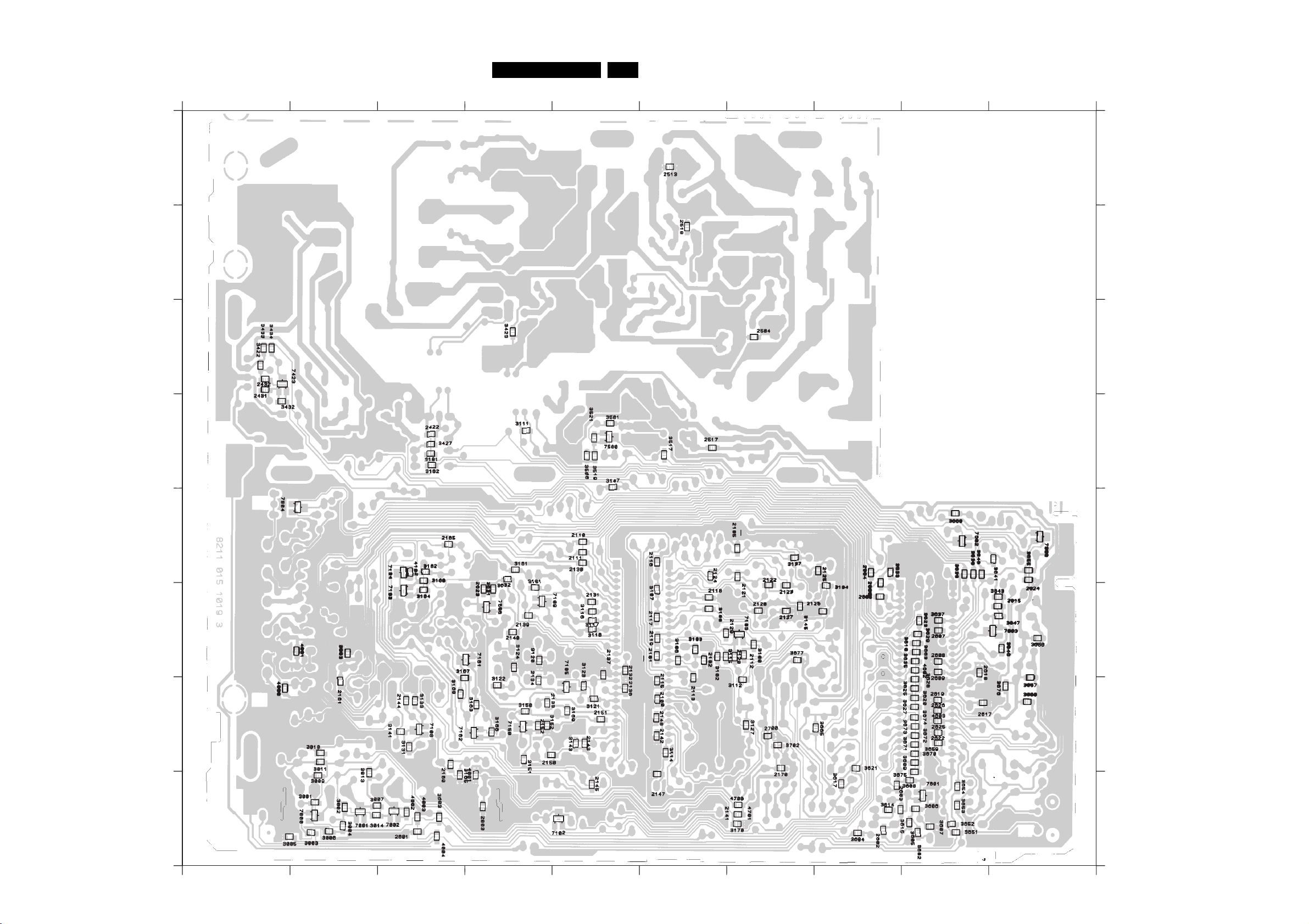
7 Electrical diagrams and print lay-outs
21Comet
1
H
G
F
2
3
4
5
6
7
8
9
10
H
G
F
E
D
C
B
E
D
C
B
A
1
2
3
4
5
6
7
8
9
10
A
Page 37
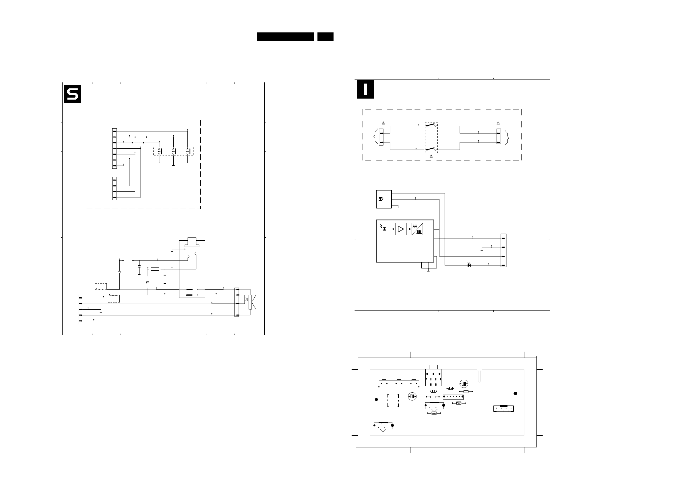
7 Electrical diagrams and print lay-outs
22Comet
0025 C 5
0042 C 2
0066 B 2
0071 G 1
A
B
C
D
E
F
G
H
TO
STEREO
MODULE
0072 G 6
1800 G 5
2800 F 3
2801 G 4
SEP CONTROLE
TO 0066
CHASSIS LOW
0071
+R
1
-R
2
A020
3
-L
4
A014
+L
5
*
2802 G 2
2803 G 3
3800 F 3
3801 G 4
1
2
3
4
5
6
7
0042
1
2
3
4
9800
*
5800
RES
A011
*
GNDA
5800 G 2
5801 G 2
9800 G 2
9801 B 3
9802 B 3
9804 H 2
A001 F 2
A002 F 3
0066
A021
A009
3800
270
100u
9802
A008
9801
A007
2800
GNDA
A002
330p
A022
A010
A001 A012
2802
5801
RES
9804
2803
3801
270
100u
A017
A003 G 4
A004 B 5
A005 B 4
A006 B 4
451 6723
A005
A006
3
5
4
6
GNDC
GNDA
A016
2801
330p
GNDA
A003
A17_
451 6723
A007 B 3
A008 B 3
A009 C 3
A010 C 3
A004
1
2
A011 G 2
A012 F 4
A013 G 6
A014 H 2
0025
A015 G 6
A016 F 4
A017 G 4
A018 H 6
A019 H 6
A020 H 1
A021 B 3
A022 B 3
1
2
3
1800
Headphone
4
78
5
A015
A019
A018
A013
0072
*
1
3
+
R
4
-
2
86532002_017.ai
+
-
180598
0022 A 3
0041 E 6
0050 B 6
0052 B 1
1600 D 1
6600 F 5
A001 D 3
A002 B 2
A003 B 2
A004 B 5
A005 B 5
A006 F 5
A007 E 5
A008 F 5
451 6723
A
B
C
D
E
F
A
0022
0052
B
1
2
A003
A3_
A002
A2_
MAIN-SWITCH
43
12
A004
A005
A4_
A5_
0050
2
1
TO
CHASSIS
L 6.2
C
1600 TFMS 5360
2
D
OUT
GND
Vs
3
1
E
F
INFRA RED RECEIVER
GNDC
A001
A1_
VDD
VSS
87
GNDC
4
5
6
A007
A7_
GNDC
6600
A006
A008
A6_
A8_
RC5
LED
0041
1
2
3
4
TO
CTRL GR3
L 6.2
A
B
C
D
E
F
G
G
L
H
0025 A 2
0066 A 4
0072 A 2
2800 A 2
2802 A 1
3800 A 2
0042 A 1
0071 A 2
1800 A 2
2801 A 2
2803 A 3
3801 A 3
5800 A 2
5801 A 3
451 6723
9800 A 2
9802 A 1
9801 A 1
9804 A 3
86532002_018.ai
G
180598
1234
1
1800
5
16
MT1MT2
9802
9801
AA
4
0042
123
2802
2
2800
3800
0072
432
5800
9800
8
3
1
2803
3801
2801
1
5
0071
9804
5801
0066
17
26
1234
Page 38
38 Comet
12 Spare parts list
12 Spare parts list
Chassis
Various
4822 212 11728 AUDIO NI- I :PCB
4822 212 11729 AUDIO NI-BG :PCB
4822 212 11731 AUDIO NI-L :PCB
4822 212 10522 PR.CIRCUIT, T.V
4822 212 10523 PR.CIRCUIT, T.V
4822 212 10524 CRT MODULE 20"
4822 310 10663 ES7062
∆ 4822 256 92053 HOLDER, PLASTIC
∆ 4822 265 11253 FUSE HOLDER 2P
4822 264 40207 3P MALE FOR BTB-
∆ 4822 265 30389 2P MALE
∆ 4822 265 10438 CONNECTOR 2P
∆ 4822 265 40596 2P MALE
∆ 4822 265 30389 2P MALE
4822 267 50621 7P MALE WHITE
4822 264 40239 3-F
4822 265 10452 CON.BM EURO H
4822 265 10703 CONN. EURO 21P
∆ 4822 265 11253 FUSE HOLDER 2P
4822 492 70871 SPRING
∆ 4822 502 13712 TORX SCREW 12X3
∆ 4822 255 70306 CONNECTOR, PICT
∆ 4822 255 70261 CRT SOCKET FL1
1000∆ 4822 210 10464 U943C/IEC
1001 4822 242 70936 OFWJ1952
1001 4822 242 81436 OFWK3953M
4822 402 10184 LED SUPPORT
1060 4822 276 13066 SKHVBB
1060 4822 276 13775 SWITCH
1061 4822 276 13066 SKHVBB
1061 4822 276 13775 SWITCH
1062 4822 276 13066 SKHVBB
1100 4822 242 10692 L1101-95260-0E3
1101 4822 242 70279 SFE6,0MB
1102 4822 242 81572 TPS6,0MB-TF21
1300∆ 4822 252 51175 19398E1(2,500A)
1501∆ 4822 070 32502 21802.5(2.5A)
1502∆ 4822 252 51185 19398E1(0,630A)
1503∆ 4822 252 51175 19398E1(2,500A)
1600 4822 130 91478 TSOP1736KD1
MODULE
MODULE
MODULE
WTB
MALE
21P
(4,433619MHz )
g
2000∆ 4822 124 40196 220µF 20% 16V
2001 4822 124 41643 100µF 20% 16V
2001 4822 124 80791 470µF 16V 20% 85C
2002 4822 126 13473 220nF 80-20% 50V
2005 4822 121 42408 220nF 5% 63V
2100∆ 5322 126 10223 4.7nF 10% 63V
2101 4822 126 12105 33nF 5% 63V
2101 4822 126 13473 220nF 80-20% 50V
2102∆ 5322 126 10223 4.7nF 10% 63V
2103 4822 124 40756 1µF 20% 100V
2104 4822 124 11529 16V 47µF 20%
2105∆ 4822 122 33177 10nF 20% 50V
2106∆ 4822 124 40433 47µF 20% 25V
2106 4822 124 80195 470µF 20% 10V
2107∆ 4822 124 41579 10µF 20% 50V
2108 4822 124 40756 1µF 20% 100V
2109 4822 121 51252 470nF 5% 63V
2110∆ 4822 126 10002 100nF 20% 25V
2111∆ 4822 126 10002 100nF 20% 25V
2112 4822 122 33175 2.2nF 20% 50V
2112 4822 122 33806 820pF 10% 63V
2112 4822 122 33891 3.3nF 10% 63V
2113∆ 4822 122 33177 10nF 20% 50V
2114 4822 121 41854 150nF 5% 63V
2116∆ 4822 126 10002 100nF 20% 25V
2117∆ 5322 126 10223 4.7nF 10% 63V
2118 4822 126 13689 18pF 1% 63V
2119 4822 126 13061 220nF 20% 25V
2120 4822 122 33175 2.2nF 20% 50V
2121∆ 4822 122 33177 10nF 20% 50V
2122∆ 4822 122 33177 10nF 20% 50V
2123∆ 4822 126 10002 100nF 20% 25V
2124∆ 4822 126 10002 100nF 20% 25V
2125∆ 4822 122 33177 10nF 20% 50V
2129∆ 5322 122 34123 1nF 10% 50V
2130∆ 4822 126 10002 100nF 20% 25V
2131∆ 4822 122 33177 10nF 20% 50V
2132 4822 126 13061 220nF 20% 25V
2133 5322 126 10511 1nF 5% 50V
2134 4822 126 13692 47pF 1% 63V
2135∆ 5322 122 32654 22nF 10% 63V
2136∆ 4822 126 10002 100nF 20% 25V
2137∆ 4822 126 10002 100nF 20% 25V
2138 4822 126 13473 220nF 80-20% 50V
2139 4822 122 33797 47nF 20% 50V
DIM:6.3X11MM
DXH=8X11.5
2140 4822 122 33797 47nF 20% 50V
2141∆ 4822 126 10002 100nF 20% 25V
2142∆ 4822 126 10002 100nF 20% 25V
2143 4822 122 32139 12pF 2% 63V
2144 4822 126 13061 220nF 20% 25V
2145 5322 126 10465 3.9nF 10% 50V
2146 4822 124 40763 2.2µF 100 V
2147∆ 4822 122 33177 10nF 20% 50V
2148∆ 5322 126 10223 4.7nF 10% 63V
2161 4822 126 13061 220nF 20% 25V
2170 5322 122 31865 1.5nF 10% 63V
2300 5322 122 31863 330pF 5% 50V
2300 5322 122 32268 470pF 10% 50V
2310 4822 122 33216 270pF 5% 50V
2310 5322 122 31863 330pF 5% 50V
2320 5322 122 31863 330pF 5% 50V
2320 5322 122 32268 470pF 10% 50V
2329 4822 121 43526 47nF 5% 250V
2330 4822 124 11531 50V 220µF 20%
2330 4822 124 40201 1000µF 20% 16V
2333∆ 4822 126 12171 3.3nF 20% 1KV
2333∆ 4822 126 13451 2.2nF 10% 2KV
2400 5322 122 32268 470pF 10% 50V
2401 4822 124 80064 680µF 20% 50V
2402 4822 124 40243 1.5µF 20% 63V
2403∆ 5322 122 32654 22nF 10% 63V
2403∆ 5322 126 10223 4.7nF 10% 63V
2404∆ 4822 122 33177 10nF 20% 50V
2404 4822 126 14087 100nF 10% 63V
2405 4822 122 33175 2.2nF 20% 50V
2420 4822 121 10513 1KV 7N5 5%
2420 4822 124 80676 4.7µF 20% 160V
2421 4822 121 51319 1µF 10% 63V
2422∆ 4822 121 42365 330nF 5% 250V
2422∆ 5322 122 32654 22nF 10% 63V
2423 4822 124 42336 47µF 20% 160V
2423∆ 4822 126 12269 680pF 10%) 2KV
2424 4822 124 80064 680µF 20% 50V
2425 4822 124 40214 1000µF 20% 25V
2425 4822 124 80064 680µF 20% 50V
2426 4822 124 80676 4.7µF 20% 160V
2427 5322 121 42489 33nF 5% 250V
2428 4822 121 51319 1µF 10% 63V
2429 5322 121 42661 330nF 5% 63V
2430 4822 121 42047 180nF 10% 250V
2431∆ 5322 126 10223 4.7nF 10% 63V
2432∆ 4822 122 33893 18nF 10% 63V
2500 4822 126 13597 330pF 10% 500V
2501∆ 4822 126 11524 1.5nF 10% 1KV
2501∆ 4822 126 14149 330pF 10%R 1KV
2502 4822 121 43856 4.7nF 5% 250V
2502 4822 121 51442 2.2nF 10% 50V
2503 4822 126 14153 2.2nF 10%B 1KV
2503 5322 121 42489 33nF 5% 250V
2504∆ 4822 126 11382 1nF 10% 1KV
2504∆ 5322 122 34123 1nF 10% 50V
2505∆ 4822 126 13594 2.2nF 20% 400V
2505∆ 4822 126 14037 2.2nF 20% 250V
2506 4822 121 43343 4.7nF 10% 400V
2507∆ 4822 121 10512 275V 220nF 20%
2508 4822 126 14153 2.2nF 10%B 1KV
2509 4822 126 14153 2.2nF 10%B 1KV
2510 4822 121 70162 10nF 5% 400V
2511 4822 124 81151 22µF 50V
2512∆ 4822 124 40196 220µF 20% 16V
2512 4822 124 40723 2200µF 20% 16V
2512 4822 124 80791 470µF 16V 20% 85C
2513 4822 126 13694 68pF 1% 63V
2514 4822 124 81139 2200µF 20% 16V
2514∆ 4822 124 81144 1000µF 16V
2515 4822 124 42336 47µF 20% 160V
2515 4822 124 81257 47µF 50/10% 200V
2516 4822 124 11532 400V 47µF 20%
2516 4822 124 11995 100µF 20% 400V
2517 4822 122 33837 1nF 10% 50V
2517∆ 5322 122 34123 1nF 10% 50V
2600∆ 4822 124 41579 10µF 20% 50V
2601 4822 126 13061 220nF 20% 25V
2602 4822 126 13061 220nF 20% 25V
2603 5322 126 10184 680P 5% 50V.
2604∆ 4822 126 10002 100nF 20% 25V
2605∆ 4822 126 10002 100nF 20% 25V
2606∆ 4822 126 10002 100nF 20% 25V
2608∆ 4822 126 10002 100nF 20% 25V
2608 5322 122 32448 10pF 5% 50V
2609∆ 4822 126 10002 100nF 20% 25V
2609 5322 122 32448 10pF 5% 50V
2610 4822 124 40769 4.7µF 20% 100V
2611 4822 124 40769 4.7µF 20% 100V
2612 4822 124 40769 4.7µF 20% 100V
2613 4822 124 40769 4.7µF 20% 100V
2614 4822 124 40769 4.7µF 20% 100V
2615∆ 5322 122 34123 1nF 10% 50V
2617 5322 122 32659 33pF 5% 50V
2618 5322 122 32659 33pF 5% 50V
2619∆ 4822 122 33177 10nF 20% 50V
2619∆ 5322 126 10223 4.7nF 10% 63V
2621 4822 124 40255 100µF 20% 63V
2622∆ 4822 122 33177 10nF 20% 50V
2624∆ 4822 126 10002 100nF 20% 25V
2625∆ 4822 126 10002 100nF 20% 25V
2626∆ 4822 126 10002 100nF 20% 25V
2700∆ 4822 126 10002 100nF 20% 25V
DXH=8X11.5
2801 4822 122 31175 1nF 10% 500V
2801 4822 126 13599 3.3nF 10% 500V
2802∆ 4822 126 13185 680pF 10% 500V
2803∆ 4822 124 41579 10µF 20% 50V
2803∆ 4822 126 10002 100nF 20% 25V
2808 4822 126 13597 330pF 10% 500V
2813∆ 4822 124 41579 10µF 20% 50V
f
3005∆ 4822 051 20472 4k7 5% 0.1W
3006∆ 4822 051 20472 4k7 5% 0.1W
3008 4822 116 52219 330Ω 5% 0.5W
3009 4822 117 12955 2k7 1% 0.1W 0805
3010 4822 117 10833 10k 1% 0.1W
3011∆ 4822 051 20472 4k7 5% 0.1W
3012∆ 4822 052 10399 39Ω 5% 0.33W
3012∆ 4822 052 10569 56Ω 5% 0.33W
3100 4822 051 20104 100k 5% 0.1W
3100 4822 051 20154 150k 5% 0.1W
3101 4822 117 10834 47k 1% 0.1W
3102 4822 051 20394 390k 5% 0.1W
3102 4822 051 20474 470k 5% 0.1W
3103∆ 4822 051 20153 15k 5% 0.1W
3104 4822 117 10833 10k 1% 0.1W
3105 4822 053 20275 2M7 5% 0.25W
3105 4822 053 20335 3M3 5% 0.25W
3105 4822 116 52234 100k 5% 0.5W
3106 4822 051 20684 680k 5% 0.1W
3107 4822 051 20104 100k 5% 0.1W
3108 4822 051 20822 8k2 5% 0.1W
3109 4822 116 52182 15Ω 5% 0.5W
3110 4822 116 52213 180Ω 5% 0.5W
3110 4822 116 52219 330Ω 5% 0.5W
3111 4822 051 10102 1k 2% 0.25W
3111 4822 051 20561 560Ω 5% 0.1W
3112 4822 051 20822 8k2 5% 0.1W
3113∆ 4822 051 20008 0Ω jumper . (0805)
3114∆ 4822 051 20008 0Ω jumper . (0805)
3114 4822 051 20331 330Ω 5% 0.1W
3114 4822 051 20479 47Ω 5% 0.1W
3115∆ 4822 051 20471 470Ω 5% 0.1W
3116∆ 4822 051 20101 100Ω 5% 0.1W
3117∆ 4822 051 20101 100Ω 5% 0.1W
3118∆ 4822 051 20101 100Ω 5% 0.1W
3119 4822 116 83878 270k 5% 0.5W
3120 4822 051 10102 1k 2% 0.25W
3121 4822 051 10102 1k 2% 0.25W
3122 4822 117 10353 150Ω 1% 0.1W
3122 4822 117 11503 220Ω 1% 0.1W
3123∆ 4822 051 20101 100Ω 5% 0.1W
3124 4822 117 11503 220Ω 1% 0.1W
3125 4822 050 11002 1k 1% 0.4W
3127 4822 051 20562 5k6 5% 0.1W 0805
3128 4822 051 20684 680k 5% 0.1W
3128 4822 116 52278 390k 5% 0.5W
3129 4822 100 11141 10k 30%lin 0.1W
3130 4822 101 11191 10k 30%LIN 0.1W
3131 4822 051 20394 390k 5% 0.1W
3132 4822 116 52228 680Ω 5% 0.5W
3133 4822 117 11448 180Ω 1% 0.1W
3134 4822 053 10479 47Ω 5% 1W
3134∆ 4822 053 10569 56Ω 5% 1W
3134 4822 053 10689 68Ω 5% 1W
3135 4822 116 52256 2k2 5% 0.5W
3136 4822 116 52175 100Ω 5% 0.5W
3136 4822 117 11504 270Ω 1% 0.1W
3137 4822 051 10102 1k 2% 0.25W
3138 4822 116 83872 220Ω 5% 0.5W
3139 4822 116 52269 3k3 5% 0.5W
3139 4822 116 83864 10k 5% 0.5W
3140 4822 116 52269 3k3 5% 0.5W
3141 4822 117 10353 150Ω 1% 0.1W
3142 4822 116 52251 18k 5% 0.5W
3143 4822 051 10102 1k 2% 0.25W
3144 4822 116 83868 150Ω 5% 0.5W
3144 4822 116 83883 470Ω 5% 0.5W
3145∆ 4822 051 20472 4k7 5% 0.1W
3146 4822 116 83872 220Ω 5% 0.5W
3147 4822 117 11507 6k8 1% 0.1W
3170 4822 117 11507 6k8 1% 0.1W
3180 4822 116 52289 5k6 5% 0.5W
3181 4822 117 12955 2k7 1% 0.1W 0805
3182∆ 4822 051 20153 15k 5% 0.1W
3300∆ 4822 053 11123 12k 5% 2W
3301 4822 051 20391 390Ω 5% 0.1W
3302 4822 117 11507 6k8 1% 0.1W
3303 4822 116 52176 10Ω 5% 0.5W
3303 4822 116 52197 56Ω 5% 0.5W
3304 4822 116 52207 1k2 5% 0.5W
3305 4822 116 83961 6k8 5%
3306 4822 101 11191 10k 30%LIN 0.1W
3307 4822 117 11896 1k5 20% 0.5W
3308 4822 101 11189 4.7k 30%LIN 0.1W
3309 4822 051 20689 68Ω 5% 0.1W
3310∆ 4822 053 11123 12k 5% 2W
3311 4822 117 11452 430Ω 1% 0.1W
3312 4822 117 11507 6k8 1% 0.1W
3313 4822 116 52176 10Ω 5% 0.5W
3313 4822 116 52197 56Ω 5% 0.5W
3314 4822 116 52207 1k2 5% 0.5W
3315 4822 116 52293 6k2 5% 0.5W
3316 4822 101 11191 10k 30%LIN 0.1W
3317 4822 117 11896 1k5 20% 0.5W
3318 4822 051 10102 1k 2% 0.25W
3319∆ 4822 051 20332 3k3 5% 0.1W
3319 4822 117 11449 2k2 1% 0.1W
3320∆ 4822 053 11123 12k 5% 2W
3321 4822 051 20391 390Ω 5% 0.1W
3322 4822 051 20562 5k6 5% 0.1W 0805
3323 4822 116 52176 10Ω 5% 0.5W
3323 4822 116 52197 56Ω 5% 0.5W
3324 4822 116 52263 2k7 5% 0.5W
3324 4822 116 52269 3k3 5% 0.5W
3325 4822 050 11002 1k 1% 0.4W
3326 4822 101 11191 10k 30%LIN 0.1W
3327 4822 117 11896 1k5 20% 0.5W
3330 4822 117 11896 1k5 20% 0.5W
3400 4822 051 20333 33k 5% 0.1W
3401 4822 051 20184 180k 5% 0.1W
3402∆ 4822 051 20471 470Ω 5% 0.1W
3403 4822 116 52195 47Ω 5% 0.5W
3403 4822 116 52199 68Ω 5% 0.5W
3404∆ 4822 052 10158 1Ω5 5% 0.33W
3405∆ 4822 052 11478 4Ω7 5% 0.5W
3406 4822 053 10182 1k8 5% 1W
3407 4822 101 11376 220Ω EVN-DJA
3408 4822 117 11383 12k 1% 0.1W
3409 4822 051 10102 1k 2% 0.25W
3410 4822 051 20393 39k 5% 0.1W
3411 4822 116 52289 5k6 5% 0.5W
3412 4822 116 52256 2k2 5% 0.5W
3420 4822 116 52244 15k 5% 0.5W
3420 4822 116 83864 10k 5% 0.5W
3421 4822 116 52244 15k 5% 0.5W
3421 4822 116 52303 8k2 5% 0.5W
3422 4822 117 12955 2k7 1% 0.1W 0805
3423 4822 051 10102 1k 2% 0.25W
3423 4822 051 20561 560Ω 5% 0.1W
3424∆ 4822 052 10109 10Ω 5% 0.33W
3424 4822 116 52195 47Ω 5% 0.5W
3425 4822 053 11129 12Ω 5% 2W
3426∆ 4822 053 11103 10k 5% 2W
3426∆ 4822 053 12153 15k 5% 3W
3427∆ 4822 051 20472 4k7 5% 0.1W
3427∆ 4822 052 11108 1Ω 5% 0.5W
3428∆ 4822 052 11108 1Ω 5% 0.5W
3430∆ 4822 052 11102 1k 5% 0.5W
3430 4822 116 52243 1k5 5% 0.5W
3431 4822 116 83883 470Ω 5% 0.5W
3432 4822 051 20225 2M2 5% 0.1W
3432 4822 051 20564 560k 5% 0.1W
3433 4822 051 20393 39k 5% 0.1W
3433 4822 117 11149 82k 1% 0.1W
3434 4822 051 20223 22k 5% 0.1W
3436∆ 4822 052 10151 150Ω 5% 0.33W
3437 4822 116 52283 4k7 5% 0.5W
3438 5322 116 53564 3Ω3 5% 0.5W
3439∆ 4822 052 10228 2Ω2 5% 0.33W
3500 4822 051 20331 330Ω 5% 0.1W
3500∆ 4822 051 20471 470Ω 5% 0.1W
3501∆ 4822 051 20101 100Ω 5% 0.1W
3502 4822 116 83864 10k 5% 0.5W
3502 4822 117 10833 10k 1% 0.1W
3503 4822 116 83864 10k 5% 0.5W
3503 4822 116 83961 6k8 5%
3504 4822 116 52219 330Ω 5% 0.5W
3504 4822 116 52249 1k8 5% 0.5W
3505 4822 116 52175 100Ω 5% 0.5W
3506 4822 117 12094 5% PR01
3507 4822 050 21302 1k3 1% 0.6W
3507 4822 050 21502 1k5 1% 0.6W
3508 4822 053 10682 6k8 5% 1W
3508 4822 117 12095 6k8 5%
3509 4822 116 52271 33k 5% 0.5W
3509 4822 116 83884 47k 5% 0.5W
3510 4822 117 12096 22k 1%
3510 4822 117 12707 33k 1% 1.3W
3511 4822 116 52263 2k7 5% 0.5W
3511 4822 116 52269 3k3 5% 0.5W
3512 4822 116 52291 56k 5% 0.5W
3512 4822 116 52297 68k 5% 0.5W
3513 4822 053 10334 330k 5% 1W
3514∆ 4822 052 10108 1Ω 5% 0.33W
3515∆ 4822 052 10108 1Ω 5% 0.33W
3516∆ 4822 116 40137 PTC 36Ω 365V
3516∆ 4822 116 40263 22Ω 276V 3k 25%
3516∆ 4822 117 12027 18Ω-3k 25%
3517 4822 051 10102 1k 2% 0.25W
3518 4822 116 52239 120k 5% 0.5W
3519 4822 051 20681 680Ω 5% 0.1W
3521 4822 117 11504 270Ω 1% 0.1W
3523∆ 4822 052 10338 3Ω3 5% 0.33W
3523∆ 4822 052 11338 3Ω3 5% 0.5W
3601 4822 116 52283 4k7 5% 0.5W
3602 4822 051 20223 22k 5% 0.1W
3603 4822 051 20104 100k 5% 0.1W
3604 4822 117 10833 10k 1% 0.1W
3605∆ 4822 051 20153 15k 5% 0.1W
3606 4822 051 20339 33Ω 5% 0.1W
3607 4822 051 20224 220k 5% 0.1W
3608 4822 117 10833 10k 1% 0.1W
3609∆ 4822 051 20332 3k3 5% 0.1W
3610 4822 116 83864 10k 5% 0.5W
3611 4822 116 83864 10k 5% 0.5W
3612 4822 116 52304 82k 5% 0.5W
3613 4822 116 83864 10k 5% 0.5W
Page 39
12 Spare parts list
39Comet
3614∆ 4822 051 20008 0Ω jumper . (0805)
3614 4822 117 10833 10k 1% 0.1W
3616 4822 050 11002 1k 1% 0.4W
3618 4822 117 11449 2k2 1% 0.1W
3619 4822 116 52252 180k 5% 0.5W
3620 4822 051 20394 390k 5% 0.1W
3621 4822 051 20394 390k 5% 0.1W
3622 4822 116 52175 100Ω 5% 0.5W
3622 4822 116 83864 10k 5% 0.5W
3623∆ 4822 051 20472 4k7 5% 0.1W
3624 4822 050 11002 1k 1% 0.4W
3625 4822 117 11449 2k2 1% 0.1W
3626 4822 050 11002 1k 1% 0.4W
3627∆ 4822 051 20472 4k7 5% 0.1W
3628∆ 4822 051 20472 4k7 5% 0.1W
3629∆ 4822 051 20472 4k7 5% 0.1W
3630 4822 116 83883 470Ω 5% 0.5W
3631∆ 4822 051 20471 470Ω 5% 0.1W
3632∆ 4822 051 20471 470Ω 5% 0.1W
3633 4822 051 20273 27k 5% 0.1W
3634 4822 050 11002 1k 1% 0.4W
3635∆ 4822 051 20472 4k7 5% 0.1W
3636 4822 116 83872 220Ω 5% 0.5W
3638 4822 117 11449 2k2 1% 0.1W
3639 4822 117 11449 2k2 1% 0.1W
3640 4822 117 11449 2k2 1% 0.1W
3641 4822 051 20392 3k9 5% 0.1W
3642 4822 116 52244 15k 5% 0.5W
3642 4822 116 52264 27k 5% 0.5W
3643∆ 4822 051 20472 4k7 5% 0.1W
3643 4822 051 20822 8k2 5% 0.1W
3644∆ 4822 051 20472 4k7 5% 0.1W
3644 4822 116 52283 4k7 5% 0.5W
3645 4822 116 52234 100k 5% 0.5W
3645 4822 116 83961 6k8 5%
3646 4822 051 20394 390k 5% 0.1W
3646∆ 4822 051 20471 470Ω 5% 0.1W
3646 4822 051 20681 680Ω 5% 0.1W
3647∆ 4822 051 20472 4k7 5% 0.1W
3647 4822 117 10833 10k 1% 0.1W
3648 4822 116 83864 10k 5% 0.5W
3649 4822 116 52195 47Ω 5% 0.5W
3650 4822 050 11002 1k 1% 0.4W
3651∆ 4822 051 20332 3k3 5% 0.1W
3652∆ 4822 051 20332 3k3 5% 0.1W
3653∆ 4822 051 20101 100Ω 5% 0.1W
3654∆ 4822 051 20101 100Ω 5% 0.1W
3655 4822 051 20122 1k2 5% 0.1W
3656∆ 4822 051 20472 4k7 5% 0.1W
3657∆ 4822 051 20472 4k7 5% 0.1W
3657 4822 116 52283 4k7 5% 0.5W
3658∆ 4822 051 20472 4k7 5% 0.1W
3658 4822 116 52283 4k7 5% 0.5W
3659∆ 4822 051 20472 4k7 5% 0.1W
3660 4822 116 52283 4k7 5% 0.5W
3661∆ 4822 053 10103 10k 5% 1W
3662 4822 116 52252 180k 5% 0.5W
3663 4822 051 20394 390k 5% 0.1W
3666 4822 050 11001 100Ω 1% 0.4W
3666 4822 116 52175 100Ω 5% 0.5W
3670 4822 117 11449 2k2 1% 0.1W
3671 4822 117 11449 2k2 1% 0.1W
3672 4822 117 11449 2k2 1% 0.1W
3673 4822 117 11449 2k2 1% 0.1W
3674 4822 117 11449 2k2 1% 0.1W
3675 4822 117 11449 2k2 1% 0.1W
3676 4822 117 10833 10k 1% 0.1W
3681 4822 050 11001 100Ω 1% 0.4W
3681 4822 050 11002 1k 1% 0.4W
3681 4822 116 52175 100Ω 5% 0.5W
3702∆ 4822 051 20153 15k 5% 0.1W
3800 4822 050 17509 75Ω 1% 0.4W
3800 4822 116 52201 75Ω 5% 0.5W
3801 4822 116 83868 150Ω 5% 0.5W
3801 4822 116 83883 470Ω 5% 0.5W
3802 4822 050 11203 12k 1% 0.4W
3802 4822 116 83961 6k8 5%
3803∆ 4822 051 20472 4k7 5% 0.1W
3804 4822 050 11001 100Ω 1% 0.4W
3804 4822 116 52175 100Ω 5% 0.5W
3804 4822 116 52202 82Ω 5% 0.5W
3805 4822 116 52283 4k7 5% 0.5W
3805 4822 116 80175 4k7 5% 0.5W
3806 4822 116 83872 220Ω 5% 0.5W
3807 4822 116 52219 330Ω 5% 0.5W
3808 4822 116 83961 6k8 5%
3810 4822 116 52219 330Ω 5% 0.5W
3811 4822 050 17509 75Ω 1% 0.4W
3811 4822 116 52201 75Ω 5% 0.5W
3812 4822 050 11002 1k 1% 0.4W
3813 4822 116 52175 100Ω 5% 0.5W
3813 4822 116 52176 10Ω 5% 0.5W
3813 4822 116 83883 470Ω 5% 0.5W
3815 4822 116 52219 330Ω 5% 0.5W
3816 4822 050 17509 75Ω 1% 0.4W
3816 4822 116 52201 75Ω 5% 0.5W
3817 4822 050 17509 75Ω 1% 0.4W
3817 4822 116 52201 75Ω 5% 0.5W
3820 4822 050 17509 75Ω 1% 0.4W
3820 4822 116 52201 75Ω 5% 0.5W
3825 4822 050 13901 390Ω 1% 0.4W
3825 4822 116 52226 560Ω 5% 0.5W
4xxx 4822 051 10008 0Ω 5% 0.25W (1206)
4xxx 4822 051 20008 0Ω 5% 0.25W (0805)
b
5100 4822 157 63068 0.28µH
5102 4822 157 61898 COIL
5103 4822 157 60123 6.8µH
5330 4822 156 21334 6µH
5420 4822 157 50965 IND FXD SPT0406A
5420∆ 4822 157 51462 10µH
5421 4822 157 10419 100U 10% 8RHB
5422∆ 4822 140 10562 ELDOR LOT
5422∆ 4822 140 10623 LOT 25"/28"
5423 4822 157 71401 27µH
5500∆ 4822 146 10461 SMPS-
5500∆ 4822 157 11306 FXC DOWN
5504 4822 157 53348 COIL
5505 4822 157 70826 2.4µH
5600 4822 242 10685 L1101-96019-0E1
5600 4822 242 73769 CST4.19mH z W
5601∆ 4822 157 53906 47µH
5602 4822 157 63507 0.18µH
5603 4822 157 63507 0.18µH
5604 4822 157 63507 0.18µH
15U PM10 A
1392.0001
TRANSFORMER
CONVERTER -
CU20C2
(12mH z )
d
6100∆ 4822 130 30621 1N4148
6101∆ 4822 130 30621 1N4148
6102∆ 4822 130 30621 1N4148
6103∆ 4822 130 30621 1N4148
6104 4822 130 34233 BZX79-B5V1
6106 4822 130 34167 BZX79-B6V2
6106∆ 4822 130 34173 BZX79-B5V6
6107 4822 130 34382 BZX79-B8V2
6108 4822 130 30861 BZX79-B7V5
6330∆ 4822 130 30621 1N4148
6420 4822 130 42488 BYD33D
6420∆ 4822 130 42489 BYD33G
6421 4822 130 42488 BYD33D
6422 4822 130 42488 BYD33D
6423∆ 4822 130 32896 BYD33M
6424 4822 130 42488 BYD33D
6426 4822 130 34145 BZX79-B39
6427 4822 130 42488 BYD33D
6500 4822 130 34233 BZX79-B5V1
6501∆ 4822 130 34173 BZX79-B5V6
6502 4822 130 34281 BZX79-B15
6503 4822 130 32245 BYV10-40
6503 4822 130 42488 BYD33D
6504 4822 130 41487 BYV95C
6504 4822 130 41601 BYV95A
6506 4822 130 70021 S1NB60
6507 4822 130 42488 BYD33D
6507 5322 130 31938 BYV27-200
6510∆ 4822 130 34197 BZX79-B12
6510 4822 130 34281 BZX79-B15
6514 5322 130 31932 BZT03-C200
6514 5322 130 83584 BZT03-C130
6600 4822 130 82037 HZT33
6601 4822 130 10859 TLDR5400
6601∆ 4822 209 30563 TLXR5400
6602∆ 4822 130 30621 1N4148
6800∆ 4822 130 31024 BZX79-B18
ce
7100 4822 209 12633 TDA8361K/N4
7100 4822 209 13047 TDA8361/N5-S7
7103 5322 130 42755 BC847C
7105 4822 130 60511 BC847B
7105∆ 5322 130 41982 BC848B
7107 4822 209 12635 TDA4665/V4
7108 5322 130 42136 BC848C
7109 4822 130 60511 BC847B
7109∆ 5322 130 41982 BC848B
7300 4822 130 41782 BF422
7310 4822 130 41782 BF422
7320 4822 130 41782 BF422
7400∆ 4822 130 40981 BC337-25
7401 4822 130 40917 BD238
7402 4822 130 40823 BD139
7420∆ 4822 130 10025 CNX82A
7421 5322 130 44647 BC368
7422∆ 4822 130 10025 CNX82A
7422∆ 4822 130 10206 BUT11AX
7423 5322 130 41983 BC858B
7424 4822 130 40937 BC548B
7500 5322 130 41983 BC858B
7501 4822 130 61675 BF487
7502 4822 130 41646 BF423
7504 4822 130 63725 STP4NA40FI
7505 4822 130 40937 BC548B
7505∆ 4822 130 41344 BC337-40
7600 4822 209 13085 IC DIG MOS U CO
7600 4822 209 15954 SAA5290ZP/072
7600 4822 209 16832 SAA5290PS/113
7600 4822 209 16828 SAA5290ZP/095
7601∆ 4822 209 73852 PMBT2369
7602 5322 130 60159 BC846B
7603 4822 130 60511 BC847B
7603∆ 5322 130 41982 BC848B
7604 4822 130 60511 BC847B
7604∆ 5322 130 41982 BC848B
7605 4822 209 12948 ST24C02B6
7605 4822 209 62098 ST24C02CB1
7606 4822 130 60511 BC847B
7606∆ 5322 130 41982 BC848B
7608 4822 130 60511 BC847B
7608∆ 5322 130 41982 BC848B
7700∆ 4822 209 60956 TDA7052/N2
7804 4822 130 60511 BC847B
7804∆ 5322 130 41982 BC848B
∆ 4822 267 31858 1 P
4822 267 51033 SINGLE
CONNECTOR
Control panel
Various
4822 212 10539 MOD SEP
4822 276 30422 SWITCH (3X ASSY)
∆ 4822 276 13592 MAINS U-GAP
4822 265 10417 ECO-DUO 2,5 4P-
∆ 4822 265 10438 CONNECTOR 2P
∆ 4822 265 40596 2P MALE
4822 267 50621 7P MALE WHITE
4822 265 31245 4P DUO 2,5
1800 4822 267 31014 HEADPHONE
CONTROL
2,5X4
MALE
SOCKET
g
2800 4822 126 13597 330pF 10% 500V
2801 4822 126 13597 330pF 10% 500V
2802 4822 124 41643 100µF 20% 16V
2803 4822 124 41643 100µF 20% 16V
DIM:6.3X11MM
DIM:6.3X11MM
f
3800 4822 116 83876 270Ω 5% 0.5W
3801 4822 116 83876 270Ω 5% 0.5W
4822 266 20073 2 FOLD
4822 265 30581 MKF17365- 5P
Mechanics
Various
1 4822 426 10693 BACKCOVER
2 4822 240 10105 LOUDSPEAKER (25
3 4822 402 10181 FIXATION
4 4822 454 13033 WINDOW 14”
5 4822 449 80276 CABINET 1465TS
5 4822 449 80277 CABINET 1445RS
6 4822 502 30739 CRT SCREW 14”
7 4822 462 10682 CRT PROT 14”
8 4822 157 11118 DEG COIL 14"
9 4822 410 10342 MAINS-KNOB
12 4822 464 10096 CHASSIS-GUIDE
4822 321 11367 MAINS CORD
4822 402 10179 CABLE BRACKET
4822 432 11269 BOTTOM PLATE
4822 454 13387 WORDMARK
4822 502 13886 PL2 X 6 SCREW
∆ 4822 276 13592 MAINS SWITCH
∆ 4822 265 10438 CONN 2P MALE
∆ 4822 265 40596 2P MALE
∆ 4822 502 13712 TORX SCREW 12X3
4822 303 91283 LOOP ANTENNA
4822 403 70972 LIGHT GUIDE
4822 462 11112 STAND ASSY 24"/
1986 4822 219 10555 RC8207/00
4822 442 01045 BATTERY LID
4822 131 11084 Picture tube
4822 131 11214 Picture tube
4822 131 11216 Picture tube
1 4822 458 50566 LEFTGRILL 25”
1445RS/1465TS
OHM - 1 W)
GOODMANS
29"
A34EAC01X15
A59EAK071X01
A66EAK071X01
1 4822 458 50568 LEFT GRILL 28”
1 4822 458 50567 RIGHT GRILL 25”
1 4822 458 50569 RIGHTGRILL 28”
2 4822 426 10689 BACKCOVER 25”
2 4822 426 10691 BACKCOVER 28”
3 4822 430 51024 CABINET 25"
3 4822 430 51025 CABINET 28"
8 4822 432 93386 DOOR 25”
8 4822 443 11042 DOOR 28”
10 4822 417 50252 LOCKING
12 4822 410 63857 MAINSKNOB
13 4822 492 32656 SPRING FOR
14 4822 380 20478 LIGHT GUIDEASSY
15 4822 505 10903 NUT+WASHER 28”
16 4822 404 30869 DEG.COIL
4822 267 30546 6P FEMALE
18 4822 240 90183 LOUDSPEAKER
20 4822 290 40288 MAINS SWITCH
23 4822 402 10771 CHASSIS BRACKET
4822 157 10664 25” DEG COIL
4822 157 71291 28" DEG COIL
4822 266 20073 2 FOLD CABLE
4822 290 40284 CON NBM V 3P F
4822 267 40794 3P FEMALE
∆ 4822 502 13712 TORX SCREW 12X3
4822 535 92924 CRT SCREW
4822 404 31308 CLAMP CRT
4822 404 31291 MAINS CORD
4822 267 30546 6P FEMALE
MECHANISM
MAINS KNOB
BRACKET
HOLDER
 Loading...