

Page 1

Philips Consumer Electronics
Technical Service Data
Service Solutions Group
Technical Publications Dept.
P.O. Box 555
401 East Old City Johnson Hwy.
Jefferson City, TN 37760
Manual 7583
Model no.: 25PT10C121
Chassis no.: 25F8
First Publish: 10-9-2000
Rev. Date: 3-21-2001
Print Date: 4/12/2003
TABLE OF CONTENTS
General Information
Training Information
Mechanical Assembly/Disassembly
Mechanical Diagrams
Mechanical Adjustments
Electrical Adjustments
Schematic Diagrams and PCBs
Scope Patterns
Troubleshooting
Service Bulletins and Important Information
Parts List
REFER TO SAFETY GUIDELINES
SAFETY NOTICE: ANY PERSON ATTEMPTING TO SERVICE THIS CHASSIS MUST FAMILIARIZE
HIMSELF WITH THE CHASSIS AND BE AWARE OF THE NECESSARY SAFETY PRECAUTIONS
TO BE USED WHEN SERVICING ELECTRONIC EQUIPMENT CONTAINING HIGH VOLTAGES.
CAUTION: USE A SEPARATE ISOLATION TRANSFORMER FOR THIS UNIT WHEN SERVICING
Visit our World Wide Web Site at http://www.magnavox.com
PDF created with FinePrint pdfFactory trial version http://www.pdffactory.com
Page 2

Philips Consumer Electronics
Technical Service Data
Service Solutions Group
Technical Publications Dept.
P.O. Box 555
401 East Old City Johnson Hwy.
Jefferson City, TN 37760
Manual 7583
Model no.: 25PT10C121
Chassis no.: 25F8
First Publish: 10-9-2000
Rev. Date: 3-21-2001
Print Date: 4/12/2003
General Information
REFER TO SAFETY GUIDELINES
SAFETY NOTICE: ANY PERSON ATTEMPTING TO SERVICE THIS CHASSIS MUST FAMILIARIZE
HIMSELF WITH THE CHASSIS AND BE AWARE OF THE NECESSARY SAFETY PRECAUTIONS
TO BE USED WHEN SERVICING ELECTRONIC EQUIPMENT CONTAINING HIGH VOLTAGES.
CAUTION: USE A SEPARATE ISOLATION TRANSFORMER FOR THIS UNIT WHEN SERVICING
Visit our World Wide Web Site at http://www.magnavox.com
PDF created with FinePrint pdfFactory trial version http://www.pdffactory.com
Page 3

F8 CHASSIS INTRODUCTION
The F8 chassis is a leader TV chassis produced by Philips Consumer Electronics
Company for the 1999 model year. The F8 chassis is used in sets with 25“ and
27“ screen sizes. The F8 chassis is a global design and is oriented front to rear, or
”north to south“, as it has been called. The F8 chassis tuning system features 181
channels with on-screen display (OSD). The main tuning system uses a tuner, a
microcomputer IC, and a memory IC mounted on the main chassis. The
microcomputer communicates with the memory IC, the customer keyboard,
remote receiver, U/V tuner, signal processor IC and the audio output IC via the
I2C bus. The memory IC retains the settings for favorite stations,
customer-preferred settings, and service/factory data.
The F8 chassis uses a Very Large Scale (VLSI) Integrated Circuit for signal
processing. This IC performs video IF, sound IF processing, AGC control, horizontal
and vertical drive and synchronization, also luminance/chrominance processing. The
on-screen graphics and closed caption decoding are done within the microprocessor,
and then sent to the signal processor IC to be added to the main signal.
The F8 chassis utilizes a switch mode power supply for the main voltage source.
The chassis has a hot chassis ground reference on the primary side of the power
supply, and a cold ground reference on the secondary side of the power supply
and the rest of the chassis. ALWAYS USE AN ISOLATION TRANSFORMER
WHEN SERVICING THIS CHASSIS FOR YOUR SAFETY.
MODEL TO MODULE LIST
The model to Module list shown below identifies all electrical panels, modules
and assemblies used in each model produced with the F8 chassis. This
information was current at time of printing.
Information concerning cabinet parts and cabinet mounted parts (CRT/Yoke/etc.)
is shown in the Cabinet Replacement Parts List.
Replacement part numbers for each module are provided in the Chassis Panel
Replacement Parts List.
If you are attempting to service a model equipped with the F8 chassis, the
necessary electrical information should be covered in this service manual, even if
the corresponding model number is not listed.
PDF created with FinePrint pdfFactory trial version http://www.pdffactory.com
Page 4

Model
Panel Number Size Description
PHILIPS – MAGNAVOX MODELS
00OCC925-C121 25“
00EMF891 A001 Main Chassis
00A10777-A001 Interface Module
00XR2503-C121 25“
00EMF801-A001, A002 Main Chassis
00TR2503-C121 25“
00EMF801-A001 Main Chassis
00HD2511-C121 25“
00EMF801-A001 Main Chassis
00XS2556-C121 25“
00EMF806-A001, A002 Main Chassis
00TS2556-C121 25“
00EMF806-A001, A002 Main Chassis
0025TS56-C121 25“
00EMF806-A001 Main Chassis
00TR2519-C121 25“
00EMF803-A001 Main Chassis
0025TR19-C121 25“
00EMF803-A001 Main Chassis
00TS2546-C121 25“
00EMF804-A001, A002 Main Chassis
00HD2530-C121 25“
00EMF804-A001 Main Chassis
00OCC927-C101 27“
00EMF893 A001, A102 Main Chassis
00A10777-A001 Interface Module
00TS2575-C121 25“
00EMF807-A001, A002 Main Chassis
00TS2774-C101 27“
00EMF833-A101, A102 Main Chassis
00TS2774-C121 27“
00EMF833-A102 Main Chassis
00TS2746-C101 27“
00EMF830-A101, A102 Main Chassis
00TS2746-C121 27“
PDF created with FinePrint pdfFactory trial version http://www.pdffactory.com
Page 5

00EMF830-A102 Main Chassis
PDF created with FinePrint pdfFactory trial version http://www.pdffactory.com
Page 6

00HD2720-C101 27“
00EMF830-A101 Main Chassis
or
00EMF831-A102
00XS2757-C101 27“
00EMF832-A101, A102 Main Chassis
00TS2757-C101 27“
00EMF832-A101 Main Chassis
0027TS57-C101 27“
00EMF832-A101, A102 Main Chassis
0027TS57-C121 27”
00EMF832-A102 Main Chassis
00TS3256-C101 32”
00EMF880-A102 Main Chassis
00TS3256-C121 32”
00EMF880-A002 Main Chassis
25” PHILIPS MODELS
0025PT10-C121 25”
00EMF803-A002 Main Chassis
0025PT15-C121 25”
00EMF806 A002 Main Chassis
PHILIPS – MAGNAVOX CARD SETS
00PC9225-C121 25“
00EMF891-A001, A102 Main Chassis
00A10777-A001 Interface Module
00TC9225-C121 25“
00EMF891-A001, A002 Main Chassis
00A10777-A001 Interface Module
PHILIPS - LATIN AMERICA
0026LL59-1121 25“
00EMF821-A001 Main Chassis
PHILIPS - LATIN AMERICA - AMV
0026LW59-3221 25“
00EMF823-A001 Main Chassis
0029LL69-1121 27“
00EMF851-A001 Main Chassis
PHILIPS LATIN AMERICA - 110V
0026LL59-0121 25“
00EMF820-A001, A002 Main Chassis
0026LW59-2221 25“
00EMF822-A001, A002 Main Chassis
PDF created with FinePrint pdfFactory trial version http://www.pdffactory.com
Page 7

0029LL69-0121 27“
00EMF850-A001, A002 Main Chassis
PHILIPS – INDUSTRIAL TELEVISION - SMARTPORT
00LL9125-C121 25”
00EMF899-A002 Main Chassis
00TL9125-C121 25“
00EMF890-A001, A002 Main Chassis
00PL9125-C121 25“
00EMF890-A001, A002 Main Chassis
00TL9127-C101 27“
00EMF892-A101, A102 Main Chassis
00CH1927-C101 27”
00EMF893-A102 Main Chassis
00A10680-B002 Channel One Card
00A10777-A001 Interface Module
00PA9027-C101 27”
00EMF894 A102 Main Chassis
00AVJ250 A001 Pro video Card Assembly
00A10757 A001 L9 Audio Jack Panel
00A10778 A001 L9 ITV Front A-V
00A10791 A001 Comb Filter Panel
00A10808 A001 Pro Plus Interface
00PL9127-C101 27“
00EMF892-A101, A102 Main Chassis
00PPC927-C101 27”
00EMF894 A102 Main Chassis
00A10791 A001 Comb Filter Panel
00A10757 A001 L9 Audio Jack Panel
00A10778 A001 L9 ITV Front A/V
00A10808 A001 Pro Plus Interface
00SCN927-C101 27”
00EMF894 A102 Main Chassis
00A10757 A001 L9 Audio Jack Panel
00A10777 A001 Interface Module
00A10778 A001 L9 ITV Front A/V
00A10791 A001 Comb Filter Panel
00PA9032-C101 32”
00EMF895 A102 Main Chassis
00AVJ250 A001 Pro video Card Assembly
00A10757 A001 L9 Audio Jack Panel
00A10791 A001 Comb Filter Panel
00A10808 A001 Pro Plus Interface
00PPC932-C101 32” Philips
00EMF895 A102 Main Chassis
00A10757 A001 L9 Audio Jack Panel
PDF created with FinePrint pdfFactory trial version http://www.pdffactory.com
Page 8
00A10791 A001 Comb Filter Panel
00A10808 A001 Pro Plus Interface
Remote
Replacement
Remote Drawing RC0702
00TR2503-C121 X
0025TR19-C121 X
0025TS56-C121 X
0026LL59-0121 X
0026LL59-1121 X
0026LW59-2221 X
0026LW59-3221 X
0027TS57-C101 X
0029LL69-0121 X
0029LL69-1121 X
00HD2511-C121 X
00HD2530-C121 X
00HD2720-C101 X
00TL9125-C121 X
00TL9127-C101 X
RC0702/04
3139 148
54201
RCO705/00
3139 228
80571
RC0705
-------------
RC282901/01
3139 228
81441
Philips
RCL9UB RCL9UB RCU82C
RC282901/04
3139 228
81451
PH/MX
RC2524/04
3139 228
81591
RC2528/04
3139 228
82051
RCU82D
-------------
PDF created with FinePrint pdfFactory trial version http://www.pdffactory.com
Page 9

00SCN932C101 32” Philips
00EMF895 A102 Main Chassis
00A10757 A001 L9 Audio Jack Panel
00A10777 A001 Interface Module
00A10791 A001 Comb Filter Panel
PHILIPS INDUSTRIAL TELEVISION - CARD SET
00PC9227-C101 27“ Philips
00EMF893-A101, A102 Main Chassis
00A10777-A001 Interface Module
SC2932C121 32" Philips
313501700770 Scan Card
00A10808 A001 Pro Plus Interface
00A10757 A001 Audio Jack Panel
00AVJ222 A001 Scan Converter Card
00A10654 A001 Scan Converter Jack Panel
00EMF895 A002 Main Chassis
00A10791 A001 Comb Filter Panel
Remote
Replacement
Remote Drawing RC0702
00TR2503-C121 X
0025TR19-C121 X
0025TS56-C121 X
0026LL59-0121 X
0026LL59-1121 X
0026LW59-2221 X
0026LW59-3221 X
0027TS57-C101 X
0029LL69-0121 X
0029LL69-1121 X
00HD2511-C121 X
00HD2530-C121 X
00HD2720-C101 X
00TL9125-C121 X
00TL9127-C101 X
00TR2519-C121 X
00TS2546-C121 X
00TS2556-C121 X
00TS2575-C121 X
RC0702/04
3139 148
54201
RCO705/00
3139 228
80571
RC0705
-------------
RC282901/01
3139 228
81441
Philips
RCL9UB RCL9UB RCU82C
RC282901/04
3139 228
81451
PH/MX
RC2524/04
3139 228
81591
RC2528/04
3139 228
82051
RCU82D
-------------
PDF created with FinePrint pdfFactory trial version http://www.pdffactory.com
Page 10

MODEL TO REMOTE CROSS-REFERENCE
Remote
Replacement
Remote Drawing RC0702
00TR2503-C121 X
0025TR19-C121 X
0025TS56-C121 X
0026LL59-0121 X
0026LL59-1121 X
0026LW59-2221 X
0026LW59-3221 X
0027TS57-C101 X
0029LL69-0121 X
0029LL69-1121 X
00HD2511-C121 X
00HD2530-C121 X
00HD2720-C101 X
00TL9125-C121 X
00TL9127-C101 X
00TR2519-C121 X
00TS2546-C121 X
00TS2556-C121 X
00TS2575-C121 X
00TS2746-C101 X
00TS2757-C101 X
00TS2774-C101 X
00XR2503-C121 X
00XS2556-C121 X
00XS2757-C101 X
00OCC925-C121
00OCC927-C101
00PC9225-C121
00PC9227-C101
00PL9125-C121
00PL9127-C101
00TC9225-C121
RC0702/04
3139 148
54201
No Remote
No Remote
No Remote
No Remote
No Remote
No Remote
No Remote
RCO705/00
3139 228
80571
RC0705
-------------
RC282901/01
3139 228
81441
Philips
RCL9UB RCL9UB RCU82C
RC282901/04
3139 228
81451
PH/MX
RC2524/04
3139 228
81591
RC2528/04
3139 228
82051
RCU82D
-------------
(Display Quick-Use Guide for RC0702 Transmitter)
(Display Quick-Use Guide for RCU82C Transmitter)
(Display Quick-Use Guide for RCL9UB Transmitter)
PDF created with FinePrint pdfFactory trial version http://www.pdffactory.com
Page 11

PDF created with FinePrint pdfFactory trial version http://www.pdffactory.com
Page 12

MODEL TO JACKPANEL CROSS-REFERENCE
(Display JP9000 Jack Panel)
(Display JP9103 Jack Panel)
(Display JP9106 Jack Panel)
Models Jack Panels
JP9000 JP9103 JP9106
00TR2503-C121
0025TR19-C121 X
0025TS56-C121 X
0026LL59-0121 X
0026LL59-1121 X
0026LW59-2221 X
0026LW59-3221 X
0027TS57-C101 X
0029LL69-0121 X
0029LL69-1121 X
00HD2511-C121 X
00HD2530-C121 X
00HD2720-C101 X
00TR2503-C121 X
00TR2519-C121 X
00TS2546-C121 X
00TS2556-C121 X
00TS2575-C121 X
00TS2746-C101 X
00TS2757-C101 X
00TS2774-C101 X
00XR2503-C121 X
00XS2556-C121 X
00XS2757-C101 X
00TL9125-C121
00TL9127-C101
00OCC925-C121
00OCC927-C101
00PC9225-C121
00PC9227-C101
00PL9125-C121
00PL9127-C101
00TC9225-C121
X
No Jack Panel
No Jack Panel
No Jack Panel
No Jack Panel
No Jack Panel
No Jack Panel
No Jack Panel
No Jack Panel
No Jack Panel
PDF created with FinePrint pdfFactory trial version http://www.pdffactory.com
Page 13

GLOSSARY OF TERMS, ACRONYMS, AND ABBREVIATIONS
2CS Two Channel Stereo
AFC Automatic Frequency Control
AFT Automatic Fine Tuning
AP Asia Pacific
ATS Automatic Tuning System
AV External Audio/Video
AVL Automatic Volume Level control
BTSC Broadcast Television Standard Committee (TV Stereo)
CBA Circuit Board Assembly (PCB)
CC Closed Captioning
CSM Customer Service Mode
CVBS Color Video Blanking Sync
DNR Dynamic Noise Reduction
EEPROM Electrical Erasable Programmable Read-Only Memory
Error Buffer Register that keeps track of errors that occur and stores error codes
Error Code A numerical value used to indicate a failure in the television
EU Europe
EXT External audio/video input
FM Frequency Modulation
I²C Inter IC bus, 2-wire bi-directional (SCL/SDA)
ID Identification
IDENT Horizontal coincidence signal, transmitter identification
IF Intermediate Frequency
IN ITT sound IC with NICAM function
IT ITT sound IC without NICAM function
LATAM Latin America
LED Light Emitting Diode
Local Keyboard The buttons (usually volume up, volume down, channel up, and channel down)
located on the front of the television set
MA Mono All; single mono carrier receiver
NR Noise Reduction
NTSC National Television Systems Committee (video)
NVM Non Volatile Memory
OB Option Byte (Feature Byte)
OSD On Screen Display
PCB Printed Circuit Board (CBA)
PIP Picture In Picture
PLL Phase Locked Loop
PP Personal Preference
RAM Random Access Memory
RC Remote Control
RC-5 Remote Control system 5
RGB Red Green Blue
ROM Read Only Memory
SAM Service Alignment Mode
SAP Second Audio Program
SCL Serial Clock
SDA Serial Data
SDM Service Default Mode
SVHS Super Video Home System
Top Level Menu This refers to the main menu (as opposed to sub menus) in SAM
V-Chip Violence-Chip
PDF created with FinePrint pdfFactory trial version http://www.pdffactory.com
Page 14

VCR Video Cassette Recorder
Y/C Luminance/Chrominance (video)
SAFETY INSTRUCTIONS FOR REPAIRS
1. Safety regulations require that during a repair:
• the set should be connected to the mains via an isolating transformer
• safety components, indicated by the symbol s , should be replaced by components
identical to the original ones
• when replacing the CRT, safety goggles must be worn
2. Safety regulations require that after a repair the set must be returned in its original
condition. In particular, attention should be paid to the following points:
Note:
This resoldering is advised to prevent bad connections due to metal fatigue in solder
joints, and is therefore only necessary for television sets older than 2 years.
• As a strict precaution, we advise you to resolder the solder joints through which the
horizontal deflection current is flowing, in particular:
- All pins of the line output transformer (LOT)
- flyback capacitor(s)
- S-correction capacitor(s)
- line output transistor
- pins of the connector with wires to the deflection coil
- other components through which the deflection current flows
• Resolder points are marked by a white circle on the bottom of the CBA.
• The wire trees and EHT cable should be routed correctly and fixed with the
mounted cable clamps.
• The insulation of the mains lead should be checked for external damage.
• The mains lead strain relief should be checked for its function in order to avoid
touching the CRT, hot components or heat sinks.
• The electrical DC resistance between the mains plug and the secondary side
should be checked (only for sets which have a mains isolated power supply).
This check can be done as follows:
- unplug the mains cord and connect a wire between the two pins of the mains
plug
- set the mains switch to the on position (keep the mains cord unplugged!)
- measure the resistance value between the pins of the mains plug and the
metal shielding of the tuner or the aerial connection on the set. The reading
should be between 4.5 Megohm and 12 Megohm.
- switch off the TV and remove the wire between the two pins of the mains plug
• The cabinet should be checked for defects to avoid touching of any inner parts by
the customer.
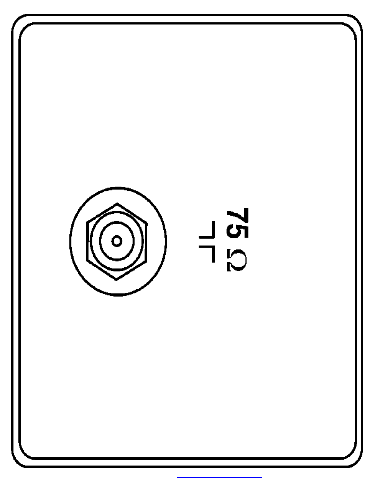
JP9000 JP9103 JP9106 JP9202 JP9204 JP9403 JP9406 JP9410 JP9411 JP9519 JP9523
RF Input/
Antenna
Jacks
Quantity
Video
Input
75 ohm 75 ohm 75 ohm 75 ohm 75 ohm 75 ohm 75 ohm 75 ohm 75 ohm 2 x 75
ohm
0 3 6 2 4 3 7 10 11 19 23
1 1 1 1 1 1 2 2 3 3
2 x 75
ohm
PDF created with FinePrint pdfFactory trial version http://www.pdffactory.com
Page 15

JACK PANEL DEFINITIONS
JP9000 JP9103 JP9106 JP9202 JP9204 JP9403 JP9406 JP9410 JP9411 JP9519 JP9523
RF Input/
Antenna
Jacks
Quantity
Video
Input
Audio
Input
SVHS
Input
ead-phon Front Front Front Front Side Side
Surround
Sound
Speaker
Video Out 1 1 1 1 1 1
Audio
Output
Smart
Plug
CH. 1
Demod.
Theft
Control
Pillow
Control
Guide +
Gold
YUV
Comp. In
"* Only one set of audio output jacks, menu selectable, switchable between fixed and variable output"
75 ohm 75 ohm 75 ohm 75 ohm 75 ohm 75 ohm 75 ohm 75 ohm 75 ohm 2 x 75
0 3 6 2 4 3 7 10 11 19 23
1 1 1 1 1 1 2 2 3 3
L-R L-R 1 L-R 1 L-R 2 (L-R) 2 (L-R) "3(L-R)
Out
L-R
(Fixed)
L-R
(Fixed)
L-R
(Fixed)
1 2
L-R
(Fixed)
ohm
2-Rear,
1-Side"
(1-Rear/
1-Side)
(1-Rear/
L-R* L-R*
1 1
3 3
2 x 75
ohm
"3(L-R)
2-Rear,
1-Side"
2
1-Side)
4
PDF created with FinePrint pdfFactory trial version http://www.pdffactory.com
Page 16

MAIN CHASSIS SCHEMATIC NOTES:
UNLESS OTHERWISE SPECIFIED:
1. ALL VOLTAGES AND WAVEFORMS WERE TAKEN UNDER THE FOLLOWING
CONDITIONS:
- LINE VOLTAGE MAINTAINED AT 120VAC, 60Hz VIA AN ISOLATION
TRANSFORMER.
- SET IN SDM (SERVICE DISPLAY MODE). To enter SDM, press 0-6-2-5-9-6-Menu
on the remote control.
- ALL VOLTAGES WERE TAKEN FROM MODEL TS2774C101.
2. ALL WAVEFORMS WERE TAKEN WITH AN NTSC SIGNAL GENERATOR
DELIVERING 10mVp-p AT THE ANTENNA INPUT.
3. ON VOLTAGE CHARTS:
- VOLTAGES IN THE "Signal" COLUMN WERE TAKEN WITH AN NTSC SIGNAL
GENERATOR DELIVERING 10mVp-p AT THE ANTENNA INPUT.
- VOLTAGES IN THE "No Signal" COLUMN WERE TAKEN WITH NO SIGNAL
APPLIED.
- VOLTAGES IN THE "Standby" COLUMN WERE TAKEN WITH THE SET IN
STANDBY MODE (Power supplied to the chassis, set turned off).
4. ALL VOLTAGES ARE POSITIVE DC WITH RESPECT TO GROUND IN THAT
SECTION OF THE CHASSIS, AND MAY VARY DUE TO NORMAL PRODUCTION
TOLERANCES.
5. COMPONENT AND SPECIAL SYMBOLS:
* INDICATES A COMPONENT WHICH WILL VARY DEPENDING ON SCREEN
SIZE, PRODUCTION DATES, AND OPTION FEATURES INSTALLED. PLEASE
SEE THE REPLACEMENT PARTS LIST FOR SPECIFIC PART INFORMATION.
• INDICATES A COMPONENT IS AN SMD ”CHIP“ TYPE COMPONENT, AND AS
SUCH WILL BE LOCATED ON THE BOTTOM Side OF THE CBA.
6. A HIGH VOLTAGE OSCILLOSCOPE PROBE (100:1) IS NEEDED TO MEASURE THE
WAVEFORM AT THE HORIZONTAL OUTPUT TRANSISTOR (PART # 7620).
7. SPARK GAPS SHOWN ON THE CRT SCHEMATIC ARE INTERNAL TO THE CRT
SOCKET.
8. THE NUMBERS 1a THROUGH 38b, SHOWN IN ENCLOSED BOXES,
CORRESPOND TO THE WAVEFORM PHOTOGRAPHS.
9. FOR VOLTAGE, WATTAGE, AND TOLERANCE RATINGS OF RESISTORS AND
CAPACITORS, PLEASE SEE THE ELECTRICAL REPLACEMENT PARTS LIST.
10. INDICATES PCE REPLACEMENT PART NUMBER ONLY.
MAIN CHASSIS WAVEFORM NOTES:
UNLESS OTHERWISE SPECIFIED:
ALL WAVEFORMS WERE TAKEN UNDER THE FOLLOWING CONDITIONS:
- LINE VOLTAGE MAINTAINED AT 120VAC, 60Hz VIA AN ISOLATION
TRANSFORMER.
- SET IN SDM (SERVICE DISPLAY MODE). TO ENTER SDM, PRESS
0-6-2-5-9-6-MENU ON THE REMOTE CONTROL.
- ALL WAVEFORMS WERE TAKEN FROM MODEL TS2774-C101.
- ALL WAVEFORMS WERE TAKEN WITH AN NTSC SIGNAL GENERATOR
DELIVERING 10mVp-p AT THE ANTENNA INPUT.
- SWEEP TIME/CM SETTINGS ARE SHOWN WITH THE FIGURES IN THE
CALIBRATED POSITION.
- THE ACTUAL SWEEP TIMES AND VOLTAGES PRESENT ARE SHOWN
WHEREVER POSSIBLE.
PDF created with FinePrint pdfFactory trial version http://www.pdffactory.com
Page 17

- COMPOSITE VIDEO SIGNALS ARE SHOWN WITHOUT SWEEP TIME AND
VOLTAGES PRESENT BECAUSE THESE SIGNALS HAVE VARIABLE SWEEP
TIMES AND VOLTAGES.
- A HIGH VOLTAGE OSCILLOSCOPE PROBE (100:1) IS NEEDED TO MEASURE
THE WAVEFORM AT THE HORIZONTAL OUTPUT TRANSISTOR (PART #
7460).
- THE DESIGNATORS A1a THROUGH V6c, SHOWN IN ENCLOSED BOXES,
CORRESPOND TO THE WAVEFORM PHOTOGRAPHS.
AUDIO WAVEFORM NOTES:
THESE NOTES APPLY ONLY TO THE AUDIO WAVEFORMS (A1a THROUGH A3d).
AUDIO WAVEFORMS WERE TAKEN UNDER THE FOLLOWING CONDITIONS:
- ALL WAVEFORMS WERE TAKEN WITH A LEADER LMS-238 SOUND
GENERATOR CONNECTED AT THE ANTENNA INPUT, WITH THE FOLLOWING
SETTINGS:
- INT FREQUENCY SET TO 1kHz
- STEREO (L+R), PILOT ON
- VIF/RF OUTPUT AT CHANNEL 3
- ALL WAVEFORMS WERE TAKEN FROM MODEL TS2774C101.
- TELEVISION SET TO CHANNEL 3 IN NORMAL MODE.
- DO NOT MUTE THE SET.
- SET THE TELEVISION VOLUME AT 40.
- THE SPEAKERS MAY BE DISCONNECTED AT CONNECTOR #0234 (BOARD
LOCATION B-1) IF THE AUDIO OUTPUT CAUSES A DISTRACTION TO THE
SERVICER.
F8 CHASSIS FEATURE LISTING
USA/CANADIAN CHASSIS LISTINGS
LATIN AMERICAN CHASSIS LISTINGS
INDUSTRIAL CHASSIS LISTINGS
PDF created with FinePrint pdfFactory trial version http://www.pdffactory.com
Page 18
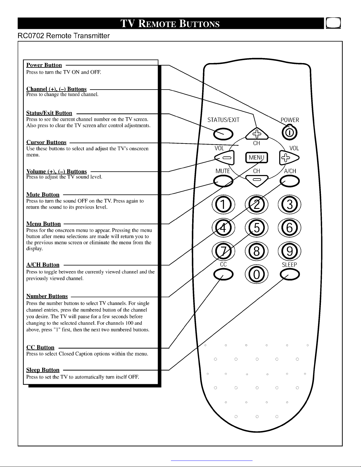
(Display Quick-Use Guide for RC0702 Transmitter)
PDF created with FinePrint pdfFactory trial version http://www.pdffactory.com
Page 19

(Display Quick-Use Guide for RCU82C Transmitter)
PDF created with FinePrint pdfFactory trial version http://www.pdffactory.com
Page 20
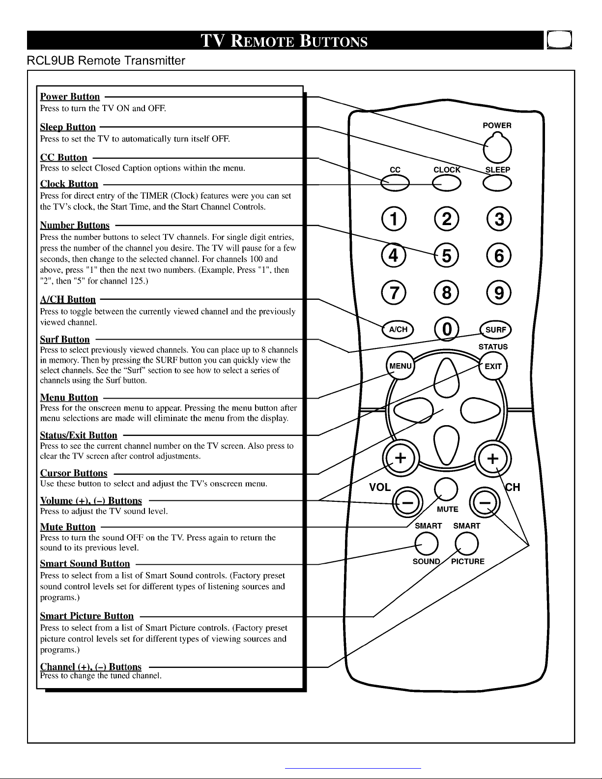
(Display Quick-Use Guide for RCL9UB Transmitter)
PDF created with FinePrint pdfFactory trial version http://www.pdffactory.com
Page 21
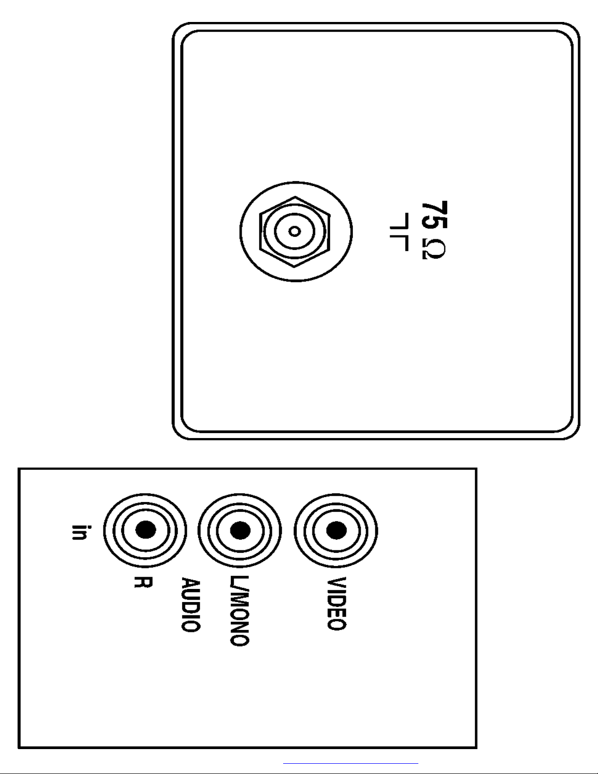
(Display JP9000 Jack Panel)
PDF created with FinePrint pdfFactory trial version http://www.pdffactory.com
Page 22
(Display JP9103 Jack Panel)
PDF created with FinePrint pdfFactory trial version http://www.pdffactory.com
Page 23

(Display JP9106 Jack Panel)
PDF created with FinePrint pdfFactory trial version http://www.pdffactory.com
Page 24

Philips Consumer Electronics
Technical Service Data
Service Solutions Group
Technical Publications Dept.
P.O. Box 555
401 East Old City Johnson Hwy.
Jefferson City, TN 37760
Manual 7583
Model no.: 25PT10C121
Chassis no.: 25F8
First Publish: 10-9-2000
Rev. Date: 3-21-2001
Print Date: 4/12/2003
Training Information
REFER TO SAFETY GUIDELINES
SAFETY NOTICE: ANY PERSON ATTEMPTING TO SERVICE THIS CHASSIS MUST FAMILIARIZE
HIMSELF WITH THE CHASSIS AND BE AWARE OF THE NECESSARY SAFETY PRECAUTIONS
TO BE USED WHEN SERVICING ELECTRONIC EQUIPMENT CONTAINING HIGH VOLTAGES.
CAUTION: USE A SEPARATE ISOLATION TRANSFORMER FOR THIS UNIT WHEN SERVICING
Visit our World Wide Web Site at http://www.magnavox.com
PDF created with FinePrint pdfFactory trial version http://www.pdffactory.com
Page 25

F8 CHASSIS INTRODUCTION
The F8 chassis is a leader TV chassis produced by Philips Consumer Electronics Company for the
1999 model year. The F8 chassis is used in sets with 25“ and 27“ screen sizes. The F8 chassis is a
global design and is oriented front to rear, or ”north to south“, as it has been called. The F8 chassis
tuning system features 181 channels with on-screen display (OSD). The main tuning system uses a
tuner, a microcomputer IC, and a memory IC mounted on the main chassis. The microcomputer
communicates with the memory IC, the customer keyboard, remote receiver, U/V tuner, signal
processor IC and the audio output IC via the I2C bus. The memory IC retains the settings for favorite
stations, customer-preferred settings, and service/factory data.
The F8 chassis uses a Very Large Scale (VLSI) Integrated Circuit for signal processing. This IC
performs video IF, sound IF processing, AGC control, horizontal and vertical drive and synchronization,
also luminance/chrominance processing. The on-screen graphics and closed caption decoding are
done within the microprocessor, and then sent to the signal processor IC to be added to the main
signal.
The F8 chassis utilizes a switch mode power supply for the main voltage source. The chassis has a hot
chassis ground reference on the primary side of the power supply, and a cold ground reference on the
secondary side of the power supply and the rest of the chassis. ALWAYS USE AN ISOLATION
TRANSFORMER WHEN SERVICING THIS CHASSIS FOR YOUR SAFETY.
SIGNAL FLOW DESCRIPTION
(Display Signal Flow Block Diagram)
The incoming RF signal is applied to the U/V tuner where the 45.75 MHz IF signal is developed and
amplified. The IF signal then exits the tuner from pin11to pass through the SAW filter, (1003). The
shaped signal is then applied to IC 7250, the IF processor. The automatic gain control (AGC) is
performed in IC 7250 and applied to the U/V tuner at pin1. An automatic fine tuning signal (AFT) is also
generated in the IC and then routed to the tuning system via the I2C bus, to provide frequency
correction as needed.
The IF signal exits IC 7250 at pin 6, the audio and video signals are separated and each processed
accordingly. The sound IF signal enters IC 7250 at pin 1, while the video re-enters at pin 13. The audio
signal passes through the pre-amp, volume control and volume limiting circuits before application to the
final audio stages.
The video signal entering at pin 13, is separated into its luminance and chrominance components, and
exits at pins 21, 20, and 19 as R, G, and B respectively. The R G B signals are sent to the CRT DRIVE
board, amplified and applied to the CRT pins as drive. Drive and cutoff controls for the CRT are also
located on this board.
Brightness, Picture, Sharpness, Color and Tint control voltages are varied by the microprocessor, IC
7600 through individual control lines. IC 7600 also controls selected inputs, as selected by the
consumer.
Video and audio muting are an internal function of IC 7250. Automatic volume limiting also takes place
inside this IC.
Vertical and Horizontal drive signals are also developed inside IC 7250. Vertical drive exits the IC from
pin 47, while Horizontal drive exits at pin 40. These signals are a product of a Voltage Controlled
Oscillator Circuit (VCO) and divider network located inside the chip. Vertical drive is applied to pin 1 of
IC 7401, amplified, shaped, and output from pin 5 where it is applied to the vertical winding of the yoke.
A feedback signal is returned to pin 46 of IC 7250. The vertical sync pulse is also applied to the
PDF created with FinePrint pdfFactory trial version http://www.pdffactory.com
Page 26

microprocessor, IC 7600, to pin 37 for On-Screen Display and Closed-Captioning synchronization. The
horizontal drive signal exits IC 7250 from pin 40 and is applied to Q 7461, the horizontal driver
transistor. The signal is amplified and coupled to the base circuit of Q 7460, the horizontal output
transistor. The H.O.T. drives the Integrated Flyback Transformer, which provides high voltage, screen
voltage, focus, G-2, and filament voltages for the CRT. A scan-derived power supply is also provided by
the IFT. It supplies -13 volts, +13 volts, +50 volts, a secondary +5 volt supply, and a +200 volt source for
video drive. The secondary of the IFT is monitored by safety circuits and is tied back to the
microprocessor and signal-processing IC’s to turn the set off if a problem should occur.
POWER SUPPLY DESCRIPTION
(Display Power Supply Block Diagram)
The F8 chassis family uses a free-running switch-mode power supply with a single controller IC. As AC
power is applied to the set, approximately 160volts DC is developed by the bridge rectifiers and fed to
the primary winding of the power transformer, then to the FET switch. The start voltage for the power
supply is taken from the hot leg of the AC input. This voltage goes to controller IC 7520. A separate
operating voltage is developed from the power transformer, rectified, and applied to IC 7520. The power
supply is on all the time; there is no standby mode. The set is turned on and off by the microprocessor
switching the +8 volt regulator on and off. The +8 volt is the supply voltage for the signal processor.
IC7520 is regulated by means of a feedback circuit, monitoring the +11 volt secondary line. Any voltage
variations are reflected back to the controller IC 7520 through an Opto-Coupler IC and change the
operating frequency of the power supply as needed. REMEMBER TO USE AN ISOLATION
TRANSFORMER WHEN SERVICING THIS CHASSIS.
PDF created with FinePrint pdfFactory trial version http://www.pdffactory.com
Page 27
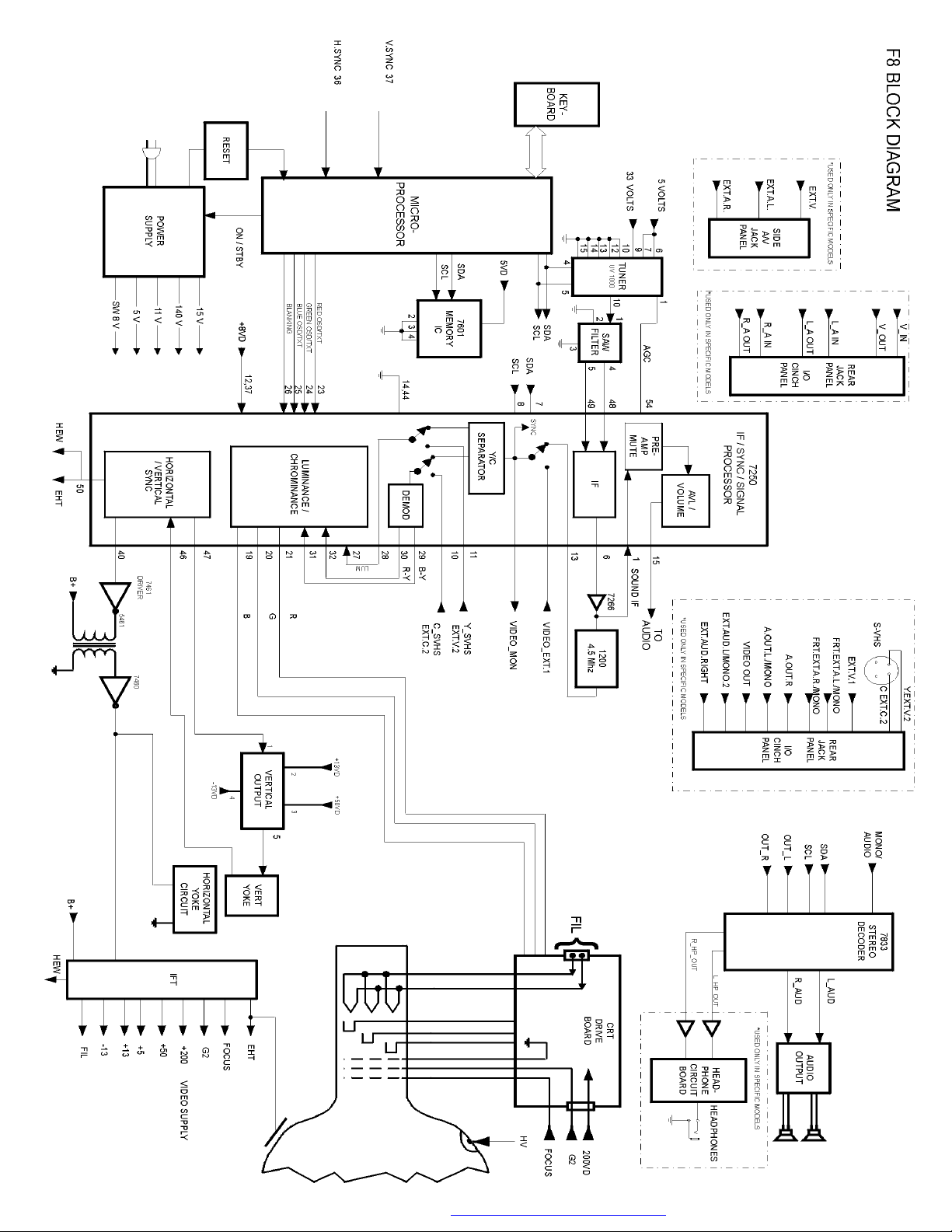
(Display Signal Flow Block Diagram)
PDF created with FinePrint pdfFactory trial version http://www.pdffactory.com
Page 28
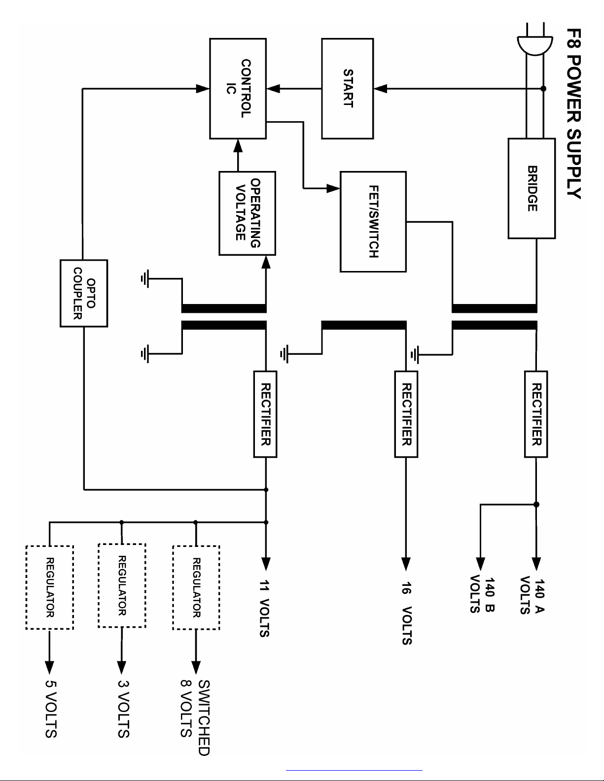
(Display Power Supply Block Diagram)
PDF created with FinePrint pdfFactory trial version http://www.pdffactory.com
Page 29

Philips Consumer Electronics
Technical Service Data
Service Solutions Group
Technical Publications Dept.
P.O. Box 555
401 East Old City Johnson Hwy.
Jefferson City, TN 37760
Manual 7583
Model no.: 25PT10C121
Chassis no.: 25F8
First Publish: 10-9-2000
Rev. Date: 3-21-2001
Print Date: 4/12/2003
Mechanical Assembly
REFER TO SAFETY GUIDELINES
SAFETY NOTICE: ANY PERSON ATTEMPTING TO SERVICE THIS CHASSIS MUST FAMILIARIZE
HIMSELF WITH THE CHASSIS AND BE AWARE OF THE NECESSARY SAFETY PRECAUTIONS
TO BE USED WHEN SERVICING ELECTRONIC EQUIPMENT CONTAINING HIGH VOLTAGES.
CAUTION: USE A SEPARATE ISOLATION TRANSFORMER FOR THIS UNIT WHEN SERVICING
Visit our World Wide Web Site at http://www.magnavox.com
PDF created with FinePrint pdfFactory trial version http://www.pdffactory.com
Page 30

DISASSEMBLY INTRODUCTIONS
(Display Cabinet Back Removal Illustration)
(Display Main Chassis Removal Illustration)
(Display Service Position Illustration)
PDF created with FinePrint pdfFactory trial version http://www.pdffactory.com
Page 31

(Display Cabinet Back Removal Illustration)
PDF created with FinePrint pdfFactory trial version http://www.pdffactory.com
Page 32

(Display Main Chassis Removal Illustration)
PDF created with FinePrint pdfFactory trial version http://www.pdffactory.com
Page 33

(Display Service Position Illustration)
PDF created with FinePrint pdfFactory trial version http://www.pdffactory.com
Page 34

Philips Consumer Electronics
Technical Service Data
Service Solutions Group
Technical Publications Dept.
P.O. Box 555
401 East Old City Johnson Hwy.
Jefferson City, TN 37760
Manual 7583
Model no.: 25PT10C121
Chassis no.: 25F8
First Publish: 10-9-2000
Rev. Date: 3-21-2001
Print Date: 4/12/2003
Mechanical Diagrams
REFER TO SAFETY GUIDELINES
SAFETY NOTICE: ANY PERSON ATTEMPTING TO SERVICE THIS CHASSIS MUST FAMILIARIZE
HIMSELF WITH THE CHASSIS AND BE AWARE OF THE NECESSARY SAFETY PRECAUTIONS
TO BE USED WHEN SERVICING ELECTRONIC EQUIPMENT CONTAINING HIGH VOLTAGES.
CAUTION: USE A SEPARATE ISOLATION TRANSFORMER FOR THIS UNIT WHEN SERVICING
Visit our World Wide Web Site at http://www.magnavox.com
PDF created with FinePrint pdfFactory trial version http://www.pdffactory.com
Page 35

MAIN CABINET EXPLODED VIEW
PDF created with FinePrint pdfFactory trial version http://www.pdffactory.com
Page 36

Philips Consumer Electronics
Technical Service Data
Service Solutions Group
Technical Publications Dept.
P.O. Box 555
401 East Old City Johnson Hwy.
Jefferson City, TN 37760
Manual 7583
Model no.: 25PT10C121
Chassis no.: 25F8
First Publish: 10-9-2000
Rev. Date: 3-21-2001
Print Date: 4/12/2003
Electrical Adjustments
REFER TO SAFETY GUIDELINES
SAFETY NOTICE: ANY PERSON ATTEMPTING TO SERVICE THIS CHASSIS MUST FAMILIARIZE
HIMSELF WITH THE CHASSIS AND BE AWARE OF THE NECESSARY SAFETY PRECAUTIONS
TO BE USED WHEN SERVICING ELECTRONIC EQUIPMENT CONTAINING HIGH VOLTAGES.
CAUTION: USE A SEPARATE ISOLATION TRANSFORMER FOR THIS UNIT WHEN SERVICING
Visit our World Wide Web Site at http://www.magnavox.com
PDF created with FinePrint pdfFactory trial version http://www.pdffactory.com
Page 37

SERVICE ADJUSTMENTS
Required Tools For Servicing:
Isolation Transformer
Multimeter
Oscilloscope
High Voltage (100:1) Oscilloscope Probe
Sencore VG91 Universal Video Generator
Service Adjustment Notes:
Unless Otherwise Specified:
1. All service adjustments are ”hot“ voltagewise. For maximum safety, ensure the
use of properly insulated tools.
2. Refer to the F8 Main Chassis Printed Circuit Board for location of test points and
adjustable components.
3. Grid Locations (Ex.: D-2) next to the reference numbers for components refer to
the Main Chassis Printed Circuit Board.
Caution: The F8 chassis incorporates a ”hot“ ground system. Always use a
separate isolation transformer when applying power to the exposed
chassis.
Focus Adjustment
1. Tune the set to a local or cable station.
2. Adjust the Focus Control (located on the upper part of the flyback transformer) for
best picture details at high light conditions.
Degaussing the Television
1. Position the television so that the screen faces the direction it will be facing when
in use.
2. Ensure the set is turned off.
3. Move a degaussing coil in a circular motion slowly around the sides and front of
the set.
4. Withdraw the degaussing coil at least six feet from the television before
disconnecting it from its power source.
Service Modes:
Introduction
1. There are three service modes used in the F8 chassis. They are:
a. SDM - Service Default Mode
b. SAM - Service Alignment Mode
c. CSM - Customer Service Mode
2. The Service Default Mode (SDM) is a technical aid for the service technician. It is
used for setting of options, reading error codes, and erasing error codes. This
mode displays the Run Timer, Software Version, and current option settings.
Service Default Mode (SDM) also establishes a fixed, repeatable setting of
controls to allow measurements to be made. On screen display is kept at a
minimum to reduce the cluttering of waveforms with unwanted information.
3. The Service Alignment Mode (SAM) is used to make tuning adjustments, align
the white tone, adjust the picture geometry, and make sound adjustments.
4. The Customer Service Mode shows error codes and information on the TV
operation settings. The servicer can instruct the customer to enter CSM by
PDF created with FinePrint pdfFactory trial version http://www.pdffactory.com
Page 38

telephone and read off the information displayed. This helps the servicer to
diagnose problems and failures in the TV set before making a service call.
5. When in a service mode, "SDM" (for Service Default Mode) or ”SAM“ (for Service
Alignment Mode) or ”CSM“ (for Customer Service Mode) will be displayed (in
green) in the top right corner of the screen. All other On Screen Display (except
highlighted items in SDM or SAM) will be in red.
6. It will be memorized in the EEPROM that the TV set is in SDM or SAM. This is
necessary because the TV must show up in SDM or SAM again after an AC
power interrupt.
7. When the television is in SAM or SDM, all normal features (such as volume
control and direct channel access) are available.
EEPROM Replacement or Defective EEPROM
After replacing a EEPROM (or with a defective/no EEPROM) default settings will be
used that enable the set to start up and that allow access to the Service Default Mode
and Service Alignment Mode.
Service unfriendly modes
In the service modes, a number of modes/features are ignored since they interfere
with diagnosing or repairing a set. These are ”service unfriendly modes.“
”Ignoring“ means that the event that is triggered is not executed; the setting remains
unchanged (Example: Timer OFF: 8:00 PM; the set will not switch OFF in service
mode at 8:00PM, but the setting will remain).
The service unfriendly modes are:
• (Sleep) timer
• Blue mute
• Auto switch off (when there is no video signal identified)
• Hotel or hospital mode
• Smart lock or blocking by V-chip
• Skipping and/or blanking of ”Not Favorite“ channels
• Automatic storing of Personal Preset settings
• Automatic user menu time-out (menu switches back or OFF automatically)
Service Default Mode (SDM)
1. The Service Default Mode (SDM), sets the option codes and bytes of the set, and
displays the error codes (the Power LED begins blinking procedure for error code
display, if errors are detected). SDM also overrides software protections.
The Service Default Mode (SDM) must be used when taking voltages and
waveforms.
2. To enter the Service Default Mode, press the following key sequence on the
remote control transmitter:
0-6-2-5-9-6-Menu
Do not allow the display to time out between entries while keying the sequence.
SDM can also be entered by pressing the Channel Down and Volume Down keys
on the local keyboard simultaneously while in SAM mode.
When Service Default Mode is entered, the text "SDM" will be displayed in the
upper right corner of the screen.
3. When Service Default Mode is entered, the Power LED will begin blinking to
display any detected error codes, the set automatically tunes to Channel 3
(61.25 MHz), and service unfriendly modes are disabled. All customer controls
are set to predetermined values.
4. When the unit is operating in Service Default Mode, all normal on-screen displays
are suppressed and replaced by a special service display. A sample SDM display
is shown below.
PDF created with FinePrint pdfFactory trial version http://www.pdffactory.com
Page 39

5. To select an option code or option byte in SDM, use the Menu Up or Menu Down
keys on the remote control.
6. To change the value of an option code, use the Menu Left or Menu Right keys.
7. To change the value of an option byte, enter the new value using the numeric
keys on the remote control.
8. Press the Status button on the remote control to toggle the OSD (except ”SDM“)
ON and OFF to prevent the OSD from interfering with measurements and
oscilloscope waveforms.
9. Press the Menu button on the remote control while in SDM to switch the software
to a Virtual Customer Mode; the text "SDM" will still be displayed in the upper
right corner of the screen. In this mode, all customer menu adjustments to the set
can be made. From the Virtual Customer Mode, press the Menu button to return
to the SDM display.
10. To exit the Service Default Mode and erase the error codes, turn the unit off with
the Power button on the remote control then unplug the AC cord.
11. To exit the Service Default Mode and save the error codes, unplug the AC cord to
turn off the set. When the set is turned on again, the Service Default Mode will
still be active.
Explanation of Display:
Run Timer
The run timer counts the normal operation hours, not the standby hours. The actual
value of the run timer is displayed in SDM and CSM. The run timer displays hours in
hexadecimal format. This display will increment based on the amount of time the
set has been on. The timer will also be incremented one hour each time the set is
turned on.
Software Identification, Cluster, and Version
The software identification, cluster, and version will be shown in the service main
menu display.
These numbers consist of the last part of the customer identification printed on the IC
package; the screen will show ”AAABBC-X.Y“. (Example: L90US11 1.0)
− AAA is the engineering project name (Ex: L90 = L9.0).
− BB is a function specification indicating specific functionality or a region (Ex: US).
Processors with the same engineering project name and function name are
interchangeable, except for the languages they support.
− C is the language cluster number within the ”BB“ software version
PDF created with FinePrint pdfFactory trial version http://www.pdffactory.com
Page 40

(Ex: 11 = English/Spanish/French)
− X is the main version number (Ex: 1)
− Y is the sub version number (Ex: 0)
− the main version number is updated with a major change of specification
(incompatible with the previous software version)
− the sub version number is updated with a minor change (backwards compatible
with the previous versions)
− if the main version number changes, the new version number is written in the
EEPROM
− if the main version number changes, the default settings are loaded
− if the sub version number changes, the new version number is written in the
EEPROM
− if the EEPROM is fresh, the software identification, version and cluster will be
written to EEPROM
− Note: a new micro controller is considered to be compatible if it works instead of
the old software and the functionality is not significantly changed.
Error Buffer
Error codes are required to indicate failures in the television. For intermittent
complaints, always check the error buffer. A unique error code is available for:
• activated protection (error codes 1, 2, and 3)
• failing I2C device
general I2C error
•
• RAM failure (e.g. internal RAM of microprocessor (IC 7600)
Other error codes are:
• Signal processor (IC 7250) start-up error
• EEPROM check-sum error
The last five errors, remembered in the EEPROM, are shown in the service menu.
This is called the error buffer. The error that is found last is displayed on the left,
except when protection (1 to 3) is active. Errors 1, 2, and 3 are often shown at the
right of the error buffer display whenever they are detected.
Example 1:
Suppose the display shows: 8 – 11 – 2– 0 – 0
With 2 displayed at the right of the error buffer, high beam current protection is active.
Example 2:
Suppose the display shows: 11 – 4 – 5– 3 – 0
With 3 displayed at the right of the error buffer, vertical protection is active.
The following error codes have been defined:
Error Code Table:
0 = No error
1 = X-Ray / overvoltage protection active
2 = High beam current (BCI) protection active
3 = Vertical protection active
4 = I²C error while communicating with the sound processor (IC 7833)
5 = Signal processor (IC 7250) start-up error
6 = I²C error while communicating with the signal processor IC (IC 7250)
7 = General I²C error *
8 = Internal RAM error micro controller
9 = EEPROM Configuration error (Checksum error)
PDF created with FinePrint pdfFactory trial version http://www.pdffactory.com
Page 41

10 = I²C error, EEPROM error
11 = I²C error, PLL tuner
Note: I²C = (SCL/SDA)
* General I²C error means: no I²C device is responding to the particular I²C
bus. Possible causes: SCL short circuit to GND, SDA short circuit to GND,
SCL short circuit to SDA, SDA open circuit (at IC 7600), SCL open circuit
(at IC 7600)
Reading Error Codes
Error codes are displayed in the following ways:
1. By SDM display or CSM display
2. By blinking Power LED
1. If the on screen display is working, enter SDM or CSM and read the error buffer
display.
2. If the on screen display is not working, do the following:
a. Remove AC power
b. Use a jumper to connect pin M24 to pin M25 at IC 7601 (D-3)
c. Apply AC power; read the error codes (see LED Sequence List below)
d. If there is no LED indication, take the following steps as needed:
Power on
Press 0–6–2–5–9–6–Menu on the remote control
Note: Some indications take 30 seconds or longer to appear on the LED.
3. LED Sequence List:
a. Wait for long LED on (1.5 seconds)
b. Count the following on flashes (individual errors are separated by 1.5
seconds LED off)
Example:
4. Displayed error codes are saved by removing the AC power. Displayed error
codes are erased by pressing the power button on the remote control or local
keyboard.
PDF created with FinePrint pdfFactory trial version http://www.pdffactory.com
Page 42

Option Code and Status Table
The following options in SDM can be identified:
Note: All options may not be available in some sets.
OPTION OP VALUES
System SY SS (This option is not used in US models)
Option Byte 1
Option Byte 2
Option Byte 3
Option Byte 4
Option Byte 5
Option Byte 6
Option Byte 7
Slider Bar Value Display DP OFF/ON
Animated Menu AM OFF/ON
Hospital Mode HS OFF/ON
Hotel Mode HT OFF/ON
Demo Mode DM OFF/ON
Games Mode GM OFF/ON
Clock (Volatile) CK OFF/ON
Child Lock CL OFF/ON
V-Chip VC OFF/ON
V-Chip Block Unrated VU OFF/ON
Block No Rating (V-Chip) VN OFF/ON
Smart Sound SS OFF/ON
Smart Picture SP OFF/ON
Remote Control Type RC OFF = RC0702/04 remote control / ON =
Channel Select Time Window TW OFF = 2-second time window / ON =
Surf SF OFF/ON
Video Mute (Channel Change) VM OFF/ON
Tuner Type TN OFF = Philips tuner / ON= ALPS tuner
Fine Tuning FT OFF/ON
AV1 XT OFF/ON
AV2 2X OFF/ON
Auto Cable Detect CD OFF/ON
Blue Mute BM OFF/ON
No Ident (Auto Standby) NI OFF/ON
Noise Reduction NR OFF/ON
Contrast Plus CP OFF/ON
Color Temperature CT OFF/ON
East-West Functions EW OFF/ON (This option is not used in US models)
Video Processor Standby BS OFF/ON
Video Processor Auto Startup AS OFF/ON
Bass/Treble Control/Boost BT OFF/ON
Incredible Surround IS OFF/ON
Volume Limiter VL OFF/ON
Ultra Bass UB OFF/ON
Automatic Volume Leveller
(AVL)
SAP - Mono/Stereo DU OFF/ON
Audio Out (Fixed/Variable) AO OFF/ON
Sound Type ST BG/I/DK/M (Should remain on M)
Sound Board SB DB = DBX/SAP (BTSC)
OB1
Option Bytes 1 through 7 are used to set 8 options
OB2
simultaneously with one byte (value can be keyed in
OB3
with numerical buttons on remote control when the
OB4
byte is highlighted).
OB5
Values = 0 – 255
OB6
See the Chassis Feature Listing to see the values for
OB7
Option Bytes 1 through 7. These values can be used
to set the option package for a particular model.
All other remote controls
5-second time window
LV OFF/ON
PDF created with FinePrint pdfFactory trial version http://www.pdffactory.com
Page 43

Sound Board SB DB = DBX/SAP (BTSC)
EC = BTSC stereo (No SAP)
MA = Mono All
MS = Bi Sonic (Mono by tuner, stereo by A/V jacks)
Option SY : System
Function: Set the multi system hardware configuration
Values: SS (This option is not used in US models)
OB 1 – OB 7 : Option Byte 1 – Option Byte 7
Function: Set 8 options simultaneously with one byte
(value can be keyed in with numerical buttons on remote control)
Values: 0 – 255
Option DP : Slider Bar Value Display
Function: Enable/disable slider bar value display in customer menu
Values: OFF = Disable slider bar value display
ON = Enable slider bar value display
Option AM : Animated Menu
Function: Enable/disable animated menu
Values: OFF = Disable animated menu display
ON = Enable animated menu display
Option HS : Hospital Mode
Function: Enable/disable the possibility to enter hospital mode
Values: OFF = Disabled, hospital mode cannot be entered
ON = Enabled, hospital mode can be entered
Option HT : Hotel Mode
Function: Enable/disable the possibility to enter hotel mode
Values: OFF = Disabled, hotel mode cannot be entered
ON = Enabled, hotel mode can be entered
Option DM : Demo Mode
Function: Enable/disable the possibility to enter demo mode
Values: OFF = Disabled, demo mode is not active
ON = Enabled, demo mode is active
Option GM : Games Mode
Function: Enable/disable games function
Values: OFF = Disabled, games command is ignored
ON = Enabled, games command is processed
Option CK : Clock (Volatile)
Function: Enable/disable clock function
Values: OFF = Disabled, clock menu not available
ON = Enabled, clock menu available
Option CL : Child Lock
Function: Enable/disable child lock function
Values: OFF = Disabled, child lock menu not available
ON = Enabled, child lock menu available
Option VC : V-Chip
Function: Enable/disable v-chip function (customer menu item Smartlock)
Values: OFF = Disabled, v-chip menu (customer menu item Smartlock)
Not available
ON = Enabled, v-chip menu (customer menu item Smartlock)
available
Option VU : V-Chip Block Unrated
Function: Enable/disable V-Chip block unrated (in Smartlock menu)
Values: OFF = Disabled, V-Chip block unrated (in Smartlock menu) not
available
ON = Enabled, V-Chip block unrated (in Smartlock menu) available
Option VN : Block No Rating (V-Chip)
Function: Enable/disable block no rating V-Chip (in Smartlock menu)
PDF created with FinePrint pdfFactory trial version http://www.pdffactory.com
Page 44

available
ON = Enabled, block no rating V-Chip (in Smartlock menu) available
Option SS : Smart Sound
Function: Enable/disable smart sound function
Values: OFF = Disabled, Smart Sound command is ignored
ON = Enabled, Smart Sound command is processed
Option SP : Smart Picture
Function: Enable/disable smart picture function
Values: OFF = Disabled, Smart Picture command is ignored
ON = Enabled, Smart Picture command is processed
Option RC : Remote Control Type
Function: Choose the type of remote control to be used
Values: OFF = RC0702/04 remote control
ON = All other remote controls
Note: If changed, this option can only be returned to the original setting by option
byte correction.
Option TW : Channel Select Time Window
Function: Select time window for channel selection
Values: OFF = 2-second time window for channel selection
ON = 5-second time window for channel selection
Option SF : Surf
Function: Enable/disable the possibility to enter surf mode
Values: OFF = Disabled, customer menu item Surf not available and A/CH
command alternates channels
ON = Enabled, customer menu item Surf available and A/CH
command surfs or alternates channels
Option VM : Video Mute (Channel Change)
Function: Enable/disable video mute during channel change
Values: OFF = Disabled, no video mute during channel change
ON = Enabled, video muted during channel change
Option TN : Tuner Type
Function: Choose the tuner type that is configured in the hardware
Values: OFF = Philips tuner (A Philips tuner will have the Philips name
embossed on the side)
ON = ALPS tuner (An ALPS tuner will not have the Philips name
embossed on the side)
Option FT : Fine Tuning
Function: Enable/disable fine tuning
Values: OFF = Customer menu item fine tuning disabled
ON = Customer menu item fine tuning enabled
Option XT : AV1
Function: Enable/disable external input source 1 (Ext 1)
Values: OFF = Disabled, external input source 1 (Ext 1) not available
ON = Enabled, external input source 1 (Ext 1) available
Option 2X : AV2
Function: Enable/disable external input source 2 (Ext 2)
Values: OFF = Disabled, external input source 2 (Ext 2) not available
ON = Enabled, external input source 2 (Ext 2) available
Option CD : Auto Cable Detect
Function: Enable/disable automatic detection of Cable/Broadcast during autostore.
Values: OFF = Disabled, autostore uses the selected Cable/Broadcast setting
ON = Enabled, autostore will detect and set Cable/Broadcast mode
Option BM : Blue Mute
Function: Enable/disable blue mute when no television station signal is present
PDF created with FinePrint pdfFactory trial version http://www.pdffactory.com
Page 45

Values: OFF = Disabled, no blue mute when no television station signal is present
ON = Enabled, blue mute active when no television station signal is
present
Option NI : No Ident (Auto Standby)
Function: Enable/disable automatic switch to standby after 10 minutes when no
television station signal is present
Values: OFF = Disabled, no automatic switch to standby
ON = Enabled, set switches to standby after 10 minutes when no
television station signal is present
Option NR : Noise Reduction
Function: Enable/disable noise reduction function
Values: OFF = Disabled, customer menu item Noise Reduction not available
ON = Enabled, customer menu item Noise Reduction available
Option CP : Contrast Plus
Function: Enable/disable contrast plus function
Values: OFF = Disabled, customer menu item Contrast Plus not available
ON = Enabled, customer menu item Contrast Plus available
Option CT : Color Temperature
Function: Enable/disable color temperature function
Values: OFF = Disabled, customer menu item Color Temperature not available
ON = Enabled, customer menu item Color Temperature available
Option EW : East-West Functions
Function: Enable/disable east-west control function
Values: OFF = Disabled, east-west alignment not available in SAM (EWW,
EWP, EWC, EWT)
ON = Enabled, east-west alignment available in SAM (EWW, EWP, EWC, EWT)
Option BS : Video Processor Standby
Function: Enable/disable video processor standby
Values: OFF = Disabled, video processor standby is not active
ON = Enabled, video processor standby is active
Option AS : Video Processor Auto Startup
Function: Enable/disable video processor auto-startup
Values: OFF = Enabled, video processor is in auto-startup mode
ON = Disabled, video processor is switched on under control of
microcontroller
Option BT : Bass/Treble Control/Boost
Function: Enable/disable bass and treble function
Values: OFF = Disabled, customer menu items Bass and Treble not available
ON = Enabled, customer menu items Bass and Treble available
Option IS : Incredible Surround
Function: Enable/disable incredible surround function
Values: OFF = Disabled, incredible surround function not available
ON = Enabled, incredible surround function available
Option VL : Volume limiter
Function: Enable/disable volume limiter
Values: OFF = Disabled, customer menu item Volume Limiter not available
ON = Enabled, customer menu item Volume Limiter available
Option UB : Ultra Bass
Function: Enable/disable ultra bass function
Values: OFF = Disabled, ultra bass function not available
ON = Enabled, ultra bass function available
Option LV : Automatic Volume Leveller (AVL)
Function: Enable/disable automatic volume leveller function
Values: OFF = Disabled, customer menu item AVL not available
ON = Enabled, customer menu item AVL available
Option DU : SAP
PDF created with FinePrint pdfFactory trial version http://www.pdffactory.com
Page 46

Function: Set SAP configuration (sets with DBX stereo system only)
Values: OFF = Disabled, stereo/SAP not available
ON = Enabled, stereo/SAP available
Option AO : Audio Out (Fixed/Variable)
Function: Set audio output type (where present)
Values: OFF = Fixed audio out
ON = Variable audio out (always on)
Option ST : Sound Type
Function: Set the sound type
Values: BG PAL system
I PAL system
DK PAL system
M Default for USA
Option SB : Sound Board
Function: Set the sound board configuration
Values: DB = DBX/SAP (BTSC)
EC = BTSC stereo (No SAP)
MA = Mono All
MS = BiSonic (Mono from tuner, Stereo from A/V jacks)
Service Alignment Mode (SAM)
1. The Service Alignment Mode (SAM) is used to make tuning adjustments, align
the white tone, adjust the picture geometry, and make sound adjustments.
2. To enter the Service Alignment Mode (SAM), press the following key sequence
on the remote control transmitter:
0-6-2-5-9-6-Status
Do not allow the display to time out between entries while keying the sequence.
SAM can also be entered by pressing the Channel Down and Volume Down keys
on the local keyboard simultaneously while in SDM mode.
When Service Alignment Mode is entered, the text "SAM" will be displayed in the
top right corner of the screen.
3. When Service Alignment Mode is entered, service unfriendly modes are disabled.
The following volatile SAM item values are set:
♦ AKB = 0
♦ VSD = 0
♦ AFW = 275 kHz
♦ SBL = 0
4. When the unit is operating in Service Alignment Mode, all normal on-screen
displays are suppressed and replaced by a special service display. The first
screen seen upon entering SAM is the ”top level SAM menu.“ The service
technician must return to the top level SAM menu before exiting with a power-off
command.
A sample SAM top level menu display is shown below.
PDF created with FinePrint pdfFactory trial version http://www.pdffactory.com
Page 47

Explanation of top level SAM menu display:
The Software Identification, Cluster, and Version are explained in the Service Default
Mode section under ”Explanation of Display.“
The Menu Items and Sub Menus are explained below.
Note: The ”Audio“ sub menu will not be seen on screen when Service Alignment
Mode is first entered. Use the Menu Up and Menu Down buttons on the
remote control to view all menu items and sub menu choices.
5. To select a menu item or a sub menu in SAM, use the Menu Up or Menu Down
keys on the remote control to highlight the item or menu you wish to adjust.
6. To change the value of a highlighted SAM menu item (AKB or VSD), use the
Menu Left or Menu Right keys on the remote control.
7. To enter a highlighted SAM sub menu, use the Menu Left or Menu Right keys.
After entering the sub menu, use the Menu Up or Menu Down to select an item
within the sub menu.
Use the Menu Left or Menu Right keys to change the value of the selected item.
Press the Menu button to return to the top level SAM menu.
8. Press the Menu button on the remote control while in SAM to switch the software
to a Virtual Customer Mode; the text "SAM" will still be displayed in the upper right
corner of the screen. In this mode, all customer menu adjustments to the set can
be made. From the Virtual Customer Mode, press the Menu button to return to
the SAM Menu.
9. Press the Status button on the remote control to toggle the OSD (except ”SAM“)
ON and OFF.
10. To exit the Service Alignment Mode, turn the set off with the Power button on the
remote control. To turn off the set without exiting SAM (or erasing any stored
error codes), unplug the AC cord. When the set is powered on again, the Service
Alignment Mode will still be active.
Note: When SAM is exited or a power interrupt occurs, the volatile SAM items
AKB, VSD, AFW, and SBL will be reset to their original values.
Main Menu
The SAM main menu contains the following items:
− AKB
− VSD
− Tuner sub menu
− White Tone sub menu
− Geometry sub menu
PDF created with FinePrint pdfFactory trial version http://www.pdffactory.com
Page 48

− Audio sub menu
Menu: MAIN Values Remarks
AKB Black current loop
(Auto Kine Bias)
VSD Vertical scan
disable
TUNER
WHITE TONE
GEOMETRY
AUDIO
OFF/ON (0/1)
OFF/ON (0/1)
>
>
>
>
Tuner sub menu
The tuner sub menu contains the following items:
− IF-PLL
− AFW
− AGC
− YD
− CL
− AFA and AFB
The items AFA and AFB cannot be selected; they are for monitoring purposes only.
The item values are stored in EEPROM if this sub menu is left.
A sample display of the Tuner sub menu is shown below.
Sub Menu: TUNER Values Remarks
IF-PLL IF-PLL alignment 0 – 127 This adjustment is auto-aligned
(no action required)
AFW AFC window 125/275
kHz
AGC AGC takeover
point
YD Y-delay 0 – 15 Always set to 12 (no effect)
0 – 63 See below
Always set to 275 kHz
PDF created with FinePrint pdfFactory trial version http://www.pdffactory.com
Page 49

YD Y-delay
adjustment
CL Cathode drive
level
AFA 0 / 1 read only, not accessible
AFB 0 / 1 read only, not accessible
0 – 15 Always set to 12 (no effect)
0 – 7 Always set to 4
Tuner Adjustment:
AGC Takeover Point (AGC):
1. Enter the Service Alignment Mode (SAM) by pressing the following key sequence
on the remote control transmitter:
0-6-2-5-9-6-Status
Do not allow the display to time out between entries while keying the sequence.
2. From the top level SAM menu, use the Menu Up/Down keys to highlight the
Tuner sub menu.
3. Use the menu left/right keys to enter the Tuner sub menu.
4. In the Tuner sub menu, use the Menu Up/Down keys to highlight AGC.
5. Use the Menu Right key to raise the value of AGC until snow appears in the
picture.
6. Then use the Menu Left/Right keys to reduce AGC value until the snow
disappears.
a. AGC values between 10 and 20 are nominal.
b. Single digit AGC values may cause overload.
7. Upon completion of Tuner adjustment, press the Menu button to return to the top
level SAM menu.
White Tone sub menu
The white tone sub menu contains the following items:
− Normal Red
− Normal Green
− Normal Blue
− Delta Cool Red
− Delta Cool Green
− Delta Cool Blue
− Delta Warm Red
− Delta Warm Green
− Delta Warm Blue
Note: Delta values are only used in models with the item ”Color Temperature“ in the
customer menu.
OSD is kept to a minimum in this menu, in order to make white tone alignment
possible.
The item values are stored in EEPROM if this sub menu is left.
The Contrast Plus feature (black stretch) is set to OFF when the White Tone sub
menu is entered.
A sample display of the White Tone sub menu is shown below.
PDF created with FinePrint pdfFactory trial version http://www.pdffactory.com
Page 50

Sub Menu: WHITE TONE Value
Range
NORMAL Starting Values:
NORMAL RED 0 – 63 45
NORMAL GREEN 0 – 63 32
NORMAL BLUE 0 – 63 39
COOL
DELTA COOL RED –2 Delta values are a change of the
DELTA COOL GREEN 0
DELTA COOL BLUE +6
WARM
DELTA WARM RED +2
DELTA WARM GREEN 0
DELTA WARM BLUE –7
White Tone Adjustments:
Note: The following procedure was performed with a Sencore VG91 Universal Video
Generator providing grey scale bars.
1. Enter the Service Alignment Mode (SAM) by pressing the following key sequence
on the remote control transmitter:
0-6-2-5-9-6-Status
Do not allow the display to time out between entries while keying the sequence.
2. From the top level SAM menu, use the Menu Up/Down keys to highlight the
White Tone sub menu.
3. Use the Menu Left/Right keys to enter the White Tone sub menu.
4. Set the VG91 Generator as follows: STD TV Ch. 3, RF-IF Range set to HI, RF-IF
Default
Value
Remarks
normal values. These start at
the default values, and are set to
achieve cool and warm steps of
color temperature in the
customer menu.
Standard factory settings are
given as the default values.
PDF created with FinePrint pdfFactory trial version http://www.pdffactory.com
Page 51

Level set to NORMAL (1), Video Pattern = Raster, R-G-B raster controls OFF.
5. Connect the RF output of the generator to the Television Antenna Input, and
adjust the VG91 level to remove any snow from the raster.
6. Turn off chroma at generator and leave grey scale bars.
7. From the White Tone sub-menu, use the Menu Up/Down keys to select Normal
Red, Normal Green, or Normal Blue. Then use the Menu Left/Right keys to adjust
the values to obtain the best white balance.
8. A reasonable starting point for NORMAL is:
Normal Red=45, Normal Green=32, Normal Blue=39
9. After NORMAL is set, use the same method to set DELTA COOL and DELTA
WARM as offsets.
A reasonable starting point for DELTA COOL is:
Delta Cool Red=(–2), Delta Cool Green=0, Delta Cool Blue=+6
A reasonable starting point for DELTA WARM is:
Delta Warm Red=+2, Delta Warm Green=0, Delta Warm Blue=(-7)
10. After the values are set, or if no changes are required, press Menu to return to
the top level SAM menu.
Geometry sub menu
OSD is kept to a minimum in this sub menu in order to make picture geometry
adjustments possible.
The item values are stored in EEPROM if this sub menu is left.
The value of item Service Blanking (SBL) is not stored in EEPROM, and it is set to
OFF when the geometry sub menu is exited.
A sample display of the Geometry sub menu is shown below.
The picture geometry sub menu contains the following items:
Sub
Menu:
VAM Vertical amplitude 0 – 63
VSL Vertical slope 0 – 63
SBL Service blanking ON/OFF
HSH Horizontal shift 0 – 63
GEOMETRY Values Remarks
PDF created with FinePrint pdfFactory trial version http://www.pdffactory.com
Page 52

EWW E-W width 0 – 63 Only available in models with an
East-West Panel (Diode Modulator)
EWP E-W parabola/width 0 – 63 Only available in models with an
East-West Panel (Diode Modulator)
EWT E-W trapezium 0 – 63 Only available in models with an
East-West Panel (Diode Modulator)
EWC E-W corner parabola 0 – 63 Only available in models with an
East-West Panel (Diode Modulator)
H60 Delta HSH for 60 Hz 0 – 15 Not used
V60 Delta VAM for 60 Hz 0 – 15 Not used
VSC Vertical S-Correction 0 – 63
VSH Vertical shift 0 – 63
Geometry Adjustments:
Notes:
1. The following Geometry adjustments were performed with a Sencore VG91
Universal Video Generator.
2. Set the VG91 Generator as follows: STD TV Ch. 3, RF-IF Range set to HI, RF-IF
Level set to NORMAL (1), Video Pattern = Raster, R-G-B raster controls OFF,
crosshatch or center cross pattern as required.
3. Connect the RF output of the generator to the Television Antenna Input, and
adjust the VG91 level to remove any snow from the raster.
Vertical Shift (VSH):
1. Enter the Service Alignment Mode (SAM) by pressing the following key sequence
on the remote control transmitter:
0-6-2-5-9-6-Status
Do not allow the display to time out between entries while keying the sequence.
2. From the top level SAM menu, use the Menu Up/Down keys to highlight the
Geometry sub menu.
3. Use the Menu Left/Right keys to enter the Geometry sub menu.
4. In the Geometry sub-menu, use the Menu Up/Down keys to select VAM.
5. Input a center cross pattern to the antenna/cable input terminal.
6. Using the Menu Left/Right keys, adjust VSH so that the horizontal bar is properly
centered, top to bottom.
7. If other Geometry adjustments are needed, proceed to the necessary adjustment
using the Menu Up/Down buttons.
8. Upon completion of Geometry adjustments, press the Menu button to return to
the top level SAM menu.
Vertical Amplitude (VAM):
1. Enter the Service Alignment Mode (SAM) by pressing the following key sequence
on the remote control transmitter:
0-6-2-5-9-6-Status
Do not allow the display to time out between entries while keying the sequence.
2. From the top level SAM menu, use the Menu Up/Down keys to highlight the
Geometry sub menu.
3. Use the Menu Left/Right keys to enter the Geometry sub menu.
4. In the Geometry sub-menu, use the Menu Up/Down keys to select VAM.
5. Input a crosshatch pattern to the antenna/cable input terminal.
6. Using the Menu Left button, reduce the value so that the picture does not fill the
entire screen.
PDF created with FinePrint pdfFactory trial version http://www.pdffactory.com
Page 53

7. Use the Menu Up/Down keys to select VSH (Vertical Shift) from the Geometry
sub-menu and, using the Menu Left/Right keys, center the picture on the screen,
top to bottom.
8. Using the cursor up/down keys, select VAM from the Geometry sub-menu, and
use the Menu Right key to increase the value to obtain a slight overscan.
9. If other Geometry adjustments are needed, proceed to the necessary adjustment
using the Menu Up/Down buttons.
10. Upon completion of Geometry adjustments, press the Menu button to return to
the top level SAM menu.
Horizontal Shift (HSH):
Note: This adjustment centers the video on the raster. It does not move the raster.
1. Enter the Service Alignment Mode (SAM) by pressing the following key sequence
on the remote control transmitter:
0-6-2-5-9-6-Status
Do not allow the display to time out between entries while keying the sequence.
2. From the top level SAM menu, use the Menu Up/Down keys to highlight the
Geometry sub menu.
3. Use the Menu Left/Right keys to enter the Geometry sub menu.
4. In the Geometry sub-menu, use the Menu Up/Down keys to select HSH.
5. Input a center cross pattern to the antenna/cable input terminal.
6. Using the Menu Left/Right keys, adjust HSH so that the vertical bar is properly
centered, left to right.
7. If other Geometry adjustments are needed, proceed to the necessary adjustment
using the Menu Up/Down keys.
8. Upon completion of Geometry adjustments, press the Menu button to return to
the top level SAM menu.
Vertical Slope (VSL):
1. Enter the Service Alignment Mode (SAM) by pressing the following key sequence
on the remote control transmitter:
0-6-2-5-9-6-Status
Do not allow the display to time out between entries while keying the sequence.
2. From the top level SAM menu, use the Menu Up/Down keys to highlight the
Geometry sub menu.
3. Use the Menu Left/Right keys to enter the Geometry sub menu.
4. In the Geometry sub-menu, use the Menu Up/Down keys to select VSL.
5. Input a crosshatch pattern to the antenna/cable input terminal.
6. Using the Menu Left/Right keys, adjust VSL so that the squares at the bottom of
the screen are equal in size to the squares at the top of the screen.
7. If other Geometry adjustments are needed, proceed to the necessary adjustment
using the Menu Up/Down keys.
8. Upon completion of Geometry adjustments, press the Menu button to return to
the top level SAM menu.
Vertical S-Correction (VSC):
1. Enter the Service Alignment Mode (SAM) by pressing the following key sequence
on the remote control transmitter:
0-6-2-5-9-6-Status
Do not allow the display to time out between entries while keying the sequence.
2. From the top level SAM menu, use the Menu Up/Down keys to highlight the
Geometry sub menu.
3. Use the Menu Left/Right keys to enter the Geometry sub menu.
4. In the Geometry sub-menu, use the Menu Up/Down keys to select VSC.
PDF created with FinePrint pdfFactory trial version http://www.pdffactory.com
Page 54

5. Input a crosshatch pattern to the antenna/cable input terminal.
6. Using the Menu Left/Right keys, adjust VSC so that the squares at the center of
the screen are equal in size to the squares at the top and bottom of the screen.
7. If other Geometry adjustments are needed, proceed to the necessary adjustment
using the Menu Up/Down keys.
8. Upon completion of Geometry adjustments, press the Menu button to return to
the top level SAM menu.
Service Blanking (SBL):
Service Blanking provides a straight cutoff line in the center of the raster. It is useful
when centering the raster. It can also be used in adjusting the yoke and setting
vertical size and linearity.
1. Enter the Service Alignment Mode (SAM) by pressing the following key sequence
on the remote control transmitter:
0-6-2-5-9-6-Status
Do not allow the display to time out between entries while keying the sequence.
2. From the top level SAM menu, use the Menu Up/Down keys to highlight the
Geometry sub menu.
3. Use the Menu Left/Right keys to enter the Geometry sub menu.
4. In the Geometry sub-menu, use the Menu Up/Down keys to select SBL.
5. Use the Menu Left/Right keys to toggle SBL ON or OFF.
6. With SBL on, VSH can be used to center the raster on the fiduciary marks (the
small notches in the phosphor on the right and left edge of the CRT). These are
absolute center.
7. If other Geometry adjustments are needed, proceed to the necessary adjustment
using the Menu Up/Down keys.
8. Upon completion of Geometry adjustments, press the Menu button to return to
the top level SAM menu.
Delta HSH for 60Hz (H60):
Note: This adjustment should not be changed from the factory preset value (10).
Delta VAM for 60Hz (V60):
Note: This adjustment should not be changed from the factory preset value (5).
Note: The following GEOMETRY adjustments can only be performed on models
containing an East-West Panel (Diode Modulator).
East-West Width (EWW):
1. Enter the Service Alignment Mode (SAM) by pressing the following key sequence
on the remote control transmitter:
0-6-2-5-9-6-Status
Do not allow the display to time out between entries while keying the sequence.
2. From the top level SAM menu, use the Menu Up/Down keys to highlight the
Geometry sub menu.
3. Use the Menu Left/Right keys to enter the Geometry sub menu.
4. In the Geometry sub menu, use the Menu Up/Down keys to select EWW.
5. Input a crosshatch pattern to the antenna/cable input terminal.
6. Use the Menu Left key to reduce the value of EWW so that the picture does not fill
the entire screen.
7. Use the Menu Up/Down keys to select HSH (Horizontal Shift) from the Geometry
sub menu and, using the Menu Left/Right keys, center the picture on the screen.
8. Use the Menu Up/Down keys to select EWW from the Geometry sub menu, and
use the Menu Right key to increase the value to obtain a slight overscan.
PDF created with FinePrint pdfFactory trial version http://www.pdffactory.com
Page 55

Note: Remember, adjusting EWW will affect other horizontal adjustments.
9. If other Geometry adjustments are needed, proceed to the necessary adjustment
using the Menu Up/Down keys.
10. Upon completion of Geometry adjustments, press the Menu button to return to
the top level SAM menu.
East-West Parabola/Width (EWP):
1. Enter the Service Alignment Mode (SAM) by pressing the following key sequence
on the remote control transmitter:
0-6-2-5-9-6-Status
Do not allow the display to time out between entries while keying the sequence.
2. From the top level SAM menu, use the Menu Up/Down keys to highlight the
Geometry sub menu.
3. Use the Menu Left/Right keys to enter the Geometry sub menu.
4. In the Geometry sub menu, use the Menu Up/Down keys to select EWP.
5. Input a crosshatch pattern to the antenna/cable input terminal.
6. Use the Menu Left/Right keys to adjust the value of EWP.
7. This adjusts the top and bottom of the right and left side of the raster, adjusting the
raster by “bending” it out or in.
8. This adjustment should be set so that the screen appears to be straight and “flat.”
9. If other Geometry adjustments are needed, proceed to the necessary adjustment
using the Menu Up/Down keys.
10. Upon completion of Geometry adjustments, press the Menu button to return to
the top level SAM menu.
East-West Trapezium (EWT):
1. Enter the Service Alignment Mode (SAM) by pressing the following key sequence
on the remote control transmitter:
0-6-2-5-9-6-Status
Do not allow the display to time out between entries while keying the sequence.
2. From the top level SAM menu, use the Menu Up/Down keys to highlight the
Geometry sub menu.
3. Use the Menu Left/Right keys to enter the Geometry sub menu.
4. In the Geometry sub menu, use the Menu Up/Down keys to select EWT.
5. Input a crosshatch pattern to the antenna/cable input terminal.
6. Use the Menu Left/Right keys to adjust the value of EWT.
7. This balances the width at the top of the screen to the width at the bottom of the
screen.
8. This adjustment should be set so the top and bottom of the screen are of equal
width.
9. If other Geometry adjustments are needed, proceed to the necessary adjustment
using the Menu Up/Down keys.
10. Upon completion of Geometry adjustments, press the Menu button to return to
the top level SAM menu.
East-West Corner Parabola (EWC):
1. Enter the Service Alignment Mode (SAM) by pressing the following key sequence
on the remote control transmitter:
0-6-2-5-9-6-Status
Do not allow the display to time out between entries while keying the sequence.
2. From the top level SAM menu, use the Menu Up/Down keys to highlight the
Geometry sub menu.
3. Use the Menu Left/Right keys to enter the Geometry sub menu.
4. In the Geometry sub menu, use the Menu Up/Down keys to select EWC.
5. Input a crosshatch pattern to the antenna/cable input terminal.
PDF created with FinePrint pdfFactory trial version http://www.pdffactory.com
Page 56

6. Use the Menu Left/Right keys to adjust the value of EW CORNER.
7. This adjustment affects the very corner sections of the raster, and acts as a
“touch-up” of the EWP (East-West Parabola/Width) adjustment.
8. This adjustment should be set so the corners of the screen are straight and equal
in size.
9. If other Geometry adjustments are needed, proceed to the necessary adjustment
using the Menu Up/Down keys.
10. Upon completion of Geometry adjustments, press the Menu button to return to
the top level SAM menu.
Audio sub menu
The audio sub menu item values are stored in EEPROM if this sub menu is left.
A sample display of the Audio sub menu is shown below.
The Audio sub menu contains the following item on stereo chassis:
Sub Menu: AUDIO Values Remarks
AT Attack time at AVL 1 – 4 Normal setting is
4.
Audio Adjustment:
Attack Time at AVL (AT):
1. Enter the Service Alignment Mode (SAM) by pressing the following key sequence
on the remote control transmitter:
0-6-2-5-9-6-Status
Do not allow the display to time out between entries while keying the sequence.
2. From the top level SAM menu, use the Menu Up/Down keys to highlight the Audio
sub menu.
3. Use the Menu Left/Right keys to enter the Audio sub menu.
4. Use the Menu Left/Right keys to adjust the value of AT.
5. Set the volume of AT to 4.
6. Upon completion of Audio adjustment, press the Menu button to return to the top
level SAM menu.
PDF created with FinePrint pdfFactory trial version http://www.pdffactory.com
Page 57

Convergence and Purity Adjustments
Notes:
1. The following adjustments were performed with a Sencore VG91 Universal Video
Generator.
2. Set the VG91 Generator as follows: STD TV Ch. 3, RF-IF Range set to HI, RF-IF
Level set to NORMAL (1), Video Pattern = Raster, R-G-B raster controls OFF,
Mode Switch set to L+R, Audio Frequency set to 300Hz, and 0 Pilot (max. CCW).
3. Connect the RF output of the generator to the Television Antenna Input, and
adjust the VG91 level to remove any snow from the raster.
Pre-Convergence Procedure
Note: The degaussing procedure should be performed prior to this adjustment.
1. Place the multi-pole Purity and Convergence Assembly with the 2-Y pole purity
rings directly in the gap between the G2 and G3 (focus) grids as shown in the
"Convergence and Purity Assembly" graphic.
2. Enter Service Alignment Mode (refer to Service Alignment Mode section).
3. Apply a center cross or crosshatch pattern to the antenna/cable input terminal.
4. Select the White Tone sub-menu by pressing the Menu Up/Down keys on the
remote control so that White Tone is highlighted.
5. Use the Menu Left/Right keys to enter the White Tone sub-menu.
6. Use Menu Up/Down keys to toggle between the options. Be sure to record the
values of all options (Normal Red/Green/Blue, Delta Cool Red/Green/Blue, and
Delta Warm Red/Green/Blue).
7. Use the Menu Up/Down keys to select Normal Green, and use the Menu Left key
to set Normal Green to minimum.
8. Loosen the yoke clamp screw, pull the yoke back, and remove the three yoke
wedges.
9. Slide the yoke all the way forward so that it rests against the bell of the CRT.
10 Tighten the yoke clamp screw so that the yoke does not drop away from the bell
of the CRT.
11. Slowly spread, and if necessary, rotate the 2-Y pole purity rings so that the red
and blue lines are at least parallel and preferably coincide at the 6:00 and 12:00
positions as shown in the "2Y Spread and 2Y Rotate" graphic.
12. Proceed to the Color Purity Adjustment.
Color Purity Adjustment
1. Connect a solid white pattern signal to the antenna/cable input terminal.
2. Use the Menu Up/Down keys to select Normal Blue, and use the Menu Left key to
set Normal Blue to minimum.
3. Use the Menu Up/Down keys to select Normal Red, and use the Menu Right key
to set Normal Red to maximum.
4. Slowly spread the 2-X pole purity rings to center the red portion of the screen,
leaving the same amount of green on one side of the screen as blue on the other
side.
5. Tighten the yoke clamp screw slightly so that the yoke may be moved with some
friction.
6. Proceed to the Static Center Convergence Adjustment.
Static Center Convergence Adjustment
1. Apply a center cross or crosshatch pattern to the antenna/cable input terminal
and observe the screen to ensure that the yoke is not tilted. If necessary, rotate
PDF created with FinePrint pdfFactory trial version http://www.pdffactory.com
Page 58

the yoke to obtain a level raster.
2. Use the Menu Up/Down keys to select Normal Blue, and use the Menu Right key
to set Normal Blue to maximum.
3. Slowly spread, and if necessary, rotate the 4-pole magnetic rings to converge red
and blue lines at the center of the screen.
4. Use the Menu Up/Down keys to select Normal Green, and use the Menu Right
key to set Normal Green to maximum.
5. Slowly spread, and if necessary, rotate the 6-pole magnetic rings to converge
red/blue on green lines at the center of the screen.
6. Repeat steps three and five for optimum performance.
7. Proceed to the Dynamic Edge Convergence Adjustment.
(Display Convergence and Purity Assembly)
Dynamic Edge Convergence Adjustment
Note: To secure the correct position of the deflection yoke, three rubber wedges are
used. They are ultimately to be placed as shown in Figure 3c or Figure 4c.
1. Apply a crosshatch pattern to the antenna/cable input terminal.
2. Use the Menu Up/Down keys to select Normal Green, and use the Menu Left key
to set Normal Green to minimum.
3. Tilt the yoke up and down to converge the red and blue vertical lines at the 6:00
and 12:00 positions and the red and blue horizontal lines at the 3:00 and 9:00
positions (refer to Figure 5 ). When the correct position has been found, place a
rubber wedge between the yoke and the CRT. If the yoke is tilted up, place
wedge one as shown in Figure 3a; if it is tilted down, place wedge one as shown
in Figure 4a.
4. Tilt the yoke to the left and right to find the point of best possible convergence of
the red and blue lines at the edges, top and bottom of the screen as shown in
Figure 6. When the correct position is located, place wedges two and three as
shown in Figure 3b or Figure 4b.
5. Remove wedge one and place it in the final position as shown in Figure 3c or
Figure 4c.
6. Use the Menu Up/Down keys to select Normal Green, and use the Menu Right
key to set Normal Green to maximum.
7. Proceed to the White Balance Setup.
(Display Figures 3a, 3b, 3c, 4a, 4b, & 4c of Wedge Placement
Display)
(Display Figures 5 & 6 of Yoke Tilt Display)
Master Screen (VG2)/ White Balance Setup:
1. With the set OFF, rotate VG2 (located on the lower part of the flyback
transformer) counterclockwise.
2. Use the Power Button (on the remote control or the local keyboard) to turn the set
ON, without a signal, and rotate VG2 clockwise until snow is visible.
3. Enter Service Alignment Mode (refer to Service Alignment Mode section).
4. Enter the Virtual Customer Menu by pressing the Menu button on the remote and
set brightness and picture to 31 and color to 0.
5. Apply an NTSC color bar signal to the antenna/cable input terminal and tune to
the active channel.
9. Connect an oscilloscope, 20V per division and 10 uSec time base, at the junction
of resistors 3333 and 3334 on the CRT Board. Observe the stairstep pattern
PDF created with FinePrint pdfFactory trial version http://www.pdffactory.com
Page 59

while adjusting VG2.
Hint: Counterclockwise adjustment will compress bottom of stairstep pattern.
Clockwise adjustment will compress top of stairstep pattern.
10. Adjust VG2 midway between top and bottom compression.
11. Proceed to White-Tone Adjustments under White Tone sub-menu in the Service
Alignment Mode section to complete White Balance Setup.
Customer Service Mode (CSM)
1. The Customer Service Mode (CSM) is used to retrieve data on the TV operation
settings and stored error codes.
2. To enter the Customer Service Mode, press and hold the Mute button on the
remote control and any key on the local keyboard (except ”Power“) for more than 4
seconds. When the set is in Customer Service Mode, the text "CSM" is displayed
in the top right corner of the screen.
3. To use this system, the customer is instructed by phone to enter CSM and read off
the display that appears. This information is useful to gain insights into failures
before traveling to the customer's home.
4. This information can also be used to avoid nuisance trips to the home when the
problem is an operational error (example: Closed Caption is on or set is in Hospital
Mode).
5. When entering CSM, all disruptive functions are turned off, and service unfriendly
modes are ignored. While CSM is active, no changes can be made in settings or
functions. When CSM is exited, the TV returns to all prior operational settings.
6. To exit CSM, press any key (on the remote control or local keyboard) except
”Channel Up“ or ”Channel Down.“
To exit CSM and return the set to normal operation mode, press any key on the
local keyboard or the remote control except Channel Up, Channel Down, or
Power.
To exit CSM and turn the set off, press the Power button on either the TV set or
the remote control.
7. A sample CSM display is shown below.
1 002A L90US11 1.0
2 CODES 0 0 0 0 0
3 OP 202 255 135 228 59 206 208
4 SYS:
5 NOT TUNED
6
7
8
9 VOL LIM 255
C S M
PDF created with FinePrint pdfFactory trial version http://www.pdffactory.com
Page 60

Explanation of CSM Display Screen
The following information is displayed on screen:
• Text ”CSM“ on the first line
• Line number for every line (to make CSM language independent)
• To view multiple CSM pages (such as lines 8 and 9), use the Channel Up or
Channel Down keys
• For more information on lines 1, 2, and 3, see SDM section ”Explanation of
Display“
• Line 1 displays the run timer and the software identification, cluster, and version
• Line 2 displays the error buffer contents (the word ”error“ is not used on this
screen, instead ”codes“ is used)
• Line 3 displays the option code information
• Line 4 displays SYS: (This is not used)
• Lines 5 through 8 display information on active service unfriendly modes
• Line 5 displays the text ”NOT TUNED“ if no television station is tuned
• Line 6 displays the text ”TIMER“ if the sleep timer or ”on“ timer is active
• Line 7 displays the text ”LOCKED“ if one or more channels or presets is locked via
child lock
• Line 8 displays the text ”HOSPITAL“ if hospital mode is active, or ”HOTEL“ if hotel
mode is active
• If the volume limiter is active, line 9 displays the text ”VOL LIM“ and the set value
of the volume limiter. If the volume limiter is inactive, the displayed value will be
255 (the maximum volume allowed).
PDF created with FinePrint pdfFactory trial version http://www.pdffactory.com
Page 61

CSM Flow Chart
any key on the local keyboard
feature settings (that were
when the set is switched on,
picture, sound and feature
Normal operation mode
Press "MUTE" button (RC) and
(except "POWER") for more than 4 seconds
Store current picture, sound and
feature settings (for later retrieval)
Set pre-defined picture, sound and
feature settings
Ignore service unfriendly options
Display CSM information screen
"Channel up"
(RC or local
keyboard)
Exit CSM
Restore picture, sound and
stored during entry)
Other key
"Channel down"
(RC or local
keyboard)
“POWER”
(RC or local
keyboard)
F8 CHASSIS FEATURE LISTINGS
USA/CANADIAN CHASSIS LISTINGS
LATIN AMERICAN CHASSIS LISTINGS
To next CSM pageTo previous CSM page
Off (Exit CSM):
settings (that were stored
during entry) are restored
INDUSTRIAL CHASSIS LISTINGS
PDF created with FinePrint pdfFactory trial version http://www.pdffactory.com
Page 62

Convergence and Purity Assembly - (Display Convergence and Purity Assembly)
PDF created with FinePrint pdfFactory trial version http://www.pdffactory.com
Page 63

2Y Spread and 2Y Rotate
PDF created with FinePrint pdfFactory trial version http://www.pdffactory.com
Page 64

(Display Figures 3a, 3b, 3c, 4a, 4b, & 4c of Wedge Placement Display)
PDF created with FinePrint pdfFactory trial version http://www.pdffactory.com
Page 65

(Display Figures 5 & 6 of Yoke Tilt Display)
PDF created with FinePrint pdfFactory trial version http://www.pdffactory.com
Page 66

USA/CANADIAN CHASSIS LISTINGS
PDF created with FinePrint pdfFactory trial version http://www.pdffactory.com
Page 67

Philips Consumer Electronics
Technical Service Data
Service Solutions Group
Technical Publications Dept.
P.O. Box 555
401 East Old City Johnson Hwy.
Jefferson City, TN 37760
SCHEMATIC DIAGRAMS AND PC BOARDS
1. POWER SUPPLY - SECT. A1 SCHEMATIC
2. HORIZONTAL DEFLECTION - SECT. A2 SCHEMATIC
3. VERTICAL DEFLECTION - SECT. A3 SCHEMATIC
4. SYNCRONIZATION - SECT. A4 SCHEMATIC
5. TUNER/VIDEO IF - SECT. A5 SCHEMATIC
6. VIDEO PROCESSING - SECT. A6 SCHEMATIC
7. CONTROL PROCESSOR - SECT. A7 SCHEMATIC
8. CUSTOME CONTROL - SECT. A8 SCHEMATIC
9. BTSC DECODER - SECT. A9 SCHEMATIC
10. NICAM-2CS DECODER - SECT. A10 SCHEMATIC
11. SMART SOUND - SECT. A11 SCHEMATIC
12. AUDIO AMPLIFIER - SECT. A12 SCHEMATIC
13. HEADPHONE - SECT. A13 SCHEMATIC
14. REAR I/O CINCH - SECT. A14 SCHEMATIC
15. CRT PANEL - SECT. B SCHEMATIC
16. BLOCK DIAGRAM
17. MAIN CHASSIC & CRT PCB (TOP VIEW)
18. MAIN CHASSIS & CRT PCB (BOTTOM VIEW)
Manual 7583
Model no.: 25PT10C121
Chassis no.: 25F8
First Publish: 10-9-2000
Rev. Date: 3-21-2001
Print Date: 4/12/2003
REFER TO SAFETY GUIDELINES
SAFETY NOTICE: ANY PERSON ATTEMPTING TO SERVICE THIS CHASSIS MUST FAMILIARIZE
HIMSELF WITH THE CHASSIS AND BE AWARE OF THE NECESSARY SAFETY PRECAUTIONS
TO BE USED WHEN SERVICING ELECTRONIC EQUIPMENT CONTAINING HIGH VOLTAGES.
CAUTION: USE A SEPARATE ISOLATION TRANSFORMER FOR THIS UNIT WHEN SERVICING
Visit our World Wide Web Site at http://www.magnavox.com
PDF created with FinePrint pdfFactory trial version http://www.pdffactory.com
Page 68

25PT10C121 - Manual# 7583 POWER SUPPLY - SECT. A1 SCHEMATIC Page: 1 of 1825PT10C121 - Manual# 7583 POWER SUPPLY - SECT. A1 SCHEMATIC Page: 1 of 18
PDF created with FinePrint pdfFactory trial version http://www.pdffactory.com
Page 69

25PT10C121 - Manual# 7583 Page: 2 of 18
25PT10C121 - Manual# 7583 Page: 2 of 18
HORIZONTAL DEFLECTION - SECT. A2 SCHEMATIC
HORIZONTAL DEFLECTION - SECT. A2 SCHEMATIC
PDF created with FinePrint pdfFactory trial version http://www.pdffactory.com
Page 70

25PT10C121 - Manual# 7583 VERTICAL DEFLECTION - SECT. A3 SCHEMATICPage: 3 of 1825PT10C121 - Manual# 7583 VERTICAL DEFLECTION - SECT. A3 SCHEMATICPage: 3 of 18
PDF created with FinePrint pdfFactory trial version http://www.pdffactory.com
Page 71

25PT10C121 - Manual# 7583 SYNCRONIZATION - SECT. A4 SCHEMATIC Page: 4 of 1825PT10C121 - Manual# 7583 SYNCRONIZATION - SECT. A4 SCHEMATIC Page: 4 of 18
PDF created with FinePrint pdfFactory trial version http://www.pdffactory.com
Page 72

25PT10C121 - Manual# 7583 TUNER/VIDEO IF - SECT. A5 SCHEMATIC Page: 5 of 1825PT10C121 - Manual# 7583 TUNER/VIDEO IF - SECT. A5 SCHEMATIC Page: 5 of 18
PDF created with FinePrint pdfFactory trial version http://www.pdffactory.com
Page 73

25PT10C121 - Manual# 7583 VIDEO PROCESSING - SECT. A6 SCHEMATIC Page: 6 of 1825PT10C121 - Manual# 7583 VIDEO PROCESSING - SECT. A6 SCHEMATIC Page: 6 of 18
PDF created with FinePrint pdfFactory trial version http://www.pdffactory.com
Page 74

25PT10C121 - Manual# 7583 CONTROL PROCESSOR - SECT. A7 SCHEMATIC Page: 7 of 1825PT10C121 - Manual# 7583 CONTROL PROCESSOR - SECT. A7 SCHEMATIC Page: 7 of 18
PDF created with FinePrint pdfFactory trial version http://www.pdffactory.com
Page 75

25PT10C121 - Manual# 7583 CUSTOME CONTROL - SECT. A8 SCHEMATIC Page: 8 of 1825PT10C121 - Manual# 7583 CUSTOME CONTROL - SECT. A8 SCHEMATIC Page: 8 of 18
PDF created with FinePrint pdfFactory trial version http://www.pdffactory.com
Page 76

25PT10C121 - Manual# 7583 BTSC DECODER - SECT. A9 SCHEMATIC Page: 9 of 1825PT10C121 - Manual# 7583 BTSC DECODER - SECT. A9 SCHEMATIC Page: 9 of 18
PDF created with FinePrint pdfFactory trial version http://www.pdffactory.com
Page 77

25PT10C121 - Manual# 7583 NICAM-2CS DECODER - SECT. A10 SCHEMATIC Page: 10 of 1825PT10C121 - Manual# 7583 NICAM-2CS DECODER - SECT. A10 SCHEMATIC Page: 10 of 18
PDF created with FinePrint pdfFactory trial version http://www.pdffactory.com
Page 78

25PT10C121 - Manual# 7583 SMART SOUND - SECT. A11 SCHEMATIC Page: 11 of 1825PT10C121 - Manual# 7583 SMART SOUND - SECT. A11 SCHEMATIC Page: 11 of 18
PDF created with FinePrint pdfFactory trial version http://www.pdffactory.com
Page 79

25PT10C121 - Manual# 7583 AUDIO AMPLIFIER - SECT. A12 SCHEMATIC Page: 12 of 1825PT10C121 - Manual# 7583 AUDIO AMPLIFIER - SECT. A12 SCHEMATIC Page: 12 of 18
PDF created with FinePrint pdfFactory trial version http://www.pdffactory.com
Page 80

25PT10C121 - Manual# 7583 HEADPHONE - SECT. A13 SCHEMATIC Page: 13 of 1825PT10C121 - Manual# 7583 HEADPHONE - SECT. A13 SCHEMATIC Page: 13 of 18
PDF created with FinePrint pdfFactory trial version http://www.pdffactory.com
Page 81

25PT10C121 - Manual# 7583 REAR I/O CINCH - SECT. A14 SCHEMATIC Page: 14 of 1825PT10C121 - Manual# 7583 REAR I/O CINCH - SECT. A14 SCHEMATIC Page: 14 of 18
PDF created with FinePrint pdfFactory trial version http://www.pdffactory.com
Page 82

25PT10C121 - Manual# 7583 CRT PANEL - SECT. B SCHEMATIC Page: 15 of 1825PT10C121 - Manual# 7583 CRT PANEL - SECT. B SCHEMATIC Page: 15 of 18
PDF created with FinePrint pdfFactory trial version http://www.pdffactory.com
Page 83

25PT10C121 - Manual# 7583 BLOCK DIAGRAM Page: 16 of 1825PT10C121 - Manual# 7583 BLOCK DIAGRAM Page: 16 of 18
PDF created with FinePrint pdfFactory trial version http://www.pdffactory.com
Page 84

25PT10C121 - Manual# 7583 MAIN CHASSIC & CRT PCB (TOP VIEW) Page: 17 of 1825PT10C121 - Manual# 7583 MAIN CHASSIC & CRT PCB (TOP VIEW) Page: 17 of 18
PDF created with FinePrint pdfFactory trial version http://www.pdffactory.com
Page 85

25PT10C121 - Manual# 7583 MAIN CHASSIS & CRT PCB (BOTTOM VIEW) Page: 18 of 1825PT10C121 - Manual# 7583 MAIN CHASSIS & CRT PCB (BOTTOM VIEW) Page: 18 of 18
PDF created with FinePrint pdfFactory trial version http://www.pdffactory.com
Page 86

Philips Consumer Electronics
Technical Service Data
Service Solutions Group
Technical Publications Dept.
P.O. Box 555
401 East Old City Johnson Hwy.
Jefferson City, TN 37760
Manual 7583
Model no.: 25PT10C121
Chassis no.: 25F8
First Publish: 10-9-2000
Rev. Date: 3-21-2001
Print Date: 4/12/2003
Scope Patterns
REFER TO SAFETY GUIDELINES
SAFETY NOTICE: ANY PERSON ATTEMPTING TO SERVICE THIS CHASSIS MUST FAMILIARIZE
HIMSELF WITH THE CHASSIS AND BE AWARE OF THE NECESSARY SAFETY PRECAUTIONS
TO BE USED WHEN SERVICING ELECTRONIC EQUIPMENT CONTAINING HIGH VOLTAGES.
CAUTION: USE A SEPARATE ISOLATION TRANSFORMER FOR THIS UNIT WHEN SERVICING
Visit our World Wide Web Site at http://www.magnavox.com
PDF created with FinePrint pdfFactory trial version http://www.pdffactory.com
Page 87

25PT10C121 - Manual no. 7583 Page: 1 of 3
P4
³
³
³
L4
³
³
³
F2
³
³
³
S1
³
³
³
V2a
³
³
³
P1 P2 P3
L1 L2 L3
L5 L6 F1
F3 L1 F2
V1a V1b V1c
PDF created with FinePrint pdfFactory trial version http://www.pdffactory.com
Page 88

25PT10C121 - Manual no. 7583 continued Page: 2 of 3
V5a
³
³
³
C2
³
³
³
C6
³
³
³
A1a
³
³
³
A2d
³
³
³
V2b V2c V3
V5b V5c C1
C3 C4 C5
A1a A2a A2b
A2a A2b A2c
PDF created with FinePrint pdfFactory trial version http://www.pdffactory.com
Page 89

25PT10C121 - Manual no. 7583 continued Page: 3 of 3
A3d
³
³
³
V6a
³
³
³
2
³
³
³
6
³
³
³
A3a A3b A3c
V4a V4b V4c
V6b V6c 1
3 4 5
7
PDF created with FinePrint pdfFactory trial version http://www.pdffactory.com
Page 90

PDF created with FinePrint pdfFactory trial version http://www.pdffactory.com
Page 91

Philips Consumer Electronics
Technical Service Data
Service Solutions Group
Technical Publications Dept.
P.O. Box 555
401 East Old City Johnson Hwy.
Jefferson City, TN 37760
Manual 7583
Model no.: 25PT10C121
Chassis no.: 25F8
First Publish: 10-9-2000
Rev. Date: 3-21-2001
Print Date: 4/12/2003
Troubleshooting
REFER TO SAFETY GUIDELINES
SAFETY NOTICE: ANY PERSON ATTEMPTING TO SERVICE THIS CHASSIS MUST FAMILIARIZE
HIMSELF WITH THE CHASSIS AND BE AWARE OF THE NECESSARY SAFETY PRECAUTIONS
TO BE USED WHEN SERVICING ELECTRONIC EQUIPMENT CONTAINING HIGH VOLTAGES.
CAUTION: USE A SEPARATE ISOLATION TRANSFORMER FOR THIS UNIT WHEN SERVICING
Visit our World Wide Web Site at http://www.magnavox.com
PDF created with FinePrint pdfFactory trial version http://www.pdffactory.com
Page 92

PDF created with FinePrint pdfFactory trial version http://www.pdffactory.com
Page 93

PDF created with FinePrint pdfFactory trial version http://www.pdffactory.com
Page 94

PDF created with FinePrint pdfFactory trial version http://www.pdffactory.com
Page 95

PDF created with FinePrint pdfFactory trial version http://www.pdffactory.com
Page 96

PDF created with FinePrint pdfFactory trial version http://www.pdffactory.com
Page 97

PDF created with FinePrint pdfFactory trial version http://www.pdffactory.com
Page 98

Philips Consumer Electronics
Technical Service Data
Service Solutions Group
Technical Publications Dept.
P.O. Box 555
401 East Old City Johnson Hwy.
Jefferson City, TN 37760
Manual 7583
Model no.: 25PT10C121
Chassis no.: 25F8
First Publish: 10-9-2000
Rev. Date: 3-21-2001
Print Date: 4/12/2003
Important Information
REFER TO SAFETY GUIDELINES
SAFETY NOTICE: ANY PERSON ATTEMPTING TO SERVICE THIS CHASSIS MUST FAMILIARIZE
HIMSELF WITH THE CHASSIS AND BE AWARE OF THE NECESSARY SAFETY PRECAUTIONS
TO BE USED WHEN SERVICING ELECTRONIC EQUIPMENT CONTAINING HIGH VOLTAGES.
CAUTION: USE A SEPARATE ISOLATION TRANSFORMER FOR THIS UNIT WHEN SERVICING
Visit our World Wide Web Site at http://www.magnavox.com
PDF created with FinePrint pdfFactory trial version http://www.pdffactory.com
Page 99

PDF created with FinePrint pdfFactory trial version http://www.pdffactory.com
Page 100

PDF created with FinePrint pdfFactory trial version http://www.pdffactory.com
 Loading...