

Philips 241B4PYCB/01, 241B4PYCS/01, 241B4PYCB/27, 241B4PYCB/69, 241B4PYCB/75 Service Manual
...
Description Page
Important Safety Notice--------------------------------------2
Technical Data--------------------------------------------- ----3
Installation----------------------------------------------------4~5
On Screen Display------------------------------------------8~9
Lock/unlock, Aging,Factory mode-------------------------10
---------------------------------11
Mechanical Instructions ------------------------------12~14
Color adjustment --------------------------------------------15
Electrical instruction ----------------------------------18~19
DDC Instructions & Serial Number -----------------22~28
DDC DATA -----------------------------------------------29~30
------------------------31~32
Philips Pixel Defect Policy
FAQs (Frequently Asked Questions)---------------16~17
Firmware Upgrade for CPU-
Horizontal frequencies
30-83kHz
TABLE OF CONTENTS
Description Page
-----------------------------------33
Wiring
Diagram----------------------------------------------34
Failure Mode Of Panel -
SAFETY NOTICE
Chassis:
24
REFERTO BACK COVER FOR
IMPORTANT SAFETY GUIDELINES
ANY PERSON
ATTEMPTING TOSERVICE THIS CHASSIS
MUST FAMILIARIZE
HIMSELF
WITH THE
CHASSIS
AND BE AW ARE OF THE NECESSAR Y SAFETY PRECAUTIONS
TO BE USED WHEN
SERVICING ELECTRONIC
EQUIPMENT CONTAINING
HIGH VOLTAGES.
CAUTION:
USE
A SEPARATE
ISOLATION TRANSFORMER FOR THIS UNIT WHEN SERVICING.
PublishedbyPhilipsConsumerLifestyleCopyrightreservedSubjecttomodificationJ May 06 2014
GB
MERIDIAN 4
Troubleshooting---------------------------------------------6~7
Service Tool-----------------------------------------------20~21
241B4LPYCS/00
inch FHD
LCD Colour Monitor
TFT
241B4LPYCS/00(AP)
241B4LPYCS/01
241B4LPYCB/00
241B4LPYCB/00(AP)
241B4LPYCB/01
241B4LPYCB/27
241B4LPYCB/69
241B4LPYCB/75
241B4LPYCB/96
Block Diagram------------------------------------------------35
Power
Control Diagram & C.B.A. -----------------------------45~46
Scaler Diagram & C.B.A. ------------------------------36~41
General product specification------------------------57~76
Exploded View -----------------------------------------------77
Spare/ arts List-------------------------78
Recommended P
PCBA photos---------------------------------------------------79
Repair tips-------------------------------------------------80~81
Repair Flow chart----------------------------------------82~83
Safety Test Requirments------------------------------------84
Diagram
& C.B.A.
------------------------------42~44
BZL&CTRL BD Replace ---------------------------------------85
Auto Color & User reset
--------------------------------86~87
Tx
Diagram & C.B.A.--------- -------------------------51~52
Jack
Diagram & C.B.A.--------- -------------------------53~54
USB
Diagram & C.B.A.--------- -------------------------55~56
IR
Diagram & C.B.A.--------- -------------------------49~50
LED
Diagram & C.B.A.--------- -------------------------47~48
241B4LPYCB/79

Important Safety Notice
Proper service
operation of all Philips Consumer Electronics Co
mpany
equipment. The service procedures
re
commended by
Phil
ips and
described in this service manual a
re eff
ect
ive method
sof
performing service ope
rations
.Someof
these servic
e
operations require the useof tools speciall y designed
for the
purpose. The spe
cial tools should be used w
hen and as
recomm ended.
It is im portant to note t hat this m anual c ontains various
CAUTI ON
S and NOTICES which should be
carefully read in
order to m inimize the risk of personal injury to servic
e
personnel . The possibility exists th
at im
proper
servi
ce
methods may damage the equipment
. It is also important t
o
underst and that these CAUTIONS and NOTICES ARE NOT
EXHAUSTIVE. Phil
ips
could not poss ibly know, evaluate and
advise the servic etrade of all conceivable ways i n w
hic
h
service might be done or of the possible hazardous
consequences of each way. Consequently,Philips has not
undertaken any suc
h broad evalua
ti
on. Accordingly
,
who uses a servi ce procedure or tool which is not
recommended by Philipsmust f
irst sati
sfy
himself thoroughly that
neither his saf ety nor the safeoperation of the equipment will
be jeopardized by the servi
ce method sel
ect ed.
* * Hereafter throughout this manu
al,
PhilipsConsumer
Electronics Company will be referred to as Philips
.
**
Critical components havingspecial safety characteristics are
identified with a by the Ref. No. in the parts list and
enclosed within a broken line
(where several critical co
mponents are grouped in
one area)
along with t
he safe
ty s
y
mbol on the schem atics
or
exploded vie
ws.
Use of substitute replacement parts w hich do no
t have the
same speci fied safety characteristic s may create
shock,
fire,
or other hazards .
Under no cir cumstances should th
e original
design be
modified or altered without written permission from Philip
s.
Philips assumes no liabilit
y, express or implied, arising
out of
any unauthorized modification of design.
Servicer assumes all liability.
WARNING
Take care during handling the LCD module with backlight
unit
- Must mount the module using mounting holes arranged in four
corners.
- Do not press on the panel, edge of the frame strongly or electric
shock as this will result in damage to the screen.
- Do not scratch or press on the panel with any sharp objects, such
as pencil or pen as this may result in damage to the panel.
- Protect the module from the ESD as it may damage the electronic
circuit (C -MOS).
-
Make certain that treatment body are grounded through
wrist band.
- Do not leave the module in high temperature and
in areas of high
humidity for a long time.
- Avoid contact with water as it may as hort circuit within the module.
-
If the surface of panel become dirty
, please wi
pe it off with a soft
material. (Cleaning with a dirty or rough cloth may damage the
panel.)
FOR PRODUCTS CONTAINING LASER :
DANGER - Invisible laser radiation when open.
AVOID DIRECT EXPOSURE T
O BEAM.
CAUTION - Use of controls or adjustments or
performance of procedures other than
those specified herein may result
in
hazardous radiation exposure.
CAUTION - The use of optical instruments with this
product will increase eye hazard.
TO ENSURE THE CONTINUED RELIABILITY
OF THIS
PRODUCT, USE ONLYORIGINAL
MANUF
ACTURER'S
REPLACEMENT PAR TS, WHICH ARE LISTED WITH THEIR P
ART
NUMBERS IN THE PAR
TS LIST SECTION OF
THIS
SERVICE MANUAL.
and repair is important
to the sa
fe,
reliable
2 241B4LPY LCD
241B4LPY LCD 3
Technical Data
AUO
Type NR. : AUO M240HW01 VD
Resolution : 1920 x 1080 (FHD)
Outside dimensions
: 556.0(H) x 323.2(V) x 11.5(D) mm
Pitch (mm) : 0.27675mm x 0.27675mm
Color pixel arrangement
: 1920 horiz. by 1080 vert. Pixels. RGB
stripe arrangement
Display surface : Hard coating (3H), Anti-glare treatment
Color depth
: 16.7 M colors 8-bit with A-FRC, 16.7M
colors
Backlight : WLED
Active area (W x H) : 521.28mm (H) ×293.22mm ( V) mm
View angle (CR=10) : >=170 for Right/Left (Typ)
: >=160 for Up/Down (Typ)
Contrast ratio : >=1000:1 (Typ)
White luminance : 250 (center,Typ)
Color gamut
: >=72% (Typ.)
Response time : 5 ms (Typ)
Vertical frequency range : 47~75 H z
Scanning frequencies
Hor.: 30 – 83 K Hz
Ver.: 50 - 76 Hz
Analog : Support RGB WUXGA 1920x1200@60,
2048x1152@60hz input for NT68668UMFG
205Mhz HPLL With 64 steps phase Adjust for RGB Channel in
NT68668UMFG
Digital : Integrated Single Link TMDS Receiver up To 225MHz
deep color mode
Power range: FULL RANGE POWER SUPPLY 90 – 264 VAC
Ambient temperature: 0 qC - 40 qC
Power input connection
Power cord length : 1.8 M
Power cord type : 3 leads power cord with protective earth plug.
Power management
Mode HS
YN
C
VSYNCVideo Pwr-cons.Indication Rec.
time
Power-On On On Active
<32W(ma
x.)<
<45W(ma
x.)
EPA5.0 <
33.97W
White LED --
Standby Off Off Blanked < 0.2W
Blinking white
LED
Period 1sec on
3sec off
<3s
DC Power
Off
ʳʳ N/A < 0.2 W LED Off ʳ
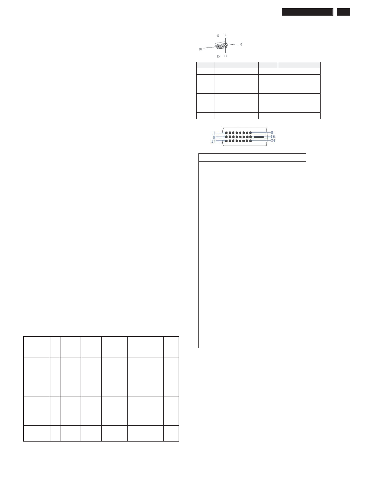
PIN No. SIGNAL PIN No. SIGNAL
1 Red 9 DDC +3.3V or +5V
2 Green/ SOG 10 Logic GND
3 Blue 11 Sense (GND)
4 Sense (GND) 12 Bi-directional data
5 Cable Detect (GND) 13 H/H+V sync
6 Red GND 14 V-sync
7 Green GND 15 Data clock
8 Blue GND
ʳʳ
Susceptibility of display to external environment
Operating
- Temperature : 0 to 40 degree C
- Humidity :80% max
- Altitude :
0-3658m
- Air pressure : 600-1100 mBAR
Storage
- Temperature : -20 to 60 degree C
- Humidity : 95% max
- Altitude : 0-12192m
- Air pressure : 300-1100 mBAR
Note: recommend at 5 to 35qC, Humidity less than 60 %
Pin No. Description
1 T.M.D.S. data22 T.M.D.S. data2+
3 T.M.D.S. data2 shield
4 No Connect
5 No Connect
6 DDC clock
7 DDC data
8 No Connect
9 T.M.D.S. data110 T.M.D.S. data1+
11 T.M.D.S. data1 shield
12 No Connect
13 No Connect
14 +5V Power
15 Ground (for +5V)
16 Hot plug detect
17 T.M.D.S. data018 T.M.D.S. data0+
19 T.M.D.S. data0 shield
20 No Connect
21 No Connect
22 T.M.D.S clock shield
23 T.M.D.S. clock+
24 T.M.D.S. clock-
4 241B4LPY LCD
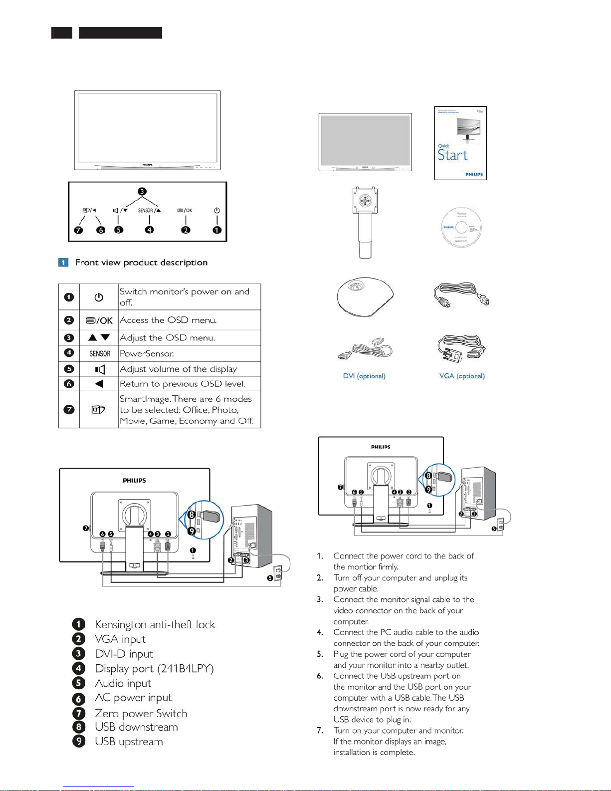
Installation
Front View Product Description Accessory Pack
Unpack all the parts
Connecting to Your PC
1) Connect the power cord to the back of the monitor firmly.
(Philips has pre-connected VGA cable for the first installation.
ʳ
Rear Vi
ew
ʳ

241B4LPY LCD 5
Troubleshooting
ʳ
6 241B4LPY LCD
Troubleshooting
241B4LPY LCD 7
On-Screen Display
Description of the On Screen Display
ʳ
What is the On-Screen Display?
ʳ
On-Screen Display (OSD) is a feature in all Philips LCD monitors. It allows an end user to adjust screen performance or
select functions of the monitors directly through an on-screen instruction window. A user friendly on screen display
interface is shown as below :
ʳ
ʳ
Basic and simple instruction on the control keys.
ʳ
In the OSD shown above users can press buttons at the front bezel of the monitor to move the cursor, to
confirm the choice or change.
ʳ
ʳʳ
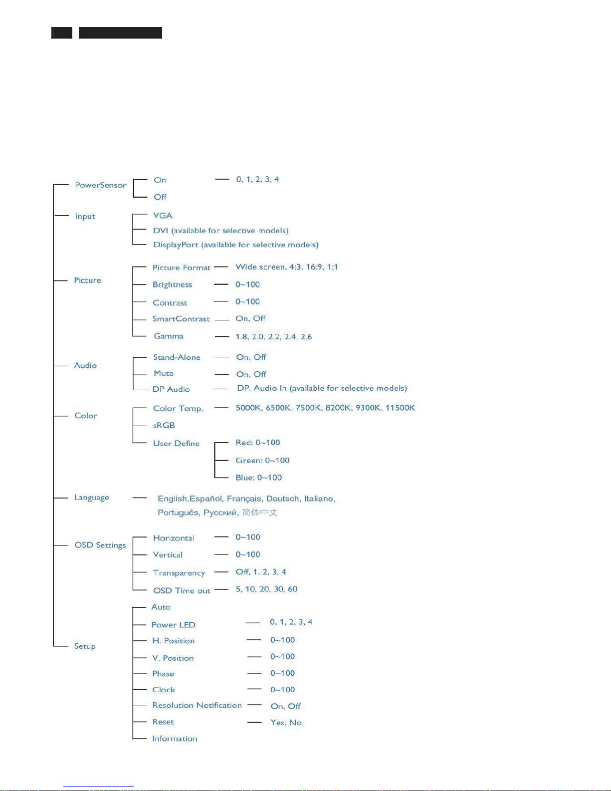
8 241B4LPY LCD
On-Screen Display
The OSD Tree
ʳ
Below is an overall view of the structure of the On-Screen Display. You can use this as a reference when you want to work
your way around the different adjustments later on.
ʳ
ʳ
241B4LPY LCD 9
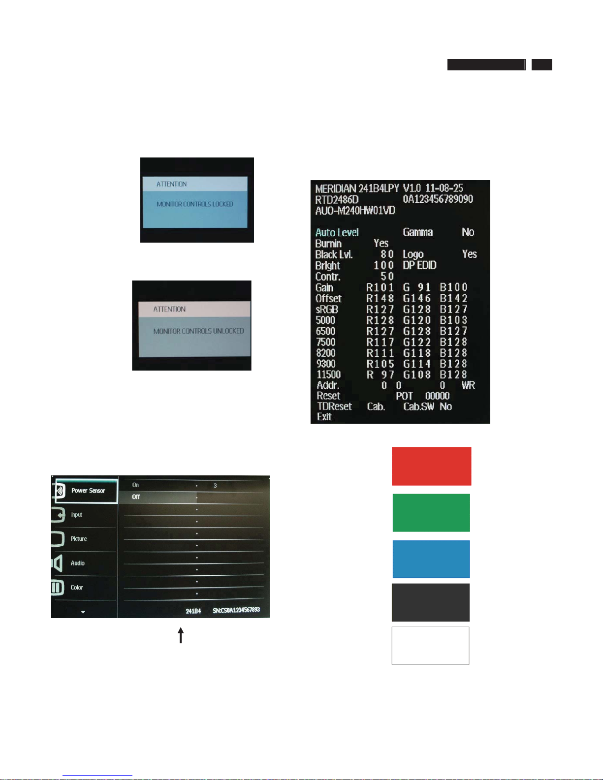
/RFN8QORFN$JLQJ)DFWRU\0RGH
To lock/unlock OSD FUNCTION(User Mode)
The OSD function can be locked by pressing"OK"button(1) for more than 10
seconds, the screen shows following windows for 4 seconds. Every time
when you press"OK" button, this message appears on the screen
automatically .
Unlock OSD function
Unlocked OSD function can be released by pressing "OK" button for more
than 10 seconds again.
$FFHVV)DFWRU\0RGH
1). Turn off monitor.
2).[Push "EXIT" & "MENU" buttons at the same time and hold them]+[Press
"power" button until comes out "Windows screen" ]=> then release all
buttons
3).Press "MENU" button, wait until the OSD menu with Characters
"MERIDIAN 241B4LPY V1.0 2011-08-25” (below OSD menu) come on the
Screen of the monitor.
Factory Mode indicator
Factory Menu
Cursor can move on gray color area
Hot key function: by pressing " UP " and " DOWN " key Simultaneously at
User Mode (or Factory Mode) (PS: The Of fset R G B function can be used
on reduce or eliminate snowy noise on the background when the resolution
of video signal is 1280*1024vertical 75Hz. Slightly increase or decrease the
value until snowy noise completely disappear .
$FFHVV$JLQJ0RGH
Step 1 : Access Factory Mode then enter Factory Menu.
Step 2 : By pressing " UP" and " DOWN " key to Burning Icon. Press
"MENU then press " UP" and "DOWN " key to turn on Aging Mode.
Step 3 : Disconnect interface cable between Monitor and PC.
After 3 seconds,
bring up:
repeatly
Connect Signal cable again=> go back to normal display
10 241B4LPY LCD
Philips Pixel Defect Policy
ʳ
Philips' Flat Panel Monitors Pixel Defect Policy
ʳ
Black Dot Defects Black dot defects appear as pixe
ls or sub pixels that are
always dark or 'off'. That is, a dark dot is a sub-pixel that stands out on the
screen when the monitor displays a light pattern. These are the types of
black dot defects:ʳ
Philips strives to deliver the highest quality products. We use some of the
industr
y's most advanced manufacturing processes and practice stringent
quality control. However, pixel or sub pixel defects on the TFT LCD panels
used in flat panel monitors are sometimes unavoidable. No manufacturer
can guarantee that all panels will be free from pixel defects, but Philips
guarantees that any monitor with an unacceptable number of defects will be
repaired or replaced under warranty. This notice explains the different types
of pixel defects and defines acceptable defect levels for each type. In order
to qualify for repair or replacement under warranty, the number of pixel
defects on a TFT LCD panel must exceed these acceptable levels. For
example, no more than 0.0004% of the sub pixels on a 19" XGA monitor may
be defective. Furthermore, Philips sets even higher quality standards for
certain types or combinations of pixel defects that are more noticeable than
others. This policy is valid worldwide.
Pixels and Sub pixels
A pixel, or picture element, is composed of three sub pixels in the primary
colors of red, green and blue. Many pixels together form an image. When all
sub pixels of a pixel are lit, the three colored sub pixels together appear as a
single white pixel. When all are dark, the three colored sub pixels together
appear as a single black pixel. Other combinations of lit and dark sub pixels
appear as single pixels of other colors.
ʳTy pes of Pixel Defects
ʳ
Pixel and sub pixel defects appear on the screen in different ways. There are
two categories of pixel defects and several types of sub pixel defects within
each category. ʳ
Bright Dot Defects Bright dot defects appear as pixels or sub pixels that are
always lit or 'on'. That is, a bright dot is a sub-pixel that stands out on the
screen when the monitor displays a dark pattern. There are the types of
bright dot defects:ʳ
ʳ
ʳ
One lit red, green or
blue sub pixelʳ
Two adjacent lit sub
pixels:
- Red + Blue =
Purple
- Red + Green =
Yellow
- Green + Blue =
Cyan (Light Blue)!
Three adjacent lit sub
pixels (one white
pixel)ʳ
ʳ
A red or blue bright dot must be more than 50 percent brighter
than neighboring dots while a green bright dot is 30 percent
brighter than neighboring dots.ʳ
ʳ
One dark sub pixelʳ Two or three adjacent dark sub pixelsʳ
Proximity of Pixel Defects
ʳ
Because pixel and sub pixels defects of the same type that are near to one
another may be more noticeable, Philips also specifies tolerances for the
proximity of pixel defects.
Pixel Defect Tolerances
ʳ
In order to qualify for repair or replacement due to pixel defects during the
warranty period, a TFT LCD panel in a Philips flat panel monitor must have
pixel or sub pixel defects exceeding the tolerances listed in the following
tables.ʳ
BRIGHT DOT DEFECTSʳ
ACCEPTABLE
LEVEL ʳ
MODELʳ
241B4LP(Y)ʳ
1 lit subpixelʳ 3ʳ
2 adjacent lit subpixelsʳ 1ʳ
3 adjacent lit subpixels (one white pixel)ʳ 0ʳ
Distance between two bright dot defects*ʳ >15mmʳ
Total bright dot defects of all typesʳ 3ʳ
BLACK DOT DEFECTSʳ
ACCEPTABLE
LEVEL ʳ
MODELʳ
241B4LP(Y)
ʳ
1 dark subpixelʳ 5 or fewerʳ
2 adjacent dark subpixelsʳ 2 or fewerʳ
3 adjacent dark subpixelsʳ 0 ʳ
Distance between two black dot defects*ʳ >15mmʳ
Total black dot defects of all typesʳ 5 or fewerʳ
TOTAL DOT DEFECTSʳ
ACCEPTABLE
LEVEL ʳ
MODELʳ
241B4LP(Y)
ʳ
Total bright or black dot defects of all
typesʳ
5 or fewerʳ
Note:
* 1 or 2 adjacent sub pixel defects = 1 dot defect
241B4LPY LCD 11
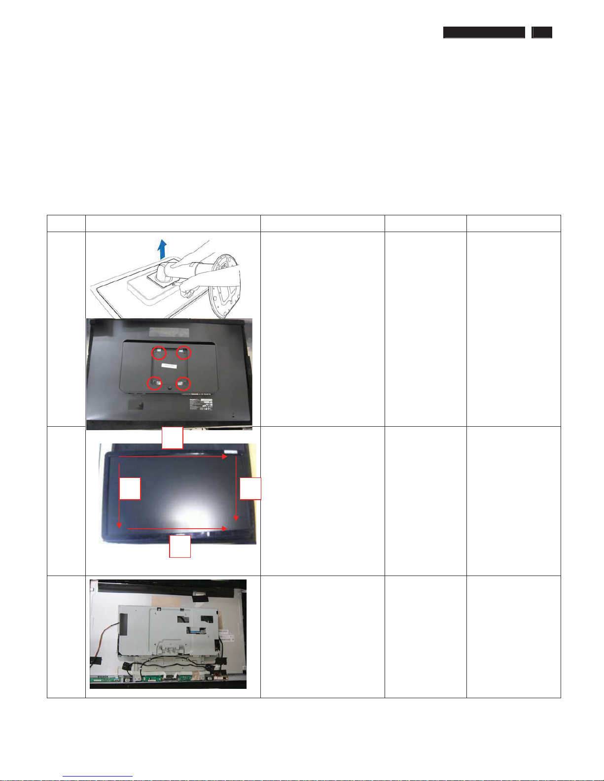
Mechanical Instruction
Preparation before disassemble
1.Clean the room for disassemble
2.Identify the area for monitor
3.Check the position that the monitors be placed and the quantity of the monitor ;prepare the area for material flow;
according to the actual condition plan the disassemble layout
4.Prepare the implement, equipments, materials as bellow:
1) Press-fixture
2) working table
3) Screw-driver
4) knife*1
5) glove
6) cleaning cloth
7) ESD protection
item picture Operation Tool Notes
1
Disassemble the Stand.
While keeping the release
button pressed, tilt the base
and slide it out.
Disassembly 4 screws,
Take off the stand .
Screw-driver
2 Turn over the monitor ,
Bring the Bezel from the
monitor
When disassembly
the bezel ,
notice don’t bend
the C/B .
man must wear
glove
The purpose is
loose the BZL
3 Remove the RC cover
4
3
2
1
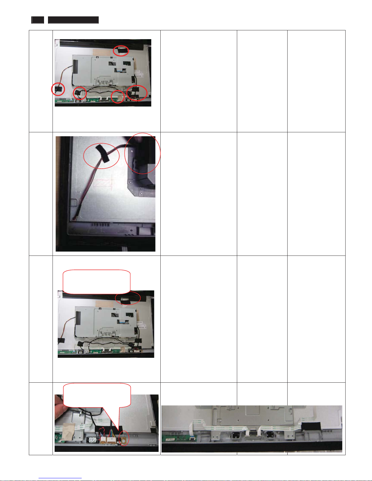
12 241B4LPY LCD
4 Remove all the Tapes on
each cable
5 Disassembly the Mylar on
lamp cables and draw the
lamp cables
6 Unlock the FFC by using
two hands(see note).
Please carefully use
two hands(one hand
presses the lockinglatch of FFC cable’s
housing, and at the
same time another
hand pulls out the
FFC cable.) for this
step to avoid from
deforming the
terminals of
positive-locking type
FFC cable.
7 Remove speaker and
remove the Audio BD
Screw-driver
The locking-latch
of FFC cable’s
Disassembly the
Au
d
io bd screw*1
241B4LPY LCD 13
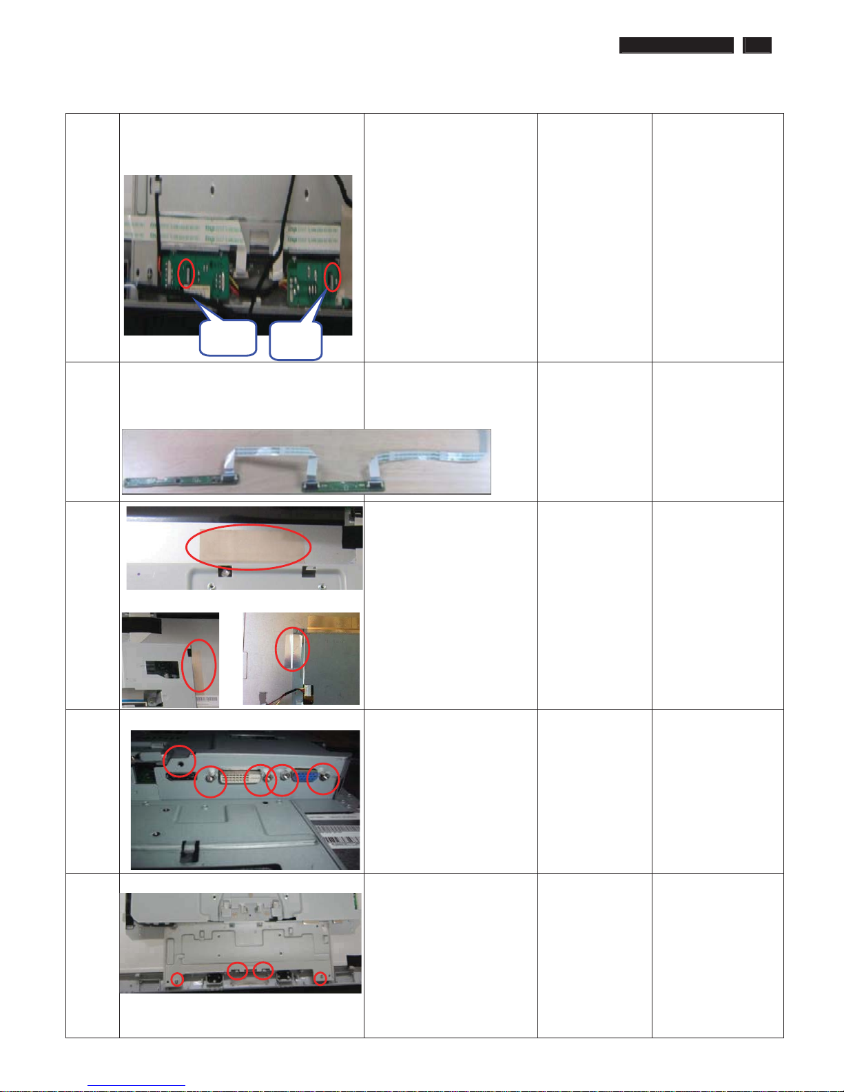
8 Remove IR bd TX bd
9 Disassemble the Control bd
and LED bd out from the
Bezel
10 Remove all the AL tapes
7;EG
,5
11 Disassemble the D-SUB
DVI and DP screws
Screw-driver
12 Take the Main-BKT out from
the Bezel
14 241B4LPY LCD
13 Turn over the Main-BKT
and Disassemble all the
PCBA bd screws*8
14 Remove the USB bd and
USB cable
15 Remove the AC-Switch and
all cables on Power bd
Screw-knife
16 Remove the AC-Switch
cover on Main-BKT
17 Take the PCBA out from
Main-BKT and then put it
on the cushion
241B4LPY LCD 15
Color Adjustment
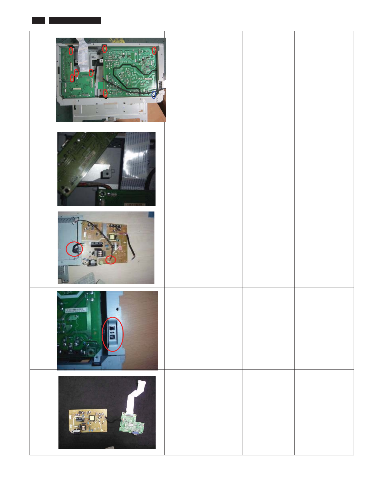
Alignment procedure
)LJ
1. Turn on the LCD monitor
2. Turn on the Timing/pattern generator. See Fig.1
3. Preset LCD co
lor Analyzer CA-1 10
-Remove the lens protective cover of probe CA-A30.
-Set measuring/viewing selector to measuring position for reset
analyzer .(zero calibration) as Fig.2
- Turn on the color analyzer (CA-1 10)
-Press 0-CAL button to starting reset analyzer .
Fig.5
5.Display
Press "UP" or "DOWN" button to select . Change the value
by "UP" or "DOWN" key until the X, Y co-ordinates as below
5.1 Color temperature adjustment
Fig. 1 Fig.2
There are six factory preset white color 11500K, 9300K, 8200K, 7500K,
6500K, sRGB, 5000K
4. Access F
actory Mode
Align by
Philips PerfecTune (also called FGA) function.
1). Turn off monitor.
Appl
y full white pattern, with brightness in 100 % position and the contrast
control at 50 % position.
2). [Push "AU
TO" & "MENU" buttons at the same time and hold them]
+[Press "power" button untill comes out "Windows screen" ]
The 1931 CIE Chromaticity (color triangle) diagram (x , y) coordinate for
the screen center should be:
=> then release
all buttons
3).Press "MENU button, wait until the OSD menu with
Characters " MERIDIAN 241B4LPY V1.0 2011-08-25” (below OSD menu)
come on the Screen of the monitor as shown in Fig3.
Product specification
CIE coordinates (x,y)
11500K x = 0.270 ± 0.02
y = 0.281 ± 0.02
PerfecTune II
9300K x = 0.283 ± 0.02
y = 0.297 ± 0.02
PerfecTune II
8200K x = 0.291 ± 0.02
y = 0.306 ± 0.02
PerfecTune II
7500K x = 0.298 ± 0.02
y = 0.314 ± 0.02
PerfecTune II
6500K/sRGB x = 0.313 ± 0.02
y = 0.329 ± 0.02
PerfecTune II
sRGB x = 0.313 ± 0.02
y = 0.329 ± 0.02
PerfecTune II
5000K x = 0.345 ± 0.02
y = 0.357 ± 0.02
PerfecTune II
Factory Mode indicator
Production alignment spec
)LJ
CIE coordinates (x,y)
11500K x = 0.270 ± 0.006
y = 0.281 ± 0.006
PerfecTune II
9300K x = 0.283 ± 0.006
y = 0.297 ± 0.006
PerfecTune II
8200K x = 0.291 ± 0.006
y = 0.306 ± 0.006
PerfecTune II
7500K x = 0.298 ± 0.006
y = 0.314 ± 0.006
PerfecTune II
6500K/sRGB x = 0.313 ± 0.006
y = 0.329 ± 0.006
PerfecTune II
sRGB x = 0.313 ± 0.006
y = 0.329 ± 0.006
PerfecTune II
5000K x = 0.345 ± 0.006
y = 0.357 ± 0.006
PerfecTune II
4). Press button, then select factory mode indicator by "MENU" "LEFT"
or "RI
GHT" button .Press"MENU" button to bring up submenu
windows as below:
Quality Inspection specification
CIE coordinates (x,y)
9300K x = 0.283 ± 0.015
y = 0.297 ± 0.015
6500K/sRGB x = 0.313 ± 0.015
y = 0.329 ± 0.015
16 241B4LPY LCD
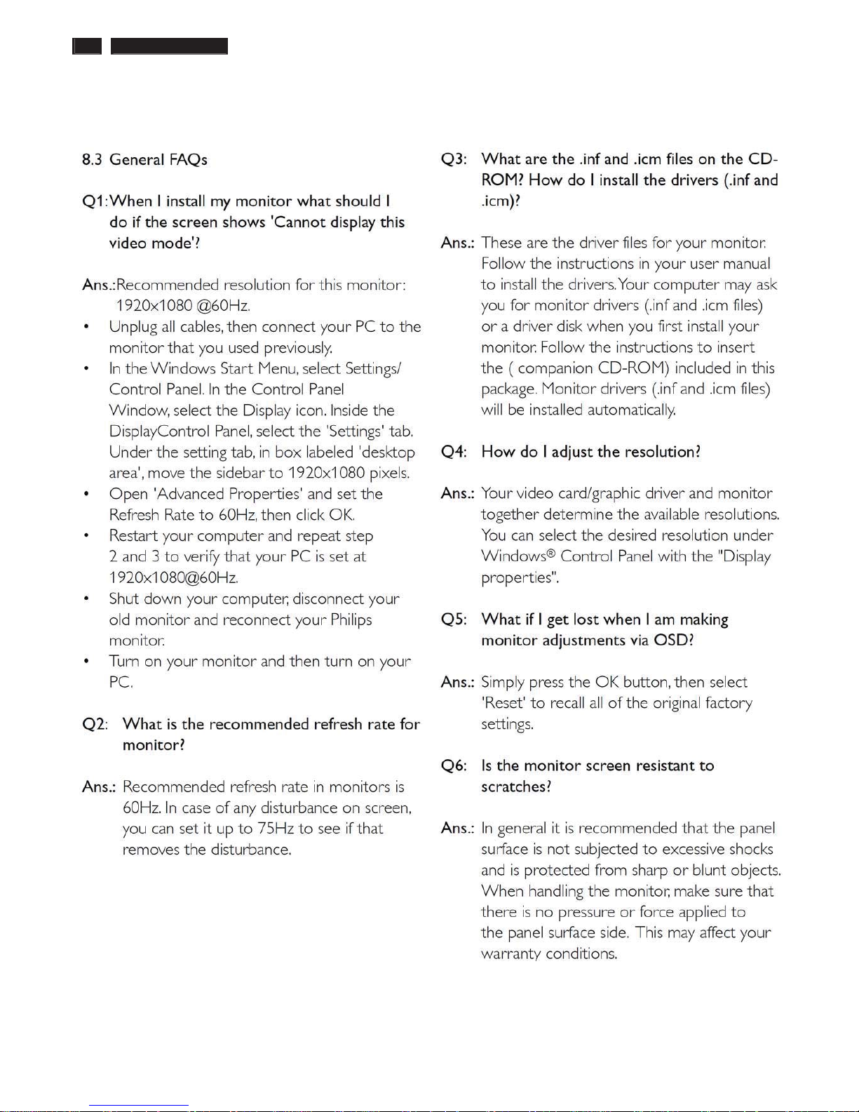
FAQs (Frequently Asked Questions)
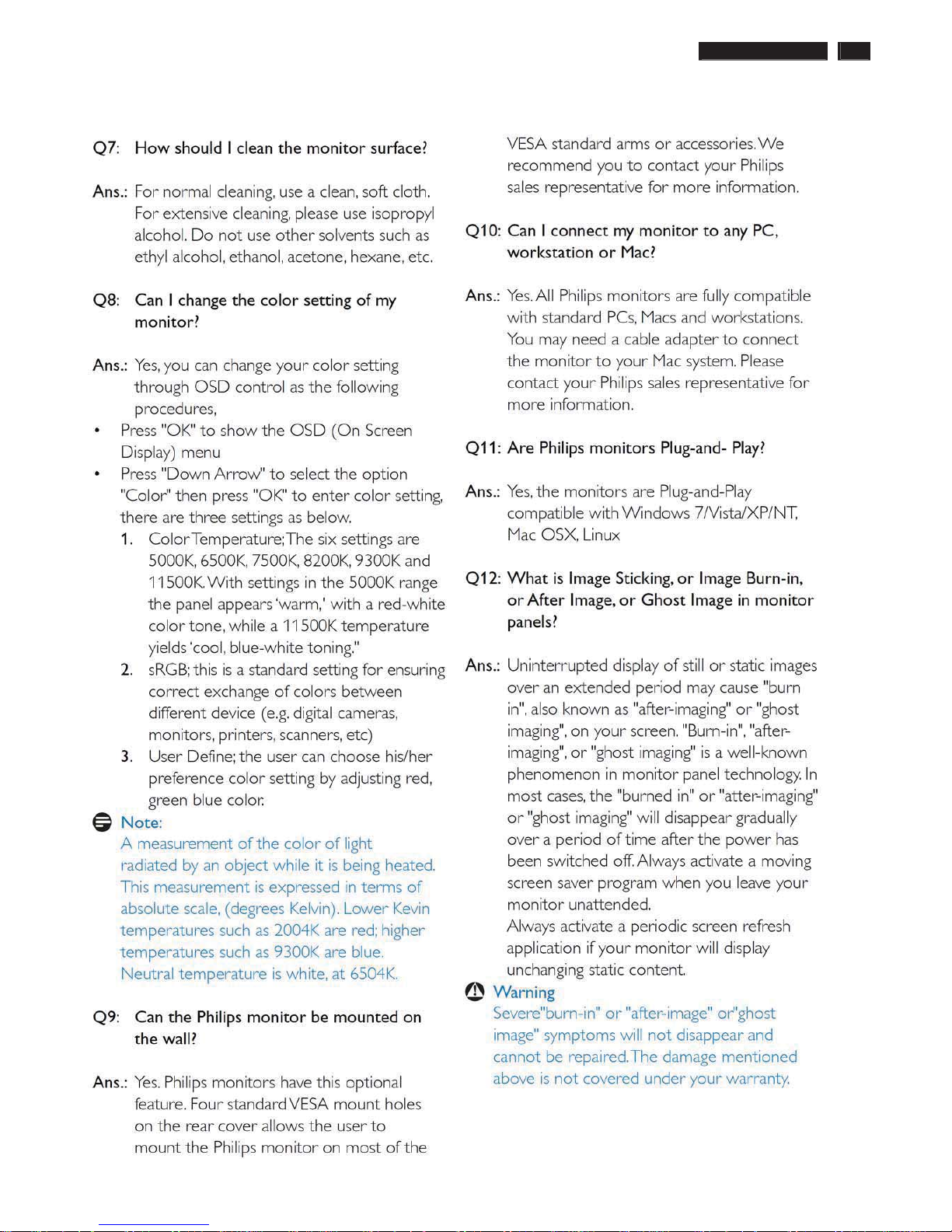
241B4LPY LCD 17
FAQs (Frequently Asked Questions)
18 241B4LPY LCD
Electrical Instructions
Electrical characteristics
1. Interface signals
1.1 D-Sub Analog
Input signal: Video, Hsync., Vsync
Video: 0.7 Vp-p, input impedance, 75 ohm @DC
Sync.: Separate sync TTL level , input impedance 2.2k ohm terminate
Hsync Positive/Negative
Vsync Positive/Negative
Composite sync TTL level, input impedance 2.2k ohm terminate
Sync on green video 0.3 Vp-p Negative (Video 0.7 Vp-p Positive)
1.2 DVI-D Digital(optional for 241S4L / 241S4LA / 241S4LC / 241B4LP )
Input signal: Single TMDS link (Three channels: RX0-/+, RX1-/+, RX2-/+)
1.3 Display port (241S4LY / 241B4LPY)
2. Interface
2.1 D-Sub Cable
Length : 1.8 M +/- 50 mm
Fix with monitor when packing, with transplant pin protective cover.
Connector type : D-Sub male with DDC2B pin assignments.
Blue connector thumb-operated jack screws
2.2 DVI Cable
The input signals are applied to the display through DVI-D cable.
Length : 1.8 M +/- 50 mm
Connector type : DVI-D male with DDC-2B pin assignments
White connector thumb-operated jackscrews
With transplant pin protective cover.
2.3 Display port cable
Length : Please refer to cable bundle summary file
Connector type : DP1.4
type A cable-connector
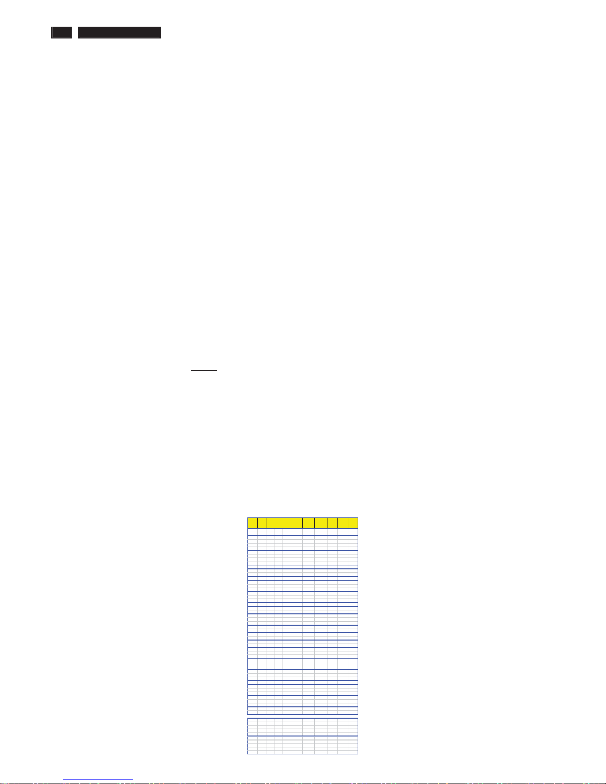
3. Timing requirement
3.1 Factory Preset mode definitions:
3.1.1 Perfect FOS while presenting those timings.
3.1.2 Will specify those timing in User's Manual
3.2 Preset mode definition:
3.2.1 Need to support those timings.
3.2.2 Perfect FOS after auto adjustment.
3.3 User mode
3.3.1 Can save those timing that not in Preset mode and can be showed
(not over scalar or Panel spec.)
3.3.2 It needs to reserve the 10 timings space in memory size.
3.3.3 Factory modes and preset modes are defined in the enclosed timing table file
Support
Timing
Auto
Pixel Rate
( MHz )
Horizontal
( KHz )
Vertical
( Hz )
V_Total
( Line )
Polarity
( H / V )
1
DOS 640x350/70 25.175 31.469 70.086 449
p / n
2
DOS 720x400/70 28.322 31.469 70.087 449
n / p
3
DMT
4:3
640x480/60 25.175 31.469 59.940 525
n / n
4
MAC 640x480/67 30.240 28.571 66.667 525
n / n
5
DMT
4:3
640x480/72 31.500 37.861 72.809 520
n / n
6
DMT
4:3
640x480/75 31.500 37.500 75.000 500
n / n
7
DMT
4:3
800x600/56 36.000 35.156 56.250 625
p / p
8
DMT
4:3
800x600/60 40.000 37.879 60.317 628
p / p
9
DMT
4:3
800x600/72 50.000 48.077 72.188 666
p / p
10
DMT
4:3
800x600/75 49.500 46.875 75.000 625
p / p
11
MAC 832x624/75 57.280 49.722 74.546 667
P / p
12
CVT 960x720/60 55.750 44.671 59.721 748
n / p
13
CVT 960x720/75 71.250 56.369 74.660 755
n / p
14
1024x600/60 48.964 37.320 60.000 622
n / p
15
DMT
4:3
1024x768/60 65.000 48.363 60.004 806
n / n
16
DMT
4:3
1024x768/70 75.000 56.476 70.069 806
n / n
17
DMT
4:3
1024x768/75 78.750 60.023 75.029 800
p / p
18
CVT 1152x864/60 81.750 53.783 59.959 897
n / p
19
1152x864/70 94.499 63.851 70.012 912
p / p
20
DMT 1152x864/75 108.000 67.500 75.000 900
p / p
21
MAC 1152x870/75 100.001 68.682 74.980 916
n / n
22
SUN 1152x900/66 94.500 61.846 66.004 937
p / p
23 SUN 1152x900/76 108.000 71.809 76.149 943 p / p
24
CV
T
16:9
1280x720/60 74.250 45.000 60.000 750
p / p
25
CVT
16:9
1280x720/70 89.040 52.500 70.000 750
n / p
26
CVT
16:9
1280x720/75 95.750 56.456 74.777 755
n / p
27
DMT 1280x768/60 79.500 47.776 59.870 798
n / p
28
DMT 1280x768/75 102.250 60.289 74.893 805
n / p
29
CVT 1280x800/60 83.500 49.702 59.810 831
n / p
30
CVT 1280x800/75 106.500 62.795 74.934 838
n / p
31
DMT
4:3
1280x960/60 108.000 60.000 60.000 1000
p / p
32
CVT
4:3
1280x960/75 130.000 75.231 74.857 1005
n / p
33
DMT
5:4
1280x1024/60 108.000 63.981 60.020 1066
p / p
34
DOS
5:4
1280x1024/72 130.223 76.020 71.447 1064
p / p
35
DMT
5:4
1280x1024/75 135.000 79.976 75.025 1066
p / p
36
DMT
16:9
1360x768/60 85.500 47.712 60.015 795
p / p
37
CVT
16:9
1360x768/75 109.000 60.288 74.891 805
n / p
38
DMT
16:9
1366x768/60 85.500 47.712 59.790 798
p / p
39
DMT 1440x900/60_RB 88.750 55.469 59.901 926
p / n
40
DMT 1440x900/60 106.500 55.935 59.887 934
n / p
41
DMT 1440x900/75 136.750 70.635 74.984 942
n / p
42
DMT
4:3
1600x1200/60 162.000 75.000 60.000 1250
p / p
43
DMT
16:10
1680x1050/60_RB 119.000 64.674 59.883 1080
p / n
44
DMT
16:10
1680x1050/60 146.250 65.290 59.954 1089
n / p
45
DMT
16:10
1680x1050/75 187.000 82.306 74.892 1099
n / p
46
CVT
16:9
1920x1080/60_RB 138.500 66.587 59.934 1111
p / n
47
DM
T
16:9
1920x1080/60 148.500 67.500 60.000 1125
p / p
48
CVT
16:9
1920x1080/60 173.000 67.158 59.963 1120
n / p
49
DMT
16:10
1920x1200/60_RB 154.000 74.038 59.950 1235
p / n
50
DMT
16:10
1920x1200/60 193.250 74.556 59.885 1245
n / p
51
576P 720x576/50
27.000 31.250
50.000
625
52
576i 720x576/50
13.500 15.625
50.000
625
53
720P 1280x720/50 74.250 37.500 50.000 750
54
1080i 1920x1080/50 74.250 28.125 50.000 1125
55
1080P 1920x1080/50 148.500 56.250 50.000 1125
56
480P 720x480/60 27.000 31.468 60.000 525
57
480i 720x480/60 13.500 15.734 60.000 525
58
720P 1280x720/60 74.250 45.000 60.000 750
59
1080i 1920x1080/60 74.250 33.750 60.000 1125
241SB4 support
Resolution
Extra Supported Video Timing ( Video Timing Don’t Care Picture Quality )
60
1080P 1920x1080/60 148.500
67.500 60.000 1125
241B4LPY LCD 19
Electrical Instructions
White color adjustment
There are three factory preset white color 9300K, 6500K, sRGB.
Apply full gray64 pattern, with brightness in 100 % position and the contrast control at 50 % position.The 1931 CIE
Chromaticity (color triangle) diagram (x ,y) coordinate for the screencenter should be:
Product specification
CIE coordinates (x,y)
11500K x = 0.270 ± 0.02
y = 0.281 ± 0.02
PerfecTune II
9300K x = 0.283 ± 0.02
y = 0.297 ± 0.02
PerfecTune II
8200K x = 0.291 ± 0.02
y = 0.306 ± 0.02
PerfecTune II
7500K x = 0.298 ± 0.02
y = 0.314 ± 0.02
PerfecTune II
6500K/sRGB x = 0.313 ± 0.02
y = 0.329 ± 0.02
PerfecTune II
sRGB x = 0.313 ± 0.02
y = 0.329 ± 0.02
PerfecTune II
5000K x = 0.345 ± 0.02
y = 0.357 ± 0.02
PerfecTune II
Production alignment spec.
CIE coordinates (x,y)
11500K x = 0.270 ± 0.006
y = 0.281 ± 0.006
PerfecTune II
9300K x = 0.283 ± 0.006
y = 0.297 ± 0.006
PerfecTune II
8200K x = 0.291 ± 0.006
y = 0.306 ± 0.006
PerfecTune II
7500K x = 0.298 ± 0.006
y = 0.314 ± 0.006
PerfecTune II
6500K/sRGB x = 0.313 ± 0.006
y = 0.329 ± 0.006
PerfecTune II
sRGB x = 0.313 ± 0.006
y = 0.329 ± 0.006
PerfecTune II
5000K x = 0.345 ± 0.006
y = 0.357 ± 0.006
PerfecTune II
Quality Inspection specification:
CIE coordinates (x,y)
9300K x = 0.283 ± 0.015
y = 0.297 ± 0.015
6500K/sRGB x = 0.313 ± 0.015
y = 0.329 ± 0.015
sRGB x = 0.313 ± 0.015
y = 0.329 ± 0.015
20 241B4LPY LCD
Service tool-Hardware
PCM code 12NC
5E.L8215.001 996510019769
241B4LPY LCD 21
Service tool-Software
FW writing tool: RTD tool V6.7
DDC writing tool: Q-EDID-V30
22 241B4LPY LCD
DDC Instructions
DDC Data Re-programming
In case the DDC data memory IC or main EEPROM which storage all factory settings were
replaced due to a defect, the serial numbers have to be re-programmed "Analog
DDC IC, Digital DDC IC & EEPROM".
It is advised to re-soldered DDC IC and main EEPROM from the old board onto the new
board if circuit board have been replaced, in this case the DDC data does not need to be
re-programmed.
Additional information
Additional information about DDC (Display Data Channel) may be obtained from Video
Electronics Standards Association (VESA).
Extended Display Identification Data(EDID) information may be also obtained from
VESA.
Configuration and procedure
"PI-EDID" The software is provided by IMS to upgrade the firmware of CPU.
PI-EDID Tools is for the interface between "Parallel Port of PC" and "15 pin-D-SUB
connector of Monitor".
It is a windows-based program, which cannot be run in MS-DOS.
System and equipment requirements
1. An Pentium (or above) personal computer or compatible.
2. Microsoft operation system Windows 95/98/2000/XP and Port95NT.exe.
3. EDID Software "QEDID.exe"
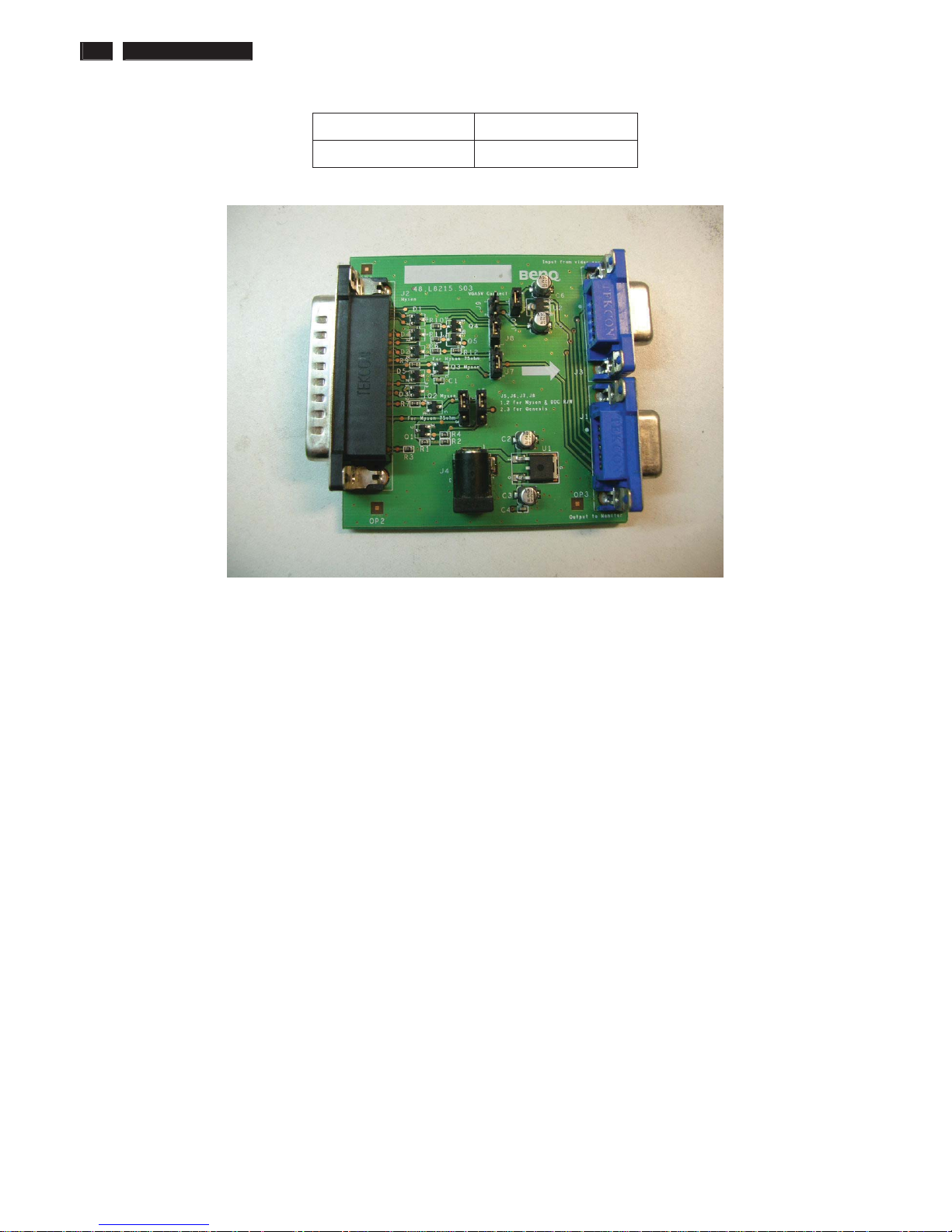
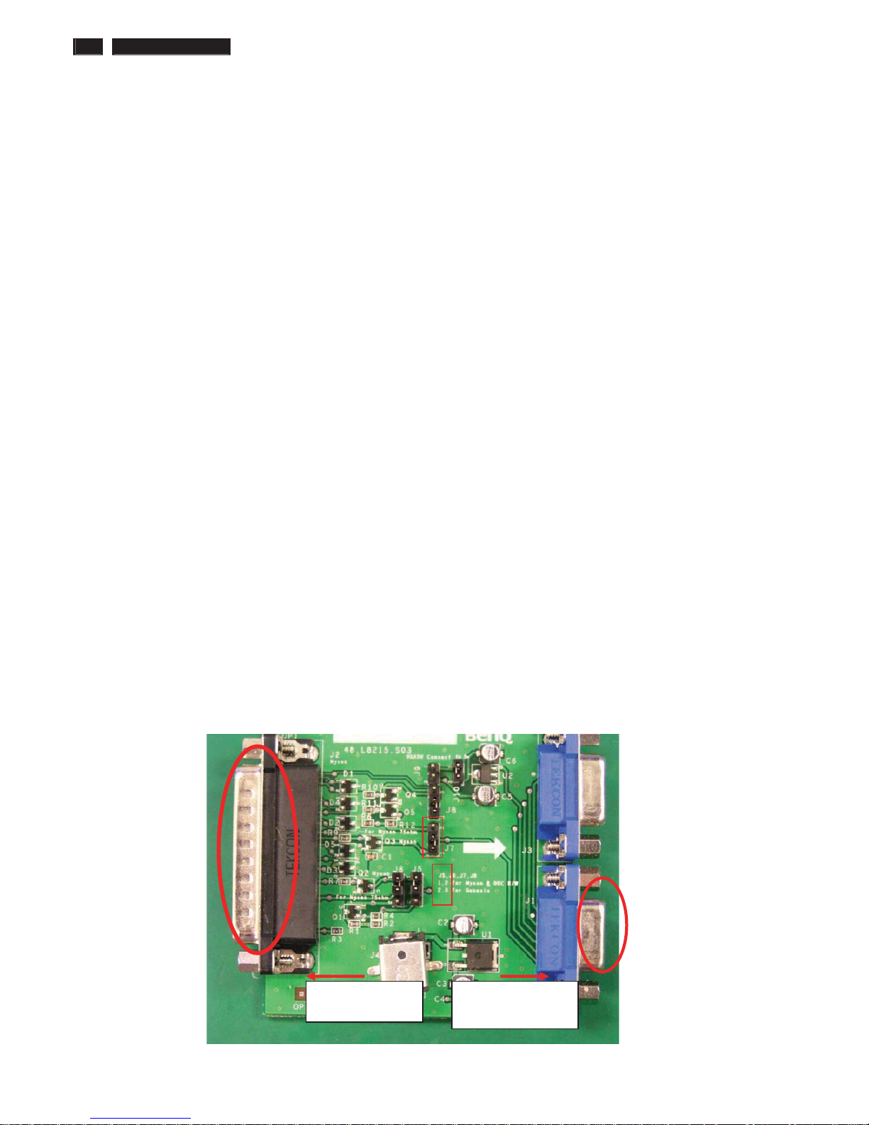
4. ISP boardas shown in Fig. 1
And I2C Board Jump wire should follow J10 (short), J9 (open), J5/J6/ (1and 2 pin short)
J7/J8 (1 and 2 pin short)
3
2
1
2
Connected to Display
Signal Cable
Connected to print
cord and PC
Fig.1
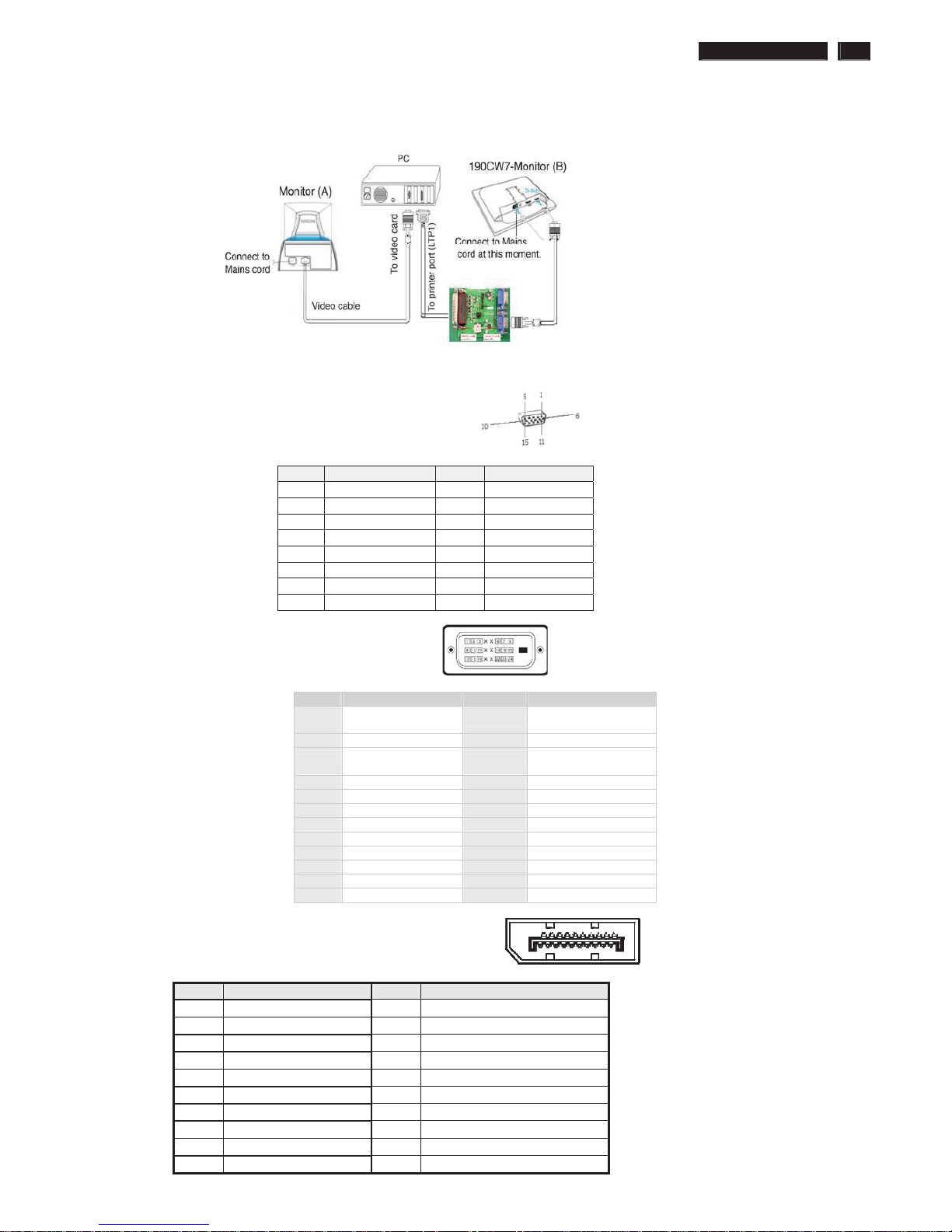
241B4LPY LCD 23
DDC Instructions
5. Connect and Mains cord to Monitor as shown in Fig.2.
Fig.2
Pin assignments:
A. 15-pin D-Sub Connector
B. Input DVI Connector pin
Pin Signal Assignment Pin Signal assignment
1
TMDS RX2-
13 Floating
2 TMDS RX2+ 14 +5V Power
3 TMDS Ground 15
Self-test (Cable
detector)
4 Floating 16 Hot Plug Detect
5 Floating 17 TMDS RX06 DDC Clock 18 TMDS RX0+
7 DDC Data 19 TMDS Ground
8 Floating 20 Floating
9 TMDS RX1- 21 Floating
10 TMDS RX1+ 22 TMDS Ground
11 TMDS Ground 23 TMDS Clock+
12 Floating 24 TMDS Clock-
C. Input Display Port Connector pin
Pin Signal Assignment Pin Signal Assignment
1 Lane0 P 11
Ground
2Ground 12
Lane3 N
3 Lane0 N 13 Ground
4 Lane1 P 14 EDID WP
5Ground 15AUX_CH P
6 Lane1 N 16 Ground
7 Lane2 P 17AUX_CH N
8Ground 18
Hot Plu
g
Detect
9 Lane2 N 19
Return
10
Lane3 P
20
DP
_
PWR
PIN No. SIGNAL PIN No. SIGNAL
1 Red 9 DDC +3.3V or +5V
2 Green/ SOG 10 Logic GND
3 Blue 11 Sense (GND)
4 Sense (GND) 12 Bi-directional data
5 Cable Detect (GND) 13 H/H+V sync
6 Red GND 14 V-sync
7 Green GND 15 Data clock
8 Blue GND
ʳʳ
24 241B4LPY LCD
DDC Instructions
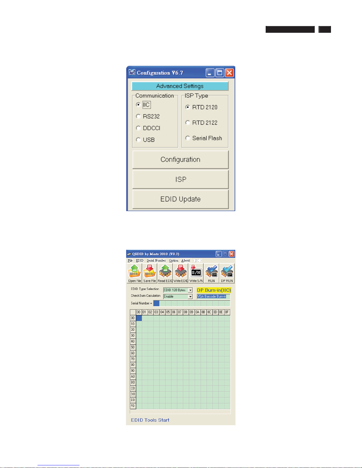
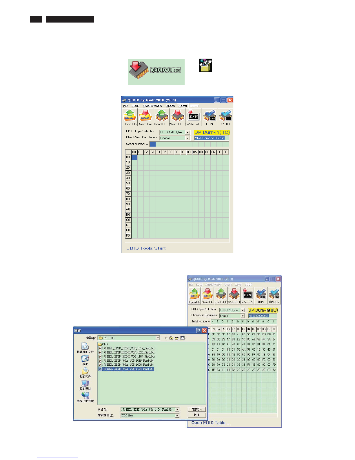
6. Setup the Philips-IMS EDID Tools program
Step 1: Open Q-EDID V030 Software into your folder as shown in Fig.3. and Fig.4.
ˤ˘˗˜˗ˆ˃˃ˁ˸˸
Fig.3
Fig.4
Step 2: Press “Open File” then chooses 241B4LPY DDC FILE
Fig.5
241B4LPY LCD 25
DDC Instructions
Step 3 : Load DDC file success as shown in Fig. 6 .
Fig.Step 4 : update Serial number and press enter to correct S/N number
shown as Fig.7 .
Fig.7
26 241B4LPY LCD
DDC Instructions
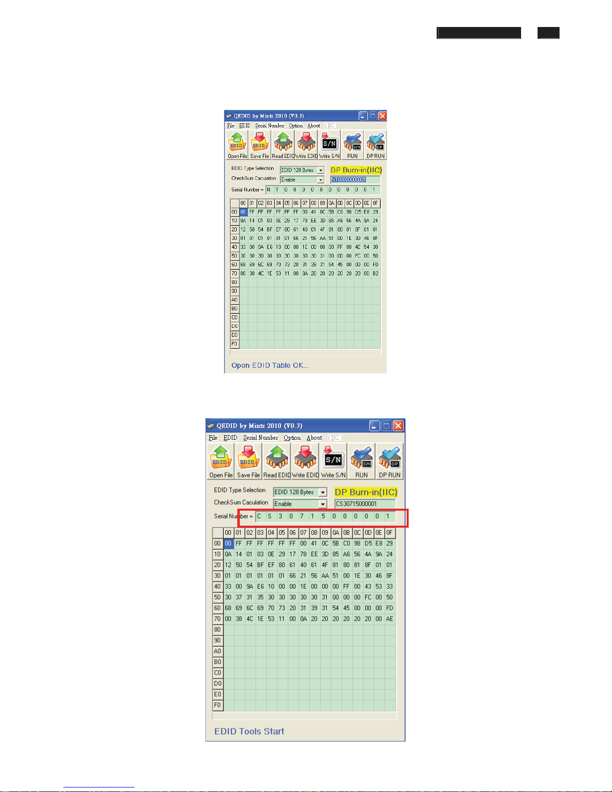
Step 5 : Press “RUN” to write EDID and serial number shown as Fig.8 .
Fig.8
Step 6 : EDID and serial number update success shown as Fig.9
Fig.9
241B4LPY LCD 27
DDC Instructions
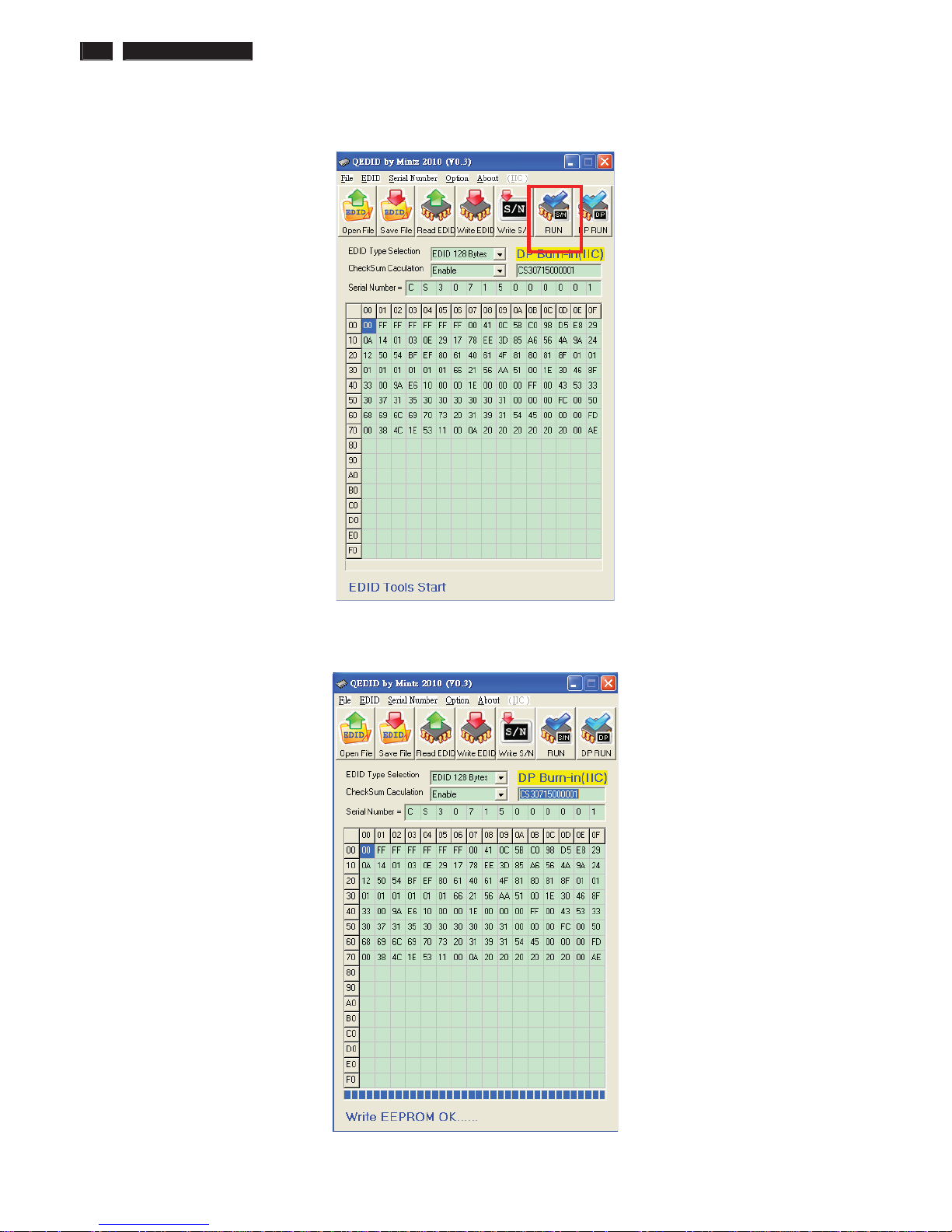
8. Press “Read EDID” to read EDID and serial number shown as Fig.10 . and check
Serial number is the same as we set.
Note: If not the same, please rewrite EDID S/N again.
Fig.10
9. Repeat Step2~7 for DVI port.
10. For DP, please use Factory function “DP EDID”. Select and enter to run this
function, if success it will show OK. shown as Fig.11

28 241B4LPY LCD
Fig.11
Serial Number Definition

241B4LPY LCD 29
DDC DATA
Analog DDC
StandarTiming Identification 1
Horizontal Active Pixels : 1152
Aspect Ratio : 4:3
Refresh Rate(Hz) : 60
StandarTiming Identification 2
Horizontal Active Pixels : 1280
Aspect Ratio : 16:9
Refresh Rate(Hz) : 60
StandarTiming Identification 3
Horizontal Active Pixels : 1280
Aspect Ratio : 5:4
Refresh Rate(Hz) : 60
StandarTiming Identification 4
Horizontal Active Pixels : 1440
Aspect Ratio : 16:10
Refresh Rate(Hz) : 60
StandarTiming Identification 5
Horizontal Active Pixels : 1680
Aspect Ratio : 16:10
Refresh Rate(Hz) : 60
StandarTiming Identification 6
Horizontal Active Pixels
Aspect Ratio :
Refresh Rate(Hz) :
StandarTiming Identification 7
Horizontal Active Pixels :
Aspect Ratio :
Refresh Rate(Hz) :
StandarTiming Identification 8
Horizontal Active Pixels :
Aspect Ratio :
Refresh Rate(Hz) :
Detailed Timing Description 1
Pixel Clock (kHz) : 148500
H Active (pixels) : 1920
H Blanking (pixels) : 280
V Active (lines) : 1080
V Blanking (lines) : 45
H Sync Offset (F Porch) (pixels) : 88
H Sync Pulse Width (pixels) : 44
V Sync Offset (F Porch) (lines) : 4
V Sync Pulse Width (lines) : 5
H Image Size (mm) : 531
V Image Size (mm) : 299
H Border (pixels) : 0
V Border (lines) : 0
Flag #1 : Bit 7 [0]
No-Interlaced
#2 : Bit 6,5 [0,0]
Normal display, no stereo
#3 : Bit 3,4 [1,1]
Digital Separate
#4 : Bit 2,1 [1,1]
Vsync Positive Polarity, Hsync Positive Polarity
Monitor Serial Number : CS0A123456789
Monitor Name : 241BLPY
Monitor Decription
Min. V Rate(Hz) : 56
Max. V Rate(Hz) : 76
Min. H Rate(kHz) : 30
Max. H Rate(kHz) : 83
Max. Pixel Clock(Mhz) : 210
**********************************************************************
EDID Data (128 bytes)
**********************************************************************
0: 00 1: FF 2: FF 3: FF 4: FF 5: FF 6: FF 7: 00
8: 41 9: 0C 10: B3 11: 08 12: 01 13: 00 14: 00 15: 00
16: 14 17: 15 18: 01 19: 03 20: 0E 21: 35 22: 1E 23: 78
24: CE 25: 2A 26: C5 27: A4 28: 56 29: 4F 30: 9E 31: 28
32: 12 33: 50 34: 54 35: BF 36: EF 37: 80 38: 71 39: 40
40: 81 41: C0 42: 81 43: 80 44: 95 45: 00 46: B3 47: 00
48: 01 49: 01 50: 01 51: 01 52: 01 53: 01 54: 02 55: 3A
56: 80 57: 18 58: 71 59: 38 60: 2D 61: 40 62: 58 63: 2C
64: 45 65: 00 66: 13 67: 2B 68: 21 69: 00 70: 00 71: 1E
72: 00 73: 00 74: 00 75: FF 76: 00 77: 43 78: 53 79: 30
80: 41 81: 31 82: 32 83: 33 84: 34 85: 35 86: 36 87: 37
88: 38 89: 39 90: 00 91: 00 92: 00 93: FC 94: 00 95: 32
96: 34 97: 31 98: 42 99: 4C 100: 50 101: 59 102: 0A 103: 20
104: 20 105: 20 106: 20 107: 20 108: 00 109: 00 110: 00 111: FD
112: 00 113: 38 114: 4C 115: 1E 116: 53 117: 15 118: 00 119: 0A
120: 20 121: 20 122: 20 123: 20 124: 20 125: 20 126: 00 127: AE
DVI DDC
StandarTiming Identification 1
Horizontal Active Pixels : 1152
Aspect Ratio : 4:3
Refresh Rate(Hz) : 60
StandarTiming Identification 2
Horizontal Active Pixels : 1280
Aspect Ratio : 16:9
Refresh Rate(Hz) : 60
StandarTiming Identification 3
Horizontal Active Pixels : 1280
Aspect Ratio : 5:4
Refresh Rate(Hz) : 60
StandarTiming Identification 4
Horizontal Active Pixels : 1440
Aspect Ratio : 16:10
Refresh Rate(Hz) : 60
StandarTiming Identification 5
Horizontal Active Pixels : 1680
Aspect Ratio : 16:10
Refresh Rate(Hz) : 60
StandarTiming Identification 6
Horizontal Active Pixels
Aspect Ratio :
Refresh Rate(Hz) :
StandarTiming Identification 7
Horizontal Active Pixels :
Aspect Ratio :
Refresh Rate(Hz) :
StandarTiming Identification 8
Horizontal Active Pixels :
Aspect Ratio :
Refresh Rate(Hz) :
Detailed Timing Description 1
Pixel Clock (kHz) : 148500
H Active (pixels) : 1920
H Blanking (pixels) : 280
V Active (lines) : 1080
V Blanking (lines) : 45
H Sync Offset (F Porch) (pixels) : 88
H Sync Pulse Width (pixels) : 44
V Sync Offset (F Porch) (lines) : 4
V Sync Pulse Width (lines) : 5
H Image Size (mm) : 531
V Image Size (mm) : 299
H Border (pixels) : 0
V Border (lines) : 0
Flag #1 : Bit 7 [0]
No-Interlaced
#2 : Bit 6,5 [0,0]
Normal display, no stereo
#3 : Bit 3,4 [1,1]
Digital Separate
#4 : Bit 2,1 [1,1]
Vsync Positive Polarity, Hsync Positive Polarity
Monitor Serial Number : CS0A123456789
Monitor Name : 241BLPY
Monitor Decription
Min. V Rate(Hz) : 56
Max. V Rate(Hz) : 76
Min. H Rate(kHz) : 30
Max. H Rate(kHz) : 83
Max. Pixel Clock(Mhz) : 170
**********************************************************************
EDID Data (128 bytes)
**********************************************************************
0: 00 1: FF 2: FF 3: FF 4: FF 5: FF 6: FF 7: 00
8: 41 9: 0C 10: B3 11: 08 12: 01 13: 00 14: 00 15: 00
16: 14 17: 15 18: 01 19: 03 20: 80 21: 35 22: 1E 23: 78
24: CE 25: 2A 26: C5 27: A4 28: 56 29: 4F 30: 9E 31: 28
32: 12 33: 50 34: 54 35: BF 36: EF 37: 80 38: 71 39: 40
40: 81 41: C0 42: 81 43: 80 44: 95 45: 00 46: B3 47: 00
48: 01 49: 01 50: 01 51: 01 52: 01 53: 01 54: 02 55: 3A
56: 80 57: 18 58: 71 59: 38 60: 2D 61: 40 62: 58 63: 2C
64: 45 65: 00 66: 13 67: 2B 68: 21 69: 00 70: 00 71: 1E
72: 00 73: 00 74: 00 75: FF 76: 00 77: 43 78: 53 79: 30
80: 41 81: 31 82: 32 83: 33 84: 34 85: 35 86: 36 87: 37
88: 38 89: 39 90: 00 91: 00 92: 00 93: FC 94: 00 95: 32
96: 34 97: 31 98: 42 99: 4C 100: 50 101: 59 102: 0A 103: 20
104: 20 105: 20 106: 20 107: 20 108: 00 109: 00 110: 00 111: FD
112: 00 113: 38 114: 4C 115: 1E 116: 53 117: 11 118: 00 119: 0A
120: 20 121: 20 122: 20 123: 20 124: 20 125: 20 126: 00 127: 40

30 241B4LPY LCD
DDC DATA
DP DDC
StandarTiming Identification 1
Horizontal Active Pixels : 1152
Aspect Ratio : 4:3
Refresh Rate(Hz) : 60
StandarTiming Identification 2
Horizontal Active Pixels : 1280
Aspect Ratio : 16:9
Refresh Rate(Hz) : 60
StandarTiming Identification 3
Horizontal Active Pixels : 1280
Aspect Ratio : 5:4
Refresh Rate(Hz) : 60
StandarTiming Identification 4
Horizontal Active Pixels : 1440
Aspect Ratio : 16:10
Refresh Rate(Hz) : 60
StandarTiming Identification 5
Horizontal Active Pixels : 1680
Aspect Ratio : 16:10
Refresh Rate(Hz) : 60
StandarTiming Identification 6
Horizontal Active Pixels
Aspect Ratio :
Refresh Rate(Hz) :
StandarTiming Identification 7
Horizontal Active Pixels :
Aspect Ratio :
Refresh Rate(Hz) :
StandarTiming Identification 8
Horizontal Active Pixels :
Aspect Ratio :
Refresh Rate(Hz) :
Detailed Timing Description 1
Pixel Clock (kHz) : 148500
H Active (pixels) : 1920
H Blanking (pixels) : 280
V Active (lines) : 1080
V Blanking (lines) : 45
H Sync Offset (F Porch) (pixels) : 88
H Sync Pulse Width (pixels) : 44
V Sync Offset (F Porch) (lines) : 4
V Sync Pulse Width (lines) : 5
H Image Size (mm) : 531
V Image Size (mm) : 299
H Border (pixels) : 0
V Border (lines) : 0
Flag #1 : Bit 7 [0]
No-Interlaced
#2 : Bit 6,5 [0,0]
Normal display, no stereo
#3 : Bit 3,4 [1,1]
Digital Separate
#4 : Bit 2,1 [1,1]
Vsync Positive Polarity, Hsync Positive Polarity
Monitor Serial Number : CS0A123456789
Monitor Name : 241BLPY
Monitor Decription
Min. V Rate(Hz) : 56
Max. V Rate(Hz) : 76
Min. H Rate(kHz) : 30
Max. H Rate(kHz) : 83
Max. Pixel Clock(Mhz) : 170
**********************************************************************
EDID Data (128 bytes)
**********************************************************************
0: 00 1: FF 2: FF 3: FF 4: FF 5: FF 6: FF 7: 00
8: 41 9: 0C 10: B4 11: 08 12: 01 13: 00 14: 00 15: 00
16: 14 17: 15 18: 01 19: 04 20: A5 21: 35 22: 1E 23: 78
24: EE 25: 29 26: B0 27: A4 28: 56 29: 4F 30: 9E 31: 28
32: 11 33: 50 34: 54 35: BF 36: EF 37: 80 38: 71 39: 40
40: 81 41: C0 42: 81 43: 80 44: 95 45: 00 46: B3 47: 00
48: 01 49: 01 50: 01 51: 01 52: 01 53: 01 54: 02 55: 3A
56: 80 57: 18 58: 71 59: 38 60: 2D 61: 40 62: 58 63: 2C
64: 45 65: 00 66: 13 67: 2B 68: 21 69: 00 70: 00 71: 1E
72: 00 73: 00 74: 00 75: FF 76: 00 77: 43 78: 53 79: 30
80: 41 81: 31 82: 32 83: 33 84: 34 85: 35 86: 36 87: 37
88: 38 89: 39 90: 00 91: 00 92: 00 93: FC 94: 00 95: 32
96: 34 97: 31 98: 42 99: 4C 100: 50 101: 59 102: 0A 103: 20
104: 20 105: 20 106: 20 107: 20 108: 00 109: 00 110: 00 111: FD
112: 00 113: 38 114: 4C 115: 1E 116: 53 117: 11 118: 00 119: 0A
120: 20 121: 20 122: 20 123: 20 124: 20 125: 20 126: 01 127: 13

241B4LPY LCD 31
Firmware Upgrade for CPU
1. Hardware Requirement:
1.1. I2C board x 1 (a.Print Board b. I2C Board)
1.2. DSUB VGA cables x 2
1.3. Printer cable (with one male connector and another female connector) x 1.
1.4. PC or Notebook with parallel (printer) port x1.
1.5 Check the Jumpers on the I2C circuit board (make sure J5/J6/J7/J8 are set at Pin 1 & Pin 2 short)
Connected to
Dis
play
Signal
Connected to print
cord and PC
Link “I2C BD, Power cable and Signal cable

32 241B4LPY LCD
Firmware Upgrade for CPU
2. Software prepare
DebugTool_V6.7_20090625.exe
˥˸˴˿˸˾ʳ
˗˸˵˺˧˿˲˩ˉˁˊ˲˅˃
˃
Step 1: Press RTD Tool
Step 2: Choose “ IIC”, “RTD2122” and . Then, press “ISP”
Step 3: Click the “BigBin” and Find the F/W xxx.bin
Step4: Choose “All” ,”0X94”, “Bin” and “Auto”
Step5: Press
to run the program
Step6: Check result, If the words showed in red, need to run the program again

Failure Mode Of Panel
Failure description
Phenomenon
Vertical block defect
Vertical dim lines
Vertical lines defect
(Always bright or dark)
Horizontal block defect
Horizontal dim lines
Horizontal lines defect
(Always bright or dark)
Has bright or dark pixel
Polarizer has bubbles
Polarizer has bubbles
Foreign material inside
polarizer . It shows liner or
dot shape.
Concentric circle formed
Bottom back light of LCD is
brighter than normal
Back light un-uniformity
Backlight has foreign material.
Black or white color, liner or
circular type
Quick reference for failure mode of LCD panel
this page presents problems that could be made by LCD panel.
It is not necessary to repair circuit board. Simply follow the mechanical
instruction on this manual to eliminate failure by replace LCD panel.
33
241B4LPY LCD

34 241B4LPY LCD
:LULQJ'LDJUDP

241B4LPY LCD 35
%ORFN'LDJUDP
˟˘˗ʳ˕˴˶˾˿˼˺˻ʳˠ˷˿˸
˟˘˗ʳ˗˼˸
ʾ
˔˖ʳʳ˗˖
˖˼˶˼
+5V
+3.3V
ADC
˗˩˜ʳ˦˼˺˴˿ ˗ˀ˵ʳ˦˼˺˴˿
˥˧˗ʳ˅ˇˋˉ˗
LVDS
˟˘˗˲˕˗
˨˦˕ʳ˛˨˕
ˈʳ˼ʳ
˶˸˶
ˋʳ˼ʳ
˶˸˶
DVIDP
Audio
line in
˗ˣʳ˦˼˺˴˿
ˋʳ˼ʳ
˶˸˶
˦˸˴˾˸
ʻ˄ˁˈ˪ʼʳ˅
˘˴ˣ˻˸ʳ
ˇˠ
˙˿˴˻
˩˚˔
˘˘ˣ˥ˢˠ
˅ˇ˖˃˅
˗˩˜
˘˘ˣ˥ˢˠ
˅ˇ˖˃˅
˘˘ˣ˥ˢˠ
˅ˇ˖˄ˉ
˛˗˖ˣ
Audio IN
˖˧˥˟˲˕˗
ˣ˸ʳ
˦˸
ˉʳ˼ʳ
˶˸˶
ˣ˔ˠʳˋˉ˃ˆ
ˣ˼ʳ˦˸

1
1
2
2
3
3
4
4
5
5
A A
B B
C C
D D
Sc a la r Diagra m & C. B.A
241B4LPY LCD
36
MFE`CMV
MFE `PSH
S`JP
CG`QXN
C`JP
V BS U` UYE
VBSU`SYE
FSHP`QPX FS
BED`LFZ3
DUSM.CE`qpxfs
BED`LFZ2
Lfz`qx
MFE`CMV
MFE`psbh
JOU1`M
,6W
,6W`FSHP
,6W `FSHP
,6W
,4/4W
,6W
,6W
,6W
For Ergolight function
1. B F_PWM is PWM 200 Hz function
2. R _IO and B_IO is I/O function
For IR_1 function
1. B F_PWM is DAC function
2. R _IO and B_IO is I2C function
For IR_2 function
1. R _PWM is I/O function
2. B F_PWM and B_PWM is I2C function
1. LED_orag/LED_BLU are PWM signal
2. ADC_KEY1 : TOUCH_SDA or ADC
3. ADC_KEY2 : TOUCH_SCL or ADC
4. key_pw : attention pin or I/O
qpx fs!MFE
Gvodujpo!MFE
(ATTN)
Change R85 AND R117 from 0603 to 0805
Henry 2011.04.18
Henry ADD AMZ array 2011.04.13
Henr y cha nge connector to 2011.04.13
Co-l ayout J6 & J9
Chan ge J1 1 to 10 pin(2K.61209.205) pitch 2.0
R_IO ( IR_ON)
BF_PWM (IR Adj)
B_IO (Preset_out H/L aware)
Foot print 2K.61209.205
UQ737
R715
BQ N3416C BD.USM
EHT
S
754
1!K
S329
211!K
UQ84
S762
211!K
UQ3:
D741
OD`21V!N
D739
OD `1/2V
1
1
2
2
3
3
4
4
5
5
A A
B B
C C
D D
S c alar Diagram & C .B .A
37
Qpx fs`tbwjoh
Qpxfs`tbwjoh
Q jmpu` 2
Qjmpu`3
VTC`efufdu
Qbofm`Qpxfs
,2/3W
,4/4W
,6W
,6W
,6W`Bvejp
,4/4W
,4/4W
,6W`VTC,
,4/4W
,6W
,4/4W`EQ
,6W`VTC,
,6W
,6W
MD E`PO
S92`HOE
S93`HOE
S94`HOE
S92`HOE
S93`HOE
S94`HOE
Qbofm`Qpxfs
S92`HOEQbofm`Qpxfs
SYFD.
SYF4,
SYF4.
SYFD,
SYF3,
SYF3.
SYF2,
SYF2.
SYF1,
SYF1.
SYPD.
SYPD,
SYP4,
SYP4.
SYP3,
SYP3.
SYP2,
SYP2.
SYP1.
SYP1,
MD E`6W`BXBSF
CSU`BEK
CM`PO
Qjo @3L/L3365/141*
@3L/L3196/141*
Gppuq
sjou!3LL3365141`3196
Bee! S236!g ps!xijdi!qbofm!Qjo38!offe!dpoofdu!up!Wee/!1442
Pee! '!Fwfo !txbq!cz!Gjsnxbsf!gps!mbzpvu!sfrvftu/!1512
2B!UP363
R172
NC
0ohm
R173
G2410HD
1K
1.5K
G2410HD
LDO U1 U2 U13 U14
Opuf!2
OD`2B!TPU334
LUMI
H
L
dark
bright
BRI_ADJ
Lamp
H
BL_ON
OFF
ON
L
offe!up!dpogjsn!xjui
TQT!up!efgjof!sfmbufe
qjo!efgjof
Reset circuit for CMO L03 over
rush cur ren
CM
Opanel
AUO panel OPEN
)qpx fs`tbwjoh!offe!up!x psl!jo!mpx!qpxfs!n pef*
dibohf!up
ejpef
2B!UP374
2B!UP363
G p s!V TC !3 /1 -!v t f !n p tgf u <
gps!VTC!4/1-!vtf!1pin )S77:*
I fosz!be e!3122152:
)VTC`efufdu!!offe!up!xpsl!jo!mpx!qpxfs!n pef*
Henr y chan ge 7D .01084.E3A to 7D.08815.A36 20110419
I fosz!Be e!SD !djsdvu!!31221538
TX2
3C57112112
BBL
L
D
D
F
F
UQ4:
D66
1/2V
S c alar Diagram & C .B .A
38
1
1
2
2
3
3
4
4
5
5
A
A
B
B
C C
D D
XQ`Gmbti
TQJ`EP
TEB `O WSBN
TDM` OWSB N
TQJ`DML
TQJ`EJ
TDM` OWSB N
TEB `O WSBN
TQJ`EJ
XQ`G mbti
TQJ`EP
TQJ`DML
TQJ`D
F
XQ`OWSBN
TQJ`DF
CG`QX N
MFE`CMV
BED`LFZ3
BED`LFZ2
FSHP`QP XFS
JOU 1`M
S`JP
C`JP
VTC`efufdu
Qjmpu`2
Qjmpu`3
Lfz`qx
MF E`psbh
VBSU`SYE
VBSU`UYE
,4/4W
WE E`2W3
,4/4W
BWEE`4W4
QWEE `4W4,4/4W
BWEE`2W3
BWEE`4W4
WEE`4W4
,4/4W
,2/3W
,4/4W
,4/4W
WEE`4W4
BWEE`4W4
,4/4W
,4/4W
BWEE`2W3
WEE`UN ET
BWEE`4W4
BWEE`4W4
WEE`2W3
,6W
,2/3W
BVEJP`HOE
,4/4W
WEE `2W3
BWEE`4W4
,4/4W
QWEE `4W4
BWEE`4W4
QWEE `4W4
BWEE`4W4
BWEE`4W4
,4/4W
BWEE`4W4
,4/4W
WEE`UN ET
,4/4W
WE E`2W3
BWEE`4W4
BWEE`4W4 BWEE`4W4
EQ`BVYO
EQ`Dbcmf.efufdu
EQ`BVYQ
SYPD,
SYPD.
SYP3,
SYP3.
SYP2,
SYP2.
SYP1,
EWJ`SY3O
EWJ`SY2Q
SYP1.
SYP4,
SYP4.
EWJ`SY2O
EWJ`SY3Q
EWJ`SYDQ
EWJ`SY1O
EWJ`SYDO
EWJ`SY1Q
EED`XQ
Bve jp`Fo
EQ`TJOL`BTT`2
SYFD,
SYFD.
SYF3.
SYF3,
SYF2.
SYF2,
SYF1,
SYF1.
SYF4,
SYF4.
EWJ`TDM
EWJ`TEB
IQ`M
IQ`S
EQ`SYO1O
EQ`SYQ2Q
EQ`SYQ1Q
EQ`SYQ3Q
EQ`SYO2O
EQ`SYQ4Q
EQ`SYO3O
EQ`SYO4O
M`Mjof`pvu
S`Mjof`pvu
M`Mjof`Jo
S`Mjof`Jo
EQ`IQE
WPM`BEK
EWJ`IQE
Dbcmf`Efufdu`E
Dbcmf`Efufdu`B
EQ`TJOL`BTT`3
MDE`6W`BXBSF
CM`PO
ETVC`TEB
ETV C`TDM
Sfe,
Sfe.
CSU`BEK
TPH
Hsffo,
Cmvf,
Hsffo.
Wtzod
Cmvf.
IQ`TF
Itzod
DUSM.CE`qpxfs
WPM`P O
MDE`PO
Qpxfs`tbwjoh
S99 !D59!gps!FNJ!tpmvujpo
QXN5
)4/4W!gps!J0P!Qbe*
Ef dpvqmjoh!gps!qjo!73-!217
AC solution (V2200_modify_13)
JD!IQ 291pin
!JD 2Wsnt
nby
43pin!fbsqip
of
IQ 261nWsn
tnby
Bv ejp!PVUQVU!UP!BNQ
WPM`BEK
Q82
QXN4
)4/4W!gps!BED!Qpxfs*
Ef dpvqmjoh!gps!qjo!5:-!95
J3D!Lfz
qjo!66 qvmm!vq -! EED!dibofm qjo63
-!64
QXN2
QXN1
Vtf !3597E-
S226
@!S211!OD
Vtf !3596E-
S226!OD-!S211!
Vtf !3597E-
Z2!dsztubm 25
/429NI{
Vtf !3596E-
Z2!dsztubm
@8NI{
)2/3W!gps!Ejhjubm!Qpxfs*
Ef dpvqmjoh!gps!qjo!71-!84-!231
Efdpvqmjoh!dbq/!dmptf!up!tdbmbs
Qjo4 : Qjo7 5!-!Q jo21 4Qjo239!HQJP!Gvoujpobm!Xifo!Qpxfs!Pgg
Qjo7 6 Qjo2 13!HQJP!Opo.Gvdujpobm!Xifo!Qpxfs!Pgg
QXN3
Lfz qjo4:05
1-!
J3D!lfz-! BED
!lfz
I fo sz!dibo hf!qjo!223!gspn!qvti!qvmm!up!pqfo!esbjo
!boe !qv mm!ijhi!6W)GX!offe!up!npejgz*!31221536
)2/3W!gps!BED!Qpxfs*
Ef dpvqmjoh!gps!qjo!34
D68
OD`2V!L
Z2
25/424NI[
D642
OD`2V!L
D52
211o
S226
21L!K
S271
5/8L
S658
1
S246
5/8L!K
D46
21V!N
S:7
671
M:
[331
V26
N Y36 M5117FN 2J.23H
DF$2TP
3
XQ$4WTT
5
TJ
6
TDL
7
IPME$
8
WEE
9
V:
SUE3597E
EQ`WEE0UNET`WEE
2
UNE T`SFYU
3
MBOF1Q0SY3Q`1
4
MBOF1O0S Y3O`1
5
MBOF2Q0SY2Q`1
6
MBOF2O0S Y2O`1
7
MBOF3Q0SY1Q`1
8
MBOF3O0S Y1O`1
9
MBOF4Q0SYD Q`1
:
MBOF4O0S YDO`1
21
EQ`HO E0UNET`H OE
22
MBOF1Q0SY3Q`2
23
MBOF1O0S Y3O`2
24
MBOF2Q0SY2Q`2
25
MBOF2O0S Y2O`2
26
MBOF3Q0SY1Q`2
27
MBOF3O0S Y1O`2
28
MBOF4Q0SYD Q`2
29
MBOF4O0S YDO`2
2:
EQ`WEE0UNET`WEE3
31
BWT1
32
BIT1
33
BED`WEE
34
C1.
35
C1,
36
H1.
37
H1,
38
TPH 1
39
S1.
3:
S1,
41
HQJ0C2.!0!W9`8
42
HQJ0C2,!0!W9`7
43
BED`HOE
49
HQJ0S2,0W9`2
48
HQJ0S2.0W9`3
47
HQJ0TPH2!0!W9`4
46
HQJ0H2,!0!W9`5
45
HQJ0H2.!0!W9`6
44
BVEJP`TPVUM0W9`40TDL0HQJP
56
TQEJG40BVEJP`SFG0W9`50XT0HQJP
55
B.BED10WDML0HQJP
61
B.BED20HQJP
62
B.BED30HQJP63B.BED40HQJP64B.BED50HQJP
65
UDPO\1^\6^0CBED10QXN20QXN60HQJP
66
UDPO\2^\5^0C.BED20JJDTDM0HQJP
67
W9`80HQJP
52
UDPO\:^\22^0C.BED30JJDTEB0HQJP
68
UDPO\8^\21^0EEDTDM20HQJP
69
UDPO\4^\6^0EEDTEB20HQJP
6:
WDDL
71
QHOE
72
QWDD
73
UDPO\2^\9^0QXN30HQJP
74
TE10TQEJG10UDPO\1^\8^0HQJP0JsEB
75
BVEJP`IPVUM0W9`20TE10HQJP
58
BVEJP`IPVUS0W9!`10QXN10HQJP
59
BCMV80TDL0UDPO\5^\3^0HQJP 0CC4O
77
BCMV70NDL0UDPO\6^\:^0HQJP0CC3Q
78
BCMV60TE10TQEJG10UDPO\24^\4^0HQJP0CC3O
79
MJOF`JOM0W9`70JJDTDM0HQJP
53
BCMV50TQEJG20TE20UDPO\!8^\4^0HQJP0JJDTDM0CC2Q
7:
BCMV 40TQEJG30TE30UDPO \!:^\22^0HQJP0JJDTEB0CC 2O
81
BCMV 30TQEJG40TE40UDPO \21^\9^0HQJP0QX N20QX N60CDML Q
82
UDP O\7^\23^0HQJP0QX N40CDML O
83
WDDL
84
BCMV 20!HQJP0BCMV 80UYP4,`9c0UYP 5,`21c0CH4Q
85
BCMV 10!HQJP0BCMV 70UYP4.`9c0UYP5.`21c0CH 4O
86
BHS O80HQJP0BCMV 60UYPD,`9c0UYP 4,`21c0CH3Q
87
BHS O70HQJP0BCMV 50UYPD.`9c0UYP4.`21c0CH 3O
88
BVEJP`TPVUS0W9`30NDL0HQJP
57
QWDD
95
QHOE
96
BSFE80B HSO40UYF4,`9c0U YP1,`21c0CS2Q
97
MJOF`JOS0W9`60JJDTEB0HQJP
54
HQJP0QX N40UDP O\22^\7^0UYF1.`21c0BH3O
::
WDML0BWT2
51
MT`BED`WEE
5:
NDL0UDPO\8^0HQJP0BS2Q
219
HQJ0W9`10BIT2
4:
YP
238YJ239
X T0UDPO\8^\2^0H QJP0QXN 20CC4Q
76
BHS O60HQJP0BCMV 40UYP3,`9c0UYP D,`21c0CH2Q
89
BHS O50HQJP0BCMV 30UYP3.`9c0UYPD.`21c0CH 2O
8:
BHS O40HQJP0BHS O80UYP2,`9c0UYP 3,`21c0CS4Q
91
BHS O30HQJP0BHS O70UYP2.`9c0UYP3.`21c0CS4O
92
BHS O20HQJP0BHS O60UYP1,`9c0UYP 2,`21c0CS3Q
93
BHS O10HQJP0BHS O50UYP1.`9c0UYP2.`21c0CS3O
94
BSFE70B HSO30UYF4.`9c0UYP 1.`21c0CS2O
98
BSFE60B SFE80UYFD,`9c0UYF5,`21c0B C4Q
99
BSFE50B SFE70UYFD.`9c0UYF5,`21c0BC4O
9:
BSFE40B SFE60UYF3,`9c0UYF4,`21c0BC 3Q
:1
BSFE30B SFE50UYF3.`9c0UYF4.`21c0BC3O
:2
BSFE20B SFE40UYF2,`9c0UYFD,`21c0B C2Q
:3
BSFE10B SFE30UYF2.`9c0UYFD.`21c0BC2O
:4
EFOB0U YF1,`9c0UYF3,`21c0BDMLQ
:5
EIT0UYF1.`9c0UYF3.`21c0BDMLO
:6
EDML0H QJP0QXN 10UYF2,`21c0BH4Q
:7
EWT0HQJP0QX N20UYF2.`21c0BH 4O
:8
HQJP0QX N30UYF1,`21c0BH 3Q
:9
HQJP0QX N50UDP O\23^\4^0BH 2Q
211
HQJP0QX N60UDP O\1^0BH2O
212
TE40!TQEJG40UDPO\21^0HQJP0QX N10BS4Q
213
TE30TQEJG30UDPO\9^0HQJP0JJDTDM0QXN20BS4O
214
TE20TQEJG20UDPO\6^0HQJP0JSR0JJDTEB0BS3Q
215
TE1!0!TQEJG1!0!UDPO\:^!0!HQJP!0!BS3O
216
QWDD
217
QHOE
218
TDL0UDPO\4^0HQJP0BS2O
21:
XT0UDPO\7^0HQJP0TEU
221
TE10TQEJG10UDPO\5^0HQJP0TQEJG2
222
TE20!TQEJG20UDPO\:^0HQJP0XT
223
TE30TQEJG30UDPO\2^\22^0HQJP0JsEB0TDL
224
TE40TQEJG40UDPO\24^0HQJP0WDML0NDL
225
TQJ`TDML0TfsjftEbub
226
TJ0NDV`TDML
227
TP0TDTC
228
DFC0JSRC
229
HQJP0QXN60TQEJG2
22:
WDDL
231
EEDTDM40HQJP0BVY.DI`Q2
232
EEDTEB40HQJP0BVY.DI`O2
233
EEDTDM30HQJP0BVY.DI`Q1
235
EEDTEB30HQJP0BVY.DI`O1
234
SFTFUC
236
DFD0HQJP0QXN20TQEJG3
237
H2
H2
S239 1
S:8 7/3L!K
D51
211o
D84 2V
S74:
21L
D94 211o
D56
211o
M21
[331
D211
21v
D98
21v
R616
OD`3O8113L
E
H
T
S65:
OD`211L
S89
5/8L
S656
OD`21N
S219
OD`5/8L
D:5
OD `58Q!K
S76:
2L!K
S6:2L!K
S88
5/8L
S768
1!K
D7: 2V
D85 2V
D63
211o
S93
OD`5/8L
D4:
211o
D81 2V
D93 211o
D47
211o
S272 1!K
S765
5/8L!K
S99
[331
S221 O D`5/8L
D58
211o
S211
OD`5/8L
S769
1!K
M41
[331
S::
OD `21L!K
S94
211L!K
S5:2L!K
M9
[331
D53
21v
S238 1!K
S8:
5/8L
S315
5/8L
S222
1
M8
[331
S216
OD`21L
D49
21V!N
S:2 33!K
D92
21V!L
D55
211o
S98 33!K
S23:
211!K
S9: 33!K
S654
OD`21N
S95
211L!K
S766
1!K
D82 2V
S215
1!K
S241 1
S218
21L
S:6
5/8L
S259
OD`5/8L
S91
5/8L
S:1 33!K
S212
21L!K
D57
21v
D45
211o
S21:
OD`21L
S:5 5/8L
D99
211o
S277
1!K
M7
[331
S72:
OD`5/8L!K
S217
1
S763
21L!K
S659
1
D83 2V
D62
23Q!K
S247
5/8L!K
D61
23Q!K
S771
2L!K
S223
21L!K
S764
OD`5/8L!K
S731
5/8L!K
S:3
5/8L
D78
1/2V
S c alar Diagram & C .B .A
39
1
1
2
2
3
3
4
4
5
5
A A
B
B
C C
D D
S,
H,
C,
B` Efufdu
B`Efufdu
QD6W
FEJE`WDD
FEJE`WDD
QD6W
,4/4W QD6W
CMVF,
EED`XQ
Wtzod
HSFFO,
ETV C`TDM
HSFFO.
ETV C`TEB
SFE,
CMVF.
TPH
Dbc mf`E fufdu`B
Itzod
SFE.
Change R11 & R12 position (Improved ESD)
NDV`EED`Xsjuf!dpouspm
Henry ADD AMZ array 2011.04.18
Henry ADD AMZ array 2011.04.18
Henry ADD DXX 2011.04.18
Henry change R1/R2/R3/R138/R145/R146 from 1206 to 0402 2011.04.19
Henry change R9/R15/R143 from 100 ohm to 75 ohm 2011.04.25
L1/L2/L3 use 0 ohm
R1/R2/R3 NC, C5, C6, C7 = 75 ohm for
issue 010705
D25
1/158V!27W
UQ6
M2
[71
K2
E .tvc!26
2
839
4
:
5
21
6
2223242526
7
H2H3
S21
211!K
S55 1!K
S3:
31L
S256
OD`86
EO5
CBW81
B2
K
B3
D745
OD `1/2V
1
1
2
2
3
3
4
4
5
5
A A
B B
C C
D D
S c alar Diagram & C .B .A
40
TQL`M,
TQL`S,
TQL`S.
TQL`M.
TQL`M.
TQL`M,
TQL`S,
TQL`S.
TQL`M.
TQL`M,
TQL`S,
TQL`S.
BV EJP `HOE
MJOF `J0P`HOE
WED
JOS
WSFG
.PVUM
,PVUM
,PVUS
.PVUS
JOM
BV EJP `HOE
BV EJP`HOE
BV EJP `HOE
BV EJP`HOE
BVEJP`HOE
W.Bvejp
MJOF `J0P`HOE
BV EJP `HOE
,6W`Bvejp
W.Bvejp
BV EJP `HOE
BV EJP`HOEBV EJP `HOE
MJOF `J0P`HOE
BV EJP `HOE
W.Bvejp
MJOF `J0P`HOE
BV EJP`HOE
MJOF `J0P`HOE
IQ`S
IQ`M
IQ`TF
Bv ejp`Fo
WPM`BEK
WPM`P O
S` Mjof`pvu
M`Mjof`pvu
S` Mjof`jo
M`Mjof`jo
Mjof.j
o!HOE!gps!FNJ!sfrvftu/!!1514!
dmpt f!up!tdbmbs
)P q fo*)P q fo* )P qfo *
WPM`PO;
P o;! !!!3 W
P gg;!!!1 W
WPM`BEK;
N by ;!!4 /4W
Njo;!!!1 W
)P q fo*
FNJ!Tpmvujpo
JD!IQ
I
291pin
!JD 2Wsntnby
43pin!fbsqipof
IQ 261nWsntnby
Q D !B v e jp !M jo f !J o
Henr y cha nge J10 to 8-pin 2011.04.13
R713 !.?!M716!Usbdf!
S712
211L
S71:
1
S721
58
D737
671Q!L
D748
OD`5/8V!L
S262
OD`1!K
S728
2L
S714
5/8L
D71:
1/58V!27W
D725
331Q!K
UQ713
E28
QFT E6W1T2CB
2 3
UQ719
D731
441Q
!K
M723
331
E36QFTE6W1T2CB
23
D7282V !L
S716
211!K
UQ714
S719
33L
M722 [ 411!T
E31
OD `U[ND 7W3
B L
D732
441Q!K
D734
581Q!L
+
D713
211V!21W
23
M712
[41
E29
QFTE6W1T2CB
2 3
M5
OD`[41
R713
BP4512M
E
H
T
D721
1/58V!27W
E32
OD `U[ND 7W3
B L
M728
33
1
D722
2V!L
D723
331Q!K
S725
32/6L!G
M725
331
M719 [ 411!T
UQ715
V712
QBN9714NOIS
,PVUM2QHOEM3QHOEM4.PVUM5QWEEM60NVUF7WEE8JOM
9
HOE
29
JOS
28
OD
27
OD
26
WSFG
25
OD
24
Wpmvnf
22
OD:WED21OD
23
0TIEO
2:
QWEES
31
.PVUS
32
QHOES33QHOES
34
,PVUS
35
D7292V !L
S717
211!K
K21
3L72296219
2
3
4
5
6
7
8
9
D735
581Q!L
UQ721
R712
3O4:15T
C
F D
D715
21V!N
M71: [ 411!T
E33
OD `U[ND 7W3
B L
E2:
QFT E6W1T2CB
2 3
S726
32/6L!G
UQ712
S718
33L
S781 1
E35
QFT E6W 1T2CB
23
S713
211L
D716
21V!N
UQ71:
E34
OD `U[ND 7W3
B L
D724
331Q!K
D736
581Q!L
D717
3/3V!L
S722
58
D718
1/126V!L
M714
[41
S782
OD`21L!K
S723 21L!K
M713
[41
UQ716
D727
2V!L
D712
1/2V
S248
1!K
M721 [ 411!T
S724 21L!K
M716
[41
S727
2L
M724
331
UQ718
S261
OD`1!K
D726
331Q!K
D719
1/126V!L
D733
671Q!L
M726
331
D714
2V!L
S244
1!K
K24
3L7 2296214
2
2
334
4
UQ717
S715
6/2L
241B4LPY LCD

S c alar Diagram & C .B .A
41241B4LPY LCD

Power Diagram & C.B .A
42
5
5
4
4
3
3
2
2
1
1
D D
C C
B B
A A
+5V
5V
E5
E1
T601_4
E4
E3
IC601_3
L1
L2
N1
N2
E2
L6
P01
IC601_6
E6
+5V
5V
PWR_Saving
Q703_D
IC702_K
P08
T601_10
Q702_D
+19V
+3.3V
USB_+5V
BL_ON
+3.3V
Q703_Vg
VOL_ON
PWR_Saving
+5V
USB_+5V
BRT_ADJ
VOL_ADJ
Q601
GND PAD
D708 D709
ZD701
BZV55-C24
A K
TP707
TP606
C615
2200PF
R601
1M J
JW16
Jump-Wire
R610
10
D602
1N4007-LF
AK
t
TR601
NTC 2.5
21
Q702
APM2305BAC-TRG
D
G
S
C719
2200P K
R716
100 2W
TP709
R602
1M J
R613
10K F
F601
250V 2A
LTV-817M-L
IC602
12
43
JW6
Jump-Wire
3
T601
1J.20273.481
1
10
4
65
7
8
9
2
D707
UF4007-LF
AK
HSink
HS1
3DL0Y01001
1
G1
2
G2
R616
15K
L701
2.7U
CN602
2K61007103
L
3
N
1
C610
100P J
R701
33
D705
RK306
A
K
TP601
TP701
R702
10
C709
2200P K
R708
2.2K F
R603
1M J
C607
1000P 630V
+
C701
330U
35V
12
D704
RK306
A K
R608
0R
Θ
IC601
LD7750R GR
HV
7
OUT
5
VCC
6
GND4CS
3
COMP
2
OTP
1
R719
330
R717
100K F
TP604
IC701
RM2101D0BA
GND
2
VOUT
3
VIN
1
C613
0.1U K
TP705
R715
330
+
C716
<Spec>
470U 16V
12
C603
1000P M
L605
Z45/100MHZ
C705
2200P K
TP605
TP702
+
C606
47U 50V
12
R609
47
R605
NC
D702
SR520
A K
ZD601
TZMC20
A K
+
C702
330U
35V
12
+
C707
330U
35V
12
L702
27U K
+
C703
330U
35V
12
C715
0.1U K
R607
100K
C604
1000P M
TP602
C714
0.1U K
+
C605
120U
450V
12
L601
19MH
1
2
4
3
R606
47
D708
FMX-12SL
A1
J
A2
R617
200
C706
0.1U K
C711
0.22U K
Q701
KTC200-Y/P
B
E C
TP706
D601
UF4007-LF
A K
C601
0.1U M
+
C710
<Spec>
470U 16V
12
IC702
KA431AZTA_NL
A K
R
+
C704
330U
35V
12
R720
10K F
D701
UG4D-E3/73
A K
+
C708
330U
35V
12
R618
15K
R615
0.5
R709
750
C611
1000P 50V
TP703
R718
10K F
R711
10K F
+
C712
<Spec>
470U 16V
12
C602
0.1U M
C612
100P J
Q703
2N7002K
DGS
R721
100 2W
D709
FMX-12SL
A1
J
A2
R714
36K F
R611
100K F
TP607
R604
1K F
TP704
CN601
L
1
G
2
N
3
G
4
G
5
CN701
2K61185116
1
234
5
678
9
1011121314
15
16
R712
10K F
HSink
GC1
3D05402001
1
G1
TP603
+
-
~
~
BD601
TS4B05G
3
1
2
4
Q601
STP10NK70ZFP
DGS
HSink
HS2
3DL8805001
G1
G1
G2
G2
L604
Z45/100MHZ
C718
2200P K
TP708
R710
1KF
241B4LPY LCD

Power Diagram & C.B .A
43
5
5
4
4
3
3
2
2
1
1
D D
C C
B B
A A
Audio_GND
Audio_GND
Audio_GND
Audio_GND
Audio_GND
Audio_GND
CN502_5
ROUT-
ROUT+
LOUT+
LOUT-
Audio_GND
V-AUDIO
V-AUDIO
Audio_GND
Audio_GND
VOL_ADJ
Audio_GND
Audio_GND
Audio_GND
Audio_GND
Audio_GND
P05
Audio_GND
P16
P03
P04
VOL_ON
V-AUDIO
Audio_GND
Audio_GND
IC501_6
+5V
Audio_GND
V-AUDIO
CN502_4
Audio_GND Audio_GND
IC501_3
CN502_1
1.5W
HP(R)
ROUT+
LOUT+
LIN/EAR
GND
LOUT-
ROUT-
HP(L)
TP555
R553
200K
C559
0.1U K
C555
0.1U K
C563
220P K
TP562
+
C552
220U 10V
12
R557
750
HSink
HS6
3D1B101001
1
G1
2
G2
M551
2B10254022
2
10
11
3
1
TP560
+
C562
220U 10V
1 2
TP558
L556
Z220
TP556
C502
1U K
C558
220P K
IC501
APA2070JI-TUL
SHUTDOWN-
1
BYPASS2RIN-
3
GND
4
GND
5
LIN-
6
VOLUME7SE/BTL-
8
ROUT-
16
VDD
15
ROUT+
14
GND
13
GND
12
LOUT+
11
VDD
10
LOT-
9
+
C560
220U 10V
12
R562
OPEN
R566
0 J
CN502
2K62244108_RT
123
4
567
8
ZD553
PESD5V0S1BA
KA
L558
2E.70027.001
R560
750
C554
220P K
L557
Z120
R554
1M
R555
33K
ZD504
BZV55C6V2
A K
TP557
R552
100K
ZD554
PESD5V0S1BA
KA
CN501
2K61196103
1
1
2
2
3
3
L559
2E.70027.001
TP559
C557
220P K
+
C553
220U 10V
1
2
C561
0.1U K
L554
Z120
L552
Z220
ZD503
BZV55C6V2
AK
TP561
TP554
TP551
L501
OPEN
L553
Z120
+
C564
2.2U K
10V
12
L551
Z120
C551
0.1U K
ZD502
BZV55C6V2
A K
R556
100K
R559
1K
TP553
TP552
Q551
2N3904S
B
E C
C501
1U K
C508
10U K
L502
SHORT
R551
1M J
ZD501
BZV55C6V2
A K
C556
4.7U K
R558
1K
R561
100K
241B4LPY LCD

44
Power
Diagram & C .B.A
241B4LPY LCD

1
1
2
2
3
3
4
4
5
5
A A
B B
C C
D D
Control Diagram & C .B.A.
45
DT`5
DT`4
DT`3
T fotps`T D M DT`6
T fotps`TE B
DT`5
DT`4
DT`6
DT`7DT`7
DT`3
,4/4W
hspvoe
Bmfsu
,6W
FO
u2
2010.11.12
<< For Touch IC ESD Hot issue >>
Change : L2 from Z3 0 to 10 0 J
pin 6 is 5V
pin 3 is power LED (NA)
pin 7 is alert
pin5isSCL
pin 1 is ground
pin 2 is function LED (NA)
Joqvu!)Gspn!MFE!Cpbse*
pin 8 is EN PIN
pin4isSDA
@QJO
V3!MEP!!qbsu!obncfs!jo!ETO!jt!8E/1:2:4/14C-
!cvu!jo!uif!CPN!jt!8E/13213/C4C!
U2: DSN is 7D.09193.03B. BOM i s 7D.02105.03B
4-SDA
5-SCL
Touch
UQ5
T4
2
2
UQ2
V2
D BQ2117.2.BJB.US
DT2
2
BMFSU
3
TEBU4TDML
5
WEE
6
DT7
7
DT68DT5
9
DT4
:
DT3
21
HOE
H2
T5
2
2
D2
1/2V
Control Diagram & C .B.A.
46
241B4LPY LCD

1
1
2
2
3
3
4
4
5
5
A A
B B
C C
D D
LED Diagram & C.B .A
47
FO
TEB
bmfsu
qpxfs`MFE
TDM
6W
pin 6 is 5V
pin 3 is power LED
pin 7 is alert
pin5isSCL
pin4isSDA
pin 1 is ground
pin 3 is 5V
pin 6 is power LED
pin5isSDA
pin4isSCL
pin 2 is alert
pin 7 is function LED(NA)pin 2 is function LED(NA)
pin 8 is ground
Joqvu!)Gspn!Joufsgbdf!Cpbse* Pvuqvu!)up!DUSM!cpbse!*
pin 1 is EN PINpin8isENPIN
Change FIDUCIAL_CEM to FIDUCIAL for t wo l ayer PCB willi_2011.01.25
EN PIN
alert
5V
SCL
SDA
power LED
OD`[E2
Q[V7/3C3
B L
S2
1
D2
OD `331Q!K
K3
3LL 3372119
223
3
4
4
556
6
7
7
889
9
H2
H2
H3
H3
PQ4
K2
3LL 3372119
2
2
3
3
4
4
556
6
7
7
889
9
H2
H2
H3
H3
PQ2 PQ3
MFE 2
XIJUF
BL
UQ2
241B4LPY LCD

LED Diagram & C.B .A
48
241B4LPY LCD

1
1
2
2
3
3
4
4
5
5
A A
B B
C C
D D
IR Diagram & C.B.A.
49
+5V
Pin 1 Signal
+
C1
<Spec>
100U 25V
12
TP3
J3
5K.0QC06.001
1
1
2
2
3
3
U3
FM-6038TM2-5AN
OUT
1
GND
2
VS
3
TP1
TP2
241B4LPY LCD

Control Diagram & C .B.A.
50
241B4LPY LCD

1
1
2
2
3
3
4
4
5
5
A A
B B
C C
D D
JACK
Diagram & C.B .A.
51
BVEJP`HOE
Ping Assignment
4 - GND
3 - HP_L
2 - HP_SE
1 - HP_R
5 - SPK_R+
6 - SPK_R-
7 - SPK_L-
8 - SPK_L+
UQ2
UQ3
UQ4
UQ5
K3
3L 731:6215
2233445
5
K2
3L 731:6219
2
3
4
56789
N2
3C 21365232
4
653
2
241B4LPY LCD

JACK
Diagram & C.B .A.
52
241B4LPY LCD

1
1
2
2
3
3
4
4
5
5
A A
B B
C C
D D
TX Diagram & C.B.A.
53
presence_output
IR_TX_adj
IR_TX_adj
IR_TX_adj
presence_output
IR_Rx
IR_Rx
IR_ON
IR_ON
+5V
+5V
+5V
+5V_in
+5V
+5V
+5V_in
+5V
+5V_in
S(2)
G(1)
U1 spec.
Vds=-30V, Vgs=+/-12V
Id=-3.5A when ambient temp.=70 degre
D(3)
NC
NC
NC
Optical Points
ESD portect Hiko 2010.02.23
U2
uP_IR
Vcc1A12A23A3
4
GND
8
A67A56A4
5
R8
0 J
Q2
2N3904S
B
E C
R11
1K F
R5
0
Fiducial_Mark
C3
0.1U Z
LED1
IR_Tx
AK
Fiducial_Mark
R12
75 J
R6
0 J
R9
0
R10
1.58K F
Fiducial_Mark
R3
0 J
R13
75 J
R14
1K J
R7
0 J
TP3
TP8
R4
10K J
+
C8
<Spec>
100U 25V
12
N1A
G1569
3
2
8
4
1
R1
4.7K J
D1TZMC6V2
A
K
C4
0.1U Z
TP4
J1
5K0QC01001
12345
R15
100 J
R2
4.7K J
C9 220P J
C2
0.1U Z
N1B
G1569
5
6
8
4
7
C6
0.1U Z
TP5
TP1
C7
4.7U K
U1
APM2301CAC
D
G
S
C5
0.1U Z
J2
2K62095103
1
1
2
2
3
3
D2
TZMC6V2
AK
TP6
TP2
C1
0.1U Z
TP7
241B4LPY LCD

TX
Diagram & C.B .A.
54
241B4LPY LCD

1
1
2
2
3
3
4
4
5
5
A A
B B
C C
D D
USB
Diagram & C.B .A.
55
DVDD1
DVDD4
DVDD3
DVDD2
AVDD3
AVDD2
AVDD3
PAMBER2
PGREEN2
PAMBER1
PGREEN1
PSELF
DVDD3
DVDD4
OC1AVDD5
X1
X2
DVDD2
DVDD1
AVDD1
AVDD2
RREF
AVDD3
OC2
DM3
DM4
OC3
OC4
TEST/SCL
PWREN1
DM0
DP0
DM1
DM2
AVDD4
AVDD4
AVDD5
AVDD1
AVDD4
DM3
DP3
DP3
OC4
DP4
RESET
RESET
DP2
DP1
PAMBER2
PGREEN2
PAMBER1
PGREEN1
OC2
OC3
OC1
+5V_IF
+5V_UP
+5V_IF +3.3V
+3.3V +3.3V
+5V_UP
+5V_IF
+3.3V
+5V_IF
+5V_UP
+3.3V
+3.3V
+3.3V
+3.3V
+3.3V
+3.3V
+3.3V
+3.3V
+5V_IF
+5V_IF
+3.3V
+5V_IF
70-100mA
Remove if 3.3V is supplied by GL852G
Option for customer product ID
Optical Points
Screw Holes
Port # PAmber3 PAmber4
4 0 0
3 0 1
2 1 0
R11
10K J
C35
0.1U Z
R250 J
+
C28
100U 25V
12
R12
30K
C15
0.1U Z
DN8
BAV99
AJK
L9
Z220
Y1
12MHZ
R20 0 J
J6
2BC0040011
VCC
1
DATA-
2
DATA+
3
GND
4
G2G2G1
G1
C10 0.1U Z
R14
680 F
TP3
TP2
F1 6V 0.75A
C16
0.1U Z
T2
Z90
12
43
C29
0.1U Z
TP4
J5
2BC0040011
VCC
1
DATA-
2
DATA+
3
GND
4
G2
G2
G1
G1
L3
NC_Z30
TP6
TP17
R18 0 J
C9
NC_10U 16V
C8
NC_0.1U Z
C14 0.1U Z
TP18
DN5
BAV99
AJK
L1
Z30
DN3
BAV99
AJK
R6 0 J
C12 0.1U Z
L11
Z220
R1 NC_0 J
T5
Z90
12
43
DN9
BAV99
AJK
H1
HOLE-V8
1
2
3
4
5
6
7
8
9
J1
2K61185105
112
2
334
4
5
5
GL852G
LQFP48
U3
AGND2DM0
3
DP0
4
DM15DP16AVDD7AGND8DM2
9
DP210RREF11AVDD
12
AGND
13
X1
14
X2
15
AVDD
16
DM3
17
DP3
18
AVDD
19
AGND
20
DM4
21
DP4
22
PSELF
37
PAMBER2
36
PGREEN2
35
DVDD
34
PWREN4#
29
OVCUR4#
28
TEST
27
RESET#
26
AVDD
1
V33
48
V5
47
PAMBER1
46
PGREEN1
45
DVDD
44
PWREN1#
43
PWREN2#
41
OVCUR2#
40
PGANG
39
DVDD
38
PGREEN3
32
OVCUR1#
42
PWREN3#
31
OVCUR3#
30
PGREEN4
23
PAMBER4
24
PAMBER3
33
DVDD
25
R5
0 J
C7
NC_10U 16V
C20
1U K
C1 0.1U Z
J4
2BC0040011
VCC
1
DATA-
2
DATA+3GND
4
G2
G2
G1
G1
R17
NC_24K
+
C19
100U 25V
12
DN6
BAV99
AJK
C22 22P J
T4
Z90
12
43
R8 0 J
TP14
R29
30K
DN4
BAV99
AJK
L2
Z30
J3
2BC0040011
VCC
1
DATA-
2
DATA+
3
GND
4
G2
G2
G1
G1
TP5
C30
0.1U Z
DN10
BAV99
AJK
C2 0.1U Z
U2
NC_AT93C46-10SU-2.7
DI
3
SK
2
CS1DO
4
VCC
8
GND
5
ORG
6
DC
7
L10
Z220
TP13
L5
Z30
R15
47K J
H2
HOLE-V8
1
2
3
4
5
6
7
8
9
C23 22P J
C21
0.1U Z
L4
NC_Z30
TP12
R4
NC_0 J
R22
30K
R30
30K
DN1
BAV99
AJK
T3
Z90
12
43
C3 0.1U Z
R3
100K J
C31
0.1U Z
R23
30K
TP11
L6
Z30
R19
NC_1M J
F4 6V 0.75A
TP10
C24
0.1U Z
R21
30K
OP
OP3
C4 0.1U Z
R32 0 J
C6 1U K
DN2
BAV99
AJK
R24
30K
TP9
TP1
F2 6V 0.75A
OP
OP2
R2
10K J
U1 NC_RM2101B0BC
GND
1
VOUT
2
VIN
3
VOUT
4
12
34
J2
2B12218B51
1
2
3
4
G2
G1
C26
0.1U Z
TP15
R31 0 J
R28 0 J
C13 1U K
C17
0.1U Z
L8
Z220
OP
OP1
C32
0.1U Z
TP8
+
C34
100U 25V
12
R16
10K J
R260 J
C27
0.1U Z
R7
10K J
R27 0 J
C18
0.1U Z
+
C25
100U 25V
12
R13
30K
C11 0.1U Z
L7
Z220
DN7
BAV99
AJK
TP7
C33
0.1U Z
C5 0.1U Z
R10
NC_10K J
R9
24K
T1
Z90
1 2
4 3
TP16
F3 6V 0.75A
241B4LPY LCD

USB
Diagram & C.B .A.
56
OP3
C16
DN1
DN2
H2
J2
C15
T1
R8
R6
R2
L7
L3
L2
J1
J3
DN3
C18
L1
R1
C9
DN4
T2
R20
R18
C8
L8
C21
C17
C19
U1
J5
F1
C27
R13
R12
C7
L4
DN5
DN6
T4
R28
R27
C29
C26
Y1
C28
J6
L10
F3
DN9 DN10
R31
C33
T5
R24
R23
C22
C23
R19
R14
L6
C13
C32
C34
R32
C1
C14
C3
U3
R4
R5
C11
J4
L11
C35
C6C4
R3C2 C5
DN7
C30
F4
R17
R30
R29
R25
R16
TP6
L5
R7
DN8
R26
C31
T3
C20C12
R11
R9
R10
R15
C10
OP2
C24
C25
U2
L9
OP1
F2
H1
R22
R21
B6:R6
B6:L1
B6:R2
B6:L3
B6:T1
B6:L2
B5:R1
B5:C8
B6:J1
B5:L4
B5:C9
B5:C7
B4:C11
B5:U1
B5:Y1
B4:C1
B4:C14
B4:C22
B4:C23
B4:C2
B4:R14
B4:R19
B4:C3
B4:R4
B4:C13
B4:R5
B4:U3
B4:L6
B3:C12
B3:C10
B3:R3
B3:C5
B3:C4
B3:R15
B3:R10
B3:R11
B3:R16
B3:R17
B3:R22
B3:R21
B3:R7
B3:C20
B3:R9
B3:F2
B3:U2
B3:L5
A6:C15
A6:C16
A6:R8
A6:DN1
A6:DN2
A6:J2
A6:L7
A5:C17
A5:C18
A5:C21
A5:C26
A5:C27
A5:R13
A5:C29
A5:R12
A5:R27
A5:R18
A5:R20
A5:DN3
A5:R28
A5:C19
A5:DN6
A5:DN4
A5:DN5
A5:J5
A5:F1
A5:J3
A5:L10
A5:L8
A5:T2
A5:T4
A4:C32
A4:R23
A4:C35
A4:C33
A4:R32
A4:R31
A4:R24
A4:C34
A4:C28
A4:F3
A4:DN9
A4:DN10
A4:T5
A4:L11
A4:J6
A3:C31
A3:C30
A3:C24
A3:R29
A3:R26
A3:R25
A3:C25
A3:C6
A3:R30
A3:F4
A3:DN8
A3:DN7
A3:T3
A3:L9
A3:J4
Top Side
X6: 95.71
X5: 1055.71
X4: 2325.71
X3: 3090
X2: 4105.71
X1: 4485
Y1: 845
Information
A
B
4
3
21
J
KA
J
4
4
K
A
3
4
2
1
4
K
A
5
1
A
3
4
2
J
J
K
IGO
3
3
4
K
3
4
2
J
A
J
1
A
K
2
4
K
4
A
J
2
1
A
32
J
K
13
12
482437
4
K
A
25 36
1
1
A
3
4
2
J
J
K
4
1
58
A
B
241B4LPY LCD

ʳ
ʳ
ʳ
241B4LPY LCD
ˈˊ
General Product Specification
M4 - 241S4L / 241S4LA / 241S4LC / 241B4LP
241S4LY / 241B4LPY
GENERAL PRODUCT
SPECIFICATION
Issued by: Argent Chan/Paul Tsai
Revision History
ʳ
Ver. Date (yy.mm.dd) Author Brief Description
0.1 2011.01.13 UC Hsu Initial version
ʳʳ ʳ ʳ
ʳʳ ʳ ʳ
ʳʳ ʳ ʳ
ʳʳ ʳ ʳ
Blue: Changes than last version
Red: TBD
ʳ
ʳ
M4 Series Quick Specification table:
ʳ
ʳ
ʳ
ʳ
ʳ
ʳ
ʳʳʳʳʳ
ʳ
ʳ
ʳʳʳʳʳʳʳʳʳʳʳʳʳʳʳʳʳʳʳʳʳ
0.1 M4 241S4 / 241B4 24” Wide 16:9 LCD Monitor
2011/07/12 PHILIPS 57 of 20

ʳ
ʳ
ʳ
ˈˋ
241B4LPY LCD
ʳ
General Product Specification
ʳ
ʳ
.CONTENTS
1 FOREWORD..........................................................................................61
2 PRODUCT PROFILE.................................................................................61
2.1 EDID H
EADER....................................................................................61
2.2 S
CANNING FREQUENCIES ..........................................................................62
2.3 A
MBIENT TEMPERATURE: .........................................................................63
2.4 P
OWER RANGE ................................................................................... 63
3 ELECTRICAL CHARACTERISTICS .................................................................63
3.1 I
NTERFACE........................................................................................64
3.2 T
IMING REQUIREMENT.............................................................................66
3.3 OSD/K
EYPAD FUNCTIONS ........................................................................67
3.4 H
ORIZONTAL SCANNING...........................................................................67
3.5 V
ERTICAL SCANNING ..............................................................................67
3.6 P
OWER INPUT CONNECTION.......................................................................67
3.7 P
OWER MANAGEMENT.............................................................................67
3.8 VGA D
ISPLAY IDENTIFICATION....................................................................68
3.9 DVI D
ISPLAY IDENTIFICATION..................................................................... 68
3.10 D
ISPLAY PORT IDENTIFICATION ...................................................................68
3.11 USB
SUPPORT (OPTION , REFER TO QUICK SPECIFICATION TABLE) ...............................68
3.12 DDC /CI S
UPPORT AND SMART MANAGE/CONTROL .............................................. 68
3.13 P
IVOT FUNCTION (OPTION , REFER TO QUICK SPECIFICATION TABLE).............................68
3.14 H
OT-KEY DEFINITION ............................................................................. 68
3.15 S
MART IMAGE.....................................................................................68
3.16 P
ERFECTTUNE II (FORMERLY FGA, FACTORY GAMMA ALIGNMENT)..........................68
3.17 P
OWERSENSOR (OPTION, REFER TO QUICK SPECIFICATION TABLE) ............................... 69

ʳ
ʳ
ʳ
241B4LPY LCD
ˈˌ
General Product Specification
3.18 SMART POWER (OPTION) .........................................................................69
3.19 S
MARTRESPONSE (NOT REQUIRED FOR M4 MODELS) .............................................69
4 VISUAL CHARACTERISTICS........................................................................69
4.1 T
EST CONDITIONS.................................................................................69
4.2 B
RIGHTNESS ......................................................................................69
4.3 C
OLOR TEMPERATURE ADJUSTMENT ..............................................................70
5 MECHANICAL CHARACTERISTICS ................................................................71
5.1 C
OSMETIC -.......................................................................................71
5.2 M
ECHANICAL DATA FILES -........................................................................ 71
5.3 L
OCATION OF PHILIPS LOGO - ....................................................................71
5.4 G
AP BETWEEN PANEL AND FRONT BEZEL..........................................................71
5.5 L
OCATION OF CONTROL ICONS -..................................................................71
5.6 C
OLOR FOR RESIN/PAINT -........................................................................ 71
5.7 F
IRE ENCLOSURE REQUEST........................................................................71
5.8 R
ESINS............................................................................................71
5.9 I
F PAINT IS USED ..................................................................................71
5.10 P
LASTIC MOLD TOOLING ..........................................................................71
5.11 P
LASTICS FLAMMABILITY..........................................................................72
5.12 T
EXTURE/GLOSSING OF HOUSING.................................................................72
5.13 T
ILT AND SWIVEL BASE............................................................................72
5.14 K
ENSINGTON LOCK ...............................................................................72
5.15 P
RODUCT DIMENSION /WEIGHT (REFER TO PHILIPS APPROVED SHT 191/SHT560 ) ..........72
5.16 T
RANSPORTATION ................................................................................73
5.17 P
ALLET /CONTAINER LOADING (REFER TO PHILIPS APPROVED SHT 560) .......................73
6 ENVIRONMENTAL CHARACTERISTICS...........................................................76
6.1 S
USCEPTIBILITY OF DISPLAY TO EXTERNAL ENVIRONMENT......................................... 76
6.2 T
RANSPORTATION TESTS .........................................................................76
6.3 D
ISPLAY DISTURBANCES FROM EXTERNAL ENVIRONMENT ..........................................76
ʳʳʳʳʳ
ʳ
ʳ
ʳʳʳʳʳʳʳʳʳʳʳʳʳʳʳʳʳʳʳʳʳ
0.1 M4 241S4 / 241B4 24” Wide 16:9 LCD Monitor
2011/07/12 PHILIPS 59 of 20

ʳ
ʳ
ʳ
ˉ˃
241B4LPY LCD
ʳ
General Product Specification
ʳ
6.4 DISPLAY DISTURBANCES TO EXTERNAL ENVIRONMENT.............................................76

ʳ
ʳ
ʳ
241B4LPY LCD
ˉ˄
General Product Specification
1 FOREWORD
This specification describes a multi-scan color TFT LCD monitor .
All optical characteristics are determined according to panel specification after warming up longer
than 30 minutes.
2 PRODUCT PROFILE
2.1 EDID Header
ʳ
241S4L / 241S4LA / 241S4LC
1
User visible strings on .inf file Philips 241SL (24inch Wide LCD MONITOR 241S4L)
2 Manufacturer ID ( EDID data) PHL
3 Product ID, "xxxx" 4 codes MSB(byte 12): 08
ʳʳ LSB (byte 11): B0
4 maximum resolution 1920x1080
5 Horizontal Frequency Range 30~83 KHz
6 Vertical Frequency Range 56~76Hz
7 Monitor Name (13 characters max.) Philips 241SL
241S4LY
1
User visible strings on .inf file Philips 241SLY (24inch Wide LCD MONITOR 241S4LY)
2 Manufacturer ID ( EDID data) PHL
3 Product ID, "xxxx" 4 codes MSB(byte 12): 08
ʳʳ LSB (byte 11): B1
4 maximum resolution 1920x1080
5 Horizontal Frequency Range 30~83 KHz
6 Vertical Frequency Range 56~76Hz
7 Monitor Name (13 characters max.) 241SLY
241B4LP
1
User visible strings on .inf file Philips 241BLP (24inch Wide LCD MONITOR 241B4LP)
2 Manufacturer ID ( EDID data) PHL
3 Product ID, "xxxx" 4 codes MSB(byte 12): 08
ʳʳ LSB (byte 11): B2
4 maximum resolution 1920x1080
5 Horizontal Frequency Range 30~83 KHz
6 Vertical Frequency Range 56~76Hz
7 Monitor Name (13 characters max.) 241BLP
241B4LPY
1
User visible strings on .inf file Philips 241BLPY (24inch Wide LCD MONITOR 241B4LPY)
2 Manufacturer ID ( EDID data) PHL
ʳʳʳʳʳ
ʳ
ʳ
ʳʳʳʳʳʳʳʳʳʳʳʳʳʳʳʳʳʳʳʳʳ
0.1 M4 241S4 / 241B4 24” Wide 16:9 LCD Monitor
2011/07/12 PHILIPS 61 of 20

ʳ
ʳ
ʳ
ˉ˅
241B4LPY LCD
ʳ
General Product Specification
ʳ
3 Product ID, "xxxx" 4 codes MSB(byte 12): 08
ʳʳ LSB (byte 11): B3
4 maximum resolution 1920x1080
5 Horizontal Frequency Range 30~83 KHz
6 Vertical Frequency Range 56~76Hz
7 Monitor Name (13 characters max.) 241BLPY
Panel
Suppliers to offer panel specifications.
Panel incoming specification: Follow Philips’ specification.
AUO M240HW01 VD
Type NR. : AUO M240HW01 VD
Resolution : 1920 x 1080 (FHD)
Outline dimensions : 556.0(H) x 323.2(V) x 11.5(D) mm
Pixel Pitch ( mm ) : 0.27675mm x 0.27675mm
Color pixel arrangement : 1920 horiz. by 1080 vert. Pixels. RGB stripe arrangement
Display surface treatment : Hard coating (3H), anti-glare treatment of the front polarizer.
Color depth : 16.7 M colors 8-bit with A-FRC, 16.7M colors
Backlight : WLED
Active area (W x H) : Vertical 531.36mm x Horizontal 298.89 mm
View angle (CR>10) : >=170/160 for H/V
Contrast ratio : 1000:1(Typ.)
White luminance : 250 nit(Typ.)
Color gamut : 72% (Typ.)
2.2 Scanning frequencies
Hor. : 30 – 83 KHz
Ver. : 50 - 76 Hz
Video dot rate:
241S4L / 241S4LA / 241S4LC / 241B4LP :
Analog : Support RGB WUXGA 1920x1200@60, 2048x1152@60hz input for NT68668UMFG
205Mhz HPLL With 64 steps phase Adjust for RGB Channel in NT68777UMFG
Digital : Integrated Single Link TMDS Receiver up To 225MHz deep color mode
241S4LY / 241B4LPY :
Analog: RTD 2486D Integrated 8-bit triple-channel 210MHz ADC/PLL (over 2048x1152@60hz
input), High resolution true 64 phase ADC PLL, YPbPr support up to HDTV 1080p
resolution.
Digital: DVI Single link on-chip TMDS receiver up to 165MHz; DP Support 4 lanes digital input,
each lanes speed up to 1.62Gbps Hz and 2.7Gbps Hz
Power input: 90-264 V AC, 50/60 r 3 Hz

ʳ
ʳ
ʳ
241B4LPY LCD
ˉˆ
General Product Specification
Power consumption:
On mode: < 32W (max.) for 241S4L, 241S4LC, 241S4LY
< 45W (max.) for 241S4LA, 241B4LP,241B4LPY
EPA 5.0 spec. < 33.97 watt
EPA 5.0 measure data < 25 watt
2.3 Ambient temperature:
0 qC - 40 qC
2.4 Power Range
FULL RANGE POWER SUPPLY 90 – 264 VAC
3 Electrical characteristics
Scaler should be capable of below items.
1) Scaler must support color engine for Image enhancement feature (SmartImage)
2) Scaler must have enough memory to support PerfecTune feature and Philips OSD
3) Scaler must support SmartContras, 20M:1 SCR preferred
4) VGA signal Auto adjustment:
Monitor automatically adjusts and optimizes resolution and frequency based on input signal
defined by “Source” function. “NO VIDEO INPUT” message to be displayed on screen while no
signal is detected. Monitor will automatically optimize resolution and frequency whenever
connected to different signal source. When press the “Auto”, the screen also show a status bar.
During adjustment period, a status bar will show on screen from 0% to 100% to indicate the
progress of adjustment.
Auto adjustment :
New timing & preset modes ( non- factory preset mode) should do auto
adjustment at first time detection and save the related data into memory.
Resolution Љ 800x600 , do not do auto auto adjustment.
Interface signals
1). D-Sub Analog
Input signal : Video, H/V sync
Video : 0.7 Vp-p, input impedance, 75 ohm @DC
Sync. : Separate sync
TTL level , input impedance 2.2k ohm terminate
Hsync : Positive/Negative
Vsync : Positive/Negative
Composite sync TTL level, input impedance 2.2k ohm terminate (Positive/Negative)
Sync on green video 0.3 Vp-p Negative (Video 0.7 Vp-p Positive)
ʳʳʳʳʳ
ʳ
ʳ
ʳʳʳʳʳʳʳʳʳʳʳʳʳʳʳʳʳʳʳʳʳ
0.1 M4 241S4 / 241B4 24” Wide 16:9 LCD Monitor
2011/07/12 PHILIPS 63 of 20

ʳ
ʳ
ʳ
ˉˇ
241B4LPY LCD
ʳ
General Product Specification
ʳ
2). DVI-D Digital (optional for 241S4L / 241S4LA / 241S4LC / 241B4LP )
Input signal: Single TMDS link (Three channels: RX0-/+, RX1-/+, RX2-/+)
3). Display port (241S4LY / 241B4LPY)
3.1 Interface
3.1.1 D-Sub Cable
Length : Please refer to M4 cable bundle summary file
Fix with monitor when packing, with transplant pin protective cover.
Connector type : D-Sub male with DDC2B pin assignments.
Blue connector thumb-operated jack screws
Pin assignments:
PIN No. SIGNAL
1Red
2 Green/ SOG
3 Blue
4 Sense (GND)
5 Cable Detect (GND)
6 Red GND
7 Green GND
8 Blue GND
9 DDC +3.3V or +5V
10 Logic GND
11 Sense (GND)
12 Bi-directional data
13 H/H+V sync
14 V-sync
15 Data clock
3.1.2 DVI Cable
The input signals are applied to the display through DVI-D cable.
Length : Please refer to
cable bundle summary file
Connector type : DVI-D male with DDC-2B pin assignments
White connector thumb-operated jackscrews with transplant pin protective cover.
Pin Assignment:
Pin No. Description
1 T.M.D.S. data22 T.M.D.S. data2+
3 T.M.D.S. data2 shield
4 No Connect

ʳ
ʳ
ʳ
241B4LPY LCD
ˉˈ
General Product Specification
5 No Connect
6 DDC clock
7 DDC data
8 No Connect
9 T.M.D.S. data110 T.M.D.S. data1+
11 T.M.D.S. data1 shield
12 No Connect
13 No Connect
14 +5V Power
15 Ground (for +5V)
16 Hot plug detect
17 T.M.D.S. data018 T.M.D.S. data0+
19 T.M.D.S. data0 shield
20 No Connect
21 No Connect
22 T.M.D.S clock shield
23 T.M.D.S. clock+
24 T.M.D.S. clock-
3.1.3 Display port cable
Length : Please refer to cable bundle summary file
Connector type : DP1.4
type A cable-connector
Pin Assignment :
ʳʳʳʳʳ
ʳ
ʳ
ʳʳʳʳʳʳʳʳʳʳʳʳʳʳʳʳʳʳʳʳʳ
0.1 M4 241S4 / 241B4 24” Wide 16:9 LCD Monitor
2011/07/12 PHILIPS 65 of 20

ʳ
ʳ
ʳ
ˉˉ
241B4LPY LCD
ʳ
General Product Specification
ʳ
3.2 Timing requirement
Factory Preset mode definition:
1. Perfect FOS while presenting those timings.
2. Will specify those timing in User's Manual
Preset mode definition:
1. Need to support those timings.
2. Perfect FOS after auto adjustment.
User mode
1. Can save those timing that not in Preset mode and can be showed (not over scaler or
Panel spec.)
2. It needs to reserve the 10 timings space in memory size.
3.2.1 Mode storing capacity
Factory preset modes : Refer to Timing table
preset modes : Refer to Timing table
User modes : Refer to Timing table
Timing pixel clock over H/W limitation do not support.
1. Factory preset modes and preset modes are defined in the enclosed timing table file

ʳ
ʳ
ʳ
241B4LPY LCD
ˉˊ
General Product Specification
˅ˇ˄˦˕ˇʳ˧˼˼˺ʳ
˧˴˵˿˸
3.3 OSD/Keypad functions
ITEM
1 OSD/keypad definition
ˠˇʳˢ˦˗ʳ˕ʳ
˷˸˹˼˼˼ʳ˲ʳ˅˃˄˄˃ˉ˃
ˆ
Reset -
No : Exit
Yes : Auto adjustment for
displaying timing mode and
recall factory preset
2 OSD Translation
ˢ˦˗˲˦˼˺˲ˠˇ˲˅˃˄
˄˃ˈ˅˃
8 LANGUAGES, w/o Turkish.
3 Power On logo
ˣ˻˼˿˼˲˟˺˲˄ˌ˅˃
˄˃ˋ˃ˁ˵
Power On Logo:
Power On Show up Philips logo 3
seconds
Æ Change to input signal.
This picture is reference only.
The official drawing will send
out by PM.
3.4 Horizontal scanning
Sync polarity : Positive or Negative
Scanning frequency : 30 – 83 K Hz
3.5 Vertical scanning
Sync polarity : Positive or Negative
Scanning frequency : 56 - 76 Hz
3.6 Power input connection
Power cord length : please refer to M4 cable bundle summary file
Power cord type : 3 leads power cord with protective earth plug.
3.7 Power management
The monitor must comply with the Microsoft On Now specification, and meet EPA requirements.
Mode HSYNC VSYNC Video Pwr-cons. Indication Rec. time
Power-On On On Active
241S4L, 241S4LC, 241S4LY <32W(max.)
241S4LA, 241B4LP, 241B4LPY <45W(max.)
EPA5.0 < 33.97W
White LED --
ʳʳʳʳʳ
ʳ
ʳ
ʳʳʳʳʳʳʳʳʳʳʳʳʳʳʳʳʳʳʳʳʳ
0.1 M4 241S4 / 241B4 24” Wide 16:9 LCD Monitor
2011/07/12 PHILIPS 67 of 20

ʳ
ʳ
ʳ
ˉˋ
241B4LPY LCD
ʳ
General Product Specification
ʳ
Standby Off Off Blanked < 0.2W
Blinking white
LED
Period 1sec on
3sec off
< 3 s
DC Power Off N/A < 0.2W LED Off
3.8 VGA Display identification
In accordance with VESA Display Channel Standard Ver.1.0 and DDC 2B capability
3.9 DVI Display identification
In accordance with DVI requirement (DDWG digital Visual Interface revision 1.0) use DDC-2B,
DDC/CI, and EDID V1.3.
3.10 Display port identification
3.11 USB support
(option , refer to Quick specification table)
Connect the upstream port of the monitor to host PC’s USB port via USB cable. Then attach
external device to the downstream port of the monitor. Check if the device can work properly.
3.12 DDC /CI Support and Smart Manage/Control
In accordance with VESA DDC/CI and MCCS ver.2.0, the monitor should be workable with
Philps SmartManage, SmartControl V6.1, and Protrait Display Tune at least.
3.13 Pivot function (option , refer to Quick specification table)
It needs to support AUTO PIVOT function with SmartControl PC application tool.
3.14 Hot-key definition
ˠˇʳˢ˦˗ʳ˕ʳ
˷˸˹˼˼˼ʳ˲ʳ˅˃˄˄˃ˉ˃
ˆ
3.15 Smart Image
ʳʳʳʳʳʳʳʳʳʳʳʳʳʳʳʳʳʳʳʳʳ
˦˴˜˴˺˸ʳˣ˹˼˿˸ʳ
˗˸˹˼˼˼ʻˠˆʼ
ʳ
3.16 PerfectTune II (formerly FGA, FACTORY GAMMA Alignment)
A. PerfectTune must be done after warming 30 minutes at least.
B. PerfectTune must be performed after Auto Color.
C. PerfectTune must be conducted through DVI or scaler embedded patterns.

ʳ
ʳ
ʳ
241B4LPY LCD
ˉˌ
General Product Specification
D. Delta E < 2.5
3.17 PowerSensor (option, refer to Quick specification table)
ˣ˸ʳ˦˸ʳ
˙˶˼˴˿ʳ˥˸˼˸
˸
3.18 Smart Power (option)
To reduce the power by adjusting backlight, contrast and color.
Algorithm is provided by Supplier.
3.19
SmartResponse (not required for M4 models)
To enhance the Response time when Gary to Gary.
When SmartResponse= on, Response time = 2 mSec (typ.)
OD will only work after 3 frames pass to pretend user see side effect.
When smart Image set to off and color temp set to User define, OD function will work immediately.
SPEAKER
1) Input signal: 1000 mVrms
Loudspeaker (Impedance: 5.25 [F1]
Ohm +/-15%): 1.5W+ 1.5 W (typical) , stereo for
RMS
2) earphone
Stereo, > 50mVrms for headphone of 32:. The loudspeakers are muted when
earphone is plugged in.
4 Visual characteristics
4.1 Test conditions
Unless otherwise specified, this specification is defined in following conditions.
(1) Input signal : As defined in 3.3, 1920 x 1080 non-interlaced mode (1920 x 1080 @60 Hz)
, signal
sources must have 75 ohm output impedance.
(2) Luminance setting : controls to be set to 300 nits with full screen 100 % duty cycle white signal
(3) Warm up: more than 30 minutes after power on with signal supplied.
(4) Ambient light: 400 -- 600 lux.
(5) Ambient temperature: 20 ± 5 qC
4.2 Brightness
Follow Panel specification.
ʳʳʳʳʳ
ʳ
ʳ
ʳʳʳʳʳʳʳʳʳʳʳʳʳʳʳʳʳʳʳʳʳ
0.1 M4 241S4 / 241B4 24” Wide 16:9 LCD Monitor
2011/07/12 PHILIPS 69 of 20

ʳ
ʳ
ʳ
ˊ˃
241B4LPY LCD
ʳ
General Product Specification
ʳ
4.3 Color temperature adjustment
There are three factory preset white color 9300K, 6500K, sRGB.
Apply full white pattern, with brightness in 100 % position and the contrast control at 50 % position.
The 1931 CIE Chromaticity (color triangle) diagram (x ,y) coordinate for the screen center should be:
Product specification
CIE coordinates (x,y)
11500K x = 0.270 ± 0.02
y = 0.281 ± 0.02
PerfecTune II
9300K x = 0.283 ± 0.02
y = 0.297 ± 0.02
PerfecTune II
8200K x = 0.291 ± 0.02
y = 0.306 ± 0.02
PerfecTune II
7500K x = 0.298 ± 0.02
y = 0.314 ± 0.02
PerfecTune II
6500K/sRGB x = 0.313 ± 0.02
y = 0.329 ± 0.02
PerfecTune II
sRGB x = 0.313 ± 0.02
y = 0.329 ± 0.02
PerfecTune II
5000K x = 0.345 ± 0.02
y = 0.357 ± 0.02
PerfecTune II
Production alignment spec.
CIE coordinates (x,y)
11500K x = 0.270 ± 0.006
y = 0.281 ± 0.006
PerfecTune II
9300K x = 0.283 ± 0.006
y = 0.297 ± 0.006
PerfecTune II
8200K x = 0.291 ± 0.006
y = 0.306 ± 0.006
PerfecTune II
7500K x = 0.298 ± 0.006
y = 0.314 ± 0.006
PerfecTune II
6500K/sRGB x = 0.313 ± 0.006
y = 0.329 ± 0.006
PerfecTune II
sRGB x = 0.313 ± 0.006
y = 0.329 ± 0.006
PerfecTune II
5000K x = 0.345 ± 0.006
y = 0.357 ± 0.006
PerfecTune II
Quality Inspection specification:
CIE coordinates (x,y)
9300K x = 0.283 ± 0.015
y = 0.297 ± 0.015
6500K/sRGB x = 0.313 ± 0.015
y = 0.329 ± 0.015
sRGB x = 0.313 ± 0.015
y = 0.329 ± 0.015

ʳ
ʳ
ʳ
241B4LPY LCD
ˊ˄
General Product Specification
5 Mechanical characteristics
5.1 Cosmetic -
Philips ID
5.2 Mechanical data files -
ProE files required
5.3 Location of Philips logo -
Per Philips make-up sheet
5.4 Gap between panel and front bezel
< 1.˅mm (Typ.)
5.5 Location of Control icons -
Per Philips Graphic sheet
5.6 Color for resin/paint -
Per Philips make-up sheet
5.7 Fire enclosure request
Shielding Cover should fulfill international standard
5.8 Resins
x RoHS required
x WEEE required.
x Resin type/selection refer to Project Book Section 7.2 Plastic material.
5.9 If paint is used
x RoHS required
x WEEE require
x If new painting type need to implement, refer to UN-D 1235.
5.10 Plastic mold tooling
x Tooling to be designed to minimize cosmetic defects induced by molding process (sink, blush,
weld lines, gate marks, ejector marks, etc.). Refer to “TYV61-90007”.
x Painting to cover up cosmetic defects due to molding is strongly discouraged.
ʳʳʳʳʳ
ʳ
ʳ
ʳʳʳʳʳʳʳʳʳʳʳʳʳʳʳʳʳʳʳʳʳ
0.1 M4 241S4 / 241B4 24” Wide 16:9 LCD Monitor
2011/07/12 PHILIPS 71 of 20

ʳ
ʳ
ʳ
ˊ˅
241B4LPY LCD
ʳ
General Product Specification
ʳ
x China RoHS mark requested.
5.11 Plastics flammability
x All Plastics to be Flame Retardant UL 94-HB or Better.
x Base / Pedestal to be Flame Retardant UL 94-HB.
x All major plastic parts (bezel, back cover) need to be molded from same resin.
x Plastic resin type selection should be referred to “plastic-Philips Pool monitor”.
5.12 Texture/Glossing of housing
x The texture area and texture no should follow Philips make-up sheet.
x The exterior surfaces shall have a uniform texture.
x Philips must approve the mold texturing.
x Detail document for texture refer to “UN-D249”, “UN-D 600”.
x Glossy surface > = 80 gloss units
5.13 Tilt and swivel base
x Tilt angle : -5 q +2/- 0 q (forward)
+20 q+ 0/- 3 q (backward)
x Swivel angle : nil
x High Adjustment : nil
x Portrait Display : nil
5.14 Kensington Lock
x Must meet Kensington_slot.spec “TYE-M0004”.
x MMD request metal plate in Kensington hole.
5.15 Product dimension / Weight ( Refer to Philips approved SHT 191/SHT560 )
241S4L/241S4LA
x Unit dimension : 437*565*207
x Packed unit dimension: 476*605*139 mm (WW)
x Net weight : 5.3kg
x Gross weight : 6.8kg
241S4LY/241S4LC/241B4LP/241B4LPY
x Unit dimension : 403*565*227
x Packed unit dimension: 405*624*172 mm (WW)
x Net weight : 6.3 kg
x Gross weight : 8.3 kg

ʳ
ʳ
ʳ
241B4LPY LCD
ˊˆ
General Product Specification
5.16 Transportation
Transportation standards refer to UAN-D1534/00/01/02.
5.16.1 Transportation packages
x Net weight Packaging and wrapping shall be sufficient to protect the product against damage
or loss during shipment from the supplier to the destination specified in the purchase order.
All packaging materials are subject to test and evaluation per UAN-D1534/00/01/02.
x The cushion material shall be constructed using EPS material.
x The doggy hole is requested.
5.16.2 Transportation Test
Overall tests refer to UAN-D1534/00/01/02.
Vibration, drop test should be performed at ambient temperature (20°C to 23
o
C) and relative
humidity (40% to 65%).
ʳ
A. Transportation test specification for all regions
x Package test
1. Random Vibration test
2. Drop test
3. Cold Drop test (for design reference)
x Un-package test
1. Half sine shock test (non operation)
B. Transportation test specification for China/India
x Package test
1. Random Vibration test
2. Drop test
3. Cold Drop test (for design reference)
x Un-package test
1. Sine vibration (operating)
2. Half sine shock test (non operation)
5.17 Pallet / Container loading (Refer to Philips approved SHT 560)
Transportation standards refer to TYE-M0002 ,UAN-D1534 and UAW-0309.
x Air shipment -
ʳʳʳʳʳ
ʳ
ʳ
ʳʳʳʳʳʳʳʳʳʳʳʳʳʳʳʳʳʳʳʳʳ
0.1 M4 241S4 / 241B4 24” Wide 16:9 LCD Monitor
2011/07/12 PHILIPS 73 of 20

ʳ
ʳ
ʳ
ˊˇ
241B4LPY LCD
ʳ
General Product Specification
ʳ
241S4L/241S4LA A: L1220*W983 mm
241S4LY/241S4LC/241B4LP/241B4LPY A: L1150*W978 mm
x Sea container 20'(pallet/slip sheet)
Container
Table
a)
241S4LY/241S4LC/241B4LP/241B4LPY Shipping Container (WW)
Quantity of products (sets) Quantity of Products (sets) Quantity of pallet (sets)
Stowing Type
(Every container) (Every Pallet) (Every Container)
20' 636 A: 53 A: 12
40' 1272 A: 53 A: 24
With Slip sheet
40’ HQ 1440 A: 60 A: 24
20' 600 A: 50 A: 12
40' 1200 A: 50 A: 24
With pallet
40’ HQ 1344 A: 56 A: 24
b) 241S4LY/241S4LC/241B4LP/241B4LPY Shipping Container (China)
Quantity of products (sets) Quantity of Products (sets) Quantity of pallet (sets)
Stowing Type
(Every container) (Every Pallet) (Every Container)
A: 60 A: 8
20' 516
B: 18 B: 2
40' 1080 A: 60 A: 18
With pallet
40’ HQ 1224 A: 68 A: 18
c) 241S4L/241S4LA Shipping Container (WW)
Quantity of products (sets) Quantity of Products (sets) Quantity of pallet (sets)
Stowing Type
(Every container) (Every Pallet) (Every Container)
20' 640 A: 64 A: 10
40' 1408 A: 64 A: 22
With Slip sheet
40’ HQ 1628 A: 74 A: 22
20' 600 A:60 A:10
40' 1320 A:60 A:22
With pallet
40’ HQ 1540 A:70 A:22
d) 241S4L/241S4LA Shipping Container (China)

ʳ
ʳ
ʳ
241B4LPY LCD
ˊˈ
General Product Specification
Quantity of products (sets) Quantity of Products (sets) Quantity of pallet (sets)
Stowing Type
(Every container) (Every Pallet) (Every Container)
20' 600 A:60 A:10
A:60 A:20
40' 1221
B:21 B:1
A:70 A:20
With pallet
40’ HQ 1421
B:21 B:1
x Sea container 40'(pallet/slip sheet)
Refer to Container Table
x Sea container 40' High Cube (pallet/slip sheet)
Refer to Container Table
x Land 45‘ Truck and Trailer (800X1200mm pallet)
nill
x Land 45‘ Truck and Trailer (1000X1200mm pallet) for UK
˅ˇ˄˦ˇ˟˂˅ˇ˄˦ˇ˟˔ʳˍʳʳʳʳʳ˄ˈˉ˃ʳ
ʳʳʳʳʳʳʳʳʳ241S4LY/241S4LC/241B4LP/241B4LPY : 1300
x Truck shipment-
Stacking request in different transportation for all regions except EU/UK(SHT560)
A. Air shipment
˅ˇ˄˦ˇ˟˂˅ˇ˄˦ˇ˟˔ Air Transport
Transport Type Pallet A Quantity of Products(sets)
Shipping Pallet Length 605*2+10=1220
Dimension(mm) Width 139*7+10=983
Height 476*2+120=1072
7*2*2(layers)=28
241S4LY/241S4LC/241B4LP/241B4LPY
Air Transport
Transport Type Pallet A Quantity of Products(sets)
Shipping Pallet Length 624*1+172*3+10=1150
Dimension(mm) Width 172*2+624*1+10=978
Height 405*3+120=1335
10*3(layers)=30
ʳʳʳʳʳ
ʳ
ʳ
ʳʳʳʳʳʳʳʳʳʳʳʳʳʳʳʳʳʳʳʳʳ
0.1 M4 241S4 / 241B4 24” Wide 16:9 LCD Monitor
2011/07/12 PHILIPS 75 of 20

ʳ
ʳ
ʳ
ˊˉ
241B4LPY LCD
ʳ
General Product Specification
ʳ
B. Truck shipment-
Stacking request in different transportation for E
U/UK(SHT560)
A. Land 45‘ Truck and Trailer (800X1200mm pallet)
for EU
Nil
B. Land 45‘ Truck and Trailer (1000X1200mm pallet) for UK
˅ˇ˄˦ˇ˟˂˅ˇ˄˦ˇ˟˔ʳˍʳʳʳʳʳ˄ˈˉ˃ʳ
ʳʳʳʳʳʳʳʳʳ241S4LY/241S4LC/241B4LP/241B4LPY : 1300
ʳ
6 Environmental characteristics
The following sections define the interference and susceptibility condition limits that might occur
between external environment and the display device.
6.1 Susceptibility of display to external environment
Operating
- Temperature : 0 to 40 degree C
- Humidity : 80% max
- Altitude : 0-3658m
- Air pressure : 600-1100 mBAR
Storage
- Temperature : -20 to 60 degree C
- Humidity : 95% max
- Altitude : 0-12192m
- Air pressure : 300-1100 mBAR
Note: recommend at 5 to 35qC, Humidity less than 60 %
6.2 Transportation tests
Refer to 5.15.2
6.3 Display disturbances from external environment
According to IEC 801-2 for ESD disturbances
6.4 Display disturbances to external environment

Exploded V
iew
241B4LPY LCD
77

Spare / Recommended Parts List
78 241B4LPY LCD
Model:241B4LPY
Ϩ Spare parts change rule:
!!Gray color: old parts can be ALT to new parts
Gray color with delete line: old parts can not be used to this model
Ϩ
Spare parts upgrade rule: last number +1 --> Latest version parts number
Example old : 6K.0QC01.011 /
new : 6K.0QC01.012
Panel+PCBA Styling
Model
241B4
L
P
Y
CS/
0
0
241B4
L
P
Y
CS/
0
0(
A
P
)
241B4
L
P
Y
CS/
0
1
241B
4
L
P
Y
CB
/
00
241B
4
L
P
Y
CB
/
00(A
P)
241B4
L
P
Y
CB
/
01
241B4
L
P
Y
CB
/
27
241B4
L
P
Y
CB
/
69
241B4
L
P
Y
CB
/
75
241B4
L
P
Y
CB
/
96
Panel+PCBA Styling
9J.1LJY2.***
43PCS A41 A45 A4M A51 A55 A5M A59 A57 A56 A53
CN21spilihPedocMCPnoitpircseDnoitacol
AUOAUOAUOAUOAUOAUOAUOAUOAUOA
UO
11 MAIN (I/F) BOARD ASS'Y 5E.1LJ01.001 V V V VVVVVVV
10 POWER BOARD ASS'Y 5E.1LJ02.002 V V V VVVVVVV
23 PCBA JACK BOARD ASS'Y 5E.1LJ06.001 V V V VVVVVVV
3 PCBA TX BOARD ASS'Y 5E.1LJ07.001 V V V VVVVVVV
12 PCBA USB BOARD ASS'Y 5E.1LJ15.001 V V V VVVVVVV
4 PCBA IR BOARD ASS'Y 5E.1LJ22.001 V V V VVVVVVV
6 PCBA LED BOARD ASS'Y 5E.1LJ26.001 V V V VVVVVVV
7 LCDM24W M240HW01 VD AUO Z
(
AUO)5F.LUDP0.011 V V V VVVVVVV
31 FFC CABLE 30P 5K.1LJ05.0C1 VVVVVVVVVV
Mechanical Styling
Model
241B4
L
P
Y
CS/
0
0
241B
4
L
P
Y
CS/
0
0(
A
P
)
241B4
L
P
Y
CS/
0
1
241B4
L
P
Y
CB
/
00
241B
4
L
P
Y
CB
/
00(A
P)
241B4
L
P
Y
CB
/
01
241B4
L
P
Y
CB
/
27
241B4
L
P
Y
CB
/
69
241B4
L
P
Y
CB
/
75
241B4
L
P
Y
CB
/
96
Mechanical Styling
location Description PCM code Philips 12NCAUOAUOAUOAUOAUOAUOAUOAUOAUOAUO
VVV130.20JL1.E6Y'SSAESAB12 VVVVVVV
VVV110.10JL1.E6Y'SSADNATS02 VVVVVVV
FRONT BEZEL ASS'Y (Black)with CTRL B
D
6K.1LH47.001 VVVVVVV
FRONT BEZEL ASS'Y (Sliver)with CTRL B
D
6K.1LH55.001 V V V
18 REAR COVER ASS'Y 6K.1LH14.001 V V V VVVVVVV
22 COVER USB ABS RE65 241B4 4B.1LH04.011 V V V VVVVVVV
14 COVER AC SW ABS RE65 241B4 4B.1LH06.011 V V V VVVVVVV
5 SPK*2 1.5W 5.25OHM360/150MM 2C.4013U.021 VVVVVVVVVV
Packing Styling
1
Model
241B4
L
P
Y
CS/
0
0
241B4
L
P
Y
CS/
0
0(
A
P
)
241B4
L
P
Y
CS/
0
1
241B4
L
P
Y
CB
/
00
241B4
L
P
Y
CB
/
00(A
P)
241B4
L
P
Y
CB
/
01
241B4
L
P
Y
CB
/
27
241B4
L
P
Y
CB
/
69
241B4
L
P
Y
CB
/
75
241B4
L
P
Y
CB
/
96
Packing Styling
location Description PCM code Philips 12NCAUOAUOAUOAUOAUOAUOAUOAUOAUOAUO
VVV100.10JL1.G4TNORFNOIHSUC001 VVVVVVV
VVV100.20JL1.G4KCABNOIHSUC011 VVVVVVV
VVV100.50JL1.G4EDISNOIHSUC011 VVVVVVV
VVV120
.10
JL1.D4NOTRAC021 VVVVVVV
Accessory Styling
Model
241B4
L
P
Y
CS/
0
0
241B4
L
P
Y
CS/
0
0(
A
P
)
241B4
L
P
Y
CS/
0
1
241B4
L
P
Y
CB
/
00
241B4
L
P
Y
CB
/
00(A
P)
241B4
L
P
Y
CB
/
01
241B4
L
P
Y
CB
/
27
241B4
L
P
Y
CB
/
69
241B4
L
P
Y
CB
/
75
241B4
L
P
Y
CB
/
96
Accessory Styling
location Description PCM code Philips 12NCAUOAUOAUOAUOAUOAUOAUOAUOAUOAUO
200 QSG M4241BQ1Q 241B4LP/241B4LPY 4J.1LJ01.001 V V V VVVVVVV
200QSG POWERSENSOR V2.0 241B4LP/Y 4J.1LJ02.001 VVVVVVVVVV
210 CD M4241SBE1Q 241S4/241B4 5B.1LH01.001 V V V VVVVVVV
CORD H05VV-F 10A250V EUR 1.8M 2G.00921.001
VVVVVV
<Alt>CORD H05VVF3G 16A250V EU HLIN 2G.00921.161
VVVVVV
CORD H05VV-F 13A 1.8M UK 2G.03149.021
V
<Alt>CORD H05VV-F 13A 1.8M UK 2G.03149.02H
V
CORD SVT125V WO/SH US 1.8M I-S 2G.01111.001
V
CORD 3ASL/75DU-IN 250V1.8M AUS 2G.01343.001
V
<ALT>CORD 3ASL/75DU-IN 250V1.8M AUS 2G.01343.051
V
CORD VCTF 7A125V 1.8M CNS-TW
2G.04811.001
V
CORD RVV 250V 1.8M BLK CHINA 2G.04245.001
<ALT>CORD RVV 250V 1.8M BLK CHINA 2G.04245.00H
33 CABLE SIGNAL/C H+V OD_5.5 1.8M 5K.L2H06.511 V V V VVVVVVV
32 CABLE DVI-D/DVI-D 1.8M IS_8 5K.05407.511 V V V VVVVVVV
34 CABLE AUDIO 577C/577C 1.8M 5K.L1S11.511 VVVVVVVVVV
30
Critical components
Model
241B4
L
P
Y
CS/
0
0
241B4
L
P
Y
CS/
0
0(
A
P
)
241B4
L
P
Y
CS/
0
1
241B4
L
P
Y
CB
/
00
241B4
L
P
Y
CB
/
00(A
P)
241B4
L
P
Y
CB
/
01
241B4
L
P
Y
CB
/
27
241B4
L
P
Y
CB
/
69
241B4
L
P
Y
CB
/
75
241B4
L
P
Y
CB
/
96
Critical components
location Description PCM code Philips 12NCAUOAUOAUOAUOAUOAUOAUOAUOAUOAUO
U9
#IC CTRL RTD2486D-GR QFP 128P
7A.02486.00E VVVVVVVVVV fiCIrelacS
U3 U4 IC EEPROM M24C02RMN6TP SON8P
7B.02402.E01 VVVVVVVVVV fiIVDrobus-DrofCDD
U12 IC EEPROM M24C16-RMN6TP SO-N
8
7B.02416.R01
VVVVVVVVVV fiIVDrobus-DrofCDD
U15 IC FLASH MX25L4006EM1I-12G SON 7B.25400.B01
VVVVVVVVVV fierawmriFnituP
U16 U17
DIODE ARRAY AZC199-04S SOT23
8C.00199.0A1 VVVVVVVVVV fiDSEroF
U10 U11 DIODE ARRAY AZ1045-04QU MSOP10 8C.01045.0A0
VVVVVVVVVV fiDSEroF
U601 IC PWR AMP PAM8603MNHR SSOP24P 7D.08603.MK9
VVVVVVVVVV
A
udio amplifier IC if
U1 #IC DR G960T45UF TO252 3P 7D.96045.03M V V V VVVVVVV5.5V to 3.3V LDO if
U14IC VR G912T45UF SOT-252 7D.00912.03M VVVVVVVVVV3.3V to 1.8V LDO if
SW1
SW SENSOR OPT 20MA RBS3111020 2B.46001.001 VVVVVVVVVV
A
uto pivot IC if
IC601
#IC PWM CTRL LD7750RGR SON 7P
7D.07750.A71 V V V VVVVVVV
Inverter controller IC
sps
IC801 #IC LED CTRL MP3394ES-LF-Z SON 7A.03394.001
VVVVVVVVVVLED Driver IC sps
C605
CAP 120U450VBC7.5RC740 18*45-P
0J.1071M.L83 V V V VVVVVVVFilter Capacitor sps
T601 XFORM PWR 600UH ER2828 241B4 1J.20273.591
VVVVVVVVVVPower transforme
r
sps
D706 DIODE SB 15A60V FMW-2156 3P 0F.15006.110
VVVVVVVVVVDC 5V output sps
Q601
FET MOS STP7NK80ZFP TO220FP 0F.00780.020
VVVVVVVVVVPower MOSFE
T
sps

79
241B4LPY LCD
ITEM PCM Description
1 5F.LUDP0.011
LCDM24W M240HW01 VD
AUO Z (AUO)
2 5E.1LJ01.001 MAIN (I/F) BOARD ASS'Y
3 5E.1LJ02.002 POWER BOARD ASS'Y
4 5E.1LJ26.001 LED BD ASS'Y
5
5E.1LJ03.001
(under
6K.1LH47.001)
ASSY CTRL BD
(under FRONT BEZEL
ASS'Y (Black)with CTRL BD)
6 5E.1LJ06.001 JACK BD ASS'Y
7 5E.1LJ07.002 TX BD ASS'Y
8 5E.1LJ15.001 USB BD ASS'Y
9 5E.1LJ22.001 IR BD ASS'Y
Panel & PCBA photos

5HSDLU7LSV
0. Warning
All ICs and many other semi -conductors are susceptible to
electrostatic discharges (ESD). Careless handling during repair can
reduce life drastically . When repairing, make sure that you are
connected with the same potential as the mass of the unit via a wrist
wrap with resistance. Keep components and tools also at the same
potential!
1. Servicing of SMDs (Surface Mounted Devices)
1.1 General cautions on handling and storage
- Oxidation on the terminals of SMDs results in poor soldering.
Do not handle SMDs with bare hands.
- Avoid using storage places that are sensitive to oxidation such as
places with sulphur or chlorine gas, direct sunlight, high temperatures
or a high degree of humidity. The capacitance or resistance value of
the SMDs may be affected by this.
- Rough handling of circuit boards containing SMDs may cause
damage to the components as well as the circuit boards. Circuit boards
containing SMDs should never be bent or flexed. Different circuit board
materials expand and contract at different rates when heated or cooled
and the components and/or solder connections may be damaged due
to the stress. Never rub or scrape chip components as this may cause
the value of the component to change.
Similarly, do not slide the circuit board across any surface.
1.2 Removal of SMDs
- Heat the solde r (for 2-3 seconds) at each terminal of the chip. By
means of litz wire and a slight horizontal force, small components can
be removed with the soldering iron.
They can also be removed with a solder sucker (see Fig. 1A)
While holding the SMD with a pair of tweezers, take it off gently using
the soldering iron's heat applied to each terminal (see Fig. 1 B).
- Remove the excess solder on the solder lands by means of litz wire or
a solder sucker (see Fig. 1C).
While holding the SMD with a pair of tweezers, take it off gently using
the soldering iron's heat applied to each terminal (see Fig. 1 B).
- Remove the excess solder on the solder lands by means of litz wire or
a solder sucker (see Fig. 1C).
1.3 Caution on removal
- When handling the soldering.iron. use suitable pressur e and be
careful.
- When removing the chip, do not use undue force with the pair of
tweezers.
- The soldering iron to be used (approx. 30 W) should preferably be
equipped with a thermal control (soldering temperature: 225 to 250 C).
7KHFKLSRQFHUHPRYHGPXVWQHYHUEHUHXVHG
1.4 Attachment of SMDs
- Locate the SMD on the solder lands by means of tweezers and solder
the component on one side. Ensure that the component is positioned
correctly on the solder lands (see Fig.2A).
- Next complete the soldering of the terminals of the component (see
Fiq. 2B).
2. Caution when attaching SMDs
- When soldering the SMD terminals, do not touch them directly with
the soldering iron. The soldering should be done as quickly as possible,
care must be taken to avoid damage to the terminals of the SMDs
themselves.
- Keep the SMD's body in contact with the printed board when
soldering.
- The soldering iron to be used (approx. 30 W ) should preferably be
equipped with a thermal control (soldering temperature: 225 to 250 C).
- Soldering should not be done outside the solder land.
- Soldering flux (of rosin) may be used, but should not be acidic.
- After soldering, let the SMD cool down gradually at room temperature.
- The quantity of solder must be proportional to the size of the solder
land. If the quantity is too great, the SMD might crack or the solder
lands might be torn loose from the printed board (see Fig. 3).
80
241B4LPY LCD

5HSDLU7LSV
3. Lead-free product identification
You can identify lead-free product by Philips-lead-free logo on PCB.
4. Lead-free product repair instruction
4.1 Use only lead-free Solder Alloy 0622 149 00106(1.2mm SAC305) or 0622 14900108(1.0mm SAC305).
Remark: For lead free soldering material, please visit www.alphametals.com
website for details. This is recommended by Philips.
4.2 Use only adequate solder tools applicable for lead-free soldering-tin. The solder tool must be able to reach at least a solder-temperature of 400, to
stabilize the adjusted temperature at the solder-tip and to exchange solder-tips for different applications.
Small Passives/Actives to be removed with thermal tweezers
Automated system for IC and BGA repair (Microscope, Camera, Beam split optics, Computer, Programmer, Heat controllers, Vacuum system, Laser
pointer) Solder Hand-Tool (Adjustable in temperature height, Temperature shall be held constant, Flexible tips)
4.3 Adjust your solder tool so that a temperature around 360 -380 is reached and stabilized at the solder joint.
Heating-time of the solder-joint should not exceed ~ 4 sec. Avoid temperatures above 400 otherwise wear-out of tips will rise drastically and flux-fluid will
be destroyed. Corrosion of Tool-Spikes can be avoided when using SAC305 and a temperature of less than 400.
4.4 Mix of lead-free solder-tin/parts with leaded soldering-tin/parts is possible but not recommended. If not to avoid clean carefully the solder-joint from old
tin and re-solder with new tin.
4.5 Use only original spare-parts listed in the Service-Manuals. Standard-material (consumables) can also be purchased at external companies.
4.6 Special information for lead-free BGA-ICs: this ICs will be delivered in so-called dry-packaging to protect the IC against moisture and with lead-free
logo on it. This packaging may only be opened shortly before it is used (soldered). Otherwise the body of the IC gets wet inside and during the heating
time the structure of the IC will be destroyed due to high (steam-) pressure. If the packaging was opened before usage the IC has to be heated up for
some hours (around 90 ) for drying (Take attention for ESD-protection!)
5. Rework on BGA (Ball Grid Array) ICs
General
Although (LF)BGA assembly yields are very high, there may still be a requirement for component rework. By rework, we mean the process of removing
the component from the PWB and replacing it with a new component. If an (LF) BGA is removed from a P WB, the solder balls of the component are
deformed drastically so the removed (LF)BGA has to be discarded.
Device Removal
As is the case with any component that, it is essential when removing an (LF) BGA, the board, tracks, solder lands, or surrounding components are not
damaged. To remove an (LF)BGA, the board must be uniformly heated to a temperature close to the reflow soldering temperature. A uniform temperature
reduces the chance of warping the PWB.
To do this, we recommend that the board is heated until it is certain that all the joints are molten. Then carefully pull the c
omponent off the board with a
vacuum nozzle. For the appropriate temperature profiles, see the IC data sheet.
Area Preparation
When the component has been removed, the vacant IC area must be cleaned before replacing the (LF) BGA. Removing an IC often leaves varying
amounts of solder on the mounting lands. This excessive solder can be removed with either a solder sucker or solder wick. The remaining flux can be
removed with a brush and cleaning agent. After the board is properly cleaned and inspected, apply flux on the solder lands and on the connection balls of
the (LF)BGA
Note: Do not apply solder paste, as this has shown to result in problems during re-soldering.
Device Replacement
The last step in the repair process is to solder the new component on the board. Ideally, the (LF) BGA should be aligned under a microscope or
magnifying glass. If this is not possible, try to align the (LF)BGA with any board markers. To reflow the solder , apply a temperature profile according to
the IC data sheet. So as not to damage neighbouring components, it may be necessary to reduce some temperatures and times.
More Information
For more information on how to handle BGA devices, visit this URL: http://www.atyourservice.ce.philips.com (needs subscription). After login, select
Magazine, then go to Workshop Information. Here you will find Information on how to deal with BGA-ICs.
81
241B4LPY LCD

Repair Flow Chart
Power Board
Bad Power Board
OK
NG
OK
OK
Check Scaler Board Bad Scaler Board
OK
OK
82
241B4LPY LCD

Repair Flow Chart
Check
Power Board
OK
Check LCD Panel
OK
NO
OK
Control Board
OK
OK
Board
18V/12V/5V DC
83
241B4LPY LCD

Safety Test Requirements
All units that are returned for service or repair must
pass the original manufactures safety tests. Safety
testing requires both Hipot and Ground Continuity
testing.
HI-POT TEST INSTRUCTION
1.Application requirements
1.1 All mains operated products must pass the Hi-Pot
test as described in this instruction.
1.2 This test must be performed again after the
covers have been refitted following the repair ,
inspection or modification of the product.
2. Test method
2.1 Connecting conditions
2.1.1 The test specified must be applied between the
parallel blade plug of the main scord and all
accessible metal parts of the product.
2.1.2 Before carrying out the test, reliable conductive
connections must be ensured and thereafter be
maintained throughout the test period.
2.1.3 The mains switch(es) must be in the "ON"
position.
2.2 Test Requirements
All products should be HiPot and Ground Continuity
tested as follows:
Condition
Hi-Pot Test for
products where
the mains input
is 220V AC
Hi-Pot Test for
products where
the mains input
is 110V AC
Ground
Continuity
Test
requirement
Test
voltage
2820VDC
(2000VAC)
1700VDC
(1200VAC)
Test time 3 seconds 1 seconds
Trip
current
(Tester)
Set at 100uA for
Max limit;
Set at 0.1uA for
Min limit.
5mA
Ramp
time
(Tester)
Set at 2 seconds ʳ
Test current:
25A, AC
Test time: 3
seconds
Resistance
required:
<=0.09+Rohm,
R is the
resistance of
the mains
cord.
91 220CW9
LCD
2.2.1 The minimum test duration for Quality Control
Inspector must be 1 minute.
2.2.2 The test voltage must be maintained within the
specified voltage + 5%.
2.2.3 There must be no breakdown during the test.
2.2.4 The grounding blade or pin of mains plug must
be conducted with accessible metal parts.
3. Equipments and Connection
3.1. Equipments
For example :
- Zentech 9032 PROGRAMMABLE AUT O SAFETY
TESTER
3.2. Connection
* Turn on the power switch of monitor before Hipot
and Ground Continuity testing.
4. Recording
Hipot and Ground Continuity testing records have to
be kept for a period of 10 years.
84
241B4LPY LCD

Philips Monitor Bezel and CTRL BD replace SOP
In order to make the touch function more sensitive.
For service repair, please replace the whole module.
When received the monitor, either Bezel or CTRL BD is out of function,
please repair the whole module.
(Module P/N is base on spare parts list of service manual and styling sheet)
85
241B4LPY LCD

Philips M3/M4 Series Auto Color SOP
Step 1:
Setup input timing (1280*1024@75Hz) and enter factory mode (press “Menu”
& “Down” & “Power” buttons at the same time to turn on monitor).
Step 2:
Move cursor into “Burn-in Mode” and select “Yes” to enable burn-in mode.
Move cursor into “Auto Level” and press “Menu” button. It will show “ok”
meaning “AUTO COLOR” OK
Step 3: Before you leave the factory mode, please remember to move cursor
into “Burn-in Mode” and select “No”
86 241B4LPY LCD

Philips M3/M4 Series User reset SOP
Step 1:
Turn on Monitor and Press “Menu” button to enter into user mode
Choose “Setup” ->”Reset” ->”Yes”.
Step 2: Run “Auto Adjustment”
87
241B4LPY LCD
 Loading...