

Philips 240S4LPMS/00, 240S4LPMB/00, 240S4LPSB/00, 240S4LPSB/93, 240S4LPSB/75 Service Manual
...
24ƎLCD Color Monitor Chassis: Meridian 3
Service
Service
Service
Description
Page
Table of Contents.........................................………….1
Revision List………….................................................2
Important Safety Notice…………................................3
1. Monitor Specifications….........................................5
2. LCD Monitor Description….....................................7
3. Operation Instructions….........................................8
3.1General Instructions…………………………….…...8
3.2 Control Buttons…………..…………………….…8
3.3 OSD Menu………………….................................9
4. Input/output Specification............................……10
4.1 Input Signal Connector.................................……10
4.2 Resolution & Preset Modes.................................11
4.3 Pixel Defect Policy…………………………………12
4.4 Failure Mode of Panel………………………….....14
5. Block Diagram………………………….................15
5.1 Scaler Board....................................………….....15
5.2 Power Board................................…...........16
6. Schematic Diagram.............................................. 17
6.1 Scaler Board…………………….…………………17
6.2 Power Board.................................................…...24
Description
Page
6.3 IR Board…….…………………………………26
6.4 Key Board…….…………………………………27
6.5 Head Phone Jack Board…..……………………28
7. PCB Layout………………………………………...29
7.1 Scaler Board……………………………………..29
7.2 Power Board……………...………………………30
7.3 IR Board…….……………………………………31
7.4 Key Board…….…………………………………31
7.5 Head Phone Jack Board.………………………31
8. Wiring Diagram………………………………….…..32
9. Scaler Board Overview…………………………....33
10. Mechanical Instructions………………………....34
1 1. Repair Flow Chart…….……………………………36
12. ISP Instructions...…............................................40
13. DDC Instructions….............................................50
14. White Balance, Luminance Adjustment…...........63
15. Monitor Exploded View…....................................65
16. Recommended & Spare Parts List...….............66
17. General Product Specification………….………...68
SAFETY NOTICE
ANY PERSON ATTEMPTING TO SERVICE THIS CHASSIS MUST FAMILIARIZE HIMSELF WITH THE
CHASSIS AND BE AWARE OF THE NECESSARY SAFETY PRECAUTIONS TO BE USED WHE N
SERVICING ELECTRONIC EQUIPMENT CONTAINING HIGH VOLTAGES.
CAUTION: USE A SEPARATE ISOLATION TRANSFOMER FOR THIS UNIT WHEN SERVICING
REFER TO BACK COVER FOR IMPORTANT SAFETY GUIDELINES
Copyright 2013 Philips Consumer Lifestyle Subject to modification ƻK Mar.22, 2013
240S4LPMS/00
240S4LPMB/00

!
!
Meridian 3
2
Revision List
Version Release Date Revision History
A00 Mar.8, 2013 Initial release, Draft Version
A01 Mar.22,2013
Add new model 240S4LPMB/00

3
Meridian 3
Important Safety Notice
This electronic user guide is intended for anyone who uses the Philips monitor. Take time to read this user manual
before you use your monitor. It contains important information and notes regarding operating your monitor. The
Philips guarantee applies provided the product is handled properly for its intended use, in accordance with its
operating instructions and upon presentation of the o riginal invoice or cash receipt, indicatin g the date of p urchase,
dealers name and model and production number of the product.
Warnings
Use of controls, adjustments or procedures other than those specified in this document ation may result in exposure
to shock, electrical hazards and/or mechanical hazards. Read and follow these instructions when connecting and
using your computer monitor.
Operation
y Keep the monitor out of direct sunlight and away from stoves or any other heat source.
y Remove any object that could fall into ventilation holes or prevent proper cooling of the monitor’s electronics.
y Do not block the ventilation holes on the cabinet.
y When positioning the monitor , make sure the power plug and outlet are easily accessible.
y If turning off the monitor by detaching the power cable or DC power cord, wait for 6 seconds before attaching
the power cable or DC power cord for normal operation.
y Please use approved power cord provided by Philips all the time. If your power cord is missing, please contact
with your local service center. (Please refer to Customer Care Consumer Information Center)
y • Do not subject the monitor to severe vibration or high impact conditions during operation.
y • Do not knock or drop the monitor during operation or transportation.
Maintenance
y To protect your monitor from possible damage, do not put excessive pressure on the LCD panel. When moving
your monitor, grasp the frame to lift; do not lift the monitor by placing your hand or fingers on the LCD panel.
y Unplug the monitor if you are not going to use it for an extensive period of time.
y Unplug the monitor if you need to clean it with a slightly damp cloth. The screen may be wiped with a dry cloth
when the power is off. However , never use organic sol vent, such as, alcoh ol, or ammonia-ba sed liquids to clean
your monitor.
y To avoid the risk of shock or permanent damage to the set, do not expose the monitor to dust, rain, water, or
excessive moisture environment.
y If your monitor gets wet, wipe it with dry cloth as soon as possible.
y If foreign substance or water gets in your monitor, please turn the power off immediately and disconnect the
power cord. Then, remove the foreign substance or water, and send it to the maintenance center.
y Do not store or use the monitor in locations exposed to heat, direct sunlight or extreme cold.
y In order to maintain the best performance of your monitor and use it for a longer lifetime, please use the monitor
in a location that falls within the following temperature and humidity ranges.
¾ Temperature: 0-40°C 32-95°F
¾ Humidity: 20-80% RH

!
!
Meridian 3
4
y IMPORTANT: Always activate a moving screen saver program when you leave your monitor unattended.
Always activate a periodic screen refresh application if your monitor will display unchanging static content.
Uninterrupted display of still or static images over an extended period may cause “burn in”, also known a s
“after-imaging” or “ghost imaging”, on your screen. “Burn-in”, “after-imaging”, or “ghost imaging” is a
well-known phenomenon in LCD panel technology. In most cases, the “burned in” or “after-imaging” or “ghost
imaging” will disappear gradually over a period of time after the power has bee n switched off.
Warning
Severe” burn-in” or “after-image” or “ghost image” symptoms will not disappear and cannot be repaired. The
damage mentioned above is not covered under your warranty.
Service
y The casing cover should be opened only by qualified service personnel.
y If there is any need for any document for repair or integration, please contact with your local service center.
(Please refer to the chapter of “Consumer Information Center”)
y For transportation information, please refer to “Technical Specifications”.
y Do not leave your monitor in a car/trunk under direct sun light.
Note
Consult a service technician if the monitor does not operate normally, or you are not sure what procedure to take
when the operating instructions given in this manual have been followed.
5
Meridian 3
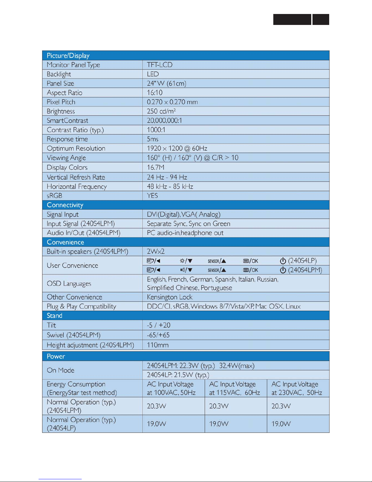
1. Monitor Specifications
Technical specifications
!
!
Meridian 3
6
Note:
1. EPEAT Gold or Silver is valid only where Philips registers the product. Please visit www.epeat.net
for
registration status in your country.
2. This data is subject to change without notice. Go to www.philips.com/support
to download the latest
version of leaflet.
7
Meridian 3
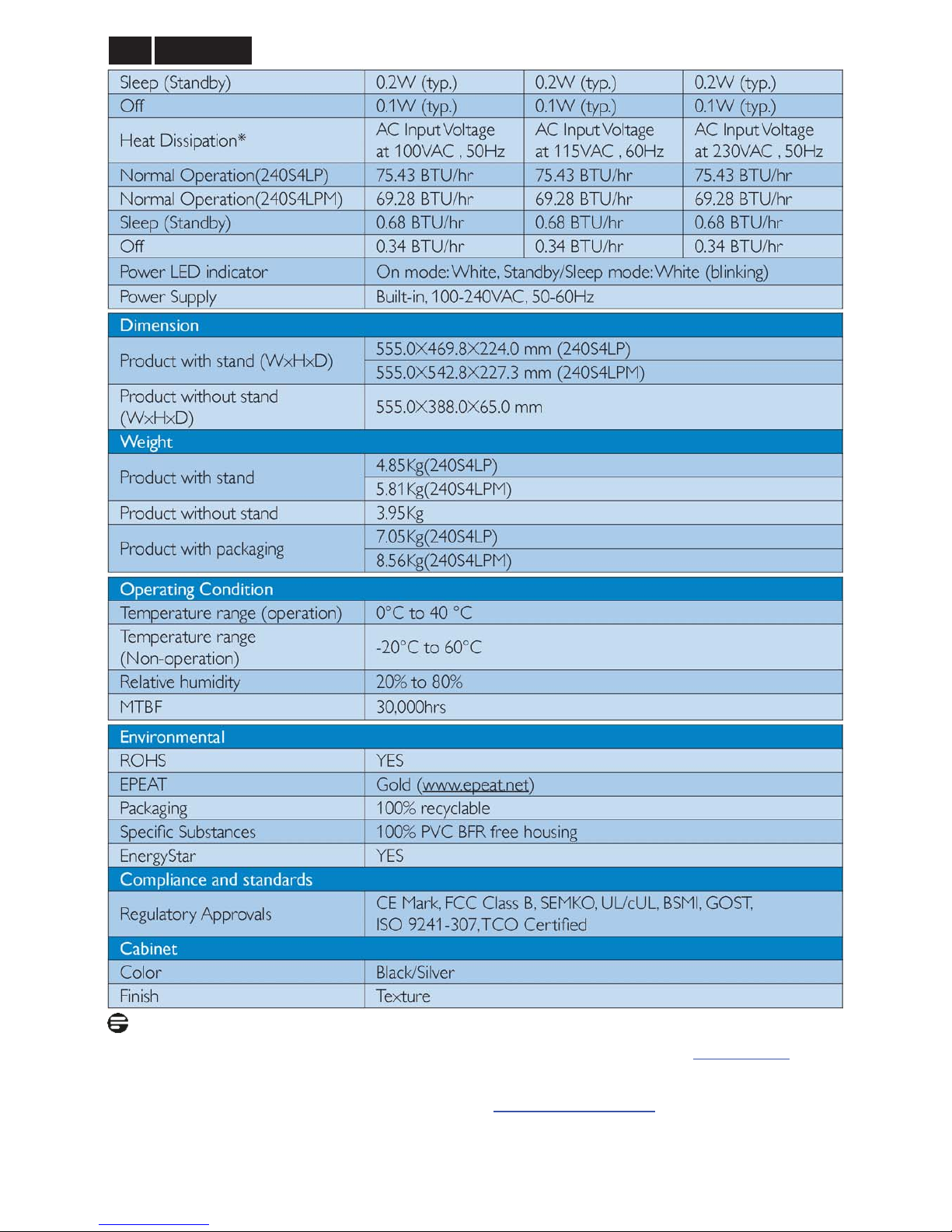
2. LCD Monitor Description
The LCD monitor will contain a scaler board, a power board, a head phone jack board, an IR board and a key
board. The scaler board houses the flat panel control logic, brightn ess control logic and DDC.
The power board will provide AC to DC inverter voltage to drive the backlight of panel and the scaler board chips
each voltage.
Monitor Block Diagram
LED Panel
Scaler Board
LED Drive
IR Board
Video signal, DDC
HOST Computer
AC IN
100 ~ 240 V
Power Board
Key Board Head Phone Jack Board
!
!
Meridian 3
8
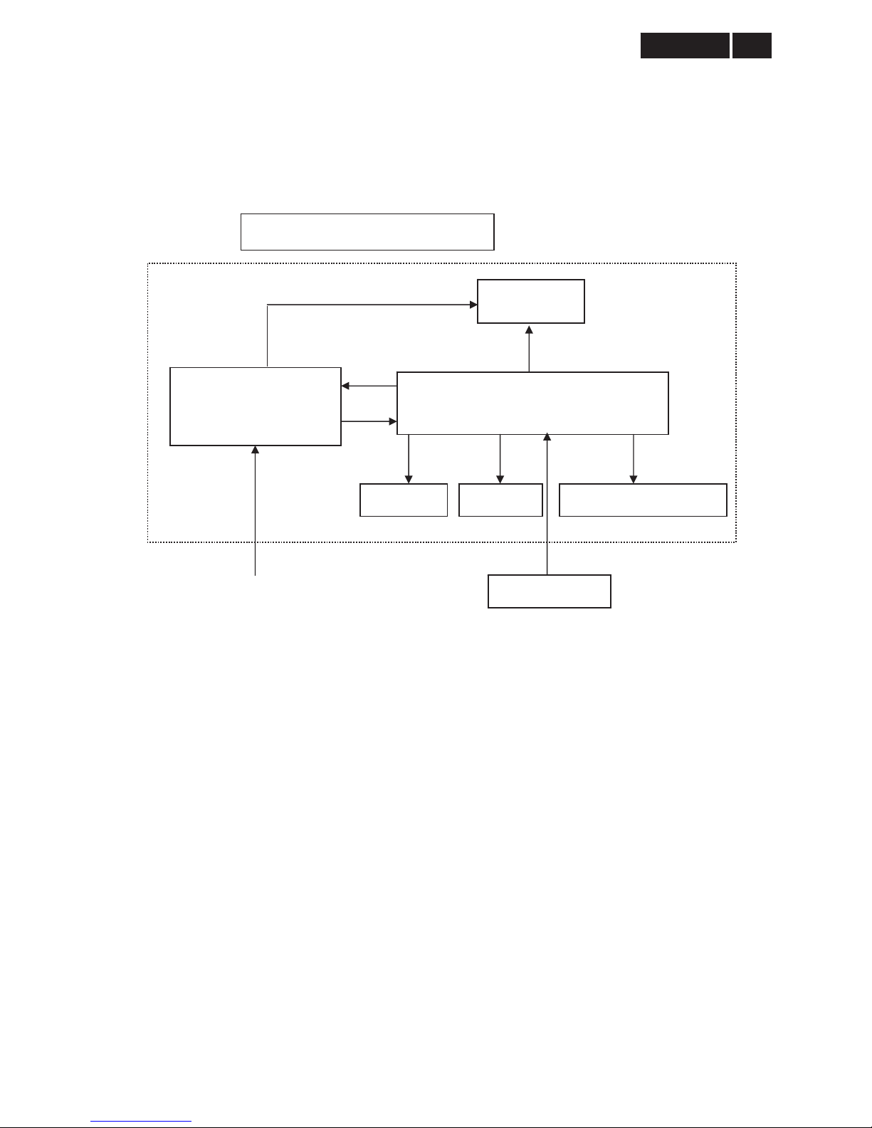
3. Operating Instructions
3.1 General Instructions
Press the power button to turn the monitor on or off.
The other control knobs are located at front panel of
the monitor. By changing these setting, the picture
can be adjusted to your personal preference.
γThe power cord should be connected.
γ Press the power button to turn on the monitor.
The power indicator will light up.
3.2 Control Buttons
Description of the control buttons
Connecting to your PC
1. AC power input
2. DVI input
3. VGA input
4. Kensington anti-theft lock
5. Audio input (Optional)
Connect to PC
1. Connect the power cord to the back of the monitor
firmly.
2. Turn off your computer and unplug its power
cable.
3. Connect the monitor signal cable to the video
connector on the back of your computer.
4. Plug the power cord of your computer and your
monitor into a nearby outlet.
5. Turn on your computer and monito r. If the monitor
displays an image, installation is complete.
9
Meridian 3
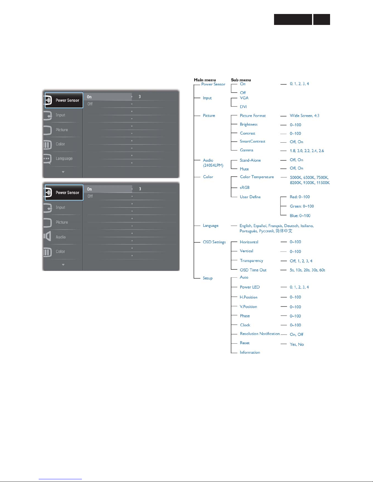
3.3 OSD Menu
On-Screen Display (OSD) is a feature in all Philips
LCD monitors. It allows an end user to adjust screen
performance or select functions of the monitors directly
through an on-screen instruction window. A user
friendly on screen display interface is shown as below:
Basic and simple instruction on the control keys
In the OSD shown above, you can pressźŸ buttons
at the front bezel of the monitor to move the cursor,
and press OK button to confirm the choice or change.
The OSD Menu
Below is an overall view of the structure of the
On-Screen Display. You can use this as a reference
when you want to work your way around the different
adjustments later on.
!
!
Meridian 3
10
4. Input/ Output Specification
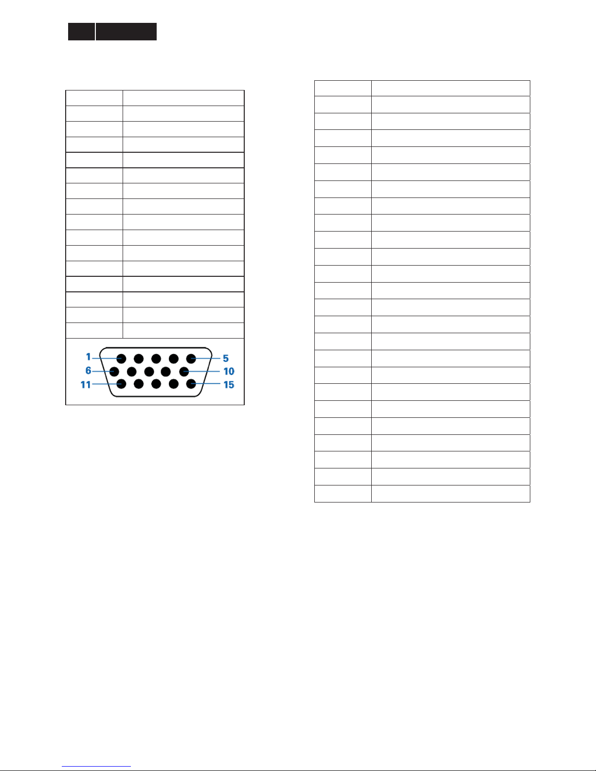
4.1 Input Signal Connector
D-sub Connector
Pin No. Signal Name
1 Red
2 Green/ SOG
3 Blue
4 Sense (GND)
5 Cable Detect (GND)
6 Red GND
7 Green GND
8 Blue GND
9 DDC +3.3V or +5V
10 Logic GND
11 Sense (GND)
12 Bi-directional data
13 H/H+V sync
14 V-sync
15 Data clock
DVI Connector
Pin No. Signal Name
1 T.M.D.S. data22 T.M.D.S. data2+
3 T.M.D.S. data2 shield
4 No Connect
5 No Connect
6 DDC clock
7 DDC data
8 No Connect
9 T.M.D.S. data110 T.M.D.S. data1+
11 T.M.D.S. data1 shield
12 No Connect
13 No Connect
14 +5V Power
15 Ground (for +5V)
16 Hot plug detect
17 T.M.D.S. data018 T.M.D.S. data0+
19 T.M.D.S. data0 shield
20 No Connect
21 No Connect
22 T.M.D.S clock shield
23 T.M.D.S. clock+
24 T.M.D.S. clock-
11
Meridian 3
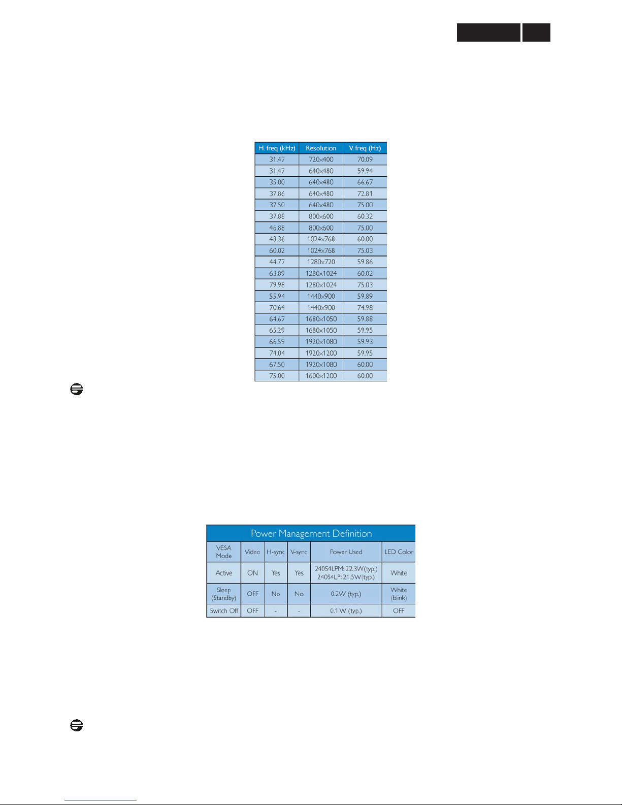
4.2 Resolution & Preset Modes
Maximum Resolution
1920 x 1200 @ 60 Hz (analog input)
1920 x 1200 @ 60 Hz (digital input)
Recommended Resolution
1920 x 1200 @ 60 Hz (digital input)
Note:
Please notice that your display works best at native resolution of 1920 x 1200 @ 60Hz. For best display quality,
please follow this resolution recommendation.
Power Management
If you have VESA DPM compliance disp lay card or software installed in your PC, the monitor can automatically
reduce its power consumption when not in use. If an input from a keyboard, mouse or other input device is detected,
the monitor will 'wake up' automatically. The following table shows the power consumption and signaling of this
automatic power saving feature:
The following setup is used to measure power consumption on this monitor.
• Native resolution: 1920 x 1200
• Contrast: 50%
• Brightness: 250 nits
• Color temperature: 6500k with full white pattern
Note:
This data is subject to change without notice.
!
!
Meridian 3
12
4.3 Pixel Defect Policy
Philips strives to deliver the highest quality products.
We use some of the industry's most advanced
manufacturing processes and practice stringent quality
control. However, pixel or sub pixel defects on the TFT
Monitor panels used in flat panel monitors are
sometimes unavoidable. No manufacturer can
guarantee that all panels will be free from pixel defects,
but Philips guarantees that any monitor with an
unacceptable number of defects will be repaired or
replaced under warranty. This notice explains the
different types of pixel defects and defines acceptable
defect levels for each type. In order to qualify for repair
or replacement under warranty, the number of pixel
defects on a TFT Monitor panel must exceed these
acceptable levels. For example, no more than
0.0004% of the sub pixels on a monitor may be
defective. Furthermore, Philips sets even higher quality
standards for certain types or combinations of pixel
defects that are more noticeable than others. This
policy is valid worldwide.
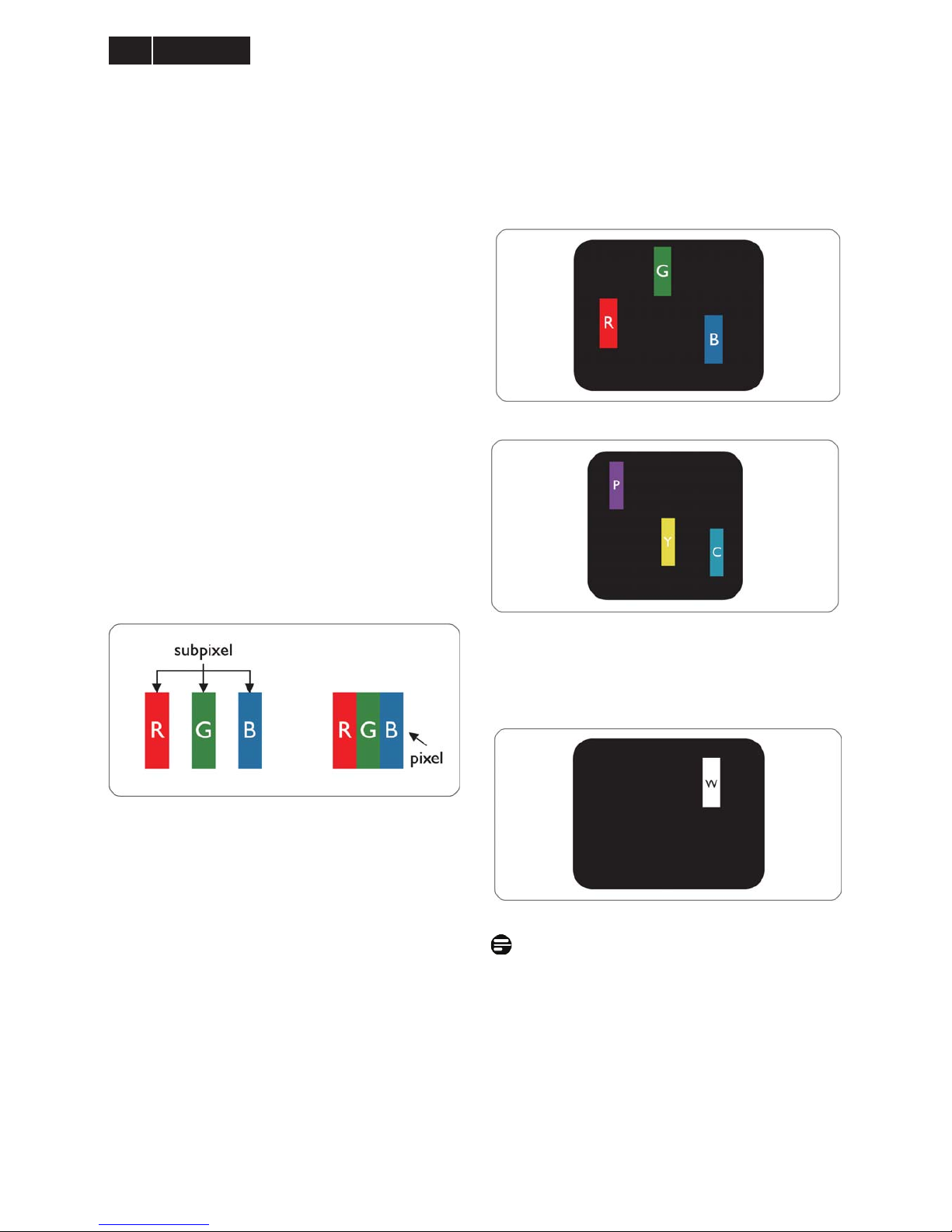
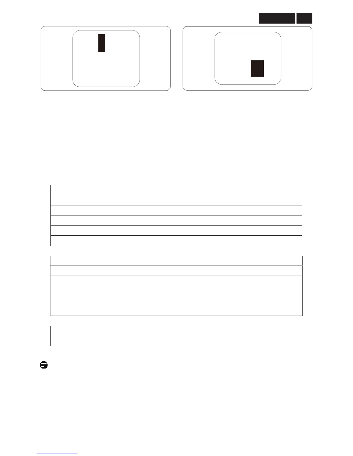
Pixels and Sub pixels
A pixel, or picture element, is composed of three sub
pixels in the primary colors of red, green and blue.
Many pixels together form an image. When all sub
pixels of a pixel are lit, the three colored sub pixels
together appear as a single white pixel. When all are
dark, the three colored sub pixels together appear as a
single black pixel. Other combinations of lit and dark
sub pixels appear as single pixels of other colors.
Types of Pixel Defects
Pixel and sub pixel defects appear on the screen in
different ways. There are two categories of pixel
defects and several types of sub pixel defects within
each category.
Bright Dot Defects
Bright dot defects appear as pixels or sub pixels that
are always lit or 'on'. That is, a bright dot is a sub-pixel
that stands out on the screen when the monitor
displays a dark pattern. There are the types of bright
dot defects.
One lit red, green or blue sub pixel.
Two adjacent lit sub pixels:
- Red + Blue = Purple
- Red + Green = Yellow
- Green + Blue = Cyan (Light Blue)
Three adjacent lit sub pixels (one white pixel)
Note:
A red or blue bright dot must be more than 50 percent
brighter than neighboring dots while a green bright dot
is 30 percent brighter than neighboring dots.
Black Dot Defects Black dot defects appear as pixel s
or sub pixels that are always dark or 'off'. That is, a
dark dot is a sub-pixel that stands out on the screen
when the monitor displays a light pattern. These are
the types of black dot defects.
13
Meridian 3
Proximity of Pixel Defects
Because pixel and sub pixels defects of the same type
that are near to one another may be more noticeable,
Philips also specifies tolerances for the proximity of
pixel defects.
Pixel Defect Tolerances
In order to qualify for repair or replacement due to pixel
defects during the warranty period, a TFT Monitor
panel in a Philips flat panel monitor must have pixel or
sub pixel defects exceeding the tolerances listed in the
following tables.
BRIGHT DOT DEFECTS ACCEPTABLE LEVEL
1 lit subpixel 3
2 adjacent lit subpixels 1
3 adjacent lit subpixels (one white pixel) 0
Distance between two bright dot defects* >15mm
Total bright dot defects of all types 3
BLACK DOT DEFECTS ACCEPTABLE LEVEL
1 dark subpixel 5 or fewer
2 adjacent dark subpixels 2 or fewer
3 adjacent dark subpixels 0
Distance between two black dot defects* >15mm
Total black dot defects of all types 5 or fewer
TOTAL DOT DEFECTS ACCEPTABLE LEVEL
Total bright or black dot defects of all types 5 or fewer
Note:
1. 1 or 2 adjacent sub pixel defects = 1 dot defect
2. This monitor is ISO9241-307 compliant .Class-I compliant.(ISO9241-307: Ergonomic requirement, analysis and
compliance test methods for electronic visual displays)
3. ISO9241-307 is the successor of formerly known ISO13406 standard, which is withdrawn by the International
Organisation for Standardisation (ISO) per: 2008-11-13.
!
!
Meridian 3
14
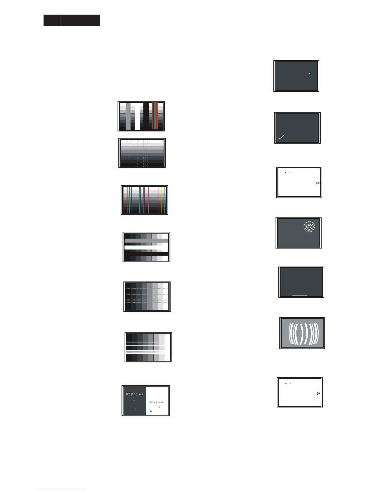
4.4 Failure Mode Of Panel
Failure description
Phenomenon
Vertical block defect
Vertical dim lines
Vertical lines defect
(Always bri
g
ht or dark)
Horizontal block defect
Horizontal dim lines
Horizontal lines defect
(Always bri
g
ht or dark)
Has bri
g
ht or dark pixel
Polarizer has bubbles
Polarizer has bubbles
Foreign material inside
polarizer. It shows liner or
dot shape.
Concentric circle formed
Bottom back light of LCD is
brighter than normal
Back light un-uniformity
Backli
g
ht has foreign material.
Black or white color, liner or
circular type
Quick reference for failure mode of LCD panel
this pa
g
e presents problems that could be made by LCD panel.
It is not necessary to repair circuit board. Simply follow the mechanical
instruction on this manual to eliminate failure by replace LCD panel.
15
Meridian 3
5. Block Diagram
5.1 Scaler Board
PA[0..9]
PB[0..9]
+16V
V33S-DP
+16V
V33S-DP
AUDIO
7. Audio
V5A
Volume
Mute
AIN_R
AIN_L
AOUT_R
AOUT_L
AUDIO_5V
Audio_SD
V5A
USB
8.USB
+16V
DC POW ER SAVI N G
DIS P L AY PO RT
3.DI SPLAY PORT
DP_SINK_ASS_1
DP_SINK_ASS_2
LANE2P
LANE2N
LANE0P
LANE0N
DET_DP
LANE3N
LANE3P
LANE1N
LANE1P
V33S-DP
AUX_CHP
AUX_CHN
DP_HOT_PLUG
INPUT
2.INPUT
RIN
GIN
BIN
VSYNC
GNDR
GNDG
GNDB
HSYNC
SOG
RX0-
RX1+
RX1-
RX2-
RXC-
RX2+
RXC+
RX0+
DVI_SDA
DVI_SCL
DDC_WP
DVI_HPD
DET_DVII
DDCA_SCL
DDCA_SDA
DET_VGAI
SCALER
4.SCALER
V33S
V12S
PB[0..9]
HSYNC
GIN
SOG
VSYNC
GNDG
BIN
GNDR
RIN
GNDB
RX0-
RX2+
RX0+
RX2-
RXC-
RXC+
RX1+
RX1-
on_PANEL
PA[0..9]
on_BACKLIGHT
adj_BACKLIGHT
DET_DP
DVI_HPD
DDC_WP
DET_DVII
DVI_SCL
DVI_SDA
LANE3N
LANE3P
LANE2N
LANE2P
LANE1N
LANE1P
LANE0N
LANE0P
DP_SINK_ASS_1
DP_SINK_ASS_2
AUX_CHP
AUX_CHN
DP_HOT_PLUG
DDCA_SCL
DDCA_SDA
DET_VGAI
Volume
Mute
AIN_R
AIN_L
AOUT_R
AOUT_L
AUDIO_5V
PS_ON
Audio_SD
PANEL12V_ON
DC POW ER SAVI N G
PANEL I NTERF ACE
5.PANEL I N TERF AC E
PB[0..9]
PA[0..9]
VLCD
POWER
6.POW ER
on_PANEL
VLCD
V12S
V33S
V5A
on_BACKLIGHT
adj_BACKLIGHT+16V
V33S-DP
PS_ON
PANEL12V_ON
V12S
V33S
V12S
VLCD
VLCD
V33S
V5A
!
!
Meridian 3
16
5.2 Power Board
16V
EMI filter
Start Re sistor
(R905 R908)
PWM Control
(IC901)
Transformer
AC input
Bridge
Rectifier and
Filter
Feedback Circuit
Rectifier
diodes
Power Switch
(Q901)
Photo coupler
(IC902)
5v
ZD802
LED
(CN802)
IC LED DRIVER
OZ9998AGN-A1-0-TR
(IC801)
16V
ON/OFF
L801
OVP feedback
Current mirror circuit
DIM
17
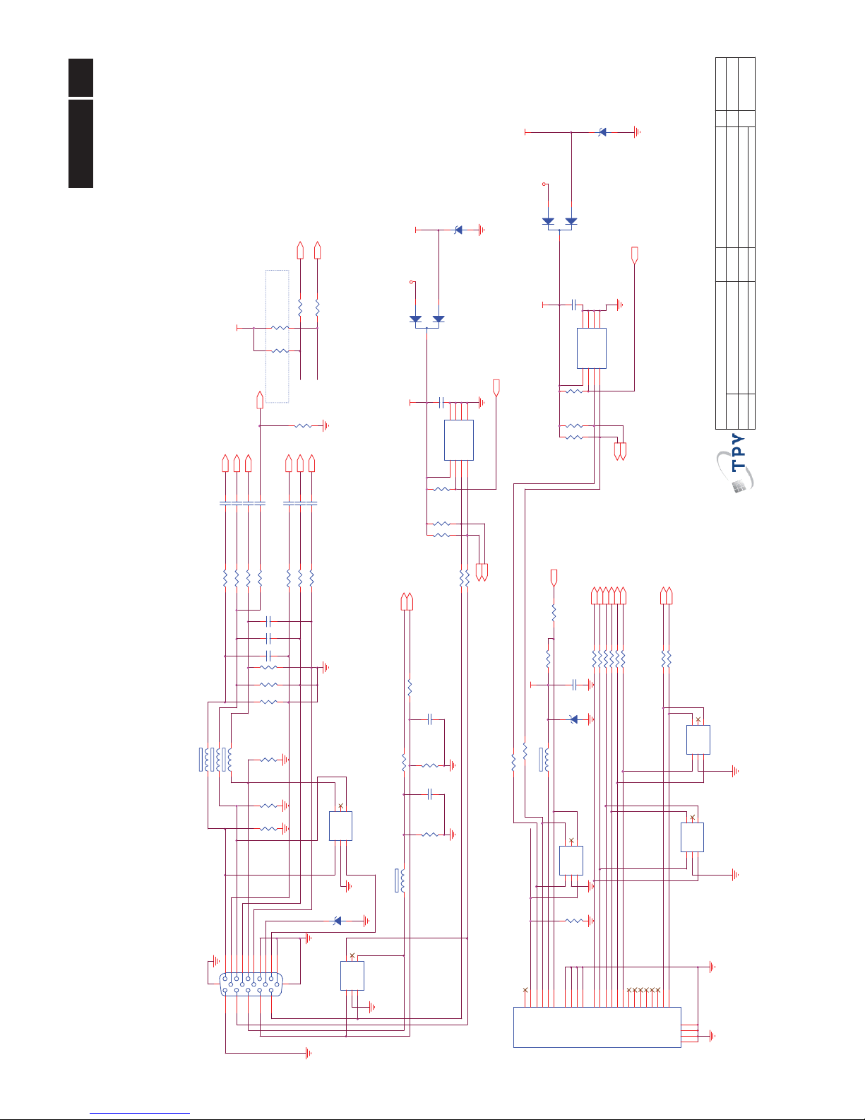
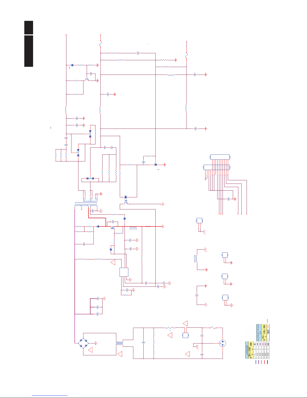
Meridian 3
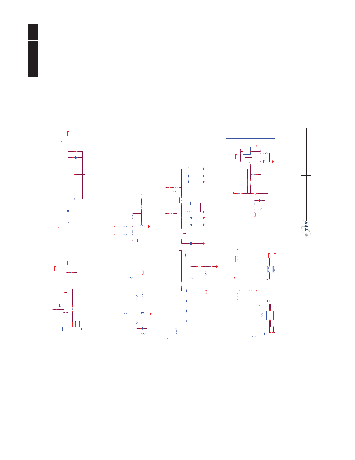
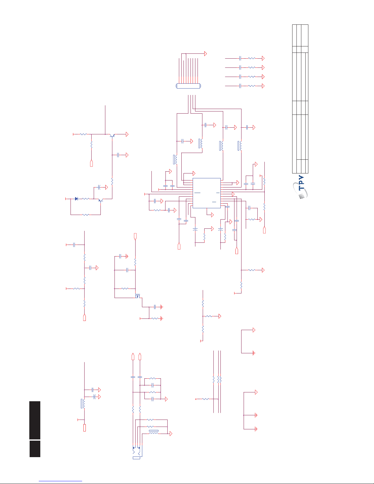
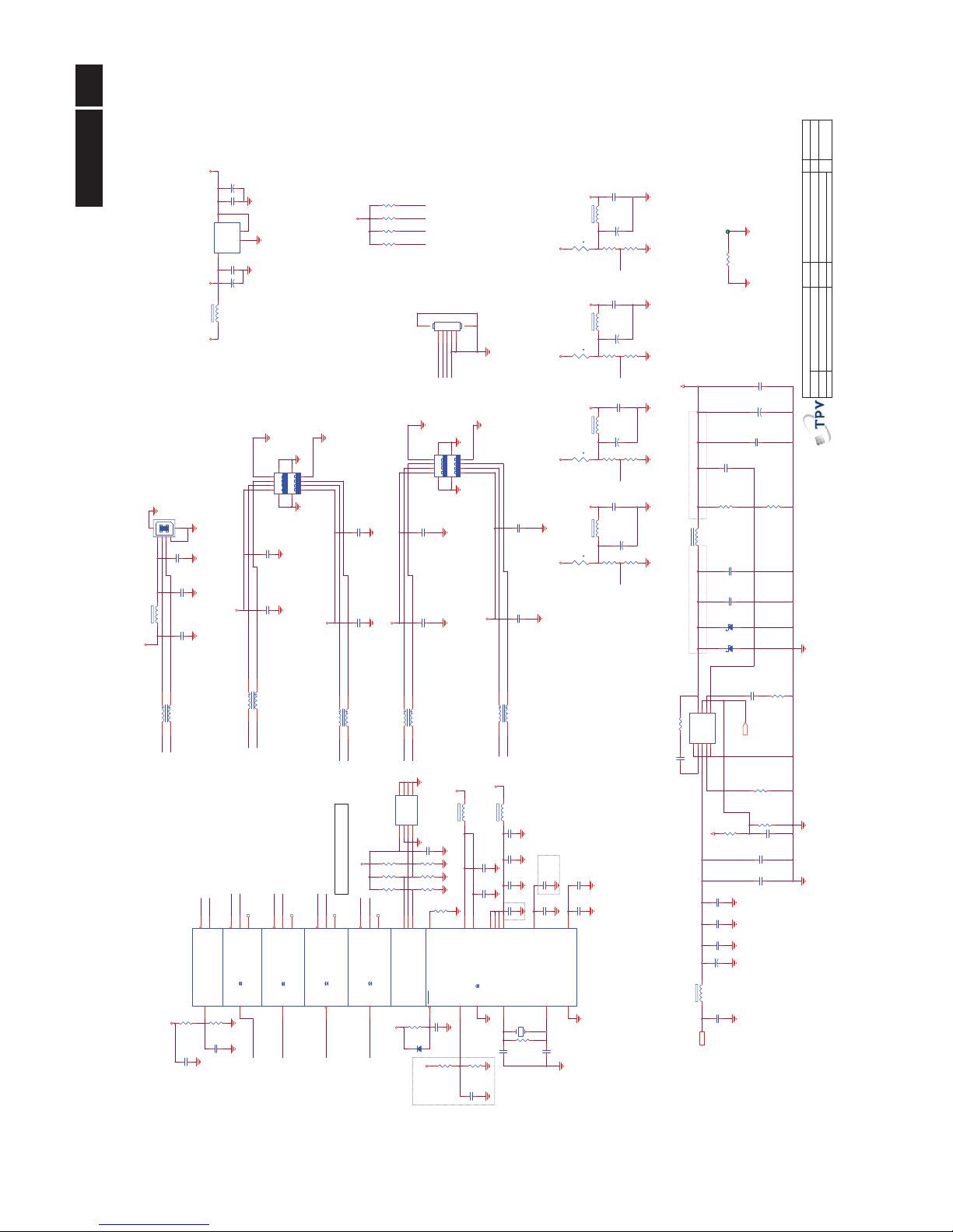
6. Schematic
6.1 Scaler Board (715G5774M01000004K)
Remark: Parts position can be searched by using FIND function in PDF.
ESD_5V
R105 1K C105 22N 25V
V5A
V5A
D102
BAT54C
3
1
2
DAT1-
DDC_WP
DVI5V
DAT1+
DAT0-
SCL_VGA
C102 47N16VR102 22 OHM 1/16W
R133 10 OHM
R135 10 OHM
RED-
R138 10 OHM
GREEN-
BLUE-
R111 100OHM
R137 10 OHM
R10675R 1/ 16W 1%
R110 100OHM
R141 10 OHM
ZD102
RLZ5.6B
1 2
HPD
R140 10 OHM
R136 10 OHM
R114 100OHM
DET_VGA
SCL_DVI
R134 10 OHM
DET_DVI
RIN 5
GNDR 5
VSYNC 5
BIN 5
GIN 5
R112
NC/1M 1/ 16W 5%
R139 120R 0.3A
12
DET_VGAI 5
HSYNC 5
GNDB 5
GNDG 5
R115 100OHM
SOG 5
RX1- 5
RX0- 5
RX1+ 5
DVI_SDA5
DDCA_SCL5
DDCA_SDA5
RX2+ 5
RX0+ 5
RXC- 5
RXC+ 5
DVI5V
VGA5V
RED+
DVI_SCL5
DDC_WP 5
DDC_WP 5
HSI
U101
CAT2 4C02W I-GT3A
A01A12A2
3
GND
4
SDA5SCL6WP7VCC
8
U103
CAT24C02WI-GT3A
A01A12A2
3
GND
4
SDA5SCL6WP7VCC
8
DET_DVI
C118
220N 10V
R122
4.7K1/16W
C116
220N 10V
RX2- 5
DAT0+
GREEN+
R121 4.7K1/16W
R120 4.7K1/16W
R124 47R 1/16W 5%
R130 4.7K1/16W
R123 47R 1/16W 5%
R131 4.7K1/16W
DDC_WP
U109
AZC398-04S
I/O11GND2I/O2
3
I/O3
4
NC
5
I/O4
6
R119
2.2K1/16W
R118
2.2K1/16W
R116 100OHM
C1075P F 50V
C1085P F 50V
DAT2-
DAT2+
C1065P F 50V
R113 100OHM
ZD101
RLZ5.6B
1 2
R109
NC/22K 1/ 16W 5%
R108
NC/22K 1/ 16W 5%
VSI
DCLK+
DCLK-
FB101 19R 0.5A
1 2
FB103 19R 0.5A
1 2
FB102 19R 0.5A
1 2
FB104 120R
R127 1K
CN101
DB15
162738495
1112131415
10
1716
DET_DVII 5
R129
NC
R125 47R 1/16W 5%
DET_VGA
SDA_DVI
ESD_VGA
VGA5V
D101
BAT54C
3
1
2
CN102
JACK
DAT2-
1
DAT2+
2
2/4shield
3
DAT4-
4
DAT4+
5
DDC SCL
6
DDC SDA
7
VSYNC
8
DAT1-
9
DAT1+
10
1/3shield
11
DAT3-
12
DAT3+
13
+5V
14
SYNC GND
15
HPD
16
DAT0-
17
DAT0+
18
0/5shield
19
DAT5-
20
DAT5+
21
clk shield
22
clk+
23
clk-
24
GND
26
GND
25
GND
27
GND
28
U110
AZC398-04S
I/O11GND2I/O2
3
I/O3
4
NC
5
I/O4
6
U102
AZC398-04S
I/O11GND2I/O2
3
I/O3
4
NC
5
I/O4
6
U104
AZC398-04S
I/O11GND2I/O2
3
I/O3
4
NC
5
I/O4
6
U105
AZC398-04S
I/O11GND2I/O2
3
I/O3
4
NC
5
I/O4
6
ZD103
NC/R LZ5.6B
ZD104
NC/R LZ5.6B
C115
22P 50V
ESD_DVI
C117
100N 16V
SDA_VGA
R128
NC/4K7 1/ 16W 5%
DVI_HPD 5
OEM MODEL
Size
Rev
Date
Sheet
of
TPV MOD EL
PCB NAME
〠⡩
T P V ( Top Victory Electronics Co . , Ltd. )
Key Component
㎜䳄⬌㎚㞩
B
Custom
39Monday, Oc t ober 08, 2012
〠⡩
<>
G5774-M0B-000-0040-1-120713
R101
75R 1/16W 1%
R10775R 1/16W 1%
R103 22 OHM 1/16W
R104 22 OHM 1/16W
R163
NC/75R 1/16W 1%
R162
NC/75R 1/16W 1%
R164
NC/75R 1/16W 1%
C114
22P 50V
BLUE+
R126 47R 1/16W 5%
R132
4.7K1/16W
C103 47N16V
C104 47N16V
C109 47N16V
C110 47N16V
C111 47N16V
ESD_5V
ESD_5V
R117 100OHM1/16W
INPUT
!
18
Meridian 3
Remark: Parts position can be searched by using FIND function in PDF.
R159
1K
DP_SINK_ASS_2 5
DP_SINK_ASS_1 5
U108
AZC398-04S
I/O11GND2I/O2
3
I/O3
4
NC
5
I/O4
6
R165
100K1/16W
R161
NC/ 10K 1/16W 5%
R167 0R05 1/16W
R168 0R05 1/16W
DP_VDD
need to layer
Differential Trace
CN103
DP CONN
SHELL1
21
SHELL2
22
ML_ Lane 3(n)
1
GND
2
ML_ Lane 3(p)3ML_ Lane 2(n)
4
GND
5
ML_ Lane 2(p)6ML_ Lane 1(n)
7
GND
8
ML_ Lane 1(p)9ML_ Lane 0(n)
10
GND
11
ML_ Lane 0(p)
12
GND13GND
14
AUX_CH(p)
15
GND
16
AUX_CH(n)
17
Hot Plug Detect
18
Return
19
SHELL4
24
SHELL3
23
DP_PWR
20
R156 0R05 OH M
DP_VDD
AUX_CHP 5
AUX_CHN 5
DP_HOT_PLUG 5
AUX_CHP
DP_VDD
ZD105
NC/RLZ5.6B
1 2
DP_VDD
LANE3P
LANE3N
LANE2P
LANE2N
LANE1P
LANE1N
LANE0N
LANE0P
R151
1M 1/16W
R152
NC
AUX_CHN
R154 0R05 OH M
t
F101
PTCR
1 2
V33S-DP7
U107
AOZ8804DI
CH11CH22VN3CH34CH4
5
NC6NC
7
VN
8
NC9NC
10
LANE0P
LANE0N
LANE1P
LANE1N
LANE2N
LANE2PLANE2P
LANE3P
LANE3N
DP_VDD
R166
NC/0R 05 1/ 16W
OEM MO D EL
Size
Rev
Date
Sheet
of
TPV MOD EL
PCB NAME
〠⡩
T P V ( Top Victory Electronics Co . , Ltd. )
Key Component
㎜䳄⬌㎚㞩
B
B
49Monday, Oc t ober 08, 2012
〠⡩
<>
DP INPUT
U106
AOZ8804DI
CH11CH22VN3CH34CH4
5
NC6NC
7
VN
8
NC9NC
10
C122
100N 16V
R153 1K
R157
NC
R158
1M 1/16W
DET_DP 5
R150 100OHM
LANE2N
LANE2P
LANE0P
LANE3N
LANE0N
LANE3P
LANE1P
LANE1N
LANE0P 5
LANE0N 5
LANE3P 5
LANE3N 5
LANE1P
LANE0N
LANE1N
LANE0P
LANE2N 5
LANE1N 5
LANE2P 5
LANE1P 5
LANE3P
LANE2P
LANE3N
LANE2N
C120
100N 16V
DISPLAY PORT
19
Meridian 3
Remark: Parts position can be searched by using FIND function in PDF.
R436 0R05 OHM
CN402,CN403 BOTH LAYOUT
Pin 118
PW ON Latch:
Internal MCU :Pull High
External MCU :Pull Low
POWER
C443
10UF 10V
V12C
V33SDRAM
R482 100OHM
WP_PRO
DDC_WP 3
R439
NC/22K 1/16W 5%
C404
100N 16V
R418
4.7K1/16W
on_BACKLIGHT7
+
C423
NC/10UF50V
+
C418
100UF 16V
PS_ON7
PWM4
CN401
CONN
12345
DVI_HPD3
AOUT_R1
V33TMDS
Adj_BACKLIGHT7
CN402
CONN
1234567891011
12
PANEL12V_ON7
DP_HOT_PLUG4
X401
14.31818MHZ/32PF
12
R422 NC
R423 NC
C420 1uF 10V
KEY2
LED_1
AUDIO_5V8
LED_2
V33TMDS
CN403
NC/CONN
12345
6
R430 100OHM
V33SDRAM
AOUT_L1
R431 100OHM
V33LSADC
R425
10K
V33CRYSTAL
KEY1
KEY2
FB407 120R
PA0
PA1
V12ADC
PA2
R416 560R 1/16W 5%
Mute 8
Mute
PA3
+
C403
100UF 16V
R435
0R05 OHM
PA4
R437
0R05 OHM
C427
NC/1N 50V
FB401 120R
DVI_SDA3
DVI_SCL3
PA6
PA5
PA7
R408 0R05 OHM
R407 0R05 OHM
R417
NC/1M 1/16W 5%
PS_DISTANCE
FB406 120R
DET_DP 4
PA8
PA9
DET_DP
PB0
PB1
PB2
R411
NC
C409
220N 10V
R412
10K
PB3
VCC3.3
WP
SDOUTCESDIN
R41522R 1/16W 5%
R41422R 1/16W 5%
R41322R 1/16W 5%
R440
47K 1/16W 5%
PB4
PB5
GNDG 3
SOG 3
GNDR 3
RIN 3
HSYNC 3
GIN 3
GNDB 3
BIN 3
VSYNC 3
+
C417
NC/100UF 16V
Audio_SD 8
XO
PB6
PB7
PB9
PB8
R404
4K7 1/16W 5%
R424
10K
LED driver
C401
220N 10V
R402 4.7K1/16W
C428
NC/1N 50V
R403 4.7K1/16W
PA[0..9] 6
V33P
TO Processor Board
PB[0..9]6
CLK
RX2+ 3
RX1+ 3
RX2- 3
RX0- 3
C440
10UF 10V
RX1- 3
RXC- 3
RX0+ 3
RXC+ 3
C441
100N 16V
VCC3.3
PIVOT_EN
VCC3.3
OC_SW
R455
100R 1/10W 5%
Q466
LMBT3904LT1G
C435100N 16V
OC401
RBS311115
4 3
1 2
R453
10K 1/16W 5%
R456
4.7K1/16W
Q402
LMBT3906LT1G
R445
NC/10K
WP_PRO
R474
NC
C442
100N 16V
C434100N 16V
ZD401
RLZ5.6B
1 2
LED_A
R444 N C/100OHM
LED_A
R463
NC
R447NC
LED_1
R473
56 OHM +-5% 1/8W
LED_2
R490
0R05 OHM
R443 N C/100OHM
R472
0R05 OHM
V5A
C410
NC/10pF 16V
V5A
LANE1P4
LANE3P4
R406
0R05 OHM
C421
100N 16V
LANE0P4
LANE2N4
LANE0N4
LANE2P4
LANE1N4
WP
LANE3N4
DET_DVII
DET_VGAI
DET_DP
ZD402
RLZ5.6B
1 2
R467
10K
R448NC
C433NC
C407 100N 1 6V
AUX_CHP4
C430
NC
EESCLEE_SCL
R4503.9K1/16W
R410 1K
R465
NC
C432NC
EESDAEE_SDA
R464
NC
C431NC
Q401
LMBT3906LT1G
R470
NC
R471
NC
R462 0R05 OHM
R460
10K
R4513.9K1/16W
R446
NC/10K
R426 0R 0 5 OH M
DDCA_SDA 3
R469
22K1/16W
R427 0R 0 5 OH M
DDCA_SCL 3
ZD403
RLZ5.6B
1 2
R4523.9K1/16W
R466
1 OHM +-5% 1/8W
R475
0R05OHM1/8W
R461
22K1/16W
R449NC
R468
NC
PWM1
PWM2
R486 0R05 OHM
C438100N 16V
C419100N 16V
VCC3.3
VCC3.3
VCC3.3
VCC3.3
AOUT_L1
C406 100N 1 6V
AUX_CHN4
AOUT_R1
AIN_R 8
AIN_L 8
AOUT_L 8
AOUT_R 8
R420
6.2KOHM 5% 1/16W
R405
100OHM
DP_SINK_ASS_ 2 4
ERGO_ON
FB408
120R
12
R401
100OHM
UART_TXD
UART_RXD
P53
ERGO_ON
PS_OUTPUT
PS_DISTANCE
R421
NC
P52
OEM MODEL
Size
Rev
Date
Sheet
of
TPV MODEL
PCB NAME
〠⡩
T P V ( Top Victory Electronics Co . , Ltd. )
Key Component
㎜䳄⬌㎚㞩
B
Custom
59Monday, October 08, 2012
〠⡩
<>
SCALER RTD24 86TD
LED_G
LED_A
+
C422
100UF 16V
C416
100N 16V
DDCA_SCL 3
DDCA_SDA 3
C425
100N 16V
R433 NC
R434 NC
+
C408
NC/10UF16V
U403
M24C16
A01A12A2
3
GND
4
SDA5SCL6WP7VCC
8
U402
MX25L4006EM1I-12G
CE#
1
SO
2
WP#
3
GND
4
VDD8HOLD#7SCK6SI
5
VCC3.3
R409
4.7K1/16W
P53
+
C424
NC/10UF50V
P52
R457100K1/16W
C439
NC/1N 50V
C426
NC/1N 50V
EESCL
VCC3.3
EESDA
Near to scalar
DET_VGAI
R441
47K 1/16W 5%
DET_VGAI 3
DET_DVII 3
DET_DVII
R442
47K 1/16W 5%
VCC3.3
VCC3.3
VCC3.3
on_Panel7
POWER
LED_G
C414
100N 16V
V5A
V5A
V5A
R432
NC/10K 1/16W 5%
U401
RTD2486T D-GR
DP_VDD/TMDS_VDD
1
TMDS_REXT
2
LANE0P/RX2 P_0
3
LANE0N/RX2N_0
4
LANE1P/RX1 P_0
5
LANE1N/RX1N_0
6
LANE2P/RX0 P_0
7
LANE2N/RX0N_0
8
LANE3P/RXCP_0
9
LANE3N/RXCN_0
10
DP_GND/TMDS_GND
11
LANE0P/RX2 P_1
12
LANE0N/RX2N_1
13
LANE1P/RX1 P_1
14
LANE1N/RX1N_1
15
LANE2P/RX0 P_1
16
LANE2N/RX0N_1
17
LANE3P/RXCP_1
18
LANE3N/RXCN_1
19
DP_VDD/TMDS_VDD2
20
AVS0
21
AHS0
22
ADC_VDD
23
B0-
24
B0+
25
G0-
26
G0+
27
SOG0
28
R0-
29
R0+
30
GPI/GPO/V8_7
31
GPI/GPO / V8_6
32
ADC_GND
38
GPI/GPO/V8_1
37
GPI/GPO/V8_2
36
GPI/GPO / V8_3
35
GPI/GPO / V8_4
34
GPI/GPO/ V8_5
33
AUDIO_SOUTL/ V8_3/SCK/G PIO
45
SPDIF3/AUDIO_REF/V8_4/WS/GPIO
44
A-ADC0/VCL K/GPIO
50
A-ADC1/GPIO51A-ADC2/GPIO52A-ADC3/GPIO53A-ADC4/GPIO
54
TCON[0][5]/BADC0/PWM1/PWM5/GPIO
55
TCON[1][4]/B-ADC1/IICSCL/GPIO
56
V8_7/GPIO
41
TCON[9][1 1]/B-ADC2 /IICSD A/GPIO
57
TCON[7][10]/DDCSCL1/GPIO
58
TCON[3][5]/DDCSDA1/GPIO
59
VCCK
60
PGND
61
PVCC
62
TCON[1][8]/PWM2/GPIO
63
SD0/SPDIF0/TCON[0][7]/GPIO/IrDA
64
AUDIO_HOUTL/V8_1/S D0/GPIO
47
AUDIO_HOUTR/V8 _0/PWM0/GPIO
48
ABLU7/SCK/TCON[4][2]/GPIO/BB3N
66
ABLU6/MCK/TCON[5][9]/GPIO/BB2P
67
ABLU5/SD0/SPDIF0/TCON[13][3]/GPIO/BB2N
68
LINE_INL/V8_6/ IICSCL/GPIO
42
ABLU4/SPDIF1/SD1/TCON[ 7][3]/GPIO/IICSCL/BB1P
69
ABLU3/SPDIF2/SD2/TCON[ 9][11]/GPIO/IICSDA/BB1N
70
ABLU2/SPDIF3/SD3/TCON[10][8]/GPIO/PWM1/PWM5/BCLKP
71
TCON[6][12]/GPIO/PWM3/BCLKN
72
VCCK
73
ABLU1/ GPIO/ABLU7/ T XO3+_8b/TXO4+_10b/BG3P
74
ABLU0/ GPIO/ABLU6/ TXO3-_ 8b/T XO4- _10b/ BG3N
75
AGRN7/GPIO/ABLU 5/TXOC+_8b/TXO3+_10b/ BG2P
76
AGRN6/GPIO/ABLU4 /TXOC-_8b/TXO3-_10b/ BG2N
77
AUDIO_SOUTR/V8_2/MCK/GPIO
46
PVCC
84
PGND
85
ARED7/AGRN3/TXE3+_8b/TXO0+_10b/BR1P
86
LINE_INR/V8_5/ IICSDA/GPI O
43
GPIO/PWM3/TCON[11][6]/TXE0-_10b/AG2N
99
GPIOVCLK
40
LS_ADC_VDD
49
MCK/TCON[7]/GPIO/ AR1P
108
GPIO/V8_0/
39
XO
127XI128
WS/TCON[7][1]/GPIO/PWM1/BB3P
65
AGRN5/GPIO/ABLU 3/TXO2+_8b/TXOC+_10b/ BG1P
78
AGRN4/GPI O/ABLU2/TX O2-_8b/TXOC -_10b/BG1N
79
AGRN3/GPIO/AGR N7/TXO1+_8b/TXO2+_10b/B R3P
80
AGRN2/GPIO/AGR N6/TXO1-_8b/TXO2-_10b/ BR3N
81
AGRN1/GPIO/AGR N5/TXO0+_8b/TXO1+_10b/B R2P
82
AGRN0/GPIO/AGR N4/TXO0-_8b/TXO1-_10b/ BR2N
83
ARED6/AGRN2/ TXE3-_8b/TXO0-_10b/BR 1N
87
ARED5/ARED7/ TXEC+_8b/TXE4+_10b/AB3P
88
ARED4/ARE D6/TXEC-_ 8b/TXE4+_10b/ AB3N
89
ARED3/ARED5/TXE2+_8b/TXE3+_10b/AB2P
90
ARED2/ARED4/TXE2-_8b/TXE3-_10b/AB2N
91
ARED1/ARED3/ TXE1+_8b/TXEC+_10b/AB1P
92
ARED0/ARED2/ TXE1-_8b/TXEC-_10b/ AB1N
93
DENA/TXE0+_8b/T XE2+_10b/ACLKP
94
DHS/TXE0-_8b/T XE2-_10b/ACLKN
95
DCLK/GPIO /PWM0/T XE1+_10b/AG3P
96
DVS/GPIO/PWM1/TXE1-_10b/AG3N
97
GPIO/PWM2/TXE0+_10b/ AG2P
98
GPIO/PWM4/TCON[12][3]/AG1P
100
GPIO/PWM5/TCON[0]/AG1N
101
SD3/ SPDIF3/TCON[10]/GPIO/PWM0/AR3P
102
SD2/SPDIF2/TCON[8]/GPIO/I ICSCL/PWM1/AR3N
103
SD1/SPDIF1/TCON[5]/GPIO/IRQ/IICSDA/AR2P
104
SD0 / SPDIF0 / TCON[9] / GPIO / AR2N
105
PVCC
106
PGND
107
SCK/TCON[3]/GPIO/AR1N
109
WS/TCON[6 ]/GPIO/SD T
110
SD0/SPDIF0/TCON[4]/GPIO/SPDI F1
111
SD1/ SPDIF1/TCON[9]/GPIO/WS
112
SD2/SPDIF2/TCON[1][11]/GPIO/IrDA/SCK
113
SD3/SPDIF3/TCON[13]/GPIO/VCLK/MCK
114
SPI_SCLK/SeriesDat a
115
SI/MCU_SCLK
116
SO/SCSB
117
CEB/IRQB
118
GPIO/PWM5/SPDIF1
119
VCCK
120
DDCSCL3/GPIO/AUX-CH_P1
121
DDCSDA3/GPIO/AUX-CH_N1
122
DDCSCL2/GPIO/AUX-CH_P0
124
DDCSDA2/GPIO/AUX-CH_N0
123
RESETB
125
CEC/GPIO/PWM1/SPDIF2
126
E-Pad
129
V33SDRAM
OC_SW
SDOUT
CLKCESDIN
PIVOT_EN
on_Panel
R458
10K
CE
V33CRYSTAL
DP_SINK_ASS_ 1 4
V33TMDS
V12C
R428 N C
R429 N C
DC POWER SAVING9
XI
Volume
V33P
XO
Volume 8
PS_OUTPUT
UART_TXD
UART_RXD
C405
100N 16V
KEY1
KEY2
For Auto Pivot Function
C411
22P 50V
R438
NC/22K 1/16W 5%
V12S7
V12CV12S
V33S7
VCC3.3 V33P
R419
NC/4K7 1/16W 5%
V12ADC
C412
22P 50V
V12C
V33LSADC
KEY1
ERGO_ON
FB402 120R
V33P
FB405 120R
FB403 120R
V33P
FB404 120R
XI
SCALER
!
20
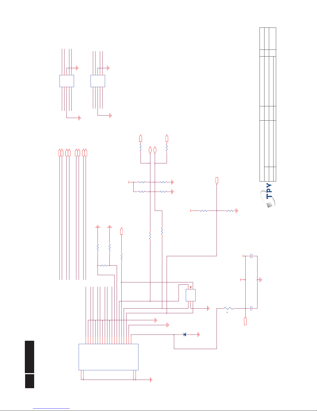
Meridian 3
Remark: Parts position can be searched by using FIND function in PDF.
C437
100N 16V
C429,C431 lay
ǂ
LVB1PPB6
LVB2MPB5
LVB1MPB7
LVB3MPB1
LVB3PPB0
LVBCKPPB2
LVBCKMPB3
LVB2PPB4
PB[0..9]
FB409
120R 6A
1 2
R4811.5K 1/4W
CN408
CONN
24681012141618202224262830
13579
111315171921232527
29
CN407
NC/CONN
123456789
101112131415161718192021222324252627282930
LVB0PPB8
LVB0MPB9
RXO0- RXO0+
RXO1- RXO1+
R4801.5K 1/4W
RXO2-
PA6 LVA1P
PA5 LVA2M
RXO2+
PA0 LVA3P
PA4 LVA2P
PA3 LVACKM
PA1 LVA3M
PA7 LVA1M
PA[0..9]
RXOC-
PA8 LVA0P
RXOC+
RXO3- RXO3+
RXE0-
PB[0..9]5PA[0..9]5
RXE0+
VLCD 7
VLCD
RXE1- RXE1+
RXE2- RXE2+
RXEC- RXEC+
option
RXE3- RXE3+
OEM MODEL
Size
Rev
Date
Sheet
of
TPV MO D E L
PCB NAME
〠⡩
T P V ( Top Victory Elec t ronic s C o . , Lt d. )
Key Component
㎜䳄⬌㎚㞩
B
A
69Monday, Oc t ober 08, 2012
〠⡩
<>
PANEL INTERFACE
PA9 LVA0M
LVA0P RXE0+
PA2 LVACKP
RXE3-LVA3M
RXO3-LVB3M
RXE2-LVA2M
RXE1-LVA1M
LVB2M RXO2-
RXO1-LVB1M
RXO0-LVB0M
LVACKM RXEC-
LVBCKM RXOC-
RXE0-LVA0M
RXOC+LVBCKP
RXO0+LVB0P
RXE2+LVA2P
RXO1+LVB1P
RXEC+LVACKP
RXO3+LVB3P
RXO2+LVB2P
RXE1+LVA1P
RXE3+LVA3P
+
C436
150UF 25V
PANEL INTERFACE
21
Meridian 3
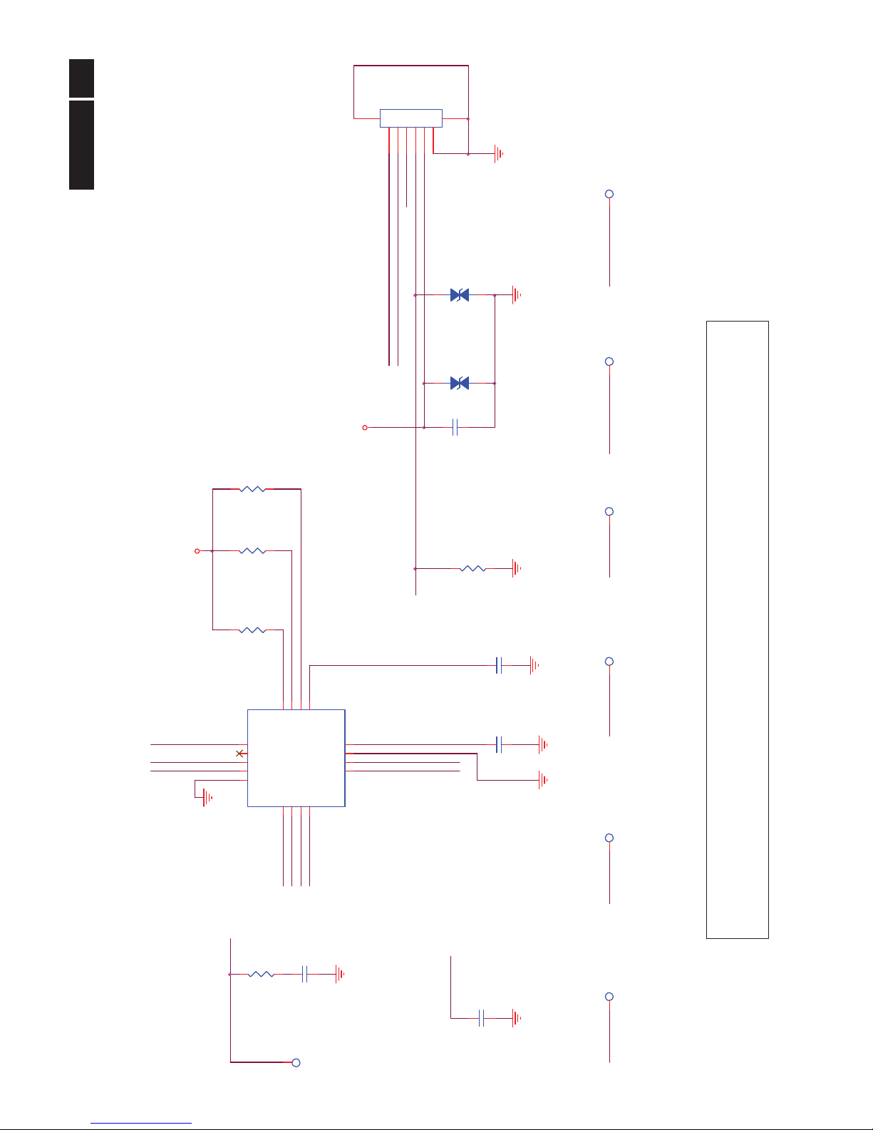
Remark: Parts position can be searched by using FIND function in PDF.
Scaler Core
Adj_BACKLIGHT 5
on_BACKLIGHT 5
PANEL12V_ON5
V5A
V5A R731
10K
BKLT_EN
C726
10N 50V
FB702
120R 6A
L702
2.2uH
FB704
120R 6A
R721
10K 1/10W 5%
R724
4K7 1/10W 5%
FB703
120R 6A
R717
12.1K 1%
R715
4.7K1/16W
+16V
C720
10UF 25V
C724
100NF 25V
V5A
C714
100NF 25V
D703
SX36
1 2
R720
0R05 OHM
C715
1uF 25V
R722
10 OHM
C719
22P 50V
+
C727
220UF 16V
R723
14.7KOHM 1/10W
+
C730
150UF 25V
R728 24K 1/16W 5%
U703
AT1528P11U
VCC1REF2GND3FB
4
EN
5
PGND
6
LX
7
VIN
8
R726
10K
C713
100NF 25V
R714
30Kohm 1/16W +/-5%
Q705
NC/AO3401
C718
22P 50V
Q704
LMBT3904LT1G
C723
100NF 25V
C716
1uF 25V
C728
100N 16V
C729
0.47uF 16V
C725
10UF 10V
C712
10UF 25V
D705
NC/LL4148
+
C722
150UF 25V
R727
10K
VLCD
VLCD 6
on_Panel5
R716
10K
H: OnL:Off
C721
10UF 25V
TCON POWER
+3.3V_SW
+3.3V
GND
GND
GND
C711
10UF 25V
Q706
AO4411
S
1
S
2
S
3
G
4
D
8
D
7
D
6
D
5
+3.3V_SW
+
C710
150UF 25V
R729
NC/47K 1/16W 5%
FB701
48R 6A
1 2
C717
820pF 50V
R730
10K
D704
SX36
1 2
R713 NC/ 100K1/16W
U702
APW7089KAI-TRG
VIN1EN2UGND3VCC
4
LX
5
COMP
6
FB
7
GND
8
LX
9
GND
GND
R719
62K1/16W
+12V_Panel
+12V_Panel
+12V_Panel
L701
10uH 20%
BKLT_ADJ
R718
63.4K 1%
AT1528P11U: Max:2A
Vout = 0.8V (1+(ĴR1/R2 ))
Cancel U705
V33S
V33S 5
V33S-DP 4
+16V
R701
100R 1/10W 5%
PS_ON1
BKLT_ADJ
R703
10K 1/10W 5%
+
C701
150UF 25V
BKLT_EN
R706
NC/0R05 OHM
OEM MODEL
Size
Rev
Date
Sheet
of
TPV MODE L
PCB NAME
〠⡩
T P V ( Top Victory Electronics Co . , Ltd. )
Key Component
㎜䳄⬌㎚㞩
A
Custom
79Monday, October 08, 2012
〠⡩
<>
07.POWER 1A1D2H1D
U701
TJ3940GRS-1.2
VOUT
2
VIN
3
GND
1
CN701
CONN
1234567891011
12
D701
SR34H
1 2
D702
SR34H
1 2
V5A 3,5,8
V5A
+16V 9
+
C703
220UF 16V
C702
1N 50V
(1)LGD LM240WU8-SLD1 (12V):
R717=10K;R718=140K
(2)SEC LTM240CL01(5V):
R717=12.1K;R718=63.4K
need to adj 3.3V
R702
10K 1/10W 5%
R705
220ohm 1/16W +/-1%
V33S
R709
NC
R712
0R05 1/10W
PS_ON 5
C707
100N 16V
C705
100N 16V
+
C706
100UF 16V
R708
10K 1/10W 5%
R704
NC
R710
100OHM
R711
0R05 OHM
C708
100N 16V
Q701
LMBT3904LT1G
R709->0ohm
R701->0ohm
R706 ->100ohm
Q1 NC
Q702
NC/LMBT3904LT1G
C709
100P 50V
+
C704
100UF 16V
R707 22K1/16W
V12S 5
GND
V33S
V12S
V33S
V33S V5A
POWER
!
22
Meridian 3
Remark: Parts position can be searched by using FIND function in PDF.
C608
100N 16V
OUT-L-
Earphone_Det
Headset _R
OUT-R+
VCC_IN
Headset _L
OUT-R-
OUT-L+
OEM MOD EL
Size
Rev
Date
Sheet
of
TPV MODEL
PCB NAME
〠⡩
T P V ( Top Victory Electronics Co . , Ltd. )
Key Component
㎜䳄⬌㎚㞩
A
Custom
89Monday, October 08, 2012
〠⡩
<>
09.AUDI O APA2 606
R614
10K
AA4
Q601
AO3401A
OUTR
OUTL
FB606 120R 6A
1 2
C605330PF 50V
R628
100OHM
C623 NC
R603
10K
SE-1
Q602
LMBT3906LT 1G
1
23
C618
0.47uF 16V
R627
0R05 OHM
+
C612
100UF 16V
SE
R632
NC
R607
10K
R624
33K 1/16W
C604 1UF 16V
FB601
120R 6A
1 2
C616
10UF 10V
R606
1K
FB602
120R 6A
12
C626
1UF 16V
R619 150R 1/10W 5%
C622
1UF 16V
R626
0R05 OHM
+
C601
220UF 16V
C602
100N 16V
R64033K 1/16W
R618
100K1/16W
Heat Sink = Q90G6119 4
R605
10K
R601
100OHM
C619
NC
Q603
LMBT3904LT1G
C624
0.47uF 16V
C625
100N 16V
C631
220PF 50V
R602
10K
R611
10K
R621 150R 1/10W 5%
R609
10K
R610
10K
C603 1UF 16V
R613 0R05 1/10W
R631
0R05 1/10W
R608
470OHM1/16W
FB605 120R 6A
1 2
+
C620
220UF 16V
R630
NC
C628
220PF 50V
+
C621
220UF 16V
FB603 120R 6A
1 2
R620 100K1/16W
R623
1K
R629
100OHM
CN601
PHONE JAC K
12354
R625
NC
R612 0R05 1/10W
C617
1UF 16V
C610
1UF 16V
R616
1K
C630
220PF 50V
R622
3K1/16W
D601
LL4148
C615
1UF 16V
R64133K 1/16W
C614
1UF 16V
C629
220PF 50V
C627
10UF 10V
C613
100N 16V
C606330PF 50V
FB604 120R 6A
1 2
U601
APA2606NAI-TRG
LOUTP
1
PGND
2
PGND
3
LOUTN
4
PVDD
5
MUTE
6
VDD
7
LINN
8
UVP
9
VDC
10
VOLUME
11
HP_LOUT
12
HP_ROUT
13
BYPASS
14
SE/BTL
15
AGC
16
RINN
17
GND
18
SD
19
PVDD
20
ROUTN
21
PGND
22
PGND
23
ROUTP
24
Thern al P a d
25
V5A3,5,7
+5V_AUDIO
+5V_AUDIO
+5V_AUDIO
+5V_AUDIO
+5V_AUDIO
V5A
+5V_AUDIO
+5V_AUDIO
+5V_AUDIO
+5V_AUDIO
+5V_AUDIO
C607
100N 16V
Headset_L
C609
100N 16V
Headset_R
Earphone_Det
Mute5
AOUT_L5
AIN_L 5
AOUT_R5
AIN_R 5
OUT-R+
CN602
CONN
123456789
MUTE-1
OUT-L-
G-2
OUT-R-
UVP
G3
OUT-L+
AUDIO_5V
VCC_IN
MUTE- 1
G-1
Volume5
AUDIO_5V 5
UVP
C632
NC/330 pF 50 V
R633
NC/10 OHM
AA1
VOL
OUTR
SE
C633
NC/33 0pF 50 V
R634
NC/10 OHM
Audio_SD5
C634
NC/330 pF 50 V
R636
NC/10 OHM
R635
NC/10 OHM
C635
NC/33 0pF 50 V
AA2
AA3
AA4
MUTE
AA1
R617
100OHM
R604
10K
C611
100N 16V
VOL
+5V_AUDIO
MUTE-1
AA2
OUTL
AA3
AUDIO
23
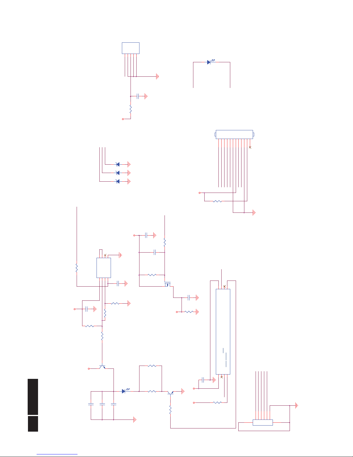
Meridian 3
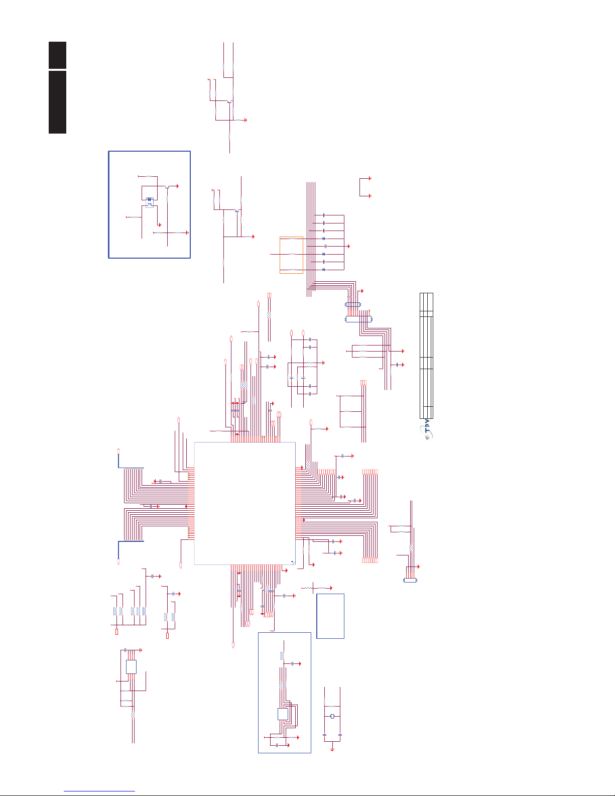
Remark: Parts position can be searched by using FIND function in PDF.
/OC2
/OC1
DP2
DM2
/OC1
VBUS1A
DM44
C542
1N 50V
C539
1N 50V
UGND
UGND
FB507
120R 0.3A
1 2
/OC3
VBUS_DET
C528
1N 50V
C529
1N 50V
UGNDUGND
2A
/OC2
Power Regulator
CN501
CONN
12345
67
Layout Note
C530
100N 16V
DP0
Disable Downstream 4
VBUS0
UGND
12
34
CN504
CONN
123
4
6 5
DM / DP pa i r to p ai r
б
35mil
DM0
UGND
DM4
UGND
DP4
U802 Decoupling
ㆯ⭗ى㏬
IC
б
DM / DP :7
mils
DM / DP Trace
䭓
à
ǂǂ
70
ǂ
DM / DP Trac e widt h 18 mi l s
Disable Downstream 3: R735, R736 pull high 10K
Disable Downstream 4: R737, R738 pull high 10K
UGNDUGND
EEPROM mount: R812~814 pull hi
MP1584EN
U501
SW
1
EN
2
COMP
3
FB
4
GND5FREQ6VIN7BST8Thermal P a d
9
/OC3
DC POWER SAVING5
EEPROM NC: R818~820 p ull low
UGND
DM11
DP4
DP11DP1
DP44
DM1
DP3
DM3
DM4
1B
1A
1234
5678
CN503
USB CONN
1
2
3
4
6
5
7
8
11
12
9
10
DM1
DP1
DM2
DP2
VBUS2A
DM33
DP3
UGND
VBUS3
C535
100N 16V
L503
90R/400mA
1
2
4
3
UGND
DM3
DP33
VBUS3A
C536
1N 50V
UGND
R735
0R05
/OC4
C532
1N 50V
UGND
UGND
/OC4
VBUS4A
VBUS4
+16V7
DP44
DM44
UGND
DM2
UGND
DP2
L504
90R/400mA
1
2
4
3
VBUS2
DM22
C534
1N 50V
C533
100N 16V
UGND
DP22
UGND
C538
1N 50V
OEM MOD E L
Size
Rev
Date
Sheet
of
TPV MOD E L
PCB NAME
〠⡩
T P V ( Top Victory Electronics Co . , Ltd. )
Key Component
㎜䳄⬌㎚㞩
C
A2
99Monday, Oc t ober 08, 2012
〠⡩
<>
11.USB2.0 _U SB 251 4
UGND
C504
10uF 25V
UGND
DP0
DM1
UGND
C505
10uF 25V
DP1
R507
10K
C503
10uF 25V
R505
68.1K 1%
R515
0R05 1/10W
+
C520
100UF 16V
C510
150pF 50V
R504
100K1/16W
R532
10K
R514
15K 1/16W
R522
100K1/16W
C526
100N 16V
FB505
120R 6A
1 2
FB501
120R 6A
1 2
C540
1uF 10V
R506
12.4K 1%
R526
11.5K +-1% 1/16W
C544
33P 50V
U503
NC/M24C02-WMN6TP
A01A12A2
3
GND
4
SDA5SCL6WP7VCC
8
D504
NC/LL4148
C517
100N 16V
C507
0.1uF 50V
C548
4.7UF
D502
SR34H
1 2
C586
1N 50V
C531
100N 16V
Ups tr eam
Dow n st re am 1
Dow n st re am 2
Dow n st re am 3
Dow n st re am 4
EEPROM/ Con f ig
Common
U502 US B2514B-AEZC
USBUP_DP
31
USBUP_DM
30
USBDN1_DP
2
USBDN2_DP
4
USBDN3_DP
7
USBDN4_DP
9
USBDN1_DM
1
USBDN2_DM
3
USBDN3_DM
6
USBDN4_DM
8
VBUS_DET
27
PRTPWR1
12
PRTPWR2
16
PRTPWR3
18
PRTPWR4
20
OCS_N[1]
13
OCS_N[2]
17
OCS_N[3]
19
OCS_N[4]
21
RBIAS
35
SDA/SMBDATA/N ON_REM1
22
SCL/SMBCLK/ CFG_SEL0
24
HS_IND/CFG_SEL1
25
XTAL1/CLKIN
33
XTAL2/CLKIN_EN
32
RESET26LOCAL_PWR/NON_REM0/SUSP_IND28TEST
11
VDD33
23
PLLFILT
34
VDDA33
29
VDDA33/VDD33PLL
36
VDD33
15
CRFILT
14
VSS(FLAG)
37
VDDA335VDDA33
10
FB502
120R 6A
1 2
C519
100N 16V
+
C524
100UF 16V
FB509
120R 6A
1 2
t
F503
PTCR
12
C511
1N 50V
C537
100N 16V
R517
NC/10K
C554
100N 16V
C513
10uF 25V
t
F502
PTCR
12
C509
100N 16V
U504
AP1117E33L-13-77
ADJ(GND)
1
VOUT
2
VIN
3
4
4
L506
90R/400mA
1
2
4
3
R524
10K
R508
15K 1/16W
R531
NC
L501
22uH
R520
51K 1/16W 5%
R519
NC/10K
R512
15K 1/16W
R511
10K
C547
100N 16V
R523
NC
C501
0.1uF 50V
C550
100N 16V
R501
10K 1/10W 5%
C555
NC
C551
100N 16V
R527
NC
FB503
120R 6A
1 2
DM0
C545
100N 16V
R513
10K
C506
0.1uF 50V
C512
1N 50V
X501
24.000MHZ
12
FB506
120R 6A
1 2
R530
10K
C508
0.1uF 50V
R518
NC/10K
C553
100N 16V
C521
100N 16V
R503
300K
+
C522
100UF 16V
+
C502
150UF 35V
FB508
120R 6A
1 2
C549
4.7UF
+
C514
470uF 10V
+
C518
100UF 16V
t
F504
PTCR
12
R525
1M 1/16W
D501
SR34H
1 2
C541
100N 16V
+
C527
100UF 16V
C543
33P 50V
R510
15K 1/16W
C546
4.7UF
R509
10K
R528
10K
R521
100K1/16W
+
C516
100UF 16V
R502
30K 1/10W 5%
t
F501
PTCR
12
R516
NC/10K
C525
100N 16V
R529
NC
C523
100N 16V
C515
100N 16V
FB504
120R 6A
1 2
C552
100N 16V
UGND
VBUS0
UGND UGND
UGNDUGND
UGND
U5V
L505
90R/400mA
1
2
4
3
VBUS1
UGND
UGND
UGND UGND
UGND
UGND
UGND
UGND
U5V
VBUS4
USB3.3V
UGND
UGND
UGND
UGND
VBUS0
UGND
VBUS4
UGND
UGND
UGND
UGND
UGND
USB3.3V
USB3.3V
VBUS2
UGND
UGND
USB3.3V
USB5V
USB3.3V
USB5V
VBUS3
UGND
UGND
UGNDUGND
L502
90R/400mA
1
2
4
3
UGND
UGND
UGND
UGND
UGND
UGND
USB5V
USB3.3V
UGND
UGND
UGND
UGND
UGND
VBUS1
USB5V USB5V
USB3.3V
UGNDUGND
UGND
1234
5678
CN502
USB CONN
1
2
3
4
6
5
7
8
11
12
9
10
UGND
UGND
UGND
2010/1/25
USB
!
24
Meridian 3
6.2 Power Board (715G5164P02002001M)
Remark: Parts position can be searched by using FIND function in PDF.
IC801
OZ9998AGN
PWM1ISEN12ISEN23ISEN34ISEN45GNDA6ISEN87ISEN68ISEN79OVP10ISET11RT
12
ENA
13
ISW
14
ISEN5
15
LDR
16
VREF
17
GNDP
18
VIN
19
SEL
20
COMP
21
SSTCMP
22
NC
23
STATUS
24
R851
0R05 1/10W
FB802
BEAD
1 2
CN803
NC
12345
R847
0R05 1/10W
R849
NC
+
C813
100uF
Q801
EMBA2N10A
R806
10K 1/10W 5%
Vout
R812
100R 1/10W 5%
C805
0.47uF 16V
R808
NC
R810
1K 1/10W 5%
C807
2U2 16V
JUMP/EMI
R824
47KOHM +-1% 1/10W
ZD801
NC/SK510B
R804 27K 1/10W 1%
R809
100K
C806
0.47UF 50V
C811
100PF 50V
R805
270K +-1% 1/8W
+16V
CN802
NC
12345
6
7 8
R801
0.3R 1/ 4W
FB803
BEAD
1 2
IS1
IS3
IS2
IS7
IS6
IS4
C812
100P 50V
R814
10R
IS8
IS5
L801
33UH
2
4
IS1
IS2
IS3
R848
1R 1/10W 5%
IS4 IS8IS7IS5 IS6
R850
1R 1/10W 5%
R852
1R 1/10W 5%
+
C804
4.7UF 100V
IO1 IO3IO2 IO4
R846
1R 1/10W 5%
C820
0.47UF 50V
C821
0.47UF 50V
FB801
NC
1 2
IO1
IO2
IO3
IO4
ZD802
SR5100
R844
10 OHM 1/4W
R822
1M 1/8W 5%
C815
330NF 16V
Vout
Vout
R842
RST 0603 18K 1% 1/10W
R845
100 OHM 1/4W
C814
680P 50V
CN801
CONN
246
135
R802
0.3R 1/ 4W
R813 10K 1/10W 5%
C801
0.1uF 50V
DIM
ON/OFF
OVP1
OVP1
R807
10R 1/10W 5%
IO2
IO1
IO3
IO4
Vout
CONVERTER
25
Meridian 3
Remark: Parts position can be searched by using FIND function in PDF.
C919
1000PF 50V
IC901
LD7750RGR
OTP1COMP2CS3GND
4
OUT
5
VCC
6
HV
8
C934
1N 50V
C922
1N 50V
L904
3.5uH
R917
220oHM
CN902
CONN
123456789
10
R932
100KOHM +-5% 1/8W
R908
10 K 1/4W
D902
FR107
D904
1N4148
C911
0.1uF 50V
R910
1 OHM 1/4W
R919
0.39R
C914
NC
C924
100N 50V
C906
1500PF2KV
R905
10 K 1/4W
R923
22 OHM 1/4W
F903
T4AL 250V
NC/F902
T4AL 250V
C921
330PF 500V
+
C905
100uF 450V
IC903
TL431G-A-TA
R913
100K
R914
100K
R907
100K
R906
100K
R927
10KOHM +- 1% 1/8W
+5V
+16V
+5V
Q903
KTD1028
CN901
SOCKET
12
3
R962 47 OH M 1/4W
Audio_SD
R920
47 OHM 1/4W
FB902
BEAD
1 2
+5V1
!
T901
POWER X''FMR
54632
789
10
11
12
C910
2N2 500V
C929
2N2 500V
C935
2N2 500V
HV
R939
1K 1/8W
!
L903
3.5uH
F901
T4AL 250V
C931
100N 50V
C903
470NF
+
C913
47UF 50V
5V/2.5A
16V/2.35A
+
C915
470UF 16V
R943
470OHM +-5% 1/8W
C932
1N 50V
NC/D907
SFF1004G
1
2
3
R925
2.2 KOHM + -1% 1/8W
+
C916
1000UF 10V
HS2
HEAT SINK(D 905)
1
2
HS3
HEAT SINK(D 906)
1
2
C907
NC
R940
1K OHM
ZD902
GDZJ24B
C912
2N2 500V
D905
MBRF10100CT
1
2
3
C933
47nF 50V
R947
820R
R946
820R
-
+
BD901
KBJ408G
2
1
3
4
C920
47PF1KV
CN905
CONN
L
1
N
2
NC/C930
100N 50V
D906
MBRF20200CT
1
2
3
NC/R933
20KOHM +-1% 1/8W
HS1
HEAT SINK
1
2
C901
0.001uF/2 50V
R902
680K 1/4W
DIM
+16V
NC/L905
3.5uH
GND
GND
1
2
C902
0.001uF/250 V
!
ON/OFF
IC902
PS2561DL1-1
12
43
R924
820 OHM 1/4W
L901
30MH
1
2
4
3
!
R961 47 OH M 1/4W
R935 47 OH M 1/4W
+
C917
470UF 35V
C900
0.0022uF/ 250V
+
C905A
NC
VOL
R918
47 OHM 1/4W
R916
47 OHM 1/4W
R903
680K 1/4W
R926
2K 1/8W 1%
L906
NC
+
C918
470UF 35V
t
NR901
NTCR
12
R930
9K53 1/8W 1%
NC/C N903
CONN
123456789
1011121314
FB901
BEAD
1 2
MUTE
R901
680K 1/4W
R912
10K 1/4W
R911
22 OHM 1/4W
Q901
SMK0870F
!
D903
FR107
POWER
!
26
Meridian 3
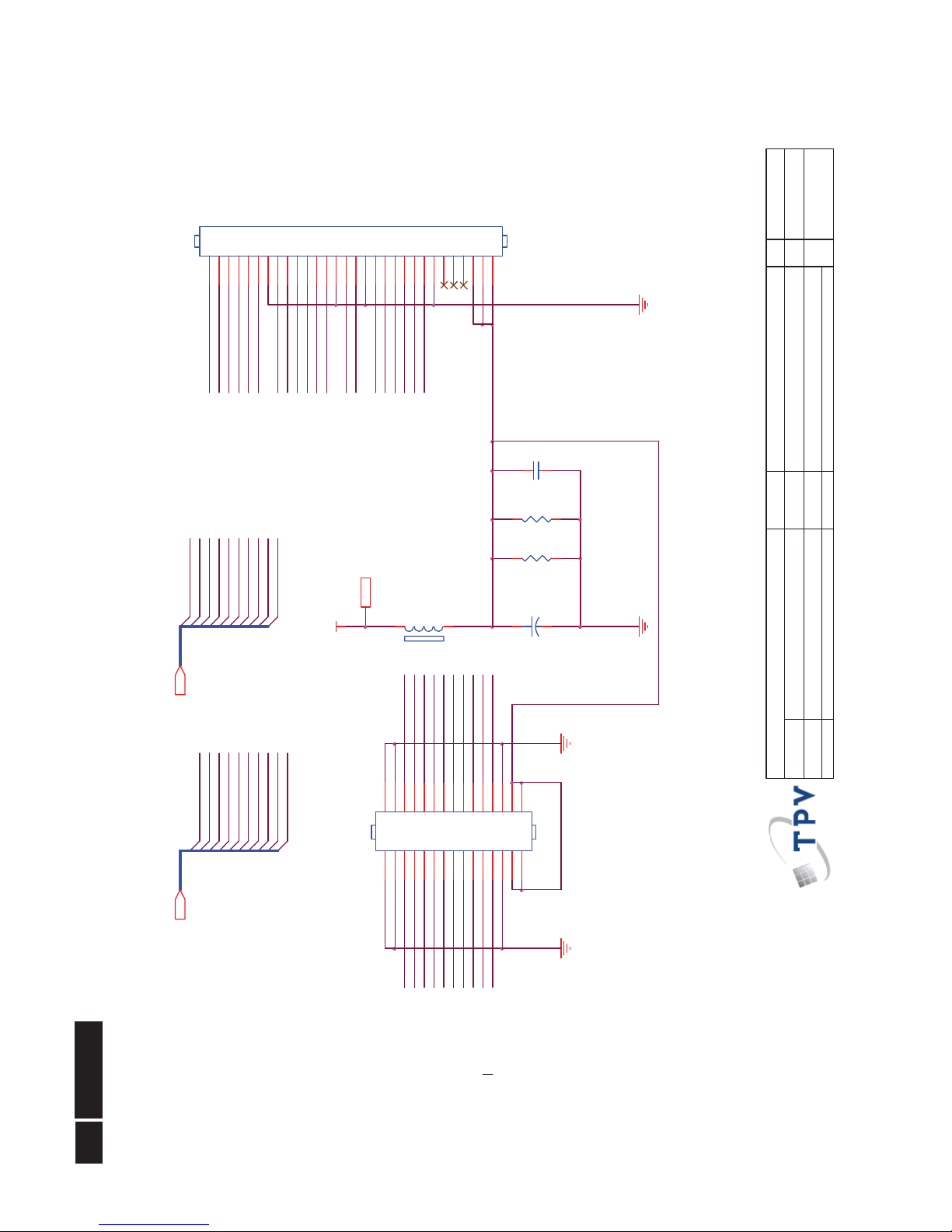
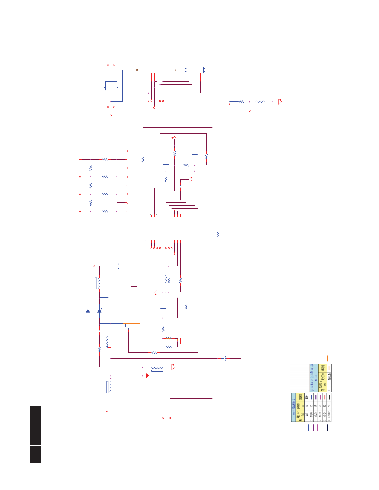
6.3 IR Board (715G5459R01000004S)
Remark: Parts position can be searched by using FIND function in PDF.
IR_RX
PS_OUTPUT
VCC_IN
IR_RX
R/A: 081G 15W 1 EL
V/T: 081G 63W 2 GP
REVERSE: 081G 14 31 EL
FFC R/A: 311GF100C06ADH
FFC V/T: 311GF100D06ACJ
FFC CABLE: 089G 76J 6 3
WIRE V/T: 033G8032 6F S HR
FFC R/A: 311GF100C12ADH
FFC V/T: 311GF100D12ACJ
FFC CABLE: 395G076J12NM01
WIRE V/T: 033G803212F S HR
R313
NC/1K
C311
NC/100N 16V
C318
NC/ 100N 16 V
C316
NC/100N 16V
C312
NC/ 100 N 16V
C317
NC/100N 16V
R312
NC/100K1/16W
LED_VCC
PS_OUTPUT
C315
NC/100N 16V
CN311
CONN
12345
6
78
VCC_KB
R323
NC/10K
I2C_SDA
PS_ON
ZD312NC/UDZSNP5.6B
1 2
CN312
CONN
123456789
101112
PS_DISTANCE
I2C_SCL
SM_INT#
R315
NC/100K1/16W
C314 NC/22UF 16V
R320
NC/100OHM
R316
NC/100 OH M 1/8W
R311
NC/1K
U311
NC/AS358MTR-E1
1OUT
1
1IN-
2
1IN+
3
GND
4
2IN+52IN-62OUT7VCC+
8
R317
NC/33 OHM 1/8W
U313
NC/PIC12F615-I/SN
VDD1GP5/T1CKI/P1A*/OSC1/CLKIN2GP4/AN3/CIN1-/T1G/P1B*/OSC2/CLKOUT3GP3/T1G*/MCLR/VPP
4
GP2/AN2/T0CKI/INT/COUT/CCP1/P1A
5
GP1/AN1/CIN0-/VREF/ICSPCLK
6
GP0/AN0/CIN+/P1B/ICSPDAT
7
VSS
8
C313 NC / 22U F 16V
ZD313NC/UDZSNP5.6B
1 2
R319
NC/1K
Q313
NC/AO3401A
C320
NC/100N 16V
R324
10K
R322
NC/10K
C319
NC/ 100N 16 V
Q312
NC/SST2222A
R314
NC/100K1/16W
U312
NC/IRM-3638M3S28
VOUT1GND2VCC3HAND14HAND2
5
R321
NC/1K
LED311
A8824B/IR204C-A
12
LED312
LED
12
ZD311NC/UDZSNP5.6B
1 2
R318
NC/ 33 OH M 1/ 8W
Q311
NC/SST2222A
VCC
VCCVCC
VCC_IN
VCC
VCC
VCC
VCC_IN
PS_ON
VCC_KB
LED_White
I2C_SCL
I2C_SDA
PS_ON
PS_OUTPUT
PS_DISTANCE
LED_VCC
PS_DISTANCE
LED_white
SM_INT#
POWER SENSOR_LED
27
Meridian 3
6.4 Key Board (715G5446K01000004S)
Remark: Parts position can be searched by using FIND function in PDF.
SM_INT#
CIN_07
FFC R/A: 311GF100C06ADH
FFC V/T: 311GF100D06ACJ
FFC CABLE: 089G 76J 6 3
WIRE V/T: 033G8032 6F S HR
CIN_07
CIN_11
CIN_03
V3.3
R003
4.7K1/16W
R005
100OHM
R004
680OHM +-5% 1/10W
C004
100P 50V
MenuBrightness PowerSmartPower
GPIO_00
C003
100N 16V
CIN_01
SmartPowerBrightness
TP6 KEY0.1524
Menu
CIN_05
C001
100N 16V
Differential
C002
100N 16V
SmartImage
GPIO_00
SM_CLK
U001
IT7230EFN/BX
CIN031CIN072CIN093CIN11
4
VSHILD
5
VBIAS
6
AVSS
7
AVCC
8
DVCC
9
SCLK
10
SDA
11
INT#
12
GPIO0
13
GPIO1
14
CIN00
15
CIN01
16
E-PAD
17
ZD001
MLVS0603M04
12
CIN_09
SmartImage
CIN_03
SM_DATA
SM_INT#CIN_05
V3.3
V3.3
AC_SHIELD
VBIAS
Power
R001
10K
AC_SHIELD
CIN_01 CIN_09CIN_11
KEY0.1524
TP3
KEY0.1524
TP2
KEY0.1524
TP5
KEY0.1524
TP1
R002
4.7K1/16W
KEY0.1524
TP4
CN001
CONN
12345
6
78
KEY0.1524
TP7
VBIAS
ZD002
MLVS0603M04
12
SM_CLK CLK
C005
1UF 16V
V3.3
DATASM_DATA
KEY-TOUCHPAD_NONE LED
 Loading...