

Philips 240P4QPYEB/00, 240P4QPYES/00, 240P4QPYNS/93, 240P4QPYNB/00, 240P4QPYNB/69 Service Manual
...
24ƎLCD Color Monitor Chassis: Meridian 3
Service
Service
Service
Description
Page
Table of Contents.........................................………….1
Revision List………….................................................2
Important Safety Notice…………................................3
1. Monitor Specifications….........................................5
2. LCD Monitor Description….....................................7
3. Operation Instructions….........................................8
3.1General Instructions…………………………….…...8
3.2 Control Buttons…………..…………………….…8
3.3 OSD Menu………………….................................9
4. Input/output Specification............................……10
4.1 Input Signal Connector.................................……10
4.2 Resolution & Preset Modes.................................12
4.3 Pixel Defect Policy…………………………………14
4.4 Failure Mode of Panel………………………….....16
5. Block Diagram………………………….................17
5.1 Scaler Board....................................………….....17
5.2 Power/USB Board................................…...........18
6. Schematic Diagram.............................................. 19
6.1 Scaler Board…………………….…………………19
6.2 Power Board.................................................…...33
Description
Page
6.3 Key Board…….…………………………………35
6.4 IR Board…….…………………………………37
6.5 Head phone Jack Board…….……………………38
7. PCB Layout………………………………………...39
7.1 Scaler Board……………………………………..39
7.2 Power Board……………...………………………41
7.3 Key Board…….……………………………………42
7.4 IR Board…….……………………………………42
7.5 Head phone Jack Board…….……………………42
8. Wiring Diagram………………………………….…..43
9. Scaler Board Overview…………………………....45
10. Mechanical Instructions………………………....46
1 1. Repair Flow Chart…….……………………………48
12. ISP Instructions...…............................................52
13. DDC Instructions….............................................62
14. White Balance, Luminance Adjustment…...........76
15. Monitor Exploded View…....................................78
16. Recommended & Spare Parts List...….............80
17. General Product Specification………….……….84
SAFETY NOTICE
ANY PERSON ATTEMPTING TO SERVICE THIS CHASSIS MUST FAMILIARIZE HIMSELF WITH THE
CHASSIS AND BE AWARE OF THE NECESSARY SAFETY PRECAUTIONS TO BE USED WHE N
SERVICING ELECTRONIC EQUIPMENT CONTAINING HIGH VOLTAGES.
CAUTION: USE A SEPARATE ISOLATION TRANSFOMER FOR THIS UNIT WHEN SERVICING
REFER TO BACK COVER FOR IMPORTANT SAFETY GUIDELINES
Copyright 2013 Philips Consumer Lifestyle Subject to modification ƻK Jun.9, 2013
240P4QPYNS/00
240P4QPYNS/93
240P4QPYNB/00
240P4QPYNB/69
240P4QPYEB/00
240P4QPYES/00

!
!
Meridian 3
2
Revision List
Version Release Date Revision History
A00 Jan.11, 2013 Initial release, Draft Version
A01 Jun.9, 2013 Add new model 240P4QPYEB/00 & 240P4QPYES/00

3
Meridian 3
Important Safety Notice
This electronic user guide is intended for anyone who uses the Philips monitor. Take time to read this user manual
before you use your monitor. It contains important information and notes regarding operating your monitor. The
Philips guarantee applies provided the product is handled properly for its intended use, in accordance with its
operating instructions and upon presentation of the o riginal invoice or cash receipt, indicatin g the date of p urchase,
dealers name and model and production number of the product.
Warnings
Use of controls, adjustments or procedures other than those specified in this document ation may result in exposure
to shock, electrical hazards and/or mechanical hazards. Read and follow these instructions when connecting and
using your computer monitor.
Operation
y Keep the monitor out of direct sunlight and away from stoves or any other heat source.
y Remove any object that could fall into ventilation holes or prevent proper cooling of the monitor’s electronics.
y Do not block the ventilation holes on the cabinet.
y When positioning the monitor , make sure the power plug and outlet are easily accessible.
y If turning off the monitor by detaching the power cable or DC power cord, wait for 6 seconds before attaching
the power cable or DC power cord for normal operation.
y Please use approved power cord provided by Philips all the time. If your power cord is missing, please contact
with your local service center. (Please refer to Customer Care Consumer Information Center)
y • Do not subject the monitor to severe vibration or high impact conditions during operation.
y • Do not knock or drop the monitor during operation or transportation.
Maintenance
y To protect your monitor from possible damage, do not put excessive pressure on the LCD panel. When moving
your monitor, grasp the frame to lift; do not lift the monitor by placing your hand or fingers on the LCD panel.
y Unplug the monitor if you are not going to use it for an extensive period of time.
y Unplug the monitor if you need to clean it with a slightly damp cloth. The screen may be wiped with a dry cloth
when the power is off. However , never use organic sol vent, such as, alcoh ol, or ammonia-ba sed liquids to clean
your monitor.
y To avoid the risk of shock or permanent damage to the set, do not expose the monitor to dust, rain, water, or
excessive moisture environment.
y If your monitor gets wet, wipe it with dry cloth as soon as possible.
y If foreign substance or water gets in your monitor, please turn the power off immediately and disconnect the
power cord. Then, remove the foreign substance or water, and send it to the maintenance center.
y Do not store or use the monitor in locations exposed to heat, direct sunlight or extreme cold.
y In order to maintain the best performance of your monitor and use it for a longer lifetime, please use the monitor
in a location that falls within the following temperature and humidity ranges.
¾ Temperature: 0-40°C 32-95°F
¾ Humidity: 20-80% RH

!
!
Meridian 3
4
y IMPORTANT: Always activate a moving screen saver program when you leave your monitor unattended.
Always activate a periodic screen refresh application if your monitor will display unchanging static content.
Uninterrupted display of still or static images over an extended period may cause “burn in”, also known a s
“after-imaging” or “ghost imaging”, on your screen. “Burn-in”, “after-imaging”, or “ghost imaging” is a
well-known phenomenon in LCD panel technology. In most cases, the “burned in” or “after-imaging” or “ghost
imaging” will disappear gradually over a period of time after the power has bee n switched off.
Warning
Severe” burn-in” or “after-image” or “ghost image” symptoms will not disappear and cannot be repaired. The
damage mentioned above is not covered under your warranty.
Service
y The casing cover should be opened only by qualified service personnel.
y If there is any need for any document for repair or integration, please contact with your local service center.
(Please refer to the chapter of “Consumer Information Center”)
y For transportation information, please refer to “Technical Specifications”.
y Do not leave your monitor in a car/trunk under direct sun light.
Note
Consult a service technician if the monitor does not operate normally, or you are not sure what procedure to take
when the operating instructions given in this manual have been followed.
5
Meridian 3
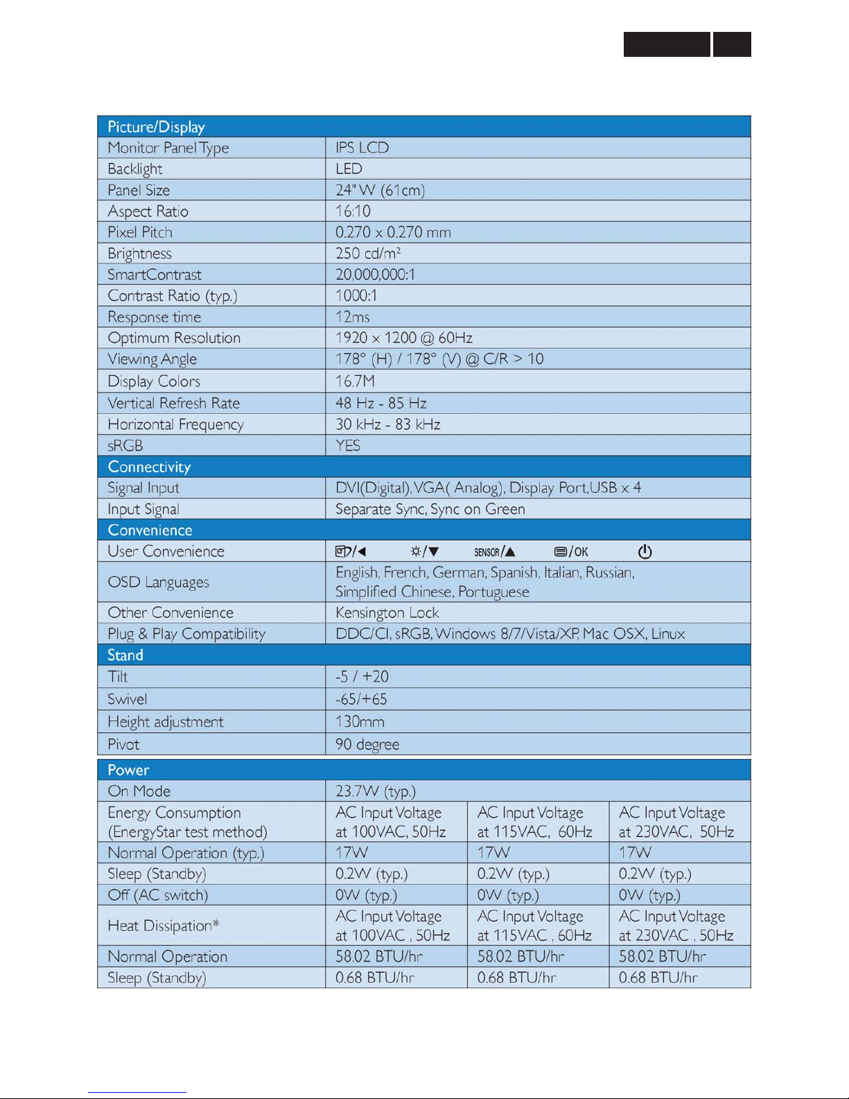
1. Monitor Specifications
Technical specifications
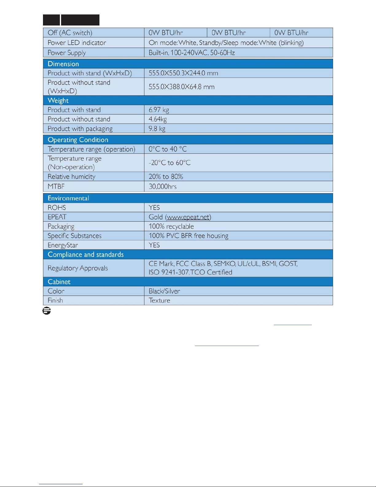
!
!
Meridian 3
6
Note:
1. EPEAT Gold or Silver is valid only where Philips registers the product. Please visit www.epeat.net
for
registration status in your country.
2. This data is subject to change without notice. Go to www.philips.com/support
to download the latest
version of leaflet.
7
Meridian 3
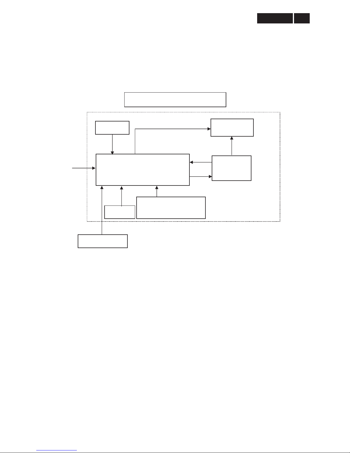
2. LCD Monitor Description
The LCD monitor will contain a scaler board, a power board, an IR board, a head phone jack board (only for
240P4QPYE) and a key board. The scaler board houses the flat panel control logic, brightness control logic and
DDC.
The power board will provide AC to DC inverter voltage to drive the backlight of panel and the scaler board chips
each voltage.
Monitor Block Diagram
LED Panel
Power Board
LED Drive
Key Board
Video signal, DDC
HOST Computer
AC IN
100 ~ 240 V
Scaler Board
(
Include: Audio
)
IR Board
Head Phone Jack Board
(
Only for 240P4QPYE
)
!
!
Meridian 3
8
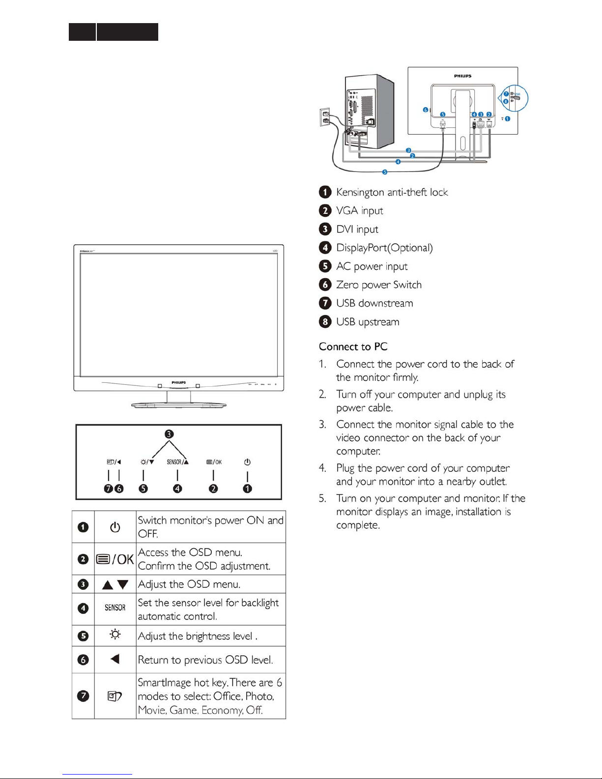
3. Operating Instructions
3.1 General Instructions
Press the power button to turn the monitor on or off.
The other control knobs are located at front panel of
the monitor. By changing these setting, the picture
can be adjusted to your personal preference.
γThe power cord should be connected.
γ Press the power button to turn on the monitor.
The power indicator will light up.
3.2 Control Buttons
Operating the Monitor
Connecting to your PC
9
Meridian 3
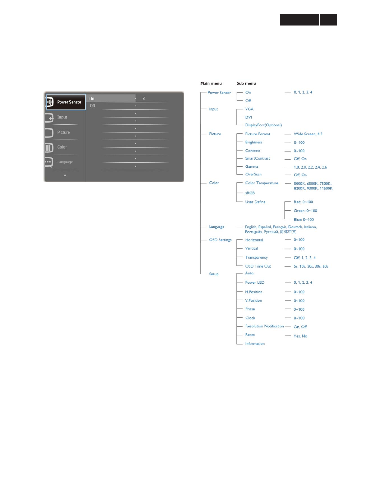
3.3 OSD Menu
On-screen Display (OSD) is feature in all Philips LCD
monitors. It allows an end user to adjust screen
performance or select functions of the monitors directly
through an on-screen instruction windows. A user
friendly on screen display interface is shown as below:
Basic and simple instruction on the control keys
In the OSD shown above, you can pressźŸ buttons
at the front bezel of the monitor to move the cursor,
and press OK button to confirm the choice or change.
The OSD Menu
Below is an overall view of the structure of the
On-Screen Display. You can use this as a reference
when you want to work your way around the different
adjustments later on.
!
!
Meridian 3
10
4. Input/ Output Specification
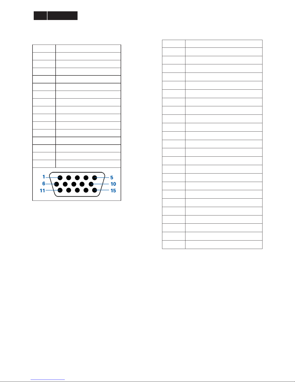
4.1 Input Signal Connector
D-sub Connector
Pin No. Signal Name
1 Red
2 Green/ SOG
3 Blue
4 Sense (GND)
5 Cable Detect (GND)
6 Red GND
7 Green GND
8 Blue GND
9 DDC +3.3V or +5V
10 Logic GND
11 Sense (GND)
12 Bi-directional data
13 H/H+V sync
14 V-sync
15 Data clock
DVI Connector
Pin No. Signal Name
1 T.M.D.S. data22 T.M.D.S. data2+
3 T.M.D.S. data2 shield
4 No Connect
5 No Connect
6 DDC clock
7 DDC data
8 No Connect
9 T.M.D.S. data110 T.M.D.S. data1+
11 T.M.D.S. data1 shield
12 No Connect
13 No Connect
14 +5V Power
15 Ground (for +5V)
16 Hot plug detect
17 T.M.D.S. data018 T.M.D.S. data0+
19 T.M.D.S. data0 shield
20 No Connect
21 No Connect
22 T.M.D.S clock shield
23 T.M.D.S. clock+
24 T.M.D.S. clock-
11
Meridian 3
DP Connector
Pin No. Description
1 ML_Lane 3(n)
2 Ground
3 ML_Lane 3(p)
4 ML_Lane 2(n)
5 Ground
6 ML_Lane 2(p)
7 ML_Lane 1(n)
8 Ground
9 ML_Lane 1(p)
10 ML_Lane 0(n)
11 Ground
12 ML_Lane 0(p)
13 Ground
14 Ground
15 AUX_CH (P)
16 Ground
17 AUX_CH (N)
18 Hot Plug Detect
19 Return DP_PWR
20 DP_PWR
!
!
Meridian 3
12
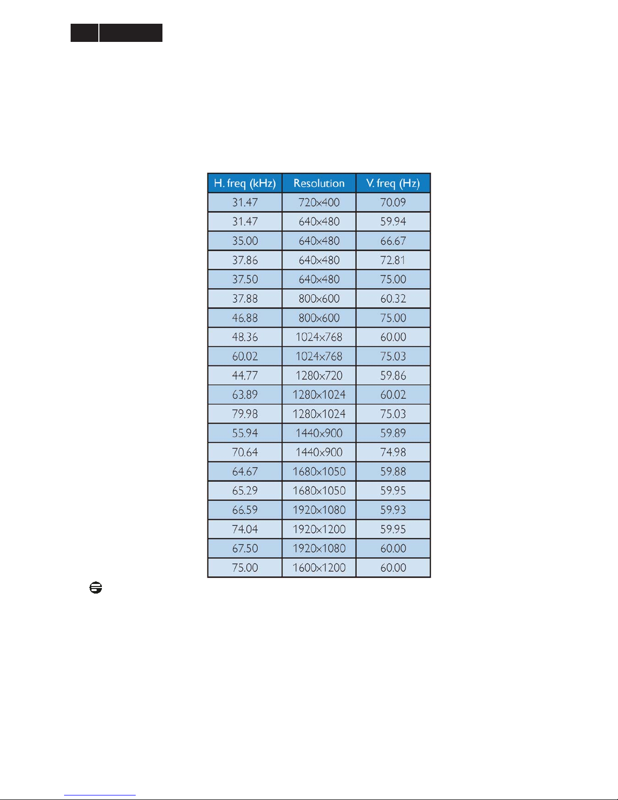
4.2 Resolution & Preset Modes
Maximum Resolution
1920 x 1200 at 60 Hz (analog input)
1920 x 1200 at 60 Hz (digital input)
Recommended Resolution
1920 x 1200 at 60 Hz (digital input)
Note:
Please notice that your display works best at native resolution of 1920 x 1200@60Hz. For be st display qualit y,
please follow this resolution recommendation.
Power Management Definition
If you have VESA DPM compliance display card or software installed in your PC, the monitor can automatically
reduce its power consumption when not in use. If an input from a keyboard, mouse or other input device is
detected, the monitor will 'wake up' automatically. The following table shows the power consumption and signaling
of this automatic power saving feature:
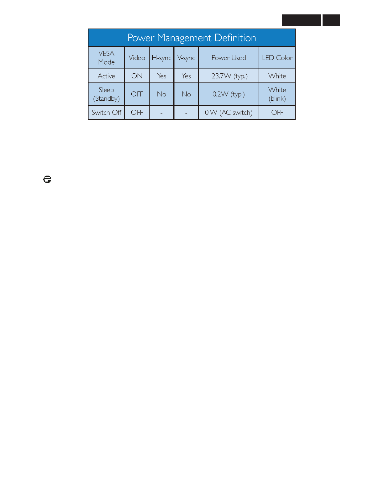
13
Meridian 3
The following setup is used to measure power consumption on this monitor.
·Native resolution:1920×1200
·Contrast: 50%
·Brightness: 250 nits
·Color temperature:6500k with full white pattern
Note:
This data is subject to change without notice.
!
!
Meridian 3
14
4.3 Pixel Defect Policy
Philips strives to deliver the highest quality products.
We use some of the industry’s most advanced
manufacturing process and practice stringent quality
control. However, pixel or sub pixel defects on the TFT
Monitor panels used in flat panel monitors are
sometimes unavoidable. No manufacturer can
guarantee that all panels will be free from pixel defects,
but Philips guarantees that any monitor with an
unacceptable number of defects will be repaired or
replaced under warranty. This notice explains the
different types of pixel defects and defines acceptable
defect levels for each type. In order to qualify for repair
or replacement under warranty, the number of pixel
defects on a TFT Monitor panel must exceed these
acceptable levels. For example, no more than
0.0004% of the sub pixels on a monitor may be
defective. Furthermore, Philips sets even higher quality
standard for certain types or combinations of pixel
defects that are more noticeable than others. This
policy is valid worldwide.
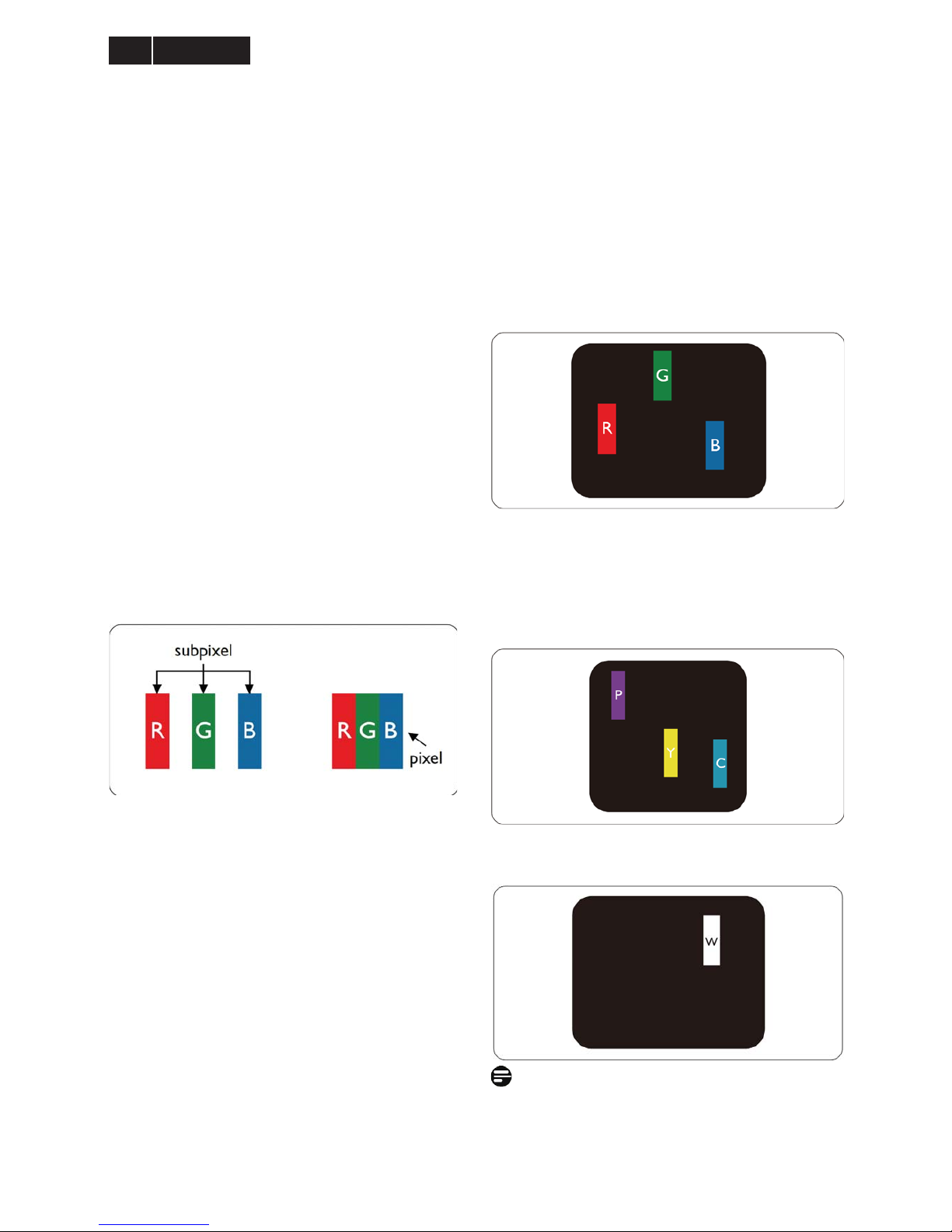
Pixels and Sub pixels
A pixel, or picture element, is composed of three sub
pixels in the primary colors of red, green and blue.
Many pixels together form an image. When all sub
pixels of pixel are lit, the three colored sub pixels
together appear as a single white pixel. When all are
dark, the three colored sub pixels together appear as a
signal black pixel. Other combinations of lit and dark
sub appear as single pixels of other colors.
Types of Pixel Defects
Pixel and sub pixel defects appear on the screen in
different ways. There are two categories of pixel
defects and several types of sub pixel defects within
each category.
Bright Dot Defects Bright dot defects appear as pixel s
or sub pixels that are always lit or ‘on’. That is, a bright
dot is a sub-pixel that stands out on the screen when
the monitor displays a dark pattern. There are three
types of bright dot defects:
One lit red, green or blue sub pixel
Two adjacent lit sub pixels:
- Red + Blue = Purple
- Red + Green = Yellow
- Green + Blue = Cyan (Light Blue)
Three adjacent lit sub pixels (one white pixel)
Note:
A red or blue bright dot must be more than 50 percent
brighter than neighboring dots while a green bright dot
is 30 percent brighter than neighboring dots.
15
Meridian 3
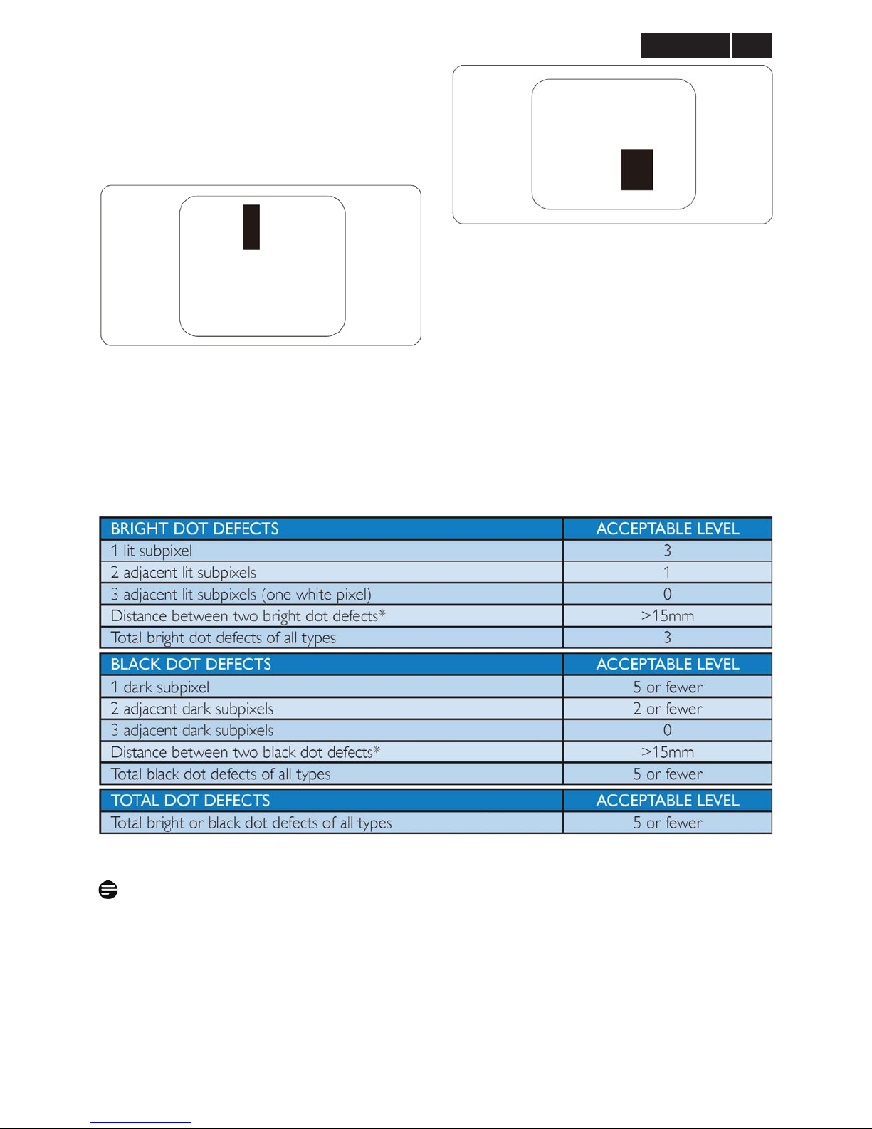
Black Dot Defects Black dot defects appear as pixels
or sub pixels that are always dark or ‘off’. That is, a
dark dot is a sub-pixel that stands out on the screen
when the monitor displays a light pattern. There are
two types of black dot defects:
Proximity of Pixel Defects
Because pixel and sub pixels defects of the same type
that are near to one another may be more noticeable,
Philips also specifies tolerances for the proximity of
pixel defects.
Pixel Defect Tolerances
In order to qualify for repair or replacement due to pixel
defects during the warranty period, a TFT LCD p anel in
a Philips flat panel monitor must have pixel or sub pixel
defects exceeding the tolerances listed in the followin g
tables.
Note:
1. 1 or 2 adjacent sub pixel defects = 1 dot defect.
2. This monitor is ISO9241-307 compliant .Class-I compliant.(ISO9241-307: Ergonomic requirement,analy sis and
compliance test methods for electronic visual displays)
3. ISO9241-307 is the successor of formerly known ISO13406 standard, which is withdrawn by the International
Organisation for Standardisation (ISO) per: 2008-11-13.
!
!
Meridian 3
16
4.4 Failure Mode Of Panel
Failure description
Phenomenon
Vertical block defect
Vertical dim lines
Vertical lines defect
(Always bri
g
ht or dark)
Horizontal block defect
Horizontal dim lines
Horizontal lines defect
(Always bri
g
ht or dark)
Has bri
g
ht or dark pixel
Polarizer has bubbles
Polarizer has bubbles
Foreign material inside
polarizer. It shows liner or
dot shape.
Concentric circle formed
Bottom back light of LCD is
brighter than normal
Back light un-uniformity
Backli
g
ht has foreign material.
Black or white color, liner or
circular type
Quick reference for failure mode of LCD panel
this pa
g
e presents problems that could be made by LCD panel.
It is not necessary to repair circuit board. Simply follow the mechanical
instruction on this manual to eliminate failure by replace LCD panel.
17
Meridian 3
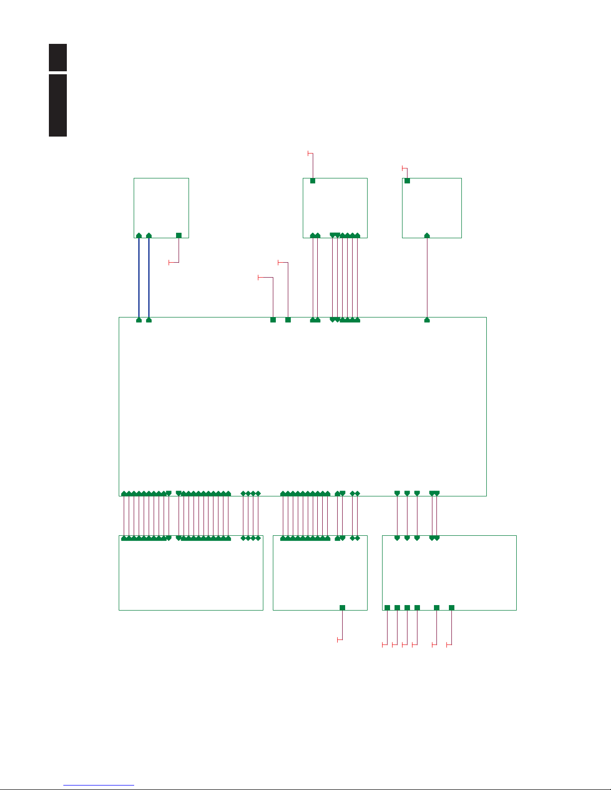
5. Block Diagram
5.1 Scaler Board
PA[0..9]
PB[0..9]
+16V
V33S-DP
+16V
V33S-DP
AUDIO
7. Audio
V5A
Volume
Mute
AIN_R
AIN_L
AOUT_R
AOUT_L
AUDIO_5V
Audio_SD
V5A
USB
8.USB
+16V
DC POWER SAVING
DISPLAY PORT
3.DI SPLAY PORT
DP_SINK_ASS_1
DP_SINK_ASS_2
LANE2P
LANE2N
LANE0P
LANE0N
DET_DP
LANE3N
LANE3P
LANE1N
LANE1P
V33S-DP
AUX_CHP
AUX_CHN
DP_HOT_PLUG
INPUT
2.INPUT
RIN
GIN
BIN
VSYNC
GNDR
GNDG
GNDB
HSYNC
SOG
RX0-
RX1+
RX1-
RX2-
RXC-
RX2+
RXC+
RX0+
DVI_SDA
DVI_SCL
DDC_WP
DVI_HPD
DET_DVII
DDCA_SCL
DDCA_SDA
DET_VGAI
SCALER
4.SCALER
V33S
V12S
PB[0..9]
HSYNC
GIN
SOG
VSYNC
GNDG
BIN
GNDR
RIN
GNDB
RX0-
RX2+
RX0+
RX2-
RXC-
RXC+
RX1+
RX1-
on_PANEL
PA[0..9]
on_BACKLIGHT
adj_BACKLIGHT
DET_DP
DVI_HPD
DDC_WP
DET_DVII
DVI_SCL
DVI_SDA
LANE3N
LANE3P
LANE2N
LANE2P
LANE1N
LANE1P
LANE0N
LANE0P
DP_SINK_ASS_1
DP_SINK_ASS_2
AUX_CHP
AUX_CHN
DP_HOT_PLUG
DDCA_SCL
DDCA_SDA
DET_VGAI
Volume
Mute
AIN_R
AIN_L
AOUT_R
AOUT_L
AUDIO_5V
PS_ON
Audio_SD
PANEL12V_ON
DC POWER SAVING
PANEL I N TERF ACE
5.PANEL I N TERF ACE
PB[0..9]
PA[0..9]
VLCD
POWER
6.POW ER
on_PANEL
VLCD
V12S
V33S
V5A
on_BACKLIGHT
adj_BACKLIGHT+16V
V33S-DP
PS_ON
PANEL12V_ON
V12S
V33S
V12S
VLCD
VLCD
V33S
V5A
!
!
Meridian 3
18
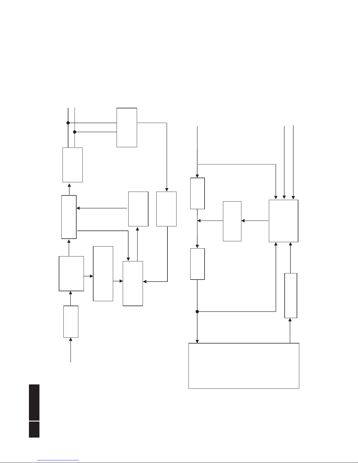
5.2 Power Board
DIM
ON/OFF
Feedback Circuit
MOSFET
(Q801)
PWM Control
OZ9997GN
(IC801)
16V
LED
(CN802)
ZD802 L801
16V
EMI filter
Start Re sistor
(R905,R908)
PWM Control
(IC901)
Transformer
AC input
Bridge
Rectifier
and Filter
Feedback
Circuit
Rectifier
diodes
Power Switch
(Q901)
Photo coupler
(IC902)
5V
19
Meridian 3
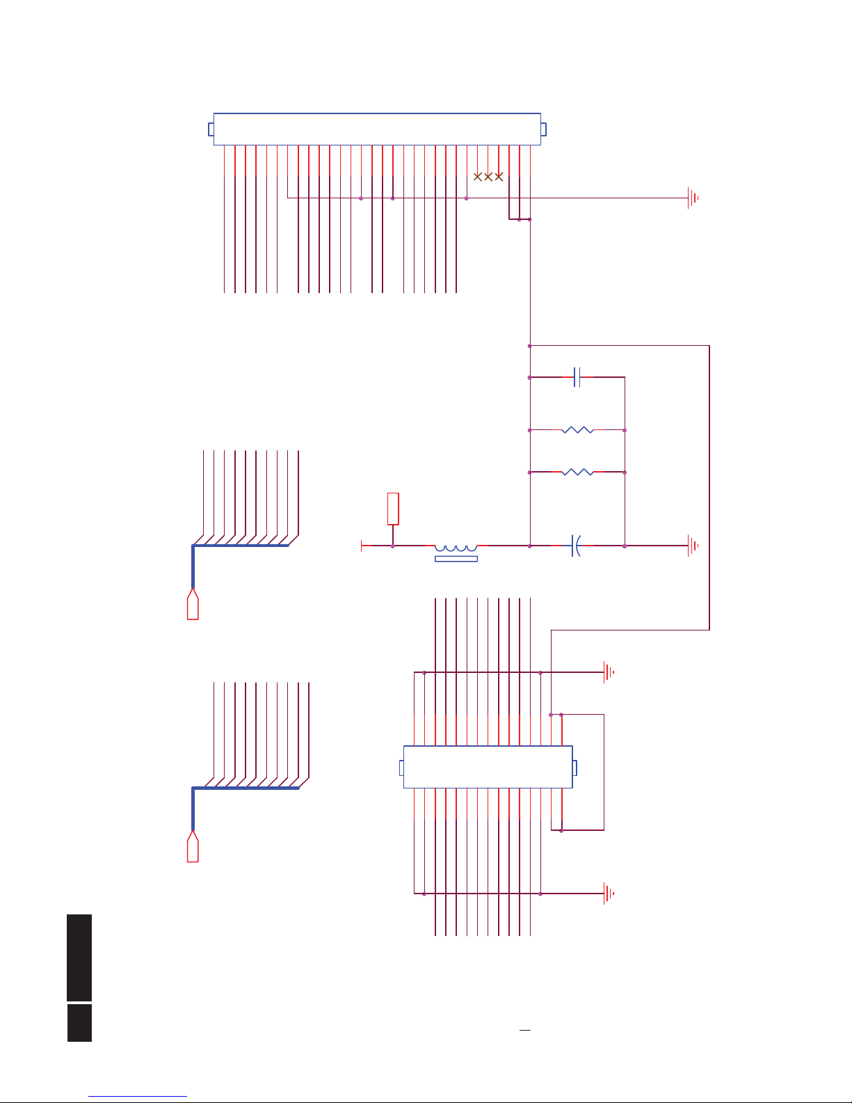
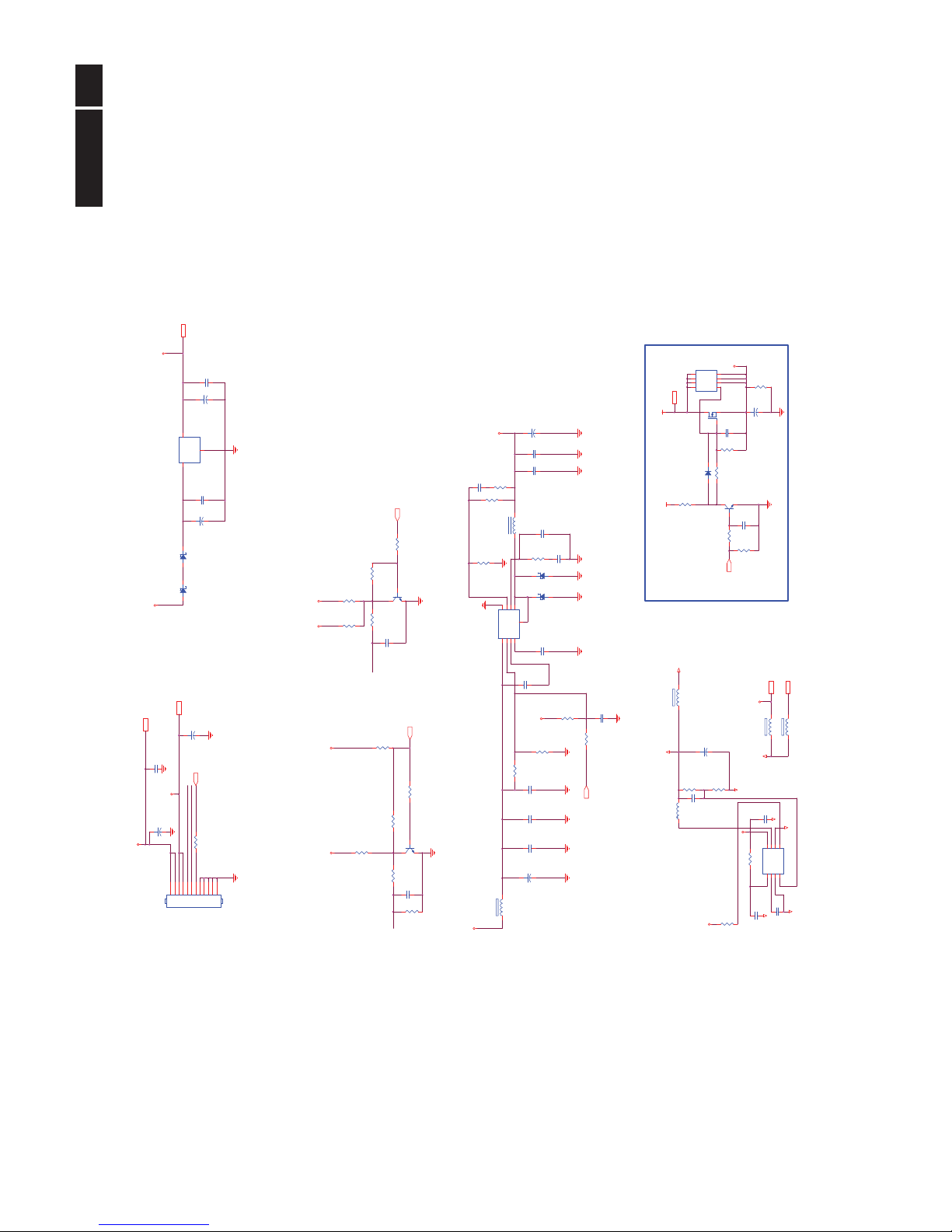
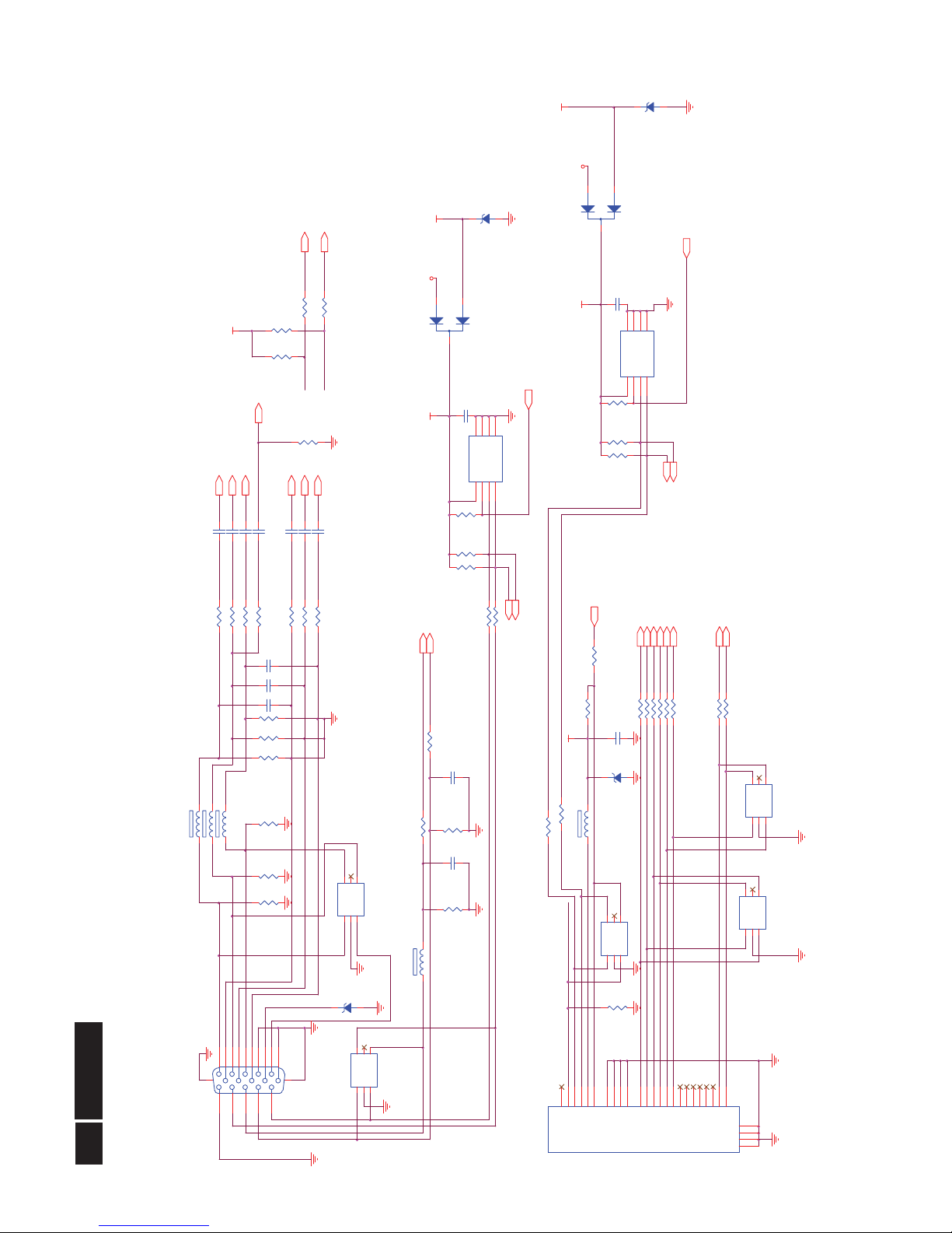
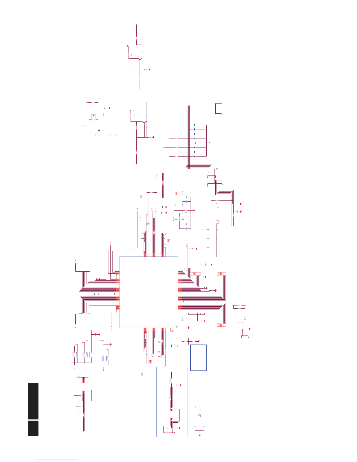
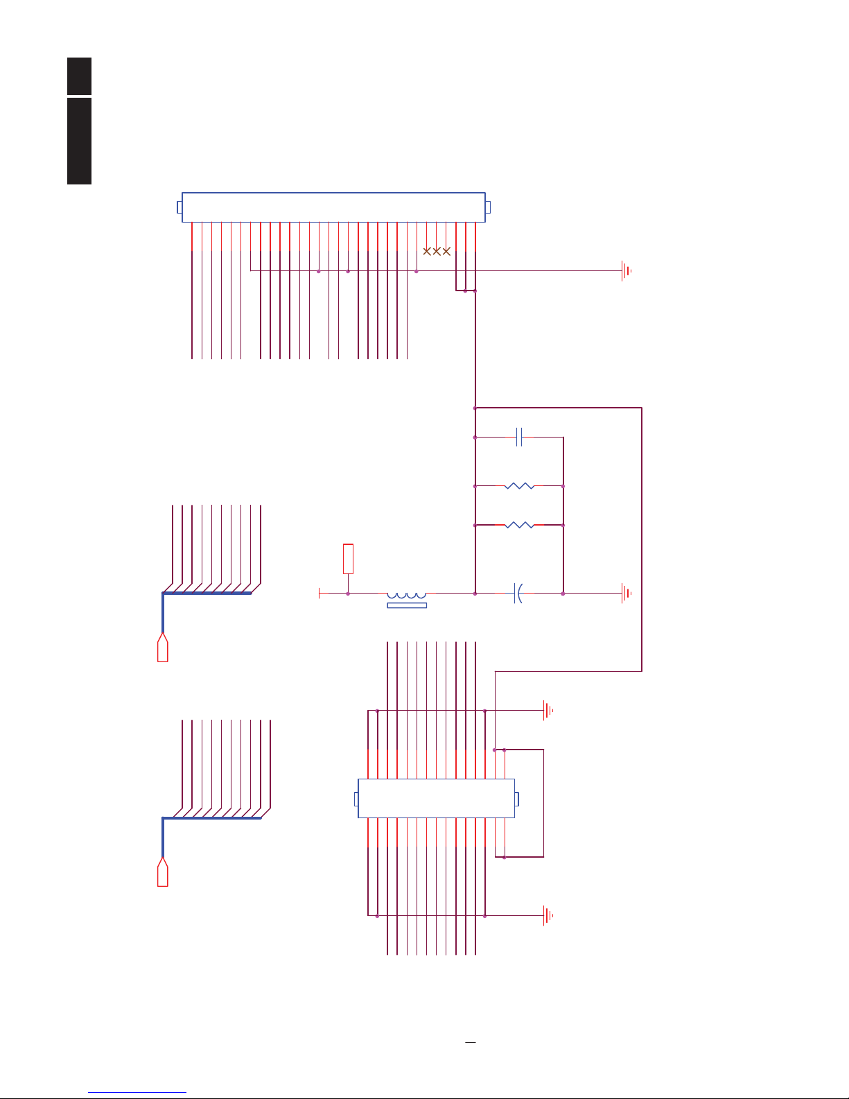
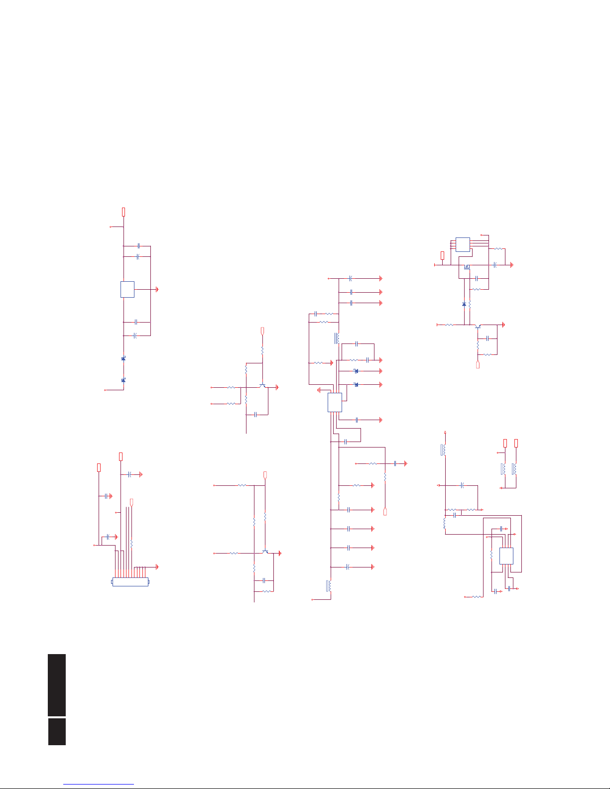
6. Schematic
6.1 Scaler Board (715G5774M01000004K)
Remark: Parts position can be searched by using FIND function in PDF.
ESD_5V
R105 1K C105 22N 25V
V5A
V5A
D102
BAT54C
3
1
2
DAT1-
DDC_WP
DVI5V
DAT1+
DAT0-
SCL_VGA
C102 47N16VR102 100OHM
R133 10 OHM
R135 10 OHM
RED-
R138 10 OHM
GREEN-
BLUE-
R111 100OHM
R137 10 OHM
R10675R 1/16W 1%
R110 100OHM
R141 10 OHM
ZD102
RLZ5.6B
1 2
HPD
R140 10 OHM
R136 10 OHM
R114 100OHM
DET_VGA
SCL_DVI
R134 10 OHM
DET_DVI
RIN 5
GNDR 5
VSYNC 5
BIN 5
GIN 5
R112
NC/1M 1/ 16W 5%
R139 120R 0.3A
12
DET_VGAI 5
HSYNC 5
GNDB 5
GNDG 5
R115 100OHM
SOG 5
RX1- 5
RX0- 5
RX1+ 5
DVI_SDA5
DDCA_SCL5
DDCA_SDA5
RX2+ 5
RX0+ 5
RXC- 5
RXC+ 5
DVI5V
VGA5V
RED+
DVI_SCL5
DDC_WP 5
DDC_WP 5
HSI
U101
CAT24C02WI-GT3A
A01A12A2
3
GND
4
SDA5SCL6WP7VCC
8
U103
CAT24C02WI-GT3A
A01A12A2
3
GND
4
SDA5SCL6WP7VCC
8
DET_DVI
C118
220N 10V
R122
4.7K1/16W
C116
220N 10V
RX2- 5
DAT0+
GREEN+
R121 4.7K1/16W
R120 4.7K1/16W
R124 47R 1/16W 5%
R130 4.7K1/16W
R123 47R 1/16W 5%
R131 4.7K1/16W
DDC_WP
U109
AZC398-04S
I/O11GND2I/O2
3
I/O3
4
NC
5
I/O4
6
R119
22K1/16W
R118
22K1/16W
R116 470OHM1/16W
C1075PF 50V
C1085PF 50V
DAT2-
DAT2+
C1065PF 50V
R113 100OHM
ZD101
RLZ5.6B
1 2
R109
NC/ 22K 1/ 16W 5%
R108
NC/22K 1/16W 5%
VSI
DCLK+
DCLK-
FB101 19R 0.5A
1 2
FB103 19R 0.5A
1 2
FB102 19R 0.5A
1 2
FB104 120R
R127 1K
CN101
DB15
162738495
1112131415
10
1716
DET_DVII 5
R129
NC
R125 47R 1/16W 5%
DET_VGA
SDA_DVI
ESD_VGA
VGA5V
D101
BAT54C
3
1
2
CN102
JACK
DAT2-
1
DAT2+
2
2/4shield
3
DAT4-
4
DAT4+
5
DDC SCL
6
DDC SDA
7
VSYNC
8
DAT1-
9
DAT1+
10
1/3shield
11
DAT3-
12
DAT3+
13
+5V
14
SYNC GN D
15
HPD
16
DAT0-
17
DAT0+
18
0/5shield
19
DAT5-
20
DAT5+
21
clk shield
22
clk+
23
clk-
24
GND
26
GND
25
GND
27
GND
28
U110
AZC398-04S
I/O11GND2I/O2
3
I/O3
4
NC
5
I/O4
6
U102
AZC398-04S
I/O11GND2I/O2
3
I/O3
4
NC
5
I/O4
6
U104
AZC398-04S
I/O11GND2I/O2
3
I/O3
4
NC
5
I/O4
6
U105
AZC398-04S
I/O11GND2I/O2
3
I/O3
4
NC
5
I/O4
6
ZD103
NC/RLZ5.6B
ZD104
NC/RLZ5.6B
C115
22P 50V
ESD_DVI
C117
100N 16V
SDA_VGA
R128
NC/ 4K7 1/ 16W 5%
DVI_HPD 5
R101
75R 1/16W 1%
R10775R 1/16W 1%
R103 100OHM
R104 100OHM
R163
NC/75R 1/16W 1%
R162
NC/75R 1/16W 1%
R164
NC/75R 1/16W 1%
C114
22P 50V
BLUE+
R126 47R 1/16W 5%
R132
4.7K1/16W
C103 47N16V
C104 47N16V
C109 47N16V
C110 47N16V
C111 47N16V
ESD_5V
ESD_5V
R117 470R 1/16W 5%
INPUT
!
20
Meridian 3
Remark: Parts position can be searched by using FIND function in PDF.
R159
1K
DP_SINK_ASS_2 5
DP_SINK_ASS_1 5
U108
AZC398-04S
I/O11GND2I/O2
3
I/O3
4
NC
5
I/O4
6
R165
100K1/16W
R161
NC/ 10K 1/16W 5%
R167 0R05 1/16W
R168 0R05 1/16W
DP_VDD
need to layer
Differential Trace
CN103
DP CONN
SHELL1
21
SHELL2
22
ML_ Lane 3(n)
1
GND
2
ML_ Lane 3(p)3ML_ Lane 2(n)
4
GND
5
ML_ Lane 2(p)6ML_ Lane 1(n)
7
GND
8
ML_ Lane 1(p)9ML_ Lane 0(n)
10
GND
11
ML_ Lane 0(p)
12
GND13GND
14
AUX_CH(p)
15
GND
16
AUX_CH(n)
17
Hot Plug Detect
18
Return
19
SHELL4
24
SHELL3
23
DP_PWR
20
R156 0R 05 OHM
DP_VDD
AUX_CHP 5
AUX_CHN 5
DP_HOT_PLUG 5
AUX_CHP
DP_VDD
ZD105
NC/RLZ5.6B
1 2
DP_VDD
LANE3P
LANE3N
LANE2P
LANE2N
LANE1P
LANE1N
LANE0N
LANE0P
R151
1M 1/16W
R152
NC
AUX_CHN
R154 0R 05 OH M
t
F101
PTCR
1 2
V33S-DP7
U107
AOZ8804DI
CH11CH22VN3CH34CH4
5
NC6NC
7
VN
8
NC9NC
10
LANE0P
LANE0N
LANE1P
LANE1N
LANE2N
LANE2PLANE2P
LANE3P
LANE3N
DP_VDD
R166
NC/ 0R 05 1/ 16W
U106
AOZ8804DI
CH11CH22VN3CH34CH4
5
NC6NC
7
VN
8
NC9NC
10
C122
100N 16V
R153 1K
R157
NC
R158
1M 1/16W
DET_DP 5
R150 100OHM
LANE2N
LANE2P
LANE0P
LANE3N
LANE0N
LANE3P
LANE1P
LANE1N
LANE0P 5
LANE0N 5
LANE3P 5
LANE3N 5
LANE1P
LANE0N
LANE1N
LANE0P
LANE2N 5
LANE1N 5
LANE2P 5
LANE1P 5
LANE3P
LANE2P
LANE3N
LANE2N
C120
100N 16V
DISPLAY PORT

21
Meridian 3
Remark: Parts position can be searched by using FIND function in PDF.
R436 NC/ 0R 05 OHM
CN402,CN403 BOTH LAYOUT
Pin 118
PW ON Latch:
Internal MCU :Pull High
External MCU :Pull Low
POWER
V12C
V33SDRAM
R482 100OHM
WP_PRO
DDC_WP 3
R439
NC/22K 1/16W 5%
C404
100N 16V
R418
4.7K1/16W
on_BACKLIGHT7
+
C423
NC/10UF50V
+
C418
100UF 16V
PS_ON7
PWM4
CN401
CONN
12345
DVI_HPD3
AOUT_R1
V33TMDS
Adj_BACKLIGHT7
CN402
CONN
1234567891011
12
PANEL12V_ON7
DP_HOT_PLUG4
X401
14.31818MHZ/32PF
12
R422 NC
R423 NC
C420 1uF 10V
KEY2
LED_1
AUDIO_5V8
LED_2
V33TMDS
CN403
NC/CONN
12345
6
R430 100OHM
V33SDRAM
AOUT_L1
R431 100OHM
V33LSADC
R425
10K
V33CRYSTAL
KEY1
KEY2
FB407 120R
PA0
PA1
V12ADC
PA2
R416 560R 1/16W 5%
Mute 8
Mute
PA3
+
C403
100UF 16V
R435
NC/0R05 OHM
PA4
R437
NC/0R05 OHM
C427
NC/1N 50V
FB401 120R
DVI_SDA3
DVI_SCL3
PA6
PA5
PA7
R407 0R05 OHM
R408 0R05 OHM
R417
NC/1M 1/16W 5%
PS_DISTANCE
FB406 120R
DET_DP 4
PA8
PA9
DET_DP
PB0
PB1
PB2
R411
NC
R412
10K
C409
220N 10V
PB3
VCC3.3
WP
SDOUTCESDIN
R41422R 1/16W 5%
R41522R 1/16W 5%
R41322R 1/16W 5%
R440
47K 1/16W 5%
PB4
PB5
GNDG 3
SOG 3
GNDR 3
RIN 3
HSYNC 3
GIN 3
GNDB 3
BIN 3
VSYNC 3
+
C417
100UF 16V
Audio_SD 8
XO
PB6
PB7
PB9
PB8
R404
4K7 1/16W 5%
R424
10K
LED driver
C401
220N 10V
R402 4.7K1/16W
C428
NC/1N 50V
R403 4.7K1/16W
PA[0..9] 6
V33P
TO Processor Board
PB[0..9]6
CLK
R455
100K1/16W
RX2+ 3
RX1+ 3
RX2- 3
RX0- 3
C429
100N 16V
C440
10UF 10V
RX1- 3
RXC- 3
RX0+ 3
RXC+ 3
Q403
LMBT3904LT1G
R454
4.7K1/16W
C441
100N 16V
OC_SW
Q404
LMBT3904LT1G
VCC3.3
VCC3.3
OC401
ISA401
Cathode
1
Anode
2
Emitter2
3
Collector
4
Emitter1
5
R457 10K
R456 NC/10K
R453
620 OHM 1/16W
VCC3.3
C435100N 16V
R458
22K1/16W
R459
10K
Q402
LMBT3906LT1G
R445
NC/10K
WP_PRO
C442
100N 16V
R474
NC
C434100N 16V
ZD401
RLZ5.6B
1 2
LED_A
R444 NC/100OHM
LED_A
R463
NC
R447NC
LED_1
R473
56 OHM +-5% 1/8W
LED_2
R490
0R05 OHM
R443 NC/100OHM
R472
0R05 OHM
V5A
C410
NC/10pF 16V
V5A
LANE1P4
LANE3P4
C421
100N 16V
R406
0R05 OHM
LANE0P4
LANE2N4
LANE0N4
LANE2P4
LANE1N4
WP
LANE3N4
DET_DVII
DET_VGAI
For Auto Pivot Function
DET_DP
ZD402
RLZ5.6B
1 2
R467
10K
R448NC
C433NC
C407 100N 16V
AUX_CHP4
C430
NC
EESCLEE_SCL
R4503.9K1/16W
R465
NC
R410 1K
C432NC
EESDAEE_SDA
R464
NC
C431NC
Q401
LMBT3906LT1G
R470
NC
R471
NC
R462 0R05 OHM
R460
10K
R4513.9K1/ 16W
R446
NC/10K
R426 0R 05 OH M
DDCA_SDA 3
R469
22K1/16W
R427 0R 05 OH M
DDCA_SCL 3
ZD403
RLZ5.6B
1 2
R4523.9K1/16W
R466
1 OHM +-5% 1/8W
R475
0R05OHM1/8W
R461
22K1/16W
R449NC
R468
NC
PWM1
PWM2
C419100N 16V
C438100N 16V
R486 NC/0R05 OHM
VCC3.3
VCC3.3
VCC3.3
VCC3.3
AOUT_L1
C406 100N 16V
AUX_CHN4
AOUT_R1
AIN_R 8
AIN_L 8
AOUT_L 8
AOUT_R 8
R420
6.2KOHM 5% 1/16W
R405
100OHM
DP_SINK_ASS_2 4
ERGO_ON
FB408
120R
12
R401
100OHM
UART_TXD
UART_RXD
P53
ERGO_ON
PS_OUTPUT
PS_DISTANCE
R421
NC
P52
LED_G
LED_A
+
C422
100UF 16V
C416
100N 16V
DDCA_SCL 3
DDCA_SDA 3
C425
100N 16V
R433 NC
R434 NC
+
C408
NC/10UF16V
U403
M24C16
A01A12A2
3
GND
4
SDA5SCL6WP7VCC
8
U402
MX25L4006EM1I-12G
CE#
1
SO
2
WP#
3
GND
4
VDD8HOLD#7SCK6SI
5
VCC3.3
R409
4.7K1/16W
P53
+
C424
NC/10UF50V
P52
C439
NC/1N 50V
C426
NC/1N 50V
EESCL
EESDA
Near to scalar
DET_VGAI
R441
47K 1/16W 5%
DET_VGAI 3
DET_DVII 3
DET_DVII
R442
47K 1/16W 5%
VCC3.3
VCC3.3
VCC3.3
on_Panel 7
POWER
on_Panel
LED_G
C414
100N 16V
V5A
V5A
V5A
R432
NC/10K 1/16W 5%
U401
RTD2486T D-GR
DP_VDD/TMDS_VDD
1
TMDS_REXT
2
LANE0P/RX2P_0
3
LANE0N/RX2N_0
4
LANE1P/RX1P_0
5
LANE1N/RX1N_0
6
LANE2P/RX0P_0
7
LANE2N/RX0N_0
8
LANE3P/RXCP_0
9
LANE3N/RXCN_0
10
DP_GND/TMDS_GND
11
LANE0P/RX2P_1
12
LANE0N/RX2N_1
13
LANE1P/RX1P_1
14
LANE1N/RX1N_1
15
LANE2P/RX0P_1
16
LANE2N/RX0N_1
17
LANE3P/RXCP_1
18
LANE3N/RXCN_1
19
DP_VDD/TMDS_VDD2
20
AVS0
21
AHS0
22
ADC_VDD
23
B0-
24
B0+
25
G0-
26
G0+
27
SOG0
28
R0-
29
R0+
30
GPI/GPO/V8_7
31
GPI/GPO / V8_6
32
ADC_GND
38
GPI/GPO/V8_1
37
GPI/GPO/V8_2
36
GPI/GPO / V8_3
35
GPI/GPO / V8_4
34
GPI/GPO/ V8_5
33
AUDIO_SOUTL/ V8_3/SCK/G PIO
45
SPDIF3/AUDIO_REF/V8_4/WS/GPIO
44
A-ADC0/VCLK/GPIO
50
A-ADC1/GPI O51A-ADC2/GPI O52A-ADC3/GPI O53A-ADC4/GPI O
54
TCON[0][5]/BADC0/PWM1/PWM5/GPIO
55
TCON[1][4]/B-ADC1/IICSCL/GPIO
56
V8_7/GPIO
41
TCON[9][11]/B-ADC2/IICSDA/GPIO
57
TCON[7][10]/DDCSCL1/GPIO
58
TCON[3][5]/DDCSDA1/GPIO
59
VCCK
60
PGND
61
PVCC
62
TCON[1][8]/PWM2/GPIO
63
SD0/SPDIF0/TCON[0][7]/GPIO/IrDA
64
AUDIO_HOUTL/V8_1/SD0/GPIO
47
AUDIO_HOUTR/V8 _0/PWM0/GPIO
48
ABLU7/SCK/TCON[4][2]/GPIO/BB3N
66
ABLU6/MCK/TCON[5][9]/GPIO/BB2P
67
ABLU5/SD0/SPDIF0/TCON[13][3]/GPIO/BB2N
68
LINE_INL/V8_6/IICSCL/GPIO
42
ABLU4/SPDIF1/SD1/TCON[ 7][3]/GPIO/IICSCL/BB1P
69
ABLU3/SPDIF2/SD2/TCON[ 9][11]/GPIO/IICSDA/BB1N
70
ABLU2/SPDIF3/SD3/TCON[10][8]/GPIO/PWM1/PWM5/BCLKP
71
TCON[6][12]/GPIO/PWM3/BCLKN
72
VCCK
73
ABLU1/ GPIO/ABLU7/ T XO3+_8b/TXO4+_10b/BG3P
74
ABLU0/ GPIO/ABLU6/TXO3-_8b/TXO4-_10b/BG3N
75
AGRN7/GPI O/ABLU5/T XOC+_8b/TXO3 +_10b/BG2P
76
AGRN6/GPIO/ABLU 4/TXOC-_8b/TXO3-_ 10b/BG2N
77
AUDIO_SOUTR/V8_2/MCK/GPIO
46
PVCC
84
PGND
85
ARED7/AGRN3/TXE3+_8b/TXO0+_10b/BR1P
86
LINE_INR/V8_5/ IICSDA/GPI O
43
GPIO/PWM3/TCON[11][6]/TXE0-_10b/AG2N
99
GPIOVCLK
40
LS_ADC_VDD
49
MCK/TCON[7]/GPIO/AR1P
108
GPIO/V8_0/
39
XO
127XI128
WS/TCON[7][1]/GPIO/PWM1/BB3P
65
AGRN5/GPIO/ABLU 3/TXO2+_8b/TXOC+_10b/ BG1P
78
AGRN4/GPIO/ABLU2/TXO2-_8b/TXOC-_10b/BG1N
79
AGRN3/GPI O/AGRN7/ TXO1+_8b/TXO 2+_10b/BR3P
80
AGRN2/GPIO/AGR N6/TXO1-_8b/TXO2-_ 10b/BR3N
81
AGRN1/GPI O/AGRN5/ TXO0+_8b/TXO 1+_10b/BR2P
82
AGRN0/GPIO/AGR N4/TXO0-_8b/TXO1-_ 10b/BR2N
83
ARED6/AGRN2/ TXE3-_8b/TXO0-_10b/BR 1N
87
ARED5/ARE D7/TXEC+_8 b/TXE4+_10b/A B3P
88
ARED4/ARED6/TXEC-_8b/TXE4+_10b/AB3N
89
ARED3/ARED5/ TXE2+_8b/TXE3+_10b/AB2P
90
ARED2/ARED4/ TXE2-_8b/TXE3-_10b/AB2N
91
ARED1/ARED3/ TXE1+_8b/TXEC+_10b/AB1P
92
ARED0/ARED2/ TXE1-_8b/TXEC-_10b/ AB1N
93
DENA/TXE0+_8b/T XE2+_10b/ACLKP
94
DHS/TXE0-_8b/T XE2-_10b/ACLKN
95
DCLK/GPIO/PW M0/TXE1+_10b/AG3P
96
DVS/GPIO/PWM 1/TXE1-_10b/AG3N
97
GPIO/PWM2/TX E0+_10b/AG2P
98
GPIO/PWM4/TCON[12][3]/AG1P
100
GPIO/PWM5/TCON[0]/AG1N
101
SD3/ SPDIF3/TCON[10]/GPIO/PWM0/AR3P
102
SD2/SPDIF2/TCON[8]/GPIO/IICSCL/PWM1/AR3N
103
SD1/SPDIF1/TCON[5]/GPIO/I RQ/IICSDA/AR2P
104
SD0 / SPDIF0 / TCON[9] / GPIO / AR2N
105
PVCC
106
PGND
107
SCK/TCON[3]/GPIO/AR1N
109
WS/TCON[6]/GPIO/SDT
110
SD0/SPDIF0/TCON[4]/GPIO/SPDIF1
111
SD1/ SPDIF1/TCON[9]/GPIO/WS
112
SD2/SPDIF2/TCON[1][11]/GPIO/IrDA/SCK
113
SD3/SPDIF3/TCON[13]/GPIO/VC LK/ MCK
114
SPI_SCLK/SeriesData
115
SI/MCU_SCLK
116
SO/SCSB
117
CEB/IRQB
118
GPIO/PWM5/SPDIF1
119
VCCK
120
DDCSCL3/GPIO/AUX-CH_P1
121
DDCSDA3/ GPIO/AUX-CH _N1
122
DDCSCL2/GPIO/AUX-CH_P0
124
DDCSDA2/ GPIO/AUX-CH _N0
123
RESETB
125
CEC/GPIO/PWM1/SPDIF2
126
E-Pad
129
V33SDRAM
OC_SW
SDOUT
CLKCESDIN
on_Panel
CE
V33CRYSTAL
DP_SINK_ASS_1 4
V33TMDS
V12C
R428 NC
R429 NC
DC POWER SAVING9
XI
Volume
V33P
XO
Volume 8
PS_OUTPUT
UART_TXD
UART_RXD
C405
100N 16V
KEY1
KEY2
R438
NC/22K 1/16W 5%
C411
22P 50V
V12S7
V12CV12S
V33S7
VCC3.3 V33P
R419
NC/4K7 1/16W 5%
V12ADC
C412
22P 50V
V12C
V33LSADC
KEY1
ERGO_ON
FB402 120R
V33P
FB405 120R
FB403 120R
V33P
FB404 120R
XI
Scaler
!
22
Meridian 3
Remark: Parts position can be searched by using FIND function in PDF.
C437
100N 16V
C429,C431 lay
ǂ
LVB1PPB6
LVB2MPB5
LVB1MPB7
LVB3MPB1
LVB3PPB0
LVBCKPPB2
LVBCKMPB3
LVB2PPB4
PB[0..9]
FB409
120R 6A
1 2
R4811.5K 1/4W
CN408
CONN
246810
12
14
16
18
20
22
24
26
28
30
13579
11
13
15
17
19
21
23
25
27
29
CN407
NC/CONN
123456789
10
11
12
13
14
15
16
17
18
19
20
21
22
23
24
25
26
27
28
29
30
LVB0PPB8
LVB0MPB9
RXO0- RXO0+
RXO1- RXO1+
R4801.5K 1/4W
RXO2-
PA6 LVA1P
PA5 LVA2M
RXO2+
PA0 LVA3P
PA4 LVA2P
PA3 LVACKM
PA1 LVA3M
PA7 LVA1M
PA[0..9]
RXOC-
PA8 LVA0P
RXOC+
RXO3- RXO3+
RXE0-
PB[0..9]5PA[0..9]5
RXE0+
VLCD 7
VLCD
RXE1- RXE1+
RXE2- RXE2+
RXEC- RXEC+
option
RXE3- RXE3+
PA9 LVA0M
LVA0P RXE0+
PA2 LVACKP
RXE3-LVA3M
RXO3-LVB3M
RXE2-LVA2M
RXE1-LVA1M
LVB2M RXO2-
RXO1-LVB1M
RXO0-LVB0M
LVACKM RXEC-
LVBCKM RXOC-
RXE0-LVA0M
RXOC+LVBCKP
RXO0+LVB0P
RXE2+LVA2P
RXO1+LVB1P
RXEC+LVACKP
RXO3+LVB3P
RXO2+LVB2P
RXE1+LVA1P
RXE3+LVA3P
+
C436
150UF 25V
Panel Interface
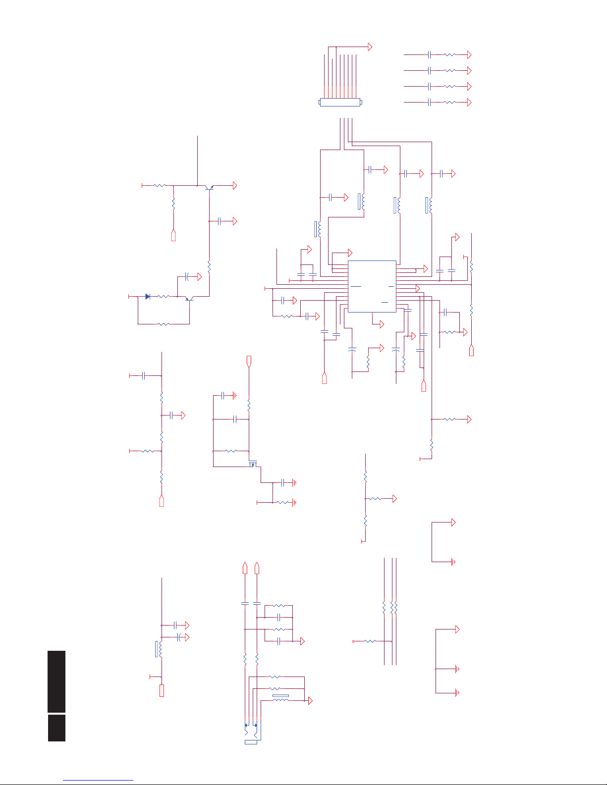
23
Meridian 3
Remark: Parts position can be searched by using FIND function in PDF.
Scaler Core
on_BACKLIGHT 5
Adj_BACKLIGHT 5
PANEL12V_ON5
R702
10K 1/10W 5%
V33S
V5A
V5A R731
10K
BKLT_EN
C726
10N 50V
FB702
120R 6A
L702
2.2uH
FB704
120R 6A
R721
10K 1/10W 5%
R724
4K7 1/10W 5%
FB703
120R 6A
R717
10K 1/16W
R715
4.7K1/16W
+16V
C720
10UF 25V
C724
100NF 25V
V5A
C714
100NF 25V
D703
SX36
1 2
R720
0R05 OHM
C715
1uF 25V
R722
10 OHM
C719
22P 50V
+
C727
220UF 16V
R723
14.7KOHM 1/10W
+
C730
150UF 25V
R728 24K 1/16W 5%
U703
AT1528P11U
VCC1REF2GND3FB
4
EN
5
PGND
6
LX
7
VIN
8
R726
10K
C713
100NF 25V
R714
30Kohm 1/16W +/-5%
Q705
NC/AO3401
C718
22P 50V
Q704
LMBT3904LT1G
C723
100NF 25V
C716
1uF 25V
C728
100N 16V
C729
0.47uF 16V
C725
10UF 10V
C712
10UF 25V
D705
NC/LL4148
+
C722
150UF 25V
R727
10K
VLCD
VLCD 6
on_Panel5
R716
10K
H: OnL:Off
C721
10UF 25V
TCON POWER
+3.3V_SW
+3.3V
GND
GND
GND
C711
10UF 25V
Q706
AO4411
S
1
S
2
S
3
G
4
D
8
D
7
D
6
D
5
+3.3V_SW
+
C710
150UF 25V
R729
NC/47K 1/16W 5%
FB701
48R 6A
1 2
C717
820pF 50V
R730
10K
D704
SX36
1 2
R713 N C/100K1/16W
U702
APW7089KAI-TRG
VIN1EN2UGND3VCC
4
LX
5
COMP
6
FB
7
GND
8
LX
9
GND
GND
R719
62K1/16W
+12V_Panel
+12V_Panel
+12V_Panel
L701
10uH 20%
BKLT_ADJ
R718
140K 1%
AT1528P11U: Max:2A
Vout = 0.8V (1+(ĴR1/R2 ))
Cancel U705
V33S
V33S 5
V33S-DP 4
+16V
R701
100R 1/10W 5%
PS_ON1
BKLT_ADJ
R703
10K 1/10W 5%
+
C701
150UF 25V
BKLT_EN
R706
NC/0R05 OHM
U701
TJ3940 GRS- 1.2
VOUT
2
VIN
3
GND
1
CN701
CONN
1234567891011
12
D701
SR34H
1 2
D702
SR34H
1 2
V5A 3,5,8
V5A
+16V 9
+
C703
220UF 16V
C702
1N 50V
(1)LGD LM240WU8-SLD1 (12V):
R717=10K;R718=140K
(2)SEC LTM240CL01(5V):
R717=12.1K;R718=63.4K
need to adj 3.3V
R705
220ohm 1/16W +/-1%
R709
NC
R712
0R05 1/10W
PS_ON 5
C707
100N 16V
C705
100N 16V
+
C706
100UF 16V
R708
10K 1/10W 5%
R704
NC
R710
100OHM
R711
0R05 OHM
C708
100N 16V
Q701
LMBT3904LT1G
R709->0ohm
R701->0ohm
R706 ->100ohm
Q1 NC
Q702
NC/LMBT3904LT1G
C709
100P 50V
+
C704
100UF 16V
R707 22K1/16W
V12S 5
GND
V33S
V12S
V33S
V33S V5A
Powe
r
!
24
Meridian 3
Remark: Parts position can be searched by using FIND function in PDF.
C608
NC/100N 16V
OUT-L-
Earphone_Det
Headset_R
OUT-R+
VCC_IN
Headset_L
OUT-R-
OUT-L+
R614
NC/10K
AA4
Q601
NC/AO3401A
OUTR
OUTL
FB606 N C/ 120R 6A
1 2
C605NC/330PF 50V
R628
NC/100OHM
C623 NC
R603
NC/10K
SE-1
Q602
NC/LMBT3906LT1G
1
23
C618
NC/0.47uF 16V
R627
NC/0R 05 OHM
+
C612
NC/100UF 16V
SE
R632
NC
R607
NC/10K
R624
NC/ 33K 1/ 16W
C604
NC/1UF 16V
FB601
NC/120R 6A
1 2
C616
NC/1 0U F 10V
R606
NC/1K
FB602
NC/120R 6A
12
C626
NC/1UF 16V
R619 NC/150R 1/10W 5%
C622
NC/ 1U F 16V
R626
NC/0R05 OHM
+
C601
NC/ 220U F 16V
C602
NC/100N 16V
R640NC/ 33K 1/ 16W
R618
NC/100K1/16W
Heat Sink = Q90G6119 4
R605
NC/10K
R601
NC/100OHM
C619
NC
Q603
NC/LMBT3904LT1G
C624
NC/0.47uF 16V
C625
NC/100N 16V
C631
NC/220PF 50V
R602
NC/10K
R611
NC/10K
R621 NC/150R 1/10W 5%
R609
NC/10K
R610
NC/10K
C603 NC/1UF 16V
R613 NC/0R05 1/10W
R631
NC/0R05 1/10W
R608
NC/470OHM1/16W
FB605 N C/ 120R 6A
1 2
+
C620
NC/2 20U F 16V
R630
NC
C628
NC/220PF 50V
+
C621
NC/ 220U F 16V
FB603 NC /120R 6A
1 2
R620 NC/100K1/16W
R623
NC/1K
R629
NC/100OHM
CN601
NC/PHONE JACK
12354
R625
NC
R612 NC/0R05 1/10W
C617
NC/1UF 16V
C610
NC/1UF 16V
R616
NC/1K
C630
NC/220PF 50V
R622
NC/3K1/16W
D601
NC/LL4148
C615
NC/1UF 16V
R641NC/ 33K 1/ 16W
C614
NC/1UF 16V
C629
NC/2 20PF 50V
C627
NC/1 0U F 10V
C613
NC/ 100N 1 6V
C606NC/330PF 50V
FB604 N C/ 120R 6A
1 2
U601
NC/APA2606NAI-TRG
LOUTP
1
PGND
2
PGND
3
LOUTN
4
PVDD
5
MUTE
6
VDD
7
LINN
8
UVP
9
VDC
10
VOLUME
11
HP_LOUT
12
HP_ROUT
13
BYPASS
14
SE/BTL
15
AGC
16
RINN
17
GND
18
SD
19
PVDD
20
ROUTN
21
PGND
22
PGND
23
ROUTP
24
Ther n a l Pad
25
V5A3,5,7
+5V_AUDIO
+5V_AUDIO
+5V_AUDIO
+5V_AUDIO
+5V_AUDIO
V5A
+5V_AUDIO
+5V_AUDIO
+5V_AUDIO
+5V_AUDIO
+5V_AUDIO
C607
NC/ 100N 1 6V
Headset_L
C609
NC/ 100N 1 6V
Headset_R
Earphone_Det
Mute5
AOUT_L5
AIN_L 5
AOUT_R5
AIN_R 5
OUT-R+
CN602
NC/CONN
123456789
MUTE-1
OUT-L-
G-2
OUT-R-
UVP
G3
OUT-L+
AUDIO_5V
VCC_IN
MUTE-1
G-1
Volume5
AUDIO_5V 5
UVP
C632
NC/330pF 50V
R633
NC/10 OHM
AA1
VOL
OUTR
SE
C633
NC/330pF 50V
R634
NC/10 OHM
Audio_SD5
C634
NC/330pF 50V
R636
NC/10 OHM
R635
NC/10 OHM
C635
NC/330pF 50V
AA2
AA3
AA4
MUTE
AA1
R617
NC/100OHM
R604
NC/10K
C611
NC/100N 16V
VOL
+5V_AUDIO
MUTE-1
AA2
OUTL
AA3
AUDIO
25
Meridian 3
Remark: Parts position can be searched by using FIND function in PDF.
/OC2
/OC1
DP2
DM2
/OC1
VBUS1A
DM44
C542
1N 50V
C539
1N 50V
UGND
UGND
FB507
120R 0.3A
1 2
/OC3
VBUS_DET
C528
1N 50V
C529
1N 50V
UGNDUGND
2A
/OC2
Power Regulator
CN501
CONN
12345
67
Layout Note
C530
100N 16V
DP0
Disable Downstream 4
VBUS0
UGND
12
34
CN504
CONN
123
4
6 5
DM / DP pair to pair
б
35mil
DM0
UGND
DM4
UGND
DP4
U802 Decoupling
ㆯ⭗ى㏬
IC
б
DM / DP :7
mils
DM / DP Trace
䭓
à
ǂǂ
70
ǂ
DM / DP Trace width 18 mi ls
Disable Downstream 3: R735, R736 pull high 10K
Disable Downstream 4: R737, R738 pull high 10K
UGNDUGND
EEPROM mount: R812~814 pull hi
MP1584EN
U501
SW
1
EN
2
COMP
3
FB
4
GND5FREQ6VIN7BST8Therm al Pa d
9
/OC3
DC POWER SAVI N G5
EEPROM NC: R818~820 pull low
UGND
DM11
DP4
DP11DP1
DP44
DM1
DP3
DM3
DM4
1B
1A
1234
5678
CN503
USB CONN
1
2
3
4
6
5
7
8
11
12
9
10
DM1
DP1
DM2
DP2
VBUS2A
DM33
DP3
UGND
VBUS3
C535
100N 16V
L503
90R/400mA
1
2
4
3
UGND
DM3
DP33
VBUS3A
C536
1N 50V
UGND
R735
0R05
/OC4
C532
1N 50V
UGND
UGND
/OC4
VBUS4A
VBUS4
+16V7
DP44
DM44
UGND
DM2
UGND
DP2
L504
90R/400mA
1
2
4
3
VBUS2
DM22
C534
1N 50V
C533
100N 16V
UGND
DP22
UGND
C538
1N 50V
UGND
C504
10uF 25V
UGND
DP0
DM1
UGND
C505
10uF 25V
DP1
R507
10K
C503
10uF 25V
R505
68.1K 1%
R515
0R05 1/10W
+
C520
100UF 16V
C510
150pF 50V
R504
100K1/16W
R532
10K
R514
15K 1/16W
R522
100K1/16W
C526
100N 16V
FB505
120R 6A
1 2
FB501
120R 6A
1 2
C540
1uF 10V
R506
12.4K 1%
R526
11.5K +-1% 1/16W
C544
33P 50V
U503
NC/ M24C 02-W MN6TP
A01A12A2
3
GND
4
SDA5SCL6WP7VCC
8
D504
NC/LL4148
C517
100N 16V
C507
0.1uF 50V
C548
4.7UF
D502
SR34H
1 2
C586
1N 50V
C531
100N 16V
Upst re am
Dow ns tr ea m 1
Dow ns tr ea m 2
Dow ns tr ea m 3
Dow ns tr ea m 4
EEPROM/Conf ig
Commo n
U502 USB2514B-A EZC
USBUP_DP
31
USBUP_DM
30
USBDN1_D P
2
USBDN2_D P
4
USBDN3_D P
7
USBDN4_D P
9
USBDN1_DM
1
USBDN2_DM
3
USBDN3_DM
6
USBDN4_DM
8
VBUS_DET
27
PRTPWR1
12
PRTPWR2
16
PRTPWR3
18
PRTPWR4
20
OCS_N[1]
13
OCS_N[2]
17
OCS_N[3]
19
OCS_N[4]
21
RBIAS
35
SDA/SMBDATA/NON _REM1
22
SCL/SMBCLK/C FG_SEL0
24
HS_IND/CFG_SEL1
25
XTAL1/CLKIN
33
XTAL2/CLKIN_EN
32
RESET26LOCAL_PWR/NON_REM0/SUSP_IND28TEST
11
VDD33
23
PLLFILT
34
VDDA33
29
VDDA33/VDD33PLL
36
VDD33
15
CRFILT
14
VSS(FLAG)
37
VDDA335VDDA33
10
FB502
120R 6A
1 2
C519
100N 16V
+
C524
100UF 16V
FB509
120R 6A
1 2
t
F503
PTCR
12
C511
1N 50V
C537
100N 16V
R517
NC/10K
C554
100N 16V
C513
10uF 25V
t
F502
PTCR
12
C509
100N 16V
U504
AP1117E33L-13-77
ADJ(GND)
1
VOUT
2
VIN
3
4
4
L506
90R/400mA
1
2
4
3
R524
10K
R508
15K 1/16W
R531
NC
L501
22uH
R520
51K 1/16W 5%
R519
NC/10K
R512
15K 1/16W
R511
10K
C547
100N 16V
R523
NC
C501
0.1uF 50V
C550
100N 16V
R501
10K 1/10W 5%
C555
NC
C551
100N 16V
R527
NC
FB503
120R 6A
1 2
DM0
C545
100N 16V
R513
10K
C506
0.1uF 50V
C512
1N 50V
X501
24.000MHZ
12
FB506
120R 6A
1 2
R530
10K
C508
0.1uF 50V
R518
NC/10K
C553
100N 16V
C521
100N 16V
R503
300K
+
C522
100UF 16V
+
C502
150UF 35V
FB508
120R 6A
1 2
C549
4.7UF
+
C514
470uF 10V
+
C518
100UF 16V
t
F504
PTCR
12
R525
1M 1/16W
D501
SR34H
1 2
C541
100N 16V
+
C527
100UF 16V
C543
33P 50V
R510
15K 1/16W
C546
4.7UF
R509
10K
R528
10K
R521
100K1/16W
+
C516
100UF 16V
R502
30K 1/10W 5%
t
F501
PTCR
12
R516
NC/10K
C525
100N 16V
R529
NC
C523
100N 16V
C515
100N 16V
FB504
120R 6A
1 2
C552
100N 16V
UGND
VBUS0
UGND UGND
UGNDUGND
UGND
U5V
L505
90R/400mA
1
2
4
3
VBUS1
UGND
UGND
UGND UGND
UGND
UGND
UGND
UGND
U5V
VBUS4
USB3.3V
UGND
UGND
UGND
UGND
VBUS0
UGND
VBUS4
UGND
UGND
UGND
UGND
UGND
USB3.3V
USB3.3V
VBUS2
UGND
UGND
USB3.3V
USB5V
USB3.3V
USB5V
VBUS3
UGND
UGND
UGNDUGND
L502
90R/400mA
1
2
4
3
UGND
UGND
UGND
UGND
UGND
UGND
USB5V
USB3.3V
UGND
UGND
UGND
UGND
UGND
VBUS1
USB5V USB5V
USB3.3V
UGNDUGND
UGND
1234
5678
CN502
USB CONN
1
2
3
4
6
5
7
8
11
12
9
10
UGND
UGND
UGND
2010/1/25
USB
!
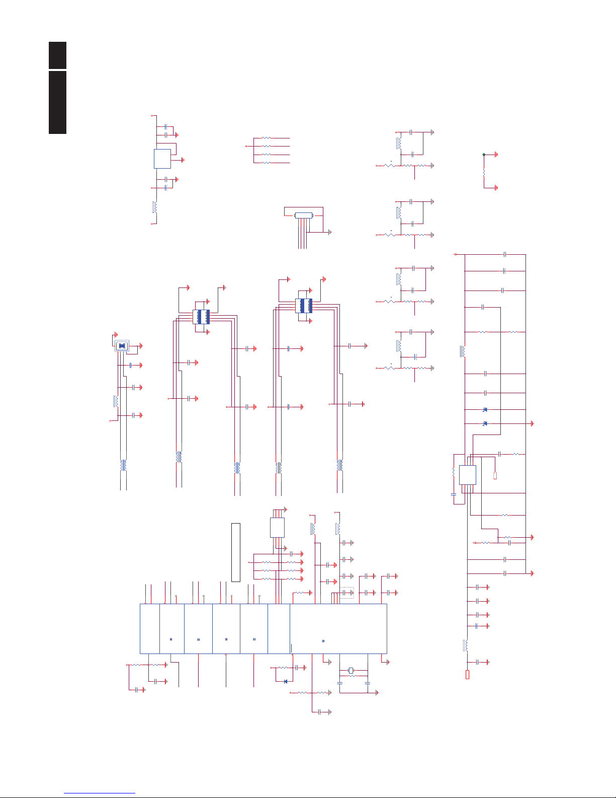
26
Meridian 3
Scaler Board (715G5774M1A000004S) (Only for 240P4QPYE)
Remark: Parts position can be searched by using FIND function in PDF.
ESD_5V
R105 1K C105 22N 25V
V5A
V5A
D102
BAT54C
3
1
2
DAT1-
DDC_WP
DVI5V
DAT1+
DAT0-
SCL_VGA
C102 47N16VR102 22 OHM 1/16W
R133 10 OHM
R135 10 OHM
RED-
R138 10 OHM
GREEN-
BLUE-
R111 100OHM
R137 10 OHM
R10675R 1/16W 1%
R110 100OHM
R141 10 OHM
ZD102
RLZ5.6B
1 2
HPD
R140 10 OHM
R136 10 OHM
R114 100OHM
DET_VGA
SCL_DVI
R134 10 OHM
DET_DVI
RIN 5
GNDR 5
VSYNC 5
BIN 5
GIN 5
R112
NC/1M 1/ 16W 5%
R139 120R 0.3A
12
DET_VGAI 5
HSYNC 5
GNDB 5
GNDG 5
R115 100OHM
SOG 5
RX1- 5
RX0- 5
RX1+ 5
DVI_SDA5
DDCA_SCL5
DDCA_SDA5
RX2+ 5
RX0+ 5
RXC- 5
RXC+ 5
DVI5V
VGA5V
RED+
DVI_SCL5
DDC_WP 5
DDC_WP 5
HSI
U101
CAT24C02WI-GT3A
A01A12A2
3
GND
4
SDA5SCL6WP7VCC
8
U103
CAT2 4C 02WI -GT3A
A01A12A2
3
GND
4
SDA5SCL6WP7VCC
8
DET_DVI
C118
220N 10V
R122
4.7K1/16W
C116
220N 10V
RX2- 5
DAT0+
GREEN+
R121 4.7K1/16W
R120 4.7K1/16W
R124 47R 1/16W 5%
R130 4.7K1/16W
R123 47R 1/16W 5%
R131 4.7K1/16W
DDC_WP
U109
AZC398-04S
I/O11GND2I/O2
3
I/O3
4
NC
5
I/O4
6
R119
2.2K1/16W
R118
2.2K1/16W
R116 100OHM
C1075PF 50V
C1085PF 50V
DAT2-
DAT2+
C1065PF 50V
R113 100OHM
ZD101
RLZ5.6B
1 2
R109
NC/ 22K 1/ 16W 5%
R108
NC/ 22K 1/ 16W 5%
VSI
DCLK+
DCLK-
FB101 19R 0.5A
1 2
FB103 19R 0.5A
1 2
FB102 19R 0.5A
1 2
FB104 120R
R127 1K
CN101
DB15
162738495
1112131415
10
1716
DET_DVII 5
R129
NC
R125 47R 1/ 16W 5%
DET_VGA
SDA_DVI
ESD_VGA
VGA5V
D101
BAT54C
3
1
2
CN102
JACK
DAT2-
1
DAT2+
2
2/4shield
3
DAT4-
4
DAT4+
5
DDC SCL
6
DDC SDA
7
VSYNC
8
DAT1-
9
DAT1+
10
1/3shield
11
DAT3-
12
DAT3+
13
+5V
14
SYNC GN D
15
HPD
16
DAT0-
17
DAT0+
18
0/5shield
19
DAT5-
20
DAT5+
21
clk shield
22
clk+
23
clk-
24
GND
26
GND
25
GND
27
GND
28
U110
AZC398-04S
I/O11GND2I/O2
3
I/O3
4
NC
5
I/O4
6
U102
AZC398-04S
I/O11GND2I/O2
3
I/O3
4
NC
5
I/O4
6
U104
AZC398-04S
I/O11GND2I/O2
3
I/O3
4
NC
5
I/O4
6
U105
AZC398-04S
I/O11GND2I/O2
3
I/O3
4
NC
5
I/O4
6
ZD103
NC/RLZ5.6B
ZD104
NC/RLZ5.6B
C115
22P 50V
ESD_DVI
C117
100N 16V
SDA_VGA
R128
NC/ 4K7 1 / 16W 5%
DVI_HPD 5
R101
75R 1/16W 1%
R10775R 1/16W 1%
R103 22 OHM 1/16W
R104 22 OHM 1/16W
R163
NC/75R 1/16W 1%
R162
NC/75R 1/16W 1%
R164
NC/75R 1/16W 1%
C114
22P 50V
BLUE+
R126 47R 1/16W 5%
R132
4.7K1/16W
C103 47N16V
C104 47N16V
C109 47N16V
C110 47N16V
C111 47N16V
ESD_5V
ESD_5V
R117 100OHM1/16W
INPUT

27
Meridian 3
Remark: Parts position can be searched by using FIND function in PDF.
R159
1K
DP_SINK_ASS_2 5
DP_SINK_ASS_1 5
U108
AZC398-04S
I/O11GND2I/O2
3
I/O3
4
NC
5
I/O4
6
R165
100K1/16W
R161
NC/ 10K 1/ 16W 5%
R167 0R05 1/16W
R168 0R05 1/16W
DP_VDD
need to layer
Differential Trace
CN103
DP CONN
SHELL1
21
SHELL2
22
ML_ Lane 3(n)
1
GND
2
ML_ Lane 3(p)3ML_ Lane 2(n)
4
GND
5
ML_ Lane 2(p)6ML_ Lane 1(n)
7
GND
8
ML_ Lane 1(p)9ML_ Lane 0(n)
10
GND
11
ML_ Lane 0(p)
12
GND13GND
14
AUX_CH(p)
15
GND
16
AUX_CH(n)
17
Hot Plug Detect
18
Return
19
SHELL4
24
SHELL3
23
DP_PWR
20
R156 0R05 OHM
DP_VDD
AUX_CHP 5
AUX_CHN 5
DP_HOT_PLUG 5
AUX_CHP
DP_VDD
ZD105
NC/RLZ5.6B
1 2
DP_VDD
LANE3P
LANE3N
LANE2P
LANE2N
LANE1P
LANE1N
LANE0N
LANE0P
R151
1M 1/16W
R152
NC
AUX_CHN
R154 0R 05 OH M
t
F101
PTCR
1 2
V33S-DP7
U107
AOZ8804DI
CH11CH22VN3CH34CH4
5
NC6NC
7
VN
8
NC9NC
10
LANE0P
LANE0N
LANE1P
LANE1N
LANE2N
LANE2PLANE2P
LANE3P
LANE3N
DP_VDD
R166
NC/ 0R 05 1/16W
U106
AOZ8804DI
CH11CH22VN3CH34CH4
5
NC6NC
7
VN
8
NC9NC
10
C122
100N 16V
R153 1K
R157
NC
R158
1M 1/16W
DET_DP 5
R150 100OHM
LANE2N
LANE2P
LANE0P
LANE3N
LANE0N
LANE3P
LANE1P
LANE1N
LANE0P 5
LANE0N 5
LANE3P 5
LANE3N 5
LANE1P
LANE0N
LANE1N
LANE0P
LANE2N 5
LANE1N 5
LANE2P 5
LANE1P 5
LANE3P
LANE2P
LANE3N
LANE2N
C120
100N 16V
DISPLAY PORT
!
28
Meridian 3
Remark: Parts position can be searched by using FIND function in PDF.
R436 0R05 OHM
CN402,CN403 BOTH LAYOUT
Pin 118
PW ON Latch:
Internal MCU :Pull High
External MCU :Pull Low
POWER
C443
10UF 10V
V12C
V33SDRAM
R482 100OH M
WP_PRO
DDC_WP 3
R439
NC/22K 1/16W 5%
C404
100N 16V
R418
4.7K1/16W
on_BACKLIGHT7
+
C423
NC/10UF50V
+
C418
100UF 16V
PS_ON7
PWM4
CN401
NC/CONN
12345
DVI_HPD3
AOUT_R1
V33TMDS
Adj_BACKLIGHT7
CN402
CONN
1234567891011
12
PANEL12V_ON7
DP_HOT_PLUG4
X401
14.31818MHZ/32PF
12
R422 NC
R423 NC
C420 1uF 10V
KEY2
LED_1
AUDIO_5V8
LED_2
V33TMDS
CN403
NC/CONN
12345
6
R430 100OH M
V33SDRAM
AOUT_L1
R431 100OH M
V33LSADC
R425
10K
V33CRYSTAL
KEY1
KEY2
FB407 120R
PA0
PA1
V12ADC
PA2
R416 560R 1/16W 5%
Mute 8
Mute
PA3
+
C403
100UF 16V
R435
0R05 OHM
PA4
R437
0R05 OHM
C427
NC/1N 50V
FB401 120R
DVI_SDA3
DVI_SCL3
PA6
PA5
PA7
R407 0R 05 OH M
R408 0R 05 OH M
R417
NC/1M 1/16W 5%
PS_DISTANCE
FB406 120R
DET_DP 4
PA8
PA9
DET_DP
PB0
PB1
PB2
R411
NC
R412
10K
C409
220N 10V
PB3
VCC3.3
WP
SDOUTCESDIN
R41422R 1/16W 5%
R41522R 1/16W 5%
R41322R 1/16W 5%
R440
47K 1/16W 5%
PB4
PB5
GNDG 3
SOG 3
GNDR 3
RIN 3
HSYNC 3
GIN 3
GNDB 3
BIN 3
VSYNC 3
+
C417
NC/100UF 16V
Audio_SD 8
XO
PB6
PB7
PB9
PB8
R404
4K7 1/16W 5%
R424
10K
LED driver
C401
220N 10V
R402 4.7K1/16W
C428
NC/1N 50V
R403 4.7K1/16W
PA[0..9] 6
V33P
TO Processor Board
PB[0..9]6
CLK
RX2+ 3
RX1+ 3
RX2- 3
RX0- 3
C440
10UF 10V
RX1- 3
RXC- 3
RX0+ 3
RXC+ 3
C441
100N 16V
VCC3.3
PIVOT_EN
VCC3.3
OC_SW
R455
100R 1/10W 5%
Q466
LMBT3904LT1G
C435100N 16V
R453
10K 1/16W 5%
OC401
RBS311115
4 3
1 2
Q402
LMBT3906LT1G
R456
4.7K1/16W
R445
NC/10K
WP_PRO
C442
100N 16V
R474
NC
C434100N 16V
ZD401
RLZ5.6B
1 2
LED_A
R444 NC/100OHM
LED_A
R463
NC
R447NC
LED_1
R473
56 OHM +-5% 1/8W
LED_2
R490
0R05 OHM
R443 NC/100OHM
R472
0R05 OHM
V5A
C410
NC/10pF 16V
V5A
LANE1P4
LANE3P4
C421
100N 16V
R406
0R05 OHM
LANE0P4
LANE2N4
LANE0N4
LANE2P4
LANE1N4
WP
LANE3N4
DET_DVII
DET_VGAI
DET_DP
ZD402
RLZ5.6B
1 2
R467
10K
R448NC
C433NC
C407 100N 16V
AUX_CHP4
C430
NC
EESCLEE_SCL
R4503.9K1/16W
R465
NC
R410 1K
C432NC
EESDAEE_SDA
R464
NC
C431NC
Q401
LMBT3906LT1G
R470
NC
R471
NC
R462 0R05 OHM
R460
10K
R4513.9K1/ 16W
R446
NC/10K
R426 0R 05 OH M
DDCA_SDA 3
R469
22K1/16W
R427 0R 05 OH M
DDCA_SCL 3
ZD403
RLZ5.6B
1 2
R4523.9K1/16W
R466
1 OHM +-5% 1/8W
R475
0R05OHM1/8W
R461
22K1/16W
R449NC
R468
NC
PWM1
PWM2
C419100N 16V
C438100N 16V
R486 0R05 OHM
VCC3.3
VCC3.3
VCC3.3
VCC3.3
AOUT_L1
C406 100N 16V
AUX_CHN4
AOUT_R1
AIN_R 8
AIN_L 8
AOUT_L 8
AOUT_R 8
R420
6.2KOHM 5% 1/16W
R405
100OHM
DP_SINK_ASS_2 4
ERGO_ON
FB408
120R
12
R401
100OHM
UART_TXD
UART_RXD
P53
ERGO_ON
PS_OUTPUT
PS_DISTANCE
R421
NC
P52
LED_G
LED_A
+
C422
100UF 16V
C416
100N 16V
DDCA_SCL 3
DDCA_SDA 3
C425
100N 16V
R433 NC
R434 NC
+
C408
NC/10UF16V
U403
M24C16
A01A12A2
3
GND
4
SDA5SCL6WP7VCC
8
U402
MX25L4006EM1I-12G
CE#
1
SO
2
WP#
3
GND
4
VDD8HOLD#7SCK6SI
5
VCC3.3
R409
4.7K1/16W
P53
+
C424
NC/10UF50V
P52
R457100K1/16W
C439
NC/1N 50V
C426
NC/1N 50V
EESCL
VCC3.3
EESDA
Near to scalar
DET_VGAI
R441
47K 1/16W 5%
DET_VGAI 3
DET_DVII 3
DET_DVII
R442
47K 1/16W 5%
VCC3.3
VCC3.3
VCC3.3
on_Panel7
POWER
LED_G
C414
100N 16V
V5A
V5A
V5A
R432
NC/10K 1/16W 5%
U401
RTD2486T D-GR
DP_VDD/TMDS_VDD
1
TMDS_REXT
2
LANE0P/RX2P_0
3
LANE0N/RX2N_0
4
LANE1P/RX1P_0
5
LANE1N/RX1N_0
6
LANE2P/RX0P_0
7
LANE2N/RX0N_0
8
LANE3P/RXCP_0
9
LANE3N/RXCN_0
10
DP_GND/TMDS_GND
11
LANE0P/RX2P_1
12
LANE0N/RX2N_1
13
LANE1P/RX1P_1
14
LANE1N/RX1N_1
15
LANE2P/RX0P_1
16
LANE2N/RX0N_1
17
LANE3P/RXCP_1
18
LANE3N/RXCN_1
19
DP_VDD/TMDS_VDD2
20
AVS0
21
AHS0
22
ADC_VDD
23
B0-
24
B0+
25
G0-
26
G0+
27
SOG0
28
R0-
29
R0+
30
GPI/GPO/V8_7
31
GPI/GPO / V8_6
32
ADC_GND
38
GPI/GPO/V8_1
37
GPI/GPO/V8_2
36
GPI/GPO / V8_3
35
GPI/GPO / V8_4
34
GPI/GPO/ V8_5
33
AUDIO_SOUTL/ V8_3/SCK/G PIO
45
SPDIF3/AUDIO_REF/V8_4/WS/GPIO
44
A-ADC0/VCLK/GPIO
50
A-ADC1/GPI O51A-ADC2/GPI O52A-ADC3/GPI O53A-ADC4/GPI O
54
TCON[0][5]/BADC0/PWM1/PWM5/GPIO
55
TCON[1][4]/B-ADC1/IICSCL/GPIO
56
V8_7/GPIO
41
TCON[9][11]/B-ADC2/IICSDA/GPIO
57
TCON[7][10]/DDCSCL1/GPIO
58
TCON[3][5]/DDCSDA1/GPIO
59
VCCK
60
PGND
61
PVCC
62
TCON[1][8]/PWM2/GPIO
63
SD0/SPDIF0/TCON[0][7]/GPIO/IrDA
64
AUDIO_HOUTL/V8_1/SD0/GPIO
47
AUDIO_HOUTR/V8 _0/PWM0/GPIO
48
ABLU7/SCK/TCON[4][2]/GPIO/BB3N
66
ABLU6/MCK/TCON[5][9]/GPIO/BB2P
67
ABLU5/SD0/SPDIF0/TCON[13][3]/GPIO/BB2N
68
LINE_INL/V8_6/IICSCL/GPIO
42
ABLU4/SPDIF1/SD1/TCON[ 7][3]/GPIO/IICSCL/BB1P
69
ABLU3/SPDIF2/SD2/TCON[ 9][11]/GPIO/IICSDA/BB1N
70
ABLU2/SPDIF3/SD3/TCON[10][8]/GPIO/PWM1/PWM5/BCLKP
71
TCON[6][12]/GPIO/PWM3/BCLKN
72
VCCK
73
ABLU1/ GPIO/ABLU7/ T XO3+_8b/TXO4+_10b/BG3P
74
ABLU0/ GPIO/ABLU6/TXO3-_8b/TXO4-_10b/BG3N
75
AGRN7/GPI O/ABLU5/T XOC+_8b/TXO3 +_10b/BG2P
76
AGRN6/GPIO/ABLU 4/TXOC-_8b/TXO3-_ 10b/BG2N
77
AUDIO_SOUTR/V8_2/MCK/GPIO
46
PVCC
84
PGND
85
ARED7/AGRN3/TXE3+_8b/TXO0+_10b/BR1P
86
LINE_INR/V8_5/ IICSDA/GPI O
43
GPIO/PWM3/TCON[11][6]/TXE0-_10b/AG2N
99
GPIOVCLK
40
LS_ADC_VDD
49
MCK/TCON[7]/GPIO/AR1P
108
GPIO/V8_0/
39
XO
127XI128
WS/TCON[7][1]/GPIO/PWM1/BB3P
65
AGRN5/GPIO/ABLU 3/TXO2+_8b/TXOC+_10b/ BG1P
78
AGRN4/GPIO/ABLU2/TXO2-_8b/TXOC-_10b/BG1N
79
AGRN3/GPI O/AGRN7/ TXO1+_8b/TXO 2+_10b/BR3P
80
AGRN2/GPIO/AGR N6/TXO1-_8b/TXO2-_ 10b/BR3N
81
AGRN1/GPI O/AGRN5/ TXO0+_8b/TXO 1+_10b/BR2P
82
AGRN0/GPIO/AGR N4/TXO0-_8b/TXO1-_ 10b/BR2N
83
ARED6/AGRN2/ TXE3-_8b/TXO0-_10b/BR 1N
87
ARED5/ARE D7/TXEC+_8 b/TXE4+_10b/A B3P
88
ARED4/ARED6/TXEC-_8b/TXE4+_10b/AB3N
89
ARED3/ARED5/ TXE2+_8b/TXE3+_10b/AB2P
90
ARED2/ARED4/ TXE2-_8b/TXE3-_10b/AB2N
91
ARED1/ARED3/ TXE1+_8b/TXEC+_10b/AB1P
92
ARED0/ARED2/ TXE1-_8b/TXEC-_10b/ AB1N
93
DENA/TXE0+_8b/T XE2+_10b/ACLKP
94
DHS/TXE0-_8b/T XE2-_10b/ACLKN
95
DCLK/GPIO/PW M0/TXE1+_10b/AG3P
96
DVS/GPIO/PWM 1/TXE1-_10b/AG3N
97
GPIO/PWM2/TX E0+_10b/AG2P
98
GPIO/PWM4/TCON[12][3]/AG1P
100
GPIO/PWM5/TCON[0]/AG1N
101
SD3/ SPDIF3/TCON[10]/GPIO/PWM0/AR3P
102
SD2/SPDIF2/TCON[8]/GPIO/IICSCL/PWM1/AR3N
103
SD1/SPDIF1/TCON[5]/GPIO/I RQ/IICSDA/AR2P
104
SD0 / SPDIF0 / TCON[9] / GPIO / AR2N
105
PVCC
106
PGND
107
SCK/TCON[3]/GPIO/AR1N
109
WS/TCON[6]/GPIO/SDT
110
SD0/SPDIF0/TCON[4]/GPIO/SPDIF1
111
SD1/ SPDIF1/TCON[9]/GPIO/WS
112
SD2/SPDIF2/TCON[1][11]/GPIO/IrDA/SCK
113
SD3/SPDIF3/TCON[13]/GPIO/VC LK/ MCK
114
SPI_SCLK/SeriesData
115
SI/MCU_SCLK
116
SO/SCSB
117
CEB/IRQB
118
GPIO/PWM5/SPDIF1
119
VCCK
120
DDCSCL3/GPIO/AUX-CH_P1
121
DDCSDA3/ GPIO/AUX-CH _N1
122
DDCSCL2/GPIO/AUX-CH_P0
124
DDCSDA2/ GPIO/AUX-CH _N0
123
RESETB
125
CEC/GPIO/PWM1/SPDIF2
126
E-Pad
129
V33SDRAM
OC_SW
SDOUT
CLKCESDIN
PIVOT_EN
on_Panel
R458
10K
CE
V33CRYSTAL
DP_SINK_ASS_1 4
V33TMDS
V12C
R428 NC
R429 NC
DC POWER SAVING9
XI
Volume
V33P
XO
Volume 8
PS_OUTPUT
UART_TXD
UART_RXD
C405
100N 16V
KEY1
KEY2
For Auto Pivot Function
R438
NC/22K 1/16W 5%
C411
22P 50V
V12S7
V12CV12S
V33S7
VCC3.3 V33P
R419
NC/4K7 1/16W 5%
V12ADC
C412
22P 50V
V12C
V33LSADC
KEY1
ERGO_ON
FB402 120R
V33P
FB405 120R
FB403 120R
V33P
FB404 120R
XI
SCALER
29
Meridian 3
Remark: Parts position can be searched by using FIND function in PDF.
C437
100N 16V
C429,C431 lay
ǂ
LVB1PPB6
LVB2MPB5
LVB1MPB7
LVB3MPB1
LVB3PPB0
LVBCKPPB2
LVBCKMPB3
LVB2PPB4
PB[0..9]
FB409
120R 6A
1 2
R4811.5K 1/4W
CN408
CONN
246810
12
14
16
18
20
22
24
26
28
30
13579
11
13
15
17
19
21
23
25
27
29
CN407
NC/CONN
123456789
10
11
12
13
14
15
16
17
18
19
20
21
22
23
24
25
26
27
28
29
30
LVB0PPB8
LVB0MPB9
RXO0- RXO0+
RXO1- RXO1+
R4801.5K 1/4W
RXO2-
PA6 LVA1P
PA5 LVA2M
RXO2+
PA0 LVA3P
PA4 LVA2P
PA3 LVACKM
PA1 LVA3M
PA7 LVA1M
PA[0..9]
RXOC-
PA8 LVA0P
RXOC+
RXO3- RXO3+
RXE0-
PB[0..9]5PA[0..9]5
RXE0+
VLCD 7
VLCD
RXE1- RXE1+
RXE2- RXE2+
RXEC- RXEC+
option
RXE3- RXE3+
PA9 LVA0M
LVA0P RXE0+
PA2 LVACKP
RXE3-LVA3M
RXO3-LVB3M
RXE2-LVA2M
RXE1-LVA1M
LVB2M RXO 2-
RXO1-LVB1M
RXO0-LVB0M
LVACKM RXEC-
LVBCKM RXOC-
RXE0-LVA0M
RXOC+LVBCKP
RXO0+LVB0P
RXE2+LVA2P
RXO1+LVB1P
RXEC+LVACKP
RXO3+LVB3P
RXO2+LVB2P
RXE1+LVA1P
RXE3+LVA3P
+
C436
NC/150uF/25V
PANEL INTERFACE
!
30
Meridian 3
Remark: Parts position can be searched by using FIND function in PDF.
Scaler Core
Adj_BACKLIGHT 5
on_BACKLIGHT 5
PANEL12V_ON5
V5A
V5A R731
10K
BKLT_EN
C726
10N 50V
FB702
120R 6A
L702
22uH
FB704
120R 6A
R721
10K 1/10W 5%
R724
4K7 1/10W 5%
FB703
120R 6A
R717
10K 1/16W
R715
4.7K1/16W
+16V
C720
10UF 25V
C724
100NF 25V
V5A
C714
100NF 25V
D703
SX36
1 2
R720
0R05 OHM
C715
1uF 25V
R722
10 OHM
C719
22P 50V
+
C727
470UF 10V
R723
14.7KOHM 1/10W
+
C730
150uF/25V
R728 24K 1/16W 5%
U703
AT1528P11U
VCC1REF2GND3FB
4
EN
5
PGND
6
LX
7
VIN
8
R726
10K
C713
100NF 25V
R714
30Kohm 1/16W +/-5%
Q705
NC/AO3401
C718
220PF 50V
Q704
LMBT3904LT1G
C723
100NF 25V
C716
1uF 25V
C728
100N 16V
C729
0.47uF 16V
C725
10UF 10V
C712
10UF 25V
D705
NC/LL4148
+
C722
150uF/25V
R727
10K
VLCD
VLCD 6
on_Panel5
R716
10K
H: OnL:Off
C721
10UF 25V
TCON POWER
+3.3V_SW
+3.3V
GND
GND
GND
C711
10UF 25V
Q706
AO4411
S
1
S
2
S
3
G
4
D
8
D
7
D
6
D
5
+3.3V_SW
+
C710
150uF/25V
R729
NC/47K 1/16W 5%
FB701
48R 6A
1 2
C717
820pF 50V
R730
10K
D704
SX36
1 2
R713 N C/100K1/16W
U702
APW7089KAI-TRG
VIN1EN2UGND3VCC
4
LX
5
COMP
6
FB
7
GND
8
LX
9
GND
GND
R719
10K +-1% 1/16W
+12V_Panel
+12V_Panel
+12V_Panel
L701
10uH 20%
BKLT_ADJ
R718
140K 1%
AT1528P11U: Max:2A
Vout = 0.8V (1+(ĴR1/R2 ))
Cancel U705
V33S
V33S 5
V33S-DP 4
+16V
R701
100R 1/10W 5%
PS_ON1
BKLT_ADJ
R703
10K 1/10W 5%
+
C701
150uF/25V
BKLT_EN
R706
NC/0R05 OHM
U701
G912PT43U
VOUT
2
VIN
3
GND
1
CN701
CONN
1234567891011
12
D701
SR34H
1 2
D702
SR34H
1 2
V5A 3,5,8
V5A
+16V 9
+
C703
220UF 16V
C702
1N 50V
(1)LGD LM240WU8-SLD1 (12V):
R717=10K;R718=140K
(2)SEC LTM240CL01(5V):
R717=12.1K;R718=63.4K
need to adj 3.3V
R702
10K 1/10W 5%
R705
220ohm 1/16W +/-1%
V33S
R709
NC
R712
0R05 1/10W
PS_ON 5
C707
100N 16V
C705
100N 16V
+
C706
100UF 16V
R708
10K 1/10W 5%
R704
NC
R710
100OHM
R711
0R05 OHM
C708
100N 16V
Q701
LMBT3904LT1G
R709->0ohm
R701->0ohm
R706 ->100ohm
Q1 NC
Q702
NC/LMBT3904LT1G
C709
100P 50V
+
C704
100UF 16V
R707 22K1/16W
V12S 5
GND
V33S
V12S
V33S
V33S V5A
POWER

31
Meridian 3
Remark: Parts position can be searched by using FIND function in PDF.
C608
100N 16V
OUT-L-
Earphone_Det
Headset_R
OUT-R+
VCC_IN
Headset_L
OUT-R-
OUT-L+
R614
10K
AA4
Q601
AO3401A
OUTR
OUTL
FB606 120R 6A
1 2
C605330PF 50V
R628
100OHM
C623 NC
R603
10K
SE-1
Q602
LMBT3906LT1G
1
23
C618
0.47uF 16V
R627
0R05 OHM
+
C612
100UF 16V
SE
R632
NC
R607
10K
R624
33K 1/16W
C604 1UF 16V
FB601
120R 6A
1 2
C616
10UF 10V
R606
1K
FB602
120R 6A
12
C626
1UF 16V
R619 200R 1/ 10W 5%
C622
1UF 16V
R626
0R05 OHM
+
C601
220UF 16V
C602
100N 16V
R64033K 1/16W
R618
100K1/16W
Heat Sink = Q90G6119 4
R605
10K
R601
100OHM
C619
NC
Q603
LMBT3904LT 1G
C624
0.47uF 16V
C625
100N 16V
C631
1NF 50V
R602
10K
R611
10K
R621 200R 1/ 10W 5%
R609
10K
R610
10K
C603 1UF 16V
R613 0R 05 1/10W
R631
0R05 1/10W
R608
470OHM1/16W
FB605 120R 6A
1 2
+
C620
220UF 16V
R630
NC
C628
1NF 50V
+
C621
220UF 16V
FB603 120R 6A
1 2
R620 100K1/16W
R623
1K
R629
100OHM
CN601
PHONE JACK
12354
R625
NC
R612 0R 05 1/10W
C617
1UF 16V
C610
1UF 16V
R616
1K
C630
1NF 50V
R622
3K1/16W
D601
LL4148
C615
1UF 16V
R64133K 1/16W
C614
1UF 16V
C629
1NF 50V
C627
10UF 10V
C613
100N 16V
C606330PF 50V
FB604 120R 6A
1 2
U601
APA2606NAI-TRG
LOUTP
1
PGND
2
PGND
3
LOUTN
4
PVDD
5
MUTE
6
VDD
7
LINN
8
UVP
9
VDC
10
VOLUME
11
HP_LOUT
12
HP_ROUT
13
BYPASS
14
SE/BTL
15
AGC
16
RINN
17
GND
18
SD
19
PVDD
20
ROUTN
21
PGND
22
PGND
23
ROUTP
24
Ther n a l Pad
25
V5A3,5,7
+5V_AUDIO
+5V_AUDIO
+5V_AUDIO
+5V_AUDIO
+5V_AUDIO
V5A
+5V_AUDIO
+5V_AUDIO
+5V_AUDIO
+5V_AUDIO
+5V_AUDIO
C607
100N 16V
Headset_L
C609
100N 16V
Headset_R
Earphone_Det
Mute5
AOUT_L5
AIN_L 5
AOUT_R5
AIN_R 5
OUT-R+
CN602
CONN
123456789
MUTE-1
OUT-L-
G-2
OUT-R-
UVP
G3
OUT-L+
AUDIO_5V
VCC_IN
MUTE-1
G-1
Volume5
AUDIO_5V 5
UVP
C632
NC/330pF 50V
R633
NC/10 OHM
AA1
VOL
OUTR
SE
C633
NC/330pF 50V
R634
NC/10 OHM
Audio_SD5
C634
NC/330pF 50V
R636
NC/10 OHM
R635
NC/10 OHM
C635
NC/330pF 50V
AA2
AA3
AA4
MUTE
AA1
R617
100OHM
R604
10K
C611
100N 16V
VOL
+5V_AUDIO
MUTE-1
AA2
OUTL
AA3
AUDIO

!
32
Meridian 3
Remark: Parts position can be searched by using FIND function in PDF.
/OC2
/OC1
DP2
DM2
/OC1
VBUS1A
DM44
C542
1N 50V
C539
1N 50V
UGND
UGND
FB507
120R 0.3A
1 2
/OC3
VBUS_DET
C528
1N 50V
C529
1N 50V
UGNDUGND
2A
/OC2
Power Regulator
CN501
NC/CONN
12345
67
Layout Note
C530
100N 16V
DP0
Disable Downstream 4
VBUS0
UGND
12
34
CN504
CONN
123
4
6 5
DM / DP pair to p a i r
б
35mil
DM0
UGND
DM4
UGND
DP4
U802 Decoupl ing
ㆯ⭗ى㏬
IC
б
DM / DP :7
mils
DM / DP Trac e
䭓
à
ǂǂ
70
ǂ
DM / DP Trace width 18 mils
Disable Downstream 3: R735, R736 pull high 10K
Disable Downstream 4: R737, R738 pull high 10K
UGNDUGND
EEPROM mount: R812~814 pull h i
MP158 4EN
U501
SW
1
EN
2
COMP
3
FB
4
GND5FREQ6VIN7BST8Therm al Pa d
9
/OC3
DC POWER SAVING5
EEPROM NC: R818~820 pull low
UGND
DM11
DP4
DP11DP1
DP44
DM1
DP3
DM3
DM4
1B
1A
1234
5678
CN503
USB CONN
1
2
3
4
6
5
7
8
11
12
9
10
DM1
DP1
DM2
DP2
VBUS2A
DM33
DP3
UGND
VBUS3
C535
100N 16V
L503
90R/400mA
1
2
4
3
UGND
DM3
DP33
VBUS3A
C536
1N 50V
UGND
R735
0R05
/OC4
C532
1N 50V
UGND
UGND
/OC4
VBUS4A
VBUS4
+16V7
DP44
DM44
UGND
DM2
UGND
DP2
L504
90R/400mA
1
2
4
3
VBUS2
DM22
C534
1N 50V
C533
100N 16V
UGND
DP22
UGND
C538
1N 50V
UGND
C504
10uF 25V
UGND
DP0
DM1
UGND
C505
10uF 25V
DP1
R507
10K
C503
10uF 25V
R505
68.1K 1%
R515
0R05 1/10W
+
C520
100UF 16V
C510
150pF 50V
R504
100K1/16W
R532
10K
R514
15K 1/16W
R522
100K1/16W
C526
100N 16V
FB505
120R 6A
1 2
FB501
120R 6A
1 2
C540
1uF 10V
R506
12.4K 1%
R526
11.5K +-1% 1/16W
C544
33P 50V
U503
NC/M24C02- WMN6TP
A01A12A2
3
GND
4
SDA5SCL6WP7VCC
8
D504
NC/LL4148
C517
100N 16V
C507
0.1uF 50V
C548
4.7UF
D502
SR34H
1 2
C586
1N 50V
C531
100N 16V
Ups tr ea m
Dow ns tr eam 1
Dow ns tr eam 2
Dow ns tr eam 3
Dow ns tr eam 4
EEPROM/ Co nf i g
Common
U502 USB2514B-AEZC
USBUP_DP
31
USBUP_DM
30
USBDN1_DP
2
USBDN2_DP
4
USBDN3_DP
7
USBDN4_DP
9
USBDN1_DM
1
USBDN2_DM
3
USBDN3_DM
6
USBDN4_DM
8
VBUS_DET
27
PRTPWR1
12
PRTPWR2
16
PRTPWR3
18
PRTPWR4
20
OCS_N[1]
13
OCS_N[2]
17
OCS_N[3]
19
OCS_N[4]
21
RBIAS
35
SDA/SMBDATA/NON_REM1
22
SCL/SMBCLK/ CFG_SEL0
24
HS_IND/CFG_SEL1
25
XTAL 1/ CL KI N
33
XTAL2/CLKIN_EN
32
RESET26LOCAL_PWR/NON_REM0/SUSP_IND28TEST
11
VDD33
23
PLLFILT
34
VDDA33
29
VDDA33/VDD33PLL
36
VDD33
15
CRFILT
14
VSS(FLAG)
37
VDDA335VDDA33
10
FB502
120R 6A
1 2
C519
100N 16V
+
C524
100UF 16V
FB509
120R 6A
1 2
t
F503
PTCR
12
C511
1N 50V
C537
100N 16V
R517
NC/10K
C554
100N 16V
C513
10uF 25V
t
F502
PTCR
12
C509
100N 16V
U504
AP1117E33L-13-77
ADJ(GND )
1
VOUT
2
VIN
3
4
4
L506
90R/400mA
1
2
4
3
R524
10K
R508
15K 1/16W
R531
NC
L501
22uH
R520
51K 1/16W 5%
R519
NC/10K
R512
15K 1/16W
R511
10K
C547
100N 16V
R523
NC
C501
0.1uF 50V
C550
100N 16V
R501
NC/10K 1/10W 5%
C555
NC
C551
100N 16V
R527
NC
FB503
120R 6A
1 2
DM0
C545
100N 16V
R513
10K
C506
0.1uF 50V
C512
1N 50V
X501
24.000MHZ
12
FB506
120R 6A
1 2
R530
10K
C508
0.1uF 50V
R518
NC/10K
C553
100N 16V
C521
100N 16V
R503
300K
+
C522
100UF 16V
+
C502
150UF 35V
FB508
120R 6A
1 2
C549
4.7UF
+
C514
470UF 10V
+
C518
100UF 16V
t
F504
PTCR
12
R525
1M 1/16W
D501
SR34H
1 2
C541
100N 16V
+
C527
100UF 16V
C543
33P 50V
R510
15K 1/16W
C546
4.7UF
R509
10K
R528
10K
R521
100K1/16W
+
C516
100UF 16V
R502
30K 1/10W 5%
t
F501
PTCR
12
R516
NC/10K
C525
100N 16V
R529
NC
C523
100N 16V
C515
100N 16V
FB504
120R 6A
1 2
C552
100N 16V
UGND
VBUS0
UGND UGND
UGNDUGND
UGND
U5V
L505
90R/400mA
1
2
4
3
VBUS1
UGND
UGND
UGND UGND
UGND
UGND
UGND
UGND
U5V
VBUS4
USB3.3V
UGND
UGND
UGND
UGND
VBUS0
UGND
VBUS4
UGND
UGND
UGND
UGND
UGND
USB3.3V
USB3.3V
VBUS2
UGND
UGND
USB3.3V
USB5V
USB3.3V
USB5V
VBUS3
UGND
UGND
UGNDUGND
L502
90R/400mA
1
2
4
3
UGND
UGND
UGND
UGND
UGND
UGND
USB5V
USB3.3V
UGND
UGND
UGND
UGND
UGND
VBUS1
USB5V USB5V
USB3.3V
UGNDUGND
UGND
1234
5678
CN502
USB CONN
1
2
3
4
6
5
7
8
11
12
9
10
UGND
UGND
UGND
2010/1/25
USB

33
Meridian 3
6.2 Power Board (715G5164P02002001M)
Remark: Parts position can be searched by using FIND function in PDF.
IC801
OZ9998AGN
PWM1ISEN12ISEN23ISEN34ISEN45GNDA6ISEN87ISEN68ISEN79OVP10ISET11RT
12
ENA
13
ISW
14
ISEN5
15
LDR
16
VREF
17
GNDP
18
VIN
19
SEL
20
COMP
21
SSTCMP
22
NC
23
STATUS
24
R851
0R05 1/10W
FB802
BEAD
1 2
CN803
NC
12345
R847
0R05 1/10W
R849
NC
+
C813
100uF
Q801
EMBA2N10A
R806
10K 1/10W 5%
Vout
R812
100R 1/10W 5%
C805
0.47uF 16V
R808
NC
R810
1K 1/10W 5%
C807
2U2 16V
JUMP/EMI
R824
47KOHM +-1% 1/10W
ZD801
NC/SK510B
R804 27K 1/10W 1%
R809
100K
C806
0.47UF 50V
C811
100PF 50V
R805
270K +-1% 1/8W
+16V
CN802
NC
12345
6
7 8
R801
0.3R 1/ 4W
FB803
BEAD
1 2
IS1
IS3
IS2
IS7
IS6
IS4
C812
100P 50V
R814
10R
IS8
IS5
L801
33UH
2
4
IS1
IS2
IS3
R848
1R 1/10W 5%
IS4 IS8IS7IS5 IS6
R850
1R 1/10W 5%
R852
1R 1/10W 5%
+
C804
4.7UF 100V
IO1 IO3IO2 IO4
R846
1R 1/10W 5%
C820
0.47UF 50V
C821
0.47UF 50V
FB801
NC
1 2
IO1
IO2
IO3
IO4
ZD802
SR5100
R844
10 OHM 1/4W
R822
1M 1/8W 5%
C815
330NF 16V
Vout
Vout
R842
RST 0603 18K 1% 1/10W
R845
100 OHM 1/4W
C814
680P 50V
CN801
CONN
246
135
R802
0.3R 1/ 4W
R813 10K 1/ 10W 5%
C801
0.1uF 50V
DIM
ON/OFF
OVP1
OVP1
R807
10R 1/10W 5%
IO2
IO1
IO3
IO4
Vout
CONVERTER
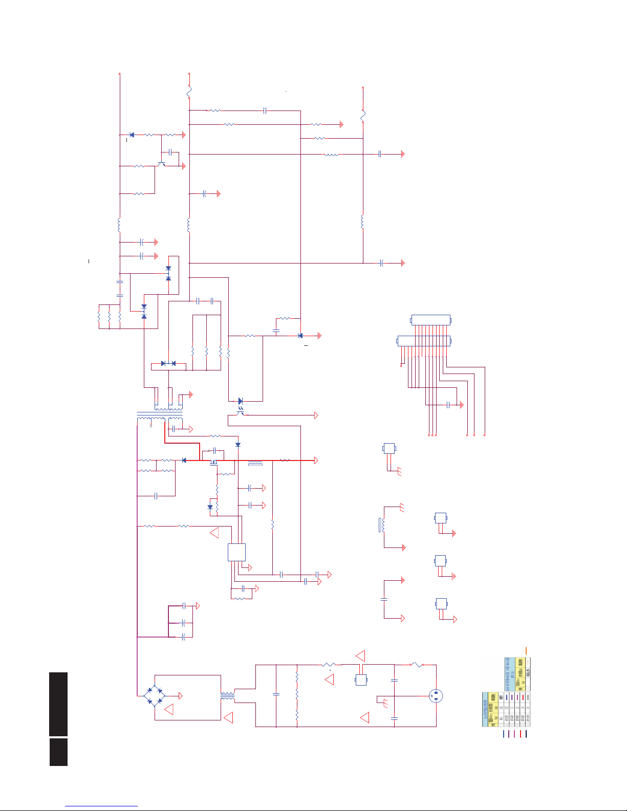
!
34
Meridian 3
Remark: Parts position can be searched by using FIND function in PDF.
C919
1000PF 50V
IC901
LD7750RGR
OTP1COMP2CS3GND
4
OUT
5
VCC
6
HV
8
C934
1N 50V
C922
1N 50V
L904
3.5uH
R917
220oHM
CN902
CONN
123456789
10
R932
100KOHM +-5% 1/8W
R908
10 K 1/4W
D902
FR107
D904
1N4148
C911
0.1uF 50V
R910
1 OHM 1/4W
R919
0.39R
C914
NC
C924
100N 50V
C906
1500PF2KV
R905
10 K 1/4W
R923
22 OHM 1/4W
F903
T4AL 250V
NC/F902
T4AL 250V
C921
330PF 500V
+
C905
100uF 450V
IC903
TL431G-A-TA
R913
100K
R914
100K
R907
100K
R906
100K
R927
10KOHM +-1% 1/8W
+5V
+16V
+5V
Q903
KTD1028
CN901
SOCKET
12
3
R962 47 OHM 1/4W
Audio_SD
R920
47 OHM 1/4W
FB902
BEAD
1 2
+5V1
!
T901
POWER X''F MR
54632
789
10
11
12
C910
2N2 500V
C929
2N2 500V
C935
2N2 500V
HV
R939
1K 1/8W
!
L903
3.5uH
F901
T4AL 250V
C931
100N 50V
C903
470NF
+
C913
47UF 50V
5V/2.5A
16V/2.35A
+
C915
470UF 16V
R943
470OHM +-5% 1/8W
C932
1N 50V
NC/D 907
SFF1004G
1
2
3
R925
2.2 KOHM +- 1% 1/8W
+
C916
1000UF 10V
HS2
HEAT SINK(D905)
1
2
HS3
HEAT SINK(D906)
1
2
C907
NC
R940
1K OHM
ZD902
GDZJ24B
C912
2N2 500V
D905
MBRF10100CT
1
2
3
C933
47nF 50V
R947
820R
R946
820R
-
+
BD901
KBJ408G
2
1
3
4
C920
47PF1KV
CN905
CONN
L
1
N
2
NC/C 930
100N 50V
D906
MBRF20200CT
1
2
3
NC/R933
20KOHM +-1% 1/8W
HS1
HEAT SINK
1
2
C901
0.001uF/250V
R902
680K 1/4W
DIM
+16V
NC/L905
3.5uH
GND
GND
1
2
C902
0.001uF/250V
!
ON/OFF
IC902
PS2561DL1-1
12
43
R924
820 OHM 1/4W
L901
30MH
1
2
4
3
!
R961 47 OHM 1/4W
R935 47 OHM 1/4W
+
C917
470UF 35V
C900
0.0022uF/250V
+
C905A
NC
VOL
R918
47 OHM 1/4W
R916
47 OHM 1/4W
R903
680K 1/4W
R926
2K 1/8W 1%
L906
NC
+
C918
470UF 35V
t
NR901
NTCR
12
R930
9K53 1/8W 1%
NC/CN903
CONN
123456789
1011121314
FB901
BEAD
1 2
MUTE
R901
680K 1/4W
R912
10K 1/4W
R911
22 OHM 1/4W
Q901
SMK0870F
!
D903
FR107
POWER
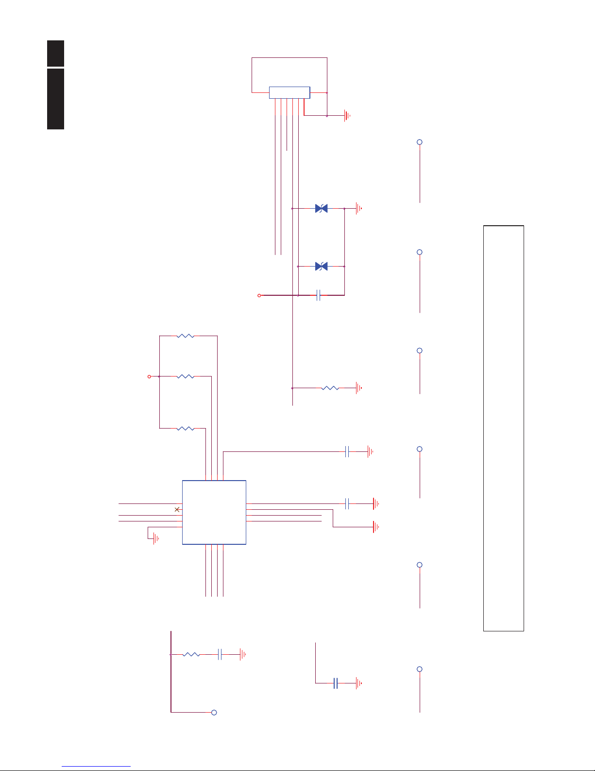
35
Meridian 3
6.3 Key Board (715G5446K01000004S)
Remark: Parts position can be searched by using FIND function in PDF.
SM_INT#
CIN_07
FFC R/A: 311GF100C06ADH
FFC V/T: 311GF100D06ACJ
FFC CABLE: 089G 76J 6 3
WIRE V/T: 033G8032 6F S HR
CIN_07
CIN_11
CIN_03
V3.3
R003
4.7K1/16W
R005
100OHM
R004
680OHM +-5% 1/10W
C004
100P 50V
MenuBrightness PowerSmartPower
GPIO_00
C003
100N 16V
CIN_01
SmartPowerBrightness
TP6 KEY0.1524
Menu
CIN_05
C001
100N 16V
Differential
C002
100N 16V
SmartImage
GPIO_00
SM_CLK
U001
IT7230EFN/BX
CIN031CIN072CIN093CIN11
4
VSHILD
5
VBIAS
6
AVSS
7
AVCC
8
DVCC
9
SCLK
10
SDA
11
INT#
12
GPIO0
13
GPIO1
14
CIN00
15
CIN01
16
E-PAD
17
ZD001
MLVS0603M04
12
CIN_09
SmartImage
CIN_03
SM_DATA
SM_INT#CIN_05
V3.3
V3.3
AC_SHIELD
VBIAS
Power
R001
10K
AC_SHIELD
CIN_01 CIN_09CIN_11
KEY0.1524
TP3
KEY0.1524
TP2
KEY0.1524
TP5
KEY0.1524
TP1
R002
4.7K1/16W
KEY0.1524
TP4
CN001
CONN
12345
6
78
KEY0.1524
TP7
VBIAS
ZD002
MLVS0603M04
12
SM_CLK CLK
C005
1UF 16V
V3.3
DATASM_DATA
Key Touchpad

!
36
Meridian 3
Key Board (715G6073K01000004S) (Only for 240P4QPYES)
Remark: Parts position can be searched by using FIND function in PDF.
SM_INT#
CIN_07
FFC R/A: 311GF100C06ADH
FFC V/T: 311GF100D06ACJ
FFC CABLE: 089G 76J 6 3
WIRE V/T: 033G8032 6F S HR
CIN_07
CIN_11
CIN_03
CN001
CONN
12345
6
78
R005
100OHM
R004
NC/680OHM +-5% 1/10W
C004
100P 50V
MenuBrightness PowerSmartPower
GPIO_00
C003
100N 16V
CIN_01
SmartPowerBrightness
TP6 KEY0.1524
Menu
CIN_05
C001
100N 16V
Differential
C002
100N 16V
SmartImage
GPIO_00
SM_CLK
U001
IT7230EFN/BX
CIN031CIN072CIN093CIN11
4
VSHILD
5
VBIAS
6
AVSS
7
AVCC
8
DVCC
9
SCLK
10
SDA
11
INT#
12
GPIO0
13
GPIO1
14
CIN00
15
CIN01
16
E-PAD
17
ZD001
MLVS0603M04
12
CIN_09
SmartImage
CIN_03
SM_DATA
SM_INT#CIN_05
V3.3
V3.3
AC_SHIELD
VBIAS
Power
AC_SHIELD
CIN_01 CIN_09CIN_11
KEY0.1524
TP3
KEY0.1524
TP2
KEY0.1524
TP5
KEY0.1524
TP1
KEY0.1524
TP4
KEY0.1524
TP7
VBIAS
ZD002
MLVS0603M04
12
SM_CLK CLK
C005
1UF 16V
V3.3
DATASM_DATA
Key Touchpad
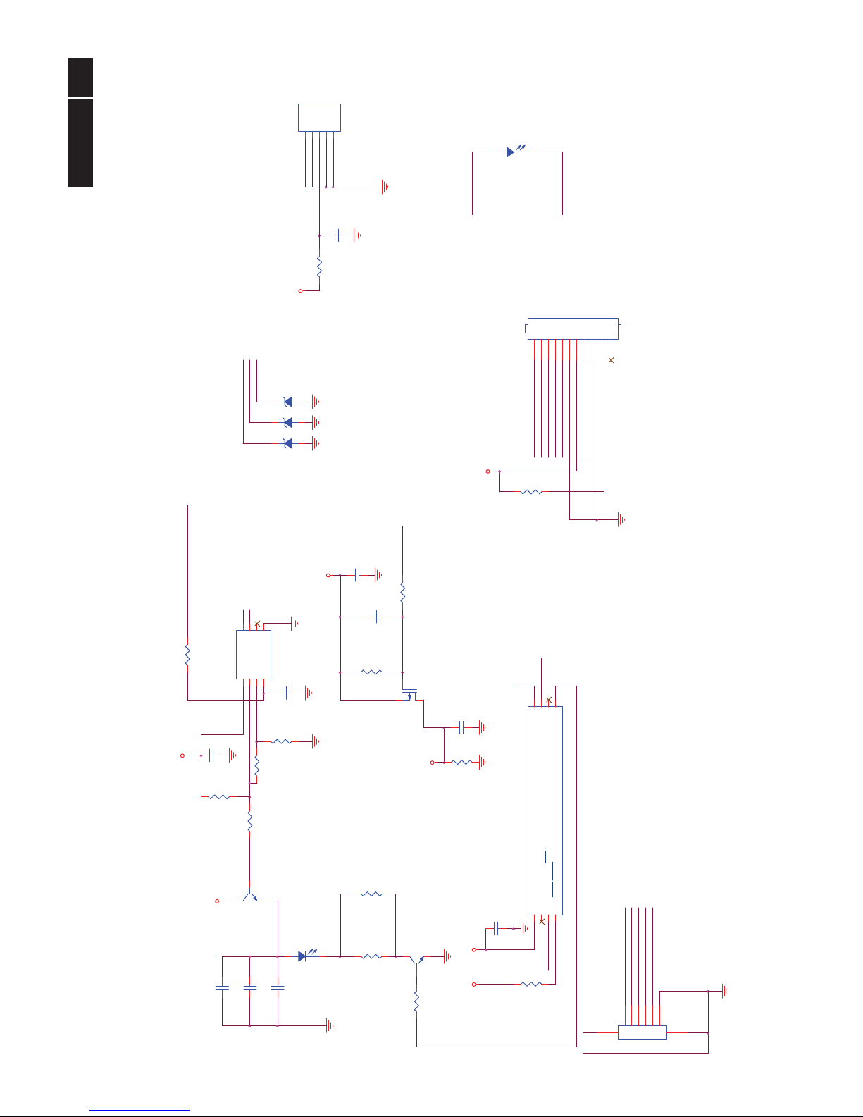
37
Meridian 3
6.4 IR Board (715G5459R01000004S)
Remark: Parts position can be searched by using FIND function in PDF.
IR_RX
PS_OUTPUT
VCC_IN
IR_RX
R/A: 081G 15W 1 EL
V/T: 081G 63W 2 GP
REVERSE: 081G 14 31 EL
FFC R/A: 311GF100C06ADH
FFC V/T: 311GF100D06ACJ
FFC CABLE: 089G 76J 6 3
WIRE V/T: 033G8032 6F S HR
FFC R/A: 311GF100C12ADH
FFC V/T: 311GF100D12ACJ
FFC CABLE: 395G076J12NM01
WIRE V/T: 033G803212F S HR
R313
NC/1K
C311
NC/100N 16V
C318
NC/ 100N 16 V
C316
NC/100N 16V
C312
NC/ 100 N 16V
C317
NC/100N 16V
R312
NC/100K1/16W
LED_VCC
PS_OUTPUT
C315
NC/100N 16V
CN311
CONN
12345
6
78
VCC_KB
R323
NC/10K
I2C_SDA
PS_ON
ZD312NC/UDZSNP5.6B
1 2
CN312
CONN
123456789
101112
PS_DISTANCE
I2C_SCL
SM_INT#
R315
NC/100K1/16W
C314 NC/22UF 16V
R320
NC/100OHM
R316
NC/100 OH M 1/8W
R311
NC/1K
U311
NC/AS358MTR-E1
1OUT
1
1IN-
2
1IN+
3
GND
4
2IN+52IN-62OUT7VCC+
8
R317
NC/33 OHM 1/8W
U313
NC/PIC12F615-I/SN
VDD1GP5/T1CKI/P1A*/OSC1/CLKIN2GP4/AN3/CIN1-/T1G/P1B*/OSC2/CLKOUT3GP3/T1G*/MCLR/VPP
4
GP2/AN2/T0CKI/INT/COUT/CCP1/P1A
5
GP1/AN1/CIN0-/VREF/ICSPCLK
6
GP0/AN0/CIN+/P1B/ICSPDAT
7
VSS
8
C313 NC/ 22U F 16V
ZD313NC/UDZSNP5.6B
1 2
R319
NC/1K
Q313
NC/AO3401A
C320
NC/100N 16V
R324
10K
R322
NC/10K
C319
NC/ 100N 16 V
Q312
NC/SST2222A
R314
NC/100K1/16W
U312
NC/IRM-3638M3S28
VOUT1GND2VCC3HAND14HAND2
5
R321
NC/1K
LED311
A8824B/IR204C-A
12
LED312
LED
12
ZD311NC/UDZSNP5.6B
1 2
R318
NC/ 33 OH M 1/ 8W
Q311
NC/SST2222A
VCC
VCCVCC
VCC_IN
VCC
VCC
VCC
VCC_IN
PS_ON
VCC_KB
LED_White
I2C_SCL
I2C_SDA
PS_ON
PS_OUTPUT
PS_DISTANCE
LED_VCC
PS_DISTANCE
LED_white
SM_INT#
POWER SENSOR_LED

!
38
Meridian 3
6.5 Head Phone Jack Board (715G5462T01000004Q) (Only for 240P4QPYES)
Remark: Parts position can be searched by using FIND function in PDF.
LOUT+
Headset_R
Earphone_Det
ROUT+
ROUT-
Headset_L
LOUT-
CN683
CONN
123
4
6 5
GND
CN681
CONN
123456789
1011
U681
AZ2025-04S
I/O1
1
GND
2
I/O23I/O3
4
I/O4
5
GND
LOUT+
LOUT-
ROUT+
ROUT-
Headset_R
U682
AZ2025-04S
I/O1
1
GND
2
I/O23I/O3
4
I/O4
5
GND
Headset_L
Earphone_Det
CN684
PHON E J AC K
12354
Headset_R
Headset_L
Ear-phone
GND
Earphone_Det
Head Phone Jack
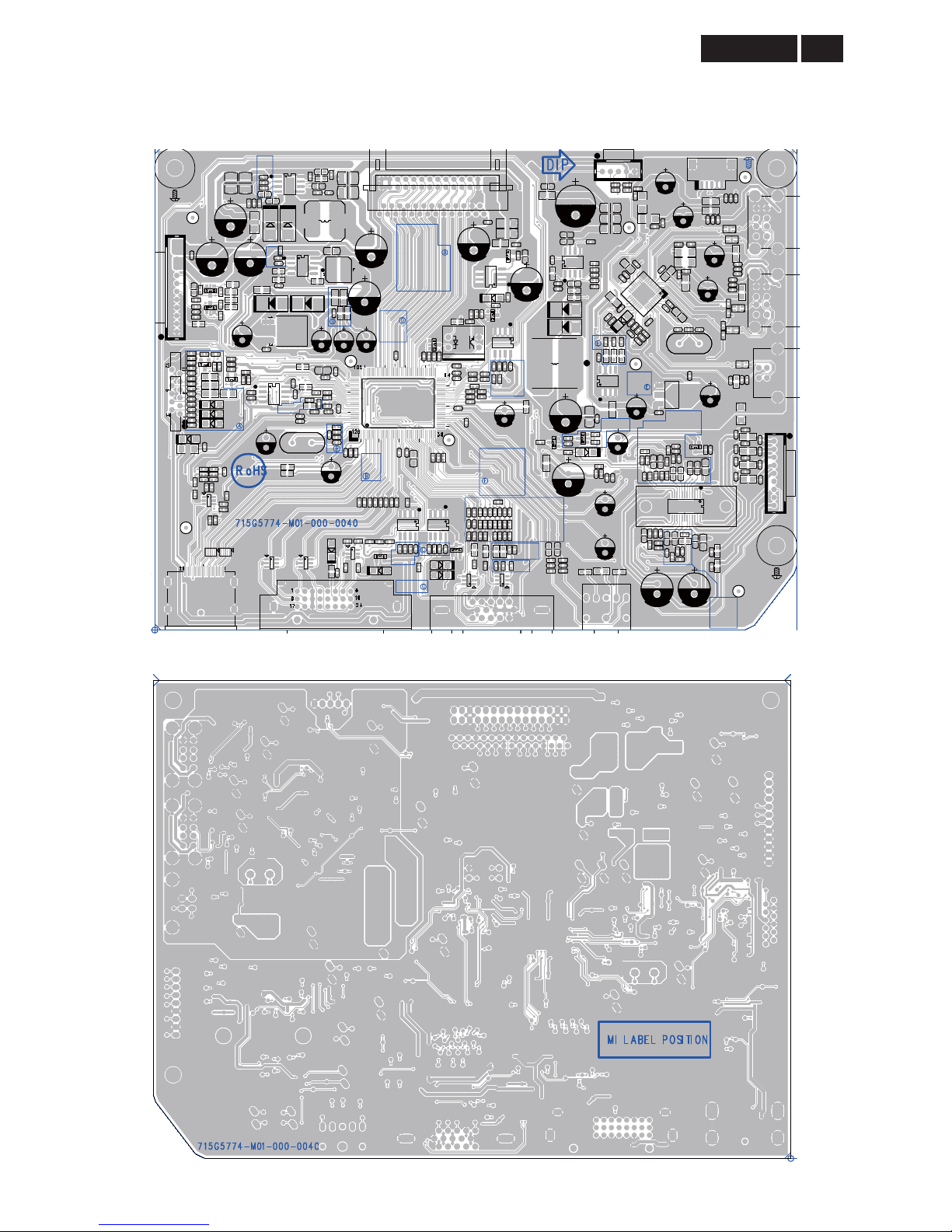
39
Meridian 3
7. PCB Layout
7.1 Scaler Board (715G5774M01000004K)
Remark: Parts position can be searched by using FIND function in PDF.
CN601
D101
D102
D601
FB101
FB102
FB103
Q401
Q402
Q602
Q603
Q701
Q702
Q466
U102
U106 U107
U108
U109
U110
U403
ZD101
ZD102
ZD103
ZD104
ZD105
U402
C715
F101
U104
U105
U101
U103
D702
CN602
CN403
CN401
C603
C604
C709
C710
C712
C718
C721
C722
C725
C711
C614
C615
C440
C729
C719
C610
C716
C720
R466
R480
R481
R612
R613
R619
R701
R702
R708
R712
R718
R721
R723
R724
R735
FB104
FB401
FB402
FB405
FB406
FB407
FB408
FB409
FB703
R473
R474
R475
FB403
FB404
FB602
FB603
FB604
FB605
FB606
FB702
FB704
D701
Q704
U701
U703
D703D704
D705
Q601
Q706
U702
D504
ZD401
ZD402
ZD403
CN402
CN501
L501
L502
L503
L504
L505
L506
C501
C506
C507
C508
C617
C618
C619
C622
C623
C624
C626
C546
C548
C549
C616
C627
C503
C504
C505
C513
FB507
FB501
FB502
FB503
FB504
FB505
FB506
FB508
FB509
FB601
L702
R501
R502
R515
R527
R529
R531
R621
R631
F501
F502
F503
F504
FB701
D501
D502
U503
U501
U504
Q705
N701
SET7
SET2
SET3
SET1
C436
C730
C701
R139
L701
R443
R101
R102
R103
R104
R105R106
R107
R108
R109
R110
R111
R112
R113
R114
R115
R116
R117
R118
R119
R120
R121
R122
R123
R124
R125
R126
R127
R128
R129
R130
R131
R132
R133
R134
R135
R136
R137
R138
R140
R141
R150
R151R152
R153
R154
R156
R157R158
R159
R161
R162
R163
R164
R165
R401
R402
R403
R404
R405
R408
R409
R410
R411
R412
R413
R414
R416
R417
R418
R419
R420
R421
R422
R424
R426
R427
R428
R429
R430
R431
R432
R433
R435
R436
R438
R439
R440
R441
R442
R446
R447
R448
R449
R450
R451
R452
R453
R456
R457
R458
R460R461
R462
R463
R464
R465
R467
R468
R469
R470
R471
R472
R601
R602
R603
R604
R605
R606
R607
R608
R609
R610
R611
R614
R618
R622
R704
R705
R707
R710
R711
R714
R719
R720
R722
R168
R727
R730
R166
R167
R486
R731
R444
R445
R706
R406
R407
R415
R423
R425
R434
R437
R490
R503
R504
R505
R506
R507
R508
R509
R510
R511
R512
R513
R514
R516 R517
R518 R519
R520
R521
R522
R523
R524
R525
R526
R528
R530
R532
R616
R617
R620
R623R624
R625
R626
R627
R628
R629
R630
R632
R633
R634
R635
R636
R640
R641
R709
R713
R715
R716
R717
R726
R728
R729
R482
C102
C103
C104
C105
C106
C107
C108
C109
C110
C111
C114
C115
C116
C117
C118
C120
C122
C401
C404
C405
C406
C407
C409
C410
C411
C412
C414
C416
C419
C420
C421
C425
C426
C427
C428
C430
C431
C432
C433
C434
C435
C437
C438
C439
C441
C442
C509
C510
C511
C512
C515
C517
C519
C521
C523
C525
C526
C528
C529
C530
C531
C532
C533
C534
C535
C536
C537
C538
C539
C540
C541
C542
C543C544
C545
C547
C550
C551
C552
C553
C554
C555
C586
C602
C605
C606
C607
C608
C609
C611
C613
C625
C628
C629 C630C631
C632
C633 C634C635
C702
C705
C707
C708
C713
C714
C717
C723
C724
C726
C728
CN102
CN103
X401
X501
CN407
CN408
CN503
CN502
SET4
SET21
SET9
SET15
SET14
SET16
SET6
SET8
CN504
R703
U601
C514
C443
R455
OC401
C502
U401
CN101
U502
C621
C601
C703
C620
C727
C423
C418
C704
C417
C408
C424
C403
C422
C516
C518
C520
C522
C524
C527
C612
C706
Remark: Parts position can be searched by using FIND function in PDF.

!
40
Meridian 3
Scaler Board (715G5774M1A000004S) (Only for 240P4QPYE)
Remark: Parts position can be searched by using FIND function in PDF.
CN601
D101
D102
D601
FB101
FB102
FB103
Q401
Q402
Q602
Q603
Q701
Q702
Q466
U102
U106 U107
U108
U109
U110
U403
ZD101
ZD102
ZD103
ZD104
ZD105
U402
C715
F101
U104
U105
U101
U103
D702
CN602
CN403
CN401
C603
C604
C709
C712
C718
C721
C725
C711
C614
C615
C440
C729
C719
C610
C716
C720
R466
R480
R481
R612
R613
R619
R701
R702
R708
R712
R718
R721
R723
R724
R735
FB104
FB401
FB402
FB405
FB406
FB407
FB408
FB409
FB703
R473
R474
R475
FB403
FB404
FB602
FB603
FB604
FB605
FB606
FB702
FB704
D701
Q704
U701
U703
D703D704
D705
Q601
Q706
U702
D504
ZD401
ZD402
ZD403
CN402
CN501
L501
L502
L503
L504
L505
L506
C501
C506
C507
C508
C617
C618
C619
C622
C623
C624
C626
C546
C548
C549
C616
C627
C503
C504
C505
C513
FB507
FB501
FB502
FB503
FB504
FB505
FB506
FB508
FB509
FB601
L702
R501
R502
R515
R527
R529
R531
R621
R631
F501
F502
F503
F504
FB701
D501
D502
U503
U501
U504
Q705
CN701
SET7
SET2
SET3
SET1
R139
L701
R443
R101 R102
R103
R104
R105R106
R107
R108
R109
R110
R111
R112
R113
R114
R115
R116
R117
R118
R119
R120
R121
R122
R123
R124
R125
R126
R127
R128
R129
R130
R131
R132
R133
R134
R135
R136
R137
R138
R140
R141
R150
R151R152
R153
R154
R156
R157R158
R159
R161
R162
R163
R164
R165
R401
R402
R403
R404
R405
R408
R409
R410
R411
R412
R413
R414
R416
R417
R418
R419
R420
R421
R422
R424
R426
R427
R428
R429
R430
R431
R432
R433
R435
R436
R438
R439
R440
R441
R442
R446
R447
R448
R449
R450
R451
R452
R453
R456
R457
R458
R460R461
R462
R463
R464
R465
R467
R468
R469
R470
R471
R472
R601
R602
R603
R604
R605
R606
R607
R608
R609
R610
R611
R614
R618
R622
R704
R705
R707
R710
R711
R714
R719
R720
R722
R168
R727
R730
R166
R167
R486
R731
R444
R445
R706
R406
R407
R415
R423
R425
R434
R437
R490
R503
R504
R505
R506
R507
R508
R509
R510
R511
R512
R513
R514
R516 R517
R518 R519
R520
R521
R522
R523
R524
R525
R526
R528
R530
R532
R616
R617
R620
R623R624
R625
R626
R627
R628
R629
R630
R632
R633
R634
R635
R636
R640
R641
R709
R713
R715
R716
R717
R726
R728
R729
R482
C102
C103
C104
C105
C106
C107
C108
C109
C110
C111
C114
C115
C116
C117
C118
C120
C122
C401
C404
C405
C406
C407
C409
C410
C411
C412
C414
C416
C419
C420
C421
C425
C426
C427
C428
C430
C431
C432
C433
C434
C435
C437
C438
C439
C441
C442
C509
C510
C511
C512
C515
C517
C519
C521
C523
C525
C526
C528
C529
C530
C531
C532
C533
C534
C535
C536
C537
C538
C539
C540
C541
C542
C543C544
C545
C547
C550
C551
C552
C553
C554
C555
C586
C602
C605
C606
C607
C608
C609
C611
C613
C625
C628
C629 C630
C631
C632 C633 C634C635
C702
C705
C707
C708
C713
C714
C717
C723
C724
C726
C728
CN102
CN103
X401
X501
CN407
CN408
CN503
CN502
SET4
SET21
SET9
SET15
SET14
SET16
SET6
SET8
CN504
R703
C443
R455
OC401
C502
CN101
U502
C621
C601
C703
C620
C727
C514
C422
C423
C418
C704
C417
C408
C424
C403
C516
C518
C520
C522
C524
C527
C612
C706
C436
C701
C710
C722
C730
U401
U601
Remark: Parts position can be searched by using FIND function in PDF.

41
Meridian 3
7.2 Power Board (715G5164P02002001M)
Remark: Parts position can be searched by using FIND function in PDF.
J4
J14 J15
C1
R1
C2
CN905
D902
D903
D906
FB601
FB801
FB802
FB902
IC902
L801
L901
L904
Q901
R919
R946R947
ZD902
J904
D905
C601
C603
HS3
HS2
HS1
J902
J905
J908
J918
J913
J907
FB901
J804
J901
J906
J916
J914
J915
J917
J803
J801
J802
J920
J919
J921
R917
J910
J16
J911
J912
BD901
C903
CN903
NR901
CN902
MH4
C906
D904
ZD802
C915
C917
C918
CN801
CN802
CN602
CN803
FB803
D907
C900
C901
C902
C804
C803
L902
J922
C619
C620
C913
C920
J924
J923
FB804
MH1
CN901
FB903
GND2
GND1
C907
C905
C905A
J925
J903
C916
L903
L905
F901
F903
Q903
IC903
C813
F902
CN603
T901
CN601
Remark: Parts position can be searched by using FIND function in PDF.
J1
J3
J44
J45
C614
C608
C609
C615
C605
C801
C805
C806
C807
C811
C814
C815
C820C821
C910
C911
C912
C914
C919
C922
C924
C929
C930
C931
C932
C933
C934
C935
IC801
IC901
R632
R631
R609
R610
R626
R606
R602
R611
R601
R618
R607
R620
R619
R627
R628
R801
R802
R804
R805
R806
R807
R808
R809
R810
R812
R813
R814
R822
R824
R842
R844
R845
R846
R847
R848
R849
R850
R852
R901
R902
R905
R908
R910
R912
R916
R918
R920
R923
R924
R925
R932
R935
R939
R943
R961
R962
C613
C606
C607
C602
C618
C625
R624
C610
C611
C612
C616
C617
C622
C630
C631
C623
C624
R605
R612
R621
R625
FB602
FB603
FB604
FB605
FB606
R633
U601
JR901
JR903
JR905
JR906
R907
R913R914
R906
JR801
JR902
JR904
R911
R851
Q801
J5
J6
J7
J8
R927
R933
R940
R930
R903
R926
C812
Q604
Q601
Q603
R603
R604
C621
JR802
R815
C921
JR907
R941
R936

!
42
Meridian 3
7.3 Key Board (715G5446K01000004S)
Remark: Parts position can be searched by using FIND function in PDF.
TP5
TP1
TP2
TP3
TP4
CN2
CN11
CN1
Remark: Parts position can be searched by using FIND function in PDF.
TP6
TP7
C001
C002
C003
C004
C005
R004
R005
U001
ZD001
ZD002
CN10
CN001
Key Board (715G6073K01000004S) (Only for 240P4QPYE)
Remark: Parts position can be searched by using FIND function in PDF.
TP5
TP1
TP2
TP3
TP4
CN2 CN1
Remark: Parts position can be searched by using FIND function in PDF.
TP6
TP7
C001
C002
C003
C004
C005
R004
R005
U001
ZD001
ZD002
CN001
7.4 IR Board (715G5459R01000004S)
Remark: Parts position can be searched by using FIND function in PDF.
ZD3
R1
R3
R12R15
ZD1ZD2
C311
C312
C313
C314
C315
C316
C317
C318
C319
C320
Q311
Q312
Q313
R311
R312
R313
R314
R315
R316
R317
R318
R319
R320
R321
R322
R323
R324
U311
U313
ZD311
ZD312
ZD313
LED312
U312
LED311
Remark: Parts position can be searched by using FIND function in PDF.
R2
R4
R13 R16
CN311 CN312
7.5 Head Phone Jack Board (715G5462T01000004Q) (Only for 240P4QPYE)
Remark: Parts position can be searched by using FIND function in PDF.
CN1
CN2
CN681
CN683
CN684
CN3
CN4
U681
U682
Remark: Parts position can be searched by using FIND function in PDF.

43
Meridian 3
8. Wring Diagram
240P4QPYN
CN103
Panel
Scaler Board
12
12
1
CN408
30
1
CN701
U
S
B
1
CN402
CN102
CN101
CN502
CN503
CN504
DP
DVI
D-SUB
Power Board
CN802
1
6
11
1
CN903
CN901
CN905
Key Board
CN001
1
6
IR Board
CN311
1
6
CN312
112

!
44
Meridian 3
240P4QPYE
CN103
Panel
Scaler Board
12
12
1
CN408
30
1
CN701
U
S
B
1
CN402
CN102
CN101
CN502
CN503
CN504
DP
DVI
D-SUB
Power Board
CN802
1
6
11
1
CN903
CN901
CN905
Key Board
CN001
IR Board
CN311
CN312
1
1
12
HEAD PHONE JACK
CN681
CN683
CN684
SPK
SPK
1
1
4
1
9
CN602
9
1
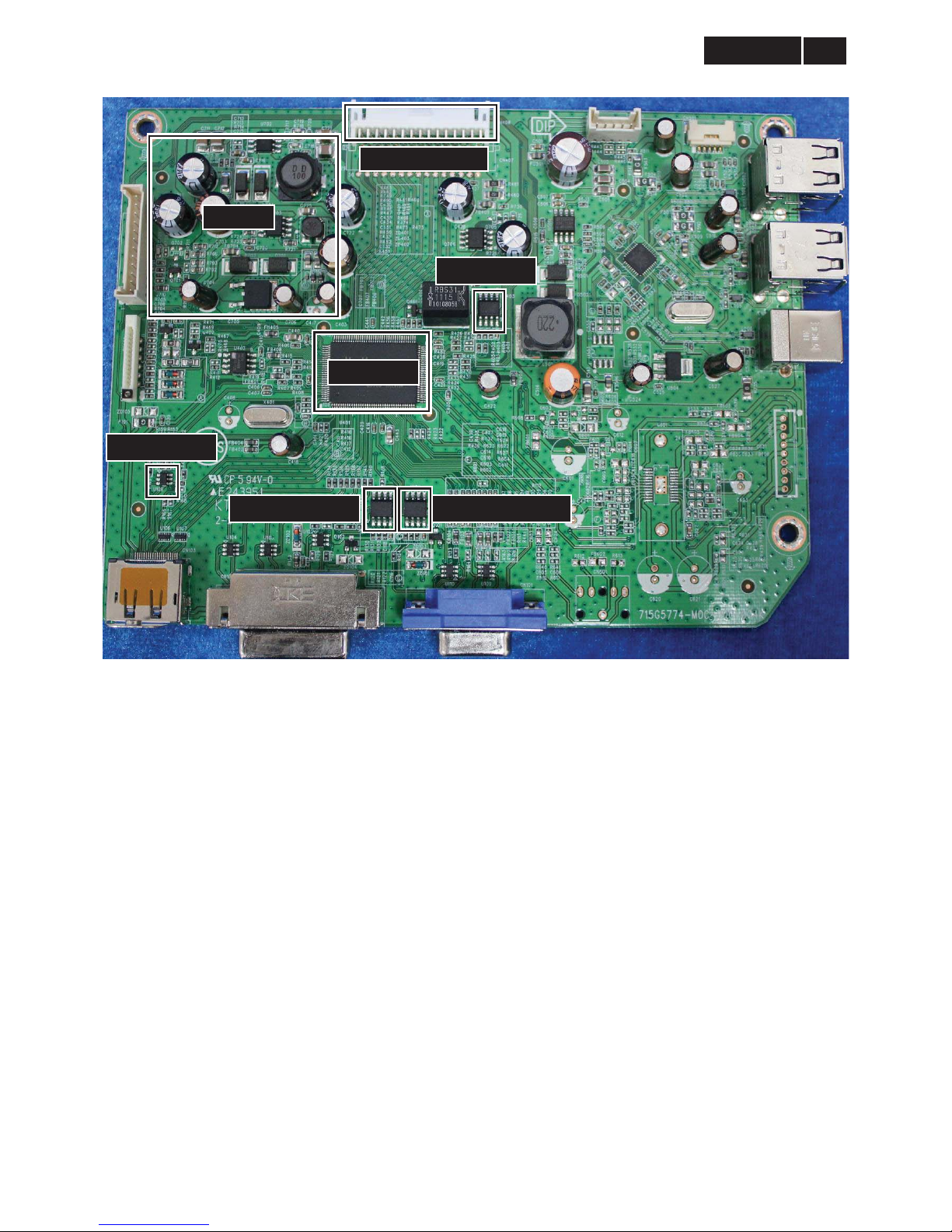
45
Meridian 3
9. Scaler Board Overview
DC-DC
FFC Cable
Scaler IC
Flash ROM
D-SUB EEPROM
DP EEPROM
DVI EEPROM

!
46
Meridian 3
10. Mechanical Instructions
Step 1: Remove the stand-base ASSY
1. Push the button and remove the stand-base ASSY.
Step 2: Separate the bezel and the rear cover,
and remove the boards.
1. Remove the screws and use disassembly tool to
open all the latches along the edge of the Rear
Cover
2. Disconnect all the connectors and remove the
screws to separate the shield and boards.
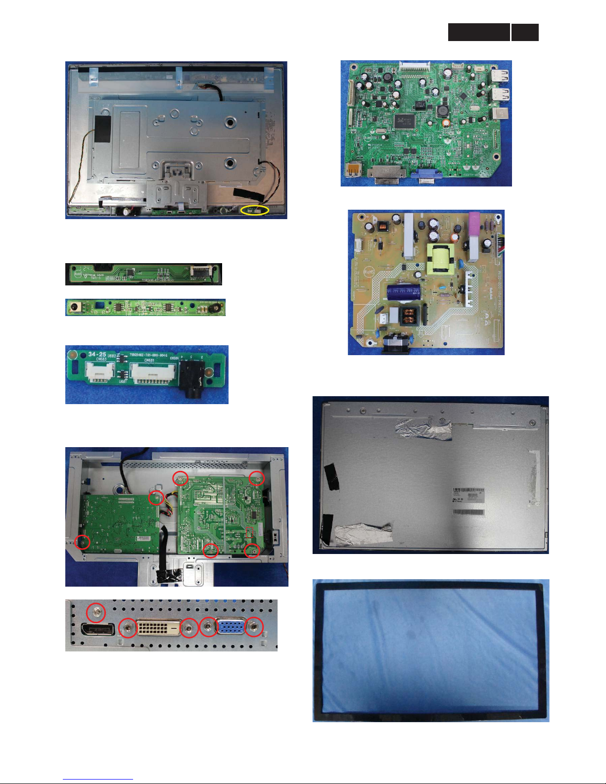
47
Meridian 3
(Only for 240P4QPYE)
3. The key board, the IR board and the head phone
jack board.
(Only for 240P4QYE):
4. Remove the screws and connector to remove the
scaler board and the power board.
The scaler board.
The power board.
Step 3:The panel and the bezel.
1. The panel
2. The Bezel.

!
48
Meridian 3
11. Repair Flow Chart
1. No Power
OK
NG
No power
Check power cable is
tightened?
Check Power “On/Off”
is “On”?
Re-plug the power cable
Replace main board and check connections
Check the LED
indicator is OK?
Check the AC power
Replace the power board and check connections
OK
NG
OK
NG
NG
Turn on the Power “On/Off” switch
Replace key board and check connections
NG

49
Meridian 3
2.
Video (Power LED White)
No Video (Power LED White)
Press the power
button is OK?
Check the FFC cable
or panel
The end
NG
OK
OK
NG
Replace the main board
Replace the power
board and connection
Replace the FFC cable
or panel
NG
The end
Replace the key board
NG
OK
Replace the main
board and connection
OK

!
50
Meridian 3
3. DIM
OK
The end
OK
The end
OK
The end
DIM (image overlap, focus or flicker)
Reset in factory mode
Set to the optimal
frequency, select the
recommended fre
q
uenc
y
Pull out signal cable and
check “Self Test Feature
Check” is ok?
Check the signal cable
and the PC
Readjust the phase and pixel
clock in the user mode
Replace the main board
Replace the panel
NG
NG
NG
OK
NG
NG
OK
The end
OK
NG

51
Meridian 3
4. Color is not optimal
NG
Color is not optimal
Miss color
Color shift
Replace the signal cable
Pull out the signal cable
and check the screen
color display is normal?
The end
Replace the signal cable or PC
Reset the factory mode
In the user mode, set the “color
settings” until customer satisfy
Replace the main board
NG
OK
NG
OK
NG

!
52
Meridian 3
12. ISP Instruction
When do the parts, need the tools as follow:
ISP JIG: 715GT089-B/C VGA cable
TPV P/N: 089G728 GAA DB
PC Monitor USB cable
TPV P/N: 089G1758 X
USB port driver ISP tool: New F/W
Installation patch

53
Meridian 3
12.1. Connect the ISP board, PC and monitor as follow:
12.2 Install the USB driver.
1. When insert the USB cable to PC USB port, will pop up a Hardware Wizard to help you install the USB driver if
you use this ISP board first time. You can install it successfully as the below instruction step by step.
Remark: The USB driver files path: D:\FTC100103(Mstar)\FTCUSB.INF

!
54
Meridian 3
4. Install RTD tool.
After installation the USB serial port driver, please check the port. Look the properties of “my Computer”

55
Meridian 3
12.3 Install the RTD tool.
1. Click to install it. After installation, double- clicks the icon to run it.
炷Note: Must to install patch firstly, and Click RTD Customer Tool V2.1.exe to installed in windows XP. RTD
Customer Tool V2.1.exe can be installed in Windows 7 directly.炸
2. Choose the USB communication way.

!
56
Meridian 3
3. Click “ISP” and “ISP Option” to set the parameter.
4. Set the Basic Setting.

57
Meridian 3
5. Set the flash Protect to disable flash device protect when programming.
6. Do erase setting as below.

!
58
Meridian 3
7. Close the “ISP Option” window and click the “BigBin” to load the correct F/W.
8. Click to start programming.

59
Meridian 3
9. After about 2minutes, there will pop up message as below figure which promotes the upgrade successful.

!
60
Meridian 3
12.4. Check the FW version after upgrade.
1. The way to open factory menu.
(1)Connect video source to monitor and AC on.
(2)The way to factory menu: Press “MENU” and “+” keys synchronously (The rightmost and leftmost keys in the
touch keyboard), and DC on. When the screen lights, release the two keys and press “MENU” again to open
factory menu.
“+” key “menu” key DC key
(3)Select “factory” and press menu key to open factory menu as below.
(4)Please do “Auto Color” in factory menu after change main board and upgrade F/W.
Check this
F/W version.

61
Meridian 3
2. Do factory reset in user menu. User menu – Setup – Reset - Yes.
(1) Restart the monitor after open factory menu. And then open the user menu.
(2) Factory reset will turn off “Burn in” mode which screen color switches amon g red, green, blue and black.

!
62
Meridian 3
13. DDC Instruction
General
DDC Data Re-programming
In case the main EEPROM with Software DDC which store all factory settings were replaced because a defect
repaired monitor’ the serial numbers have to be re-programmed.
It is advised to re- soldered the main EEPROM with Software DDC from the old board onto the new board if circuit
board have been replaced, in this case the DDC data does not need to be re-pro grammed.
Additional information about DDC (Display Data Channel) may be obtained from Video Electronics Standards
Association (VESA). Extended Display Identification Data (EDID) information may be also obtained from VESA.
LPT cable (male to male) VGA cable 12V DC adapter
TPV P/N: N/A TPV P/N: 089G728 GAA DB TPV P/N: ADPC12416BEP
ISP JIG: 715GT034-B PC Monitor
LPT port driver ISP tool: VgaSinglePort.exe EDID

63
Meridian 3
13.1 Connect the ISP board, PC and monitor as follow:
13.2 Install LPT drive
1. Double click the icon to install the driver.
2. Restart PC after installation.
13.3 Prepare the EDID written
1. Change the EDID files name as below rule.
Anolog EDID WA.dat Digital EDID WD.dat
Displayport EDID WP.dat
2. Copy these four files to one folder named as philips 240P4QPY which must contains “config.ini” file.
3. Copy philips 240P4QPY to DDC folder and put DDC and ISP tool together.

!
64
Meridian 3
13.4. Run the ISP tool.
1. Double-click the icon to open the tool.
2.(1) Tick the “Analog+DVI” and cli ck “Loadfile” to set the parameters.
(2) Manufacturer: PHL Product Code: 08CA Model Name: Philips 240P4
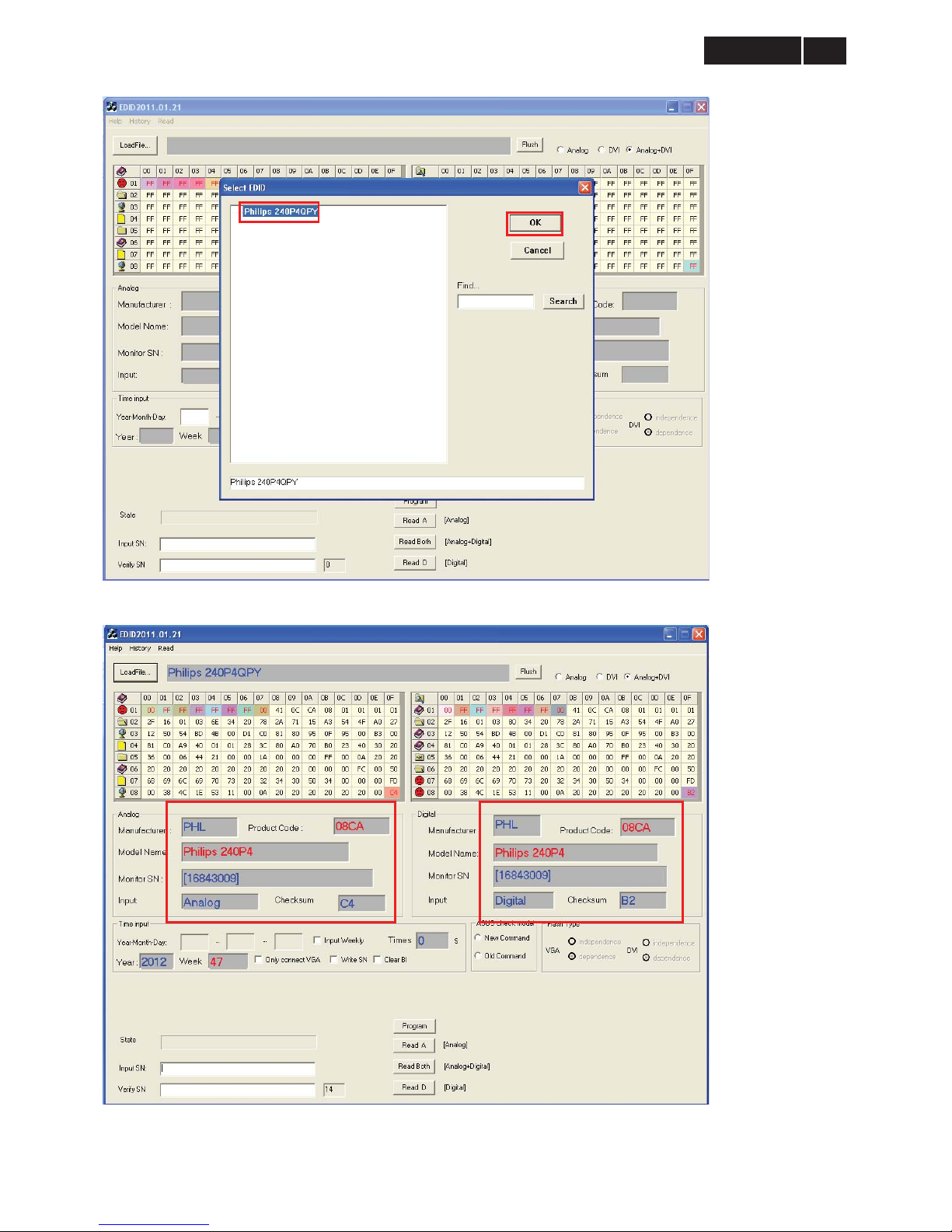
65
Meridian 3
3. Select the EDID folder. Select Philips 240P4QPY
4. Load EDID successful. In the EDID tool, you can know the EDID information.

!
66
Meridian 3
5. Tick the “Only connect VGA” and “Write SN”, and type in the 14 digit S/N.
Remark: Please turn on the monitor before click “Program”. Or else you maybe write EDID fail.
6. Start writing. Click “Program” to start writing. When the green “PASS” appear, the process is finished.

67
Meridian 3
7. Check the S/N in monitor user menu.
Press “MENU” and select “Setup/ information”,you can check the SN in the botton of menu interface.
13.5. Troubleshooting.
1. Can’t write error.
2. Try below few ways to cure can’t write errors!
(1)
AC on the monitor and turn on it.(Restart the monitor)
(2)Take apart the monitor and connect the 7pin of EEPROM to GND to diable write protection then write EDID
one by one.
(3)Set the Burn in on last to try again.

!
68
Meridian 3
240P4QPYNS/00 EDID
Analog
00 01 02 03 04 05 06 07 08 09 0A 0B 0C 0D 0E 0F
-----------------------------------------------
00| 00 FF FF FF FF FF FF 00 41 0C CA 08 01 01 01 01
10| 2F 16 01 03 6E 34 20 78 2A 71 15 A3 54 4F A0 27
20| 12 50 54 BD 4B 00 D1 C0 81 80 95 0F 95 00 B3 00
30| 81 C0 A9 40 01 01 28 3C 80 A0 70 B0 23 40 30 20
40| 36 00 06 44 21 00 00 1A 00 00 00 FF 00 0A 20 20
50| 20 20 20 20 20 20 20 20 20 20 00 00 00 FC 00 50
60| 68 69 6C 69 70 73 20 32 34 30 50 34 00 00 00 FD
70| 00 38 4C 1E 53 11 00 0A 20 20 20 20 20 20 00 C4
EDID Structure Version/Revision: 01 03
<-Vendor/Pro duct Identification:->
ID Manufacturer Name: PHL
ID Product Code: 08CA
ID Serial Number: No Use
Week of Manufacture: 47
Year of Manufacture: 2012
<-Basic Display Parameters/Features:->
Video i/p definition: Analog
Max. H. Image Size : 52cm
Max. V. Image Size : 32cm
Display Gamma : 2.2
<-Color Characteristics:->
Rx: 0.638 Gx: 0.309 Bx: 0.152 Wx: 0.313
Ry: 0.331 Gy: 0.626 By: 0.071 Wy: 0.329
<-Established T imings:->
Established Timings 1:BD
720 x 400 @ 70Hz VGA,IBM
640 x 480 @ 60Hz VGA,IBM
640 x 480 @ 67Hz Apple,Mac II
640 x 480 @ 72Hz VESA

69
Meridian 3
640 x 480 @ 75Hz VESA
800 x 600 @ 60Hz VESA
Established Timings 2:4B
800 x 600 @ 75Hz VESA
1024 x 768 @ 60Hz VESA
1024 x 768 @ 75Hz VESA
1280 x1024 @ 75Hz VESA
Established Timings 3:00
<-Standa rd T i ming Identification:->
1920 x 1080 @ 60Hz
1280 x 1024 @ 60Hz
1440 x 900 @ 75Hz
1440 x 900 @ 60Hz
1680 x 1050 @ 60Hz
1280 x 720 @ 60Hz
1600 x 1200 @ 60Hz
<-Detailed Timing Descriptions:->
FC (Monitor Name) : Philips 240P4
FD (Monitor Limits):
Min. V. rate: 56 Hz
Max. V. rate: 76 Hz
Min. H. rate: 30 KHz
Max. H. rate: 83 KHz
Max. P Clock: 170 MHz
FF (Monitor SN) :
Detailed Timing : 1920x1200 @ 60Hz
Extension Flag : 00
Block0 Checksum : C4

!
70
Meridian 3
Digital
00 01 02 03 04 05 06 07 08 09 0A 0B 0C 0D 0E 0F
-----------------------------------------------
00| 00 FF FF FF FF FF FF 00 41 0C CA 08 01 01 01 01
10| 2F 16 01 03 80 34 20 78 2A 71 15 A3 54 4F A0 27
20| 12 50 54 BD 4B 00 D1 C0 81 80 95 0F 95 00 B3 00
30| 81 C0 A9 40 01 01 28 3C 80 A0 70 B0 23 40 30 20
40| 36 00 06 44 21 00 00 1A 00 00 00 FF 00 0A 20 20
50| 20 20 20 20 20 20 20 20 20 20 00 00 00 FC 00 50
60| 68 69 6C 69 70 73 20 32 34 30 50 34 00 00 00 FD
70| 00 38 4C 1E 53 11 00 0A 20 20 20 20 20 20 00 B2
EDID Structure Version/Revision: 01 03
<-Vendor/Pro duct Identification:->
ID Manufacturer Name: PHL
ID Product Code: 08CA
ID Serial Number: No Use
Week of Manufacture: 47
Year of Manufacture: 2012
<-Basic Display Parameters/Features:->
Video i/p definition: Digital
Max. H. Image Size : 52cm
Max. V. Image Size : 32cm
Display Gamma : 2.2
<-Color Characteristics:->
Rx: 0.638 Gx: 0.309 Bx: 0.152 Wx: 0.313
Ry: 0.331 Gy: 0.626 By: 0.071 Wy: 0.329
<-Established T imings:->
Established Timings 1:BD
720 x 400 @ 70Hz VGA,IBM
640 x 480 @ 60Hz VGA,IBM
640 x 480 @ 67Hz Apple,Mac II
640 x 480 @ 72Hz VESA
640 x 480 @ 75Hz VESA

71
Meridian 3
800 x 600 @ 60Hz VESA
Established Timings 2:4B
800 x 600 @ 75Hz VESA
1024 x 768 @ 60Hz VESA
1024 x 768 @ 75Hz VESA
1280 x1024 @ 75Hz VESA
Established Timings 3:00
<-Standa rd T i ming Identification:->
1920 x 1080 @ 60Hz
1280 x 1024 @ 60Hz
1440 x 900 @ 75Hz
1440 x 900 @ 60Hz
1680 x 1050 @ 60Hz
1280 x 720 @ 60Hz
1600 x 1200 @ 60Hz
<-Detailed Timing Descriptions:->
FC (Monitor Name) : Philips 240P4
FD (Monitor Limits):
Min. V. rate: 56 Hz
Max. V. rate: 76 Hz
Min. H. rate: 30 KHz
Max. H. rate: 83 KHz
Max. P Clock: 170 MHz
FF (Monitor SN) :
Detailed Timing : 1920x1200 @ 60Hz
Extension Flag : 00
Block0 Checksum : B2

!
72
Meridian 3
Display Port
00 01 02 03 04 05 06 07 08 09 0A 0B 0C 0D 0E 0F
--------------------Block 0--------------------
00| 00 FF FF FF FF FF FF 00 41 0C CA 08 00 00 00 00
10| 2F 16 01 04 A5 34 20 78 3A 71 15 A3 54 4F A0 27
20| 12 50 54 BD 4B 00 D1 C0 81 80 95 0F 95 00 B3 00
30| 81 C0 A9 40 01 01 28 3C 80 A0 70 B0 23 40 30 20
40| 36 00 06 44 21 00 00 1A 00 00 00 FF 00 0A 20 20
50| 20 20 20 20 20 20 20 20 20 20 00 00 00 FC 00 50
60| 68 69 6C 69 70 73 20 32 34 30 50 34 00 00 00 FD
70| 00 38 4C 1E 53 11 00 0A 20 20 20 20 20 20 01 7F
--------------------Block 1--------------------
00| 02 03 10 B1 4B 01 02 03 04 05 90 11 12 13 14 1F
10| 02 3A 80 18 71 38 2D 40 58 2C 45 00 06 44 21 00
20| 00 1E 8C 0A D0 8A 20 E0 2D 10 10 3E 96 00 06 44
30| 21 00 00 18 01 1D 00 72 51 D0 1E 20 6E 28 55 00
40| 06 44 21 00 00 1E 8C 0A D0 90 20 40 31 20 0C 40
50| 55 00 06 44 21 00 00 18 00 00 00 00 00 00 00 00
60| 00 00 00 00 00 00 00 00 00 00 00 00 00 00 00 00
70| 00 00 00 00 00 00 00 00 00 00 00 00 00 00 00 E9
-------------------------------------------------------
Block 0:
EDID Structure Version/Revision: 01 04
<-Vendor/Pro duct Identification:->
ID Manufacturer Name: PHL
ID Product Code: 08CA
ID Serial Number: 0
Week of Manufacture: 47
Year of Manufacture: 2012
<-Basic Display Parameters/Features:->
Video i/p definition: Digital
Max. H. Image Size : 52cm
Max. V. Image Size : 32cm
Display Gamma : 2.2
<-Color Characteristics:->
Rx: 0.638 Gx: 0.309 Bx: 0.152 Wx: 0.313
Ry: 0.331 Gy: 0.626 By: 0.071 Wy: 0.329

73
Meridian 3
<-Established T imings:->
Established Timings 1:BD
720 x 400 @ 70Hz VGA,IBM
640 x 480 @ 60Hz VGA,IBM
640 x 480 @ 67Hz Apple,Mac II
640 x 480 @ 72Hz VESA
640 x 480 @ 75Hz VESA
800 x 600 @ 60Hz VESA
Established Timings 2:4B
800 x 600 @ 75Hz VESA
1024 x 768 @ 60Hz VESA
1024 x 768 @ 75Hz VESA
1280 x1024 @ 75Hz VESA
Established Timings 3:00
<-Standa rd T i ming Identification:->
1920 x 1080 @ 60Hz
1280 x 1024 @ 60Hz
1440 x 900 @ 75Hz
1440 x 900 @ 60Hz
1680 x 1050 @ 60Hz
1280 x 720 @ 60Hz
1600 x 1200 @ 60Hz
<-Detailed Timing Descriptions:->
Detailed Timing : 1920x1200 @ 60Hz
FF (Monitor SN) :
FC (Monitor Name) : Philips 240P4
FD (Monitor Limits):
Min. V. rate: 56 Hz
Max. V. rate: 76 Hz
Min. H. rate: 30 KHz
Max. H. rate: 83 KHz
Max. P Clock: 170 MHz
Extension Flag : 01

!
74
Meridian 3
Block0 Checksum : 7F
-------------------------------------------------------
Block 1:
Extended Block Type: CEA 861B
Detailed Timing Blocks start at Byte: 10
DTV Underscan YES
DTV Basic Audio NO
YCbCr (4:4:4) YES
YCbCr (4:2:2) YES
<-Video Short Block Description:->
640 x 480 P 59.94/60Hz 4:3
720 x 480 P 59.94/60Hz 4:3
720 x 480 P 59.94/60Hz 16:9
1280 x 720 P 59.94/60Hz 16:9
1920 x 1080 I 59.94/60Hz 16:9
1920 x 1080 P 59.94/60Hz 16:9
720 x 576 P 50Hz 4:3
720 x 576 P 50Hz 16:9
1280 x 720 P 50Hz 16:9
1920 x 1080 I 50Hz 16:9
1920 x 1080 P 50Hz 16:9
<-Speaker Allocation:->
<-Detailed Timing Descriptions: ->
Detailed Timing Descriptions: 1920x1080 @ 60Hz
H Image Size: 518 mm V Image Size: 324 mm
Pixel Clock: 148 Hz Refreshed Mode: Non-Interlaced
Detailed Timing Descriptions: 720x480 @ 60Hz
H Image Size: 518 mm V Image Size: 324 mm
Pixel Clock: 27 Hz Refreshed Mode: Non-Interlaced
Detailed Timing Descriptions: 1280x720 @ 60Hz
H Image Size: 518 mm V Image Size: 324 mm
Pixel Clock: 74 Hz Refreshed Mode: Non-Interlaced

75
Meridian 3
Detailed Timing Descriptions: 720x576 @ 50Hz
H Image Size: 518 mm V Image Size: 324 mm
Pixel Clock: 27 Hz Refreshed Mode: Non-Interlaced
Block1 Checksum : E9
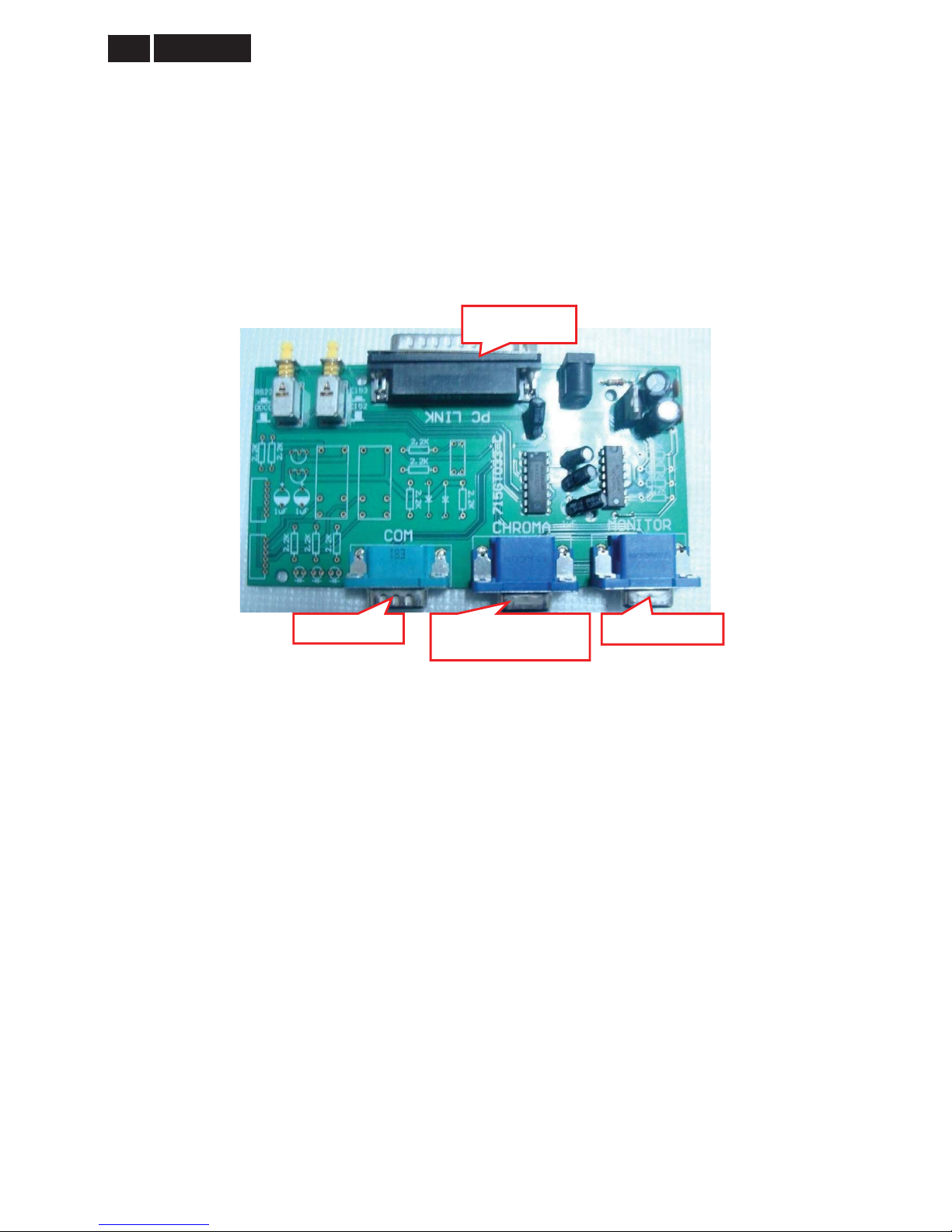
!
76
Meridian 3
14. White Balance, Luminance Adjustment
1. Apparatuses and program: analyzer CA-210, PC, tool, FGA adjustment program (Philips LEDFGA.DDCI),
Pattern generator.
2. Equipment installation:
a. Connect analyzer CA-210 to PC by USB connector, inst all drive p rogram CA-SDK Ver4.00 for CA-210 and restart
PC after finish installing
b. Install Port95NT drive program, set PC printer connector mode as ECP mode and reset PC after finish installing.
c. Connect tool as follow:
Note: It’s not necessary to connect Port2.
3. Adjustment
Preparation before adjustment:
a. Monitor should be warmed up for more than half an hour .
b. Make sure that the tools are connected right and drive programs have been installed OK.
4. Adjustment process:
a. Press the power of CA-210, shut off the lens, press 0-Cal and open the lens after analyzer reset.
b. Open white balance adjustment program, select the right parameter according with the program and click OK.
c. Make sure that the lens of CA-210 aims at the center of the screen, then click START to adjust.
d. After finish adjusting, the adjustment program displays pass, and the START button changes for NEXT, which
means that you can adjust another monitor.
To PC LPT
To BSG-265A or
e
q
uivalent instrument
To PC Port 2
Philips model

77
Meridian 3
5. Color Temp confirmation
Connect the signal to the monitor, the monitor displays white-picture, use CA-210 to measure the Color Temp of the
screen center and select the OSD to make sure whether the Color Temps accord with the SPEC.
CIE
coordinates
11500K 9300K 8200K 7500K 6500K/sRGB sRGB 5000K
x 0.270±0.02 0.283±0.02 0.291±0.02 0.298±0.02 0.313±0.02 0.313±0.02 0.345±0.02
y 0.281±0.02 0.297±0.02 0.306±0.02 0.314±0.02 0.329±0.02 0.329±0.02 0.357±0.02
6. How to enter into the factory mode:
1. Connect the video source and power off the monitor.
2. Press and buttons at the same time, power on the monitor, and then press the menu again; the
picture will appear on the top left corner.
3. Select the “Factory” and press the “MENU” button to enter the factory mode.

!
78
Meridian 3
15. Monitor Exploded View
240P4QPYN

79
Meridian 2
240P4QPYE

!
80
Meridian 3
16. Recommended & Spare Parts List
Note: The following information of initial version BOM are only for reference of repair, not place the order as the
basis and are subject to change without notice. Please base on RSPL or Service BOM (http://cs.tpv.com.cn
), thank
you!
Take the 240P4QPYNS/00 BOM for example.
Item Location PCM Codes Description Remark
1 FQ105 A34G3111 VOC3S0130 BEZEL
2 FQ153 A33G1322 2B1C0100 LENS_POWER
3 FQ141 A33G1323AMG 2C0100 DECO_BEZEL_R
4 FQ142 A33G1323AMG 1C0100 DECO_BEZEL_L
5 FQ004 KEPCVQP5 KEY BOARD ASSY
6 FQ007 IRPCVQP1 IR BOARD ASSY
7 E750 750GBG240U8D13N000 LCD LM240WU8-SLD1 GZ LGD
8 FQ003 PLPCCE333EQH9 POWER BOARD ASSY
9 FQ002 CBPCVRUPHQA SCALER BOARD ASSY
10 FQ124 Q15G13363010AJ MAINFRAME
11 FQ147 A34G3113ADT 2S0100 COVER_USB
12 FQ151 A33G1325AMT 1S0100 COVER_SWITCH
13 FQ106 A34G3112AMT05S0101 REAR_COVER
14 FQ103 A37G02360140BK00ML STAND-BASE ASSY
E08902 089G 728GAA DB D-SUB CABLE 1800MM
E08903 089G1748GAA AC SIGNAL CABLE DVI GREATLAND
E08901 089G404A18N IS AC POWER CORD 1800
ECN408 095G8018 3DH80 LVDS CABLE 30P-30P 160MM
ECN402 395G176X12NF02 FFC CABLE 12 204MM 1.0MM
ECN804 395G801406DF26 HARNESS 6P-6P(SHJP) 220MM
FQ162 A33G1146ADT 1L0100 KNOB
FQ205 705GQCCS044218 EPS ASSY
FQ202 Q44GK08281301A00H1 ARTWORK CARTON
FQ218 Q45G990160940900X1 PROTECT BAG
ECN311 S95G176T006H31 FFC CABLE --6 --218 1.0MM
FQ002 756GQCCB0PH0830000 SCALER BOARD ASSY(CBPC*)
U402 100GPRGE000NT1 MCU ASSY(056G2233 37)
X501 093G 22 45 J CRYSTAL HC-49U/S 24M 30PPM 30PF
X401 093G 22 53 J CRYSTAL 14.31818MHZ/32PF49US
U401 056G 562349 SCALER RTD2486TD-GR LQFP-128
U501 056G 563215 IC DC/DC MP1584EN SOIC8E
U701 056G 563256 C HF LDO G912PT43U 1A 1.2V TO-252
U703 056G 563345 DC/DC AT1528P11U 2A SOP-8
U504 056G 585 4A LDO AP1117E33G-13 1A 3.3V SOT-223
U502 056G 659 30 C USB USB2514B-AEZC-TR QFN-36
U107 056G 662 21 IC AOZ8804DI DFN-10
U108 056G 662 52 ESD PROTECT AZC398-04S.R7G SOT23-6
U403 056G1133 56 M24C16-WMN6TP

81
Meridian 3
U103 056G1133158 EEPROM CAT24C02WI-GT3A 2KB SOIC-8
U702 356G0563419 DC/DC APW7089KAI-TRG 4A 26V SOP-8P
U001 056G 669 45 TOUCH KEY IT7230EFN/BX QFN16
U312 356G0927070 IR RECEIVER IRM-3638M3S28 38 KHZ
U311 056G 192 25 D-AMP AS358MTR-E1 SOIC-8
U313 056G1125200 MCU PIC12F615-I/SN SOIC-8
IC902 056G 139 8 PHOTO-COUPLER PS2561DL1-1 CTR Q100~200%
T901 380GL32P108N00 X'FMR 430UH 10% 12UH MAX ERL28 YUVA-204
IC901 056G 379190 AC/DC CONVERTER LD7750RGR SOP-7
IC801 356G0700024051 LED DRIVER OZ9997GN 24 PIN SOP
IC903 056G 563355 SHUNT REGU TL431G-A-TA TO-92 42V 150MA
F903 084G 56 4 C FUSE 4A 250V MST 4A 250V
Take the 240P4QPYES/00 BOM for example.
Item Location PCM Codes Description Remark
FQ105 A34G31110VOE4S0130 BEZEL
FQ153 A33G1322 2B1C0100 LENS_POWER
FQ141 A33G1323AMG 2C0100 DECO_BEZEL_R
FQ142 A33G1323AMG 1C0100 DECO_BEZEL_L
FQ004 KEPCDQP1 KEY BOARD ASSY
FQ007 IRPCVQP1 IR BOARD ASSY
FQ016 HJPFVQA1 HEAD PHONE JACK BOARD
SP01 378G0025500YAB SPEAKER 4 OHM 2.5W 40X20 50mm NO
E750 750GBG240U8D13N000 LCD LM240WU8-SLD1 GZ LGD
FQ003 PLPCCE333EQH9 ADAPTER BOARD ASSY
FQ002 CBPCTRUPHQJ SCALER BOARD ASSY
FQ124 Q15G13364010AJ MAINFRAME
FQ147 A34G3113ADT 2S0100 COVER_USB
FQ106 A34G3112AMT06S0101 REAR_COVER
FQ103 A37G02360140BK00ML stand-base ass'y
FQ202 Q44GK08281304A00H1 ARTWORK CARTON
X501 093G 22 45 J CRYSTAL HC-49U/S 24M 30ppm 30PF
X401 093G 22 53 J CRYSTAL 14.31818MHZ/32PF49US
U701 056G 563256 C HF LDO G912PT43U 1A 1.2V TO-252
U502 056G 659 30 C USB USB2514B-AEZC-TR QFN-36
ECN408 095G8018 3DH80 LVDS CABLE 30P-30P 160MM
E08904 389G017356G53R AUDIO CABLE 1800
E08902 389G0728CAA2GR D-SUB CABLE 1800
E08903 389G1748HAAACR DVI CABLE 1800
E08901 389G404A18NISP AC POWER CORD 1800 for Europe
ECN402 395G176X12NF02 FFC CABLE 12 204MM 1.0MM
ECN804 395G801406DF26 HARNESS 6P-6P(SHJP) 220mm
ECN602 395G801409DF02 HARNESS 9P(2008)-9P(A1253HA) 260
ECN683 395G802204MF04 HARNESS 4P-2P+2P 320/20
FQ162 A33G1146ADT 1L0100 KNOB
FQ205 705GQCCS044217 EPS ASSY

!
82
Meridian 3
FQ218 Q45G990160940900X1 PROTECT BAG
ECN311 S95G176T006H31 FFC CABLE --6 --218 1.0MM
FQ002 756GQDCB0PH2010000 SCALER BOARD ASSY(CBPC*)
U402 100GPRGE004NT1 MCU ASSY(056G2233 37)
OC401 056G 665 42 Others RBS311115 DIP-4
U401 056G 562349 SCALER RTD2486TD-GR LQFP-128
U501 056G 563215 IC DC/DC MP1584EN SOIC8E
U703 056G 563345 DC/DC AT1528P11U 2A SOP-8
U504 056G 585 4A LDO AP1117E33G-13 1A 3.3V SOT-223
U601 056G 616112 AUDIO APA2606NAI-TRG 2.8W SSOP-24P
U107 056G 662 21 ESD PROTECT AOZ8804DI DFN-10
U102 056G 662 52 ESD PROTECT AZC398-04S.R7G SOT23-6
U403 056G1133 56 M24C16-WMN6TP
U103 056G1133158 EEPROM CAT24C02WI-GT3A 2Kb SOIC-8
U682 056G 662 15 ESD PROTECT AZ2025-04S SOT23-5L
U312 356G0927070 IR RECEIVER IRM-3638M3S28 38 KHz
U311 056G 192 25 D-AMP AS358MTR-E1 SOIC-8
U313 056G1125200 MCU PIC12F615-I/SN SOIC-8
U001 056G 669 45 TOUCH KEY IT7230EFN/BX QFN16
IC902 056G 139 8 Photo-Coupler PS2561DL1-1 CTR Q100~200%
T901 380GL32P108N00 X'FMR 430uH 10% 12uH Max ERL28 YUVA-204
Q901 705GQB57028 Q901 ASS'Y
FQ432 705GQB93090 D905 ASS'Y
FQ433 705GQB93091 D906 ASS'Y
FQ422 705GQC77001 AC SWITCH ASS'Y
IC901 056G 379190 AC/DC CONVERTER LD7750RGR SOP-7
IC801 356G0700024051 LED DRIVER OZ9997GN 24 pin SOP
IC903 056G 563355 Shunt Regu TL431G-A-TA TO-92 42V 150mA
F903 084G 56 4 C FUSE 4A 250V MST 4A 250V

83
Meridian 3
Service Kit
Description Part No. Picture
ISP TOOL 715GT089-B/C
EDID TOOL 715GT034-B

!
84
Meridian 3
17. General Product Specification
FOREWORD
This specification describes a 24" FHD multi-scan color TFT LCD monitor with maximum resolution up to
1920 x 1200 /60Hz non-interlaced. This model uses 300 nits panel.
All optical characteristics are determined according to panel specification after warming up longer than 30
minutes.
PRODUCT PROFILE
EDID header
Data for EDID & .inf file
1 User visible strings on .inf file Philips 240P4 (24inch Wide LCD MONITOR 240P4)
2 Manufacturer ID ( EDID data) PHL
3 Product ID, "xxxx" 4 codes MSB(byte 12): 08
ġ LSB (byte 11): CA
4 maximum resolution 1920x1200
5 Horizontal Frequency Range 24~94 KHz
6 Vertical Frequency Range 48~85Hz
7 Monitor Name (13 characters max.) Philips 272P4
1 User visible strings on .inf file Philips 240B4 (27inch Wide LCD MONITOR 240B4)
2 Manufacturer ID ( EDID data) PHL
3 Product ID, "xxxx" 4 codes MSB(byte 12): 08
ġ LSB (byte 11): C9
4 maximum resolution 1920x1200
5 Horizontal Frequency Range 24~94 KHz
6 Vertical Frequency Range 48~85Hz
7 Monitor Name (13 characters max.) Philips 272S4
1 visible strings on .inf file Philips 240S4 (27inch Wide LCD MONITOR 240S4)
2
facturer ID ( EDID data) PHL
3
ct ID, "xxxx" 4 codes MSB(byte 12): 08
LSB (byte 11): C8
4
um resolution 1920x1200
5 ontal Frequency Range 24~94 KHz
6
al Frequency Range 48~85Hz
7
or Name (13 characters max.) Philips 240B4
LCD
Suppliers offer panel specifications.
Panel incoming specification: Follow Philips’ specification.
a) Philips 240P4
Type NR. : LM240WU8 (IPS)
Resolution : 1920x 1200 (WUXGA)
Outside dimensions : 546.4(H) x 352.0 (V) x 11.7(D) mm (Typ.)
Pitch (mm) : 0.270mm x 0.270mm
Color pixel arrangement : 1920 horizontal By 1200 vertical Pixels. RGB stripe arrangement
Display surface : Hard coating (3H), Anti-glare treatment of the front polarizer
Color depth : 16.7M colors

Meridian 3
85
Backlight : W-LED
Active area : 24.1 inches (61.13 cm) diagonal (Aspect ratio 16:10)
View angle (CR>=10) : R/L 178(Typ.), U/D 178(Typ.)
Contrast ratio : 700:1(Min); 1000:1 (Typ)
White luminance : Min. 250 cd/m2; 300 cd/m2(Typ. Center 1 point)
Color gamut : N/A
Gate IC : N/A
Source IC : N/A
Response time : Tr + Tf : 14ms (Typ.); 28ms (Max.)
b) Philips 240BS4
Type NR. : LTM240CT07
Resolution :1920x 1200 (WUXGA)
Outside dimensions : 546.4(H) x 350.0 (V) x 11.2(D) mm (Typ.)
Pitch (mm) : 0.270mm x 0.279mm
Color pixel arrangement : 1920 horizontal By 1200 vertical Pixels. RGB stripe arrangement
Display surface : Hard coating (3H), Anti-glare treatment of the front polarizer
Color depth : 16.7M colors
Backlight : W-LED
Active area : 518.4(H)x324.0(V) mm
View angle (CR>=10) : R/L 178(Typ.), U/D 178(Typ.)
Contrast ratio : 600:1(Min); 1000:1 (Typ)
White luminance : Min. 250 cd/m2; 300 cd/m2(Typ. Center 1 point)
Color gamut : 72% (typ.)
Gate IC : N/A
Source IC : N/A
Response time : Tr + Tf : 5ms (Typ.); 10ms (Max.)
Scanning frequencies
Hor. : 24 – 94 K Hz
Ver. : 48 - 85 Hz
Video dot rate: < 300 MHz for VGA and < 170 MHz for DVI & DP, warning message must be
displayed while over 330 MHz (supplier to provide accurate scaler bandwidth number)
Power input: 90-264 V AC, 50/60 r 2 Hz
Functions:
(1) D-SUB analog R/G/B separate inputs, H/V sync separated, Composite (H+V) TTL level,
(2) SOG sync : a. Sync select: H + V
b. Sync select: SERR
(3) DVI digital Panel Link TMDS inputs, HDCP supported.
Ambient temperature:
0 qC - 40 qC
ELECTRICAL CHARACTERISTICS
Scaler should be capable of below items.
1) Scaler must support color engine for Image enhancement feature (SmartImage)
2) Scaler must have enough memory to support PerfecTune feature and Philips OSD
3) Scaler must support SmartContras,20M:1 DCR preferred
4) VGA signal Auto adjustment:
Monitor automatically adjusts and optimizes reso lution and frequen cy based on i nput signal defined
by “Source” function. “NO VIDEO INPUT” message to be displayed on screen while no signal is
detected. Monitor will automatically optimize resolution and frequency whenever connected to
different signal source. When press the “Auto”, the screen also show a status bar. During
adjustment period, a status bar will show on screen from 0% to 100% to indicate the progress of
adjustment.
Auto auto adjustment: new timing & preset modes ( non- factory preset mode) should do auto
adjustment at first time detection and save the related
date into memory.
Resolution: 640*480,720*400,640*350, 640*400 , do
not do auto auto adjustment.

!
86
Meridian 3
Interface signals
1). D-Sub Analog
Input signal : Video, Hsync., Vsync
Video : 0.7 Vp-p, input impedance, 75 ohm @DC
Sync. : Separate sync TTL level , input impedance 2.2k ohm
terminate
Hsync Positive/Negative
Vsync Positive/Negative
Composite sync TTL level, input impedance 2.2k ohm terminate (Positive/Negative)
Sync on green video 0.3 Vp-p Negative (Video 0.7 Vp-p Positive)
2). DVI-D Digital
Input signal: Single TMDS link (Three channels: RX0-/+, RX1-/+, RX2-/+)
3). USB Hub 2.0
USB port: 240P4QPY:1 upstream, 4 downstream
240B4LPY: 1 upstream, 2 downstream
4) PC timing: to follow PC timing table
TMDS/+5V/DDC/HPD/CEC Signals
(TMDS Signal)
Termination Supply Voltage AV
CC
: 3.3V±5%
Differential Voltage Level : 150mV – 1200mV
Common Mode Voltage : (AV
CC
– 300mV) – (AV
CC
– 37.5mV)
Differential Sensitivity : 150mVp-p
Maximum differential Voltage : 1560mVp-p
(+5V Power)
Power Supply Voltage : 4.7V – 5.3V
Maximum Current Consumption : 50mA
(DDC Signal)
Maximum Capacitance : 50pF
(HPD Signal)
High Voltage Level : 2.4V – 5.0V
Low Voltage Level : 0 – 0.4V
Output Resistance : 1Kȍ±20%
(CEC Signal, not supported by this model)
Input Low Voltage : < 0.8V
Input High Voltage : > 2.0V
Output Low Voltage: 0 – 0.4V
Output High Voltage: 2.5V – 3.6V
Pull-up Resistor: 2.7Kȍ±10%
Leakage Current in standby/off : < 1.8uA
Maximum Capacitance: 100pF
Interface
D-Sub Cable
Length : 1.8 M +/- 50 mm
Meridian 3
87
Fix with monitor when packing, with transplant pin protective cover.
Connector type : D-Sub male with DDC2B pin assignments.
Blue connector thumb-operated jack screws
Pin assignments:
PIN No. SIGNAL
1 Red
2 Green/ SOG
3 Blue
4 Sense (GND)
5 Cable Detect (GND)
6 Red GND
7 Green GND
8 Blue GND
9 DDC +3.3V or +5V
10 Logic GND
11 Sense (GND)
12 Bi-directional data
13 H/H+V sync
14 V-sync
15 Data clock
DVI Cable
The input signals are applied to the display through DVI-D cable.
Length : 1.8 M +/- 50 mm
Connector type : DVI-D male with DDC-2B pin assignments
White connector thumb-operated jackscrews
With transplant pin protective cover.
Pin Assignment:
Pin No. Description
1 T.M.D.S. data22 T.M.D.S. data2+
3 T.M.D.S. dat a2 shield
4 No Connect
5 No Connect
6 DDC clock
7 DDC data
8 No Connect
9 T.M.D.S. data110 T.M.D.S. data1+
11 T.M.D.S. data1 shield
12 No Connect
13 No Connect
14 +5V Power
15 Ground (for +5V)
16 Hot plug detect
17 T.M.D.S. data018 T.M.D.S. data0+
19 T.M.D.S. data0 shield
20 No Connect
21 No Connect
22 T.M.D.S clock shield
23 T.M.D.S. clock+
24 T.M.D.S. clock-

!
88
Meridian 3
DP CABLE
The input signals are applied to the display through DP cable.
Length : 1.8 M +/- 50 mm
Connector type : DP male with DDC-2B pin assignments
White connector thumb-operated
jackscrews
With transplant pin protective
cover.
Pin Assignment:
PIN No. SIGNAL
1 ML_Lane 3(n)
2 Ground
3 ML_Lane 3(p)
4 ML_Lane 2(n)
5 Ground
6 ML_Lane 2(p)
7 ML_Lane 1(n)
8 Ground
9 ML_Lane 1(p)
10 ML_Lane 0(n)
11 Ground
12 ML_Lane 0(p)
13 Ground
14 Ground
15 AUX_CH (P)
16 Ground
17 AUX_CH (N)
18 Hot Plug Detect
19 Return DP_PWR
20 DP_PWR
Timing requirement
Factory Preset mode definition:
1. Perfect FOS while presenting those timings.
2. Will specify those timing in User's Manual
Preset mode definition:
1. Need to support those timings.
2. Perfect FOS after auto adjustment.
User mode
1. Can save those timing that not in Preset mode and can be showed (not over scaler or
Panel spec.)
2. It needs to reserve the 10 timings space in memory size.
Mode storing capacity
Factory preset modes : Refer to Timing table
preset modes : Refer to Timing table
User modes : Refer to Timing table
Timing pixel clock over H/W limitation do not support.
Factory preset modes :
1. Factory modes and preset modes are defined in the enclosed timing table file
Attachment files: Refer to Timing table
Meridian 3
89
2. Video timing mode (internal firmwa re support), (for DP INPUT)
60Hz: 480p/720p/1080i/1080p
50Hz: 576p/720p/1080i/1080p
Software control functions via OSD / control adjustable functions:
ITEM
1 OSD DEFINITIONS
Refer to OSD TREE
ıIJįġŎĴġŢůťġŎĵġ
ŕŪŮŪůŨġŵŢţŭŦŠijıIJijıĺ
Reset -
No: Exit
Yes: Auto adjustment for
displaying timing mode and
recall factory preset
2 OSD LANGUAGES
Refer to languages table
ŐŔŅŠŔŵųŪůŨŠŎĵŠŎĶ
ŠijıIJijıĺijķįŹŭŴŹ
English, French, German,
Spanish, Italian, Russian,
Simplified Chinese,
Portuguese (8)
3 OSD TREE
Attachment files :
Refer to OSD TREE
ŎĵġŐŔŅġŃŶŵŵŰůġ
ťŦŧŪůŪŵŪŰůġŠġijıIJijıĺIJ
ĸ
4 POWER ON LOGO
IJĺijıŹIJıĹıŠůŦŸį
ţŮű
Power On Logo: Power On
Æ Show up Philips logo 3
seconds
Æ Change to input signal.
This picture is reference only.
The official drawing will send
out by PM.
5 Audio Selection (Optional) Stand-alone – On:
Isolate video and audio control
input
Stand-alone – Off:
Integrate video and audio control
input
Mute – On: Turn off audio
Mute – Off: T urn on audio
Horizontal scanning
Sync polarity : Positive or Negative
Scanning frequency : 24 – 94 K Hz
Vertical scanning
Sync polarity : Positive or Negative
Scanning frequency : 48 - 85 Hz
PS : Item 3.4 and 3.5 , as far as possible to be display (another Horizontal and Vertical)
Power input connection
Power cord length : please refer to M3 cable bundle summary file
Power cord type : 3 leads power cord with protective earth plug.
Power management
The monitor must comply with the Microsoft On Now specification, and meet EPA requirements.

!
90
Meridian 3
Mode HSYNC VSYNC Video Pwr-cons. Indication Rec. time
Power-On
And USB
On On Active
240S4:
29.5W (typ.)
<31.5W
(max.)
240B4:
35W (typ.)
< 37W (max.)
240P4:
49W (typ.)
< 51W (max.)
White LED
Note 3—
Note 4
Power-On
Audio and USB
On On Active
240S4:
33.5W (typ.)
<35.5W
(max.)
240B4:
40W (typ.)
< 42W (max.)
240P4:
57W (typ.)
< 59W (max.)
White LED
Note 5
Standby
power Saving
Off Off Blanked
240S4:
< 0.3 W
240B4:
< 0.3 W
240P4:
<0.3W
Blinking white LED
Period 3ec on, 3sec off
(In Smile LED)
Note 1
Note 2
DC Power Off N/A
240S4:
< 0.1X W
240B4:
< 0.3 W
240P4:
< 0.3 W
LED Off
No USB HUB
connect.
AC Switch Off N/A 0W LED Off
Note 1 : No Audio and USB HUB connect.
a. D-SUB mode,
Normal mode to Power saving mode: 17/s (Max.)
Power Saving to Normal mode: 5s, (Max.)
timing change : 6/s (Max.)
Source change : 5/s (Max.)
Power On time炷include resolution show time炸烉13s (Max.)
b. DVI mode / DP mode :,
Normal node to Power saving mode: 17/s(Max.)
DVI Power Saving to Normal mode: 5/s (Max.)
DP Power Saving to Normal mode: 6s (Max.)
timing change : 6/s (Max.)
Source change : 5/s(Max.)
Power On time炷include resolution show time炸烉13s(Max.)
c. AC OFFÆ ON , POWER LED ON : 5/s (Max.)
AC OFFÆ ON , DISPLAY ON : 12/s (Max.)
ADJ BAR DISPLAY : 5/s(Max.) AFTER OFF
Note 2 : Measurement power Saving.

Meridian 3
91
ŮŦŢŴŶųŦŮŦůŵġŰŧġ
űŰŸŦųġŴŢŷŪůŨįűťŧ
őŰŸŦųġŤŰůŴŶŮűŵŪŰůġ
ŮŦŢŴŶųŦġŵũŦġŸŢźġĮıĺı
Note 3 : SmartImage Economy mode: < EPA5.0 spec. (Brightness=20%)
EPA 5.0 spec. as below
Panel size Native resolution Max. Power (W)
16"(16:9) 1366x768 14.5
17"(4:3) 1280x1024 21.9
17"(16:10) 1440x900 21.2
18.5"(16:9) 1366x768 16.6
19"(16:10) 1440x900 22.7
19"(4:3) 1280x1024 23.6
20"(16:10) 1680x1050 28
20"(16:9) 1600x900 24.5
22"(16:10) 1680x1050 30
22"(16:9) 1920x1080 31.6
23"(16:9) 1920x1080 32.9
24"(16:10) 1920x1200 36.8
24"(16:9) 1920x1080 34
27"(16:9) 1920x1080 37.2
EPA 6.0 spec. as below
Note 4 :
No USB HUB connect.
Note 5 :
With USB HUB connect.
VGA Display identification
In accordance with VESA Display Channel Standard Ver.1.0 and DDC 2B capability
DVI Display identification
In accordance with DVI requirement (DDWG digital Visual Interface revision 1. 0)
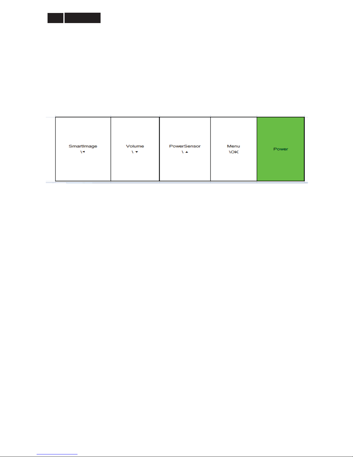
!
92
Meridian 3
use DDC-2B, DDC/CI, and EDID V1.3
DP Display identification
DDC /CI Support and Smart Manage/Control
In accordance with VESA DDC/CI and MCCS ver.2.0, the monitor should be workable with ,
Philps SmartManage, SmartControl V6.1, and Protrait Display Tune at least.
Pivot function(Auto pivot)
It needs to support AUTO PIVOT function with SmartControl PC application tool.
Hot-key definition
Refer to hot-key definition
Smart contrast Smart Contrast is a kind of dynamic backlight control.
This function changes the panel backlight dynamically according to the frame brightness histogram.
At least the minimum contrast ratio has to be> 20M:1 (Typ.)
Smart image
Attached Smart image file.
3.17 Modify PerfectTune
1.PER PERFECTTUNE MUST BE DONE AFTER WARMING 30 MINUTES AT
LEAST.
2.PERFECTTUNE MUST BE PERFORMED AFTER AUTO COLOR.
3.PERFECTTUNE MUST BE CONDUCTED THROUGH DVI OR SCALER
EMBEDDED P ATTERNS.
4.DELTA E < 10
Audio (Optional)
3.18.1 Frequency Response
The amplifier and speaker combination shall provide a frequency response of 300 Hz
to 20 kHz, with +/- 3 dB variation over the entire response range.
3.18.2 Total Harmonic Distortion
Total harmonic distortion shall be limited to 5% THD at the maximum wattage
speaker rating specified in section 1.3, at 1 kHz, when the input is 1.3Vrms.
3.18.3 Power Handling
Each speaker transducer shall accept up to the specified Wattage of audio power
without damage or exceeding the frequency response and total harmonic distortion
specifications.

Meridian 3
93
3.18.4 Audio Amplifier
The amplifier shall provide two channels of audio up to 2.0 Watts per channel from
100 Hz to 20 kHz, based upon an audio signal input of 1.0V RMS per channel.
3.18.5 Volume Control
For monitors with a manual volume control, the direction (at the bottom) of the bezel
volume control is “-“ key for Minimum volume and “+” key for Maximum volume. The
default shipping position of the Volume Control shall be approximately 90%.
3.18.6 Speaker Sensitivity
The speakers shall support a minimum sensitivity of 75 dB +/- 3 dB at 2W/1m at 1 kHz.
3.18.7 Maximum Audio Card Output
The monitor audio amplifier shall accept a maximum input voltage of 1.5 Vrms and
meet the following requirements at the maximum monitor volume setting:
1. The ratings of the audio amplifier may not be exceeded.
2. The ratings of the speakers may not be exceeded.
3. There must not be any clipping of the audio amplifier output signal.
Voltage dividers may be used to reduce the input signal level.
3.18.8 Monitor Audio Amplifier Input Impedance
The monitor audio amplifier shall have minimum 10K Ohm AC input impedance
3.19 USB HUB 2.0 support
Connect the HUB port of the monitor to host PC’s USB port via USB cable,
Then attach external device to the downstream port of the monitor.
Check if the device can work properly.
3.20 POWER SENSOR
UNCTIONAL Requirements for the front detection
For the presence sensor functionality, the following requirements are defined:
x Two IRs be used for user present detections, one IR is for transmission signals, the other one is for
receiving reflection IR signals
x User must be detected in the following range:
40 up to 100 cm (+ 20cm).
x Detection angle:
+- 30 degree (for IR LED )
x SENSOR key control,
Adjust detection distances (0~4 scales), default is 3 , tolerance : (±10cm)
0 : 0FF
1 : 90 cm tolerance : (±10cm)
2 : 100 cm tolerance : (±10cm)
3 : 110 cm tolerance : (±10cm)
4 : >130 cm
x Sensor test around condition (about lamp lighting)
a. Don’t this lamp lighting site :
i. ii.
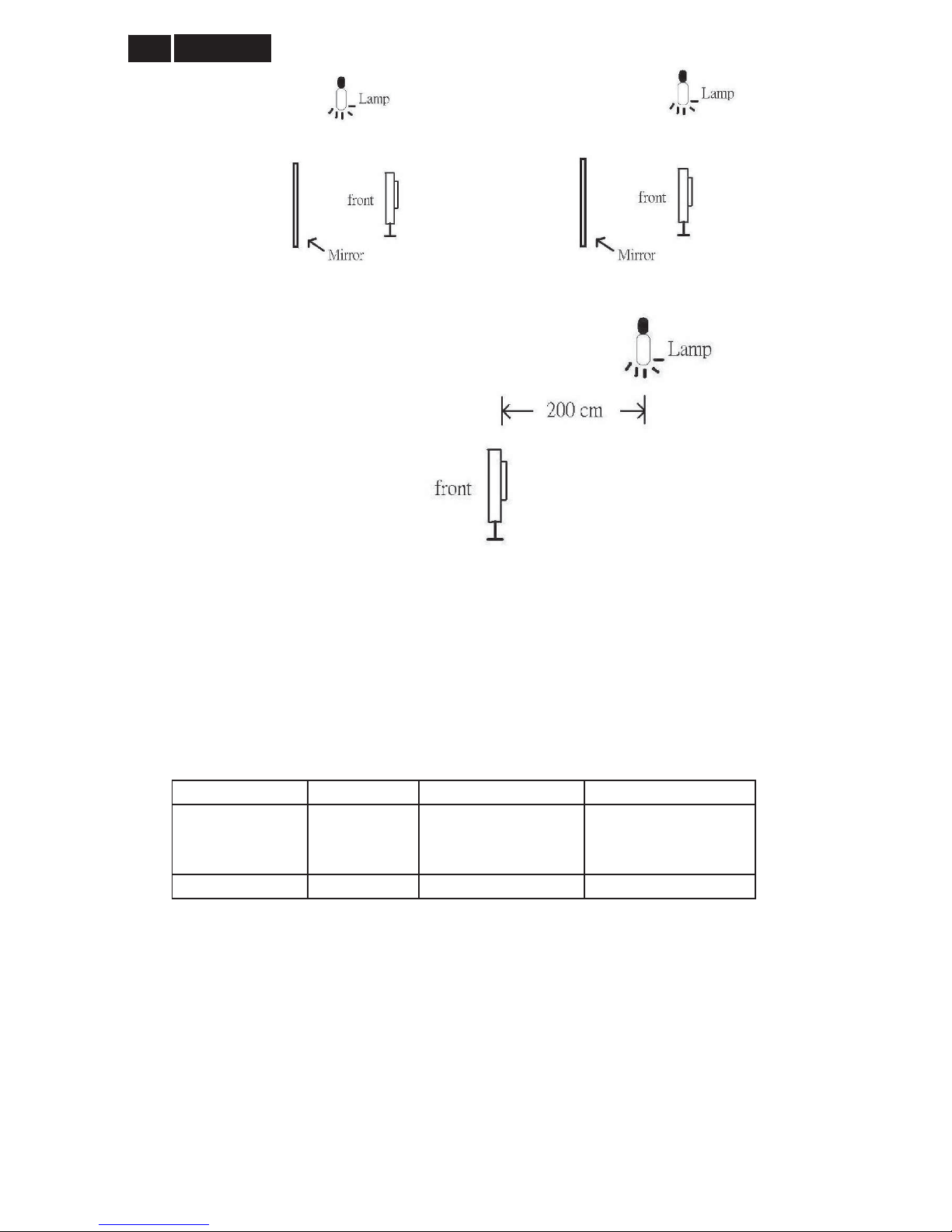
!
94
Meridian 3
b. Press set this lamp lighting site :
x SENSOR distance measure :
1. Cotton material color : black
2. Monitor center straight distance (90 deg)
3. Body width : about 40cm
4. Body horizontal move : Monitor center +- 5cm
x Anti-interference between two monitors,
Monitors must have anti-interference methods(coding ..etc) to prevent monitors to talk to each
other
power sensor Functional behavior
Time Period 60sec 60sec ~ 180sec 180se c ~
PowerSensor No ACTION
Lower down backlight
brightness
Backlight & LCD panel
shutdown
Power Saving 0 50% 80%

Meridian 3
95
The following set-up’s will be supported:
Monitor 1
Monitor 2
Top view
User 1
User 2
Fig. 2: 2 monitors standing back to back.
The monitors may influence each other. So Monitor 1 may produce unexpected
brightness-switches in monitor 2 (and vice versa). Furthermore, user 1 could perhaps (via
monitor 1) influence the powersensor readout on monitor 2.
Fig. 3: set up of multiple monitors under an angle
.

!
96
Meridian 3
Factory requirements
Factory requirements are taken into account.
It needs to do calibration to make sure the same detection distance.
Service requirements
Service requirements are taken into account.
In the factory mode, it needs to reserve the max. distance adjustment value to adjust
distance ranges.
3.21 Webcam : (optional)
Follow Wbcam spec, video transfer at USB HUB.
VISUAL CHARACTERISTICS
Test conditions
Unless otherwise specified, this specification is defined
under the following conditions.
(1) Input signal : As defined in 3.3, follow panel resolution,
signal sources must have 75 ohm
output impedance.
(2) Luminance setting : controls to be set to 300 nits with full screen 100 % duty cycle white
signal
(3) Warm up: more than 30 minutes after power on with signal supplied.
(4) Ambient light: 400 -- 600 lux.
(5) Ambient temperature: 20 ± 5 qC
Brightness
Follow Panel specification.
Image size
Actual display size : Follow panel spec.
Brightness uniformity
Set contrast at 100% and turn the brightness to get average above 300 nits at centre of
the screen.
Apply the Fig 1, it should comply with the following formula:
( B_max - B_min )
X 100% > 75%
B_max
Where B_max = Maximum brightness
B_min = Minimum brightness
Check Cross talk (S)
Apply Pattern 2. Set contrast and brightness at 100 %.
Measure YA. Then output Pattern 3 and measure YB.
the cross talk value :
ABS ( YA - YB )
X 100% < 1.5 %
YA
Color temperature adjustment
There are six factory preset white color 11500K,9300K,8200K,7500K 6500K,5000K
Apply full white pattern, with brightness in 100 % position and the contrast control at 50 % position.

Meridian 3
97
The 1931 CIE Chromaticity (color triangle) diagram (x ,y) coordinate for the screen center should be:
Product specification
CIE coordinates (x,y)
1 1500K x = 0.270 ± 0.02
y = 0.281 ± 0.02
PerfecTune II
9300K x = 0.283 ± 0.02
y = 0.297 ± 0.02
PerfecTune II
8200K x = 0.291 ± 0.02
y = 0.306 ± 0.02
PerfecTune II
7500K x = 0.298 ± 0.02
y = 0.314 ± 0.02
PerfecTune II
6500K/sRGB x = 0.313 ± 0.02
y = 0.329 ± 0.02
PerfecTune II
sRGB x = 0.313 ± 0.02
y = 0.329 ± 0.02
PerfecTune II
5000K x = 0.345 ± 0.02
y = 0.357 ± 0.02
PerfecTune II
Production alignment spec.
CIE coordinates (x,y)
1 1500K x = 0.270 ± 0.006
y = 0.281 ± 0.006
PerfecTune II
9300K x = 0.283 ± 0.006
y = 0.297 ± 0.006
PerfecTune II
8200K x = 0.291 ± 0.006
y = 0.306 ± 0.006
PerfecTune II
7500K x = 0.298 ± 0.006
y = 0.314 ± 0.006
PerfecTune II
6500K/sRGB x = 0.313 ± 0.006
y = 0.329 ± 0.006
PerfecTune II
sRGB x = 0.313 ± 0.006
y = 0.329 ± 0.006
PerfecTune II
5000K x = 0.345 ± 0.006
y = 0.357 ± 0.006
PerfecTune II
Quality Inspection specification:
CIE coordinates (x,y)
9300K x = 0.283 ± 0.015
y = 0.297 ± 0.015
6500K/sRGB x = 0.313 ± 0.015
y = 0.329 ± 0.015
sRGB x = 0.313 ± 0.015
y = 0.329 ± 0.015

!
98
Meridian 3
MECHANICAL CHARACTERISTICS
Cosmetic -
Philips ID
Mechanical data files -
ProE files required
Location of Philips logo -
Per Philips make-up sheet
Gap between panel and front bezel
< 1.2mm (Typ.)
Location of Control icons -
Per Philips Graphic sheet
Color for resin/paint -
Per Philips make-up sheet
Fire enclosure request
Shielding Cover should fulfill international standard
Resins
x RoHS required
x WEEE required.
x Resin type/selection refer to Project Book Section 7.2 Plastic material.
If paint is used
x RoHS required
x WEEE require
x If new painting type need to implement, refer to UN-D 1235.
Plastic mold tooling
x Tooling to be designed to minimize cosmetic defects induced by molding process (sink, blush,
weld lines, gate marks, ejector marks, etc.). Refer to “TYV61-90007”.
x Painting to cover up cosmetic defects due to molding is strongly discouraged.
x China RoHS mark requested.
Plastics flammability
x
All Plastics to be Flame Retardant UL 94-HB or Better.
x Base / Pedestal to be Flame Retardant UL 94-HB.
x All major plastic parts (bezel, back cover) need to be molded from same resin.
x Plastic resin type selection should be referred to “plastic-Philips Pool monitor”.
Texture/Glossing of housing
x The texture area and texture no should follow Philips make-up sheet.
x The exterior surfaces shall have a uniform texture.
x Philips must approve the mold texturing.
x Detail document for texture refer to “UN-D249”, “UN-D 600”.
x < = 20 gloss units

Meridian 3
99
Tilt and swivel base
x Tilt angle : -5 q +2/- 0 q (forward)
+20 q+ 0/- 3 q (backward)
x Swivel angle : nil
x High Adjustment : nil
x Portrait Display : nil
Kensington Lock
x Must meet Kensington_slot.spec “TYE-M0004”.
x MMD request metal plate in Kensington hole.
Label
x Regulatory label / Carton label should follow Philips requirement.
x China RoHS label
x Detail document refer to Philips Engineering Reference Book.
Product dimension / Weight ( Refer to Philips approved SHT 191/SHT560 )
x Unit dimension :
x Packed unit dimension:
x Net weight :
x Gross weight :
Transportation
Transportation standards refer to UAN-D1534/00/01/02.
Transportation packages
x Net weight Packaging and wrapping shall be sufficient to protect the product against damage
or loss during shipment from the supplier to the destination specified in the purchase order.
All packaging materials are subject to test and evaluation per UAN-D1534/00/01/02.
x The cushion material shall be constructed using EPS material.
x The doggy hole is requested.
Transportation Test
Overall tests refer to UAN-D1534/00/01/02.
Vibration, drop test should be performed at ambient temperature (20°C to 23
o
C) and relative
humidity (40% to 65%).
A. Transportation test specification for all regions
x Package test
1. Random Vibration test
2. Drop test
3. Cold Drop test (for design reference)
x Un-package test
1. Half sine shock test (non operation)
B. Transportation test specification for China/India
x Package test

!
100
Meridian 3
1. Random Vibration test
2. Drop test
3. Cold Drop test (for design reference)
x Un-package test
1. Sine vibration (operating)
2. Half sine shock test (non operation)
Pallet / Container loading (Refer to Philips approved SHT 560)
Transportation standards refer to TYE-M0002 ,UAN-D1534 and UAW-0309.
x Air shipment -
x Sea container 20'(pallet/slip sheet)
x Sea container 40'(pallet/slip sheet)
x Sea container 40' High Cube (pallet/slip sheet)
x Land 45‘ Truck and Trailer (800X1200mm pallet)
x Land 45‘ Truck and Trailer (1000X1200mm pallet) for UK
x Truck shipment-
Transportation request for all regions except China/India
A. Air shipment
B. 20’/40’/40’HQ Container loading for WW
Transportatio n request for China and India
A. Container loading for China and India
B. Truck loading
Transportatio n request for EU
A. Land 45‘ Truck and Trailer (800X1200mm pallet)
B. Land 45‘ Truck and Trailer (1000X1200mm pallet) for UK
ENVIRONMENTAL CHARACTERISTICS
The following sections define the interference and susceptibility condition limits that might occur
between external environment and the display device.
Susceptibility of display to external environment
Operating
- Temperature : 0 to 40 degree C
- Humidity : 80% max
- Altitude : 0-3658m
- Air pressure : 600-1100 mBAR
Storage
- Temperature : -20 to 60 degree C
- Humidity : 95% max
- Altitude : 0-12192m
- Air pressure : 300-1100 mBAR
Note: recommend at 5 to 35qC, Humidity less than 60 %
Transporta tion tests
Refer to 5.15.2
 Loading...