

Page 1

Colour Television Chassis
TE3.2E
CA
G_16010_000.eps
260406
Contents Page Contents Page
1. Technical Specifications, Connections and Chassis
Overview 2
2. Safety Instructions, Warnings, and Notes 5
3. Directions for Use 7
4. Mechanical Instructions 8
5. Service Modes, Error Codes and Fault Finding 9
6. Block Diagrams, Test Point Overviews, and
Waveforms
Block Diagram Audio / Video 11
Block Diagram Power Supply 12
I2C Diagram 13
Block Diagram 13
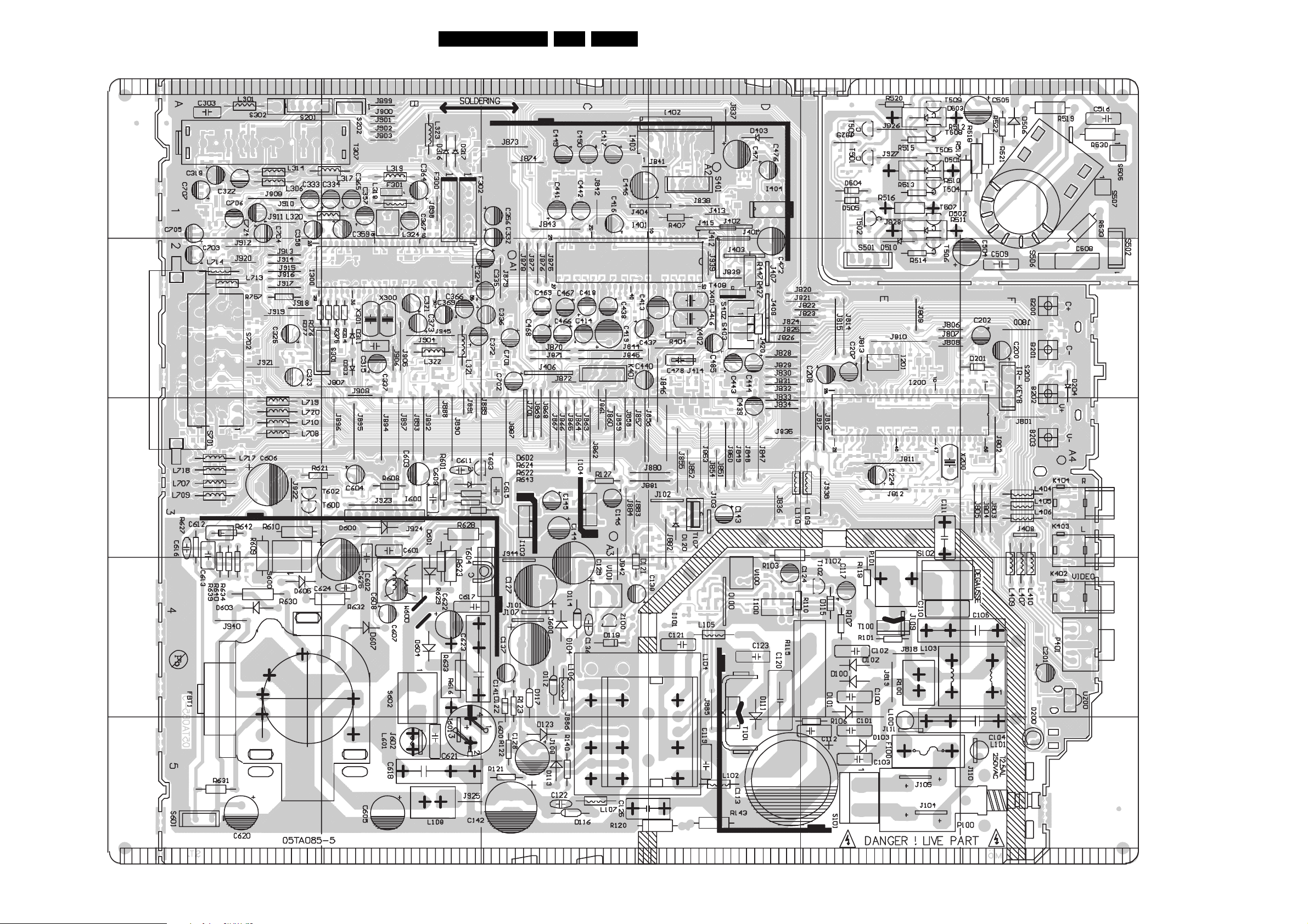
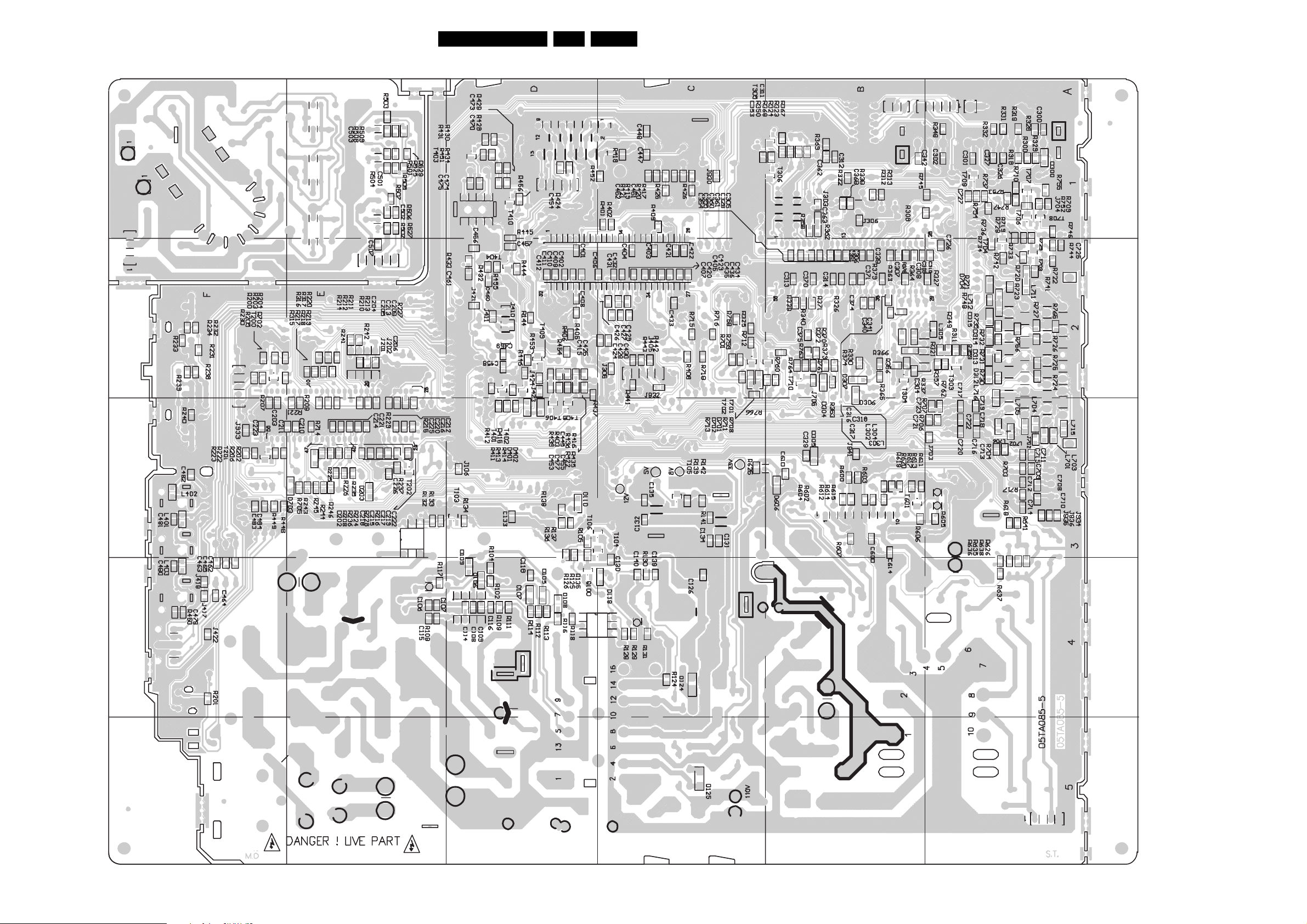
7. Circuit Diagrams and PWB Layouts Diagram PWB
Main Panel (05TA085-5): MCU (A1) 16 23-24
Main Panel (05TA085-5): Video (A2) 17 23-24
Main Panel (05TA085-5): Sound (A3) 18 23-24
Main Panel (05TA085-5): Power (A4) 19 23-24
Main Panel (05TA085-5): Deflection (A5) 20 23-24
CRT Panel (05TA085-5) (A6)21 23-24
Main Panel (05TA085-5): SCART (A7) 25 23-24
Main Panel (05TA085-6): MCU (A1) 25 32-33
Main Panel (05TA085-6): Video (A2) 26 32-33
Main Panel (05TA085-6): Sound (A3) 27 32-33
Main Panel (05TA085-6): Power (A4) 28 32-33
Main Panel (05TA085-6): Deflection (A5) 29 32-33
CRT Panel (05TA085-6) (A6)30 32-33
Main Panel (05TA085-6): SCART (A7) 31 32-33
Side I/O Panel (21PT5421 only) (A8) 34 35
8. Alignments 37
9. Circuit Descriptions, Abbreviation List, and IC Data
Sheets 39
Abbreviation List 42
IC Data Sheets 43
10. Spare Parts List 51
11. Revision List 78
©
Copyright 2006 Philips Consumer Electronics B.V. Eindhoven, The Netherlands.
All rights reserved. No part of this publication may be reproduced, stored in a
retrieval system or transmitted, in any form or by any means, electronic,
mechanical, photocopying, or otherwise without the prior permission of Philips.
Published by JH 0664 BG CD Customer Service Printed in The Netherlands Subject to modification EN 3122 785 16011
Page 2
EN 2 TE3.2E CA1.
Technical Specifications, Connections and Chassis Overview
1. Technical Specifications, Connections and Chassis Overview
Index of this chapter:
1.1 Technical Specifications
1.2 Connections / Control Facilities
1.3 Chassis Overview
1.1 Technical Specifications
1.1.1 Reception
Tuning system : PLL
Colour systems : PAL B/G, D/K, I
: SECAM B/G, L/L'
Sound systems 14” : Mono
Sound systems 21” : Mono
: Nicam B/G, D/K, I, L
A/V connections : NTSC 3.58
: NTSC 4.43
Channel selections : 100 channels
: UVSH
IF frequency : Systems B/G, D/K, L,
I: 38.9 MHz
: System L': 33.95 MHz
Aerial input : 75 Ω, Coax
1.1.2 Miscellaneous
Audio output (RMS) 14” : 1x 1 W Mono
Audio output (RMS) 21” : 1x 4W Mono
: 2x 3 W Mono
Mains voltage : 220 - 240 V
Mains frequency : 50 Hz
Ambient temperature : + 5 to + 45 deg. C
Maximum humidity : 90 %
Power consumption : 50 W (10 %)
Standby Power consumption : < 2 W
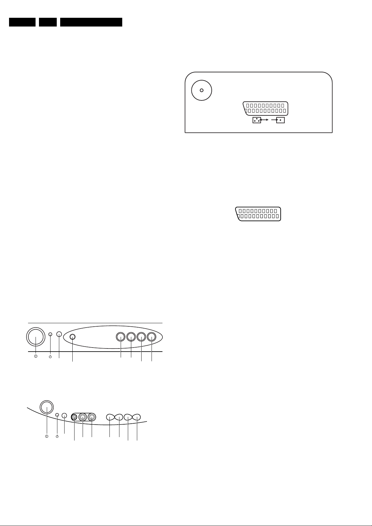
1.2 Connections / Control Facilities
1.2.1 Front Connections and Front Control
1.2.2 Rear Connections 14” & 21”
75 Ohm
EXT1
Figure 1-3 Rear Connections
TV Aerial In
Aerial input : 75 Ω, Coax (IEC-
type)
External 1: RGB in + CVBS in/out
20
21
2
E_06532_001.eps
050404
1
Figure 1-4 SCART connector
1 -Audio R (0.5 V
2 -Audio R (0.5 V
3 - Audio L (0.5 V
4 - GND H
1 kΩ) k
rms
10 kΩ) j
rms
1 kΩ) k
rms
5 - GND H
6 - Audio L (0.5 V
7 - Blue (0.7 Vpp / 75 Ω) j
10 kΩ) j
rms
8 - CVBS-status 0 - 2.0 V: INT
4.5 - 12 V: EXT 4:3
9 - GND H
10 -
F_15850_002.eps
160805
SK1 RED
IR
HEADPHONE
- VOLUME +
- PROGRAM +
G_16010_013.eps
Figure 1-1 Front Control without AV Input (xxPT1501)
SK1
RED
VIDEO
- VOLUME + AUDIO
- PROGRAM +HEADPHONE
G_16010_014.eps
130206
IR
Figure 1-2 Front Control with AV Input (xxPT1521)
Audio / Video In (Only for 14PT1521)
1 -Video CVBS (1 V
2 -Audio (MONO) (0.5 V
3 -Headphone 3.5 mm (8 - 600 Ω/ <100 mW) rt
/ 75 Ω) jq
pp
/ 10 k Ω) jq
rms
130206
11 - Green (0.7 V
12 -
/ 75 Ω) j
pp
13 - GND H
14 - GND H
15 - Red (0.7 V
16 - RGB-status 0 - 0.4 V: INT
/ 75 Ω) j
PP
1 - 3 V: EXT / 75 Ω
17 - GND H
18 - GND H
19 - CVBS (1 V
20 - CVBS (1 V
21 - Earth GND vj
/ 75 Ω) k
pp
/ 75 Ω) j
pp
Page 3
Technical Specifications, Connections and Chassis Overview
EN 3TE3.2E CA 1.
1.2.3 Rear Connections 21PT5421 only
75 Ohm
Figure 1-5 Rear Connections
TV Aerial In
Aerial input : 75 Ω, Coax (IEC-
External 1: RGB/YUV - In and CVBS - In/Out
20
21
2
E_06532_001.eps
050404
1
type)
G_16010_040.eps
260406
8 - CVBS - status 0 - 2 V: INT
4.5 - 7 V: EXT 16:9
9.5 - 12 V: EXT 4:3
9 - Green - gnd Ground H
10 - n.c.
11 - n.c.
12 - n.c.
13 - Red - gnd Ground H
14 - FBL - gnd Ground H
15 - YC-C - in 0.7 V_pp / 75 ohm j
16 - n.c.
17 - Video Ground H
18 - Video Ground H
19 - CVBS - out 1 V_pp / 75 ohm k
20 - Y/CVBS - in 1 V_pp / 75 ohm j
21 - Shielding Ground H
1.2.4 Side Connections 21PT5421 only
Figure 1-6 SCART connector
1 - Audio - R 0.5 V_rms / 1 kohm k
2 - Audio - R 0.5 V_rms / 10 kohm j
3 - Audio - L 0.5 V_rms / 1 kohm k
4 - Audio - gnd Ground H
5 - Blue - gnd Ground H
6 - Audio - L 0.5 V_rms / 10 kohm j
7 - Blue/U - in 0.7 V_pp / 75 ohm j
8 - CVBS - status 0 - 2 V: INT
4.5 - 7 V: EXT 16:9
9.5 - 12 V: EXT 4:3
9 - Green - gnd Ground H
10 - n.c.
11 - Green/Y - in 0.7 V_pp / 75 ohm j
12 - n.c.
13 - Red - gnd Ground H
14 - FBL - gnd Ground H
15 - Red/V - in 0.7 V_pp / 75 ohm j
16 - Status/FBL 0 - 0.4 V: INT
1 - 3 V: EXT / 75 ohm j
17 - Video Ground H
18 - Video Ground H
19 - CVBS - out 1 V_pp / 75 ohm k
20 - CVBS - in 1 V_pp / 75 ohm j
21 - Shielding Ground H
External 2: CVBS- In and SVHS - In
20
2
G_16010_041.eps
260406
Audio / Video In
Ye - Video (CVBS) 1 V_pp / 75 ohm jq
Wh - Audio - L 0.5 V_rms / 10 kohm jq
Rd - Audio - R 0.5 V_rms / 10 kohm jq
Bk - Headphone 8 - 600 Ohm / 4 mW ot
21
E_06532_001.eps
050404
1
Figure 1-7 SCART connector
1 - Audio - R 0.5 V_rms / 1 kohm k
2 - Audio - R 0.5 V_rms / 10 kohm j
3 - Audio - L 0.5 V_rms / 1 kohm k
4 - Audio - gnd Ground H
5 - Blue - gnd Ground H
6 - Audio - L 0.5 V_rms / 10 kohm j
7-n.c.
Page 4
EN 4 TE3.2E CA1.
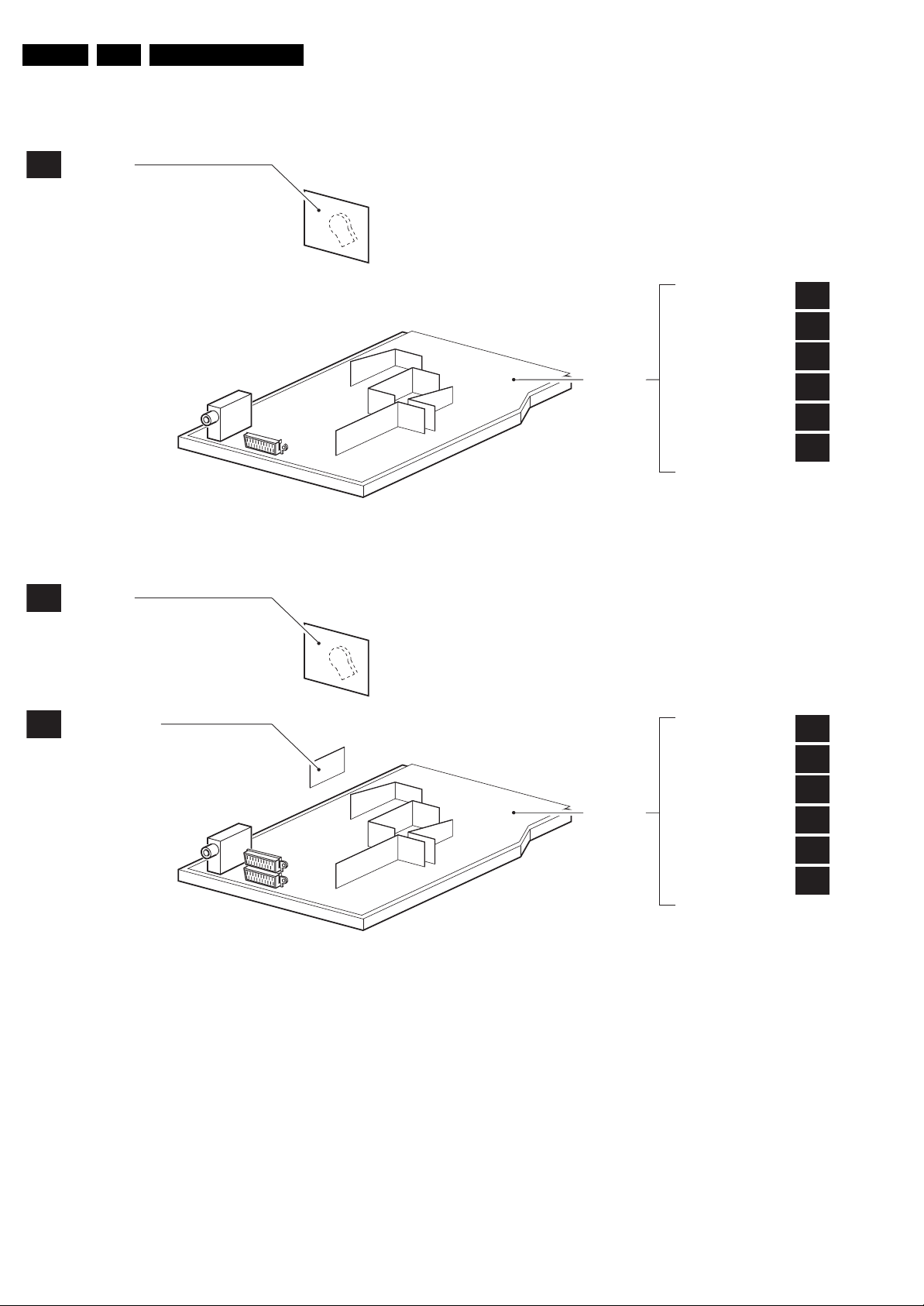
1.3 Chassis Overview
CRT PANEL
A6
Technical Specifications, Connections and Chassis Overview
CRT PANEL
A6
SIDE I/O PANEL
A8
Figure 1-8 Chassis Overview 14” & 21”
MAIN
CHASSIS
PANEL
MCU
VIDEO
SOUND
POWER
DEFLECTION
SCART
MCU
A1
A2
A3
A4
A5
A7
G_16010_042.eps
260406
A1
Figure 1-9 Chassis Overview 21PT5421
MAIN
CHASSIS
PANEL
VIDEO
SOUND
POWER
DEFLECTION
SCART
A2
A3
A4
A5
A7
G_16010_043.eps
260406
Page 5
Safety Instructions, Warnings, and Notes
2. Safety Instructions, Warnings, and Notes
EN 5TE3.2E CA 2.
Index of this chapter:
2.1 Safety Instructions
2.2 Maintenance Instructions
2.3 Warnings
2.4 Notes
2.1 Safety Instructions
Safety regulations require the following during a repair:
• Connect the set to the Mains/AC Power via an isolation
transformer (> 800 VA).
• Replace safety components, indicated by the symbol h,
only by components identical to the original ones. Any
other component substitution (other than original type) may
increase risk of fire or electrical shock hazard.
• Wear safety goggles when you replace the CRT.
Safety regulations require that after a repair, the set must be
returned in its original condition. Pay in particular attention to
the following points:
• General repair instruction: as a strict precaution, we advise
you to re-solder the solder connections through which the
horizontal deflection current flows. In particular this is valid
for the:
1. Pins of the line output transformer (LOT).
2. Fly-back capacitor(s).
3. S-correction capacitor(s).
4. Line output transistor.
5. Pins of the connector with wires to the deflection coil.
6. Other components through which the deflection current
flows.
Note: This re-soldering is advised to prevent bad connections
due to metal fatigue in solder connections, and is therefore only
necessary for television sets more than two years old.
• Route the wire trees and EHT cable correctly and secure
them with the mounted cable clamps.
• Check the insulation of the Mains/AC Power lead for
external damage.
• Check the strain relief of the Mains/AC Power cord for
proper function, to prevent the cord from touching the CRT,
hot components, or heat sinks.
• Check the electrical DC resistance between the Mains/AC
Power plug and the secondary side (only for sets that have
a Mains/AC Power isolated power supply):
1. Unplug the Mains/AC Power cord and connect a wire
between the two pins of the Mains/AC Power plug.
2. Set the Mains/AC Power switch to the "on" position
(keep the Mains/AC Power cord unplugged!).
3. Measure the resistance value between the pins of the
Mains/AC Power plug and the metal shielding of the
tuner or the aerial connection on the set. The reading
should be between 4.5 Mohm and 12 Mohm.
4. Switch "off" the set, and remove the wire between the
two pins of the Mains/AC Power plug.
• Check the cabinet for defects, to prevent touching of any
inner parts by the customer.
2.2 Maintenance Instructions
We recommend a maintenance inspection carried out by
qualified service personnel. The interval depends on the usage
conditions:
• When a customer uses the set under normal
circumstances, for example in a living room, the
recommended interval is three to five years.
• When a customer uses the set in an environment with
higher dust, grease, or moisture levels, for example in a
kitchen, the recommended interval is one year.
• The maintenance inspection includes the following actions:
1. Perform the “general repair instruction” noted above.
2. Clean the power supply and deflection circuitry on the
chassis.
3. Clean the picture tube panel and the neck of the picture
tube.
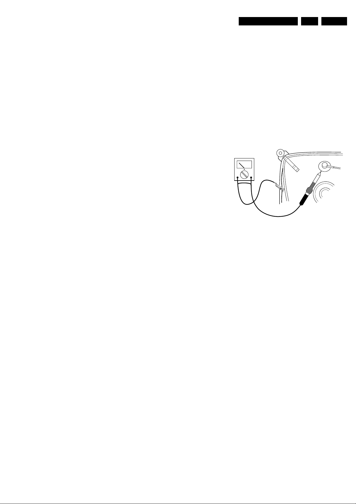
2.3 Warnings
• In order to prevent damage to ICs and transistors, avoid all
high voltage flashovers. In order to prevent damage to the
picture tube, use the method shown in figure “Discharge
picture tube”, to discharge the picture tube. Use a high
voltage probe and a multi-meter (position V
until the meter reading is 0 V (after approx. 30 s).
V
Figure 2-1 Discharge picture tube
• All ICs and many other semiconductors are susceptible to
electrostatic discharges (ESD w). Careless handling
during repair can reduce life drastically. Make sure that,
during repair, you are connected with the same potential as
the mass of the set by a wristband with resistance. Keep
components and tools also at this same potential. Available
ESD protection equipment:
– Complete kit ESD3 (small tablemat, wristband,
connection box, extension cable and earth cable) 4822
310 10671.
– Wristband tester 4822 344 13999.
• Be careful during measurements in the high voltage
section.
• Never replace modules or other components while the unit
is switched "on".
• When you align the set, use plastic rather than metal tools.
This will prevent any short circuits and prevents circuits
from becoming unstable.
2.4 Notes
2.4.1 General
• Measure the voltages and waveforms with regard to the
chassis (= tuner) ground (H), or hot ground (I), depending
on the tested area of circuitry. The voltages and waveforms
shown in the diagrams are indicative. Measure them in the
Service Default Mode (see chapter 5) with a colour bar
signal and stereo sound (L: 3 kHz, R: 1 kHz unless stated
otherwise) and picture carrier at 475.25 MHz for PAL, or
61.25 MHz for NTSC (channel 3).
• Where necessary, measure the waveforms and voltages
with (D) and without (E) aerial signal. Measure the
voltages in the power supply section both in normal
operation (G) and in stand-by (F). These values are
indicated by means of the appropriate symbols.
• The semiconductors indicated in the circuit diagram and in
the parts lists, are interchangeable per position with the
). Discharge
DC
E_06532_007.eps
250304
Page 6

EN 6 TE3.2E CA2.
Safety Instructions, Warnings, and Notes
semiconductors in the unit, irrespective of the type
indication on these semiconductors.
2.4.2 Schematic Notes
• All resistor values are in ohms, and the value multiplier is
often used to indicate the decimal point location (e.g. 2K2
indicates 2.2 kohm).
• Resistor values with no multiplier may be indicated with
either an "E" or an "R" (e.g. 220E or 220R indicates 220
ohm).
• All capacitor values are given in micro-farads (µ= x10
nano-farads (n= x10
• Capacitor values may also use the value multiplier as the
decimal point indication (e.g. 2p2 indicates 2.2 pF).
• An "asterisk" (*) indicates component usage varies. Refer
to the diversity tables for the correct values.
• The correct component values are listed in the Spare Parts
List. Therefore, always check this list when there is any
doubt.
2.4.3 Rework on BGA (Ball Grid Array) ICs
General
Although (LF)BGA assembly yields are very high, there may
still be a requirement for component rework. By rework, we
mean the process of removing the component from the PWB
and replacing it with a new component. If an (LF)BGA is
removed from a PWB, the solder balls of the component are
deformed drastically so the removed (LF)BGA has to be
discarded.
-9
), or pico-farads (p= x10
-12
2.4.4 Lead-free Solder
Philips CE is producing lead-free sets (PBF) from 1.1.2005
onwards.
Identification: The bottom line of a type plate gives a 14-digit
serial number. Digits 5 and 6 refer to the production year, digits
7 and 8 refer to production week (in example below it is 1991
week 18).
-6
),
).
E_06532_024.eps
230205
Figure 2-2 Serial number example
Regardless of the special lead-free logo (which is not always
indicated), one must treat all sets from this date onwards
according to the rules as described below.
P
b
Device Removal
As is the case with any component that is being removed, it is
essential when removing an (LF)BGA, that the board, tracks,
solder lands, or surrounding components are not damaged. To
remove an (LF)BGA, the board must be uniformly heated to a
temperature close to the reflow soldering temperature. A
uniform temperature reduces the risk of warping the PWB.
To do this, we recommend that the board is heated until it is
certain that all the joints are molten. Then carefully pull the
component off the board with a vacuum nozzle. For the
appropriate temperature profiles, see the IC data sheet.
Area Preparation
When the component has been removed, the vacant IC area
must be cleaned before replacing the (LF)BGA.
Removing an IC often leaves varying amounts of solder on the
mounting lands. This excessive solder can be removed with
either a solder sucker or solder wick. The remaining flux can be
removed with a brush and cleaning agent.
After the board is properly cleaned and inspected, apply flux on
the solder lands and on the connection balls of the (LF)BGA.
Note: Do not apply solder paste, as this has been shown to
result in problems during re-soldering.
Device Replacement
The last step in the repair process is to solder the new
component on the board. Ideally, the (LF)BGA should be
aligned under a microscope or magnifying glass. If this is not
possible, try to align the (LF)BGA with any board markers.
So as not to damage neighbouring components, it may be
necessary to reduce some temperatures and times.
More Information
For more information on how to handle BGA devices, visit this
URL: www.atyourservice.ce.philips.com (needs subscription,
not available for all regions). After login, select “Magazine”,
then go to “Repair downloads”. Here you will find Information
on how to deal with BGA-ICs.
Figure 2-3 Lead-free logo
Due to lead-free technology some rules have to be respected
by the workshop during a repair:
• Use only lead-free soldering tin Philips SAC305 with order
code 0622 149 00106. If lead-free solder paste is required,
please contact the manufacturer of your soldering
equipment. In general, use of solder paste within
workshops should be avoided because paste is not easy to
store and to handle.
• Use only adequate solder tools applicable for lead-free
soldering tin. The solder tool must be able:
– To reach a solder-tip temperature of at least 400°C.
– To stabilise the adjusted temperature at the solder-tip.
– To exchange solder-tips for different applications.
• Adjust your solder tool so that a temperature of around
360°C - 380°C is reached and stabilised at the solder joint.
Heating time of the solder-joint should not exceed ~ 4 sec.
Avoid temperatures above 400°C, otherwise wear-out of
tips will increase drastically and flux-fluid will be destroyed.
To avoid wear-out of tips, switch “off” unused equipment or
reduce heat.
• Mix of lead-free soldering tin/parts with leaded soldering
tin/parts is possible but PHILIPS recommends strongly to
avoid mixed regimes. If this cannot be avoided, carefully
clean the solder-joint from old tin and re-solder with new
tin.
• Use only original spare-parts listed in the Service-Manuals.
Not listed standard material (commodities) has to be
purchased at external companies.
• Special information for lead-free BGA ICs: these ICs will be
delivered in so-called "dry-packaging" to protect the IC
against moisture. This packaging may only be opened
shortly before it is used (soldered). Otherwise the body of
the IC gets "wet" inside and during the heating time the
structure of the IC will be destroyed due to high (steam-)
pressure inside the body. If the packaging was opened
before usage, the IC has to be heated up for some hours
(around 90°C) for drying (think of ESD-protection!).
Do not re-use BGAs at all!
Page 7

Directions for Use
EN 7TE3.2E CA 3.
• For sets produced before 1.1.2005, containing leaded
soldering tin and components, all needed spare parts will
be available till the end of the service period. For the repair
of such sets nothing changes.
In case of doubt whether the board is lead-free or not (or with
mixed technologies), you can use the following method:
• Always use the highest temperature to solder, when using
SAC305 (see also instructions below).
• De-solder thoroughly (clean solder joints to avoid mix of
two alloys).
Caution: For BGA-ICs, you must use the correct temperatureprofile, which is coupled to the 12NC. For an overview of these
profiles, visit the website www.atyourservice.ce.philips.com
(needs subscription, but is not available for all regions)
3. Directions for Use
You can download this information from the following websites:
http://www.philips.com/support
http://www.p4c.philips.com
You will find this and more technical information within the
"Magazine", chapter "Repair downloads".
For additional questions please contact your local repair help
desk.
2.4.5 Practical Service Precautions
• It makes sense to avoid exposure to electrical shock.
While some sources are expected to have a possible
dangerous impact, others of quite high potential are of
limited current and are sometimes held in less regard.
• Always respect voltages. While some may not be
dangerous in themselves, they can cause unexpected
reactions that are best avoided. Before reaching into a
powered TV set, it is best to test the high voltage insulation.
It is easy to do, and is a good service precaution.
Page 8
EN 8 TE3.2E CA4.
Mechanical Instructions
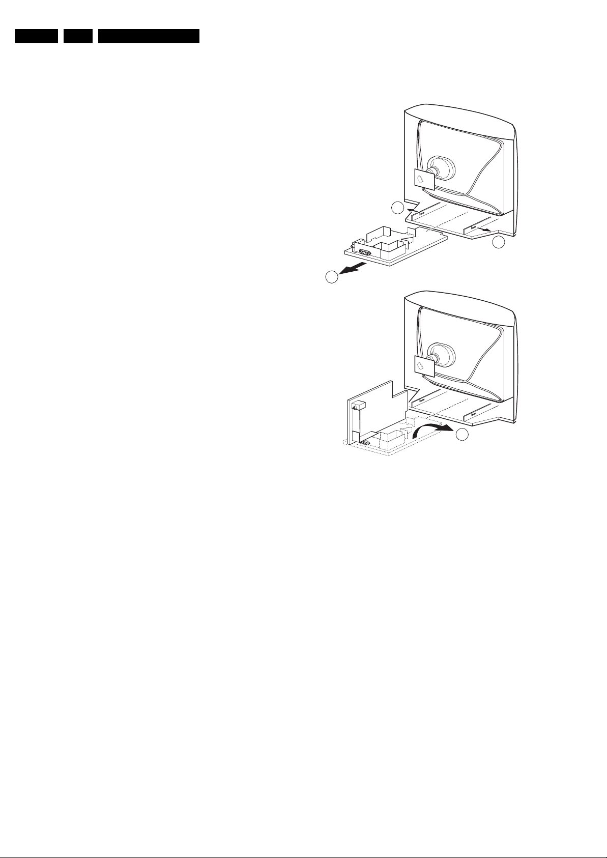
4. Mechanical Instructions
Index of this chapter:
4.1 Rear Cover Removal
4.2 Service Position Main Panel
4.3 Rear Cover Mounting
Note: Figures below can deviate slightly from the actual
situation, due to the different set executions.
4.1 Rear Cover Removal
• Remove all (ten) fixation screws of the rear cover: two at
the top, two at each side, three at the bottom and one in
the middle of the rear cover. The 14" set has only four
fixation screws: two at the top and two at the bottom.
• Now pull the rear cover backward to remove it.
4.2 Service Position Main Panel
• Disconnect the strain relief of the Mains cord.
• Remove the main panel, by pushing the two centre clips
outward [1]. At the same time, pull the panel away from the
CRT [2].
• Disconnect the degaussing coil by removing the cable from
connector KP02.
• Move the panel somewhat to the left and flip it 90 degrees
[3], with the components towards the CRT.
4.3 Rear Cover Mounting
Before you mount the rear cover:
• Place the mains cord correctly in its guiding brackets
(strain relief).
• Place all cables in their original position.
1
2
A
B
Figure 4-1 Mechanical Service Position
3
G_16010_010.eps
1
130206
Page 9

Service Modes, Error Codes and Fault Finding
5. Service Modes, Error Codes and Fault Finding
EN 9TE3.2E CA 5.
Index of this chapter:
5.1 Service Modes
5.2 Fault Tracing Diagram for Power Supply
5.1 Service Modes
The Service Mode offers features, which the service technician
can use to repair a set. Any feature change, made via the
Service Menu, will respond at the same time. All displayed text
strings in the Service Modes are in English.
5.1.1 TV Service Mode
Purpose
• To perform alignments (e.g. colour adjustment and
geometry alignments)
• To change option settings
Specifications
All service unfriendly modes (if present) are disabled, like:
• Auto switch 'off' (when there is no 'ident' signal)
• Timer switch to a channel
• Automatic user menu time-out
• The NVM is unprotected
• AV functions are not working
How to enter the Service Mode
Screen menu's must be 'off', when you enter the Service Mode.
Use a standard customer RC transmitter and key in the code
062596 directly followed by the MENU button in 10 seconds.
The following screen is visible when you enter the Service
Mode:
How to navigate
• Select menu items with the CURSOR UP/DOWN keys.
• With the CURSOR LEFT/RIGHT keys, it is possible to
change the value of the first item (Program)
• With the CURSOR RIGHT and OK keys, activate the
selected menu item.
• When you press the MENU key in a sub menu, you will
return to the previous menu.
• When you press the MENU key in the Service Mode menu,
you will return to the Main menu.
How to exit
• With the STANDBY command, the set switches to
Standby.
• With the MENU key, the set returns to the Main menu.
Switching the set 'off' and 'on' with the mains switch, brings
the set into normal operation again. All changes in the
Service Mode are stored immediately.
ST92195PSC7-V5 XX.XX.XX
Program 06
OPTIONS
GEOMETRY
G2A
VIDEO
TUNER/IF
G_16010_011.eps
130206
Figure 5-1 TV Service Mode Menu
1. LLLLLLL. This is the used IC type.
2. PAB#-XX. This is the software identification.
• P = Philips.
• A = the region (W = West Europe, E = East Europe).
• B = sound specification (M = Mono, S = Stereo).
• # = number of TXT pages.
• XX = the software version number (the first X is the
main software version number and the second X is the
sub software version number).
3. PROGRAM.
4. OPTIONS. Three codes possible.
5. GEOMETRY. To align the geometry (see chapter 8.2.2 for
a detailed description).
6. G2A. To align the G2 (see chapter 8.2.3 for a detailed
description).
7. VIDEO. To adjust RGB, R_cut-off and G_cut-off.
8. TUNER/IF. To align the tuner.
Page 10
EN 10 TE3.2E CA5.
Service Modes, Error Codes and Fault Finding
5.2 Fault Tracing Diagram for Power Supply
D100,101
D102,103
C106,
R100,
G_16010_013.eps
130206
YES
Fuse
F100
Defective
NO
Switched mode
Power Supply defective,
+110V is missing or level
is wrong
R107, R115
Open
circuit
R112
R110, D107
D106,R114
NO
YES
YES
Voltage at
drain of
T101
YES
Voltage at
I100 pin3
<1V
NO
Start-up
Voltage pin 8
<8V
NO
I101
NO
D116
NO
Control range of
switched-mode
Power Supply
Figure 5-2 Fault Tracing
Measure
+110V
adjustable
with V100
YES
G_16010_012.eps
130206
Page 11
Service Modes, Error Codes and Fault Finding
EN 11TE3.2E CA 5.
Table 5-1 Diversity between Main Board 05TA085-5 and 05TA085-6
Component Pos.No Type/Value Reason for Modification Schematic Location Action Component
J847 8MM Removed (D125 Will Be Used) A1 MCU removed jumper
J947 18MM Emc A2 Video New Jumper
J950 0R SMD Emc A2 Video New Jumper
J951 0R SMD Emc A2 Video New Jumper
L325 FB SMD Mute/demute Problem A2 Video New Inductor coil
D404 LL4148 Plop Sound Problem A3 Sound New Diode
D405 LL4148 Plop Sound Problem A3 Sound New Diode
J425 10MM Optional Jumper(Sound Output Balance) A3 Sound New Jumper
J948 18MM Plop Sound Problem A3 Sound New Jumper
R457 3K3 SMD Plop Sound Problem A3 Sound New Resistor
R458 10K SMD Plop Sound Problem A3 Sound New Resistor
R459 390R SMD Plop Sound Problem A3 Sound New Resistor
R460 1K SMD Plop Sound Problem A3 Sound New Resistor
R461 390R SMD Plop Sound Problem A3 Sound New Resistor
R462 10K SMD Plop Sound Problem A3 Sound New Resistor
R463 1K SMD Plop Sound Problem A3 Sound New Resistor
T411 BC848 Plop Sound Problem A3 Sound New Transistor
T412 BC848 Plop Sound Problem A3 Sound New Transistor
D125 BAT85 Fault Condition Tests A4 Power Change DIODE RECT.SS13 BAT85
R100 PRS05W Temperature Problem A4 Power Same Same
R147 Not Used A4 Power New Fuse
R148 FUSE,3A,32V,SMD Fault Condition Tests A4 Power New Fuse
C626 Fault Condition Tests(Not Used) A5 Deflection C626 (New) not used but added to schematic
J707 0R Optional Jumper A7 Scart New Jumper
J949 8MM Emc A7 Scart New Jumper
L721 10uH SMD Emc A7 Scart New inductor coil
J952 13MM Emc
Page 12

EN 12 TE3.2E CA5.
Personal Notes:
Service Modes, Error Codes and Fault Finding
E_06532_012.eps
131004
Page 13
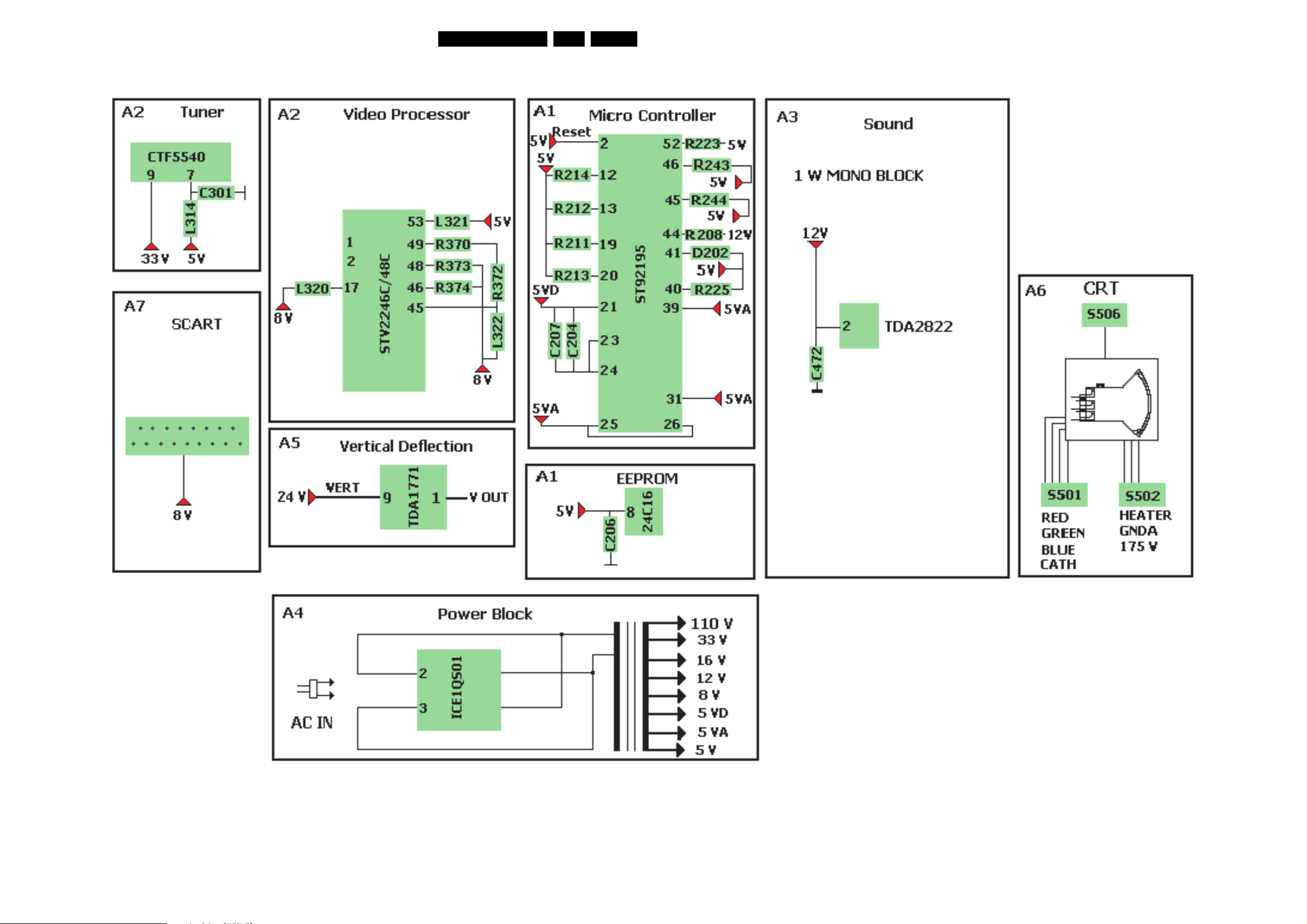
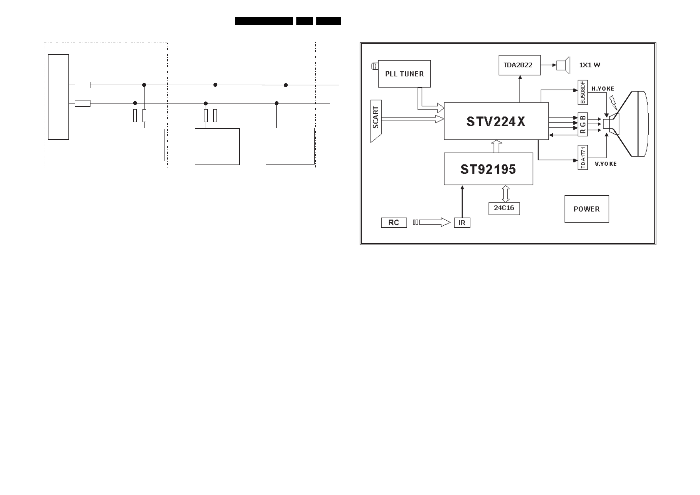
Block Diagrams, Test Point Overviews, and Waveforms
6. Block Diagrams, Test Point Overviews, and Waveforms
Block Diagram Audio / Video
EN 13TE3.2E CA 6.
G_16010_015.eps
130206
Page 14
Block Diagrams, Test Point Overviews, and Waveforms
Block Diagram Power Supply
EN 14TE3.2E CA 6.
G_16010_016.eps
130206
Page 15
Block Diagrams, Test Point Overviews, and Waveforms
EN 15TE3.2E CA 6.
I2C Diagram
2A
5
4
TUNER CTF5540
142R
242R
Block Diagram
1A
ADS
L
CS
043
R
933R
2515
OEDIV
.CORP
8422VTS
ADS
CS
L
242R
6
142R
5
MORPEE
61C42
ADS
LCS
9102
UCM
59129TS
G_16010_017.eps
130206
G_16010_018.eps
130206
Page 16
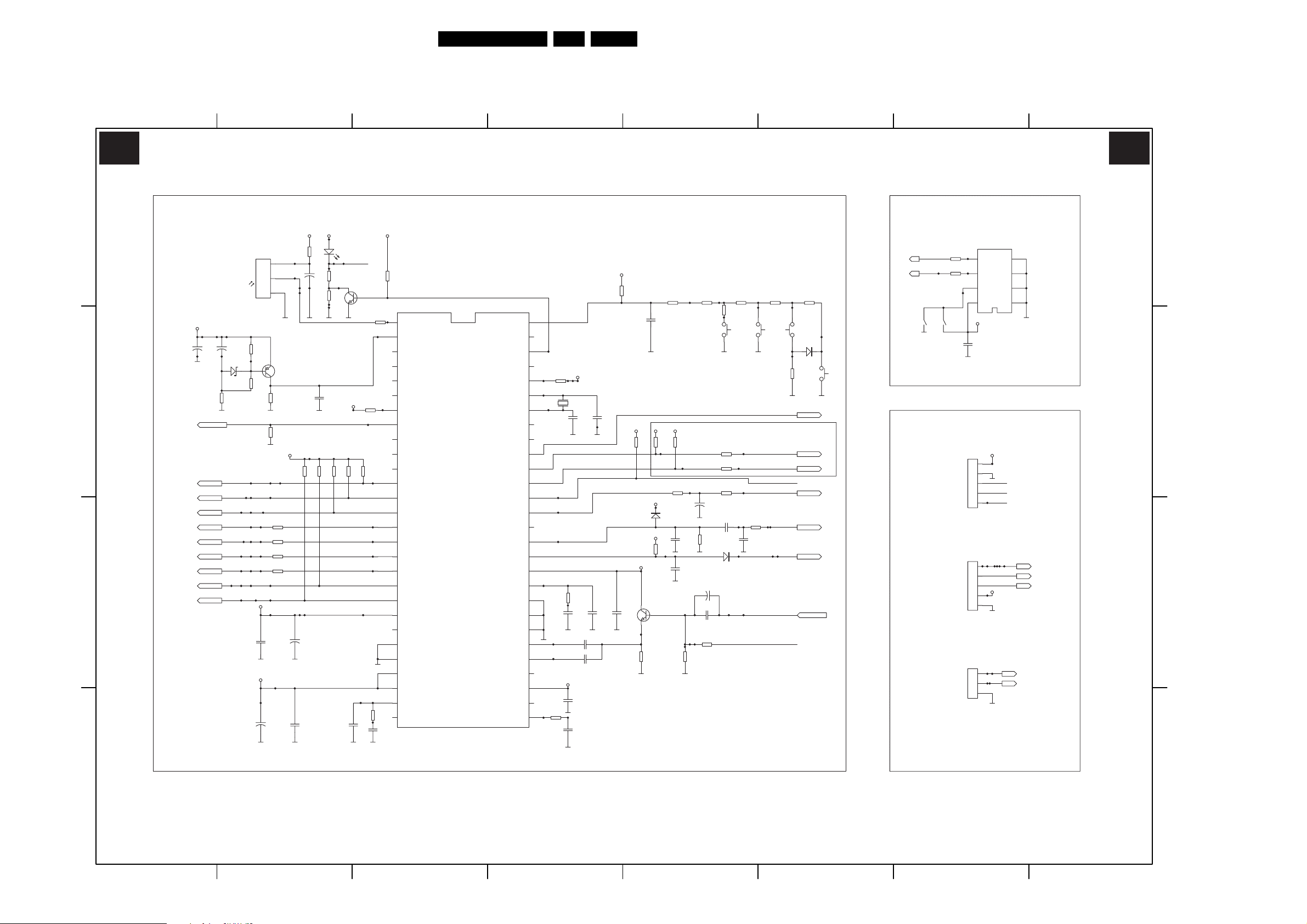
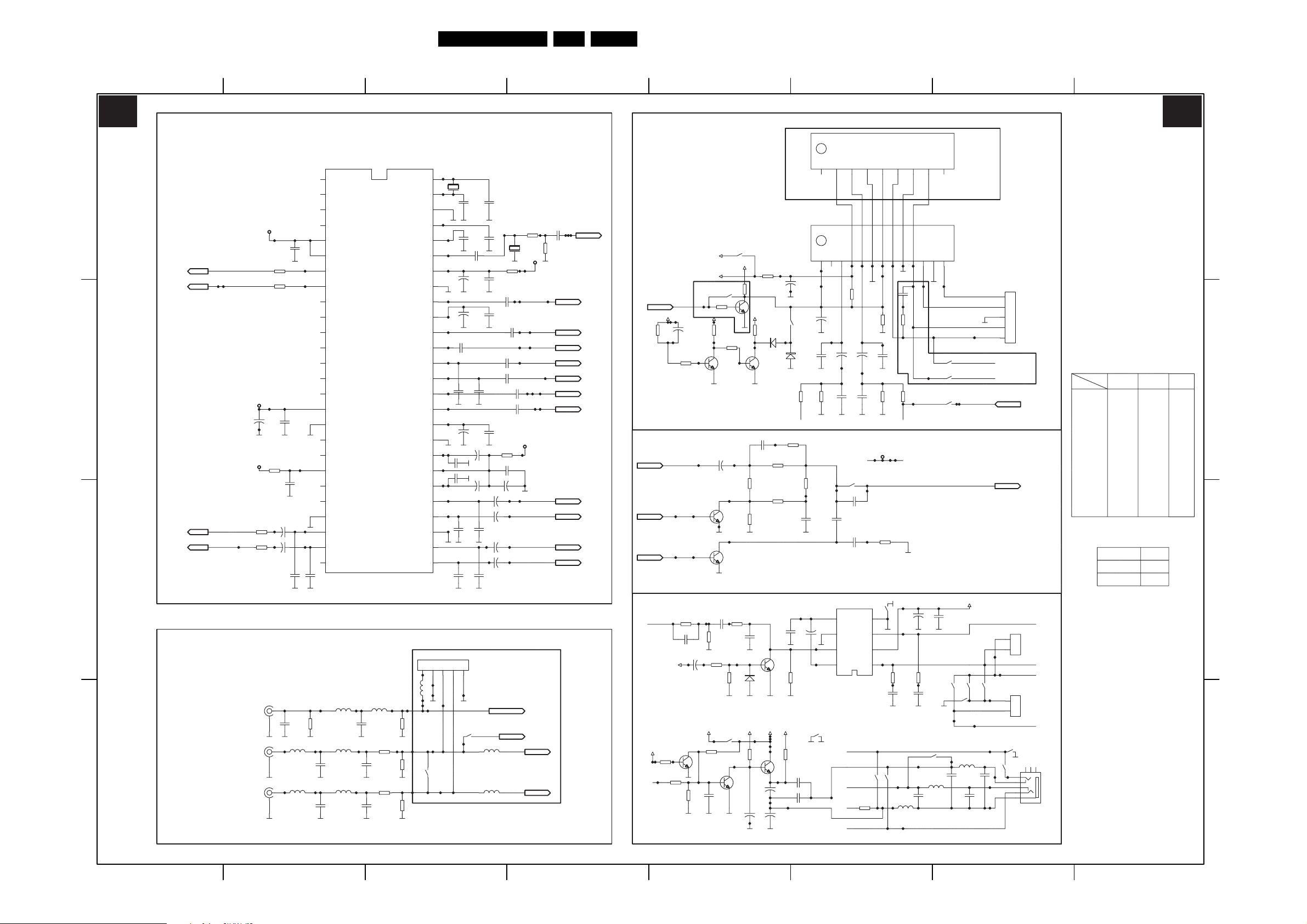
Circuit Diagrams and PWB Layouts
7. Circuit Diagrams and PWB Layouts
Main Panel (05TA085-5): MCU
EN 16TE3.2E CA 7.
7654321
8
A1 A1
MCU
D
5VD
5VD
J805
1
R201
D200
220R
J802
C201
100uF
R210
4.7K
C203
4N7
LED
J804
2
R202
220R
R206
1K5
J933
R212
R211
4.7K
4.7K
U200
3
VS
IR
1
OUT
J803
2
GND
TSOP34386
5VD
J807
J810
R203
C202
C200
47uF
J800
C
AV1/AV2
STDBY
B_OSD
G_OSD
R_OSD
FB_OSD
B
R200
220R
AV_ST.
L/L'
SDA
SCL
10uF
D201
2.7V
AV_ST.
L/L'
AV1/AV2
STDBY
B_OSD
G_OSD
R_OSD
FB_OSD
SDA
SCL
220R
R204
220R
J815
J814
J809
J830
J806
J831
J832
J833
J834
R207
4K7
5VD
5VA
R209
5.1K
C204
100nF
C208
10uF
J822
J821
J820
J813
R217
560R
R218
560R
R219
560R
R220
560R
T200
BC858
J816
5V
R213
4.7K
J817
C207
100uF
C205
100NF
5V
T201
BC848
LED
C209
22pF
R214
4.7K
R221
1K
R227
5.6k
R205
220R
C213
2.2nF
5VD
I201
R241
J202
OPT1
100R
R242
100R
5
SDA
6
SCL
7
PTC
8
VDD
5VD
C206
100nF
S200
1
2
BYEK -RI
3
4
5
S201
1
E
2
C
IV
3
R
ES
4
5
SERVICE
S202
3
RIAPMOC
2
1
COMPAIR
SDA
SDA
SCL
SCL
J201
OPT1
C217
470nF
C219
100pF
C212
22pF
C211
22pF
5VD
R230
C216
100N
2K2
5V
R208
4K7
5VA
T202
BC848
R216
4.7K
R231
220R
C223
10NF
5V 5V
R243
4K7
5V
J812
D202
LS4148
5V
R225
10K
R224
10K
R244
4K7
C225
470P
C220
100pF
R237
47K
J811
C222
R215
4.7K
R232
0R
R236
C224
1uF
C227
22uF
B200
C+
47K
R245
10K
R246
10K
R235
0R
*
R233
820R
R234
470R
12
SMART SOUND CONTROL
C218
470nF
D203
LS4148
J835
R238
560R
B201
C-
12
M-BASS
M-TREBLE
R226
J881
10K
C226
220PF
J880
CVBS_TXT
TXT-SW
V+
AV_ST2
TXT-SW
VOL
V_OSD
HOSD
1
B202
2
R240
18K
R239
1K5
D204
BAT85
AV_ST2
M-BASS
M-TREBLE
VOL
V_OSD
HOSD
CVBS_TXT
B203
V-
12
R222
10K
I200
1
P2.0/INT7
2
RESET
3
P0.7
4
P0.6
5
P0.5
6
P0.4
7
P0.3
8
P0.2/AIN4
9
P0.1
10
P0.0
11
P3.7/CSO
12
P3.6
13
P3.5
14
P3.4
15
BLUE
16
GREEN
17
RED
18
FB
19
SDA
20
SCL
21
VCC
22
JTDO
23
WSCF
24
WSCR
25
AVDD3
26
TEST
27
MCFM
28
JTCK
59129TS
P2.1/INT5/AIN1
P2.2/INT0/AIN2
P2.3/INT6/VS1
P2.4/NMI
P2.5/AIN3/VS2
OSCIN
OSCOUT
P4.7PWM7
P4.6
P4.5
P4.4
P4.3/PW3
P4.2
P4.1
P4.0
V_SYNC
H_SYNC
AVCC
PLLR
PLLF
VSS
AGND
CVBS1
CVBS2
JTMS
AVDD2
CVBS0
TXCF
KEYB
56
55
54
53
52
51
50
49
48
47
46
45
44
43
42
41
40
39
38
37
36
35
34
33
32
31
30
29
R229
15K
R223
5V
10K
J847
X200
4Mhz
C210
22pF
R228
5.6K
C215
4.7nF
5VA
C221
470N
C214
2.2nF
J801
J901
5VD
J900
5V
KEYB
J902
SDA
SCL
J823
4
VSS
3
A2
6
1
C42
2
A1
1
A0
IR
LED
KEYB
KEYB
J899
SCL
SCL
SDA
SDA
SDA
SCL
D
C
B
A
05TA085-5
A
G_16010_001.eps
190406
12345678
Page 17
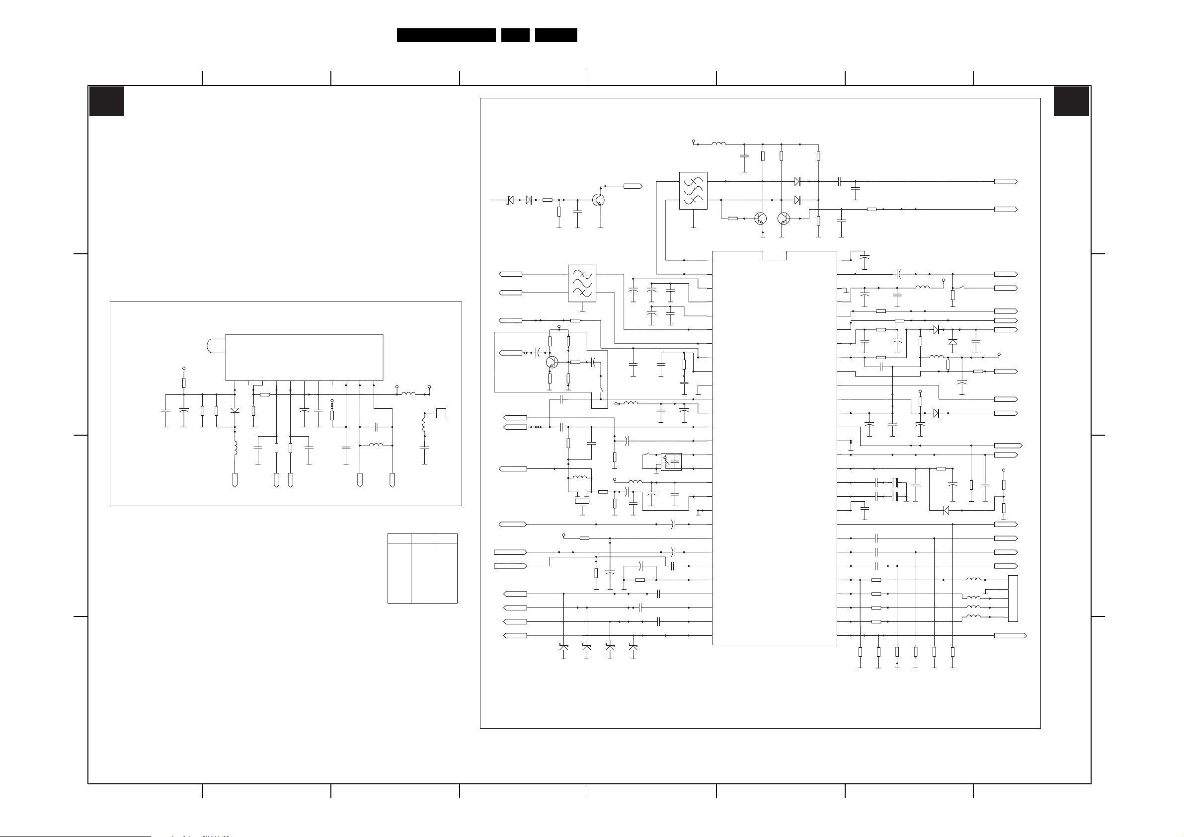
Circuit Diagrams and PWB Layouts
Main Panel (05TA085-5): Video
EN 17TE3.2E CA 7.
7654321
8
A2 A2
D
C
B
VIDEO
C300
100nF
TUNER
8V
L323
J878
10uH
F302
K9453
1
2
3
1
23
J919
R368
68K
I300
1
NC/SIF1
2
NC/SIF2
3
NC
4
VREF
5
AGCIF
6
PIFIN1
7
PIFIN2
8
AGCTU
9
IFPLL
10
GNDIF
11
FMOUT
12
VCCIF
13
CVBSOUT
14
EXTAUD
15
LC1
16
LC2
17
VCC2
18
CVBS1
19
GND
20
CVBS2
21
BS
22
CVBS3
23
CHR
24
APR
25
BEXT
26
GEXT
27
REXT
28
FBEXT
C359
1uF
C309
100nF
J306
0R
C361
1nF
C305
100nF
5
4
C354
C324
22nF
10uF
C355
C356
22nF
1uF
R362
150R
C363
330NF
C364
100uF
7
5
44MHz
L324
C306
C365
100nF
100uF
C358
1uF
C333
1uF
C307
100nF
C308
100nF
C310
100nF
J914
BCLG
J908
R313
1.2K
BCLG
T304
BC848
5
4
R322
N.U.
C332
1uF
C360
1nF
5V
L319
4.7uH
C367
*
8V
L320
C357
4.7uH
1uF
C339
22PF
C334
R364
1uF
330K
J917
J916
J915
D315
D314
5V1
5V1
D311
D303
ICATH
7.5V
IF1
IF2
AGC
T307 CTF5540
TUNER
1FHU/ADS
3F
N
FHU/SA
UT
H
U/LCS
/
NUT
4
3
R318
N.U.
R319
N.U.
R331
C326
100R
100pF
L
C
S
L
C
S
TFA/V5+
CN/V3
C
V5
N
/
+/
C
DA
C
N
5
7
6
8
9
33V
C301
100nF
C327
100pF
C302
100nF
J903
J877
R348
22K
C322
10uF
R332
100R
A
D
S
A
D
S
1F
2F
I
I
/
/
1FI
2F
3
I
+
0
1
2FI
2
F
I
C342
8.2pF
11
L317
1uH
5VT
1FI
1FI
C328
C367
C323
C325
J303 JUMPER
R357
R321
R311
R359
R349
T303
J305 JUMPER REM.
L314
10uH
C303
100nF
MONO STEREOCOMP.
22uF REM.
10uF
10uF
910R
10K
330R
2.4K
1K
BC848
L301
5V
J843
S302
1
CON1
F.B.
100PFREM.
REM
REM.
REM.
REM.
REM.
REM.
REM.
REM.
REM.
R329
27K
1
C
GA
CG
A/C
G
A
L306
12uH
C
G
A
D300
LS4148
2
5VT
R300
4K7
C319
R328
27K
47uF
LOUT1
SCART AUDIO OUT
MONO OPTION
EXT_AUD
SC
CVBS_OUT1
CVBS_EXT1
EXT2_IN
CHR
FBEXT
R356
10K
BAT85
IF1
IF2
AGC
LOUT1
J896
EXT_AUD
B
G
R
J898
C323
*
T303
*
J871
SC
J879
CVBS_OUT1
TRI.5.5/6.0/6.5MHZ
CVBS_EXT1
EXT2_IN
CHR
B
G
R
FBEXT
R357
*
R311
*
R337
C304
47K
100nF
F300
K3953M
1
2
3
R358
8V
680R
R321
*
C325
R349
*
*
R359
*
J303
R338
100R
D312
5V1
L318
4.7uH
*
C368
470pF
3
1
R312
1K
2
J913
R308
390K
R363
75R
D313
5V1
N.U.
J909
F301
C328
*
C351
8V
T305
BC848
C311
100nF
R323
10K
R324
10K
T306
BC848
84/6422VTS
D316
BA282
D317
BA282
R367
6.8K
R369
2.2K
FMCAP
AUDOUT
GND
VCC
SDA
SCL
SLPF
LFB/SSC
HOUT
VERT
BCL
VCC1
CVBSOUT1
GND1
VRMP
CLPF
XTAL1
XTAL2
XTAL3
FOSD
ROSD
GOSD
BOSD
ICATH
ROUT
GOUT
BOUT
NC/AGCSF
C362
1nF
IF1
OUT_L1
R353
470R
L/L'
SDA
SCL
HOSD
C329
100pF
VERT
BCLG
HOUT
ICATH
C374
N.U.
IF1
L/L'
AM_MONO
OUT_L1
SDA
SCL
HOSD
8V
HOUT
VERT
BCLG
CVBS_OUT2
V_AMP
5V
R365
330K
R366
330K
FB_OSD
R_OSD
G_OSD
B_OSD
S301
5
4
3
2
1
CON6
CVBS_TXT
C312
N.U.
R350
22K
C353
10nF
C335
56
1uF
55
54
C366
100uF
53
52
51
C370
50
4.7nF
49
C375
48
220PF
47
46
45
44
J945
43
42
41
C340
40
22pF
C341
39
0R
38
C315
100nF
37
36
C316 100nF
35
C317 100nF
34
C318 100nF
33
32
31
30
29
J918
R378
47K
J873
C336
1uF
R339
100R
R340
100R
R371
15K
C369
2.2uF
R370
2.2K
J904
C321
C314
47uF
100nF
J905
J906
X300
4.433619MHz
X301
3.579545MHz
R314
1K
R375
270R
R376
270R
R377
270R
R327
R3151KR3161KR3171KR379
10K
J808
C313
100nF
J907
L321
4.7uH
C371
4.7nF
V_AMP
D307
LS4148
R373
10K
R325
10K
J892
D305
LS4148
CVBS_OUT2
C337
1uF
5k6
AM_MONO
J305
*
J891
C372
10uF
R326
10K
FB_OSD
R_OSD
G_OSD
B_OSD
L302
F.B.
L303
F.B.
L304
F.B.
L305
F.B.
CVBS_TXT
J870
5V
J875
J876
D304
LS4148
R372
8.2K
L322
4.7uH
8V
R374
56K
D306
LS4148
C373
4.7uF
J897
R330
27K
D
C
B
A
05TA085-5
VIDEO & SOUND IF PROCESSING
A
G_16010_002.eps
190406
12345678
Page 18
Circuit Diagrams and PWB Layouts
Main Panel (05TA085-5): Sound
EN 18TE3.2E CA 7.
7654321
8
A3 A3
D
C
B
A
05TA085-5
SOUND
SCL
SDA
TV_S/R
TV_S/L
J930
TV_S/R
TV_S/L
SCL
SDA
K402
VIDEO
K403
L
K404
R
N.U.
5V
5V
R425
100R
R426
100R
J842
10uF
I402
*
1DN
P
.C.N
USV
NI
G
1C
V
R420
*
VOL1
C417
10uF
5
6
7
8
2
1
I
V
3PV4
R452
39K
C449
*
C451
*
C477
100NF
I404
IN-2
IN+2
IN+1
IN-1
TDA2822M
V
3
J414
C478
1uF
C453
10NF
HOUT+
OUT+
OUT1+
OUT-
HOUT1+
5
GND
OUT2
OUT1
R427
100R
2IV
C450
4.7UF
VS
0
24
J
5
4
DNGS
6
7
R418
4K7
C452
10NF
8V
R439
330R
4
3
2
1
.
U
.
N
I401
1
NC
2
AUD_OL_OUT
3
D_CTH_OUT1
4
C403
100nF
C421
1nF
10
11
12
13
14
15
16
17
18
19
20
21
22
23
24
25
26
C422
1nF
5
6
7
8
9
D_CTR_OUT0
ADA_SEL
STANDBYQ
I2C_CL
I2C_DA
I2S_CL
I2S_WS
I2S_DA_OUT
I2S_DA_IN1
ADA_DA
ADA_WS
ADA_CL
DVSUP
DVSS
I2S_DA_IN2
NC
RESETQ
DACA_R
DACA_L
VREF2
DACM_R
DACM_L
DACM_SUB
5V
J939
C401
100nF
R401
100R
R402
100R
C404
100nFC416
R409
47K
C442
1uF
C441
1uF
XTAL_OUT
G0143/G51
4
3PSM
SC1_OUT_L
SC1_OUT_R
SC2_OUT_L
SC2_OUT_R
XTAL_IN
TESTEN
ANA_IN2+
ANA_IN-
ANA_IN1+
AVSUP
AVSS
MONO_IN
VREFTOP
SC1_IN_R
SC1_IN_L
SC2_IN_R
SC2_IN_L
SC3_IN_R
SC3_IN_L
AGNDC
AHVSS
CAPL_M
AHVSUP
CAPL_A
VREF1
52
X401
18.432Mhz
51
C411
C412
2.2pF
C409
56pF
C408 56pF
C413
10uF
C437
3.3uF
C424
330nF
C431
100PF
C438
3.3uF
C414
10uF
C418
10uF
C433
100PF
C434
100PF
C432
100PF
C466
22uF
C467
22uF
C435
100PF
C468
22uF
C469
22uF
C436
100PF
2.2pF
C410
56pF
C402
100nF
C425
330nF
C406
100nF
C407
100nF
C405
100nF
C419
10uF
C426
330nF
R408
2.2R
R404
1R
C428
330nF
C427
330nF
R405
75R
X402
4.433619MHz
5V
J846
AM_MONO
J844
RIN1
J857
LIN1
J858
R2_IN
L2_IN
J864
C429
330nF
C430
330nF
J863
8V
J866
RIN2
LIN2
LOUT1
ROUT1
LOUT2
ROUT2
R406
220R
C415
220PF
AM_MONO
R2_IN
L2_IN
LOUT1
ROUT1
LOUT2
ROUT2
RIN1
LIN1
RIN2
LIN2
SC
SC
J845
VOL
OUT_L1
M-BASS
M-TREBLE
R411
100K
VOL
J855
R412
22K
OUT_L1
M-BASS
J850
M-TREBLE
J849
C439
100uF
T401
BC848
+12V-ST
J848
R413
T405
BC847B
T406
BC847B
VSUP
STEREO OPT.
16V6.5V
2K
J424
J859
C440
1uF
J937
R453
2K2
R415
1K2
R454
J401
3K3
+12V
16V
R435
2K7
R437
18K
T409
BC848
R414
2K
T402
BC848
33NF
R407
2.2R
D401
1N4148
C445
R416
3K9
R422
1K
50
49
48
47
46
45
44
43
42
41
40
39
38
37
36
35
1nF
34
C420
33
32
C423
1nF
31
30
29
28
27
I403
TDA7057QA
C446
1000uF/25V
J423
D402
1N4148
R403
100R
1
1CN2
J841
C447
*
R417
*
L/S_VT
R436
2K7
C455
100NF
STEREO SOUND PROCESSING
C473
C471
N.U.
+12V-ST
R455
N.U.
R429
N.U.
R430
N.U.
C457
100NF
680NF
R434
2K2
R431
N.U.
16V +12V VSUP
J412
T404
BC848
J943
C474
10NF
D403
N.U.
J416
R446
2K7
T408
BD135
C485
22uF
N.U.
J856
J839
T403
C443
2.2uF
C444
2.2uF
C475
22NF
R451
3K3
R447
0.22R FUSE
C458
100NF
C459
100NF
J826
J422
C476
47uF
R428
OUT_L
4K7
C470
2N2
5V
J413
VOL
R456
N.U.
R444
1K
8V
J837
T410
N.U.
R445
4K7
K401
J932
SIDE_AV
5
J872
FRONT_CVBS
J406
FAV_AUD
FRONT_CVBS
L411
FB
L412
FB
SIDE AV PART
FAV_AUD
L2_IN
R2_IN
L2_IN
R2_IN
1
234
L413
FB
J861
J852
J853
J854
J860
MONO
SIDE AV
50
OPTION
4
J
*
R450
N.U.
C481
220PF
C482
N.U.
L403
FB
L404
N.U.
L405
47uH
1
C479
2
10PF
L401
1
FB
2
L402
1
N.U.
2
C480
10PF
C483
10PF
C484
N.U.
L406
1uH
R448
0R
R449
N.U.
R441
N.U.
R443
N.U.
R442
N.U.
FRONT&SIDE AV OUT
2DNG
T
+T
-TU
NC
U
V
O
6
7
.C.N
O
9
8
4W MONO AMPLIFIER
2D
1DNGP
-2TUO01-1TUO
+
2TUO
2
N
C
GP
V
9
8
C454
4.7NF
R424
8R2
C448
100PF
R4211KR419
4K7
R
/S_VT
+1TUO
1
21
3
1
1
S401
5
4
3
2
1
CON5
J402
OUT-
OUT+
OUT_L
4W MONO OPT.
OUT_L
J403
J404
J838
4W MONO+2x3W STEREO AMPLIFIER
J874
OUT_L
OUT_L
MONO SMART SOUND
5
1
4J
C472
56uF
J825
R432
R433
4R7
4R7
C460
C461
100nF
100NF
J408
7
04
J
N.U.
L407
47uH
C462
100NF
L409
10uH
C456
100NF
VSUP
OUT+
S402
2
1
SPK ECO
HOUT1+
J828
114J
014J
904J
J421
S403
1
2
SPK ECO
HOUT+
J418
71
R
4
0
J
1
2
5
4
7
L410
10uH
C463
100NF
C464
100NF
J824
C465
100NF
1W MONO AMPLIFIER + HEADPHONE
OUT-
P401
FEATURE
4W 2X3W
COMP.
MONO STEREO
R453 2K2 REM.
R454 3K3 REM
T409 BC848 REM.
J424 REM. JUMPER
C454 4.7NF REM
R424 8R2 REM.
J402 JUMPER REM
J403 JUMPER REM
J404 JUMPER REM
I402 TDA7056B REM.
C447 REM 100PF
C449 REM. 4.7uF
REM.
C451 10NF
REM.
R420 1K
REM.
R417 4K7
R447 JUMPER 0.22R 1WREM.
C443 2.2uF REM 2.2uF
C444 2.2uF REM 2.2uF
R407 2.2K 1W REM. 100R
C458 100NF 100NF
C459 100NF 100NF
J401 REM.JUMPER REM.
J412 JUMPER JUMPER REM.
REM.
REM.
SPEAKERS
MONO 1W
MONO 4W
STEREO 2X3W
8
6
3
1x16R- 4W
1x8R- 5W
2x8R- 5W
G_16010_003.eps
12345678
1W
MONO
REM.
REM.
REM.
REM.
REM.
REM.
REM.
REM.
REM.
REM.
REM.
REM.
REM.
REM.
REM.
D
C
B
A
190406
Page 19
Circuit Diagrams and PWB Layouts
Main Panel (05TA085-5): Power
EN 19TE3.2E CA 7.
7654321
8
A4 A4
POWER
D
L102
FB.
R115
*
D111
BYV36C
*
R117
*
MODELS
L104
(SMT)
C119
C120
220pF
33N
C121
220P
L105
FB
R116
*
D108
*
D109
*
C124
*
R118
*
R119
*
14" MONO 21" STEREO21" MONO
SMT 21 PT19 MONO
ECO SMT SMT PT19 125V
!
L104
1
3
9
5
7
13
11
15
!
I101
6
6
5
5
4
4
*
I102 *
6
6
5
5
4
4
C125
R143
3.3M
1
1
2
2
3
3
!
1
1
2
2
3
3
4N7
R120
3.3M
!
L107
2
F.B.
D124
N.U.
L106
12
10
4
14
8
16
6
R128
D112
FB
BYV36C
D113
D125
*
R124
5A
D123
1N4007
6.5V
*
*
R129
*
D118
*
D119
D121
N.U.
*
T106
R133
*
DEGAUSSING SWITCHING CIRCUIT
D114
BYV36C
C136
100P
D117
Q100
C138
*
Z100
*
*
5VD
J938
R132
*
PART 2/2
HOT GROUND
COLD GROUND
*
*
*
J108
T103
BYW95C
D116
*
C140
*
J942
R105
*
C122
220P
R125
*
C127
2200uF
R130
R131
*
R121
15K
C129
2200uF
*
*
R134
*
C128
C137
C126
100nF
*
J884
C139
*
V101
*
R122
R123
15K
15K
R144
+12V
*
D104
N.U.
16V
C130
100nF
6.5V
J101
N.U.
C131
100nF
6.5V
R135
*
110Vi
R140
*
T104
J886
*
DEGAUSSING
SWITCHING CIRCUIT
100K
R101
BTB08/600V
T100
220R/1W
R119
MOC3041
I102
2K7
R133
2K7
R132
BC857
T103
4K7
R134
REMOVE
J109
STDBY
SYSTEM VOLTAGE :110Vdc FOR 14" CPT
D122
C141
22uF
ZTK338
STDBY
6.5V
J882
R137
J107
*
YBDTS
R126
*
J836
470R
J102
N.U.
+12V
110Vi
125Vdc FOR 21" CPT
C142
47uF/160V
J103
N.U.
R136
RF 0.5A
R138
0R
C143
10.5V
1
R139
1K8
8V
1
C132
100nF
T107
BD135
52
/
Fu74
I103
IN OUT
LM317
GND
I104
IN OUT
7805
GND
2
DNG
1uF/50
2
D110
D120
5V6
C145
L108
J925
5R6 5W
J887
L109
10uH
L110
C146
10uF/50
R127
22K
C144
100uF
10uH
STDBY
J862
C134
100nF
J883
C133
*
100nF
3
R141
330R
T105
R142
N.U.
BC848B
3
C135
100nF
J106
J865
STDBY
110VOUT
33V
5VD
5VA
5V
8V
5V
J111
!
F100
P100
S102
DEGAUSSE
L100
N.U.
J110
L101
N.U.
32
2
2
1
2.5A/250V
4
C
J105
!
S101
POWER CON
1
1
J104
C110
1nF
C104
V572Fn022
!
L103
2
1
LFP
T
I
U
CRIC GNIH
R101
2/1 TRAP
C
T
I
WS GNI
SS
UAGED
P101
PTH451A
1
!
*
R103
*
V572
4
Fn022
501C
R100
3
5R6 5W
J109
*
T100
23
C111
*
R104
*
R102
*
V100
*
C106
N.U.
C107
C108
C109
C100
2.2nF
D100
1N4007
D101
1N4007
C101
2.2nF
*
*
*
O100
N.U.
1
2
3
4
D105
*
I100
NC
PCS
RZI
SRC
ICE1QS01
R112
47K
R113
*
C118
N.U.
C102
2.2nF
D102
1N4007
D103
1N4007
C103
2.2nF
J818
J819
VCC
OUT
GND
OFC
R107
1M
100uF/400
C112
C113
R106
N.U.
C114
N.U.
8
7
R110
10R
6
5
R114
*
33uF
R108
390K
C117
C115
100N
C116
56P
LS4148
D107
N.U.
T101
*C123
J885
R109
1
47R
R111
10K
*
T102
D106
*
2
3
D115
*
B
14" CPT 21" CPT
C107
560PF 470PF
C109
6N8 3.3NF
C124
REM. 2.2uF
C128 10uF 470uF
C137
C138
C139 REM. 10NF
C140
D105
D106 T102
D108 REM. LS4148
D109 REM. LS4148
D110 0R LS4148
D113 REM. BYV36C
D115
D117
D118 REM. LS4148
D121 REM. 3.3V ZENER
4700uF
2200uF
REM.
22uF
REM.
100PF
REMOVELL4148
0R LL4148 REM. BC547
REM. 18V1
1N4007 BYW95C
14" CPT 21" CPT
D123 1N4007 REM.
D125 SS13 REM.
I101 REM. TCDT1101G
J107 JUMPER REM.
J108 JUMPER REM.
J416 REM. JUMPER
R102
2K2 18K
R103
REM. 1M
R104
REM. 0R
R105 REM. 4R7
R113
6K8 REMOVE
R114
2R2 100R
R115 68K 2W 33K 5W
R116 REM. 75R
R117 REM. 220R
R118
REM. 39K
R125
REM.
REM.
22K
22K
R126
14" CPT 21" CPTCOMP. COMP. COMP.
R128
REM. 820R
R129
REM. 1K
R130
R131
R135
R140
R144 FR 0,5A REM.
Q100
T101 04N60 9NC10NK
T104
T106 REM. BC848
V101
Z100
180K
REM.
REM.
2K7
REM.
4K7
REM.
130K
REM.
BC848
REM.
BC848
1KV100 REM.
REM. 20K
REM.
TL431
COMP.
D
C
B
A
05TA085-5
A
G_16010_004.eps
190406
12345678
Page 20
Circuit Diagrams and PWB Layouts
Main Panel (05TA085-5): Deflection
EN 20TE3.2E CA 7.
7654321
8
A5 A5
DEFLECTION
D
D604
BYV36C
R633
5.6K 3W
C622
EHT
FOCUS
G2
11
8
10
4
3
7
J940
4.7uF/250V
R634
1M
R639
2K
R640
2K
C613
100nF
C624
R632
0.22R
C623
*
D605
BYV36C
D607
BYV36C
D601
I600
N
TUO_FUB
EGP
THGIEH
MAA
D
NG
6
5
4
C602
47nF
R617
2K4
J922
C606
2200uF
R619
1K2
7
R614
8K2
R615
1K
R620
120R
C604
22uF
R621
1R
8
NI.VNI
R612
N.U.
SV
9
220NF
C600
0
1
J923
NE
G
.BF
C603
100uF
D600
1N4007
J941
24V
1
S600
VERT
TDA1771
NIGIAT
SVSO
TUO
1
2
3
J924
R607
2R2
C601
R609
220nF
220R
2
!
C
R600
V_AMP
V_OSD
VERT
V_AMP
VC
VC
V_OSD
J893
VERT
R605
R608
33K
**
R611
10K
T601
BC848
R613
1K5
100R
R606
10K
R604
T602
BC327
R603
180K
R602
150K
24V
3K3
T600
BC337
R610
220R
B
16V
HOUT
HOSD
+12V
J890
HOUT
006J
C611
100nF
D606
LS4148
HOSD
R622
10R
C607
47uF
C610
R625
47K
C609
10nF
22pF
R627
560R
C616
10N
R601
100R
T603
BC639
C615
2.2nF
2
HEATER
W600
L.DDRIVE
1
3
R624
75R
175V
TO-CRT
5
4
110VOUT
D602
BYV36C
1
2
3
4
S601
BYV36C
R623
0.22R
C608
REM.
C605
22uF/160V
R628
JUMPER
R629
39R
!
C620
10uF/250V
BU508DF
T604
D603
BYV36C
!
C617
*
R630
2R2/1W
*
R631
JUMPER
1
C618
*
2
5
9
6
HORZ
+B
VID
H
GND
FBT1
*
!
ABL
E/H
24V
12V
GND
100pF/1KV
L600
*
R616
1K
R6351MR636
R638
750K
C614
100nF
J601
*
C612
100nF
R643
10K
C621
1N2KV
1M5
R641
22K
C625
1000uF
L601
J602
*
*
R637
1M5
BCLG
J894
R642
R626
47K
J934
J935
J936
BCLG
R618
S602
1
!
2
HDY
VC
8V
J895
*
24V
J944
33V
D
C
B
A
05TA085-5
VERTICAL
CPT
14" EKRANAS 21" SAMSUNG TF21" EKRANAS TF 21" LG-PHILIPS
A33EKC02X01 A51EKS71X11 A51QDJ420X05
COMP. A51QDX993X230
6.2NF 1.6KV
C618
470PF 2KV
C617
470NF 250V
C623
L601
J601
J602
L600
R631
R618
FBT1 14" FBT 14" FBT 21" FBT 21" FBT 21" FBT
---
---
JUMPER
LINEARITY 100uH
JUMPER
3.9K
HORIZONTAL
14" LG-PHILIPS
A34EAK02X31
6.2NF 1.6KV
470PF 2KV
470NF 250V
COIL 56uH
LINEARITY 100uH
JUMPER
---
---
3.3K
7.2NF 1.6KV
---
270NF 250V
---
---
JUMPER
LINEARITY 100uH
JUMPER
3.9K
6.8NF 1.6KV
220PF 2KV
240NF 250V
---
---
JUMPER
LINEARITY 150uH
JUMPER
3.3K
6.8NF 1.6KV
--280NF 250V
COIL 56uH
---
---
LINEARITY 200uH
JUMPER
3.3K
A
G_16010_005.eps
190406
12345678
Page 21

CRT Panel (05TA085-5)
Circuit Diagrams and PWB Layouts
EN 21TE3.2E CA 7.
7654321
8
D
C
B
A6
CRT
S501
CON5
A6
D
D510
22PF
D501
BAV21
D502
BAV21
D503
BAV21
S502
JUMPER
!
S506
R517
1K5
R518
1K5
R519
1K5
RED
GRN
BLU
6
RED
8
GREEN
3
BLUE
*
C
1
D
NG
1G
2
F
2
4
9
1G
2G
73G1
2G
2
D
N
G
5
!
C516
R522
1K5
D506
1N4007
R530
1K5
1N2KV
S505
1
CON1
S507
1
CON1
C509
**
GND2
B
!
R533
*
!
R520
150K
C508
C504
**
47N630V
1
2
4
3
CON4
R
HTRAE
V571+
ETAEH
C505
2.2U250V
R521
2M2
R513
R510
27K 2W
J927
GND2
GND2
GND2
R501
820R
R502
820R
R503
820R
T501
BF422
C501
330PF
T502
BF422
C502
330PF
T503
BF422
C503
330PF
R504
510R
R505
10R
R506
510R
R507
10R
R508
510R
R509
10R
BAT85
27K 2W
J928
R512
27K 2W
J926
D504
R511
GND2
R525
J929
0R
R527
0R
R529
0R
GND2
3
5
1
2
4
N
HTACI
E
E
ERG
DER
U
L
B
220R
T504
BF422
R514
!
220R
T506
BF422
!
R515
220R
T508
BF422
D505
BZX55C 8.2V
T505
BF423
T507
BF423
T509
BF423
GND2
!
R516
5K6 1W
C507
A
05TA085-5
CPT
14" EKRANAS 21" SAMSUNG TF21" EKRANAS TF 21" LG-PHILIPS
A33EKC02X01 A51EKS71X11 A51QDJ420X05
COMP. A51QDX993X230
R533
S506 MINI NECKNARROW NECK NARROW NECK NARROW NECK NARROW NECK
14" LG-PHILIPS
A34EAK02X31
0.68R 1W 0.22R 1W 2.7R 1W
1.5R 1W 2.2R 1W
A
G_16010_006.eps
190406
12345678
Page 22
Circuit Diagrams and PWB Layouts
Main Panel (05TA085-5): SCART
EN 22TE3.2E CA 7.
7654321
8
A7 A7
D
C
SCART
8V
R761
R725
75R
R730
100R
12K
N.U.
R763
2K2
J701
R726
75R
J705
C708
N.U.
C709
N.U.
C710
N.U
C711
N.U.
R731
100R
L707
12uH
L709
12uH
R703
R704
R762
4K7
T710
BC848
R764
680R
*
*
R727
150R
R732
100R
J867
J888
EXT_AUDFAV_AUD
MONO APPLICATIONS
LIN1
R715
*
C712
330PF
C713
330PF
R717
*
C714
330PF
C715
330PF
R735
8K2
R748
R765
N.U.
150R
C701
AV1/AV2
J889
R701
3K3
R708
10K
1uF
FAV_AUD EXT_AUD
AV1/AV2
MONO+FAV APPLICATIONS
MONO+SIDE AV APPLICATIONS
S701
SCART1
1
2
3
4
5
6
7
9
11
13
15
17
19
21
J829 J851
8
10
12
14
16
18
20
L711
F.B.
R720
75R
C703
47uF
R741
1K
5V
T703
BC848
R729
22R
R702
10K
L713
JUMPER
8V
R733
100R
R711
8K2
BC848
T701
J911
R758
6K8
R712
3.3K
D701
LS4148
J920
R723
75R
8V
R713
8K2
T702
BC848
C726
22PF
R759
6K8
D702
*
R766
*
L701
F.B
J702
MONO OPS.
L703
F.B
L704
F.B
L715
FB
D704
5.1V
C702
1uF
R724
75R
L717
10uH
10uH
R760
10R
L718
ROUT1
RIN1
LOUT1
J703
MONO OPS.
LIN1
B
G
R
FBEXT
AV_ST.
CVBS_EXT1
CVBS_OUT1
LIN1
ROUT1
RIN1
LOUT1
LIN1
B
G
R
FBEXT
AV_ST.
CVBS_EXT1
CVBS_OUT1
J921
S702
SCART2
1
3
5
7
9
11
13
15
17
19
21
L702
F.B
2
4
6
8
10
12
14
16
18
20
L712
F.B.
R721
75R
T704
BC848
R742
1K
C724
10uF
L714
JUMPER
8V
R736
22R
J910
R705
12K
R734
100R
J706
C704
47uF
R756
75R
L705
F.B
L706
F.B
L716
FB
L719
12uH
5V
D703
LS4148
R714
4K7
12uH
L720
R722
75R
C716
N.U.
C717
N.U.
C718
N.U.
C719
N.U.
L708
12uH
L710
12uH
R706
12K
R707
12K
R757
100R
J869
J868
R716
470R
C720
330PF
C721
330PF
R718
470R
C722
330PF
C723
330PF
C725
22PF
ROUT2
RIN2
LOUT2
LIN2
AV_ST2
CHR
CVBS_EXT2IN
CVBS_OUT2
ROUT2
RIN2
LOUT2
LIN2
AV_ST2
CHR
CVBS_EXT2IN
CVBS_OUT2
D
C
B
A
05TA085-5
FEATURES
COMPONENT
D702
R766
R703
R704
R717
R715 REM. REM.
WITH FAV WITHOUT FAV
OR OR
WITH SIDE AV WITHOUT SIDE AV
LS4148 0R
5K6 REM.
3K3 8K2
3K3 8K2
22R 22R
SCART1
STEREO
MODELS
REM.
REM.
10K
10K
470R
470R
CVBS_EXT2IN
EXT2_IN
CVBS_EXT2IN
EXT2_IN
R744
1K
SWITCH CIRCUIT FOR DOUBLE SCART AND SIDE AV APPLICATIONS
R752
R745
1K
T706
BC848
C705
47uF
R746
1K
22K
R709
10K
T707
BC848
J704
1SCART OPT.
T708
BC848
C706
47uF
R747
1K
R755
47K
R710
10K
SCART2
R737
4R7
R753
C707
22K
47uF
R719
0R
R754
22K
T709
BC848
B
8V
FRONT_CVBS
FRONT_CVBS
J912
AV1/AV2
AV1/AV2
R728
C727
75R
1N
A
G_16010_007.eps
190406
12345678
Page 23
Circuit Diagrams and PWB Layouts
Layout Main Panel (05TA085-5) (Top Side)
EN 23TE3.2E CA 7.
05TA085-5
G_16010_008.eps
190406
Page 24
Circuit Diagrams and PWB Layouts
Layout Main Panel (05TA085-5) (Bottom Side)
EN 24TE3.2E CA 7.
05TA085-5
G_16010_009.eps
190406
Page 25

Circuit Diagrams and PWB Layouts
Main Panel (05TA085-6): MCU
EN 25TE3.2E CA 7.
7654321
8
MCU
A1 A1
D
5VD
R247
C204
100nF
C208
10uF
J822
J821
J820
J813
R217
560R
R218
560R
R219
560R
R220
560R
J816
IR
T200
BC858
5VM
5K6
J803
C207
100uF
C205
100NF
U200
2
VS
1
OUT
3
GND
TSOP2236
5VD
J807
J810
R203
C202
C200
47uF
J800
C
AV_ST.
AV1/AV2
STDBY
B_OSD
G_OSD
R_OSD
FB_OSD
B
SDA
220R
10uF
D201
2.7V
R204
220R
AV_ST.
L/L'
AV1/AV2
STDBY
B_OSD
G_OSD
R_OSD
FB_OSD
SDA
SCL
J815
J814
J809
J830
J806
J831
J832
J833
J834
R207
4K7
R209
5VD
5VA
5.1K
R200
220R
L/L'
SCL
J817
R213
4.7K
J802
R201
220R
C201
220uF
R210
4.7K
C203
4N7
J805
12
D200
LED
J804
R202
220R
R206
1K5
J933
5VM
R212
R211
4.7K
4.7K
5VD
5VD
T201
BC848
LED
C209
22pF
R221
1K
R214
4.7K
R205
0R
R227
5.6k
C213
2.2nF
5VD
I201
R241
J202
OPT1
100R
R242
100R
5
SDA
6
SCL
7
PTC
8
VDD
5VD
C206
100nF
5VD
S20 0
1
2
3
4
IR- KEYB
5
S201
1
J801
2
3
SERVICE
4
5
SERV CE
S20 2
3
J901
2
1
COMPAIR
COMPAIR
SDA
SDA
C217
470nF
C219
100pF
C212
22pF
C211
22pF
5VD
R230
2K2
C216
100N
5VM
R208
4K7
5VA
R216
4.7K
C223
10NF
5VM 5VM
R243
4K7
5VM
5VM
R225
10K
T202
BC848
J812
D202
LS4148
R231
220R
R224
10K
R244
4K7
C225
470P
C220
100pF
R237
47K
J811
C222
R232
0R
R215
4.7K
R236
C224
1uF
C227
22uF
B200
C+
47K
*
R233
820R
R234
470R
1 2
SMART SOUND CONTROL
R245
10K
R246
10K
R235
0R
R226
C218
470nF
10K
C226
220PF
D203
LS4148
J835
1 2
R238
560R
B201
C-
M-BASS
M-TREBLE
J881
J880
CVBS_TXT
TXT-SW
V+
AV_ST2
TXT-SW
VOL
V_OSD
HOSD
12
R240
18K
R239
1K5
B202
D204
BAT85
AV_ST2
M-BASS
M-TREBLE
VOL
V_OSD
HOSD
CVBS_TXT
B203
V-
1 2
R222
10K
I200
1
P2.0/INT7
2
RESET
3
P0.7
4
P0.6
5
P0.5
6
P0.4
7
P0.3
8
P0.2/AIN4
9
P0.1
10
P0.0
11
P3.7/CSO
12
P3.6
13
P3.5
14
P3.4
15
BLUE
16
GREEN
17
RED
18
FB
19
SDA
20
SCL
21
VCC
22
JTDO
23
WSCF
24
WSCR
25
AVDD3
26
TEST
27
MCFM
28
JTCK
P2.1/INT5/AIN1
P2.2/INT0/AIN2
P2.3/INT6/VS1
P2.5/AIN3/VS2
ST92195
P2.4/NM I
OSCIN
OSCOUT
P4.7PWM7
P4.3/PW3
V_SYNC
H_SYNC
AVCC
PLLR
PLLF
AGND
CVBS1
CVBS2
JTMS
AVDD2
CVBS0
TXCF
P4.6
P4.5
P4.4
P4.2
P4.1
P4.0
VSS
56
55
54
53
52
51
50
49
48
47
46
45
44
43
42
41
40
39
38
37
36
35
34
33
32
31
30
29
R229
15K
R223
10K
KEYB
5VM
X200
4Mhz
C210
22pF
R228
5.6K
C215
4.7nF
5VA
C221
470N
C214
2.2nF
SCL
SCL
J201
OPT1
5V
J900
LED
KEYB
J823
J902
SDA
SCL
VSS
A2
A1
24C16
A0
IR
KEYB
J899
SCL
SDA
SDA
SCL
4
3
2
1
KEYB
SCL
SDA
D
C
B
A
05TA085-6
A
G_16010_029.eps
190406
1 2 3 4 5 6 78
Page 26

Circuit Diagrams and PWB Layouts
Main Panel (05TA085-6): Video
EN 26TE3.2E CA 7.
7654321
8
A2 A2
VIDEO
8V
L323
J878
10uH
D
J306
0R
C359
1uF
C309
100nF
C361
1nF
C305
100nF
5
4
C354
C324
22nF
10uF
C355
C356
22nF
1uF
R362
150R
C363
330NF
C364
100uF
7
5
L324
C365
100uF
C358
1uF
C333
1uF
C307
100nF
C308
100nF
C310
100nF
J914
BCLG
J908
5
4
R313
1.2K
R322
N.U.
T304
BC848
5V
8V
C334
1uF
D314
5V1
C360
1nF
C339
22PF
C367
*
C357
1uF
L319
4.7uH
J917
J916
J915
BCLG
L320
R364
330K
C332
1uF
4.7uH
D315
5V1
D311
D303
ICATH
7.5V
IF1
IF2
AGC
T307 CTF5540
R318
N.U.
C326
100pF
SCL
R331
100R
SCL
TUNER
C322
10uF
100nF
R332
100R
SDA
SDA
C301
C327
100pF
33V
J903
J877
R348
22K
C302
100nF
LOUT1
SCART AUDIO OUT
MONO OPTION
EXT_AUD
SC
CVBS_OUT1
CVBS_EXT1
EXT2_IN
CHR
FBEXT
L314
10uH
C303
100nF
MONO STEREOCOMP.
22uF REM.
10uF
10uF
910R
10K
330R
2.4K
1K
BC848
L301
5V
J843
S302
1
CON1
F.B.
100PFREM.
REM
REM.
REM.
REM.
REM.
REM.
REM.
REM.
REM.
5VT
11
C342
8.2pF
L317
1uH
IF2
IF2
IF1
IF1
C328
C367
C323
C325
J303 JUMPER
R357
R321
R311
R359
R349
T303
J305 JUMPER REM.
C
5VT
R300
4K7
C300
C319
47uF
100nF
TUNER
R328
27K
AGC/AGC1TUN/TUN2AS/UHF3SCL/UHF34SDA/UHF15NC/+5V6+5V/AFT7ADC/NC8+33V/NC9IF2/IF210IF1/IF1
D300
R329
27K
AGC
AGC
L306
12uH
LS4148
R319
N.U.
B
R356
10K
BAT85
IF1
IF2
AGC
LOUT1
J896
EXT_AUD
B
G
R
J898
C323
*
T303
*
SC
J871
J879
CVBS_OUT1
CVBS_EXT1
EXT2_IN
CHR
B
G
R
FBEXT
R337
47K
F300
K3953M
1
2
R358
8V
680R
R321
R357
*
*
R349
*
R359
R311
*
*
C328
*
C351
N.U.
R338
100R
F301
TRI.5.5/6.0/6.5MHZ
8V
J909
D312
5V1
L318
4.7uH
123
R308
390K
C304
100nF
J950
3
C325
*
D313
5V1
J303
*
C368
470pF
J913
R312
1K
R363
75R
44MHz
C306
100nF
F302
K9453
1
2
3
J951
1
23
J919
R368
68K
I300
1
NC/SIF1
2
NC/SIF2
3
NC
4
VREF
5
AGCIF
6
PIFIN1
7
PIFIN2
8
AGCTU
9
IFPLL
10
GNDIF
11
FMOUT
12
VCCIF
13
CVBSOUT
14
EXTAUD
15
LC1
16
LC2
17
VCC2
18
CVBS1
19
GND
20
CVBS2
21
BS
22
CVBS3
23
CHR
24
APR
25
BEXT
26
GEXT
27
REXT
28
FBEXT
T305
BC848
C311
100nF
R323
R324
10K
10K
J947
STV2246/48
T306
BC848
D316
BA282
D317
BA282
R367
6.8K
R369
2.2K
FMCAP
AUDOUT
GND
VCC
SDA
SCL
SLPF
LFB/SSC
HOUT
VERT
BCL
VCC1
CVBSOUT1
GND1
VRMP
CLPF
XTAL1
XTAL2
XTAL3
FOSD
ROSD
GOSD
BOSD
ICATH
ROUT
GOUT
BOUT
NC/AGCSF
C362
1nF
C312
N.U.
R350
22K
C353
10nF
C335
56
1uF
55
54
C366
100uF
53
52
51
C370
50
4.7nF
49
C375
48
220PF
47
46
45
44
J945
43
42
41
C340
40
22pF
C341
39
0R
38
C315
100nF
37
36
C316 100nF
35
C317 100nF
34
C318 100nF
33
32
31
30
J918
29
R378
47K
C336
1uF
R339
100R
R340
100R
R371
15K
C369
2.2uF
R370
2.2K
J904
C321
C314
47uF
100nF
J905
J906
X300
4.433619MHz
X301
3.579545MHz
R314
1K
R375
270R
R376
270R
R377
270R
R3151KR3161KR3171KR379
R327
10K
J808
J873
C313
100nF
J907
L321
4.7uH
8V
C371
4.7nF
R372
8.2K
R374
56K
J875
J876
C373
4.7uF
J870
L322
4.7uH
D304
LS4148
D306
LS4148
J897
R330
27K
5V
V_AMP
D307
LS4148
R373
10K
R325
10K
5k6
J892
D305
LS4148
C337
1uF
AM_MONO
J305
OUT_L1
*
J891
R353
470R
C372
10uF
CVBS_OUT2
R326
10K
FB_OSD
R_OSD
G_OSD
B_OSD
L302
F.B.
L303
F.B.
L304
F.B.
L305
F.B.
CVBS_TXT
IF1
L/L'
SDA
SCL
HOSD
C329
100pF
VERT
BCLG
HOUT
ICATH
AM_MONO
OUT_L1
8V
HOUT
CVBS_OUT2
V_AMP
C374
N.U.
FB_OSD
R_OSD
G_OSD
B_OSD
5
4
3
2
1
IF1
L/L'
SDA
SCL
HOSD
VERT
BCLG
5V
R365
330K
R366
330K
S301
CON6
CVBS_TXT
A2
D
C
B
A
05TA085-6
A5
1
VIDEO & SOUND IF PROCESSING
L325
F.B.
A
G_16010_030.eps
190406
1 2 3 4 5 6 78
Page 27

Circuit Diagrams and PWB Layouts
Main Panel (05TA085-6): Sound
EN 27TE3.2E CA 7.
7654321
8
A3 A3
SOUND
I402
*
D
C
B
A
05TA085-6
I401
SCL
SDA
TV_S/R
TV_S/L
J930
TV_S/R
TV_S/L
SCL
SDA
5V
5V
R425
100R
R426
100R
J842
10uF
1
NC
2
AUD_OL_OUT
3
D_CTH_OUT1
4
C403
100nF
C421
1nF
10
11
12
13
14
15
16
17
18
19
20
21
22
23
24
25
26
C422
1nF
5
6
7
8
9
D_CTR_OUT0
ADA_SEL
STANDBYQ
I2C_CL
I2C_DA
I2S_CL
I2S_WS
I2S_DA_OUT
I2S_DA_IN1
ADA_DA
ADA_WS
ADA_CL
DVSUP
DVSS
I2S_DA_IN2
NC
RESETQ
DACA_R
DACA_L
VREF2
DACM_R
DACM_L
DACM_SUB
5V
J939
C401
100nF
R401
100R
R402
100R
C404
100nFC416
R409
47K
C442
1uF
C441
1uF
XTAL_OUT
MSP3415G/3410G
SC1_OUT_L
SC1_OUT_R
SC2_OUT_L
SC2_OUT_R
XTAL_IN
TESTEN
ANA_IN2+
ANA_IN-
ANA_IN1+
AVSUP
AVSS
MONO_IN
VREFTOP
SC1_IN_R
SC1_IN_L
SC2_IN_R
SC2_IN_L
SC3_IN_R
SC3_IN_L
AGNDC
AHVSS
CAPL_M
AHVSUP
CAPL_A
VREF1
52
X401
18.432Mhz
51
C411
C412
2.2pF
C409
56pF
C408 56pF
C413
10uF
C437
3.3uF
C424
330nF
C431
100PF
C438
3.3uF
C414
10uF
C418
10uF
C433
100PF
C434
100PF
C432
100PF
C466
22uF
C467
22uF
C435
100PF
C468
22uF
C469
22uF
C436
100PF
2.2pF
C410
56pF
C402
100nF
C425
330nF
C406
100nF
C407
100nF
C405
100nF
C419
10uF
C426
330nF
R408
2.2R
R404
1R
C428
330nF
C427
330nF
R405
75R
X402
4.433619MHz
5V
J846
AM_MONO
J844
RIN1
J857
LIN 1
J858
R2_IN
L2_IN
J864
C429
330nF
C430
330nF
8V
J866
J863
LOUT1
ROUT1
LOUT2
ROUT2
RIN2
LIN 2
R406
220R
C415
220PF
AM_MONO
R2_IN
L2_IN
LOUT1
ROUT1
LOUT2
ROUT2
RIN1
LIN 1
RIN2
LIN 2
R407
2.2R
R414
2K
TV_S/L
R457
T402
BC848
*
5V
D401
1N4148
R435
2K7
R437
18K
R417
*
33NF
TDA7057QA
R458
10K
C445
SC
SC
J845
VSUP
J401
+12V
+12V-ST
R454
*
J424
VOL
R411
100K
M-TREBLE
OUT_L1
M-BASS
J855
VOL
R412
22K
C439
100uF
OUT_L1
M-BASS
M-TREBLE
T401
BC848
J849
J850
J848
R413
16V6.5V
2K
STEREO OPT.
J859
R453
2K2
T405
BC847B
T406
BC847B
R415
1K2
C440
1uF
J937
T409
BC848
16V
50
49
48
47
46
45
44
43
42
41
40
39
38
37
36
35
1nF
34
C420
33
32
C423
1nF
31
30
29
28
27
STEREO SOUND PROCESSING
C473
C471
N.U.
+12V-ST
R455
N.U.
R429
N.U.
R430
N.U.
C457
100NF
680NF
R434
2K2
R431
N.U.
16V +12V VSUP
J412
T404
BC848
J943
C474
10NF
D403
N.U.
J416
R446
2K7
T408
BD135
C485
22uF
J856
J839
T403
N.U.
R447
0.22R FUSE
J425
C443
2.2uF
J826
C444
2.2uF
K402
VIDEO
K403
L
K404
R
N.U.
R428
OUT_L
4K7
C470
2N2
5V
J413
VOL
R456
N.U.
8V
R444
1K
J837
T410
N.U.
R445
4K7
K401
J932
SIDE_AV
J872
FRONT_CVBS
J406
FAV_AUD
FRONT_CVBS
L411
FB
L412
FB
SIDE AV PART
FAV_AUD
L2_IN
R2_IN
L2_IN
R2_IN
12345
L413
FB
J861
J852
J853
J854
J405
J860
MONO
SIDE AV
OPTION
*
R450
N.U.
C481
220PF
C482
N.U.
L403
FB
L404
N.U.
L405
47uH
1
C479
2
10PF
L401
1
FB
2
L402
1
N.U.
2
C480
10PF
C483
10PF
C484
N.U.
L406
1uH
R448
0R
R449
N.U.
R441
N.U.
R443
N.U.
R442
N.U.
FRONT&SIDE AV OUT
1 2 3 4 5 6 78
N.C.1VSUP2VIN
3
I403
VCNT5OUT+6GND27OUT-8N.C.
GND1
4
VC11NC2VI13VP4VI25SGND6VC27OUT2+8PGND29OUT2-10OUT1-11PGND112OUT1+
J841
C446
1000uF/25V
R452
*
VOL1
C449
*
C451*C452
I404
IN-2
IN+2
IN+1
IN-1
TDA2822M
10NF
GND
OUT2
OUT1
C450
4.7UF
R461
390R
C477
100NF
VS
R418
4K7
J414
C478
1uF
C453
10NF
R463
1K
4
3
2
1
D405
LS4148
T412
BC848
J415
J948
J423
1N4148
R416
3K9
R422
1K
C475
22NF
R451
3K3
D402
5V
R420
*
D404
LS4148
T411
BC848
R403
100R
J422
C476
47uF
C447
*
C417
10uF
5
6
7
8
R459
390R
R460
1K
R436
2K7
C455
100NF
HOUT+
OUT+
C458
100NF
C459
100NF
OUT-
OUT1+
R427
100R
J420
J407
N.U.
HOUT1+
9
4W MONO AM PLIFIER
13
C448
100PF
C454
4.7NF
R424
8R2
J402
5V
R462
10K
R419
10K
R421
8K2
OUT-
J403
OUT+
J404
TV_S/R
J838
5
4
3
2
1
4W MONO OPT.
OUT_L
S401
CON5
OUT_L
4W MONO+2x3W STEREO AMPLI FIER
8V
J874
OUT_L
OUT_L
R439
330R
MONO SMART SOUND
VSUP
C472
C456
56uF
100NF
J825
OUT+
S402
2
1
SPK ECO
OUT-
HOUT1+
J411
J828
S403
1
R432
4R7
C460
100nF
R433
4R7
C461
100NF
J409
J421
J410
2
SPK ECO
J417
J418
0R
1
2
5
4
7
HOUT+
P401
J824
J408
N.U.
C462
100NF
L407
47uH
L409
10uH
L410
10uH
C463
100NF
C464
100NF
C465
100NF
1W MONO AMPLIFIER + HEADPHONE
FEATURE
4W 2X3W
COMP.
MONO STEREO
C443 2.2uF REM 2.2uF
C444 2.2uF REM 2.2uF
C447 REM 100PF
C449 REM. 4.7uF
C451 10NF
REM.
C454 4.7NF REM
C458 100NF 100NF
C459 100NF 100NF
I402 TDA7056B REM.
J401 REM.JUMPER REM.
J402 JUMPER REM
J403 JUMPER REM
J404 JUMPER REM
J412 JUMPER JUMPER REM.
J424 REM. JUMPER
R407 2.2K 1W REM. 100R
R417 10K
R420 8K2
R424 8R2 REM .
R447 JUMPER 0.22R 1WREM.
R453 2K 2 REM.
R452 REM REM REM.
R454 REM REM
R457 3.3K REM. REM.
T409 BC848 REM.
REM.
REM.
REM.
REM.
SPEAKERS
MONO 1W
MONO 4W
STEREO 2X3W
638
1x16R- 4W
1x8R- 5W
2x8R- 5W
G_16010_031.eps
1W
MONO
REM.
REM.
REM.
REM.
REM.
REM.
REM.
REM.
REM.
REM.
REM.
REM.
REM.
REM.
REM.
190406
D
C
B
A
Page 28

Circuit Diagrams and PWB Layouts
Main Panel (05TA085-6): Power
EN 28TE3.2E CA 7.
7654321
8
A4 A4
POWER
D
!
R107
1M
100uF/400
C112
C113
R106
N.U.
C114
N.U.
8
7
R110
10R
6
5
R114
*
33uF
R108
C117
390K
C115
100N
C116
56P
D107
LS4148
N.U.
R109
47R
R111
10K
*
T102
D106
T101
J885
1
*
23
*
*
R117
D115
*
!
F100
T2.5AL 250V
!
32
4
P100
C
J105
!
!
S101
POWER CON
1
1
!
2
S102
DEGAUSSE
R143
3.3M
R120
3.3M
2
1
L103
2
C104
1
R145
220R 1/2W
220nF275V
J104
!
DEGAUSSING SWITCHING
P101
C110
1nF
PTH451A
!
LFP
4
C105
220nF275V
R100
3
R146
DSP
*
R101
*
T100
PART 1/2
CIRCUIT
1
!
R103
*
5R6 5W
J109
23
C111
*
R104
*
R102
*
V100
*
C106
N.U.
C107
C109
*
C108
*
*
O100
N.U.
C100
2.2nF
D100
1N5062
D101
1N5062
C101
2.2nF
*
1
2
3
4
D105
I100
C102
2.2nF
J818
D102
1N5062
D103
J819
1N5062
C103
2.2nF
NC
PCS
RZI
SRC
C118
N.U.
ICE1QS01
R112
47K
R113
*
VCC
OUT
GND
OFC
!
B
14" CPT 21" CPT
C107
560PF 470PF
C109
6N8 3.3NF
C124
REM. 2.2uF
C128 10uF 470uF
C137 R10 2
C138
C139 REM. 10NF
C140
D108 REM. LS4148
D109 REM. LS4148
D110 0R LS4148
D113 BYW95C BYV36C
D115
D117
D118 REM. LS4148
D121 REM. 3.3V ZENER
4700uF
2200uF
REM.
22uF
REM.
100PF
REM. 18V1
BYW95C BYW95C
14" CPT 21" CPT
D123 BYW95C REM.
I101 REM. TCDT1101G
J107 JUMPER REM.
J416 RE M. JUMPER
2K2 18K
R103
REM. 1M
R104
REM. 0R
R105 REM. 4R7
R113D105
6K8 REMOVEREMOVELL4148
R114D106
2R2 100R0R LL4148
R115 68K 2W 33K 5W
R116 REM. 75R
R117 REM. 220R
R118
REM. 39K
REM.
R125
R126
R128
R129
22K
REM.
22K
REM. 820R
REM. 1K
14" CPT 21" CPTCOMP. COMP. COMP.
R130
R131
R135
R140
R144 FR 0,5A REM.
Q100
T101 05N60 9NC10NK
T102
T104
T106 REM. BC848
V101
Z100
180K
REM.
REM.
2K7
REM.
4K7
REM.
130K
REM.
BC848
REM. BC547
REM.
BC848
1KV100 REM.
REM. 20K
REM.
TL431
COMP.
MODELS
L104
(SMT)
A
L102
FB.
R115
C123
*
D111
BYV36C
*
C119
C120
220pF
33N
C121
220P
L105
FB
R116
*
D108
*
D109
*
C124
*
R118
*
R119
*
14" MONO 21" STEREO21" MONO
SMT 21 PT19 MONO
ECO SMT SMT PT19 125V
!
L104
1
3
9
5
7
13
11
15
!
I101
6
6
5
5
4
4
*
!
I102 *
6
6
5
5
4
4
C125
!
2
D124
N.U.
L106
12
10
4
14
8
16
6
1
R128
1
2
2
3
3
1
1
2
2
3
3
4N7
D112
FB
BYV36C
D113
R124
5A
***
D123
*
6.5V
*
*
R129
*
D118
*
D119
D121
N.U.
*
T106
R133
*
DEGAUSSING SWITCHING CIRCUIT
*** L104 PIN 8 NOT USED FOR 14" MODELS
BYV36C
C136
100P
R147 1.5A
R148
1.5A
Q100
C138
*
Z100
*
*
5VD
PART 2/2
HOT GROUND
COLD GROUND
D114
J938
R132
*
*
*
T103
BYW95C
D116
C140
*
J942
R105
*
C122
220P
D117
*
R125
C127
2200uF
*
R131
R130
*
C129
2200uF
*
*
R134
*
R121
15K
C128
C137
C126
100nF
*
J884
C139
R122
15K
C130
100nF
*
V101
*
R123
15K
R144
+12V
*
D104
N.U.
16V
6.5V
J101
N.U.
C131
100nF
6.5V
R135
*
110Vi
R140
*
T104
J886
*
STDBY
DEGAUSSING
SWITCHING CIRCUIT
100K
R101
T100
BTB08/600V
R119
220R/1W
MOC3041
I102
2K7
R133
R132
2K7
BC857
T103
4K7
R134
REMOVE
J109
SYSTEM VOLTAGE : 110Vdc FOR 14" CPT
D122
C141
22uF
ZTK338
6.5V
J107
*
STDBY
R126
*
J836
STDBY
J882
R137
470R
J102
N.U.
+12V
110Vi
125Vdc FOR 21" CPT
C142
47uF/160V
J103
N.U.
R136
0R
R138
0R
C143
10.5V
1
R139
1K8
8V
1
C132
100nF
T107
BD135
47uF/25
I103
IN OUT
LM317
GND
I104
IN OUT
7805
GND
2
GND
2
D110
D120
5V6
C145
1uF/50
L108
J925
5R6 5W
J887
L109
10uH
L110
5V
C146
10uF/50
R127
22K
C144
100uF
10uH
D125
*
STDBY
J862
C134
100nF
J883
C133
*
100nF
3
R141
330R
T105
R142
N.U.
BC848B
3
C135
100nF
J106
J865
STDBY
5VM
110VOUT
33V
5VD
5VA
5VM
8V
5V
D
C
B
A
05TA085-6
G_16010_032.eps
190406
1 2 3 4 5 6 78
Page 29

Circuit Diagrams and PWB Layouts
Main Panel (05TA085-6): Deflection
EN 29TE3.2E CA 7.
7654321
8
A5 A5
DEFLECTION
D
D604
BYV36C
R633
5.6K 3W
C622
EHT
FOCUS
G2
11
8
10
4
3
7
J940
J946
4.7uF/250V
R634
1M
R639
2K
R640
2K
C613
100nF
C624
R632
0.22R
C626
D605
BYV36C
D607
BYV36C
D601
I600
C
R602
R605
10K
T601
BC848
R613
1K5
R600
100R
R606
10K
R604
T602
BC327
R603
180K
150K
24V
3K3
T600
BC337
R610
220R
V_AMP
V_OSD
VERT
V_AMP
VC
VC
V_OSD
J893
VERT
R608
33K
R611
**
B
TDA1771
OUT1OSVS2TAIGIN3GND5AAMPGEN6BUF_OUT7INV.IN8VS9FB.GEN
J924
R609
220R
1
2
S600
VERT
R607
2R2
C601
220nF
HEIGHT
4
C602
47nF
R617
2K4
J922
C606
2200uF
R619
1K2
R614
8K2
R615
1K
R620
120R
C604
22uF
R621
1R
!
R612
N.U.
C600
220NF
10
J923
C603
100uF
D600
1N4007
J941
24V
16V
HOUT
HOSD
+12V
HOUT
J890
J600
C611
100nF
D606
LS4148
HOSD
R622
10R
C607
47uF
C610
R625
47K
C609
10nF
22pF
R627
560R
C616
10N
R601
100R
T603
BC639
C615
2.2nF
2
HEATER
W600
L.DDRIVE
1
3
R624
75R
175V
TO-CRT
S601
5
4
110VOUT
D602
BYV36C
1
2
3
4
BYV36C
R623
0.22R
C608
REM.
C605
22uF/160V
R628
JUMPER
R629
39R
!
C620
10uF/250V
BU508DF
T604
D603
BYV36C
!
C617
*
R630
2R2/1W
*
R631
JUMPER
1
C618
*
2
5
9
6
HORZ
+B
VID
H
GND
FBT1
*
!
ABL
E/H
24V
12V
GND
C623
*
*
100pF/1KV
L600
*
R616
1K
R6351MR636
R638
750K
C614
100nF
J601
*
C612
100nF
R643
10K
C621
1N2KV
1M5
R641
22K
C625
1000uF
L601
J602
*
*
R637
1M5
BCLG
J894
R642
BCLG
R626
47K
J934
J935
J936
R618
S602
1
!
2
HDY
VC
8V
J895
*
24V
J944
33V
D
C
B
A
05TA085-6
VERTICAL
CPT
14" EKRANAS 21" SAMSUNG TF21" EK RANAS TF 21" LG -PHILI PS
A33EKC02X01 A51EKS71X11 A51QDJ420X05
COMP. A51QDX993X230
C618
6.2NF 1.6KV
C617
470PF 2KV
C623
470NF 250V
L601
J601
J602
JUMPER
L600
LI NEARITY 100uH
R631
JUMPER
R618
FBT1 14" FBT 14" FBT 21" FBT 21" FBT 21" FBT
3.9K
HORIZONTAL
14" LG-PHIL IPS
A34EAK02X31
6.2NF 1.6KV
470PF 2KV
470NF 250V
COIL 56uH
---
---
LI NEARITY 100uH
JUMPER
---
---
3.3K
7.2NF 1.6KV
---
270NF 250V
---
---
JUMPER
LI NEARITY 100uH
JUMPER
3.9K
6.8NF 1.6KV
220PF 2KV
240NF 250V
---
---
JUMPER
LI NEARITY 150uH
JUMPER
3.3K
6.8NF 1.6KV
--280NF 250V
COIL 56uH
---
---
LI NEARITY 200uH
JUMPER
3.3K
A
G_16010_033.eps
190406
1 2 3 4 5 6 78
Page 30

CRT Panel (05TA085-6)
Circuit Diagrams and PWB Layouts
EN 30TE3.2E CA 7.
7654321
8
A6 A6
CRT
D
D510
22PF
D501
BAV21
D502
BAV21
D503
BAV21
S502
JUMPER
4
EARTH
3
HEATER
!
S506
R517
1K5
R518
1K5
R519
1K5
1
2
CON4
+175V
RED
GRN
BLU
C508
47N630V
6
RED
8
GREEN
3
BLUE
R520
150K
C504
**
*
GND12F24G19G27G31GND2
5
G1
G2
!
C516
R522
1K5
D506
1N4007
R530
1K5
1N2KV
1
1
C509
**
!
R521
2M2
R533
*
C505
2.2U250V
S505
CON1
S507
CON1
GND2
!
R513
R510
27K 2W
J927
GND2
GND2
GND2
R501
820R
R502
820R
R503
820R
T501
BF422
C501
330PF
T502
BF422
C502
330PF
T503
BF422
C503
330PF
R504
510R
R505
10R
R506
510R
R507
10R
R508
510R
R509
10R
J928
J926
D504
BAT85
R511
27K 2W
R512
27K 2W
GND2
R525
J929
0R
C
R527
0R
R529
0R
S501
CON5
GND2
1
2
3
4
5
RED
BLUE
GREEN
ICATH
B
220R
T504
BF422
R514
!
220R
T506
BF422
!
R515
220R
T508
BF422
D505
BZX55C 8.2V
T505
BF423
T507
BF423
T509
BF423
GND2
!
R516
5K6 1W
C507
D
C
B
A
05TA085-6
CPT
14" EKRANAS 21" SAMSUNG TF21" EK RANAS TF 21" LG-PHILI PS
A33EKC02X01 A51EKS71X11 A51QDJ420X05
COMP. A51QDX993X230
R533
S506 MI NI NECKNARROW NECK NARROW NECK NARROW NECK NARROW NECK
14" LG-PHIL IPS
A34EAK02X31
0.68R 1W 0.22R 1W 2.7R 1W
1.5R 1W 2.2R 1W
A
G_16010_034.eps
190406
1 2 3 4 5 6 78
Page 31

Circuit Diagrams and PWB Layouts
Main Panel (05TA085-6): SCART
EN 31TE3.2E CA 7.
7654321
8
A7 A7
SCART
8V
R761
R725
75R
R730
100R
12K
N.U.
R763
2K2
J701
R726
75R
J705
C708
N.U.
C709
N.U.
C710
N.U
C711
N.U.
R731
100R
L707
12uH
L709
12uH
R703
R704
R762
4K7
T710
BC848
R764
680R
*
*
R727
150R
R732
100R
J867
J888
R765
150R
8K2
EXT_AUDFAV_AUD
MONO A PPLICATIONS
LIN 1
R715
ROUT1
*
C712
330PF
RIN1
C713
330PF
R717
LOUT1
*
C714
J703
330PF
MONO OPS.
LIN 1
C715
330PF
B
G
R
R735
FBEXT
AV_ST.
CVBS_EXT1
CVBS_OUT1
R748
N.U.
LIN 1
ROUT1
RIN1
LOUT1
LIN 1
B
G
R
FBEXT
AV_ST.
CVBS_EXT1
CVBS_OUT1
J949
J921
L721
10uH
S702
SCART2
1
3
5
7
9
11
13
15
17
19
21
L702
F.B
2
4
6
8
10
12
14
16
18
20
L712
F.B.
R721
75R
T704
BC848
R742
1K
C724
10uF
L714
JUMPER
8V
R736
22R
J910
R705
12K
R734
100R
J706
C704
47uF
R756
75R
L705
F.B
L706
F.B
L716
FB
5VM
R714
4K7
D703
LS4148
L719
12uH
12uH
L720
R722
75R
C716
N.U.
C717
N.U.
C718
N.U.
C719
N.U.
L708
12uH
L710
12uH
R706
12K
R707
12K
R757
100R
J869
J868
R716
470R
C720
330PF
C721
330PF
R718
470R
C722
330PF
C723
330PF
CVBS_EXT2IN
C725
22PF
CVBS_OUT2
ROUT2
RIN2
LOUT2
LIN 2
AV_ST2
CHR
ROUT2
RIN2
LOUT2
LIN 2
AV_ST2
CHR
CVBS_EXT2IN
CVBS_OUT2
C701
AV1/AV2
J889
R701
3K3
R708
10K
1uF
D
FAV_AUD EXT_AUD
AV1/AV2
MONO+FAV A PPLICATIONS
MONO+SIDE AV APPLICATIONS
S701
SCART1
1
2
3
4
5
6
7
9
11
13
15
C
17
19
21
J829 J851
8
10
12
14
16
18
20
L711
F.B.
R720
75R
C703
47uF
R741
1K
5V
T703
BC848
R729
22R
R702
10K
L713
JUMPER
8V
R733
100R
R711
8K2
BC848
T701
J911
R758
6K8
R712
3.3K
D701
LS4148
J920
R723
75R
8V
R713
8K2
T702
BC848
C726
22PF
R759
6K8
L704
F.B
L715
FB
L701
F.B
L703
F.B
D704
5.1V
D702
*
R766
*
C702
1uF
J702
MONO OPS.
R760
10R
L718
10uH
J707
MONO OPS.
L717
10uH
R724
75R
D
C
B
A
05TA085-6
FEATURES
COMPONENT
D702
R766
R703
R704
R717
R715 REM. REM.
WITH FAV W ITHOUT FA V
OR OR
WI TH SIDE AV WITHOUT SIDE AV
LS4148 0R
5K6 REM.
3K3 8K2
3K3 8K2
22R 22R
SCART1
STEREO
MO DELS
REM.
REM.
10K
10K
470R
470R
CVBS_EXT2IN
EXT2_IN
CVBS_EXT2IN
EXT2_IN
R744
1K
SWITCH CIRCUIT FOR DOUBLE SCART AND SIDE AV APPLICATION S
R752
R745
1K
T706
BC848
C705
47uF
R746
1K
22K
R709
10K
T707
BC848
J704
1SCART OPT.
T708
BC848
C706
47uF
R747
1K
R755
47K
R710
10K
SCART2
R737
4R7
R753
C707
22K
47uF
R719
0R
R754
22K
T709
BC848
B
8V
FRONT_CVBS
AV1/AV2
FRONT_CVBS
AV1/AV2
C727
1N
R728
75R
J912
A
G_16010_034.eps
190406
1 2 3 4 5 6 78
Page 32

Circuit Diagrams and PWB Layouts
Layout Main Panel (05TA085-6) (Top Side)
EN 32TE3.2E CA 7.
05TA085-6
G_16010_036.eps
190406
Page 33

Circuit Diagrams and PWB Layouts
Layout Main Panel (05TA085-6) (Bottom Side)
EN 33TE3.2E CA 7.
05TA085-6
G_16010_037.eps
190406
Page 34

Circuit Diagrams and PWB Layouts
Side I/O Panel (21PT5421 only)
EN 34TE3.2E CA 7.
21
3
4
SIDE I/O
A8 A8
C90 1
10PF
C90 3
10PF
C90 5
10PF
L901
FB
L902
10uH
L903
10uH
C90 2
10PF
C90 4
10PF
C90 6
10PF
R90 1
VAL
R91 7
47K
R91 6
47K
GND2
GND
K901
1
2
3
4
5
FRONT_AV
D
C
K904
VIDEO
K903
L
K902
R
1
2
GND2GND2 GND2 GND2
1
2
GND GND GNDGND
1
2
GNDGND GND GND
D
C
B
K906
HPH7233
2
7
5
4
8
3
1
GND1
L904
10uH
L905
10uH
C91 0
10PF
GND1 GND1 GND1 GND1
C91 1
10PF
C91 2
10PF
J902 J901
R90 2
VAL
R90 3
VAL
C91 3
10PF
GNDGND1 GND2
C90 9
47uF/50V
C90 8
47uF/50V
GND1
J900
1
2
3
4
5
4
3
2
1
K907
B
CON 5
K905
SPEAKER
A
05TA026E
1 2
A
G_16010_038.eps
240406
43
Page 35

Circuit Diagrams and PWB Layouts
Layout Side I/O Panel (Top Side) (21PT5421 only)
EN 35TE3.2E CA 7.
Personal Notes:
05TA026E
G_16010_039.eps
240406
E_06532_012.eps
131004
Page 36

Personal Notes:
Circuit Diagrams and PWB Layouts
EN 36TE3.2E CA 7.
E_06532_013.eps
131004
Page 37

8. Alignments
Alignments
EN 37TE3.2E CA 8.
Index of this chapter:
8.1 Hardware Alignments
8.2 Software Alignments/Settings
8.1 Hardware Alignments
8.1.1 System Voltage Adjustment
• Switch the TV in AV mode by pressing the AV button on the
remote control unit (minimum beam current condition).
• Adjust the V100 potentiometer until you measure 110 V DC
on the cathode of diode D116
8.2 Software Alignments/Settings
Enter the TV Service Mode. The Service Mode menu will now
appear on the screen.
ST92195PSC7-V5 XX.XX.XX
Program 06
OPTIONS
GEOMETRY
G2A
VIDEO
TUNER/IF
Figure 8-1 Service Mode Menu
Select one of the following alignments:
1. OPTIONS.
2. GEOMETRY.
3. G2ADJ.
4. VIDEO.
5. TUNER/IF.
8.2.1 Options
G_16010_011.eps
130206
b6: 1: East Europe available; 0: East Europe not available
b7: 1: EXT2 available; 0: EXT2 not available
Option byte 2: Video configuration
b0: 1: QSS Application; 0: Intercarrier Application
b1: 1: Blue Screen enable; 0: Blue Screen disable
b2: 1: OSD Contrast Control enable; 0: OSD Contrast Control
disable
b3: 1: APR ON; 0: APR OFF
b7 b6 b5 b4: APR Level
0 0 0 0: 50 IRE
0 0 0 1: 53.33 IRE
0 0 1 0: 56.66 IRE
0 0 1 1: 60 IRE
0 1 0 0: 63.33 IRE
0 1 0 1: 66.66 IRE
0 1 1 0: 70 IRE
0 1 1 1: 73.33 IRE
1 0 0 0: 76.66 IRE
1 0 0 1: 80 IRE
1 0 1 0: 83.33 IRE
1 0 1 1: 86.66 IRE
1 1 0 0: 90 IRE
1 1 0 1: 93.33 IRE
1 1 1 0: 96.66 IRE
1 1 1 1: 100 IRE
Option 2 PT1501: b7,b6,b5,b4,b3=1; b2,b1=0; b0=1
Option 2 PT1521: b7,b6,b5,b4,b3=1; b2,b1=0; b0=1
Option byte 3 : Hardware configuration
b0: 1: RC014 available; 0: RC011 available
b1: 1: ST2248E Version;0: ST2248C Version
b2: 1: CVBS_Output 2.3V; 0: CVBS_Output 2V
b3: 1: One Xtal Appl (4.43 MHz); 0: Two Xtal Appl (for NTSC)
b4: 1: Smart sound available; 0: Smart sound not available
b5: 1: PT14 smart picture; 0: PT21 smart picture
b7 b6: Tuner Selection
0 0: Thomson
0 1: Philips
1 0: Thomson 5540
1 1: Samsung
Option 3 PT1501: b7=1;b6=0;b5,b4=1;b3=0;b2,b1=1;b0=x
Option 3 PT1521: b7=1;b6=0;b5,b4=1;b3=0;b2,b1=1;b0=x
Options are used to control the presence/absence of certain
features and hardware.
An Option byte represents a number of different options. All
options are controlled via three option bytes.
Options
01: 1 1 1 1 1 1 1 1
02: 0 1 0 1 0 0 0 0
03: 1 1 1 0 0 1 1 1
How to change an Option byte
Select the option byte (01, 02 or 03) by pressing the CURSOR
UP/ DOWN keys.
Use a digit key (0 to 7) to change the relevant option bit. The bit
values will change from 0 to 1 and from 1 to 0 on each pressing
of the relevant digit key.
Option bit definition
Option byte 1: System configuration
b0: 1: Welcome Bit Set; 0: Welcome Bit Reset
b1: 1: Stroke 05 Selected / PAL I; 0: Stroke 01 or 58 selected
b2: 1: SecamL Available; 0: SecamL not Available
b3: 1: AV available; 0: AV not available
b4: 1: Standby; 0: Last State
b5: 1: West Europe available; 0: West Europe not available
8.2.2 Geometry
The Geometry Alignments menu contains several items to
align the set, in order to obtain correct picture geometry.
Figure 8-2 Geometry
F_15850_007.eps
160805
Page 38

EN 38 TE3.2E CA8.
Alignments
Enter the Service Mode and select the GEOMETRY settings.
VS, VP and HP settings carry out standard geometry
adjustments.
VS 16/9 50h setting has to be carried out until 3 cm distance
between upper and lower parts of the screen. Same
adjustments are valid for 60h 16/9 and 4/3.
• V.S4/3 50h Vertical size property of picture at 50 Hz 4/3
aspect ratio broadcast (default value 10).
• V.S4/3 Expand 50h Vertical size property of picture at 50
Hz 4/3 Expand aspect ratio broadcast (default value 15).
• V.S4/3 60h Vertical size property of picture at 60 Hz 4/3
aspect ratio broadcast (default value 7).
• V.S4/3 Expand 60h Vertical size property of picture at 60
Hz 4/3 Expand 9 aspect ratio broadcast (default value 11).
• V.P to adjust the vertical position of the picture (default
value 0).
• H.P to adjust the horizontal position of the picture (default
value 0).
8.2.3 G2 Adjust Menu
In this menu, we will see a comparative display according to the
preset. To adjust the G2, turn the G2 potentiometer on the LOT
until you reach the ':' sign. If the colon is highlighted, adjustment
is achieved ('<' means you have to decrease and '>' means you
have to increase).
• G (default value = 0)
• B (default value = 0)
1. Apply a 'dark grey' pattern (at 10 IRE).
2. Set CONTRAST to 70% and BRIGHTNESS and COLOUR
SATURATION in the middle.
3. Adjust to obtain the necessary values for x and y by
changing the R CFF and G CFF
• R CFF (default value = 0)
• G CFF (default value = 0)
Remark: After the low light alignment it may be necessary to
check and to re-align the high light, and to repeat several times
the procedure to obtain a good alignment for both low and high
light.
8.2.5 Tuner / IF
<
8.2.4 Video
Figure 8-3 G2 adjustment menu
F_15850_008.eps
160805
F_15850_009.eps
160805
Figure 8-5 Tuner alignment menu
8.2.6 AGC Adjustment
Select the AGC parameter and adjust to 40 values.
Select the parameters, and adjust the settings until the ':'
indicator (displayed as >:< ) turns into red by pressing < and >
on the remote control.
PIF adjustment for BG/DK/L systems:
1. Apply a 38.9 MHz PAL BG signal.
2. Enter the Service Mode.
3. Select TUNE IF.
4. Choose the PIF C and PIF F items, and adjust the settings
until the ':' indicator (displayed as >:< ) turns into red by
pressing < and > on the remote control.
• PIF C (default value = 0)
• PIF F (default value = 0)
PIF adjustment for L' system:
1. Apply a 33.9 MHz SECAM L' signal.
2. Enter the Service Mode.
3. Select TUNE IF.
4. Choose the PIF COARSE L' and PIF FINE L' items, and
adjust the settings until the ':' indicator (displayed as >:< )
turns into red by pressing < and > on the remote control.
• PIF CL' (default value = 0)
• PIF FL' (default value = 0)
F_15850_010.eps
160805
Figure 8-4 Video alignment menu
1. Apply a ‘white' pattern (at 100 IRE)
2. Set CONTRAST to 70% and BRIGHTNESS and COLOUR
SATURATION in the middle.
3. Place the colour analyser.
4. Via R, G, and B, it is possible to modify the 'peak white'.
5. Adjust to obtain the necessary values for x and y.
• R (default value = 0)
Page 39

Circuit Descriptions, Abbreviation List, and IC Data Sheets
9. Circuit Descriptions, Abbreviation List, and IC Data Sheets
EN 39TE3.2E CA 9.
Index of this chapter:
9.1 Basic Hardware Descriptions
9.2 Functional Description
9.3 Abbreviation List
9.1 Basic Hardware Descriptions
9.1.1 ST92195C/D Microcontroller
General Features
• Register File based 8/16 bit Core Architecture with RUN,
WFI, SLOW, HALT modes
• 00 to +700C operating temperature range
• Up to 24MHz. operation @ 5V (10%)
• Min. Instruction cycle time: 165ns @ 24MHz.
• 48, 56, 64, 84 or 96 Kbytes ROM
• 256 bytes RAM of Register file (accumulators or index
registers )
• 256 to 512 bytes of on-chip static RAM
• 2 or 8 Kbytes of TDSRAM (Teletext and Display Storage
RAM )
• 28 fully programmable I/O pins
• Serial Peripheral Interface
• Flexible Clock controller for OSD, Data Slicer and Core
Clocks running from a single low frequency external
crystal.
• Enhanced display controller with 26 rows of 40/80
characters
– 2 sets of 512 characters, 10x10 dot matrix, definable
by user
– Serial and Parallel attributes
– 4/3 and 16/9 supported in 50/60Hz and 100/120Hz
mode
– Rounding, fringe, double width, double height,
scrolling, cursor, full background colour, half intensity
colour, translucency and half-tone modes
• Teletext unit, including DataSlicer, Acquisition unit and up
to 8Kbytes RAM for data storage
• VPS and Wide Screen Signalling slicer
• Integrated Sync Extractor and Sync Controller
• 14-bit Voltage Synthesis for tuning reference voltage
• Up to 6 external interrupts plus one Non - Maskable
Interrupt
• 8 x 8-bit programmable PWM outputs with 5V open-drain
or push-pull capability
• 16-bit watchdog timer with 8-bit prescaler
• 1 or 2 16-bit standard timer(s) with 8-bit prescaler
2
•I
C Master/Slave ( on some devices )
• 4-channel A/D converter; 5-bit guaranteed
• Rich instruction set and 14 addressing modes
• Versatile development tools, including Assembler, Linker,
C-compiler, Archiver, Source Level Debugger and
hardware emulators with Real-Time Operating System
available from third parties
• Pin-compatible EPROM and OTP devices available
I/O Ports
Up to 28 I/O lines are dedicated to digital input/output. These
lines are grouped into up to 5 I/O Ports and can be configured
on a bit basis under SW control to provide timing, status
signals, timer and output, analogue inputs, external interrupts
and serial or parallel I/O.
TV Peripherals
A set of on-chip peripherals form a complete system for TV set
and VCR applications:
• Voltage Synthesis
• VPS / WSS Slicer
• Teletext Slicer
• Teletext Display RAM
•OSD
On Screen Display
The human interface is provided by the On Screen Display
module, this can produce up to 26 lines of up to 80 characters
from a ROM defined 512-character set. The character
resolution is 10x10 dot. Four character sizes are supported.
Serial attributes allow the user to select foreground and
background. Parallel attributes can be used to select additional
foreground and background colours and underline on a
character-by-character basis.
Teletext and Display Storage RAM
The Internal Teletext and Display storage RAM can be used to
store Teletext pages as well as Display parameters.
Teletext VPS and WSS Data Slicers
The three on-board data slicers using a single external crystal
are used to extract the teletext, VPS and WSS information from
the video signal. Hardware hamming decoding is provided.
Voltage Synthesis Tuning Control
14-bit Voltage Synthesis using the PWM /BRM technique can
be used to generate tuning voltages for TV set applications.
The tuning voltage is output on one of two separate output pins.
PWM Output
Control of TV settings can be made with up to eight 8-bit PWM
outputs, with a maximum frequency of 23.437Hz at 8-bit
resolution (INTCLK = 12MHz). Low resolutions with higher
frequency operation can be programmed.
Serial Peripheral Interface (SPI)
The SPI bus is used to communicate with external devices via
the SPI, or I
single data line for data input and output. A second line is used
for a synchronous clock signal.
Standard Timer
The ST92195C has one Standard Timer (STIMO) that includes
a programmable 16-bit down counter an associated 8-bit
prescaler with Single and Continuous counting modes.
Analogue/Digital Converter
In addition there is a 4-channel analogue to Digital Converter
with integral sample and hold, fast 5.7µs conversion time and
6-bit guaranteed resolution.
9.1.2 STV2248E/H Multi Standard TV Processor
2
I
C bus-controlled Multistandard single chip TV processor. The
STV2248E/H is fully bus-controlled ICs for TV that include PIF,
SIF, Luma, Chroma, and Deflection processing functions.
General Features:
•I
• PIF Circuit with PLL Demodulation (Positive and Negative
• SIF Circuit with QSS Structure, FM Demodulation and AM
• Intercarrier Capability
• Built-in Sound Bandpass
• Sound Subcarrier Output for Stereo Chassis (FM, NICAM)
• Audio Switch and Volume Control (Mono Chassis)
• AVL (Automatic Volume Levelling)
• Integrated Chroma Filters and Luma Delay Line
• Integrated Chroma Delay Line
• Video Switch (3 CVBS In, 2 CVBS Out)
• SVHS Switch (Y Combined with CVBS3 Input)
• OSD RGB Inputs
2
C bus communication standards. The SPI uses a
2
C Bus Control
Video)
Demodulation for France
Page 40

EN 40 TE3.2E CA9.
Circuit Descriptions, Abbreviation List, and IC Data Sheets
• External RGB/YCrCb Inputs or YUV Interface
• PAL / SECAM / NTSC Chroma Demodulators
• Auto Flesh Control Capability in NTSC mode
• South America Capability (PAL-M / PAL-N / NTSC)
• Chroma Subcarrier Output
• Black Stretch Circuit
• Peaking Circuit
• Automatic Cut-off Current Loop
• Manual Cut-off possible for low-cost applications
• Two Horizontal Deflection PLLs
• Vertical Countdown
• Half Contrast
• APR (Automatic RGB Peak Regulation) or RGB Peak
Limitation Function
• White Insertion
• Copy Protection mode
• Wide Line Blanking mode
• Very Few External Components
9.1.3 ST24C16 EEPROM
• 1 Million erase / write cycles with 40 years data retention
• Single Supply Voltage: 3V to 5.5V
• Programmable write protection
• Two wire serial interface, fully I
• Byte and multibyte write (up to 8 byte)
• Page write (up to 16 byte)
• Byte, random and sequential read modes
• Self timed programming cycle
• Automatic address incrementing
• Enhanced ESD/latch up performances
2
C bus compatible
9.2 Functional Description
9.2.3 AFC
Controller tries to keep locked to the transmitter by means of
following the AFC signal, which may be effected by the
changes in frequency due to deviations in component ratings.
When a station is detected and stored thereupon is equipped
with the auto-following feature by default. However, the
memorisation after fine-tuning disables auto-following for that
station. In order to enable auto-following, the station must be
tuned again by automatic search.
AFC bit in NVM
0: Auto-following Disabled (Store after fine tune)
1: Auto-following Enabled (Store after auto search)
Table 9-1 AFC Reference Values
AFC Out Frequency
0 -60 kHz < FPLL - F0 < +60 kHz
2 -300 kHz < FPLL - F0 < -60 kHz
3 FPLL - F0 < -300 kHz
4 +60 kHz < FPLL - F0 < +300 kHz
5 +300 kHz < FPLL - F0
9.2.4 Picture
Screen Format Selection
3 different formats are available; 16:9 Compress, 4:3, 4:3
Expand. When Clear/Format key is pressed for the first time an
OSD stating the current screen format is displayed on the
screen. In order to select another screen format this key must
be pressed before the OSD disappears (within 5 seconds).
This chapter describes the functions of 21" RF TV. The
ST92195C/D MCU in TV part, handle the overall control of the
system.
9.2.1 ST92195 C/D:
• Decodes the serial data from the remote control unit
• Scans the local keyboard
• Controls the OSD
• Exchanges information via the serial I
• Selects the proper tuner band
• Selects the proper IF and the sound demodulator
• Analogue picture controls
• Switches between internal and external audio and video
signals
9.2.2 Tuning
• Frequency Synthesis Tuning system with 62.5kHz
resolution based on PLL technology
• Silent Automatic search tuning based on AFC and IDENT
• Auto Store function to find and store all transmitters (from
44 MHz to 860 MHz)
• ATS Algorithm capability (See country List on 4.2.2
Installation Menu)
• Fine Tuning capability (-4 MHz ... +4 MHz)
• Automatic PAL/SECAM/NTSC recognition both RF and AV
• Automatic sound recognition on program switching
• Suitable for positive and negative modulation
• Selection of 100 programmes (0 ... 99)
• Dark programme switching
• TV channel installation menu
– 5-character program name
– Manual Search and Store capability
– Manual Sort capability
– Plug and Play function
2
C bus
Picture Control
• Brightness > 64 Steps (00 ... 63)
• Colour > 64 Steps (00 ... 63)
• Contrast > 64 Steps (00 ... 63)
• Sharpness > 16 Steps (00 ... 15)
• Colour Temperature > Normal > Red (offset), Green
(offset)
– Warm > Red (offset + 9), Green (offset + 7)
– Cool > Red (offset - 10), Green (offset - 7)
• Hue > 64 Steps (-32 ... +31) (Hue control setting is
available only for NTSC settings.)
• Noise Reduction > On/Off
• Contrast+ > On/Off
Smart Picture Modes
5 different Smart Picture Modes (Rich, Natural, Soft,
Multimedia and Personal) are available in RF, AV Modes. User
can select any of these modes or return to the personal
selections. Using the Smart Picture key on the RC unit can
perform selection of different modes or returning to personal
selections. When Smart Picture key is pressed for the first time,
an OSD stating the current mode will be displayed. In order to
select another mode this key must be pressed before the OSD
disappears (within 5 seconds). The last selected mode is
always stored to NVM.
Page 41

Circuit Descriptions, Abbreviation List, and IC Data Sheets
EN 41TE3.2E CA 9.
Table 9-2 Smart Picture Mode Settings
Brightness Colour Contrast Sharpness
Rich 59% 59% 92% 87% Cool OFF ON
Natural 58% 56% 86% 71% Normal OFF ON
Soft 43% 48% 83% 87% Normal ON OFF
Multimedia 50% 54% 95% 81% Normal OFF ON
Color
Temp NR
9.2.5 Sound
Sound Mode Selection
• Mono > Only mono
Sound Control
• Volume > 64 Steps (00 ... 63)
Volume: Volume can be controlled via the local keyboard or by
the remote control unit. If mute is active and volume up key is
pressed, audio will exit mute and volume will start to increase
from the indication mark where it was muted previously. If mute
is active and volume down key is pressed, audio will stay in
mute and start to decrease from the indication mark where it
was muted previously. When mute is deactivated audio value
will preserve its last setting.
Mute: LS sound can be switched off temporarily with the MUTE
key. Sound can be switched on again by:
• Re-pressing the mute key.
• Pressing the V+ key.
• While mute is active and the volume down key is pressed,
preserving the mute condition audio will start to decrease
from where it was muted previously. When mute is
deactivated audio value will keep its last setting.
Mute will be stored to NVM before cold power on and will stay
in its last state after switching the TV set on. All through the
time mute is active, mute symbol will be displayed on the
screen permanently.
Back-end mute: The loudspeakers and the headphone are
automatically muted when there is no ident from the video
processor. Audio is muted within 200msec after the back-end
ident disappears. Mute stays active for 1sec. after ident
returns. For all internal and external sources that are selected,
this ident control and sound mute will be performed.
Front-end mute: If the terrestrial front-end does not deliver any
ident, audio is muted within 200 ms after the front-end ident
disappears. Mute stays active for 1 sec. after the ident returns.
Smart Sound Modes
4 different Smart Sound Modes (Voice, Music, Theatre and
Normal) are available. It was modified by HW and SW,
because there is no sound processor (e.g. MSP). Using two
pins from ST92195 to give smart sound effect. User can select
any of these modes or return to normal selections. Using the
Smart Sound key on the Remote Control unit can perform
selection of different modes or returning to normal selections.
When Smart Sound key is pressed for the first time, an OSD
stating the current mode will be displayed. In order to select
another mode this key must be pressed before the OSD
disappears (within 5 seconds). The last selected mode is
always stored to NVM.
Contrast+
• It takes 3 seconds for the changes on Picture or Sound
settings to be stored into NVM.
9.2.6 Peri-TV
• EXT has audio/video input/output, RGB (Full SCART)
• AV has audio/video input, CVBS
Table 9-4 Peri TV Outputs
Mode Peri-TV Output
TV Current RF Program
EXT Last RF Program
AV Last RF Program
Pin 8 Behaviour for EXT:
• While the set is going out of Standby (if the last state of the
set is not Standby State before cold power off, set will go
out of Standby automatically after cold power on), if the
SCART Pin8 is activated set will automatically switch to
external source.
• While the set is in RF mode (if not any menu displaying and
if teletext is not activated), if Pin8 is activated (including
Canal +) set will automatically switch to external source.
• If set switches to external source with Pin8, P+/P- keys on
the RC or keyboard will react as if set is in the last program
or source before switching to external source not in
external mode.
E.g.:
Set is in Program 5; Press P+ (Set is in Program 6).
Pin 8 activated while set is in Program 6 (Set switches to EXT).
Press P+ (or P-): Set will switch to Program 7 (or Program 5).
Pin16 Behaviour for EXT:
• Pin16 is activated when the voltage is more than 0,7 Volts.
In this case, EXT sets to RGB mode.
9.2.7 Memory
14" TV system requires 1KB NVM (24C16). This size of
memory gives the ability to store.
• Storage of preferred picture and sound settings;
• Storage of 100 preset data;
• Storage of service settings and option bytes, Storage of
childlock password;
• Storage of last state (stand-by or not) before cold power
off.
Table 9-3 Smart sound mode settings
Treble Bass
Voice OFF ON
Music ON OFF)
Theatre ON ON
Page 42

EN 42 TE3.2E CA9.
9.3 Abbreviation List
110VOUT 123 V Horizontal power supply
24_VERT 33 V Vertical power supply
5VA 5 V analogue
5VD 5 V digital
AGC Auto Gain Control
AV1/AV2 AV1 / AV2 information
AV_STATUS AV Status
BBlue
B_OSD OSD Blue input
BCL Beam Current Limiter
CVBS Composite Video Signal
CVBSEXT External CVBS input
CVBSOUT Second Video Switch Output
CVBSTXT Teletext CVBS
DOC Depends on Chassis
FB_OSD OSD Fast blanking Input
FBEXT Fast Blanking External
FBT Flyback Transformer
FLM Flaman
G Green
G_OSD OSD Green input
HOSD Horizontal OSD
HOUT Horizontal Output pulse
IF1 Intermediate Frequency 1
IF2 Intermediate Frequency 2
IR Infrared led
KEYB Front panel keyboard
L/L' SECAM L/L' sound standard
LOUT Left out
MDO Mode control data output
ON/STBY On/Standby
PRST Preset
RRed
R_OSD OSD Red input
RIN Red in
RMOT Remote Control
SCL I
SDA I
SW1 Switch 1
TXTSW Teletext switch
V_AMP Vertical Amplitude DAC output
V_OSD Vertical OSD
VERT Vertical Output pulse
VGUARD Vertical guard voltage
VMEM Voltage supplied for EEPROM
VOL Volume
Vol- Volume Vol+ Volume +
2
C Clock
2
C Data
Circuit Descriptions, Abbreviation List, and IC Data Sheets
Page 43

Circuit Descriptions, Abbreviation List, and IC Data Sheets
9.4 IC Data Sheets
This section shows the internal block diagrams and pin layouts
of ICs that are drawn as "black boxes" in the electrical diagrams
(with the exception of "memory" and "logic" ICs).
9.4.1 Diagram A1, ST24C16 (IC I201)
Block Diagram
PB0-PB1 SDA
PRE
SCL
MODE/WC*
EN 43TE3.2E CA 9.
V
CC
2
ST24x16
ST25x16
V
SS
Pin Configuration / Connection Diagrams
ST24x16
ST25x16
8
1
PRE V
7
2
6
3
PB1
5
4
SS
AI00867B
CC
MODE/WCPB0
SCL
SDAV
PRE V
PB1
SS
ST24x16
ST25x16
1
2
3
4
AI00500B
8
CC
7
MODE/WCPB0
6
SCL
5
SDAV
Figure 9-1 Internal block diagram and pin configuration
G_16010_023.eps
130206
Page 44

EN 44 TE3.2E CA9.
9.4.2 Diagram A1, ST92195CD (IC I200)
Block Diagram
Up to 96
Kbytes ROM
Circuit Descriptions, Abbreviation List, and IC Data Sheets
I/O
PORT 0
P0[7:0]
8
NMI
INT[7:4]
INT2
INT0
OSCIN
OSCOUT
RESET
RESETO
SDO/SDI
SCK
MCFM
VSO[2:1]
STOUT0
SDA1/SCL1
SDA2/SCL2
256 or 512
bytes RAM
Up to 8
Kbytes
TDSRAM
256 bytes
Register File
8/16-bit
CPU
MMU
Interrupt
Management
ST9+ CORE
RCCU
TRI
MEMORY BUS
I/O
PORT 2
I/O
PORT 3
I/O
PORT 4
I/O
PORT 5
DATA
SLICER
& ACQUI-
SITION
UNIT
SYNC.
EXTRAC-
P2[5:0]
6
4
P3[7:4]
P4[7:0]
8
P5[1:0]
2
TXCF
CVBS1
TION
16-BIT
TIMER/
WATCHDOG
SPI
TIMING AND
CLOCK CTRL
VOLTAGE
SYNTHESIS
STANDARD
1)
TIMER
2)
I²C
REGISTER BUS
VPS/WSS
DATA
SLICER
ADC
SYNC
CONTROL
ON
SCREEN
DISPLAY
PWM
D/A CON-
VERTER
FREQ.
MULTIP.
WSCR
WSCF
CVBS2
AIN[4:1]
EXTRG
VSYNC
HSYNC/CSYNC
CSO
R/G/B/FB
TSLU
HT
PWM[7:0]
All alternate functions (Italic characters) are mapped on Ports 0, 2, 3, 4 and 5
Note 1: One standard timer on ST92195C devices, two standard timers on ST92195D devices
Note 2: I²C available on ST92195D devices only
PXFM
Pin Configuration
CSO/RESET0
SDA1/SDI/SDO/P5.1
SCL1/SCK/INT2/P5.0
Figure 9-2 Internal block diagram and pin configuration
INT7/P2.0
AIN4/P0.2
V
PP
RESET
P0.7
P0.6
P0.5
P0.4
P0.3
P0.1
P0.0
/P3.7
P3.6
P3.5
P3.4
FB
V
JTDO
WSCF
/WSCR
AVDD3
TEST0
MCFM
JTCK
P2.1/INT5/AIN1
1
2
3
4
5
6
7
8
9
10
11
12
13
14
15
B
16
G
17
R
18
19
20
21
DD
22
23
24
25
26
27
28
56
P2.2/INT0/AIN2
55
P2.3/INT6/VS01
54
P2.4/NMI
53
P2.5/AIN3/INT4/VS02
52
51
OSCIN
OSCOUT
50
P4.7/PWM7/EXTRG/STOUT0
49
48
P4.6/PWM6
P4.5/PWM5/SDA2
47
46
P4.4/PWM4/SCL2
45
P4.3/PWM3/TSLU/HT
P4.2/PWM2
44
43
P4.1/PWM1
42
P4.0/PWM0
41
VSYNC
40
HSYNC/CSYNC
39
AVDD1
38
PXFM
37
JTRSTO
36
GND
35
AGND
34
CVBS1
33
CVBS2
32
JTMS
31
AVDD2
30
CVBSO
29
TXCF
G_16010_019.eps
130206
Page 45

Circuit Descriptions, Abbreviation List, and IC Data Sheets
9.4.3 Diagram A2, STV224X (IC I300)
EN 45TE3.2E CA 9.
Block Diagram
S T V 2248H
PIFIN1
6
PIFIN2
7
AGCPIFCAP
TUNERAGCOUT
SIFIN1
SIFIN2
AGCSIFCAP
V
CCD
GNDD
V
CCIF
GND
V
CC1
GND1
V
CC2
GND2
AGC
5
TUNER AGC
8
1
2
3
AGC
53
54
12
10
IF
45
43
I²C BUS
17
DECODER
19
52 51
SDA
PLL Reference
SCL
15
Carrier
AUDIO
REF
REF
PIFLC 116PIFLC 2
PLL
4
V
LIMITER
IFPLL
9
AFC
W/B SPOT
INVERTER
VOLUME
AUDIOOUT
INTCVBSOUT
13
SOUND BP
FM DEMOD
Mute
NTBC/CVBSOUT1
CVBSIN1
18
BELL
FILTER
BELL
TUNING
38111455
XTAL3/BTUN
CVBSOUT2
44
29
BS
21
BLACK
STRETCH
LUMA DL
PEAKING
& CORING
CHROMA
TRAP
FILTER
TUNING
ACC & ACC
OVERLOAD
BANDPASS
FILTER
AUTO IDENT .
KILLER
PAL/SECA M/NTSC
DEMODULATOR
414039
CLPF
XTAL2
XTAL1
CHROMA
DL
42
X1/VAMP/CHROUT
FBEXT
28
YUV
SWITCH
SAT./CONT
MATRIX
RGB
SWITCH
BRIGHT.
DRIVE
CUTOGG
BLANKING
SYNC.
SEP
HORIZONTAL
1st LOOP
VAMP DC
CONTROL
3
BEXT/Cb
25
CONTRAST
CONTRAST
I
CATH
VERTICAL
SCANNING
50
SLPF
REXT/Cr
GEXT/Y
27
26
RGB
TO YUV
HALF
APR
RGB
BCL/SAF
SENSE
HORIZONTAL
2nd LOOP
49
LFB/SSC
24
37
36
35
34
46
33
32
31
30
47
48
APR
FBOSD/HC
ROSD
GOSD
BOSD
BCL/SAF
I
CATH
ROUT
GOUT
BOUT
VERT
HOUT
Y/CVBSIN3
FMCA P
CHR
56
23
CVBSIN2
20
22
DEEMP.
AM
Mono
Sound Subcarrier
FM M ono
Mute
AVL
AM/FMOUT/SC
EXTAUDIOIN
Pin Configuration / Connection Diagrams
1
SIFIN1
2
SIFIN2
V
REFIF
PIFIN1
PIFIN2
IFPLL
GND
V
CCIF
PIFLC1
PIFLC2
V
CVBSIN1
GND2
CVBSIN2
CHR
APR
BEXT/Cb
GEXT/Y
REXT/Cr
FBEXT
3
4
5
6
7
8
9
10
IF
11
12
13
14
15
16
17
CC2
18
19
20
21
BS
22
23
24
25
26
27
28
AGCSIFCAP
AGCPIFCAP
TUNERAGCOUT
AM/FMOUT/SC
INTCVBSOUT
EXTAUDIOIN
Y/CVBSIN3
Figure 9-3 Internal block diagram and pin configuration
56
55
54
53
52
51
50
49
48
47
46
45
44
43
42
41
40
39
38
37
36
35
34
33
32
31
30
29
FMCAP
AUDIOOUT
GNDD
V
CCD
SDA
SCL
SLPF
LFB/SSC
HOUT
VERT
BCL/SAF
V
CC1
CVBSOUT2
GND1
X1/VAMP/CHROUT
CLPF
XTAL1
XTAL2
XTAL3/BTUN
FBOSD/HC
ROSD
GOSD
BOSD
I
CATH
ROUT
GOUT
BOUT
NTBC/CVBSOUT1
G_16010_024.eps
130206
Page 46

EN 46 TE3.2E CA9.
9.4.4 Diagram A3, TDA2822 (IC I404)
Block Diagram
Circuit Descriptions, Abbreviation List, and IC Data Sheets
Pin Configuration / Connection Diagrams
G_16010_026.eps
130206
Figure 9-4 Internal block diagram and pin configuration
Page 47

Circuit Descriptions, Abbreviation List, and IC Data Sheets
9.4.5 Diagram A4, IC1QS01 (IC I100)
Block Diagram
PCS
Foldback
Point Corr.
VCC
20V
-
+
Overvoltage
Protection
EN 47TE3.2E CA 9.
UVLO
SRC
RZI
OFC
+
-
+
-
2V
25mV
+
-
5.7V
5V
1V
+
-
+
-
-
1.5V
+
Ringing
Suppression
Time
Start
5V
50µs Timer
50ms Tim er
Digital Processing
ZC-Counter
UP/DO-Counter
+
4.8V
+
4.4V
+
3.5V
Burst-Mode
-
-
-
Latch
Primary
Regulation
Reference
Voltage and
Current
5V
20k
Power
Driver
SET
S
Q
-
+
1V
+
-
1V
R
Q
CLR
SET
D
Q
L
Q
CLR
OUT
Pin Configuration
N.C.
1
PC S
2
RZ I
3
SRC
45
GND
VC C
OU T
GN D
OF C
8
7
6
1
2
3
4
PC S
RZ I
SR C
Figure 9-5 Internal block diagram and pin configuration
VC C
OUT
GN D
OF C
8
7
6
5
G_16010_020.eps
130206
Page 48

EN 48 TE3.2E CA9.
9.4.6 Diagram A4, LM317 (IC I103)
Block Diagram
Pin Configuration / Connection Diagrams
Circuit Descriptions, Abbreviation List, and IC Data Sheets
CASE IS OUTPUT
NS Package Number K02A or K02C
(TO-3)
Metal Can Package
00906330
Bottom View
Steel Package
(TO-263) Surface-Mount Package
Top View
00906335
CASE IS OUTPUT
(TO-39)
Metal Can Package
Bottom View
NS Package Number H03A
(TO-220)
Plastic Package
Front View
NS Package Number T03B
00906332
00906331
00906336
Side View
NS Package Number TS3B
Figure 9-6 Internal block diagram and pin configuration
Ceramic Leadless
Chip Carrier
Top View
NS Package Number E20A
00906334
G_16010_021.eps
130206
Page 49

Circuit Descriptions, Abbreviation List, and IC Data Sheets
9.4.7 Diagram A4, LM7805 (IC I104)
Block Diagram
EN 49TE3.2E CA 9.
Pin Configuration / Connection Diagrams
G_16010_022.eps
130206
Figure 9-7 Internal block diagram and pin configuration
Page 50

EN 50 TE3.2E CA9.
9.4.8 Diagram A5, TDA1771 (IC I600)
Block Diagram
Circuit Descriptions, Abbreviation List, and IC Data Sheets
TRIGGER IN
9
VOLTAGE
REGULATOR
2
FLYBACK
GENERATOR
R3
3
RAMP
GENERATOR
BUFFER
STAGE
CLOCK
PULSE
POWER
AMP.
THERM AL
PROTECTION
467 85
10
1
Pin Configuration / Connection Diagrams
10
9
8
7
6
5
4
3
2
1
FLYBACK GENERATOR
V
S
INVERTING INPUT
BUFFER OUTPUT
RAMP GENERATOR
GROUND
HEIGHT ADJUSTMENT
TRIGGER INPUT
OUTPUT STAGE V
POWER OUTPUT
S
G_16010_025.eps
130206
Figure 9-8 Internal block diagram and pin configuration
Page 51

10. Spare Parts List
Spare Parts List
EN 51TE3.2E CA 10.
Table 10-1 14PT1501/12
Pos 12NC Code Description
002013202630 CABLE 2P*1SKT 20CM MINI
002528554101 CABLE POW FLTLI7.5MM BLCSKT220
013466061870 LOGO PHILIPS14PT1347/05
036016010071 FERRIT RING U5 T 31X7X19
067310001831 FUSE2.5A250V5X20MM TIME-LAGSFT
067600002181 "ANTENNA ROD 14"""
070362110151 A33EKC02X01
075110211070 FUSE HOLDER GREY TK79/A2.5ASFT
608580003510 COIL DEG.14'PHLS.DVDTV 9RSFTY
610308170011 SPEAKER 16R 4W 50X90MM PHILIPS
631020092021 R/C RCLE011 MONO TXT PHILIPS
841300100120 COMP.14' PT19 50X90 SPEAKER
905108202700 BYL.BUTT.ON-OFF14PT1347SILVSHA
905108202710 BYL.BUTT.DORTLU14PT1347SILVSHA
4KBN 905100142900 BYL.KBN.14'PT 1347 WITHOUT CHINC
4KBN BYL.KBN.14'PT 1347 WITHOUT CHINC
ARKP 905110141830 BACK COVER14PT1347/1237
B200 081101111601 SWITCH TACT HRZ MTLCONT 6*6
B201 081101111601 SWITCH TACT HRZ MTLCONT 6*6
B202 081101111601 SWITCH TACT HRZ MTLCONT 6*6
B203 081101111601 SWITCH TACT HRZ MTLCONT 6*6
C100 040040152211 CAP CER 2.2NF 1KV 10% BN SFTY
C101 040040152211 CAP CER 2.2NF 1KV 10% BN SFTY
C102 040040152211 CAP CER 2.2NF 1KV 10% BN SFTY
C103 040040152211 CAP CER 2.2NF 1KV 10% BN SFTY
C104 620004062241 CAP MKT220NF275VAC20%RFIX2 SFT
C105 620004062241 CAP MKT220NF275VAC20%RFIX2 SFT
C107 040732056061 CAP CER 560PF 50V 5% COG 0603
C108 040742041061 CAP CER 10PF 50V 5% COG 0603
C109 996500020826 CAP CER 6.8NF 50V 5% 0603 COG
C110 040067041371 CAP CER. 1NF 400V%20ACX1Y1SFTY
C113 042719901071 CAP ELC 100MF400V20%SNAP-INSFT
C115 040067141061 CAP CER 100NF 50V 10% X7R 0603
C116 040043045661 CAP CER 56PF 50V 5% COG 0603
C117 042416503361 CAP ELECT 33MF 50V 20%
C119 040040172211 CAP CER 220PF 2KV 10% B
C120 620004133331 CAP MKP 33NF 630V 5% 15MM
C121 040040172211 CAP CER 220PF 2KV 10% B
C122 040040172211 CAP CER 220PF 2KV 10% B
C123 620003146811 CAP MKP 680PF 2000V 10%
C125 040040202221 CAPCER2.2NF400VAC20%4KVSFTX1Y1
C126 040067141061 CAP CER 100NF 50V 10% X7R 0603
C127 042410252281 CAP ELECT 2200MF 25V 20%
C128 042446501061 CAP ELECT 10MF 50V 20%
C129 042410252281 CAP ELECT 2200MF 25V 20%
C131 040067141061 CAP CER 100NF 50V 10% X7R 0603
C132 040067141061 CAP CER 100NF 50V 10% X7R 0603
C133 040067141061 CAP CER 100NF 50V 10% X7R 0603
C134 040067141061 CAP CER 100NF 50V 10% X7R 0603
C135 040067141061 CAP CER 100NF 50V 10% X7R 0603
C137 042410252281 CAP ELECT 2200MF 25V 20%
C141 042416502261 CAP ELECT 22MF 50V 20%
C142 042419834761 CAP ELECT 47MF 160V 20%
C143 042448504761 CAP ELECT 47MF 50V 20%
C144 042140161071 CAP ELECT 100MF 16V 20%
C145 042416501051 CAP ELECT 1MF 50V 20%
C146 042446161061 CAP ELECT 10MF 16V 20%
C200 042414164761 CAP ELECT 47MF 16V 20%
C201 042140161071 CAP ELECT 100MF 16V 20%
C202 042446161061 CAP ELECT 10MF 16V 20%
C203 482212613193 4,7NF10% X7R 63V
C204 040067141061 CAP CER 100NF 50V 10% X7R 0603
C205 040067141061 CAP CER 100NF 50V 10% X7R 0603
C206 040067141061 CAP CER 100NF 50V 10% X7R 0603
C207 042140161071 CAP ELECT 100MF 16V 20%
C208 042446161061 CAP ELECT 10MF 16V 20%
C209 040031042261 CAP CER 22PF 50V 5% COG 0603
C210 040031042261 CAP CER 22PF 50V 5% COG 0603
C211 040031042261 CAP CER 22PF 50V 5% COG 0603
Pos 12NC Code Description
C212 040031042261 CAP CER 22PF 50V 5% COG 0603
C213 482212614238 CER2 0603 X7R 50V 2N2 COL R
C214 482212614238 CER2 0603 X7R 50V 2N2 COL R
C215 482212613193 4,7NF10% X7R 63V
C216 040067141061 CAP CER 100NF 50V 10% X7R 0603
C217 040044081861 CAP CER 470NF 16V 10% X7R 0603
C218 040044081861 CAP CER 470NF 16V 10% X7R 0603
C219 040732041061 CAP CER 100PF 50V 5% COG 0603
C220 040732041061 CAP CER 100PF 50V 5% COG 0603
C221 040044081861 CAP CER 470NF 16V 10% X7R 0603
C222 040044081861 CAP CER 470NF 16V 10% X7R 0603
C223 532212611583 10NF 10% X7R 50V 0603 CER2
C224 042416501051 CAP ELECT 1MF 50V 20%
C225 040052044861 CAP CER 470PF 50V 5% COG 0603
C226 482212613883 220PF 5% 50V
C300 040067141061 CAP CER 100NF 50V 10% X7R 0603
C301 040067141061 CAP CER 100NF 50V 10% X7R 0603
C302 040067141061 CAP CER 100NF 50V 10% X7R 0603
C303 040151041051 CAP CER 100NF 50V 10% B
C304 040067141061 CAP CER 100NF 50V 10% X7R 0603
C305 040067141061 CAP CER 100NF 50V 10% X7R 0603
C306 040067141061 CAP CER 100NF 50V 10% X7R 0603
C307 040067141061 CAP CER 100NF 50V 10% X7R 0603
C308 040067141061 CAP CER 100NF 50V 10% X7R 0603
C309 040067141061 CAP CER 100NF 50V 10% X7R 0603
C310 040067141061 CAP CER 100NF 50V 10% X7R 0603
C311 040067141061 CAP CER 100NF 50V 10% X7R 0603
C313 040067141061 CAP CER 100NF 50V 10% X7R 0603
C314 040067141061 CAP CER 100NF 50V 10% X7R 0603
C315 620013081041 CAP MKT 100NF 63V 5% 5MM
C316 040067141061 CAP CER 100NF 50V 10% X7R 0603
C317 040067141061 CAP CER 100NF 50V 10% X7R 0603
C318 040067141061 CAP CER 100NF 50V 10% X7R 0603
C319 042414164761 CAP ELECT 47MF 16V 20%
C321 042414164761 CAP ELECT 47MF 16V 20%
C322 042446161061 CAP ELECT 10MF 16V 20%
C323 042446161061 CAP ELECT 10MF 16V 20%
C324 042446161061 CAP ELECT 10MF 16V 20%
C325 042446161061 CAP ELECT 10MF 16V 20%
C326 040732041061 CAP CER 100PF 50V 5% COG 0603
C327 040732041061 CAP CER 100PF 50V 5% COG 0603
C329 040732041061 CAP CER 100PF 50V 5% COG 0603
C332 042416501051 CAP ELECT 1MF 50V 20%
C334 042416501051 CAP ELECT 1MF 50V 20%
C335 042416501051 CAP ELECT 1MF 50V 20%
C336 042416501051 CAP ELECT 1MF 50V 20%
C337 042416501051 CAP ELECT 1MF 50V 20%
C339 040031042261 CAP CER 22PF 50V 5% COG 0603
C340 040031042261 CAP CER 22PF 50V 5% COG 0603
C341 482205130008 0R00 JUMPER
C342 482212614487 8,2PF 0,5% 50V 0603
C353 532212611583 10NF 10% X7R 50V 0603 CER2
C354 040742022261 CAP CER 22NF 50V 5% X7R 0603
C355 040742022261 CAP CER 22NF 50V 5% X7R 0603
C356 042416501051 CAP ELECT 1MF 50V 20%
C357 042416501051 CAP ELECT 1MF 50V 20%
C358 042416501051 CAP ELECT 1MF 50V 20%
C359 042416501051 CAP ELECT 1MF 50V 20%
C360 532212611578 1NF 10% X7R 50V 0603
C361 532212611578 1NF 10% X7R 50V 0603
C362 532212611578 1NF 10% X7R 50V 0603
C363 040052043381 CAP CER 330NF 50V20-80%Y5V0805
C364 042140161071 CAP ELECT 100MF 16V 20%
C365 042140161071 CAP ELECT 100MF 16V 20%
C366 042140161071 CAP ELECT 100MF 16V 20%
C367 042416502261 CAP ELECT 22MF 50V 20%
C368 040052044861 CAP CER 470PF 50V 5% COG 0603
C369 042446502251 CAP ELECT 2.2MF 50V 20%
C370 482212613193 4,7NF10% X7R 63V
C371 482212613193 4,7NF10% X7R 63V
C372 042446161061 CAP ELECT 10MF 16V 20%
Page 52

EN 52 TE3.2E CA10.
Spare Parts List
Pos 12NC Code Description
C373 042194504751 CAP ELECT 4.7MF 50V 20%
C375 482212613883 220PF 5% 50V
C440 042416501051 CAP ELECT 1MF 50V 20%
C443 042446502251 CAP ELECT 2.2MF 50V 20%
C444 042446502251 CAP ELECT 2.2MF 50V 20%
C445 040730033261 CAP CER 33NF 25V 10% 0603
C453 532212611583 10NF 10% X7R 50V 0603 CER2
C455 040067141061 CAP CER 100NF 50V 10% X7R 0603
C456 040067141061 CAP CER 100NF 50V 10% X7R 0603
C457 040067141061 CAP CER 100NF 50V 10% X7R 0603
C458 040067141061 CAP CER 100NF 50V 10% X7R 0603
C459 040067141061 CAP CER 100NF 50V 10% X7R 0603
C460 040067141061 CAP CER 100NF 50V 10% X7R 0603
C461 040067141061 CAP CER 100NF 50V 10% X7R 0603
C462 040067141061 CAP CER 100NF 50V 10% X7R 0603
C463 040067141061 CAP CER 100NF 50V 10% X7R 0603
C464 040067141061 CAP CER 100NF 50V 10% X7R 0603
C465 040067141061 CAP CER 100NF 50V 10% X7R 0603
C470 482212614238 CER2 0603 X7R 50V 2N2 COL R
C472 042446255661 CAP ELECT 56MF 25V
C473 040067041881 CAP CER 680NF 16V X7R 10% 0805
C474 532212611583 10NF 10% X7R 50V 0603 CER2
C475 040742022261 CAP CER 22NF 50V 5% X7R 0603
C476 042414254761 CAP ELECT 47MF 25V 20%
C477 040067141061 CAP CER 100NF 50V 10% X7R 0603
C478 042416501051 CAP ELECT 1MF 50V 20%
C485 042416502261 CAP ELECT 22MF 50V 20%
C501 482212614241 CER1 0603 NPO 50V 330P COL R
C502 482212614241 CER1 0603 NPO 50V 330P COL R
C503 482212614241 CER1 0603 NPO 50V 330P COL R
C505 042446862251 CAP ELECT 2.2MF 250V 20%
C507 040031042261 CAP CER 22PF 50V 5% COG 0603
C508 620003134731 CAP MKT 47NF 630V 5% 10/15MM
C516 040040171021 CAP CER 1NF 2KV 10% BN
C600 996500012523 0.22 UF 50V 20%
C601 620004072241 CAP MKT 220NF 63V 10% 5MM
C602 620004014731 CAP MKT 47NF 100V 10% 5MM
C603 042446351071 CAP ELECT 100MF 35V 20%
C604 042416502261 CAP ELECT 22MF 50V 20%
C605 042416160001 CAP ELECT 22MF 160V 20%
C606 042414351081 CAP ELECT 2200MF 35V 20%
C607 042414254761 CAP ELECT 47MF 25V 20%
C609 620004001051 CAP MKT 10NF 50V
C610 040031042261 CAP CER 22PF 50V 5% COG 0603
C611 618014011161 CAP MKT 100NF 50V 5%
C612 618014011161 CAP MKT 100NF 50V 5%
C613 620013081041 CAP MKT 100NF 63V 5% 5MM
C614 040067141061 CAP CER 100NF 50V 10% X7R 0603
C615 040040042231 CAP CER 2.2NF 50V 10% B
C616 040030014031 CAP CER 10NF 50V 10% SH
C617 040040174721 CAP CER 470PF 2KV 5% B 7.5MM
C618 619323776221 CAP MKP 6.2NF 1.6KV 2.5%22.5MM
C620 042440861061 CAP ELECT 10MF 250V 20%
C621 040040046821 CAP CER 680PF 2KV 5% 7.5MM
C622 042033911011 CAP ELECT 3.3MF 250V
C623 620013054741 CAP MKP 470NF 250VDC 5% 22.5MM
C624 040050151011 CAP CER 100PF 1KVAC P7.5HT
C625 042416351081 CAP ELECT 1000MF 35V 20% RSS
C681 040040046821 CAP CER 680PF 2KV 5% 7.5MM
C702 042416501051 CAP ELECT 1MF 50V 20%
C703 042414164761 CAP ELECT 47MF 16V 20%
C713 482212614241 CER1 0603 NPO 50V 330P COL R
C714 482212614241 CER1 0603 NPO 50V 330P COL R
C715 482212614241 CER1 0603 NPO 50V 330P COL R
C727 532212611578 1NF 10% X7R 50V 0603
D100 048321423201 DIODE RECT.1N4007 DO-41
D101 048321423201 DIODE RECT.1N4007 DO-41
D102 048321423201 DIODE RECT.1N4007 DO-41
D103 048321423201 DIODE RECT.1N4007 DO-41
D105 048110411111 DIODE LS4148 SOD80 QMELF
D106 482205130008 0R00 JUMPER
D107 048110411111 DIODE LS4148 SOD80 QMELF
D110 030010600081 RESISTOR C.F 0R 1/8W 5% 0805
D111 048326528301 DIODE RECT.BYT54K
Pos 12NC Code Description
D112 482213042606 BYD33J
D114 482213042606 BYD33J
D116 482213041602 BYW95C
D117 048321423201 DIODE RECT.1N4007 DO-41
D120 048540146001 DIODE ZNR.BZX79-C5V6
D122 482213030959 ZTK33B
D123 048321423201 DIODE RECT.1N4007 DO-41
D125 048000000031 DIODE RECT.SS13
D200 048773809001 DIODE LED KLR114L RED 5MM
D201 048100000041 DIODE ZNR.2V7 BZX55C DO-35
D202 048110411111 DIODE LS4148 SOD80 QMELF
D203 048110411111 DIODE LS4148 SOD80 QMELF
D204 482213031983 BAT85
D300 048110411111 DIODE LS4148 SOD80 QMELF
D303 482213031983 BAT85
D304 048110411111 DIODE LS4148 SOD80 QMELF
D305 048110411111 DIODE LS4148 SOD80 QMELF
D306 048110411111 DIODE LS4148 SOD80 QMELF
D307 048110411111 DIODE LS4148 SOD80 QMELF
D311 048544926101 DIODE ZNR.7V5 ZPD DO-35
D312 482213080884 BZV55-C5V1
D313 482213080884 BZV55-C5V1
D314 482213080884 BZV55-C5V1
D315 482213080884 BZV55-C5V1
D316 048322107001 DIODE GP.BA282&BA482 DO35/DO34
D317 048322107001 DIODE GP.BA282&BA482 DO35/DO34
D501 482213030842 BAV21
D502 482213030842 BAV21
D503 482213030842 BAV21
D504 482213031983 BAT85
D505 482213034382 BZX79-B8V2
D505 048548637001 DIODE ZNR.9V1 BZX55C DO-35
D506 048321423201 DIODE RECT.1N4007 DO-41
D600 048321423201 DIODE RECT.1N4007 DO-41
D601 482213042606 BYD33J
D602 482213042606 BYD33J
D603 482213042606 BYD33J
D604 482213042606 BYD33J
D605 482213042606 BYD33J
D606 048110411111 DIODE LS4148 SOD80 QMELF
D702 482205130008 0R00 JUMPER
D704 482213080884 BZV55-C5V1
F100 841600100070 COMP.GRIPPERLI 2.5 AMP.SIGORTA
F300 037730007801 FILTER SAW K3953M B/G L/L' VID
F301 037730007101 FILTER TRAP TRI.5.5/6.0/6.5MHZ
F302 037730007771 FILTER SAW K9453M B/GD/KL/L'AU
FBT1 604200000381 TRF.FBT W/BLDR CFPT90B AC40SFT
GND* 482205130562 5K6 5% 0,063W 0603 RC21 RST SM
I100 045000003631 IC ICE1QS01
I103 045238103051 IC LM317 1.5A ADJ V REG TO-220
I104 045238103081 IC LM7805 5V1A VOLT REG TO-220
I200 045000004131 IC ST92195C7B1
I201 932214725682 M24C16-WBN6P
I300 045000002291 IC STV2248E PAL/NTSC/SECAMPROG
I404 532220983002 TDA2822M
I600 045000001971 IC TDA1771 VERTICAL DEFLECTION
J106 482205130008 0R00 JUMPER
J201 482205130008 0R00 JUMPER
J303 482205130008 0R00 JUMPER
J305 482205130008 0R00 JUMPER
J306 482205130008 0R00 JUMPER
J413 036070204111 FERRIT BEAD LI0805H151R-00 SMD
J417 482205130008 0R00 JUMPER
J422 482205130008 0R00 JUMPER
J702 482205130008 0R00 JUMPER
J703 482205130008 0R00 JUMPER
J930 482205130008 0R00 JUMPER
J932 482205130008 0R00 JUMPER
J933 482205130008 0R00 JUMPER
J934 036070204111 FERRIT BEAD LI0805H151R-00 SMD
L102 608780002411 COIL FILTER 3.5*9*0.8 F.BEAD
L103 608980003151 LINE FILTER 2*27MH1.5APT92SFTY
L104 602190001061 TRF.SMPS 90 PT19 ECO SFTY
L105 608780002411 COIL FILTER 3.5*9*0.8 F.BEAD
Page 53

Spare Parts List
EN 53TE3.2E CA 10.
Pos 12NC Code Description
L108 032040555211 RESS.W.W 5.6R 5W 10%VERCM SFTY
L109 608000000221 COIL 10UH 5% 0.41A AXIAL FIXED
L110 608000000221 COIL 10UH 5% 0.41A AXIAL FIXED
L301 608780002411 COIL FILTER 3.5*9*0.8 F.BEAD
L302 036070204111 FERRIT BEAD LI0805H151R-00 SMD
L303 036070204111 FERRIT BEAD LI0805H151R-00 SMD
L304 036070204111 FERRIT BEAD LI0805H151R-00 SMD
L305 036070204111 FERRIT BEAD LI0805H151R-00 SMD
L306 608980000101 COIL 12UH 5% 0.15A AXIAL FIXED
L314 608000000021 COIL 10UH 5% 0.16A AXIAL FIXED
L317 608980000111 COIL 1UH 5% 0.27A AXIAL FIXED
L318 608980000121 COIL 4.7UH 5% AXIAL FIX
L319 608080001141 COIL 4.7UH 10% 0.82A AXL FIX B
L320 608080001141 COIL 4.7UH 10% 0.82A AXL FIX B
L321 608080001141 COIL 4.7UH 10% 0.82A AXL FIX B
L322 608080001141 COIL 4.7UH 10% 0.82A AXL FIX B
L323 608000000221 COIL 10UH 5% 0.41A AXIAL FIXED
L324 608280001981 COIL VARIABLE 44MHZ 39PF
L407 608000000031 COIL 47UH 5% 0.07A AXIAL FIXED
L409 608000000041 COIL 10UH 5% 0.6A AXIAL FIXED
L410 608000000041 COIL 10UH 5% 0.6A AXIAL FIXED
L600 608980004061 COIL LINEARITY 100UH
L701 036070204111 FERRIT BEAD LI0805H151R-00 SMD
L703 036070204111 FERRIT BEAD LI0805H151R-00 SMD
L704 036070204111 FERRIT BEAD LI0805H151R-00 SMD
L709 608980000101 COIL 12UH 5% 0.15A AXIAL FIXED
L711 036070204111 FERRIT BEAD LI0805H151R-00 SMD
L713 608980000111 COIL 1UH 5% 0.27A AXIAL FIXED
L715 036070204111 FERRIT BEAD LI0805H151R-00 SMD
L717 608000000021 COIL 10UH 5% 0.16A AXIAL FIXED
L718 608000000021 COIL 10UH 5% 0.16A AXIAL FIXED
P100 081000000141 SWITCH POWERALPS SDKVA30100SFT
P101 034710303631 THERM PTC 18R 30% 2P 10MM SFTY
P401 075016420091 SOCKET HEADPHONE STR SJ-510C
R100 032040555211 RESS.W.W 5.6R 5W 10%VERCM SFTY
R102 482205130222 2K20 5% 0,062W
R107 030010611241 RES.H.VOLT PRF 1.2M 1/4W2% SFT
R108 030010639461 RESISTOR C.F 390K 1/10W5% 0603
R109 482205130479 47R00 5% 0,062W
R110 030100656131 RESISTOR MFLM 5.6R 1/4W 1%
R111 482205130103 10K00 5% 0,062W
R112 482211712925 47K 1% 0.063W 0603
R113 482205130682 6K80 5% 0,062W
R114 030010683461 RESISTOR C.F 2.2R 1/10W5% 0603
R115 030208668311 RESISTOR M.O 68K 2W 5%
R120 030050633611 RESISTOR MGL 3.3M1/2W5%SFTVR37
R121 030020656331 RESISTOR C.F 56K 1/4W 5%
R122 030020656331 RESISTOR C.F 56K 1/4W 5%
R123 030020656331 RESISTOR C.F 56K 1/4W 5%
R124 067310001851 FUSE 5A 32V 0603
R127 030020622331 RESISTOR C.F 22K 1/4W 5%
R136 067420001841 FUSE 0.5A 32V 0603 SFTY
R137 030010682161 RESISTOR C.F 820R 1/10W5% 0603
R138 030010682161 RESISTOR C.F 820R 1/10W5% 0603
R139 482211712903 1K8 1% 0.063W 0603
R141 482205130331 330R00 5% 0,062W
R143 030050633611 RESISTOR MGL 3.3M1/2W5%SFTVR37
R144 067420001841 FUSE 0.5A 32V 0603 SFTY
R200 482205130221 220R00 5% 0,062W
R201 482205130221 220R00 5% 0,062W
R202 482205130221 220R00 5% 0,062W
R203 482205130221 220R00 5% 0,062W
R204 482205130221 220R00 5% 0,062W
R205 482205130221 220R00 5% 0,062W
R206 482205130152 1K50 5% 0,062W
R207 482205130472 4K70 5% 0,062W
R208 482205130472 4K70 5% 0,062W
R209 030011656261 RESISTOR C.F 5.1K 1/10W 0603
R210 482205130472 4K70 5% 0,062W
R211 482205130472 4K70 5% 0,062W
R212 482205130472 4K70 5% 0,062W
R213 482205130472 4K70 5% 0,062W
R214 482205130472 4K70 5% 0,062W
R215 482205130472 4K70 5% 0,062W
Pos 12NC Code Description
R216 482205130472 4K70 5% 0,062W
R217 482205130561 560R00 5% 0,062W
R218 482205130561 560R00 5% 0,062W
R219 482205130561 560R00 5% 0,062W
R220 482205130561 560R00 5% 0,062W
R221 482205130102 1K00 5% 0,062W
R222 482205130103 10K00 5% 0,062W
R223 482205130103 10K00 5% 0,062W
R224 482205130103 10K00 5% 0,062W
R225 482205130103 10K00 5% 0,062W
R226 482205130103 10K00 5% 0,062W
R227 482205130562 5K6 5% 0,063W 0603 RC21 RST SM
R228 482205130562 5K6 5% 0,063W 0603 RC21 RST SM
R229 482205130153 15K00 5% 0,062W
R230 482205130222 2K20 5% 0,062W
R231 482205130221 220R00 5% 0,062W
R232 482205130008 0R00 JUMPER
R233 030010682161 RESISTOR C.F 820R 1/10W5% 0603
R234 482205130471 470R00 5% 0,062W
R235 482205130008 0R00 JUMPER
R236 482211712925 47K 1% 0.063W 0603
R237 482211712925 47K 1% 0.063W 0603
R238 482205130561 560R00 5% 0,062W
R239 482205130152 1K50 5% 0,062W
R240 482205130183 18K00 5% 0,062W
R241 482205130101 100R00 5% 0,062W
R242 482205130101 100R00 5% 0,062W
R243 482205130472 4K70 5% 0,062W
R244 482205130472 4K70 5% 0,062W
R245 482205130103 10K00 5% 0,062W
R246 482205130103 10K00 5% 0,062W
R300 482205130472 4K70 5% 0,062W
R308 030010639461 RESISTOR C.F 390K 1/10W5% 0603
R311 482205130331 330R00 5% 0,062W
R312 482205130102 1K00 5% 0,062W
R313 030010612261 RESISTOR C.F 1.2K 1/10W5% 0603
R314 482205130102 1K00 5% 0,062W
R315 482205130102 1K00 5% 0,062W
R316 482205130102 1K00 5% 0,062W
R317 482205130102 1K00 5% 0,062W
R321 482205130103 10K00 5% 0,062W
R323 482205130103 10K00 5% 0,062W
R324 482205130103 10K00 5% 0,062W
R325 482205130103 10K00 5% 0,062W
R326 482205130103 10K00 5% 0,062W
R327 482205130103 10K00 5% 0,062W
R328 482205130273 27K00 5% 0,062W
R329 482205130273 27K00 5% 0,062W
R330 482205130273 27K00 5% 0,062W
R331 482205130101 100R00 5% 0,062W
R332 482205130101 100R00 5% 0,062W
R337 482211712925 47K 1% 0.063W 0603
R338 482205130101 100R00 5% 0,062W
R339 482205130101 100R00 5% 0,062W
R340 482205130101 100R00 5% 0,062W
R348 482205130223 22K00 5% 0,062W
R349 482205130102 1K00 5% 0,062W
R350 482205130223 22K00 5% 0,062W
R353 482205130471 470R00 5% 0,062W
R356 482205130103 10K00 5% 0,062W
R357 030010612261 RESISTOR C.F 1.2K 1/10W5% 0603
R358 482205130681 680R00 5% 0,062W
R359 030010624261 RESISTOR C.F 2.4K 1/10W5% 0603
R362 030010615161 RESISTOR C.F 150R 1/10W5% 0603
R363 482205130759 75R00 5% 0,062W
R364 482205130334 330K00 5% 0,062W
R365 482205130334 330K00 5% 0,062W
R366 482205130334 330K00 5% 0,062W
R367 482205130682 6K80 5% 0,062W
R368 482205130683 68K00 5% 0,062W
R369 482205130222 2K20 5% 0,062W
R370 482205130222 2K20 5% 0,062W
R371 482205130153 15K00 5% 0,062W
R372 030010682261 RESISTOR C.F 8.2K 1/10W5% 0603
Page 54

EN 54 TE3.2E CA10.
Spare Parts List
Pos 12NC Code Description
R373 482205130103 10K00 5% 0,062W
R374 482205130563 56K00 5% 0,062W
R375 482205130271 270R00 5% 0,062W
R376 482205130271 270R00 5% 0,062W
R377 482205130271 270R00 5% 0,062W
R378 482211712925 47K 1% 0.063W 0603
R379 482205130562 5K6 5% 0,063W 0603 RC21 RST SM
R403 482205130101 100R00 5% 0,062W
R416 482205130008 0R00 JUMPER
R416 532211713042 3K9 1% 0.063W 0603 RC22H
R422 482205130102 1K00 5% 0,062W
R427 030020610131 RESISTOR C.F 100R 1/4W 5%
R428 482205130472 4K70 5% 0,062W
R432 030010647961 RESISTOR C.F 4.7R 1/10W5% 0603
R433 030010647961 RESISTOR C.F 4.7R 1/10W5% 0603
R434 482205130222 2K20 5% 0,062W
R435 030010627261 RESISTOR C.F 2.7K 1/10W5% 0603
R436 030010627261 RESISTOR C.F 2.7K 1/10W5% 0603
R437 482205130183 18K00 5% 0,062W
R439 482205130331 330R00 5% 0,062W
R444 482205130102 1K00 5% 0,062W
R445 482205130472 4K70 5% 0,062W
R446 030010627261 RESISTOR C.F 2.7K 1/10W5% 0603
R447 030055722811 RESISTOR FUSIBLE 0.22R 1/2W 5%
R451 482205130332 3K30 5% 0,062W
R501 030010682161 RESISTOR C.F 820R 1/10W5% 0603
R502 030010682161 RESISTOR C.F 820R 1/10W5% 0603
R503 030010682161 RESISTOR C.F 820R 1/10W5% 0603
R504 030010651001 RESISTOR 510R 1/8W5% 0805
R505 482205130109 10R00 5% 0,062W
R506 030010651001 RESISTOR 510R 1/8W5% 0805
R507 482205130109 10R00 5% 0,062W
R508 030010651001 RESISTOR 510R 1/8W5% 0805
R509 482205130109 10R00 5% 0,062W
R510 030208627311 RESISTOR M.O 27K 2W 5%
R511 030208627311 RESISTOR M.O 27K 2W 5%
R512 030208627311 RESISTOR M.O 27K 2W 5%
R513 030105622121 RESISTOR FUSIBLE 220R 1/4W 5%
R514 030105622121 RESISTOR FUSIBLE 220R 1/4W 5%
R515 030105622121 RESISTOR FUSIBLE 220R 1/4W 5%
R516 030010656221 RESISTOR FUSIBLE 5.6K 1W 5%
R517 030050715221 RES. C. COMP 1.5K 1/2W
R518 030050715221 RES. C. COMP 1.5K 1/2W
R519 030050715221 RES. C. COMP 1.5K 1/2W
R520 030020615431 RESISTOR C.F 150K 1/4W 5%
R521 030020622511 RESISTOR C.F 2.2M 1/4W 5%
R522 030050715221 RES. C. COMP 1.5K 1/2W
R525 030010600081 RESISTOR C.F 0R 1/8W 5% 0805
R527 030010600081 RESISTOR C.F 0R 1/8W 5% 0805
R529 030010600081 RESISTOR C.F 0R 1/8W 5% 0805
R530 030050715221 RES. C. COMP 1.5K 1/2W
R532 030055668811 RESISTOR FUSIBLE 0.68R 1/2W
R533 030100668801 RESISTOR FUSIBLE 0.68R 1W
R600 482205130101 100R00 5% 0,062W
R601 030020610131 RESISTOR C.F 100R 1/4W 5%
R602 030010615461 RESISTOR C.F 150K 1/10W5% 0603
R603 482205130184 180K00 5% 0,062W
R604 482205130332 3K30 5% 0,062W
R605 482205130103 10K00 5% 0,062W
R606 482205130103 10K00 5% 0,062W
R607 030010683461 RESISTOR C.F 2.2R 1/10W5% 0603
R608 030020633331 RESISTOR C.F 33K 1/4W 5%
R609 030050622111 RESISTOR C.F 220R 1/2W 5%
R610 030050622111 RESISTOR C.F 220R 1/2W 5%
R613 482205130152 1K50 5% 0,062W
R614 030010682261 RESISTOR C.F 8.2K 1/10W5% 0603
R615 482205130102 1K00 5% 0,062W
R616 030050610211 RESISTOR C.F 1K 1/2W 5%
R617 030010624261 RESISTOR C.F 2.4K 1/10W5% 0603
R618 532211713042 3K9 1% 0.063W 0603 RC22H
R619 030010612261 RESISTOR C.F 1.2K 1/10W5% 0603
R620 030010612161 RESISTOR C.F 120R 1/10W5% 0603
R621 030025601011 RESISTOR FUSIBLE 1R 1/4W 5%
R622 030025610011 RESISTOR FUSIBLE 10R 1/4W 5%
Pos 12NC Code Description
R623 030055722811 RESISTOR FUSIBLE 0.22R 1/2W 5%
R624 030020675011 RESISTOR C.F 75R 1/4W 5%
R625 482211712925 47K 1% 0.063W 0603
R626 482211712925 47K 1% 0.063W 0603
R627 030020656131 RESISTOR C.F 560R 1/4W 5%
R629 030050639311 RESISTOR C.F 39R 1/4W
R630 030100622901 RESISTOR FUSIBLE 2.2R 1W 5%
R632 030135747901 RESISTOR FUSIBLE4.7R10%NMA0207
R633 030010656241 RESISTOR FUSIBLE 5.6K 3W 5%
R634 030020610511 RESISTOR C.F 1M 1/4W 5%
R635 030011610361 RESISTOR C.F 1M 1/10W 0603
R636 030010150661 RESISTOR C.F 1.5M 1/10W5% 0603
R637 030010150661 RESISTOR C.F 1.5M 1/10W5% 0603
R638 030010675461 RESISTOR C.F 750K 1/10W5% 0603
R639 030020620211 RESISTOR C.F 2K 1/4W 5%
R640 030020620211 RESISTOR C.F 2K 1/4W 5%
R641 482205130223 22K00 5% 0,062W
R702 482205130103 10K00 5% 0,062W
R703 030011610161 RESISTOR C.F 7.5K 1/10W5% 0603
R704 030011610161 RESISTOR C.F 7.5K 1/10W5% 0603
R717 030010622261 RESISTOR C.F 22R 1/10W5% 0603
R720 482205130759 75R00 5% 0,062W
R723 482205130759 75R00 5% 0,062W
R724 482205130759 75R00 5% 0,062W
R725 482205130759 75R00 5% 0,062W
R726 482205130759 75R00 5% 0,062W
R727 030010615161 RESISTOR C.F 150R 1/10W5% 0603
R729 030010647961 RESISTOR C.F 4.7R 1/10W5% 0603
R730 482205130101 100R00 5% 0,062W
R731 482205130101 100R00 5% 0,062W
R732 482205130101 100R00 5% 0,062W
R733 482205130101 100R00 5% 0,062W
R735 030010682261 RESISTOR C.F 8.2K 1/10W5% 0603
R741 482205130102 1K00 5% 0,062W
R760 482205130109 10R00 5% 0,062W
R761 482205130123 12K00 5% 0,062W
R762 482205130562 5K6 5% 0,063W 0603 RC21 RST SM
R763 482205130222 2K20 5% 0,062W
R764 482205130681 680R00 5% 0,062W
R765 030010615161 RESISTOR C.F 150R 1/10W5% 0603
S101 075100211260 CONN 2P VRT 7.5MM BLACK
S101 841140013208 COMP.CABLE POWER 220CM BLC FER
S102 075100211781 CONN 2P K.PIM 7.5MM DEGAUSS
S201 075100711041 CONN 5P STRAIGHT FLAT
S301 002022000300 CABLE 5P*2SKT.30CM BRD-IN
S302 002020511160 CBLE DBLE TERM.BLACK(SYH)30CM
S402 075030211011 CONN.2P IN -LINE VRT MINI
S506 075020800031 SOCKET CRTNARROW NECK29MM SFTY
S507 002020511160 CBLE DBLE TERM.BLACK(SYH)30CM
S600 002344350221 CABLE 2P*1SKT.35CM VRT YENI
S600 075030211001 CONN 2P VRT W/LOCK 5MM
S601 002022000140 CABLE 4P(3P)*2SKT.BRD-IN45CMMN
S602 002027232290 CABLE HRZ BASKILI 35CM 7.5MM
S602 075100211781 CONN 2P K.PIM 7.5MM DEGAUSS
S701 075040210051 SOCKET SCART 27'/28'/32'COMMON
SKZK 005110002450 CHASSIS GUIDE 14-20 PH. RIGHT
SKZK 005110002460 CHASSIS GUIDE 14-20 PH. LEFT
T101 046711000031 TRS.SPA04N60C2 ISOWATT-220
T105 046848000001 TRS.BC848B SOT-23
T107 046000000131 TRS. POW BD135
T200 046858000001 TRS.BC858 BP
T201 046848000001 TRS.BC848B SOT-23
T202 046848000001 TRS.BC848B SOT-23
T303 046848000001 TRS.BC848B SOT-23
T304 046848000001 TRS.BC848B SOT-23
T305 046848000001 TRS.BC848B SOT-23
T306 046848000001 TRS.BC848B SOT-23
T307 616800021121 TUNER CTF5540 THOMSON
T404 046848000001 TRS.BC848B SOT-23
T405 046848480121 TRS. BC847B SOT-23
T406 046848480121 TRS. BC847B SOT-23
T408 046000000131 TRS. POW BD135
T501 482213041782 BF422
T502 482213041782 BF422
Page 55

Spare Parts List
EN 55TE3.2E CA 10.
Pos 12NC Code Description
T503 482213041782 BF422
T504 482213041782 BF422
T505 482213041646 BF423
T506 482213041782 BF422
T507 482213041646 BF423
T508 482213041782 BF422
T509 482213041646 BF423
T600 482213040855 BC337
T601 046848000001 TRS.BC848B SOT-23
T602 046986294161 TRS.2SA720 & BC327 TO-92
T603 482213041053 BC639
T604 046000000141 TRS.HOR.OUT.
T703 046848000001 TRS.BC848B SOT-23
T710 046848000001 TRS.BC848B SOT-23
U200 609330001211 TSOP34836
V100 611380011021 TRIMPOT 1K 0.1W 30% V-ADJ 5/5
W600 602300033071 TRF.HRZ.DRIVE PT92
X200 049030000461 CRYSTAL 4.000 MHZ HC49U
X300 049030000501 CRYSTAL 4.433619 MHZ HC49U
X301 049030000511 CRYSTAL 3.579545 MHZ HC49U
Table 10-2 14PT1521/05
Pos 12NC Code Description
005108142390 PAINTED BUTTON 4'LU 14GR728 PHI
005110002550 CHASSIS GUIDE RIGHT 14GR728 PHIL
005110002560 CHASSIS GUIDE LEFT 14GR728 PHILI
049030000511 CRYSTAL 3.579545 MHZ HC49U
067420001841 FUSE 0.5A 32V 0603 SFTY
067600002181 "ANTENNA ROD 14"""
075100711041 CONN 5P STRAIGHT FLAT
081101111601 SWITCH TACT HRZ MTLCONT 6*6
608280001981 COIL VARIABLE 44MHZ 39PF
609330001211 TSOP34836
620013081041 CAP MKT 100NF 63V 5% 5MM
905100143140 PAINTED CBN. 14GR728 PHILIPS GRE
905110200500 BACK COVER 14'GR728 PHL(10840-PP
905952000330 REFLECTOR 14' GR 728 PHILIPS
9SKT 631020092021 R/C RCLE011 MONO TXT PHILIPS
B200 081000000141 SWITCH POWERALPS SDKVA30100SFT
B201 081101111601 SWITCH TACT HRZ MTLCONT 6*6
B202 081101111601 SWITCH TACT HRZ MTLCONT 6*6
B203 081101111601 SWITCH TACT HRZ MTLCONT 6*6
BKBN 841600100070 COMP.GRIPPERLI 2.5 AMP.SIGORTA
C100 040040046821 CAP CER 680PF 2KV 5% 7.5MM
C101 040040152211 CAP CER 2.2NF 1KV 10% BN SFTY
C102 040040152211 CAP CER 2.2NF 1KV 10% BN SFTY
C103 040040152211 CAP CER 2.2NF 1KV 10% BN SFTY
C104 620004014731 CAP MKT 47NF 100V 10% 5MM
C105 620004062241 CAP MKT220NF275VAC20%RFIX2 SFT
C107 040732041061 CAP CER 100PF 50V 5% COG 0603
C108 040742022261 CAP CER 22NF 50V 5% X7R 0603
C109 040067041371 CAP CER. 1NF 400V%20ACX1Y1SFTY
C110 482212614241 CER1 0603 NPO 50V 330P COL R
C113 042448504761 CAP ELECT 47MF 50V 20%
C115 040067041881 CAP CER 680NF 16V X7R 10% 0805
C116 040040202221 CAPCER2.2NF400VAC20%4KVSFTX1Y1
C117 042416502261 CAP ELECT 22MF 50V 20%
C119 040040171021 CAP CER 1NF 2KV 10% BN
C120 620004072241 CAP MKT 220NF 63V 10% 5MM
C121 040040172211 CAP CER 220PF 2KV 10% B
C122 040040172211 CAP CER 220PF 2KV 10% B
C123 620003134731 CAP MKT 47NF 630V 5% 10/15MM
C125 040040174721 CAP CER 470PF 2KV 5% B 7.5MM
C126 040067141061 CAP CER 100NF 50V 10% X7R 0603
C127 042194504751 CAP ELECT 4.7MF 50V 20%
C128 042446351071 CAP ELECT 100MF 35V 20%
C129 042410252281 CAP ELECT 2200MF 25V 20%
C131 040067141061 CAP CER 100NF 50V 10% X7R 0603
C132 040067141061 CAP CER 100NF 50V 10% X7R 0603
C133 040067141061 CAP CER 100NF 50V 10% X7R 0603
C134 040067141061 CAP CER 100NF 50V 10% X7R 0603
C135 040067141061 CAP CER 100NF 50V 10% X7R 0603
Pos 12NC Code Description
C137 042410252281 CAP ELECT 2200MF 25V 20%
C141 042416501051 CAP ELECT 1MF 50V 20%
C142 042416503361 CAP ELECT 33MF 50V 20%
C143 042446862251 CAP ELECT 2.2MF 250V 20%
C144 042033911011 CAP ELECT 3.3MF 250V
C145 042416351081 CAP ELECT 1000MF 35V 20% RSS
C146 042440861061 CAP ELECT 10MF 250V 20%
C200 042410252281 CAP ELECT 2200MF 25V 20%
C201 042140161071 CAP ELECT 100MF 16V 20%
C202 042446161061 CAP ELECT 10MF 16V 20%
C203 040043045661 CAP CER 56PF 50V 5% COG 0603
C204 040067141061 CAP CER 100NF 50V 10% X7R 0603
C205 040067141061 CAP CER 100NF 50V 10% X7R 0603
C206 040067141061 CAP CER 100NF 50V 10% X7R 0603
C207 042140161071 CAP ELECT 100MF 16V 20%
C208 042446161061 CAP ELECT 10MF 16V 20%
C209 040030014031 CAP CER 10NF 50V 10% SH
C210 040031042261 CAP CER 22PF 50V 5% COG 0603
C211 040031042261 CAP CER 22PF 50V 5% COG 0603
C212 040031042261 CAP CER 22PF 50V 5% COG 0603
C213 532212611583 10NF 10% X7R 50V 0603 CER2
C214 482212614238 CER2 0603 X7R 50V 2N2 COL R
C215 482212613193 4,7NF10% X7R 63V
C216 040067141061 CAP CER 100NF 50V 10% X7R 0603
C217 482212613193 4,7NF10% X7R 63V
C218 040044081861 CAP CER 470NF 16V 10% X7R 0603
C219 040730033261 CAP CER 33NF 25V 10% 0603
C220 040732041061 CAP CER 100PF 50V 5% COG 0603
C221 040044081861 CAP CER 470NF 16V 10% X7R 0603
C222 040044081861 CAP CER 470NF 16V 10% X7R 0603
C223 532212611583 10NF 10% X7R 50V 0603 CER2
C224 042416501051 CAP ELECT 1MF 50V 20%
C225 040052043381 CAP CER 330NF 50V20-80%Y5V0805
C226 040052044861 CAP CER 470PF 50V 5% COG 0603
C300 040067141061 CAP CER 100NF 50V 10% X7R 0603
C301 040067141061 CAP CER 100NF 50V 10% X7R 0603
C302 040067141061 CAP CER 100NF 50V 10% X7R 0603
C303 040067141061 CAP CER 100NF 50V 10% X7R 0603
C304 040067141061 CAP CER 100NF 50V 10% X7R 0603
C305 040067141061 CAP CER 100NF 50V 10% X7R 0603
C306 040067141061 CAP CER 100NF 50V 10% X7R 0603
C307 040067141061 CAP CER 100NF 50V 10% X7R 0603
C308 040067141061 CAP CER 100NF 50V 10% X7R 0603
C309 040067141061 CAP CER 100NF 50V 10% X7R 0603
C310 040067141061 CAP CER 100NF 50V 10% X7R 0603
C311 040067141061 CAP CER 100NF 50V 10% X7R 0603
C313 040067141061 CAP CER 100NF 50V 10% X7R 0603
C314 040067141061 CAP CER 100NF 50V 10% X7R 0603
C315 620013054741 CAP MKP 470NF 250VDC 5% 22.5MM
C316 040067141061 CAP CER 100NF 50V 10% X7R 0603
C317 040067141061 CAP CER 100NF 50V 10% X7R 0603
C318 040067141061 CAP CER 100NF 50V 10% X7R 0603
C319 042414164761 CAP ELECT 47MF 16V 20%
C321 042414164761 CAP ELECT 47MF 16V 20%
C322 042446161061 CAP ELECT 10MF 16V 20%
C323 042446161061 CAP ELECT 10MF 16V 20%
C324 042446161061 CAP ELECT 10MF 16V 20%
C325 042446161061 CAP ELECT 10MF 16V 20%
C326 040732041061 CAP CER 100PF 50V 5% COG 0603
C327 040732041061 CAP CER 100PF 50V 5% COG 0603
C329 040732041061 CAP CER 100PF 50V 5% COG 0603
C332 042416501051 CAP ELECT 1MF 50V 20%
C333 042416501051 CAP ELECT 1MF 50V 20%
C334 042416501051 CAP ELECT 1MF 50V 20%
C335 042416501051 CAP ELECT 1MF 50V 20%
C336 042416501051 CAP ELECT 1MF 50V 20%
C337 042416501051 CAP ELECT 1MF 50V 20%
C339 040031042261 CAP CER 22PF 50V 5% COG 0603
C340 040031042261 CAP CER 22PF 50V 5% COG 0603
C341 030010150661 RESISTOR C.F 1.5M 1/10W5% 0603
C342 040732056061 CAP CER 560PF 50V 5% COG 0603
C353 040151041051 CAP CER 100NF 50V 10% B
C354 996500012523 0.22 UF 50V 20%
C355 040742022261 CAP CER 22NF 50V 5% X7R 0603
Page 56

EN 56 TE3.2E CA10.
Spare Parts List
Pos 12NC Code Description
C356 042416501051 CAP ELECT 1MF 50V 20%
C357 042416501051 CAP ELECT 1MF 50V 20%
C358 042416501051 CAP ELECT 1MF 50V 20%
C359 042416501051 CAP ELECT 1MF 50V 20%
C360 040742041061 CAP CER 10PF 50V 5% COG 0603
C361 532212611578 1NF 10% X7R 50V 0603
C362 532212611578 1NF 10% X7R 50V 0603
C363 040050151011 CAP CER 100PF 1KVAC P7.5HT
C364 042140161071 CAP ELECT 100MF 16V 20%
C365 042140161071 CAP ELECT 100MF 16V 20%
C366 042140161071 CAP ELECT 100MF 16V 20%
C367 042416502261 CAP ELECT 22MF 50V 20%
C368 040052044861 CAP CER 470PF 50V 5% COG 0603
C369 042446501061 CAP ELECT 10MF 50V 20%
C370 482212613193 4,7NF10% X7R 63V
C371 482212613193 4,7NF10% X7R 63V
C372 042446161061 CAP ELECT 10MF 16V 20%
C373 042140161071 CAP ELECT 100MF 16V 20%
C375 482212613883 220PF 5% 50V
C440 042416501051 CAP ELECT 1MF 50V 20%
C443 042446502251 CAP ELECT 2.2MF 50V 20%
C444 042446502251 CAP ELECT 2.2MF 50V 20%
C445 482212614238 CER2 0603 X7R 50V 2N2 COL R
C453 532212611583 10NF 10% X7R 50V 0603 CER2
C455 040067141061 CAP CER 100NF 50V 10% X7R 0603
C456 040067141061 CAP CER 100NF 50V 10% X7R 0603
C457 040067141061 CAP CER 100NF 50V 10% X7R 0603
C458 040067141061 CAP CER 100NF 50V 10% X7R 0603
C459 040067141061 CAP CER 100NF 50V 10% X7R 0603
C460 040067141061 CAP CER 100NF 50V 10% X7R 0603
C461 040067141061 CAP CER 100NF 50V 10% X7R 0603
C462 040067141061 CAP CER 100NF 50V 10% X7R 0603
C463 040067141061 CAP CER 100NF 50V 10% X7R 0603
C464 040067141061 CAP CER 100NF 50V 10% X7R 0603
C465 040067141061 CAP CER 100NF 50V 10% X7R 0603
C470 482212614238 CER2 0603 X7R 50V 2N2 COL R
C472 042446161061 CAP ELECT 10MF 16V 20%
C473 996500020826 CAP CER 6.8NF 50V 5% 0603 COG
C474 532212611583 10NF 10% X7R 50V 0603 CER2
C475 040742022261 CAP CER 22NF 50V 5% X7R 0603
C476 042414254761 CAP ELECT 47MF 25V 20%
C477 040067141061 CAP CER 100NF 50V 10% X7R 0603
C478 042416501051 CAP ELECT 1MF 50V 20%
C479 040742041061 CAP CER 10PF 50V 5% COG 0603
C480 040742041061 CAP CER 10PF 50V 5% COG 0603
C481 482212613883 220PF 5% 50V
C483 040742041061 CAP CER 10PF 50V 5% COG 0603
C485 042416502261 CAP ELECT 22MF 50V 20%
C501 482212614241 CER1 0603 NPO 50V 330P COL R
C502 482212614241 CER1 0603 NPO 50V 330P COL R
C503 482212614241 CER1 0603 NPO 50V 330P COL R
C505 042446502251 CAP ELECT 2.2MF 50V 20%
C507 040031042261 CAP CER 22PF 50V 5% COG 0603
C508 619323776221 CAP MKP 6.2NF 1.6KV 2.5%22.5MM
C516 040040152211 CAP CER 2.2NF 1KV 10% BN SFTY
C600 482212614487 8,2PF 0,5% 50V 0603
C601 620004062241 CAP MKT220NF275VAC20%RFIX2 SFT
C602 620004001051 CAP MKT 10NF 50V
C603 042446255661 CAP ELECT 56MF 25V
C604 042416502261 CAP ELECT 22MF 50V 20%
C605 042414351081 CAP ELECT 2200MF 35V 20%
C606 042414254761 CAP ELECT 47MF 25V 20%
C607 042414164761 CAP ELECT 47MF 16V 20%
C609 620003146811 CAP MKP 680PF 2000V 10%
C610 040031042261 CAP CER 22PF 50V 5% COG 0603
C611 616800021121 TUNER CTF5540 THOMSON
C612 618014011161 CAP MKT 100NF 50V 5%
C613 620013081041 CAP MKT 100NF 63V 5% 5MM
C614 040067141061 CAP CER 100NF 50V 10% X7R 0603
C615 040031042261 CAP CER 22PF 50V 5% COG 0603
C616 037730007801 FILTER SAW K3953M B/G L/L' VID
C617 040040172211 CAP CER 220PF 2KV 10% B
C618 618014011161 CAP MKT 100NF 50V 5%
C620 042419834761 CAP ELECT 47MF 160V 20%
Pos 12NC Code Description
C621 040040042231 CAP CER 2.2NF 50V 10% B
C622 532212611578 1NF 10% X7R 50V 0603
C623 620004133331 CAP MKP 33NF 630V 5% 15MM
C624 040044081861 CAP CER 470NF 16V 10% X7R 0603
C625 042416160001 CAP ELECT 22MF 160V 20%
C681 040040046821 CAP CER 680PF 2KV 5% 7.5MM
C701 042416501051 CAP ELECT 1MF 50V 20%
C702 042416501051 CAP ELECT 1MF 50V 20%
C703 042414164761 CAP ELECT 47MF 16V 20%
C713 482212613883 220PF 5% 50V
C714 482212614241 CER1 0603 NPO 50V 330P COL R
C715 482212614241 CER1 0603 NPO 50V 330P COL R
C727 532212611578 1NF 10% X7R 50V 0603
D100 482213031983 BAT85
D101 048321423201 DIODE RECT.1N4007 DO-41
D102 048321423201 DIODE RECT.1N4007 DO-41
D103 048321423201 DIODE RECT.1N4007 DO-41
D105 048110411111 DIODE LS4148 SOD80 QMELF
D106 482205130008 0R00 JUMPER
D107 048100000041 DIODE ZNR.2V7 BZX55C DO-35
D110 482205130008 0R00 JUMPER
D111 048322107001 DIODE GP.BA282&BA482 DO35/DO34
D112 482213034382 BZX79-B8V2
D114 482213041487 BYV95C
D116 482213041487 BYV95C
D117 048321423201 DIODE RECT.1N4007 DO-41
D120 048326528301 DIODE RECT.BYT54K
D122 048540146001 DIODE ZNR.BZX79-C5V6
D123 048321423201 DIODE RECT.1N4007 DO-41
D125 046986294161 TRS.2SA720 & BC327 TO-92
D200 048548637001 DIODE ZNR.9V1 BZX55C DO-35
D201 482213041602 BYW95C
D202 048110411111 DIODE LS4148 SOD80 QMELF
D203 048110411111 DIODE LS4148 SOD80 QMELF
D204 482213031983 BAT85
D300 048110411111 DIODE LS4148 SOD80 QMELF
D303 482213080884 BZV55-C5V1
D304 048110411111 DIODE LS4148 SOD80 QMELF
D305 048110411111 DIODE LS4148 SOD80 QMELF
D306 048110411111 DIODE LS4148 SOD80 QMELF
D307 048110411111 DIODE LS4148 SOD80 QMELF
D311 482213030959 ZTK33B
D312 482213030842 BAV21
D313 482213080884 BZV55-C5V1
D314 482213080884 BZV55-C5V1
D315 482213080884 BZV55-C5V1
D316 048321423201 DIODE RECT.1N4007 DO-41
D317 048322107001 DIODE GP.BA282&BA482 DO35/DO34
D501 048110411111 DIODE LS4148 SOD80 QMELF
D502 482213030842 BAV21
D503 482213030842 BAV21
D504 482213031983 BAT85
D505 048000000031 DIODE RECT.SS13
D505 482213034382 BZX79-B8V2
D505 048544926101 DIODE ZNR.7V5 ZPD DO-35
D506 048321423201 DIODE RECT.1N4007 DO-41
D600 048321423201 DIODE RECT.1N4007 DO-41
D601 482213041487 BYV95C
D602 482213041487 BYV95C
D603 482213041487 BYV95C
D604 482213041487 BYV95C
D605 482213041487 BYV95C
D606 048110411111 DIODE LS4148 SOD80 QMELF
D701 048110411111 DIODE LS4148 SOD80 QMELF
D702 048110411111 DIODE LS4148 SOD80 QMELF
D704 482213080884 BZV55-C5V1
DORT 005102000260 PAINTED BUTTON ONOFF 14GR728PHIL
F100 841300100130 COMP. 14' PT19 SPEAKER
F300 037730007771 FILTER SAW K9453M B/GD/KL/L'AU
F301 036070204111 FERRIT BEAD LI0805H151R-00 SMD
F302 037730007101 FILTER TRAP TRI.5.5/6.0/6.5MHZ
FBT1 602300033071 TRF.HRZ.DRIVE PT92
GND* 030010656241 RESISTOR FUSIBLE 5.6K 3W 5%
I100 932214725682 M24C16-WBN6P
Page 57

Spare Parts List
EN 57TE3.2E CA 10.
Pos 12NC Code Description
I103 045000003631 IC ICE1QS01
I104 045000004131 IC ST92195C7B1
I200 045238103051 IC LM317 1.5A ADJ V REG TO-220
I201 045000002291 IC STV2248E PAL/NTSC/SECAMPROG
I300 045000001971 IC TDA1771 VERTICAL DEFLECTION
I404 042719901071 CAP ELC 100MF400V20%SNAP-INSFT
I600 532220983002 TDA2822M
J106 482205130008 0R00 JUMPER
J201 482205130008 0R00 JUMPER
J303 482205130008 0R00 JUMPER
J305 482205130008 0R00 JUMPER
J306 482205130008 0R00 JUMPER
J413 036070204111 FERRIT BEAD LI0805H151R-00 SMD
J417 482205130008 0R00 JUMPER
J422 482205130008 0R00 JUMPER
J702 482205130008 0R00 JUMPER
J703 482205130008 0R00 JUMPER
J704 482205130008 0R00 JUMPER
J930 482205130008 0R00 JUMPER
J932 482205130008 0R00 JUMPER
J933 482205130008 0R00 JUMPER
J934 034710303631 THERM PTC 18R 30% 2P 10MM SFTY
K402 070362110151 A33EKC02X01
L102 608580003510 COIL DEG.14'PHLS.DVDTV 9RSFTY
L103 608980000121 COIL 4.7UH 5% AXIAL FIX
L105 608780002411 COIL FILTER 3.5*9*0.8 F.BEAD
L108 030208668311 RESISTOR M.O 68K 2W 5%
L109 608000000041 COIL 10UH 5% 0.6A AXIAL FIXED
L110 608000000221 COIL 10UH 5% 0.41A AXIAL FIXED
L301 608780002411 COIL FILTER 3.5*9*0.8 F.BEAD
L302 036070204111 FERRIT BEAD LI0805H151R-00 SMD
L303 036070204111 FERRIT BEAD LI0805H151R-00 SMD
L304 036070204111 FERRIT BEAD LI0805H151R-00 SMD
L305 036070204111 FERRIT BEAD LI0805H151R-00 SMD
L306 608780002411 COIL FILTER 3.5*9*0.8 F.BEAD
L314 604200000381 TRF.FBT W/BLDR CFPT90B AC40SFT
L317 608980000101 COIL 12UH 5% 0.15A AXIAL FIXED
L318 608980000111 COIL 1UH 5% 0.27A AXIAL FIXED
L319 608000000221 COIL 10UH 5% 0.41A AXIAL FIXED
L320 608080001141 COIL 4.7UH 10% 0.82A AXL FIX B
L321 608080001141 COIL 4.7UH 10% 0.82A AXL FIX B
L322 608080001141 COIL 4.7UH 10% 0.82A AXL FIX B
L323 608000000221 COIL 10UH 5% 0.41A AXIAL FIXED
L324 608080001141 COIL 4.7UH 10% 0.82A AXL FIX B
L401 036070204111 FERRIT BEAD LI0805H151R-00 SMD
L403 036070204111 FERRIT BEAD LI0805H151R-00 SMD
L405 608000000031 COIL 47UH 5% 0.07A AXIAL FIXED
L406 608980000111 COIL 1UH 5% 0.27A AXIAL FIXED
L407 608000000021 COIL 10UH 5% 0.16A AXIAL FIXED
L409 608000000031 COIL 47UH 5% 0.07A AXIAL FIXED
L410 608000000041 COIL 10UH 5% 0.6A AXIAL FIXED
L600 608980003151 LINE FILTER 2*27MH1.5APT92SFTY
L701 036070204111 FERRIT BEAD LI0805H151R-00 SMD
L703 036070204111 FERRIT BEAD LI0805H151R-00 SMD
L704 036070204111 FERRIT BEAD LI0805H151R-00 SMD
L709 608980000101 COIL 12UH 5% 0.15A AXIAL FIXED
L711 036070204111 FERRIT BEAD LI0805H151R-00 SMD
L713 608980000111 COIL 1UH 5% 0.27A AXIAL FIXED
L715 036070204111 FERRIT BEAD LI0805H151R-00 SMD
L717 608000000021 COIL 10UH 5% 0.16A AXIAL FIXED
L718 608000000021 COIL 10UH 5% 0.16A AXIAL FIXED
ONOF002528554111 CABLE POWER P-I 7.5MMBLCSKT220
P100 075110211070 FUSE HOLDER GREY TK79/A2.5ASFT
P101 032040555211 RESS.W.W 5.6R 5W 10%VERCM SFTY
P401 075012880391 SOCKET CHINCH INSERT ON 3P
R100 032040555211 RESS.W.W 5.6R 5W 10%VERCM SFTY
R102 482205130222 2K20 5% 0,062W
R107 482205130103 10K00 5% 0,062W
R108 532211713042 3K9 1% 0.063W 0603 RC22H
R109 030010639461 RESISTOR C.F 390K 1/10W5% 0603
R110 030100622901 RESISTOR FUSIBLE 2.2R 1W 5%
R111 482205130102 1K00 5% 0,062W
R112 482205130223 22K00 5% 0,062W
Pos 12NC Code Description
R113 482205130682 6K80 5% 0,062W
R114 030010683461 RESISTOR C.F 2.2R 1/10W5% 0603
R115 030208627311 RESISTOR M.O 27K 2W 5%
R120 030050622111 RESISTOR C.F 220R 1/2W 5%
R121 030020656131 RESISTOR C.F 560R 1/4W 5%
R122 030020656331 RESISTOR C.F 56K 1/4W 5%
R123 030020656331 RESISTOR C.F 56K 1/4W 5%
R124 067310001831 FUSE2.5A250V5X20MM TIME-LAGSFT
R127 030020620211 RESISTOR C.F 2K 1/4W 5%
R136 067310001851 FUSE 5A 32V 0603
R137 030010675461 RESISTOR C.F 750K 1/10W5% 0603
R138 030010682161 RESISTOR C.F 820R 1/10W5% 0603
R139 030010615461 RESISTOR C.F 150K 1/10W5% 0603
R141 482205130273 27K00 5% 0,062W
R143 030050633611 RESISTOR MGL 3.3M1/2W5%SFTVR37
R144 067420001841 FUSE 0.5A 32V 0603 SFTY
R200 030011610361 RESISTOR C.F 1M 1/10W 0603
R201 482205130221 220R00 5% 0,062W
R202 482205130221 220R00 5% 0,062W
R203 482205130221 220R00 5% 0,062W
R204 482205130221 220R00 5% 0,062W
R205 482205130221 220R00 5% 0,062W
R206 030010615161 RESISTOR C.F 150R 1/10W5% 0603
R207 482205130471 470R00 5% 0,062W
R208 482205130472 4K70 5% 0,062W
R209 482211712925 47K 1% 0.063W 0603
R210 482205130472 4K70 5% 0,062W
R211 482205130472 4K70 5% 0,062W
R212 482205130472 4K70 5% 0,062W
R213 482205130472 4K70 5% 0,062W
R214 482205130472 4K70 5% 0,062W
R215 482205130472 4K70 5% 0,062W
R216 482205130472 4K70 5% 0,062W
R217 030010651001 RESISTOR 510R 1/8W5% 0805
R218 482205130561 560R00 5% 0,062W
R219 482205130561 560R00 5% 0,062W
R220 482205130561 560R00 5% 0,062W
R221 482205130101 100R00 5% 0,062W
R222 482205130103 10K00 5% 0,062W
R223 482205130103 10K00 5% 0,062W
R224 482205130103 10K00 5% 0,062W
R225 482205130103 10K00 5% 0,062W
R226 482205130103 10K00 5% 0,062W
R227 482205130562 5K6 5% 0,063W 0603 RC21 RST SM
R228 482205130562 5K6 5% 0,063W 0603 RC21 RST SM
R229 482205130152 1K50 5% 0,062W
R230 482205130221 220R00 5% 0,062W
R231 482205130221 220R00 5% 0,062W
R232 482205130008 0R00 JUMPER
R233 030010682161 RESISTOR C.F 820R 1/10W5% 0603
R234 482205130471 470R00 5% 0,062W
R235 482205130008 0R00 JUMPER
R236 482211712925 47K 1% 0.063W 0603
R237 482211712925 47K 1% 0.063W 0603
R238 482205130561 560R00 5% 0,062W
R239 482205130152 1K50 5% 0,062W
R240 482211712903 1K8 1% 0.063W 0603
R241 482205130109 10R00 5% 0,062W
R242 482205130101 100R00 5% 0,062W
R243 482205130472 4K70 5% 0,062W
R244 482205130472 4K70 5% 0,062W
R245 482205130103 10K00 5% 0,062W
R246 482205130103 10K00 5% 0,062W
R300 482205130472 4K70 5% 0,062W
R308 030010639461 RESISTOR C.F 390K 1/10W5% 0603
R311 482205130331 330R00 5% 0,062W
R312 482205130102 1K00 5% 0,062W
R313 030010612161 RESISTOR C.F 120R 1/10W5% 0603
R314 482205130102 1K00 5% 0,062W
R315 482205130102 1K00 5% 0,062W
R316 482205130102 1K00 5% 0,062W
R317 482205130102 1K00 5% 0,062W
R321 482205130103 10K00 5% 0,062W
R323 482205130103 10K00 5% 0,062W
Page 58

EN 58 TE3.2E CA10.
Spare Parts List
Pos 12NC Code Description
R324 482205130103 10K00 5% 0,062W
R325 482205130103 10K00 5% 0,062W
R326 482205130103 10K00 5% 0,062W
R327 482205130103 10K00 5% 0,062W
R328 030010627261 RESISTOR C.F 2.7K 1/10W5% 0603
R329 482205130273 27K00 5% 0,062W
R330 482205130273 27K00 5% 0,062W
R331 482205130101 100R00 5% 0,062W
R332 482205130101 100R00 5% 0,062W
R337 482211712925 47K 1% 0.063W 0603
R338 482205130101 100R00 5% 0,062W
R339 482205130101 100R00 5% 0,062W
R340 482205130101 100R00 5% 0,062W
R348 482205130222 2K20 5% 0,062W
R349 482205130102 1K00 5% 0,062W
R350 482205130223 22K00 5% 0,062W
R353 482205130479 47R00 5% 0,062W
R356 482205130103 10K00 5% 0,062W
R357 030010612261 RESISTOR C.F 1.2K 1/10W5% 0603
R358 482205130563 56K00 5% 0,062W
R359 030010624261 RESISTOR C.F 2.4K 1/10W5% 0603
R362 482205130123 12K00 5% 0,062W
R363 482205130682 6K80 5% 0,062W
R364 482205130332 3K30 5% 0,062W
R365 482205130334 330K00 5% 0,062W
R366 482205130334 330K00 5% 0,062W
R367 482205130681 680R00 5% 0,062W
R368 030020656331 RESISTOR C.F 56K 1/4W 5%
R369 482205130222 2K20 5% 0,062W
R370 482205130222 2K20 5% 0,062W
R371 482205130153 15K00 5% 0,062W
R372 030010682161 RESISTOR C.F 820R 1/10W5% 0603
R373 482205130103 10K00 5% 0,062W
R374 482205130562 5K6 5% 0,063W 0603 RC21 RST SM
R375 030010624261 RESISTOR C.F 2.4K 1/10W5% 0603
R376 482205130271 270R00 5% 0,062W
R377 482205130271 270R00 5% 0,062W
R378 482211712925 47K 1% 0.063W 0603
R379 482205130562 5K6 5% 0,063W 0603 RC21 RST SM
R403 482205130101 100R00 5% 0,062W
R416 482205130008 0R00 JUMPER
R416 532211713042 3K9 1% 0.063W 0603 RC22H
R422 482205130102 1K00 5% 0,062W
R427 030020610131 RESISTOR C.F 100R 1/4W 5%
R428 482205130472 4K70 5% 0,062W
R432 030010647961 RESISTOR C.F 4.7R 1/10W5% 0603
R433 030010647961 RESISTOR C.F 4.7R 1/10W5% 0603
R434 482205130222 2K20 5% 0,062W
R435 030010627261 RESISTOR C.F 2.7K 1/10W5% 0603
R436 030010627261 RESISTOR C.F 2.7K 1/10W5% 0603
R437 482205130183 18K00 5% 0,062W
R439 482205130331 330R00 5% 0,062W
R444 482205130102 1K00 5% 0,062W
R445 482205130472 4K70 5% 0,062W
R446 482205130271 270R00 5% 0,062W
R447 030055722811 RESISTOR FUSIBLE 0.22R 1/2W 5%
R448 482205130008 0R00 JUMPER
R450 482205130759 75R00 5% 0,062W
R451 482205130332 3K30 5% 0,062W
R501 030010682161 RESISTOR C.F 820R 1/10W5% 0603
R502 030010682161 RESISTOR C.F 820R 1/10W5% 0603
R503 030010682161 RESISTOR C.F 820R 1/10W5% 0603
R504 030010647961 RESISTOR C.F 4.7R 1/10W5% 0603
R505 030010600081 RESISTOR C.F 0R 1/8W 5% 0805
R506 030010651001 RESISTOR 510R 1/8W5% 0805
R507 482205130109 10R00 5% 0,062W
R508 030010651001 RESISTOR 510R 1/8W5% 0805
R509 482205130109 10R00 5% 0,062W
R510 030135747901 RESISTOR FUSIBLE4.7R10%NMA0207
R511 030208627311 RESISTOR M.O 27K 2W 5%
R512 030208627311 RESISTOR M.O 27K 2W 5%
R513 030100668801 RESISTOR FUSIBLE 0.68R 1W
R514 030105622121 RESISTOR FUSIBLE 220R 1/4W 5%
R515 030105622121 RESISTOR FUSIBLE 220R 1/4W 5%
Pos 12NC Code Description
R516 482205130561 560R00 5% 0,062W
R517 030050639311 RESISTOR C.F 39R 1/4W
R518 030050715221 RES. C. COMP 1.5K 1/2W
R519 030050715221 RES. C. COMP 1.5K 1/2W
R520 030020610511 RESISTOR C.F 1M 1/4W 5%
R521 030020622331 RESISTOR C.F 22K 1/4W 5%
R522 030050715221 RES. C. COMP 1.5K 1/2W
R525 030010600081 RESISTOR C.F 0R 1/8W 5% 0805
R527 030010600081 RESISTOR C.F 0R 1/8W 5% 0805
R529 030010600081 RESISTOR C.F 0R 1/8W 5% 0805
R530 030050715221 RES. C. COMP 1.5K 1/2W
R532 030050715221 RES. C. COMP 1.5K 1/2W
R533 030100656131 RESISTOR MFLM 5.6R 1/4W 1%
R600 482205130101 100R00 5% 0,062W
R601 030011656261 RESISTOR C.F 5.1K 1/10W 0603
R602 482205130153 15K00 5% 0,062W
R603 482205130183 18K00 5% 0,062W
R604 482205130331 330R00 5% 0,062W
R605 482205130103 10K00 5% 0,062W
R606 482205130103 10K00 5% 0,062W
R607 030010682261 RESISTOR C.F 8.2K 1/10W5% 0603
R608 030020622511 RESISTOR C.F 2.2M 1/4W 5%
R609 030050610211 RESISTOR C.F 1K 1/2W 5%
R610 030050622111 RESISTOR C.F 220R 1/2W 5%
R613 482205130152 1K50 5% 0,062W
R614 030010682261 RESISTOR C.F 8.2K 1/10W5% 0603
R615 482205130102 1K00 5% 0,062W
R616 030025610011 RESISTOR FUSIBLE 10R 1/4W 5%
R617 030010622261 RESISTOR C.F 22R 1/10W5% 0603
R618 482205130334 330K00 5% 0,062W
R619 030010612261 RESISTOR C.F 1.2K 1/10W5% 0603
R620 030010611241 RES.H.VOLT PRF 1.2M 1/4W2% SFT
R621 030020675011 RESISTOR C.F 75R 1/4W 5%
R622 030025601011 RESISTOR FUSIBLE 1R 1/4W 5%
R623 030055668811 RESISTOR FUSIBLE 0.68R 1/2W
R624 482205130683 68K00 5% 0,062W
R625 482211712925 47K 1% 0.063W 0603
R626 482211712925 47K 1% 0.063W 0603
R627 030020633331 RESISTOR C.F 33K 1/4W 5%
R629 030050633611 RESISTOR MGL 3.3M1/2W5%SFTVR37
R630 030055722811 RESISTOR FUSIBLE 0.22R 1/2W 5%
R632 030105622121 RESISTOR FUSIBLE 220R 1/4W 5%
R633 030010656221 RESISTOR FUSIBLE 5.6K 1W 5%
R634 030020610131 RESISTOR C.F 100R 1/4W 5%
R635 030010683461 RESISTOR C.F 2.2R 1/10W5% 0603
R636 013466061870 LOGO PHILIPS14PT1347/05
R637 030010150661 RESISTOR C.F 1.5M 1/10W5% 0603
R638 482205130759 75R00 5% 0,062W
R639 030020615431 RESISTOR C.F 150K 1/4W 5%
R640 030020620211 RESISTOR C.F 2K 1/4W 5%
R641 482205130223 22K00 5% 0,062W
R701 482205130332 3K30 5% 0,062W
R702 482205130103 10K00 5% 0,062W
R703 482205130332 3K30 5% 0,062W
R704 482205130332 3K30 5% 0,062W
R708 482205130103 10K00 5% 0,062W
R711 030010682261 RESISTOR C.F 8.2K 1/10W5% 0603
R712 482205130332 3K30 5% 0,062W
R713 030010682261 RESISTOR C.F 8.2K 1/10W5% 0603
R717 482205130184 180K00 5% 0,062W
R719 482205130008 0R00 JUMPER
R720 482205130759 75R00 5% 0,062W
R723 482205130759 75R00 5% 0,062W
R724 482205130759 75R00 5% 0,062W
R725 482205130759 75R00 5% 0,062W
R726 482205130759 75R00 5% 0,062W
R727 030010615161 RESISTOR C.F 150R 1/10W5% 0603
R729 482205130472 4K70 5% 0,062W
R730 482205130101 100R00 5% 0,062W
R731 482205130101 100R00 5% 0,062W
R732 482205130101 100R00 5% 0,062W
R733 482205130101 100R00 5% 0,062W
R735 030010682261 RESISTOR C.F 8.2K 1/10W5% 0603
R741 482205130102 1K00 5% 0,062W
Page 59

Spare Parts List
EN 59TE3.2E CA 10.
Pos 12NC Code Description
R758 482205130682 6K80 5% 0,062W
R759 482205130682 6K80 5% 0,062W
R760 482205130109 10R00 5% 0,062W
R761 030010612261 RESISTOR C.F 1.2K 1/10W5% 0603
R762 482205130472 4K70 5% 0,062W
R762 482205130562 5K6 5% 0,063W 0603 RC21 RST SM
R763 482205130222 2K20 5% 0,062W
R764 482205130681 680R00 5% 0,062W
R765 030010615161 RESISTOR C.F 150R 1/10W5% 0603
R766 482205130562 5K6 5% 0,063W 0603 RC21 RST SM
S101 002344350221 CABLE 2P*1SKT.35CM VRT YENI
S101 075040210051 SOCKET SCART 27'/28'/32'COMMON
S102 075100211260 CONN 2P VRT 7.5MM BLACK
S201 075100211781 CONN 2P K.PIM 7.5MM DEGAUSS
S301 002022000140 CABLE 4P(3P)*2SKT.BRD-IN45CMMN
S302 002013202630 CABLE 2P*1SKT 20CM MINI
S402 075030211001 CONN 2P VRT W/LOCK 5MM
S506 075016420091 SOCKET HEADPHONE STR SJ-510C
S507 002020511160 CBLE DBLE TERM.BLACK(SYH)30CM
S600 002027232290 CABLE HRZ BASKILI 35CM 7.5MM
S600 075020800031 SOCKET CRTNARROW NECK29MM SFTY
S601 002020511160 CBLE DBLE TERM.BLACK(SYH)30CM
S602 002022000300 CABLE 5P*2SKT.30CM BRD-IN
S602 075100211781 CONN 2P K.PIM 7.5MM DEGAUSS
S701 075030211011 CONN.2P IN -LINE VRT MINI
T101 482213040855 BC337
T105 046711000031 TRS.SPA04N60C2 ISOWATT-220
T107 045238103081 IC LM7805 5V1A VOLT REG TO-220
T200 046848480121 TRS. BC847B SOT-23
T201 046848000001 TRS.BC848B SOT-23
T202 046848000001 TRS.BC848B SOT-23
T303 046848000001 TRS.BC848B SOT-23
T304 046848000001 TRS.BC848B SOT-23
T305 046848000001 TRS.BC848B SOT-23
T306 046848000001 TRS.BC848B SOT-23
T307 611380011021 TRIMPOT 1K 0.1W 30% V-ADJ 5/5
T404 046848000001 TRS.BC848B SOT-23
T405 046848000001 TRS.BC848B SOT-23
T406 046848480121 TRS. BC847B SOT-23
T408 046000000131 TRS. POW BD135
T501 046858000001 TRS.BC858 BP
T502 482213041782 BF422
T503 482213041782 BF422
T504 482213041782 BF422
T505 482213041782 BF422
T506 482213041782 BF422
T507 482213041646 BF423
T508 482213041782 BF422
T509 482213041646 BF423
T600 046000000141 TRS.HOR.OUT.
T601 046848000001 TRS.BC848B SOT-23
T602 482213041053 BC639
T603 482213041646 BF423
T604 046000000131 TRS. POW BD135
T701 046848000001 TRS.BC848B SOT-23
T702 046848000001 TRS.BC848B SOT-23
T703 046848000001 TRS.BC848B SOT-23
T710 046848000001 TRS.BC848B SOT-23
U200 608980004061 COIL LINEARITY 100UH
V100 610308170061 SPEAKER 16R 4W 14'
W600 602190001061 TRF.SMPS 90 PT19 ECO SFTY
X200 048773809001 DIODE LED KLR114L RED 5MM
X300 049030000461 CRYSTAL 4.000 MHZ HC49U
X301 049030000501 CRYSTAL 4.433619 MHZ HC49U
Table 10-3 14PT1521/12
Pos 12NC Code Description
002013202630 CABLE 2P*1SKT 20CM MINI
002528554101 CABLE POW FLTLI7.5MM BLCSKT220
005110002550 CHASSIS GUIDE RIGHT 14GR728 PHIL
005110002560 CHASSIS GUIDE LEFT 14GR728 PHILI
013466061870 LOGO PHILIPS14PT1347/05
Pos 12NC Code Description
036016010071 FERRIT RING U5 T 31X7X19
067310001831 FUSE2.5A250V5X20MM TIME-LAGSFT
067600002181 "ANTENNA ROD 14"""
070362110151 A33EKC02X01
075110211070 FUSE HOLDER GREY TK79/A2.5ASFT
608580003510 COIL DEG.14'PHLS.DVDTV 9RSFTY
610308170061 SPEAKER 16R 4W 14'
631020092021 R/C RCLE011 MONO TXT PHILIPS
841300100130 COMP. 14' PT19 SPEAKER
905110200500 BACK COVER 14'GR728 PHL(10840-PP
905952000330 REFLECTOR 14' GR 728 PHILIPS
B200 081101111601 SWITCH TACT HRZ MTLCONT 6*6
B201 081101111601 SWITCH TACT HRZ MTLCONT 6*6
B202 081101111601 SWITCH TACT HRZ MTLCONT 6*6
B203 081101111601 SWITCH TACT HRZ MTLCONT 6*6
BKBN 905100143140 PAINTED CBN. 14GR728 PHILIPS GRE
C100 040040152211 CAP CER 2.2NF 1KV 10% BN SFTY
C101 040040152211 CAP CER 2.2NF 1KV 10% BN SFTY
C102 040040152211 CAP CER 2.2NF 1KV 10% BN SFTY
C103 040040152211 CAP CER 2.2NF 1KV 10% BN SFTY
C104 620004062241 CAP MKT220NF275VAC20%RFIX2 SFT
C105 620004062241 CAP MKT220NF275VAC20%RFIX2 SFT
C107 040732056061 CAP CER 560PF 50V 5% COG 0603
C108 040742041061 CAP CER 10PF 50V 5% COG 0603
C109 996500020826 CAP CER 6.8NF 50V 5% 0603 COG
C110 040067041371 CAP CER. 1NF 400V%20ACX1Y1SFTY
C113 042719901071 CAP ELC 100MF400V20%SNAP-INSFT
C115 040067141061 CAP CER 100NF 50V 10% X7R 0603
C116 040043045661 CAP CER 56PF 50V 5% COG 0603
C117 042416503361 CAP ELECT 33MF 50V 20%
C119 040040172211 CAP CER 220PF 2KV 10% B
C120 620004133331 CAP MKP 33NF 630V 5% 15MM
C121 040040172211 CAP CER 220PF 2KV 10% B
C122 040040172211 CAP CER 220PF 2KV 10% B
C123 620003146811 CAP MKP 680PF 2000V 10%
C125 040040202221 CAPCER2.2NF400VAC20%4KVSFTX1Y1
C126 040067141061 CAP CER 100NF 50V 10% X7R 0603
C127 042410252281 CAP ELECT 2200MF 25V 20%
C128 042446501061 CAP ELECT 10MF 50V 20%
C129 042410252281 CAP ELECT 2200MF 25V 20%
C131 040067141061 CAP CER 100NF 50V 10% X7R 0603
C132 040067141061 CAP CER 100NF 50V 10% X7R 0603
C133 040067141061 CAP CER 100NF 50V 10% X7R 0603
C134 040067141061 CAP CER 100NF 50V 10% X7R 0603
C135 040067141061 CAP CER 100NF 50V 10% X7R 0603
C137 042410252281 CAP ELECT 2200MF 25V 20%
C141 042416502261 CAP ELECT 22MF 50V 20%
C142 042419834761 CAP ELECT 47MF 160V 20%
C143 042448504761 CAP ELECT 47MF 50V 20%
C144 042140161071 CAP ELECT 100MF 16V 20%
C145 042416501051 CAP ELECT 1MF 50V 20%
C146 042446161061 CAP ELECT 10MF 16V 20%
C200 042414164761 CAP ELECT 47MF 16V 20%
C201 042140161071 CAP ELECT 100MF 16V 20%
C202 042446161061 CAP ELECT 10MF 16V 20%
C203 482212613193 4,7NF10% X7R 63V
C204 040067141061 CAP CER 100NF 50V 10% X7R 0603
C205 040067141061 CAP CER 100NF 50V 10% X7R 0603
C206 040067141061 CAP CER 100NF 50V 10% X7R 0603
C207 042140161071 CAP ELECT 100MF 16V 20%
C208 042446161061 CAP ELECT 10MF 16V 20%
C209 040031042261 CAP CER 22PF 50V 5% COG 0603
C210 040031042261 CAP CER 22PF 50V 5% COG 0603
C211 040031042261 CAP CER 22PF 50V 5% COG 0603
C212 040031042261 CAP CER 22PF 50V 5% COG 0603
C213 482212614238 CER2 0603 X7R 50V 2N2 COL R
C214 482212614238 CER2 0603 X7R 50V 2N2 COL R
C215 482212613193 4,7NF10% X7R 63V
C216 040067141061 CAP CER 100NF 50V 10% X7R 0603
C217 040044081861 CAP CER 470NF 16V 10% X7R 0603
C218 040044081861 CAP CER 470NF 16V 10% X7R 0603
C219 040732041061 CAP CER 100PF 50V 5% COG 0603
C220 040732041061 CAP CER 100PF 50V 5% COG 0603
C221 040044081861 CAP CER 470NF 16V 10% X7R 0603
Page 60

EN 60 TE3.2E CA10.
Spare Parts List
Pos 12NC Code Description
C222 040044081861 CAP CER 470NF 16V 10% X7R 0603
C223 532212611583 10NF 10% X7R 50V 0603 CER2
C224 042416501051 CAP ELECT 1MF 50V 20%
C225 040052044861 CAP CER 470PF 50V 5% COG 0603
C226 482212613883 220PF 5% 50V
C300 040067141061 CAP CER 100NF 50V 10% X7R 0603
C301 040067141061 CAP CER 100NF 50V 10% X7R 0603
C302 040067141061 CAP CER 100NF 50V 10% X7R 0603
C303 040151041051 CAP CER 100NF 50V 10% B
C304 040067141061 CAP CER 100NF 50V 10% X7R 0603
C305 040067141061 CAP CER 100NF 50V 10% X7R 0603
C306 040067141061 CAP CER 100NF 50V 10% X7R 0603
C307 040067141061 CAP CER 100NF 50V 10% X7R 0603
C308 040067141061 CAP CER 100NF 50V 10% X7R 0603
C309 040067141061 CAP CER 100NF 50V 10% X7R 0603
C310 040067141061 CAP CER 100NF 50V 10% X7R 0603
C311 040067141061 CAP CER 100NF 50V 10% X7R 0603
C313 040067141061 CAP CER 100NF 50V 10% X7R 0603
C314 040067141061 CAP CER 100NF 50V 10% X7R 0603
C315 620013081041 CAP MKT 100NF 63V 5% 5MM
C316 040067141061 CAP CER 100NF 50V 10% X7R 0603
C317 040067141061 CAP CER 100NF 50V 10% X7R 0603
C318 040067141061 CAP CER 100NF 50V 10% X7R 0603
C319 042414164761 CAP ELECT 47MF 16V 20%
C321 042414164761 CAP ELECT 47MF 16V 20%
C322 042446161061 CAP ELECT 10MF 16V 20%
C323 042446161061 CAP ELECT 10MF 16V 20%
C324 042446161061 CAP ELECT 10MF 16V 20%
C325 042446161061 CAP ELECT 10MF 16V 20%
C326 040732041061 CAP CER 100PF 50V 5% COG 0603
C327 040732041061 CAP CER 100PF 50V 5% COG 0603
C329 040732041061 CAP CER 100PF 50V 5% COG 0603
C332 042416501051 CAP ELECT 1MF 50V 20%
C333 042416501051 CAP ELECT 1MF 50V 20%
C334 042416501051 CAP ELECT 1MF 50V 20%
C335 042416501051 CAP ELECT 1MF 50V 20%
C336 042416501051 CAP ELECT 1MF 50V 20%
C337 042416501051 CAP ELECT 1MF 50V 20%
C339 040031042261 CAP CER 22PF 50V 5% COG 0603
C340 040031042261 CAP CER 22PF 50V 5% COG 0603
C341 482205130008 0R00 JUMPER
C342 482212614487 8,2PF 0,5% 50V 0603
C353 532212611583 10NF 10% X7R 50V 0603 CER2
C354 040742022261 CAP CER 22NF 50V 5% X7R 0603
C355 040742022261 CAP CER 22NF 50V 5% X7R 0603
C356 042416501051 CAP ELECT 1MF 50V 20%
C357 042416501051 CAP ELECT 1MF 50V 20%
C358 042416501051 CAP ELECT 1MF 50V 20%
C359 042416501051 CAP ELECT 1MF 50V 20%
C360 532212611578 1NF 10% X7R 50V 0603
C361 532212611578 1NF 10% X7R 50V 0603
C362 532212611578 1NF 10% X7R 50V 0603
C363 040052043381 CAP CER 330NF 50V20-80%Y5V0805
C364 042140161071 CAP ELECT 100MF 16V 20%
C365 042140161071 CAP ELECT 100MF 16V 20%
C366 042140161071 CAP ELECT 100MF 16V 20%
C367 042416502261 CAP ELECT 22MF 50V 20%
C368 040052044861 CAP CER 470PF 50V 5% COG 0603
C369 042446502251 CAP ELECT 2.2MF 50V 20%
C370 482212613193 4,7NF10% X7R 63V
C371 482212613193 4,7NF10% X7R 63V
C372 042446161061 CAP ELECT 10MF 16V 20%
C373 042194504751 CAP ELECT 4.7MF 50V 20%
C375 482212613883 220PF 5% 50V
C440 042416501051 CAP ELECT 1MF 50V 20%
C443 042446502251 CAP ELECT 2.2MF 50V 20%
C444 042446502251 CAP ELECT 2.2MF 50V 20%
C445 040730033261 CAP CER 33NF 25V 10% 0603
C453 532212611583 10NF 10% X7R 50V 0603 CER2
C455 040067141061 CAP CER 100NF 50V 10% X7R 0603
C456 040067141061 CAP CER 100NF 50V 10% X7R 0603
C457 040067141061 CAP CER 100NF 50V 10% X7R 0603
C458 040067141061 CAP CER 100NF 50V 10% X7R 0603
C459 040067141061 CAP CER 100NF 50V 10% X7R 0603
Pos 12NC Code Description
C460 040067141061 CAP CER 100NF 50V 10% X7R 0603
C461 040067141061 CAP CER 100NF 50V 10% X7R 0603
C462 040067141061 CAP CER 100NF 50V 10% X7R 0603
C463 040067141061 CAP CER 100NF 50V 10% X7R 0603
C464 040067141061 CAP CER 100NF 50V 10% X7R 0603
C465 040067141061 CAP CER 100NF 50V 10% X7R 0603
C470 482212614238 CER2 0603 X7R 50V 2N2 COL R
C472 042446255661 CAP ELECT 56MF 25V
C473 040067041881 CAP CER 680NF 16V X7R 10% 0805
C474 532212611583 10NF 10% X7R 50V 0603 CER2
C475 040742022261 CAP CER 22NF 50V 5% X7R 0603
C476 042414254761 CAP ELECT 47MF 25V 20%
C477 040067141061 CAP CER 100NF 50V 10% X7R 0603
C478 042416501051 CAP ELECT 1MF 50V 20%
C479 040742041061 CAP CER 10PF 50V 5% COG 0603
C480 040742041061 CAP CER 10PF 50V 5% COG 0603
C481 482212613883 220PF 5% 50V
C483 040742041061 CAP CER 10PF 50V 5% COG 0603
C485 042416502261 CAP ELECT 22MF 50V 20%
C501 482212614241 CER1 0603 NPO 50V 330P COL R
C502 482212614241 CER1 0603 NPO 50V 330P COL R
C503 482212614241 CER1 0603 NPO 50V 330P COL R
C505 042446862251 CAP ELECT 2.2MF 250V 20%
C507 040031042261 CAP CER 22PF 50V 5% COG 0603
C508 620003134731 CAP MKT 47NF 630V 5% 10/15MM
C516 040040171021 CAP CER 1NF 2KV 10% BN
C600 996500012523 0.22 UF 50V 20%
C601 620004072241 CAP MKT 220NF 63V 10% 5MM
C602 620004014731 CAP MKT 47NF 100V 10% 5MM
C603 042446351071 CAP ELECT 100MF 35V 20%
C604 042416502261 CAP ELECT 22MF 50V 20%
C605 042416160001 CAP ELECT 22MF 160V 20%
C606 042414351081 CAP ELECT 2200MF 35V 20%
C607 042414254761 CAP ELECT 47MF 25V 20%
C609 620004001051 CAP MKT 10NF 50V
C610 040031042261 CAP CER 22PF 50V 5% COG 0603
C611 618014011161 CAP MKT 100NF 50V 5%
C612 618014011161 CAP MKT 100NF 50V 5%
C613 620013081041 CAP MKT 100NF 63V 5% 5MM
C614 040067141061 CAP CER 100NF 50V 10% X7R 0603
C615 040040042231 CAP CER 2.2NF 50V 10% B
C616 040030014031 CAP CER 10NF 50V 10% SH
C617 040040174721 CAP CER 470PF 2KV 5% B 7.5MM
C618 619323776221 CAP MKP 6.2NF 1.6KV 2.5%22.5MM
C620 042440861061 CAP ELECT 10MF 250V 20%
C621 040040046821 CAP CER 680PF 2KV 5% 7.5MM
C622 042033911011 CAP ELECT 3.3MF 250V
C623 620013054741 CAP MKP 470NF 250VDC 5% 22.5MM
C624 040050151011 CAP CER 100PF 1KVAC P7.5HT
C625 042416351081 CAP ELECT 1000MF 35V 20% RSS
C681 040040046821 CAP CER 680PF 2KV 5% 7.5MM
C701 042416501051 CAP ELECT 1MF 50V 20%
C702 042416501051 CAP ELECT 1MF 50V 20%
C703 042414164761 CAP ELECT 47MF 16V 20%
C713 482212614241 CER1 0603 NPO 50V 330P COL R
C714 482212614241 CER1 0603 NPO 50V 330P COL R
C715 482212614241 CER1 0603 NPO 50V 330P COL R
C727 532212611578 1NF 10% X7R 50V 0603
D100 048321423201 DIODE RECT.1N4007 DO-41
D101 048321423201 DIODE RECT.1N4007 DO-41
D102 048321423201 DIODE RECT.1N4007 DO-41
D103 048321423201 DIODE RECT.1N4007 DO-41
D105 048110411111 DIODE LS4148 SOD80 QMELF
D106 482205130008 0R00 JUMPER
D107 048110411111 DIODE LS4148 SOD80 QMELF
D110 030010600081 RESISTOR C.F 0R 1/8W 5% 0805
D111 048326528301 DIODE RECT.BYT54K
D112 482213041487 BYV95C
D114 482213041487 BYV95C
D116 482213041602 BYW95C
D117 048321423201 DIODE RECT.1N4007 DO-41
D120 048540146001 DIODE ZNR.BZX79-C5V6
D122 482213030959 ZTK33B
D123 048321423201 DIODE RECT.1N4007 DO-41
Page 61

Spare Parts List
EN 61TE3.2E CA 10.
Pos 12NC Code Description
D125 048000000031 DIODE RECT.SS13
D200 048773809001 DIODE LED KLR114L RED 5MM
D201 048100000041 DIODE ZNR.2V7 BZX55C DO-35
D202 048110411111 DIODE LS4148 SOD80 QMELF
D203 048110411111 DIODE LS4148 SOD80 QMELF
D204 482213031983 BAT85
D300 048110411111 DIODE LS4148 SOD80 QMELF
D303 482213031983 BAT85
D304 048110411111 DIODE LS4148 SOD80 QMELF
D305 048110411111 DIODE LS4148 SOD80 QMELF
D306 048110411111 DIODE LS4148 SOD80 QMELF
D307 048110411111 DIODE LS4148 SOD80 QMELF
D311 048544926101 DIODE ZNR.7V5 ZPD DO-35
D312 482213080884 BZV55-C5V1
D313 482213080884 BZV55-C5V1
D314 482213080884 BZV55-C5V1
D315 482213080884 BZV55-C5V1
D316 048322107001 DIODE GP.BA282&BA482 DO35/DO34
D317 048322107001 DIODE GP.BA282&BA482 DO35/DO34
D501 482213030842 BAV21
D502 482213030842 BAV21
D503 482213030842 BAV21
D504 482213031983 BAT85
D505 482213034382 BZX79-B8V2
D505 048548637001 DIODE ZNR.9V1 BZX55C DO-35
D506 048321423201 DIODE RECT.1N4007 DO-41
D600 048321423201 DIODE RECT.1N4007 DO-41
D601 482213041487 BYV95C
D602 482213041487 BYV95C
D603 482213041487 BYV95C
D604 482213041487 BYV95C
D605 482213041487 BYV95C
D606 048110411111 DIODE LS4148 SOD80 QMELF
D701 048110411111 DIODE LS4148 SOD80 QMELF
D702 048110411111 DIODE LS4148 SOD80 QMELF
D704 482213080884 BZV55-C5V1
DORT 005108142390 PAINTED BUTTON 4'LU 14GR728 PHI
F100 841600100070 COMP.GRIPPERLI 2.5 AMP.SIGORTA
F300 037730007801 FILTER SAW K3953M B/G L/L' VID
F301 037730007101 FILTER TRAP TRI.5.5/6.0/6.5MHZ
F302 037730007771 FILTER SAW K9453M B/GD/KL/L'AU
FBT1 604200000381 TRF.FBT W/BLDR CFPT90B AC40SFT
GND* 482205130562 5K6 5% 0,063W 0603 RC21 RST SM
I100 045000003631 IC ICE1QS01
I103 045238103051 IC LM317 1.5A ADJ V REG TO-220
I104 045238103081 IC LM7805 5V1A VOLT REG TO-220
I200 045000004131 IC ST92195C7B1
I201 932214725682 M24C16-WBN6P
I300 045000002291 IC STV2248E PAL/NTSC/SECAMPROG
I404 532220983002 TDA2822M
I600 045000001971 IC TDA1771 VERTICAL DEFLECTION
J106 482205130008 0R00 JUMPER
J201 482205130008 0R00 JUMPER
J303 482205130008 0R00 JUMPER
J305 482205130008 0R00 JUMPER
J306 482205130008 0R00 JUMPER
J413 036070204111 FERRIT BEAD LI0805H151R-00 SMD
J417 482205130008 0R00 JUMPER
J422 482205130008 0R00 JUMPER
J702 482205130008 0R00 JUMPER
J703 482205130008 0R00 JUMPER
J704 482205130008 0R00 JUMPER
J930 482205130008 0R00 JUMPER
J932 482205130008 0R00 JUMPER
J933 482205130008 0R00 JUMPER
J934 036070204111 FERRIT BEAD LI0805H151R-00 SMD
K402 075012880391 SOCKET CHINCH INSERT ON 3P
L102 608780002411 COIL FILTER 3.5*9*0.8 F.BEAD
L103 608980003151 LINE FILTER 2*27MH1.5APT92SFTY
L104 602190001061 TRF.SMPS 90 PT19 ECO SFTY
L105 608780002411 COIL FILTER 3.5*9*0.8 F.BEAD
L108 032040555211 RESS.W.W 5.6R 5W 10%VERCM SFTY
L109 608000000221 COIL 10UH 5% 0.41A AXIAL FIXED
L110 608000000221 COIL 10UH 5% 0.41A AXIAL FIXED
Pos 12NC Code Description
L301 608780002411 COIL FILTER 3.5*9*0.8 F.BEAD
L302 036070204111 FERRIT BEAD LI0805H151R-00 SMD
L303 036070204111 FERRIT BEAD LI0805H151R-00 SMD
L304 036070204111 FERRIT BEAD LI0805H151R-00 SMD
L305 036070204111 FERRIT BEAD LI0805H151R-00 SMD
L306 608980000101 COIL 12UH 5% 0.15A AXIAL FIXED
L314 608000000021 COIL 10UH 5% 0.16A AXIAL FIXED
L317 608980000111 COIL 1UH 5% 0.27A AXIAL FIXED
L318 608980000121 COIL 4.7UH 5% AXIAL FIX
L319 608080001141 COIL 4.7UH 10% 0.82A AXL FIX B
L320 608080001141 COIL 4.7UH 10% 0.82A AXL FIX B
L321 608080001141 COIL 4.7UH 10% 0.82A AXL FIX B
L322 608080001141 COIL 4.7UH 10% 0.82A AXL FIX B
L323 608000000221 COIL 10UH 5% 0.41A AXIAL FIXED
L324 608280001981 COIL VARIABLE 44MHZ 39PF
L401 036070204111 FERRIT BEAD LI0805H151R-00 SMD
L403 036070204111 FERRIT BEAD LI0805H151R-00 SMD
L405 608000000031 COIL 47UH 5% 0.07A AXIAL FIXED
L406 608980000111 COIL 1UH 5% 0.27A AXIAL FIXED
L407 608000000031 COIL 47UH 5% 0.07A AXIAL FIXED
L409 608000000041 COIL 10UH 5% 0.6A AXIAL FIXED
L410 608000000041 COIL 10UH 5% 0.6A AXIAL FIXED
L600 608980004061 COIL LINEARITY 100UH
L701 036070204111 FERRIT BEAD LI0805H151R-00 SMD
L703 036070204111 FERRIT BEAD LI0805H151R-00 SMD
L704 036070204111 FERRIT BEAD LI0805H151R-00 SMD
L709 608980000101 COIL 12UH 5% 0.15A AXIAL FIXED
L711 036070204111 FERRIT BEAD LI0805H151R-00 SMD
L713 608980000111 COIL 1UH 5% 0.27A AXIAL FIXED
L715 036070204111 FERRIT BEAD LI0805H151R-00 SMD
L717 608000000021 COIL 10UH 5% 0.16A AXIAL FIXED
L718 608000000021 COIL 10UH 5% 0.16A AXIAL FIXED
ONOF005102000260 PAINTED BUTTON ONOFF 14GR728PHIL
P100 081000000141 SWITCH POWERALPS SDKVA30100SFT
P101 034710303631 THERM PTC 18R 30% 2P 10MM SFTY
P401 075016420091 SOCKET HEADPHONE STR SJ-510C
R100 032040555211 RESS.W.W 5.6R 5W 10%VERCM SFTY
R102 482205130222 2K20 5% 0,062W
R107 030010611241 RES.H.VOLT PRF 1.2M 1/4W2% SFT
R108 030010639461 RESISTOR C.F 390K 1/10W5% 0603
R109 482205130479 47R00 5% 0,062W
R110 030100656131 RESISTOR MFLM 5.6R 1/4W 1%
R111 482205130103 10K00 5% 0,062W
R112 482211712925 47K 1% 0.063W 0603
R113 482205130682 6K80 5% 0,062W
R114 030010683461 RESISTOR C.F 2.2R 1/10W5% 0603
R115 030208668311 RESISTOR M.O 68K 2W 5%
R120 030050633611 RESISTOR MGL 3.3M1/2W5%SFTVR37
R121 030020656331 RESISTOR C.F 56K 1/4W 5%
R122 030020656331 RESISTOR C.F 56K 1/4W 5%
R123 030020656331 RESISTOR C.F 56K 1/4W 5%
R124 067310001851 FUSE 5A 32V 0603
R127 030020622331 RESISTOR C.F 22K 1/4W 5%
R136 067420001841 FUSE 0.5A 32V 0603 SFTY
R137 030010682161 RESISTOR C.F 820R 1/10W5% 0603
R138 030010682161 RESISTOR C.F 820R 1/10W5% 0603
R139 482211712903 1K8 1% 0.063W 0603
R141 482205130331 330R00 5% 0,062W
R143 030050633611 RESISTOR MGL 3.3M1/2W5%SFTVR37
R144 067420001841 FUSE 0.5A 32V 0603 SFTY
R200 482205130221 220R00 5% 0,062W
R201 482205130221 220R00 5% 0,062W
R202 482205130221 220R00 5% 0,062W
R203 482205130221 220R00 5% 0,062W
R204 482205130221 220R00 5% 0,062W
R205 482205130221 220R00 5% 0,062W
R206 482205130152 1K50 5% 0,062W
R207 482205130472 4K70 5% 0,062W
R208 482205130472 4K70 5% 0,062W
R209 030011656261 RESISTOR C.F 5.1K 1/10W 0603
R210 482205130472 4K70 5% 0,062W
R211 482205130472 4K70 5% 0,062W
R212 482205130472 4K70 5% 0,062W
Page 62

EN 62 TE3.2E CA10.
Spare Parts List
Pos 12NC Code Description
R213 482205130472 4K70 5% 0,062W
R214 482205130472 4K70 5% 0,062W
R215 482205130472 4K70 5% 0,062W
R216 482205130472 4K70 5% 0,062W
R217 482205130561 560R00 5% 0,062W
R218 482205130561 560R00 5% 0,062W
R219 482205130561 560R00 5% 0,062W
R220 482205130561 560R00 5% 0,062W
R221 482205130102 1K00 5% 0,062W
R222 482205130103 10K00 5% 0,062W
R223 482205130103 10K00 5% 0,062W
R224 482205130103 10K00 5% 0,062W
R225 482205130103 10K00 5% 0,062W
R226 482205130103 10K00 5% 0,062W
R227 482205130562 5K6 5% 0,063W 0603 RC21 RST SM
R228 482205130562 5K6 5% 0,063W 0603 RC21 RST SM
R229 482205130153 15K00 5% 0,062W
R230 482205130222 2K20 5% 0,062W
R231 482205130221 220R00 5% 0,062W
R232 482205130008 0R00 JUMPER
R233 030010682161 RESISTOR C.F 820R 1/10W5% 0603
R234 482205130471 470R00 5% 0,062W
R235 482205130008 0R00 JUMPER
R236 482211712925 47K 1% 0.063W 0603
R237 482211712925 47K 1% 0.063W 0603
R238 482205130561 560R00 5% 0,062W
R239 482205130152 1K50 5% 0,062W
R240 482205130183 18K00 5% 0,062W
R241 482205130101 100R00 5% 0,062W
R242 482205130101 100R00 5% 0,062W
R243 482205130472 4K70 5% 0,062W
R244 482205130472 4K70 5% 0,062W
R245 482205130103 10K00 5% 0,062W
R246 482205130103 10K00 5% 0,062W
R300 482205130472 4K70 5% 0,062W
R308 030010639461 RESISTOR C.F 390K 1/10W5% 0603
R311 482205130331 330R00 5% 0,062W
R312 482205130102 1K00 5% 0,062W
R313 030010612261 RESISTOR C.F 1.2K 1/10W5% 0603
R314 482205130102 1K00 5% 0,062W
R315 482205130102 1K00 5% 0,062W
R316 482205130102 1K00 5% 0,062W
R317 482205130102 1K00 5% 0,062W
R321 482205130103 10K00 5% 0,062W
R323 482205130103 10K00 5% 0,062W
R324 482205130103 10K00 5% 0,062W
R325 482205130103 10K00 5% 0,062W
R326 482205130103 10K00 5% 0,062W
R327 482205130103 10K00 5% 0,062W
R328 482205130273 27K00 5% 0,062W
R329 482205130273 27K00 5% 0,062W
R330 482205130273 27K00 5% 0,062W
R331 482205130101 100R00 5% 0,062W
R332 482205130101 100R00 5% 0,062W
R337 482211712925 47K 1% 0.063W 0603
R338 482205130101 100R00 5% 0,062W
R339 482205130101 100R00 5% 0,062W
R340 482205130101 100R00 5% 0,062W
R348 482205130223 22K00 5% 0,062W
R349 482205130102 1K00 5% 0,062W
R350 482205130223 22K00 5% 0,062W
R353 482205130471 470R00 5% 0,062W
R356 482205130103 10K00 5% 0,062W
R357 030010612261 RESISTOR C.F 1.2K 1/10W5% 0603
R358 482205130681 680R00 5% 0,062W
R359 030010624261 RESISTOR C.F 2.4K 1/10W5% 0603
R362 030010615161 RESISTOR C.F 150R 1/10W5% 0603
R363 482205130759 75R00 5% 0,062W
R364 482205130334 330K00 5% 0,062W
R365 482205130334 330K00 5% 0,062W
R366 482205130334 330K00 5% 0,062W
R367 482205130682 6K80 5% 0,062W
R368 482205130683 68K00 5% 0,062W
R369 482205130222 2K20 5% 0,062W
Pos 12NC Code Description
R370 482205130222 2K20 5% 0,062W
R371 482205130153 15K00 5% 0,062W
R372 030010682261 RESISTOR C.F 8.2K 1/10W5% 0603
R373 482205130103 10K00 5% 0,062W
R374 482205130563 56K00 5% 0,062W
R375 482205130271 270R00 5% 0,062W
R376 482205130271 270R00 5% 0,062W
R377 482205130271 270R00 5% 0,062W
R378 482211712925 47K 1% 0.063W 0603
R379 482205130562 5K6 5% 0,063W 0603 RC21 RST SM
R403 482205130101 100R00 5% 0,062W
R416 482205130008 0R00 JUMPER
R416 532211713042 3K9 1% 0.063W 0603 RC22H
R422 482205130102 1K00 5% 0,062W
R427 030020610131 RESISTOR C.F 100R 1/4W 5%
R428 482205130472 4K70 5% 0,062W
R432 030010647961 RESISTOR C.F 4.7R 1/10W5% 0603
R433 030010647961 RESISTOR C.F 4.7R 1/10W5% 0603
R434 482205130222 2K20 5% 0,062W
R435 030010627261 RESISTOR C.F 2.7K 1/10W5% 0603
R436 030010627261 RESISTOR C.F 2.7K 1/10W5% 0603
R437 482205130183 18K00 5% 0,062W
R439 482205130331 330R00 5% 0,062W
R444 482205130102 1K00 5% 0,062W
R445 482205130472 4K70 5% 0,062W
R446 030010627261 RESISTOR C.F 2.7K 1/10W5% 0603
R447 030055722811 RESISTOR FUSIBLE 0.22R 1/2W 5%
R448 482205130008 0R00 JUMPER
R450 482205130759 75R00 5% 0,062W
R451 482205130332 3K30 5% 0,062W
R501 030010682161 RESISTOR C.F 820R 1/10W5% 0603
R502 030010682161 RESISTOR C.F 820R 1/10W5% 0603
R503 030010682161 RESISTOR C.F 820R 1/10W5% 0603
R504 030010651001 RESISTOR 510R 1/8W5% 0805
R505 482205130109 10R00 5% 0,062W
R506 030010651001 RESISTOR 510R 1/8W5% 0805
R507 482205130109 10R00 5% 0,062W
R508 030010651001 RESISTOR 510R 1/8W5% 0805
R509 482205130109 10R00 5% 0,062W
R510 030208627311 RESISTOR M.O 27K 2W 5%
R511 030208627311 RESISTOR M.O 27K 2W 5%
R512 030208627311 RESISTOR M.O 27K 2W 5%
R513 030105622121 RESISTOR FUSIBLE 220R 1/4W 5%
R514 030105622121 RESISTOR FUSIBLE 220R 1/4W 5%
R515 030105622121 RESISTOR FUSIBLE 220R 1/4W 5%
R516 030010656221 RESISTOR FUSIBLE 5.6K 1W 5%
R517 030050715221 RES. C. COMP 1.5K 1/2W
R518 030050715221 RES. C. COMP 1.5K 1/2W
R519 030050715221 RES. C. COMP 1.5K 1/2W
R520 030020615431 RESISTOR C.F 150K 1/4W 5%
R521 030020622511 RESISTOR C.F 2.2M 1/4W 5%
R522 030050715221 RES. C. COMP 1.5K 1/2W
R525 030010600081 RESISTOR C.F 0R 1/8W 5% 0805
R527 030010600081 RESISTOR C.F 0R 1/8W 5% 0805
R529 030010600081 RESISTOR C.F 0R 1/8W 5% 0805
R530 030050715221 RES. C. COMP 1.5K 1/2W
R532 030055668811 RESISTOR FUSIBLE 0.68R 1/2W
R533 030100668801 RESISTOR FUSIBLE 0.68R 1W
R600 482205130101 100R00 5% 0,062W
R601 030020610131 RESISTOR C.F 100R 1/4W 5%
R602 030010615461 RESISTOR C.F 150K 1/10W5% 0603
R603 482205130184 180K00 5% 0,062W
R604 482205130332 3K30 5% 0,062W
R605 482205130103 10K00 5% 0,062W
R606 482205130103 10K00 5% 0,062W
R607 030010683461 RESISTOR C.F 2.2R 1/10W5% 0603
R608 030020633331 RESISTOR C.F 33K 1/4W 5%
R609 030050622111 RESISTOR C.F 220R 1/2W 5%
R610 030050622111 RESISTOR C.F 220R 1/2W 5%
R613 482205130152 1K50 5% 0,062W
R614 030010682261 RESISTOR C.F 8.2K 1/10W5% 0603
R615 482205130102 1K00 5% 0,062W
R616 030050610211 RESISTOR C.F 1K 1/2W 5%
R617 030010624261 RESISTOR C.F 2.4K 1/10W5% 0603
Page 63

Spare Parts List
EN 63TE3.2E CA 10.
Pos 12NC Code Description
R618 532211713042 3K9 1% 0.063W 0603 RC22H
R619 030010612261 RESISTOR C.F 1.2K 1/10W5% 0603
R620 030010612161 RESISTOR C.F 120R 1/10W5% 0603
R621 030025601011 RESISTOR FUSIBLE 1R 1/4W 5%
R622 030025610011 RESISTOR FUSIBLE 10R 1/4W 5%
R623 030055722811 RESISTOR FUSIBLE 0.22R 1/2W 5%
R624 030020675011 RESISTOR C.F 75R 1/4W 5%
R625 482211712925 47K 1% 0.063W 0603
R626 482211712925 47K 1% 0.063W 0603
R627 030020656131 RESISTOR C.F 560R 1/4W 5%
R629 030050639311 RESISTOR C.F 39R 1/4W
R630 030100622901 RESISTOR FUSIBLE 2.2R 1W 5%
R632 030135747901 RESISTOR FUSIBLE4.7R10%NMA0207
R633 030010656241 RESISTOR FUSIBLE 5.6K 3W 5%
R634 030020610511 RESISTOR C.F 1M 1/4W 5%
R635 030011610361 RESISTOR C.F 1M 1/10W 0603
R636 030010150661 RESISTOR C.F 1.5M 1/10W5% 0603
R637 030010150661 RESISTOR C.F 1.5M 1/10W5% 0603
R638 030010675461 RESISTOR C.F 750K 1/10W5% 0603
R639 030020620211 RESISTOR C.F 2K 1/4W 5%
R640 030020620211 RESISTOR C.F 2K 1/4W 5%
R641 482205130223 22K00 5% 0,062W
R701 482205130332 3K30 5% 0,062W
R702 482205130103 10K00 5% 0,062W
R703 482205130332 3K30 5% 0,062W
R704 482205130332 3K30 5% 0,062W
R708 482205130103 10K00 5% 0,062W
R711 030010682261 RESISTOR C.F 8.2K 1/10W5% 0603
R712 482205130332 3K30 5% 0,062W
R713 030010682261 RESISTOR C.F 8.2K 1/10W5% 0603
R717 030010622261 RESISTOR C.F 22R 1/10W5% 0603
R719 482205130008 0R00 JUMPER
R720 482205130759 75R00 5% 0,062W
R723 482205130759 75R00 5% 0,062W
R724 482205130759 75R00 5% 0,062W
R725 482205130759 75R00 5% 0,062W
R726 482205130759 75R00 5% 0,062W
R727 030010615161 RESISTOR C.F 150R 1/10W5% 0603
R729 030010647961 RESISTOR C.F 4.7R 1/10W5% 0603
R730 482205130101 100R00 5% 0,062W
R731 482205130101 100R00 5% 0,062W
R732 482205130101 100R00 5% 0,062W
R733 482205130101 100R00 5% 0,062W
R735 030010682261 RESISTOR C.F 8.2K 1/10W5% 0603
R741 482205130102 1K00 5% 0,062W
R758 482205130682 6K80 5% 0,062W
R759 482205130682 6K80 5% 0,062W
R760 482205130109 10R00 5% 0,062W
R761 482205130123 12K00 5% 0,062W
R762 482205130472 4K70 5% 0,062W
R762 482205130562 5K6 5% 0,063W 0603 RC21 RST SM
R763 482205130222 2K20 5% 0,062W
R764 482205130681 680R00 5% 0,062W
R765 030010615161 RESISTOR C.F 150R 1/10W5% 0603
R766 482205130562 5K6 5% 0,063W 0603 RC21 RST SM
S101 075100211260 CONN 2P VRT 7.5MM BLACK
S101 841140013208 COMP.CABLE POWER 220CM BLC FER
S102 075100211781 CONN 2P K.PIM 7.5MM DEGAUSS
S201 075100711041 CONN 5P STRAIGHT FLAT
S301 002022000300 CABLE 5P*2SKT.30CM BRD-IN
S302 002020511160 CBLE DBLE TERM.BLACK(SYH)30CM
S402 075030211011 CONN.2P IN -LINE VRT MINI
S506 075020800031 SOCKET CRTNARROW NECK29MM SFTY
S507 002020511160 CBLE DBLE TERM.BLACK(SYH)30CM
S600 002344350221 CABLE 2P*1SKT.35CM VRT YENI
S600 075030211001 CONN 2P VRT W/LOCK 5MM
S601 002022000140 CABLE 4P(3P)*2SKT.BRD-IN45CMMN
S602 002027232290 CABLE HRZ BASKILI 35CM 7.5MM
S602 075100211781 CONN 2P K.PIM 7.5MM DEGAUSS
S701 075040210051 SOCKET SCART 27'/28'/32'COMMON
T101 046711000031 TRS.SPA04N60C2 ISOWATT-220
T105 046848000001 TRS.BC848B SOT-23
T107 046000000131 TRS. POW BD135
T200 046858000001 TRS.BC858 BP
Pos 12NC Code Description
T201 046848000001 TRS.BC848B SOT-23
T202 046848000001 TRS.BC848B SOT-23
T303 046848000001 TRS.BC848B SOT-23
T304 046848000001 TRS.BC848B SOT-23
T305 046848000001 TRS.BC848B SOT-23
T306 046848000001 TRS.BC848B SOT-23
T307 616800021121 TUNER CTF5540 THOMSON
T404 046848000001 TRS.BC848B SOT-23
T405 046848480121 TRS. BC847B SOT-23
T406 046848480121 TRS. BC847B SOT-23
T408 046000000131 TRS. POW BD135
T501 482213041782 BF422
T502 482213041782 BF422
T503 482213041782 BF422
T504 482213041782 BF422
T505 482213041646 BF423
T506 482213041782 BF422
T507 482213041646 BF423
T508 482213041782 BF422
T509 482213041646 BF423
T600 482213040855 BC337
T601 046848000001 TRS.BC848B SOT-23
T602 046986294161 TRS.2SA720 & BC327 TO-92
T603 482213041053 BC639
T604 046000000141 TRS.HOR.OUT.
T701 046848000001 TRS.BC848B SOT-23
T702 046848000001 TRS.BC848B SOT-23
T703 046848000001 TRS.BC848B SOT-23
T710 046848000001 TRS.BC848B SOT-23
U200 609330001211 TSOP34836
V100 611380011021 TRIMPOT 1K 0.1W 30% V-ADJ 5/5
W600 602300033071 TRF.HRZ.DRIVE PT92
X200 049030000461 CRYSTAL 4.000 MHZ HC49U
X300 049030000501 CRYSTAL 4.433619 MHZ HC49U
X301 049030000511 CRYSTAL 3.579545 MHZ HC49U
Table 10-4 21PT1820/12
Pos 12NC Code Description
002528554101 CABLE POW FLTLI7.5MM BLCSKT220
002740010390 CABLE 5P*2SKT.BRD/EH BLACK45CM
013466061991 LOGO 21' TF PHILIPS
036016010071 FERRIT RING U5 T 31X7X19
067310001831 FUSE2.5A250V5X20MM TIME-LAGSFT
070552111831 CPT 21'A51QDX993X230/TF.SMS SF
075110211070 FUSE HOLDER GREY TK79/A2.5ASFT
608580003730 COIL DEG.21'CPT 9R SFTY NEW
610206612121 SPEAKER 8R 5W 15RF&21RF
631020092021 R/C RCLE011 MONO TXT PHILIPS
841300300460 COMP.21PT1820 SPEAKER MONO
905110003180 CHASIS GUIDE 21' PT 1820 RIGHT U
905110003240 CHASIS GUIDE 21' PT 1820 LEFT FA
905112007560 BACK COVER 21' PT 1820
905118142800 BUTTON QUARTET 21' PT 1820
905118203350 BUTTON ON-OFF 21' PT 1820
905952000350 REFLECTOR 21' PT 1820
4KBN 905102213210 PAINTEDCBN.21' PT 1820 (10811)
9SKT 841100021802 CHAS KNT.21'PHLPS PT19MONO TSC
B200 081101111601 SWITCH TACT HRZ MTLCONT 6*6
B201 081101111601 SWITCH TACT HRZ MTLCONT 6*6
B202 081101111601 SWITCH TACT HRZ MTLCONT 6*6
B203 081101111601 SWITCH TACT HRZ MTLCONT 6*6
C100 040040152211 CAP CER 2.2NF 1KV 10% BN SFTY
C101 040040152211 CAP CER 2.2NF 1KV 10% BN SFTY
C102 040040152211 CAP CER 2.2NF 1KV 10% BN SFTY
C103 040040152211 CAP CER 2.2NF 1KV 10% BN SFTY
C104 620004062241 CAP MKT220NF275VAC20%RFIX2 SFT
C105 620004062241 CAP MKT220NF275VAC20%RFIX2 SFT
C106 040031046861 CAP CER 68PF 50V 5% COG 0603
C107 040052044861 CAP CER 470PF 50V 5% COG 0603
C108 040031046861 CAP CER 68PF 50V 5% COG 0603
C109 532212611579 3,3NF10%X7R 63V
C110 040067041371 CAP CER. 1NF 400V%20ACX1Y1SFTY
Page 64

EN 64 TE3.2E CA10.
Spare Parts List
Pos 12NC Code Description
C113 042719901091 CAP ELECT 100MF450V20%SNP-INPH
C115 040067141061 CAP CER 100NF 50V 10% X7R 0603
C116 040043045661 CAP CER 56PF 50V 5% COG 0603
C117 042416503361 CAP ELECT 33MF 50V 20%
C119 040040172211 CAP CER 220PF 2KV 10% B
C120 620004133331 CAP MKP 33NF 630V 5% 15MM
C121 040040172211 CAP CER 220PF 2KV 10% B
C122 040040172211 CAP CER 220PF 2KV 10% B
C123 040040046821 CAP CER 680PF 2KV 5% 7.5MM
C124 042446502251 CAP ELECT 2.2MF 50V 20%
C125 040040202221 CAPCER2.2NF400VAC20%4KVSFTX1Y1
C126 040067141061 CAP CER 100NF 50V 10% X7R 0603
C127 042410252281 CAP ELECT 2200MF 25V 20%
C128 042440354771 CAP ELECT 470MF 35V 20%
C129 042410252281 CAP ELECT 2200MF 25V 20%
C130 040067141061 CAP CER 100NF 50V 10% X7R 0603
C131 040067141061 CAP CER 100NF 50V 10% X7R 0603
C132 040067141061 CAP CER 100NF 50V 10% X7R 0603
C133 040067141061 CAP CER 100NF 50V 10% X7R 0603
C134 040067141061 CAP CER 100NF 50V 10% X7R 0603
C135 040067141061 CAP CER 100NF 50V 10% X7R 0603
C137 042412161091 CAP ELECT 4700MF 16V 105C 20%
C138 042416502261 CAP ELECT 22MF 50V 20%
C139 532212611583 10NF 10% X7R 50V 0603 CER2
C140 040732041061 CAP CER 100PF 50V 5% COG 0603
C141 042416502261 CAP ELECT 22MF 50V 20%
C142 042419834801 CAP ELECT 47MF 160V 20%HIGH RC
C143 042448504761 CAP ELECT 47MF 50V 20%
C144 042140161071 CAP ELECT 100MF 16V 20%
C145 042416501051 CAP ELECT 1MF 50V 20%
C146 042446161061 CAP ELECT 10MF 16V 20%
C200 042414164761 CAP ELECT 47MF 16V 20%
C201 042417162271 CAP ELECT
C202 042446161061 CAP ELECT 10MF 16V 20%
C203 482212613193 4,7NF10% X7R 63V
C204 040067141061 CAP CER 100NF 50V 10% X7R 0603
C205 040067141061 CAP CER 100NF 50V 10% X7R 0603
C206 040067141061 CAP CER 100NF 50V 10% X7R 0603
C207 042140161071 CAP ELECT 100MF 16V 20%
C208 042446161061 CAP ELECT 10MF 16V 20%
C209 040031042261 CAP CER 22PF 50V 5% COG 0603
C210 040031042261 CAP CER 22PF 50V 5% COG 0603
C211 040031042261 CAP CER 22PF 50V 5% COG 0603
C212 040031042261 CAP CER 22PF 50V 5% COG 0603
C213 482212614238 CER2 0603 X7R 50V 2N2 COL R
C214 482212614238 CER2 0603 X7R 50V 2N2 COL R
C215 482212613193 4,7NF10% X7R 63V
C216 040067141061 CAP CER 100NF 50V 10% X7R 0603
C217 040044081861 CAP CER 470NF 16V 10% X7R 0603
C218 040044081861 CAP CER 470NF 16V 10% X7R 0603
C219 040732041061 CAP CER 100PF 50V 5% COG 0603
C220 040732041061 CAP CER 100PF 50V 5% COG 0603
C221 040044081861 CAP CER 470NF 16V 10% X7R 0603
C223 532212611583 10NF 10% X7R 50V 0603 CER2
C224 042416501051 CAP ELECT 1MF 50V 20%
C225 040052044861 CAP CER 470PF 50V 5% COG 0603
C226 482212613883 220PF 5% 50V
C227 042416502261 CAP ELECT 22MF 50V 20%
C300 040067141061 CAP CER 100NF 50V 10% X7R 0603
C301 040067141061 CAP CER 100NF 50V 10% X7R 0603
C302 040067141061 CAP CER 100NF 50V 10% X7R 0603
C303 040151041051 CAP CER 100NF 50V 10% B
C304 040067141061 CAP CER 100NF 50V 10% X7R 0603
C305 040067141061 CAP CER 100NF 50V 10% X7R 0603
C306 040067141061 CAP CER 100NF 50V 10% X7R 0603
C307 040067141061 CAP CER 100NF 50V 10% X7R 0603
C308 040067141061 CAP CER 100NF 50V 10% X7R 0603
C309 040067141061 CAP CER 100NF 50V 10% X7R 0603
C310 040067141061 CAP CER 100NF 50V 10% X7R 0603
C311 040067141061 CAP CER 100NF 50V 10% X7R 0603
C313 040067141061 CAP CER 100NF 50V 10% X7R 0603
C314 040067141061 CAP CER 100NF 50V 10% X7R 0603
C315 620013081041 CAP MKT 100NF 63V 5% 5MM
C316 040067141061 CAP CER 100NF 50V 10% X7R 0603
Pos 12NC Code Description
C317 040067141061 CAP CER 100NF 50V 10% X7R 0603
C318 040067141061 CAP CER 100NF 50V 10% X7R 0603
C319 042414164761 CAP ELECT 47MF 16V 20%
C321 042414164761 CAP ELECT 47MF 16V 20%
C322 042446161061 CAP ELECT 10MF 16V 20%
C323 042446161061 CAP ELECT 10MF 16V 20%
C324 042446161061 CAP ELECT 10MF 16V 20%
C325 042446161061 CAP ELECT 10MF 16V 20%
C326 040732041061 CAP CER 100PF 50V 5% COG 0603
C327 040732041061 CAP CER 100PF 50V 5% COG 0603
C329 040732041061 CAP CER 100PF 50V 5% COG 0603
C332 042416501051 CAP ELECT 1MF 50V 20%
C333 042416501051 CAP ELECT 1MF 50V 20%
C334 042416501051 CAP ELECT 1MF 50V 20%
C335 042416501051 CAP ELECT 1MF 50V 20%
C336 042416501051 CAP ELECT 1MF 50V 20%
C337 042416501051 CAP ELECT 1MF 50V 20%
C339 040031042261 CAP CER 22PF 50V 5% COG 0603
C340 040031042261 CAP CER 22PF 50V 5% COG 0603
C341 482205130008 0R00 JUMPER
C342 482212614487 8,2PF 0,5% 50V 0603
C353 532212611583 10NF 10% X7R 50V 0603 CER2
C354 040742022261 CAP CER 22NF 50V 5% X7R 0603
C355 040742022261 CAP CER 22NF 50V 5% X7R 0603
C356 042416501051 CAP ELECT 1MF 50V 20%
C357 042416501051 CAP ELECT 1MF 50V 20%
C358 042416501051 CAP ELECT 1MF 50V 20%
C359 042416501051 CAP ELECT 1MF 50V 20%
C360 532212611578 1NF 10% X7R 50V 0603
C361 532212611578 1NF 10% X7R 50V 0603
C362 532212611578 1NF 10% X7R 50V 0603
C363 040052043381 CAP CER 330NF 50V20-80%Y5V0805
C364 042140161071 CAP ELECT 100MF 16V 20%
C365 042140161071 CAP ELECT 100MF 16V 20%
C366 042140161071 CAP ELECT 100MF 16V 20%
C367 042416502261 CAP ELECT 22MF 50V 20%
C368 040052044861 CAP CER 470PF 50V 5% COG 0603
C369 042446502251 CAP ELECT 2.2MF 50V 20%
C370 482212613193 4,7NF10% X7R 63V
C371 482212613193 4,7NF10% X7R 63V
C372 042446161061 CAP ELECT 10MF 16V 20%
C373 042194504751 CAP ELECT 4.7MF 50V 20%
C375 482212613883 220PF 5% 50V
C417 042440251081 CAP ELECT 1000MF 25V 20%
C439 042140161071 CAP ELECT 100MF 16V 20%
C440 042416501051 CAP ELECT 1MF 50V 20%
C443 042446502251 CAP ELECT 2.2MF 50V 20%
C444 042446502251 CAP ELECT 2.2MF 50V 20%
C445 040730033261 CAP CER 33NF 25V 10% 0603
C446 042440251081 CAP ELECT 1000MF 25V 20%
C448 040732041061 CAP CER 100PF 50V 5% COG 0603
C450 042194504751 CAP ELECT 4.7MF 50V 20%
C452 532212611583 10NF 10% X7R 50V 0603 CER2
C453 532212611583 10NF 10% X7R 50V 0603 CER2
C454 040067141061 CAP CER 100NF 50V 10% X7R 0603
C455 040067141061 CAP CER 100NF 50V 10% X7R 0603
C477 040067141061 CAP CER 100NF 50V 10% X7R 0603
C478 042416501051 CAP ELECT 1MF 50V 20%
C485 042416502261 CAP ELECT 22MF 50V 20%
C501 482212614241 CER1 0603 NPO 50V 330P COL R
C502 482212614241 CER1 0603 NPO 50V 330P COL R
C503 482212614241 CER1 0603 NPO 50V 330P COL R
C505 042446862251 CAP ELECT 2.2MF 250V 20%
C507 040031042261 CAP CER 22PF 50V 5% COG 0603
C508 620003134731 CAP MKT 47NF 630V 5% 10/15MM
C516 040040171021 CAP CER 1NF 2KV 10% BN
C600 996500012523 0.22 UF 50V 20%
C601 620004072241 CAP MKT 220NF 63V 10% 5MM
C602 620004014731 CAP MKT 47NF 100V 10% 5MM
C603 042446351071 CAP ELECT 100MF 35V 20%
C604 042416502261 CAP ELECT 22MF 50V 20%
C605 042416160001 CAP ELECT 22MF 160V 20%
C606 042414351081 CAP ELECT 2200MF 35V 20%
C607 042414254761 CAP ELECT 47MF 25V 20%
Page 65

Spare Parts List
EN 65TE3.2E CA 10.
Pos 12NC Code Description
C609 620004001051 CAP MKT 10NF 50V
C610 040031042261 CAP CER 22PF 50V 5% COG 0603
C611 618014011161 CAP MKT 100NF 50V 5%
C612 618014011161 CAP MKT 100NF 50V 5%
C613 620013081041 CAP MKT 100NF 63V 5% 5MM
C614 040067141061 CAP CER 100NF 50V 10% X7R 0603
C615 040040042231 CAP CER 2.2NF 50V 10% B
C616 040030014031 CAP CER 10NF 50V 10% SH
C618 619323776821 CAPMKP 6.8NF 1.6KV 2.5%22.5/15
C620 042440861061 CAP ELECT 10MF 250V 20%
C621 040040046821 CAP CER 680PF 2KV 5% 7.5MM
C622 042033911011 CAP ELECT 3.3MF 250V
C623 620004028041 CAP MKP 280NF 250V 5% 15MM
C624 040050151011 CAP CER 100PF 1KVAC P7.5HT
C625 042416351081 CAP ELECT 1000MF 35V 20% RSS
C701 042416501051 CAP ELECT 1MF 50V 20%
C702 042416501051 CAP ELECT 1MF 50V 20%
C703 042414164761 CAP ELECT 47MF 16V 20%
C713 482212614241 CER1 0603 NPO 50V 330P COL R
C714 482212614241 CER1 0603 NPO 50V 330P COL R
C715 482212614241 CER1 0603 NPO 50V 330P COL R
C727 532212611578 1NF 10% X7R 50V 0603
C901 040032041001 CAP CER 10PF 50V 5% CH
C902 040032041001 CAP CER 10PF 50V 5% CH
C903 040237044711 CAP CER 220PF 50V 5% SL
C904 040237044711 CAP CER 220PF 50V 5% SL
C905 040237044711 CAP CER 220PF 50V 5% SL
C906 040237044711 CAP CER 220PF 50V 5% SL
C910 040237044711 CAP CER 220PF 50V 5% SL
C911 040237044711 CAP CER 220PF 50V 5% SL
C912 040237044711 CAP CER 220PF 50V 5% SL
C913 040237044711 CAP CER 220PF 50V 5% SL
C914 040237044711 CAP CER 220PF 50V 5% SL
D100 048321423201 DIODE RECT.1N4007 DO-41
D101 048321423201 DIODE RECT.1N4007 DO-41
D102 048321423201 DIODE RECT.1N4007 DO-41
D103 048321423201 DIODE RECT.1N4007 DO-41
D106 048110411111 DIODE LS4148 SOD80 QMELF
D107 048110411111 DIODE LS4148 SOD80 QMELF
D108 048110411111 DIODE LS4148 SOD80 QMELF
D109 048110411111 DIODE LS4148 SOD80 QMELF
D110 048110411111 DIODE LS4148 SOD80 QMELF
D111 482213041487 BYV95C
D112 482213041602 BYW95C
D113 482213041487 BYV95C
D114 482213041487 BYV95C
D115 048100000071 DIODE ZNR.BZX79-B/C18SOD27 18V
D116 048327028001 DIODE RECT.BYW76 SOD-64
D117 482213041602 BYW95C
D118 048110411111 DIODE LS4148 SOD80 QMELF
D120 048540146001 DIODE ZNR.BZX79-C5V6
D121 319801053380 DIO REG BZX79-B3V3 A COL A
D122 482213030959 ZTK33B
D200 048773809001 DIODE LED KLR114L RED 5MM
D201 048100000041 DIODE ZNR.2V7 BZX55C DO-35
D202 048110411111 DIODE LS4148 SOD80 QMELF
D203 048110411111 DIODE LS4148 SOD80 QMELF
D204 482213031983 BAT85
D300 048110411111 DIODE LS4148 SOD80 QMELF
D303 482213031983 BAT85
D304 048110411111 DIODE LS4148 SOD80 QMELF
D305 048110411111 DIODE LS4148 SOD80 QMELF
D306 048110411111 DIODE LS4148 SOD80 QMELF
D307 048110411111 DIODE LS4148 SOD80 QMELF
D311 048544926101 DIODE ZNR.7V5 ZPD DO-35
D312 482213080884 BZV55-C5V1
D313 482213080884 BZV55-C5V1
D314 482213080884 BZV55-C5V1
D315 482213080884 BZV55-C5V1
D316 048322107001 DIODE GP.BA282&BA482 DO35/DO34
D317 048322107001 DIODE GP.BA282&BA482 DO35/DO34
D401 048110411111 DIODE LS4148 SOD80 QMELF
D402 048110411111 DIODE LS4148 SOD80 QMELF
D501 482213030842 BAV21
Pos 12NC Code Description
D502 482213030842 BAV21
D503 482213030842 BAV21
D504 482213031983 BAT85
D505 482213034382 BZX79-B8V2
D506 048321423201 DIODE RECT.1N4007 DO-41
D600 048321423201 DIODE RECT.1N4007 DO-41
D601 482213041487 BYV95C
D602 482213041487 BYV95C
D603 482213041487 BYV95C
D604 482213041487 BYV95C
D605 482213041487 BYV95C
D606 048110411111 DIODE LS4148 SOD80 QMELF
D701 048110411111 DIODE LS4148 SOD80 QMELF
D702 048110411111 DIODE LS4148 SOD80 QMELF
D704 482213080884 BZV55-C5V1
F100 841600100070 COMP.GRIPPERLI 2.5 AMP.SIGORTA
F300 037730007801 FILTER SAW K3953M B/G L/L' VID
F301 037730007101 FILTER TRAP TRI.5.5/6.0/6.5MHZ
F302 037730007771 FILTER SAW K9453M B/GD/KL/L'AU
FBT1 604200000391 TRF.FBT 90PT90A W/BLE 125VSFT
I100 045000003631 IC ICE1QS01
I101 045038362811 IC TCDT1101 OPTOCUPLER
I103 045238103051 IC LM317 1.5A ADJ V REG TO-220
I104 045238103081 IC LM7805 5V1A VOLT REG TO-220
I200 045000004131 IC ST92195C7B1
I201 045000004541 IC 24C16 EEPROM CSI
I300 045000002291 IC STV2248E PAL/NTSC/SECAMPROG
I402 045000003871 IC TDA7056B 5W MONO AMP
I600 045000001971 IC TDA1771 VERTICAL DEFLECTION
J106 482205130008 0R00 JUMPER
J201 482205130008 0R00 JUMPER
J303 482205130008 0R00 JUMPER
J305 482205130008 0R00 JUMPER
J306 482205130008 0R00 JUMPER
J421 482205130008 0R00 JUMPER
J422 482205130008 0R00 JUMPER
J423 482205130008 0R00 JUMPER
J702 482205130008 0R00 JUMPER
J703 482205130008 0R00 JUMPER
J704 482205130008 0R00 JUMPER
J930 482205130008 0R00 JUMPER
J932 482205130008 0R00 JUMPER
J933 482205130008 0R00 JUMPER
J934 040742022261 CAP CER 22NF 50V 5% X7R 0603
K401 841140010059 COMP.CABLE 5P*2SKT45CMBRDEHFE
K901 075030211091 CONN.5P VRT EH MN
K903 075012880491 SOCKET CHINCH TRIPLE Y/W/R
K905 002022000851 CABLE 2PX1SKT D.AWG24 25CM EH
K905 075030211061 CONN.2P VRT EH
K906 075016420091 SOCKET HEADPHONE STR SJ-510C
K907 075030211081 CONN.4P VRT EH
KFAV 841121021812 COMP.SIDE AV 21PT1820 MONO
L102 608780002411 COIL FILTER 3.5*9*0.8 F.BEAD
L103 608980003151 LINE FILTER 2*27MH1.5APT92SFTY
L104 602190001051 TRF.SMPS 21TF PT19 PH 125V SFT
L105 608780002411 COIL FILTER 3.5*9*0.8 F.BEAD
L108 032040555211 RESS.W.W 5.6R 5W 10%VERCM SFTY
L109 608000000221 COIL 10UH 5% 0.41A AXIAL FIXED
L110 608000000221 COIL 10UH 5% 0.41A AXIAL FIXED
L301 608780002411 COIL FILTER 3.5*9*0.8 F.BEAD
L302 036070204111 FERRIT BEAD LI0805H151R-00 SMD
L303 036070204111 FERRIT BEAD LI0805H151R-00 SMD
L304 036070204111 FERRIT BEAD LI0805H151R-00 SMD
L305 036070204111 FERRIT BEAD LI0805H151R-00 SMD
L306 608980000101 COIL 12UH 5% 0.15A AXIAL FIXED
L314 608000000021 COIL 10UH 5% 0.16A AXIAL FIXED
L317 608980000111 COIL 1UH 5% 0.27A AXIAL FIXED
L318 608980000121 COIL 4.7UH 5% AXIAL FIX
L319 608080001141 COIL 4.7UH 10% 0.82A AXL FIX B
L320 608080001141 COIL 4.7UH 10% 0.82A AXL FIX B
L321 608080001141 COIL 4.7UH 10% 0.82A AXL FIX B
L322 608080001141 COIL 4.7UH 10% 0.82A AXL FIX B
L323 608000000221 COIL 10UH 5% 0.41A AXIAL FIXED
L324 608280001981 COIL VARIABLE 44MHZ 39PF
Page 66

EN 66 TE3.2E CA10.
Spare Parts List
Pos 12NC Code Description
L411 036070204111 FERRIT BEAD LI0805H151R-00 SMD
L412 036070204111 FERRIT BEAD LI0805H151R-00 SMD
L413 036070204111 FERRIT BEAD LI0805H151R-00 SMD
L600 608980004201 COIL LINEARITY 200UH PT190R
L601 608380002721 COIL CHOKE 56UH 15% 0.8A
L701 036070204111 FERRIT BEAD LI0805H151R-00 SMD
L703 036070204111 FERRIT BEAD LI0805H151R-00 SMD
L704 036070204111 FERRIT BEAD LI0805H151R-00 SMD
L709 608980000101 COIL 12UH 5% 0.15A AXIAL FIXED
L711 036070204111 FERRIT BEAD LI0805H151R-00 SMD
L715 036070204111 FERRIT BEAD LI0805H151R-00 SMD
L717 608000000021 COIL 10UH 5% 0.16A AXIAL FIXED
L718 608000000021 COIL 10UH 5% 0.16A AXIAL FIXED
L901 608780002411 COIL FILTER 3.5*9*0.8 F.BEAD
L902 608000000021 COIL 10UH 5% 0.16A AXIAL FIXED
L903 608000000021 COIL 10UH 5% 0.16A AXIAL FIXED
L903 608780002411 COIL FILTER 3.5*9*0.8 F.BEAD
L904 608780002411 COIL FILTER 3.5*9*0.8 F.BEAD
L906 608080000331 COIL 33UH 0.16A 5% AX.FIXED
P100 081000000141 SWITCH POWERALPS SDKVA30100SFT
P101 034710304011 SINCERA PTC 18R 30%2P 10MM SFT
Q100 046848000001 TRS.BC848B SOT-23
R100 032040555211 RESS.W.W 5.6R 5W 10%VERCM SFTY
R102 482205130183 18K00 5% 0,062W
R103 030010611231 RES. M.F 1M 1/4W 2% VOLT.PROOF
R104 482205130008 0R00 JUMPER
R105 482205130472 4K70 5% 0,062W
R107 030010611241 RES.H.VOLT PRF 1.2M 1/4W2% SFT
R108 030010639461 RESISTOR C.F 390K 1/10W5% 0603
R109 482205130479 47R00 5% 0,062W
R110 030025615001 RESISTOR FUSIBLE 15R 1/4W
R111 482205130103 10K00 5% 0,062W
R112 482211712925 47K 1% 0.063W 0603
R114 482205130101 100R00 5% 0,062W
R115 032040633521 RESISTOR W.W 33K 5W 15MM
R116 482205130759 75R00 5% 0,062W
R117 482205130221 220R00 5% 0,062W
R118 482205130393 39K00 5% 0,062W
R120 030050633611 RESISTOR MGL 3.3M1/2W5%SFTVR37
R121 030020633331 RESISTOR C.F 33K 1/4W 5%
R122 030020633331 RESISTOR C.F 33K 1/4W 5%
R123 030020633331 RESISTOR C.F 33K 1/4W 5%
R124 067310001851 FUSE 5A 32V 0603
R125 482205130223 22K00 5% 0,062W
R126 482205130223 22K00 5% 0,062W
R127 030020622331 RESISTOR C.F 22K 1/4W 5%
R128 030010682161 RESISTOR C.F 820R 1/10W5% 0603
R129 482205130102 1K00 5% 0,062W
R130 482205130184 180K00 5% 0,062W
R131 030010627261 RESISTOR C.F 2.7K 1/10W5% 0603
R135 482205130472 4K70 5% 0,062W
R136 482205130008 0R00 JUMPER
R137 482205130471 470R00 5% 0,062W
R138 482205130331 330R00 5% 0,062W
R139 482211712903 1K8 1% 0.063W 0603
R140 030108120311 RESISTOR M.F 120K 1/4W 2%
R141 482205130331 330R00 5% 0,062W
R143 030050633611 RESISTOR MGL 3.3M1/2W5%SFTVR37
R145 030050622121 RES.HGVLT.SURG220R1/2W10%LSR37
R146 048000000531 DIODE DIA SURGE PROTEC.DSP301N
R200 482205130221 220R00 5% 0,062W
R201 482205130221 220R00 5% 0,062W
R202 482205130221 220R00 5% 0,062W
R203 482205130221 220R00 5% 0,062W
R204 482205130221 220R00 5% 0,062W
R205 482205130008 0R00 JUMPER
R206 482205130152 1K50 5% 0,062W
R207 482205130472 4K70 5% 0,062W
R208 482205130472 4K70 5% 0,062W
R209 030011656261 RESISTOR C.F 5.1K 1/10W 0603
R210 482205130472 4K70 5% 0,062W
R211 482205130472 4K70 5% 0,062W
R212 482205130472 4K70 5% 0,062W
R213 482205130472 4K70 5% 0,062W
Pos 12NC Code Description
R214 482205130472 4K70 5% 0,062W
R215 482205130472 4K70 5% 0,062W
R216 482205130472 4K70 5% 0,062W
R217 482205130561 560R00 5% 0,062W
R218 482205130561 560R00 5% 0,062W
R219 482205130561 560R00 5% 0,062W
R220 482205130561 560R00 5% 0,062W
R221 482205130102 1K00 5% 0,062W
R222 482205130103 10K00 5% 0,062W
R223 482205130103 10K00 5% 0,062W
R224 482205130103 10K00 5% 0,062W
R225 482205130103 10K00 5% 0,062W
R226 482205130223 22K00 5% 0,062W
R227 482205130562 5K6 5% 0,063W 0603 RC21 RST SM
R228 482205130562 5K6 5% 0,063W 0603 RC21 RST SM
R229 482205130153 15K00 5% 0,062W
R230 482205130222 2K20 5% 0,062W
R231 482205130221 220R00 5% 0,062W
R232 482205130008 0R00 JUMPER
R233 030010682161 RESISTOR C.F 820R 1/10W5% 0603
R234 482205130471 470R00 5% 0,062W
R235 482205130008 0R00 JUMPER
R236 482211712925 47K 1% 0.063W 0603
R237 482211712925 47K 1% 0.063W 0603
R238 482205130561 560R00 5% 0,062W
R239 482205130152 1K50 5% 0,062W
R240 482205130183 18K00 5% 0,062W
R241 482205130101 100R00 5% 0,062W
R242 482205130101 100R00 5% 0,062W
R243 482205130472 4K70 5% 0,062W
R244 482205130472 4K70 5% 0,062W
R245 482205130103 10K00 5% 0,062W
R246 482205130103 10K00 5% 0,062W
R247 482205130562 5K6 5% 0,063W 0603 RC21 RST SM
R300 482205130472 4K70 5% 0,062W
R308 030010639461 RESISTOR C.F 390K 1/10W5% 0603
R311 482205130331 330R00 5% 0,062W
R312 482205130102 1K00 5% 0,062W
R313 030010612261 RESISTOR C.F 1.2K 1/10W5% 0603
R314 030140610201 RESISTOR C.F 1K 1/6W 5%
R315 482205130102 1K00 5% 0,062W
R316 482205130102 1K00 5% 0,062W
R317 482205130102 1K00 5% 0,062W
R321 482205130103 10K00 5% 0,062W
R323 482205130103 10K00 5% 0,062W
R324 482205130103 10K00 5% 0,062W
R325 482205130103 10K00 5% 0,062W
R326 482205130103 10K00 5% 0,062W
R327 482205130103 10K00 5% 0,062W
R328 482205130273 27K00 5% 0,062W
R329 482205130273 27K00 5% 0,062W
R330 482205130273 27K00 5% 0,062W
R331 482205130101 100R00 5% 0,062W
R332 482205130101 100R00 5% 0,062W
R337 482211712925 47K 1% 0.063W 0603
R338 482205130101 100R00 5% 0,062W
R339 482205130101 100R00 5% 0,062W
R340 482205130101 100R00 5% 0,062W
R348 482205130223 22K00 5% 0,062W
R349 482205130102 1K00 5% 0,062W
R350 482205130223 22K00 5% 0,062W
R353 482205130471 470R00 5% 0,062W
R356 482205130103 10K00 5% 0,062W
R357 030010691161 RESISTOR C.F 910R 1/10W 5%0603
R358 482205130681 680R00 5% 0,062W
R359 030010624261 RESISTOR C.F 2.4K 1/10W5% 0603
R362 030010615161 RESISTOR C.F 150R 1/10W5% 0603
R363 482205130759 75R00 5% 0,062W
R364 482205130334 330K00 5% 0,062W
R365 482205130334 330K00 5% 0,062W
R366 482205130334 330K00 5% 0,062W
R367 482205130682 6K80 5% 0,062W
R368 482205130683 68K00 5% 0,062W
R369 482205130222 2K20 5% 0,062W
Page 67

Spare Parts List
EN 67TE3.2E CA 10.
Pos 12NC Code Description
R370 482205130222 2K20 5% 0,062W
R371 482205130153 15K00 5% 0,062W
R372 030010682261 RESISTOR C.F 8.2K 1/10W5% 0603
R373 482205130222 2K20 5% 0,062W
R374 482205130563 56K00 5% 0,062W
R375 030140627111 RESISTOR C.F 270R 1/6W 5%
R376 030140627111 RESISTOR C.F 270R 1/6W 5%
R377 030140627111 RESISTOR C.F 270R 1/6W 5%
R378 482211712925 47K 1% 0.063W 0603
R379 482205130562 5K6 5% 0,063W 0603 RC21 RST SM
R403 482205130101 100R00 5% 0,062W
R411 482211713632 100K 1% 0603 0.62W
R412 482205130223 22K00 5% 0,062W
R413 030010683061 RESISTOR C.F 2K 1/10W5% 0603
R414 030010683061 RESISTOR C.F 2K 1/10W5% 0603
R415 030010612261 RESISTOR C.F 1.2K 1/10W5% 0603
R416 482205130008 0R00 JUMPER
R416 532211713042 3K9 1% 0.063W 0603 RC22H
R418 482205130472 4K70 5% 0,062W
R419 482205130472 4K70 5% 0,062W
R421 482205130102 1K00 5% 0,062W
R422 482205130102 1K00 5% 0,062W
R424 232270281828 RST SM 0603 RC21 8R2 PM5 R
R427 030020601221 RESISTOR M.O 1K 1W 5%
R435 030010627261 RESISTOR C.F 2.7K 1/10W5% 0603
R436 030010627261 RESISTOR C.F 2.7K 1/10W5% 0603
R437 482205130183 18K00 5% 0,062W
R439 482205130331 330R00 5% 0,062W
R441 482205130759 75R00 5% 0,062W
R447 030055722811 RESISTOR FUSIBLE 0.22R 1/2W 5%
R452 482205130393 39K00 5% 0,062W
R453 482205130222 2K20 5% 0,062W
R454 482205130332 3K30 5% 0,062W
R501 030010682161 RESISTOR C.F 820R 1/10W5% 0603
R502 030010682161 RESISTOR C.F 820R 1/10W5% 0603
R503 030010682161 RESISTOR C.F 820R 1/10W5% 0603
R504 482205130471 470R00 5% 0,062W
R505 482205130109 10R00 5% 0,062W
R506 482205130471 470R00 5% 0,062W
R507 482205130109 10R00 5% 0,062W
R508 482205130471 470R00 5% 0,062W
R509 482205130109 10R00 5% 0,062W
R510 030208627311 RESISTOR M.O 27K 2W 5%
R511 030208627311 RESISTOR M.O 27K 2W 5%
R512 030208627311 RESISTOR M.O 27K 2W 5%
R513 030105622121 RESISTOR FUSIBLE 220R 1/4W 5%
R514 030105622121 RESISTOR FUSIBLE 220R 1/4W 5%
R515 030105622121 RESISTOR FUSIBLE 220R 1/4W 5%
R516 030010656221 RESISTOR FUSIBLE 5.6K 1W 5%
R517 030050715221 RES. C. COMP 1.5K 1/2W
R518 030050715221 RES. C. COMP 1.5K 1/2W
R519 030050715221 RES. C. COMP 1.5K 1/2W
R520 030020615431 RESISTOR C.F 150K 1/4W 5%
R521 030020622511 RESISTOR C.F 2.2M 1/4W 5%
R522 030050715221 RES. C. COMP 1.5K 1/2W
R525 030010600081 RESISTOR C.F 0R 1/8W 5% 0805
R527 030010600081 RESISTOR C.F 0R 1/8W 5% 0805
R529 030010600081 RESISTOR C.F 0R 1/8W 5% 0805
R530 030050715221 RES. C. COMP 1.5K 1/2W
R533 030025601021 RESISTOR FUSIBLE 2.7R 1W %2
R600 482205130101 100R00 5% 0,062W
R601 030020610131 RESISTOR C.F 100R 1/4W 5%
R602 030010615461 RESISTOR C.F 150K 1/10W5% 0603
R603 482205130184 180K00 5% 0,062W
R604 482205130332 3K30 5% 0,062W
R605 482205130103 10K00 5% 0,062W
R606 482205130103 10K00 5% 0,062W
R607 030010683461 RESISTOR C.F 2.2R 1/10W5% 0603
R608 030020633331 RESISTOR C.F 33K 1/4W 5%
R609 030050622111 RESISTOR C.F 220R 1/2W 5%
R610 030050622111 RESISTOR C.F 220R 1/2W 5%
R613 482205130152 1K50 5% 0,062W
R614 030010682261 RESISTOR C.F 8.2K 1/10W5% 0603
R615 482205130102 1K00 5% 0,062W
Pos 12NC Code Description
R616 030050610211 RESISTOR C.F 1K 1/2W 5%
R617 030010624261 RESISTOR C.F 2.4K 1/10W5% 0603
R618 482205130332 3K30 5% 0,062W
R619 030010612261 RESISTOR C.F 1.2K 1/10W5% 0603
R620 030010612161 RESISTOR C.F 120R 1/10W5% 0603
R621 030025601011 RESISTOR FUSIBLE 1R 1/4W 5%
R622 030025610011 RESISTOR FUSIBLE 10R 1/4W 5%
R623 030055722811 RESISTOR FUSIBLE 0.22R 1/2W 5%
R624 030020675011 RESISTOR C.F 75R 1/4W 5%
R625 482211712925 47K 1% 0.063W 0603
R626 482211712925 47K 1% 0.063W 0603
R627 030020656131 RESISTOR C.F 560R 1/4W 5%
R629 030050639311 RESISTOR C.F 39R 1/4W
R630 030100622901 RESISTOR FUSIBLE 2.2R 1W 5%
R632 030135747901 RESISTOR FUSIBLE4.7R10%NMA0207
R633 030010656241 RESISTOR FUSIBLE 5.6K 3W 5%
R634 030020610511 RESISTOR C.F 1M 1/4W 5%
R635 030011610361 RESISTOR C.F 1M 1/10W 0603
R636 030010150661 RESISTOR C.F 1.5M 1/10W5% 0603
R637 030010150661 RESISTOR C.F 1.5M 1/10W5% 0603
R638 030010675461 RESISTOR C.F 750K 1/10W5% 0603
R639 030020620211 RESISTOR C.F 2K 1/4W 5%
R640 030020620211 RESISTOR C.F 2K 1/4W 5%
R641 482205130223 22K00 5% 0,062W
R701 482205130332 3K30 5% 0,062W
R702 482205130103 10K00 5% 0,062W
R703 532211713042 3K9 1% 0.063W 0603 RC22H
R704 532211713042 3K9 1% 0.063W 0603 RC22H
R708 482205130103 10K00 5% 0,062W
R711 030010682261 RESISTOR C.F 8.2K 1/10W5% 0603
R712 482205130332 3K30 5% 0,062W
R713 030010682261 RESISTOR C.F 8.2K 1/10W5% 0603
R717 030010622261 RESISTOR C.F 22R 1/10W5% 0603
R719 482205130008 0R00 JUMPER
R720 482205130759 75R00 5% 0,062W
R723 482205130759 75R00 5% 0,062W
R724 482205130759 75R00 5% 0,062W
R725 482205130759 75R00 5% 0,062W
R726 482205130759 75R00 5% 0,062W
R727 030010615161 RESISTOR C.F 150R 1/10W5% 0603
R729 030010622261 RESISTOR C.F 22R 1/10W5% 0603
R730 482205130101 100R00 5% 0,062W
R731 482205130101 100R00 5% 0,062W
R732 482205130101 100R00 5% 0,062W
R733 482205130101 100R00 5% 0,062W
R735 030010682261 RESISTOR C.F 8.2K 1/10W5% 0603
R741 482205130102 1K00 5% 0,062W
R758 482205130682 6K80 5% 0,062W
R759 482205130682 6K80 5% 0,062W
R760 482205130109 10R00 5% 0,062W
R761 482205130123 12K00 5% 0,062W
R762 482205130472 4K70 5% 0,062W
R763 482205130222 2K20 5% 0,062W
R764 482205130681 680R00 5% 0,062W
R765 030010615161 RESISTOR C.F 150R 1/10W5% 0603
R766 482205130562 5K6 5% 0,063W 0603 RC21 RST SM
R916 030020647331 RESISTOR C.F 47K 1/4W 5%
R917 030020647331 RESISTOR C.F 47K 1/4W 5%
S101 075100211260 CONN 2P VRT 7.5MM BLACK
S101 841140013208 COMP.CABLE POWER 220CM BLC FER
S102 075100211781 CONN 2P K.PIM 7.5MM DEGAUSS
S201 075100711041 CONN 5P STRAIGHT FLAT
S301 002022000210 CABLE 5P*2SKT.BRD-IN 40CM
S302 002020511160 CBLE DBLE TERM.BLACK(SYH)30CM
S402 002025011071 CABLE 4PX2SKT 50CM EH BRD-IN
S506 075020800031 SOCKET CRTNARROW NECK29MM SFTY
S507 002020511160 CBLE DBLE TERM.BLACK(SYH)30CM
S600 002344350250 CABLE VERTICAL BASKILI 45CM
S600 075030211001 CONN 2P VRT W/LOCK 5MM
S601 002022000140 CABLE 4P(3P)*2SKT.BRD-IN45CMMN
S602 002027232280 CABLE HRZ BASKILI 42CM 7.5MM
S602 075100211781 CONN 2P K.PIM 7.5MM DEGAUSS
S701 075040210051 SOCKET SCART 27'/28'/32'COMMON
T101 046933000121 TRS.FQPF6N80 ISOWATT-220
Page 68

EN 68 TE3.2E CA10.
Spare Parts List
Pos 12NC Code Description
T101 046933000151 TRS. STP10NK60ZFP
T102 482213040959 BC547B
T104 046848000001 TRS.BC848B SOT-23
T105 046848000001 TRS.BC848B SOT-23
T106 046848000001 TRS.BC848B SOT-23
T107 046000000131 TRS. POW BD135
T200 046858000001 TRS.BC858 BP
T201 046848000001 TRS.BC848B SOT-23
T202 046848000001 TRS.BC848B SOT-23
T303 046848000001 TRS.BC848B SOT-23
T304 046848000001 TRS.BC848B SOT-23
T305 046848000001 TRS.BC848B SOT-23
T306 046848000001 TRS.BC848B SOT-23
T307 616800021121 TUNER CTF5540 THOMSON
T401 046848000001 TRS.BC848B SOT-23
T402 046848000001 TRS.BC848B SOT-23
T405 046848480121 TRS. BC847B SOT-23
T406 046848480121 TRS. BC847B SOT-23
T409 046848000001 TRS.BC848B SOT-23
T501 482213041782 BF422
T502 482213041782 BF422
T503 482213041782 BF422
T504 482213041782 BF422
T505 482213041646 BF423
T506 482213041782 BF422
T507 482213041646 BF423
T508 482213041782 BF422
T509 482213041646 BF423
T600 482213040855 BC337
T601 046848000001 TRS.BC848B SOT-23
T602 046986294161 TRS.2SA720 & BC327 TO-92
T603 482213041053 BC639
T604 046933000171 TRS. HOR.OUT ST1803DHI
T701 046848000001 TRS.BC848B SOT-23
T702 046848000001 TRS.BC848B SOT-23
T703 046848000001 TRS.BC848B SOT-23
T710 046848000001 TRS.BC848B SOT-23
U200 609330001251 PREAMPLIFIER TSOP2236
V101 611380012031 TRIMPOT 20K 0.1W 30% V-ADJ 5/5
W600 602300033071 TRF.HRZ.DRIVE PT92
X200 049030000461 CRYSTAL 4.000 MHZ HC49U
X300 049030000501 CRYSTAL 4.433619 MHZ HC49U
X301 049030000511 CRYSTAL 3.579545 MHZ HC49U
Z100 045198000011 IC TL431CLP REGULATOR
Table 10-5 21PT5401/12
Pos 12NC Code Description
002528554101 CABLE POW FLTLI7.5MM BLCSKT220
002740010390 CABLE 5P*2SKT.BRD/EH BLACK45CM
013466061991 LOGO 21' TF PHILIPS
036016010071 FERRIT RING U5 T 31X7X19
070552111831 CPT 21'A51QDX993X230/TF.SMS SF
608580003730 COIL DEG.21'CPT 9R SFTY NEW
610206612121 SPEAKER 8R 5W 15RF&21RF
631020092021 R/C RCLE011 MONO TXT PHILIPS
841300300440 COMP.21PT5401 SPEAKER
905110003180 CHASIS GUIDE 21' PT 1820 RIGHT U
905110003240 CHASIS GUIDE 21' PT 1820 LEFT FA
905112007560 BACK COVER 21' PT 1820
905118142800 BUTTON QUARTET 21' PT 1820
905118203350 BUTTON ON-OFF 21' PT 1820
905952000350 REFLECTOR 21' PT 1820
4KBN 905102213210 PAINTEDCBN.21' PT 1820 (10811)
9SKT 841100021802 CHAS KNT.21'PHLPS PT19MONO TSC
B200 081101111601 SWITCH TACT HRZ MTLCONT 6*6
B201 081101111601 SWITCH TACT HRZ MTLCONT 6*6
B202 081101111601 SWITCH TACT HRZ MTLCONT 6*6
B203 081101111601 SWITCH TACT HRZ MTLCONT 6*6
C100 040040152211 CAP CER 2.2NF 1KV 10% BN SFTY
C101 040040152211 CAP CER 2.2NF 1KV 10% BN SFTY
C102 040040152211 CAP CER 2.2NF 1KV 10% BN SFTY
C103 040040152211 CAP CER 2.2NF 1KV 10% BN SFTY
Pos 12NC Code Description
C104 620004062241 CAP MKT220NF275VAC20%RFIX2 SFT
C105 620004062241 CAP MKT220NF275VAC20%RFIX2 SFT
C107 040052044861 CAP CER 470PF 50V 5% COG 0603
C108 040742041061 CAP CER 10PF 50V 5% COG 0603
C109 996500034404 CAP CER 3.3NF 50V 10% X7R 0603
C110 040067041371 CAP CER. 1NF 400V%20ACX1Y1SFTY
C113 042719901091 CAP ELECT 100MF450V20%SNP-INPH
C115 040067141061 CAP CER 100NF 50V 10% X7R 0603
C116 040043045661 CAP CER 56PF 50V 5% COG 0603
C117 042416503361 CAP ELECT 33MF 50V 20%
C119 040040172211 CAP CER 220PF 2KV 10% B
C120 620004133331 CAP MKP 33NF 630V 5% 15MM
C121 040040172211 CAP CER 220PF 2KV 10% B
C122 040040172211 CAP CER 220PF 2KV 10% B
C123 040040046821 CAP CER 680PF 2KV 5% 7.5MM
C124 042446502251 CAP ELECT 2.2MF 50V 20%
C125 040040202221 CAPCER2.2NF400VAC20%4KVSFTX1Y1
C126 040067141061 CAP CER 100NF 50V 10% X7R 0603
C127 042410252281 CAP ELECT 2200MF 25V 20%
C128 042440354771 CAP ELECT 470MF 35V 20%
C129 042410252281 CAP ELECT 2200MF 25V 20%
C130 040067141061 CAP CER 100NF 50V 10% X7R 0603
C131 040067141061 CAP CER 100NF 50V 10% X7R 0603
C132 040067141061 CAP CER 100NF 50V 10% X7R 0603
C133 040067141061 CAP CER 100NF 50V 10% X7R 0603
C134 040067141061 CAP CER 100NF 50V 10% X7R 0603
C135 040067141061 CAP CER 100NF 50V 10% X7R 0603
C137 042412161091 CAP ELECT 4700MF 16V 105C 20%
C138 042416502261 CAP ELECT 22MF 50V 20%
C139 532212611583 10NF 10% X7R 50V 0603 CER2
C140 040732041061 CAP CER 100PF 50V 5% COG 0603
C141 042416502261 CAP ELECT 22MF 50V 20%
C142 042419834801 CAP ELECT 47MF 160V 20%HIGH RC
C143 042448504761 CAP ELECT 47MF 50V 20%
C144 042140161071 CAP ELECT 100MF 16V 20%
C145 042416501051 CAP ELECT 1MF 50V 20%
C146 042446161061 CAP ELECT 10MF 16V 20%
C200 042414164761 CAP ELECT 47MF 16V 20%
C201 042417162271 CAP ELECT
C202 042446161061 CAP ELECT 10MF 16V 20%
C203 482212613193 4,7NF10% X7R 63V
C204 040067141061 CAP CER 100NF 50V 10% X7R 0603
C205 040067141061 CAP CER 100NF 50V 10% X7R 0603
C206 040067141061 CAP CER 100NF 50V 10% X7R 0603
C207 042140161071 CAP ELECT 100MF 16V 20%
C208 042446161061 CAP ELECT 10MF 16V 20%
C209 040031042261 CAP CER 22PF 50V 5% COG 0603
C210 040031042261 CAP CER 22PF 50V 5% COG 0603
C211 040031042261 CAP CER 22PF 50V 5% COG 0603
C212 040031042261 CAP CER 22PF 50V 5% COG 0603
C213 482212614238 CER2 0603 X7R 50V 2N2 COL R
C214 482212614238 CER2 0603 X7R 50V 2N2 COL R
C215 482212613193 4,7NF10% X7R 63V
C216 040067141061 CAP CER 100NF 50V 10% X7R 0603
C217 040044081861 CAP CER 470NF 16V 10% X7R 0603
C218 040044081861 CAP CER 470NF 16V 10% X7R 0603
C219 040732041061 CAP CER 100PF 50V 5% COG 0603
C220 040732041061 CAP CER 100PF 50V 5% COG 0603
C221 040044081861 CAP CER 470NF 16V 10% X7R 0603
C223 532212611583 10NF 10% X7R 50V 0603 CER2
C224 042416501051 CAP ELECT 1MF 50V 20%
C225 040052044861 CAP CER 470PF 50V 5% COG 0603
C226 482212613883 220PF 5% 50V
C227 042416502261 CAP ELECT 22MF 50V 20%
C300 040067141061 CAP CER 100NF 50V 10% X7R 0603
C301 040067141061 CAP CER 100NF 50V 10% X7R 0603
C302 040067141061 CAP CER 100NF 50V 10% X7R 0603
C303 040151041051 CAP CER 100NF 50V 10% B
C304 040067141061 CAP CER 100NF 50V 10% X7R 0603
C305 040067141061 CAP CER 100NF 50V 10% X7R 0603
C306 040067141061 CAP CER 100NF 50V 10% X7R 0603
C307 040067141061 CAP CER 100NF 50V 10% X7R 0603
C308 040067141061 CAP CER 100NF 50V 10% X7R 0603
C309 040067141061 CAP CER 100NF 50V 10% X7R 0603
Page 69

Spare Parts List
EN 69TE3.2E CA 10.
Pos 12NC Code Description
C310 040067141061 CAP CER 100NF 50V 10% X7R 0603
C311 040067141061 CAP CER 100NF 50V 10% X7R 0603
C313 040067141061 CAP CER 100NF 50V 10% X7R 0603
C314 040067141061 CAP CER 100NF 50V 10% X7R 0603
C315 620013081041 CAP MKT 100NF 63V 5% 5MM
C316 040067141061 CAP CER 100NF 50V 10% X7R 0603
C317 040067141061 CAP CER 100NF 50V 10% X7R 0603
C318 040067141061 CAP CER 100NF 50V 10% X7R 0603
C319 042414164761 CAP ELECT 47MF 16V 20%
C321 042414164761 CAP ELECT 47MF 16V 20%
C322 042446161061 CAP ELECT 10MF 16V 20%
C324 042446161061 CAP ELECT 10MF 16V 20%
C326 040732041061 CAP CER 100PF 50V 5% COG 0603
C327 040732041061 CAP CER 100PF 50V 5% COG 0603
C328 040732041061 CAP CER 100PF 50V 5% COG 0603
C329 040732041061 CAP CER 100PF 50V 5% COG 0603
C332 042416501051 CAP ELECT 1MF 50V 20%
C333 042416501051 CAP ELECT 1MF 50V 20%
C334 042416501051 CAP ELECT 1MF 50V 20%
C335 042416501051 CAP ELECT 1MF 50V 20%
C336 042416501051 CAP ELECT 1MF 50V 20%
C337 042416501051 CAP ELECT 1MF 50V 20%
C339 040031042261 CAP CER 22PF 50V 5% COG 0603
C340 040031042261 CAP CER 22PF 50V 5% COG 0603
C341 482205130008 0R00 JUMPER
C342 482212614487 8,2PF 0,5% 50V 0603
C353 532212611583 10NF 10% X7R 50V 0603 CER2
C354 040742022261 CAP CER 22NF 50V 5% X7R 0603
C355 040742022261 CAP CER 22NF 50V 5% X7R 0603
C356 042416501051 CAP ELECT 1MF 50V 20%
C357 042416501051 CAP ELECT 1MF 50V 20%
C358 042416501051 CAP ELECT 1MF 50V 20%
C359 042416501051 CAP ELECT 1MF 50V 20%
C360 532212611578 1NF 10% X7R 50V 0603
C361 532212611578 1NF 10% X7R 50V 0603
C362 532212611578 1NF 10% X7R 50V 0603
C363 040052043381 CAP CER 330NF 50V20-80%Y5V0805
C364 042140161071 CAP ELECT 100MF 16V 20%
C365 042140161071 CAP ELECT 100MF 16V 20%
C366 042140161071 CAP ELECT 100MF 16V 20%
C368 040052044861 CAP CER 470PF 50V 5% COG 0603
C369 042446502251 CAP ELECT 2.2MF 50V 20%
C370 482212613193 4,7NF10% X7R 63V
C371 482212613193 4,7NF10% X7R 63V
C372 042446161061 CAP ELECT 10MF 16V 20%
C373 042194504751 CAP ELECT 4.7MF 50V 20%
C375 482212613883 220PF 5% 50V
C401 040067141061 CAP CER 100NF 50V 10% X7R 0603
C402 040067141061 CAP CER 100NF 50V 10% X7R 0603
C403 040067141061 CAP CER 100NF 50V 10% X7R 0603
C404 040067141061 CAP CER 100NF 50V 10% X7R 0603
C405 040067141061 CAP CER 100NF 50V 10% X7R 0603
C406 040067141061 CAP CER 100NF 50V 10% X7R 0603
C407 040067141061 CAP CER 100NF 50V 10% X7R 0603
C408 040043045661 CAP CER 56PF 50V 5% COG 0603
C409 040043045661 CAP CER 56PF 50V 5% COG 0603
C410 040043045661 CAP CER 56PF 50V 5% COG 0603
C411 040032042281 CAP CER 2.2PF 50V 5% COG 0805
C412 040032042281 CAP CER 2.2PF 50V 5% COG 0805
C413 042446161061 CAP ELECT 10MF 16V 20%
C414 042446161061 CAP ELECT 10MF 16V 20%
C415 482212613883 220PF 5% 50V
C416 042446161061 CAP ELECT 10MF 16V 20%
C417 042446161061 CAP ELECT 10MF 16V 20%
C418 042446161061 CAP ELECT 10MF 16V 20%
C419 042446161061 CAP ELECT 10MF 16V 20%
C420 532212611578 1NF 10% X7R 50V 0603
C421 532212611578 1NF 10% X7R 50V 0603
C422 532212611578 1NF 10% X7R 50V 0603
C423 532212611578 1NF 10% X7R 50V 0603
C424 040052043381 CAP CER 330NF 50V20-80%Y5V0805
C425 040052043381 CAP CER 330NF 50V20-80%Y5V0805
C426 040052043381 CAP CER 330NF 50V20-80%Y5V0805
C427 040052043381 CAP CER 330NF 50V20-80%Y5V0805
Pos 12NC Code Description
C428 040052043381 CAP CER 330NF 50V20-80%Y5V0805
C429 040052043381 CAP CER 330NF 50V20-80%Y5V0805
C430 040052043381 CAP CER 330NF 50V20-80%Y5V0805
C431 040732041061 CAP CER 100PF 50V 5% COG 0603
C432 040732041061 CAP CER 100PF 50V 5% COG 0603
C433 040732041061 CAP CER 100PF 50V 5% COG 0603
C434 040732041061 CAP CER 100PF 50V 5% COG 0603
C435 040732041061 CAP CER 100PF 50V 5% COG 0603
C436 040732041061 CAP CER 100PF 50V 5% COG 0603
C437 042033901011 CAP ELECT 3.3MF 50V 20%
C438 042033901011 CAP ELECT 3.3MF 50V 20%
C439 042140161071 CAP ELECT 100MF 16V 20%
C441 042416501051 CAP ELECT 1MF 50V 20%
C442 042416501051 CAP ELECT 1MF 50V 20%
C446 042410252281 CAP ELECT 2200MF 25V 20%
C447 040732041061 CAP CER 100PF 50V 5% COG 0603
C448 040732041061 CAP CER 100PF 50V 5% COG 0603
C449 042194504751 CAP ELECT 4.7MF 50V 20%
C450 042194504751 CAP ELECT 4.7MF 50V 20%
C451 532212611583 10NF 10% X7R 50V 0603 CER2
C452 532212611583 10NF 10% X7R 50V 0603 CER2
C466 042416502261 CAP ELECT 22MF 50V 20%
C467 042416502261 CAP ELECT 22MF 50V 20%
C468 042416502261 CAP ELECT 22MF 50V 20%
C469 042416502261 CAP ELECT 22MF 50V 20%
C501 482212614241 CER1 0603 NPO 50V 330P COL R
C502 482212614241 CER1 0603 NPO 50V 330P COL R
C503 482212614241 CER1 0603 NPO 50V 330P COL R
C505 042446862251 CAP ELECT 2.2MF 250V 20%
C507 040031042261 CAP CER 22PF 50V 5% COG 0603
C508 620003134731 CAP MKT 47NF 630V 5% 10/15MM
C516 040040171021 CAP CER 1NF 2KV 10% BN
C600 996500012523 0.22 UF 50V 20%
C601 620004072241 CAP MKT 220NF 63V 10% 5MM
C602 620004014731 CAP MKT 47NF 100V 10% 5MM
C603 042446351071 CAP ELECT 100MF 35V 20%
C604 042416502261 CAP ELECT 22MF 50V 20%
C605 042416160001 CAP ELECT 22MF 160V 20%
C606 042414351081 CAP ELECT 2200MF 35V 20%
C607 042414254761 CAP ELECT 47MF 25V 20%
C609 620004001051 CAP MKT 10NF 50V
C610 040031042261 CAP CER 22PF 50V 5% COG 0603
C611 618014011161 CAP MKT 100NF 50V 5%
C612 618014011161 CAP MKT 100NF 50V 5%
C613 620013081041 CAP MKT 100NF 63V 5% 5MM
C614 040067141061 CAP CER 100NF 50V 10% X7R 0603
C615 040040042231 CAP CER 2.2NF 50V 10% B
C616 040030014031 CAP CER 10NF 50V 10% SH
C618 619323776821 CAPMKP 6.8NF 1.6KV 2.5%22.5/15
C620 042440861061 CAP ELECT 10MF 250V 20%
C621 040040046821 CAP CER 680PF 2KV 5% 7.5MM
C622 042033911011 CAP ELECT 3.3MF 250V
C623 620004028041 CAP MKP 280NF 250V 5% 15MM
C624 040050151011 CAP CER 100PF 1KVAC P7.5HT
C625 042416351081 CAP ELECT 1000MF 35V 20% RSS
C703 042414164761 CAP ELECT 47MF 16V 20%
C712 482212614241 CER1 0603 NPO 50V 330P COL R
C713 482212614241 CER1 0603 NPO 50V 330P COL R
C714 482212614241 CER1 0603 NPO 50V 330P COL R
C715 482212614241 CER1 0603 NPO 50V 330P COL R
C727 532212611578 1NF 10% X7R 50V 0603
C902 040032041001 CAP CER 10PF 50V 5% CH
C903 040237044711 CAP CER 220PF 50V 5% SL
C904 040237044711 CAP CER 220PF 50V 5% SL
C908 042414254761 CAP ELECT 47MF 25V 20%
C909 042414254761 CAP ELECT 47MF 25V 20%
C910 040030014031 CAP CER 10NF 50V 10% SH
C911 040030014031 CAP CER 10NF 50V 10% SH
C912 040237044711 CAP CER 220PF 50V 5% SL
C913 040237044711 CAP CER 220PF 50V 5% SL
D100 048321423201 DIODE RECT.1N4007 DO-41
D101 048321423201 DIODE RECT.1N4007 DO-41
D102 048321423201 DIODE RECT.1N4007 DO-41
D103 048321423201 DIODE RECT.1N4007 DO-41
Page 70

EN 70 TE3.2E CA10.
Spare Parts List
Pos 12NC Code Description
D106 048110411111 DIODE LS4148 SOD80 QMELF
D107 048110411111 DIODE LS4148 SOD80 QMELF
D108 048110411111 DIODE LS4148 SOD80 QMELF
D109 048110411111 DIODE LS4148 SOD80 QMELF
D110 048110411111 DIODE LS4148 SOD80 QMELF
D111 482213041487 BYV95C
D112 482213041602 BYW95C
D113 482213041487 BYV95C
D114 482213041487 BYV95C
D115 048100000071 DIODE ZNR.BZX79-B/C18SOD27 18V
D116 048327028001 DIODE RECT.BYW76 SOD-64
D117 482213041602 BYW95C
D118 048110411111 DIODE LS4148 SOD80 QMELF
D120 048540146001 DIODE ZNR.BZX79-C5V6
D121 319801053380 DIO REG BZX79-B3V3 A COL A
D122 482213030959 ZTK33B
D200 048773809001 DIODE LED KLR114L RED 5MM
D201 048100000041 DIODE ZNR.2V7 BZX55C DO-35
D202 048110411111 DIODE LS4148 SOD80 QMELF
D203 048110411111 DIODE LS4148 SOD80 QMELF
D204 482213031983 BAT85
D300 048110411111 DIODE LS4148 SOD80 QMELF
D303 482213031983 BAT85
D304 048110411111 DIODE LS4148 SOD80 QMELF
D305 048110411111 DIODE LS4148 SOD80 QMELF
D306 048110411111 DIODE LS4148 SOD80 QMELF
D307 048110411111 DIODE LS4148 SOD80 QMELF
D311 048544926101 DIODE ZNR.7V5 ZPD DO-35
D312 482213080884 BZV55-C5V1
D313 482213080884 BZV55-C5V1
D314 482213080884 BZV55-C5V1
D315 482213080884 BZV55-C5V1
D316 048322107001 DIODE GP.BA282&BA482 DO35/DO34
D317 048322107001 DIODE GP.BA282&BA482 DO35/DO34
D401 048110411111 DIODE LS4148 SOD80 QMELF
D402 048110411111 DIODE LS4148 SOD80 QMELF
D501 482213030842 BAV21
D502 482213030842 BAV21
D503 482213030842 BAV21
D504 482213031983 BAT85
D505 482213034382 BZX79-B8V2
D506 048321423201 DIODE RECT.1N4007 DO-41
D600 048321423201 DIODE RECT.1N4007 DO-41
D601 482213041487 BYV95C
D602 482213041487 BYV95C
D603 482213041487 BYV95C
D604 482213041487 BYV95C
D605 482213041487 BYV95C
D606 048110411111 DIODE LS4148 SOD80 QMELF
D704 482213080884 BZV55-C5V1
F300 037730007801 FILTER SAW K3953M B/G L/L' VID
F301 037730007101 FILTER TRAP TRI.5.5/6.0/6.5MHZ
F302 037730007771 FILTER SAW K9453M B/GD/KL/L'AU
FBT1 604200000391 TRF.FBT 90PT90A W/BLE 125VSFT
I100 045000003631 IC ICE1QS01
I101 045038362811 IC TCDT1101 OPTOCUPLER
I103 045238103051 IC LM317 1.5A ADJ V REG TO-220
I104 045238103081 IC LM7805 5V1A VOLT REG TO-220
I200 045000004121 IC ST92195C8B1/MPY
I201 045000004541 IC 24C16 EEPROM CSI
I300 045000002291 IC STV2248E PAL/NTSC/SECAMPROG
I401 045000001561 IC MSP3410G D.SOUND PROC.DIP52
I403 045000000981 IC TDA7057AQ 2X5W STEREO AMP.
I600 045000001971 IC TDA1771 VERTICAL DEFLECTION
J106 482205130008 0R00 JUMPER
J201 482205130008 0R00 JUMPER
J306 482205130008 0R00 JUMPER
J422 482205130008 0R00 JUMPER
J423 482205130008 0R00 JUMPER
J424 482205130008 0R00 JUMPER
J704 482205130008 0R00 JUMPER
J705 482205130008 0R00 JUMPER
J930 482205130008 0R00 JUMPER
J933 482205130008 0R00 JUMPER
Pos 12NC Code Description
J934 040742022261 CAP CER 22NF 50V 5% X7R 0603
K401 841140010059 COMP.CABLE 5P*2SKT45CMBRDEHFE
K901 075030211091 CONN.5P VRT EH MN
K903 075012880491 SOCKET CHINCH TRIPLE Y/W/R
K905 002740000300 CABLE 4PX1SK D.A24 SP25 65CMEH
K905 075030211081 CONN.4P VRT EH
K906 075016420221 SOCKET HEADPHONE 7PINSTRPHILIP
K907 075030211501 CONN.5P VRT BLACK EH MN
KFAV 841121021110 COMP.SIDE AV 21PTXXXX
L102 608780002411 COIL FILTER 3.5*9*0.8 F.BEAD
L103 608980003151 LINE FILTER 2*27MH1.5APT92SFTY
L104 602190001051 TRF.SMPS 21TF PT19 PH 125V SFT
L105 608780002411 COIL FILTER 3.5*9*0.8 F.BEAD
L108 032040555211 RESS.W.W 5.6R 5W 10%VERCM SFTY
L109 608000000221 COIL 10UH 5% 0.41A AXIAL FIXED
L110 608000000221 COIL 10UH 5% 0.41A AXIAL FIXED
L301 608780002411 COIL FILTER 3.5*9*0.8 F.BEAD
L302 036070204111 FERRIT BEAD LI0805H151R-00 SMD
L303 036070204111 FERRIT BEAD LI0805H151R-00 SMD
L304 036070204111 FERRIT BEAD LI0805H151R-00 SMD
L305 036070204111 FERRIT BEAD LI0805H151R-00 SMD
L306 608980000101 COIL 12UH 5% 0.15A AXIAL FIXED
L314 608000000021 COIL 10UH 5% 0.16A AXIAL FIXED
L317 608980000111 COIL 1UH 5% 0.27A AXIAL FIXED
L318 608980000121 COIL 4.7UH 5% AXIAL FIX
L319 608080001141 COIL 4.7UH 10% 0.82A AXL FIX B
L320 608080001141 COIL 4.7UH 10% 0.82A AXL FIX B
L321 608080001141 COIL 4.7UH 10% 0.82A AXL FIX B
L322 608080001141 COIL 4.7UH 10% 0.82A AXL FIX B
L323 608000000221 COIL 10UH 5% 0.41A AXIAL FIXED
L324 608280001981 COIL VARIABLE 44MHZ 39PF
L411 036070204111 FERRIT BEAD LI0805H151R-00 SMD
L412 036070204111 FERRIT BEAD LI0805H151R-00 SMD
L413 036070204111 FERRIT BEAD LI0805H151R-00 SMD
L600 608980004201 COIL LINEARITY 200UH PT190R
L601 608380002721 COIL CHOKE 56UH 15% 0.8A
L701 036070204111 FERRIT BEAD LI0805H151R-00 SMD
L703 036070204111 FERRIT BEAD LI0805H151R-00 SMD
L704 036070204111 FERRIT BEAD LI0805H151R-00 SMD
L707 608980000101 COIL 12UH 5% 0.15A AXIAL FIXED
L709 608980000101 COIL 12UH 5% 0.15A AXIAL FIXED
L711 036070204111 FERRIT BEAD LI0805H151R-00 SMD
L715 036070204111 FERRIT BEAD LI0805H151R-00 SMD
L717 608000000021 COIL 10UH 5% 0.16A AXIAL FIXED
L718 608000000021 COIL 10UH 5% 0.16A AXIAL FIXED
L901 608780002411 COIL FILTER 3.5*9*0.8 F.BEAD
L902 030140612311 RESISTOR C.F 12K 1/6W 5%
L904 608080000331 COIL 33UH 0.16A 5% AX.FIXED
L905 608080000331 COIL 33UH 0.16A 5% AX.FIXED
P100 081000000141 SWITCH POWERALPS SDKVA30100SFT
P101 034710304011 SINCERA PTC 18R 30%2P 10MM SFT
Q100 046848000001 TRS.BC848B SOT-23
R100 032040555211 RESS.W.W 5.6R 5W 10%VERCM SFTY
R102 482205130183 18K00 5% 0,062W
R103 030010611231 RES. M.F 1M 1/4W 2% VOLT.PROOF
R104 482205130008 0R00 JUMPER
R105 482205130472 4K70 5% 0,062W
R107 030010611241 RES.H.VOLT PRF 1.2M 1/4W2% SFT
R108 030010639461 RESISTOR C.F 390K 1/10W5% 0603
R109 482205130479 47R00 5% 0,062W
R110 030025610011 RESISTOR FUSIBLE 10R 1/4W 5%
R111 482205130103 10K00 5% 0,062W
R112 482211712925 47K 1% 0.063W 0603
R114 482205130101 100R00 5% 0,062W
R115 032040633521 RESISTOR W.W 33K 5W 15MM
R116 482205130759 75R00 5% 0,062W
R117 482205130221 220R00 5% 0,062W
R118 482205130393 39K00 5% 0,062W
R120 030050633611 RESISTOR MGL 3.3M1/2W5%SFTVR37
R121 030020615331 RESISTOR C.F 15K 1/4W 5%
R122 030020615331 RESISTOR C.F 15K 1/4W 5%
R123 030020615331 RESISTOR C.F 15K 1/4W 5%
R124 067310001851 FUSE 5A 32V 0603
R125 482205130223 22K00 5% 0,062W
Page 71

Spare Parts List
EN 71TE3.2E CA 10.
Pos 12NC Code Description
R126 482205130223 22K00 5% 0,062W
R127 030020622331 RESISTOR C.F 22K 1/4W 5%
R128 030010682161 RESISTOR C.F 820R 1/10W5% 0603
R129 482205130102 1K00 5% 0,062W
R130 482205130184 180K00 5% 0,062W
R131 030010627261 RESISTOR C.F 2.7K 1/10W5% 0603
R135 482205130472 4K70 5% 0,062W
R136 482205130008 0R00 JUMPER
R137 482205130471 470R00 5% 0,062W
R138 482205130008 0R00 JUMPER
R139 482211712903 1K8 1% 0.063W 0603
R140 030108120311 RESISTOR M.F 120K 1/4W 2%
R141 482205130331 330R00 5% 0,062W
R143 030050633611 RESISTOR MGL 3.3M1/2W5%SFTVR37
R145 030050622121 RES.HGVLT.SURG220R1/2W10%LSR37
R146 048000000531 DIODE DIA SURGE PROTEC.DSP301N
R200 482205130221 220R00 5% 0,062W
R201 482205130221 220R00 5% 0,062W
R202 482205130221 220R00 5% 0,062W
R203 482205130221 220R00 5% 0,062W
R204 482205130221 220R00 5% 0,062W
R205 482205130008 0R00 JUMPER
R206 482205130152 1K50 5% 0,062W
R207 482205130472 4K70 5% 0,062W
R208 482205130472 4K70 5% 0,062W
R209 030011656261 RESISTOR C.F 5.1K 1/10W 0603
R210 482205130472 4K70 5% 0,062W
R211 482205130472 4K70 5% 0,062W
R212 482205130472 4K70 5% 0,062W
R213 482205130472 4K70 5% 0,062W
R214 482205130472 4K70 5% 0,062W
R215 482205130472 4K70 5% 0,062W
R216 482205130472 4K70 5% 0,062W
R217 482205130561 560R00 5% 0,062W
R218 482205130561 560R00 5% 0,062W
R219 482205130561 560R00 5% 0,062W
R220 482205130561 560R00 5% 0,062W
R221 482205130102 1K00 5% 0,062W
R222 482205130103 10K00 5% 0,062W
R223 482205130103 10K00 5% 0,062W
R224 482205130103 10K00 5% 0,062W
R225 482205130103 10K00 5% 0,062W
R226 482205130223 22K00 5% 0,062W
R227 482205130562 5K6 5% 0,063W 0603 RC21 RST SM
R228 482205130562 5K6 5% 0,063W 0603 RC21 RST SM
R229 482205130153 15K00 5% 0,062W
R230 482205130222 2K20 5% 0,062W
R231 482205130221 220R00 5% 0,062W
R232 482205130008 0R00 JUMPER
R233 030010682161 RESISTOR C.F 820R 1/10W5% 0603
R234 482205130471 470R00 5% 0,062W
R235 482205130008 0R00 JUMPER
R236 482211712925 47K 1% 0.063W 0603
R237 482211712925 47K 1% 0.063W 0603
R238 482205130561 560R00 5% 0,062W
R239 482205130152 1K50 5% 0,062W
R240 482205130183 18K00 5% 0,062W
R241 482205130101 100R00 5% 0,062W
R242 482205130101 100R00 5% 0,062W
R247 482205130562 5K6 5% 0,063W 0603 RC21 RST SM
R300 482205130472 4K70 5% 0,062W
R308 030010639461 RESISTOR C.F 390K 1/10W5% 0603
R312 482205130102 1K00 5% 0,062W
R313 030010612261 RESISTOR C.F 1.2K 1/10W5% 0603
R314 030140610201 RESISTOR C.F 1K 1/6W 5%
R315 482205130102 1K00 5% 0,062W
R316 482205130102 1K00 5% 0,062W
R317 482205130102 1K00 5% 0,062W
R323 482205130103 10K00 5% 0,062W
R324 482205130103 10K00 5% 0,062W
R325 482205130103 10K00 5% 0,062W
R326 482205130103 10K00 5% 0,062W
R327 482205130103 10K00 5% 0,062W
R328 482205130273 27K00 5% 0,062W
Pos 12NC Code Description
R329 482205130273 27K00 5% 0,062W
R330 482205130273 27K00 5% 0,062W
R331 482205130101 100R00 5% 0,062W
R332 482205130101 100R00 5% 0,062W
R337 482211712925 47K 1% 0.063W 0603
R338 482205130101 100R00 5% 0,062W
R339 482205130101 100R00 5% 0,062W
R340 482205130101 100R00 5% 0,062W
R348 482205130223 22K00 5% 0,062W
R349 482205130102 1K00 5% 0,062W
R350 482205130223 22K00 5% 0,062W
R353 482205130471 470R00 5% 0,062W
R356 482205130103 10K00 5% 0,062W
R358 482205130681 680R00 5% 0,062W
R362 030010615161 RESISTOR C.F 150R 1/10W5% 0603
R363 482205130759 75R00 5% 0,062W
R364 482205130334 330K00 5% 0,062W
R365 482205130334 330K00 5% 0,062W
R366 482205130334 330K00 5% 0,062W
R367 482205130682 6K80 5% 0,062W
R368 482205130683 68K00 5% 0,062W
R369 482205130222 2K20 5% 0,062W
R370 482205130222 2K20 5% 0,062W
R371 482205130153 15K00 5% 0,062W
R372 030010682261 RESISTOR C.F 8.2K 1/10W5% 0603
R373 482205130222 2K20 5% 0,062W
R374 482205130563 56K00 5% 0,062W
R375 030140627111 RESISTOR C.F 270R 1/6W 5%
R376 030140627111 RESISTOR C.F 270R 1/6W 5%
R377 030140627111 RESISTOR C.F 270R 1/6W 5%
R378 482211712925 47K 1% 0.063W 0603
R379 482205130562 5K6 5% 0,063W 0603 RC21 RST SM
R401 482205130101 100R00 5% 0,062W
R402 482205130101 100R00 5% 0,062W
R404 030025601011 RESISTOR FUSIBLE 1R 1/4W 5%
R405 482205130759 75R00 5% 0,062W
R406 482205130221 220R00 5% 0,062W
R407 030055722811 RESISTOR FUSIBLE 0.22R 1/2W 5%
R408 030010683461 RESISTOR C.F 2.2R 1/10W5% 0603
R409 482211712925 47K 1% 0.063W 0603
R411 482211713632 100K 1% 0603 0.62W
R412 482205130223 22K00 5% 0,062W
R413 030010683061 RESISTOR C.F 2K 1/10W5% 0603
R414 030010683061 RESISTOR C.F 2K 1/10W5% 0603
R415 030010612261 RESISTOR C.F 1.2K 1/10W5% 0603
R417 482205130472 4K70 5% 0,062W
R418 482205130472 4K70 5% 0,062W
R419 482205130472 4K70 5% 0,062W
R420 030010682161 RESISTOR C.F 820R 1/10W5% 0603
R421 030010682161 RESISTOR C.F 820R 1/10W5% 0603
R425 482205130101 100R00 5% 0,062W
R426 482205130101 100R00 5% 0,062W
R441 482205130759 75R00 5% 0,062W
R501 030010682161 RESISTOR C.F 820R 1/10W5% 0603
R502 030010682161 RESISTOR C.F 820R 1/10W5% 0603
R503 030010682161 RESISTOR C.F 820R 1/10W5% 0603
R504 482205130471 470R00 5% 0,062W
R505 482205130109 10R00 5% 0,062W
R506 482205130471 470R00 5% 0,062W
R507 482205130109 10R00 5% 0,062W
R508 482205130471 470R00 5% 0,062W
R509 482205130109 10R00 5% 0,062W
R510 030208627311 RESISTOR M.O 27K 2W 5%
R511 030208627311 RESISTOR M.O 27K 2W 5%
R512 030208627311 RESISTOR M.O 27K 2W 5%
R513 030105622121 RESISTOR FUSIBLE 220R 1/4W 5%
R514 030105622121 RESISTOR FUSIBLE 220R 1/4W 5%
R515 030105622121 RESISTOR FUSIBLE 220R 1/4W 5%
R516 030010656221 RESISTOR FUSIBLE 5.6K 1W 5%
R517 030050715221 RES. C. COMP 1.5K 1/2W
R518 030050715221 RES. C. COMP 1.5K 1/2W
R519 030050715221 RES. C. COMP 1.5K 1/2W
R520 030020615431 RESISTOR C.F 150K 1/4W 5%
R521 030020622511 RESISTOR C.F 2.2M 1/4W 5%
Page 72

EN 72 TE3.2E CA10.
Spare Parts List
Pos 12NC Code Description
R522 030050715221 RES. C. COMP 1.5K 1/2W
R525 030010600081 RESISTOR C.F 0R 1/8W 5% 0805
R527 030010600081 RESISTOR C.F 0R 1/8W 5% 0805
R529 030010600081 RESISTOR C.F 0R 1/8W 5% 0805
R530 030050715221 RES. C. COMP 1.5K 1/2W
R533 030025601021 RESISTOR FUSIBLE 2.7R 1W %2
R600 482205130101 100R00 5% 0,062W
R601 030020610131 RESISTOR C.F 100R 1/4W 5%
R602 030010615461 RESISTOR C.F 150K 1/10W5% 0603
R603 482205130184 180K00 5% 0,062W
R604 482205130332 3K30 5% 0,062W
R605 482205130103 10K00 5% 0,062W
R606 482205130103 10K00 5% 0,062W
R607 030010683461 RESISTOR C.F 2.2R 1/10W5% 0603
R608 030020633331 RESISTOR C.F 33K 1/4W 5%
R609 030050622111 RESISTOR C.F 220R 1/2W 5%
R610 030050622111 RESISTOR C.F 220R 1/2W 5%
R613 482205130152 1K50 5% 0,062W
R614 030010682261 RESISTOR C.F 8.2K 1/10W5% 0603
R615 482205130102 1K00 5% 0,062W
R616 030050610211 RESISTOR C.F 1K 1/2W 5%
R617 030010624261 RESISTOR C.F 2.4K 1/10W5% 0603
R618 482205130332 3K30 5% 0,062W
R619 030010612261 RESISTOR C.F 1.2K 1/10W5% 0603
R620 030010612161 RESISTOR C.F 120R 1/10W5% 0603
R621 030025601011 RESISTOR FUSIBLE 1R 1/4W 5%
R622 030025610011 RESISTOR FUSIBLE 10R 1/4W 5%
R623 030055722811 RESISTOR FUSIBLE 0.22R 1/2W 5%
R624 030020675011 RESISTOR C.F 75R 1/4W 5%
R625 482211712925 47K 1% 0.063W 0603
R626 482211712925 47K 1% 0.063W 0603
R627 030020656131 RESISTOR C.F 560R 1/4W 5%
R629 030050639311 RESISTOR C.F 39R 1/4W
R630 030100622901 RESISTOR FUSIBLE 2.2R 1W 5%
R632 030135747901 RESISTOR FUSIBLE4.7R10%NMA0207
R633 030010656241 RESISTOR FUSIBLE 5.6K 3W 5%
R634 030020610511 RESISTOR C.F 1M 1/4W 5%
R635 030011610361 RESISTOR C.F 1M 1/10W 0603
R636 030010150661 RESISTOR C.F 1.5M 1/10W5% 0603
R637 030010150661 RESISTOR C.F 1.5M 1/10W5% 0603
R638 030010675461 RESISTOR C.F 750K 1/10W5% 0603
R639 030020620211 RESISTOR C.F 2K 1/4W 5%
R640 030020620211 RESISTOR C.F 2K 1/4W 5%
R641 482205130223 22K00 5% 0,062W
R702 482205130103 10K00 5% 0,062W
R703 482205130123 12K00 5% 0,062W
R704 482205130123 12K00 5% 0,062W
R715 482205130471 470R00 5% 0,062W
R717 482205130471 470R00 5% 0,062W
R719 482205130008 0R00 JUMPER
R720 482205130759 75R00 5% 0,062W
R723 482205130759 75R00 5% 0,062W
R724 482205130759 75R00 5% 0,062W
R725 482205130759 75R00 5% 0,062W
R726 482205130759 75R00 5% 0,062W
R727 030010615161 RESISTOR C.F 150R 1/10W5% 0603
R729 030010622261 RESISTOR C.F 22R 1/10W5% 0603
R730 482205130101 100R00 5% 0,062W
R731 482205130101 100R00 5% 0,062W
R732 482205130101 100R00 5% 0,062W
R733 482205130101 100R00 5% 0,062W
R735 030010682261 RESISTOR C.F 8.2K 1/10W5% 0603
R741 482205130102 1K00 5% 0,062W
R765 030010615161 RESISTOR C.F 150R 1/10W5% 0603
R902 030020668031 RESISTOR C.F 68R 1/4W 5%
R903 030020668031 RESISTOR C.F 68R 1/4W 5%
R917 030020647331 RESISTOR C.F 47K 1/4W 5%
S101 075100211260 CONN 2P VRT 7.5MM BLACK
S101 841140013208 COMP.CABLE POWER 220CM BLC FER
S102 075100211781 CONN 2P K.PIM 7.5MM DEGAUSS
S201 075100711041 CONN 5P STRAIGHT FLAT
S301 002022000300 CABLE 5P*2SKT.30CM BRD-IN
S302 002020511160 CBLE DBLE TERM.BLACK(SYH)30CM
S401 841140010059 COMP.CABLE 5P*2SKT45CMBRDEHFE
Pos 12NC Code Description
S506 075020800031 SOCKET CRTNARROW NECK29MM SFTY
S507 002020511160 CBLE DBLE TERM.BLACK(SYH)30CM
S600 002344350250 CABLE VERTICAL BASKILI 45CM
S600 075030211001 CONN 2P VRT W/LOCK 5MM
S601 002022000140 CABLE 4P(3P)*2SKT.BRD-IN45CMMN
S602 002027232280 CABLE HRZ BASKILI 42CM 7.5MM
S602 075100211781 CONN 2P K.PIM 7.5MM DEGAUSS
S701 075040210051 SOCKET SCART 27'/28'/32'COMMON
T101 046933000151 TRS. STP10NK60ZFP
T102 482213040959 BC547B
T104 046848000001 TRS.BC848B SOT-23
T105 046848000001 TRS.BC848B SOT-23
T106 046848000001 TRS.BC848B SOT-23
T107 046000000131 TRS. POW BD135
T200 046858000001 TRS.BC858 BP
T201 046848000001 TRS.BC848B SOT-23
T202 046848000001 TRS.BC848B SOT-23
T304 046848000001 TRS.BC848B SOT-23
T305 046848000001 TRS.BC848B SOT-23
T306 046848000001 TRS.BC848B SOT-23
T307 616800021121 TUNER CTF5540 THOMSON
T401 046848000001 TRS.BC848B SOT-23
T402 046848000001 TRS.BC848B SOT-23
T501 482213041782 BF422
T502 482213041782 BF422
T503 482213041782 BF422
T504 482213041782 BF422
T505 482213041646 BF423
T506 482213041782 BF422
T507 482213041646 BF423
T508 482213041782 BF422
T509 482213041646 BF423
T600 482213040855 BC337
T601 046848000001 TRS.BC848B SOT-23
T602 046986294161 TRS.2SA720 & BC327 TO-92
T603 482213041053 BC639
T604 046933000171 TRS. HOR.OUT ST1803DHI
T703 046848000001 TRS.BC848B SOT-23
U200 609330001251 PREAMPLIFIER TSOP2236
V101 611380012031 TRIMPOT 20K 0.1W 30% V-ADJ 5/5
W600 602300033071 TRF.HRZ.DRIVE PT92
X200 049030000461 CRYSTAL 4.000 MHZ HC49U
X300 049030000501 CRYSTAL 4.433619 MHZ HC49U
X301 049030000511 CRYSTAL 3.579545 MHZ HC49U
X401 049030000541 CRYSTAL 18.432 MHZ HC49U
X402 996500020799 FILTER CER TPSRD4.43MHZ
Z100 045198000011 IC TL431CLP REGULATOR
Table 10-6 21PT5421/12
Pos 12NC Code Description
211 075100211030 CONN 2P HRZ 7.5MM
212 075100211040 CONN 2P HRZ 7.5MM BLACK
214 075030211091 CONN.5P VRT EH MN
231 081000000141 SWITCH POWERALPS SDKVA30100SFT
1002 609330001211 TSOP34836
1003 081101111601 SWITCH TACT HRZ MTLCONT 6*6
1004 081101111601 SWITCH TACT HRZ MTLCONT 6*6
1005 081101111601 SWITCH TACT HRZ MTLCONT 6*6
1006 081101111601 SWITCH TACT HRZ MTLCONT 6*6
1008 048773809001 DIODE LED KLR114L RED 5MM
2001 042449252271 CAP ELECT 220MF 25V 20%
3003 482205130008 0R00 JUMPER
3004 482205130221 220R00 5% 0,062W
3021 482205130008 0R00 JUMPER
3022 482205130221 220R00 5% 0,062W
3023 030010682161 RESISTOR C.F 820R 1/10W5% 0603
3024 482205130561 560R00 5% 0,062W
3025 482205130152 1K50 5% 0,062W
3026 482205130183 18K00 5% 0,062W
3027 482205130562 5K6 5% 0,063W 0603 RC21 RST SM
3028 482205130471 470R00 5% 0,062W
3500 030050633611 RESISTOR MGL 3.3M1/2W5%SFTVR37
Page 73

Spare Parts List
EN 73TE3.2E CA 10.
Pos 12NC Code Description
3501 030050633611 RESISTOR MGL 3.3M1/2W5%SFTVR37
6005 482213031983 BAT85
002528554011 CABLE POWER P 2X500UH220CM
002740010390 CABLE 5P*2SKT.BRD/EH BLACK45CM
005007000240 PAINTED MUL.BUTT 21PT 6820
005102000360 PAINTED BUTTONON-OFF 21PT 6820
013466061941 LOGO PHILIPS 21TFCOM.
036016010071 FERRIT RING U5 T 31X7X19
067310001831 FUSE2.5A250V5X20MM TIME-LAGSFT
070552111831 CPT 21'A51QDX993X230/TF.SMS SF
075110211070 FUSE HOLDER GREY TK79/A2.5ASFT
608580003730 COIL DEG.21'CPT 9R SFTY NEW
610308150201 SPEAKER 8R 7W/10W 154X45MM
631020092021 R/C RCLE011 MONO TXT PHILIPS
841121021110 COMP.SIDE AV 21PTXXXX
841300300450 COMP.21'PHILIPS 21PT5421 SPEAK
905102213240 PAINTED.CBN.21'PT5520 PHILIPS S.
905110003380 CHASIS GUIDE RIGHT 21'PT6820 UNF
905110003390 CHASIS GUIDE LEFT 21'PT6820
905112007820 BACK COVER 21' PT6820 GREY
905952000360 REFLECTOR 21' PT6820/6920/5520
9SKT 841100021802 CHAS KNT.21'PHLPS PT19MONO TSC
C100 040040152211 CAP CER 2.2NF 1KV 10% BN SFTY
C101 040040152211 CAP CER 2.2NF 1KV 10% BN SFTY
C102 040040152211 CAP CER 2.2NF 1KV 10% BN SFTY
C103 040040152211 CAP CER 2.2NF 1KV 10% BN SFTY
C104 620004062241 CAP MKT220NF275VAC20%RFIX2 SFT
C105 620004062241 CAP MKT220NF275VAC20%RFIX2 SFT
C107 040052044861 CAP CER 470PF 50V 5% COG 0603
C108 040742041061 CAP CER 10PF 50V 5% COG 0603
C109 996500034404 CAP CER 3.3NF 50V 10% X7R 0603
C110 040067041371 CAP CER. 1NF 400V%20ACX1Y1SFTY
C113 042719901091 CAP ELECT 100MF450V20%SNP-INPH
C115 040067141061 CAP CER 100NF 50V 10% X7R 0603
C116 040043045661 CAP CER 56PF 50V 5% COG 0603
C117 042416503361 CAP ELECT 33MF 50V 20%
C119 040040172211 CAP CER 220PF 2KV 10% B
C120 620004133331 CAP MKP 33NF 630V 5% 15MM
C121 040040172211 CAP CER 220PF 2KV 10% B
C122 040040172211 CAP CER 220PF 2KV 10% B
C123 040040046821 CAP CER 680PF 2KV 5% 7.5MM
C124 042446502251 CAP ELECT 2.2MF 50V 20%
C125 040040202221 CAPCER2.2NF400VAC20%4KVSFTX1Y1
C126 040067141061 CAP CER 100NF 50V 10% X7R 0603
C127 042410252281 CAP ELECT 2200MF 25V 20%
C128 042440354771 CAP ELECT 470MF 35V 20%
C129 042410252281 CAP ELECT 2200MF 25V 20%
C130 040067141061 CAP CER 100NF 50V 10% X7R 0603
C131 040067141061 CAP CER 100NF 50V 10% X7R 0603
C132 040067141061 CAP CER 100NF 50V 10% X7R 0603
C133 040067141061 CAP CER 100NF 50V 10% X7R 0603
C134 040067141061 CAP CER 100NF 50V 10% X7R 0603
C135 040067141061 CAP CER 100NF 50V 10% X7R 0603
C137 042412161091 CAP ELECT 4700MF 16V 105C 20%
C138 042416502261 CAP ELECT 22MF 50V 20%
C139 532212611583 10NF 10% X7R 50V 0603 CER2
C140 040732041061 CAP CER 100PF 50V 5% COG 0603
C141 042416502261 CAP ELECT 22MF 50V 20%
C142 042419834801 CAP ELECT 47MF 160V 20%HIGH RC
C143 042448504761 CAP ELECT 47MF 50V 20%
C144 042140161071 CAP ELECT 100MF 16V 20%
C145 042416501051 CAP ELECT 1MF 50V 20%
C146 042446161061 CAP ELECT 10MF 16V 20%
C200 042414164761 CAP ELECT 47MF 16V 20%
C202 042446161061 CAP ELECT 10MF 16V 20%
C203 482212613193 4,7NF10% X7R 63V
C204 040067141061 CAP CER 100NF 50V 10% X7R 0603
C205 040067141061 CAP CER 100NF 50V 10% X7R 0603
C206 040067141061 CAP CER 100NF 50V 10% X7R 0603
C207 042140161071 CAP ELECT 100MF 16V 20%
C208 042446161061 CAP ELECT 10MF 16V 20%
C209 040031042261 CAP CER 22PF 50V 5% COG 0603
C210 040031042261 CAP CER 22PF 50V 5% COG 0603
C211 040031042261 CAP CER 22PF 50V 5% COG 0603
Pos 12NC Code Description
C212 040031042261 CAP CER 22PF 50V 5% COG 0603
C213 482212614238 CER2 0603 X7R 50V 2N2 COL R
C214 482212614238 CER2 0603 X7R 50V 2N2 COL R
C215 482212613193 4,7NF10% X7R 63V
C216 040067141061 CAP CER 100NF 50V 10% X7R 0603
C217 040044081861 CAP CER 470NF 16V 10% X7R 0603
C218 040044081861 CAP CER 470NF 16V 10% X7R 0603
C219 040732041061 CAP CER 100PF 50V 5% COG 0603
C220 040732041061 CAP CER 100PF 50V 5% COG 0603
C221 040044081861 CAP CER 470NF 16V 10% X7R 0603
C224 042416501051 CAP ELECT 1MF 50V 20%
C225 040052044861 CAP CER 470PF 50V 5% COG 0603
C226 482212613883 220PF 5% 50V
C227 042416502261 CAP ELECT 22MF 50V 20%
C300 040067141061 CAP CER 100NF 50V 10% X7R 0603
C301 040067141061 CAP CER 100NF 50V 10% X7R 0603
C302 040067141061 CAP CER 100NF 50V 10% X7R 0603
C303 040151041051 CAP CER 100NF 50V 10% B
C304 040067141061 CAP CER 100NF 50V 10% X7R 0603
C305 040067141061 CAP CER 100NF 50V 10% X7R 0603
C306 040067141061 CAP CER 100NF 50V 10% X7R 0603
C307 040067141061 CAP CER 100NF 50V 10% X7R 0603
C308 040067141061 CAP CER 100NF 50V 10% X7R 0603
C309 040067141061 CAP CER 100NF 50V 10% X7R 0603
C310 040067141061 CAP CER 100NF 50V 10% X7R 0603
C311 040067141061 CAP CER 100NF 50V 10% X7R 0603
C313 040067141061 CAP CER 100NF 50V 10% X7R 0603
C314 040067141061 CAP CER 100NF 50V 10% X7R 0603
C315 620013081041 CAP MKT 100NF 63V 5% 5MM
C316 040067141061 CAP CER 100NF 50V 10% X7R 0603
C317 040067141061 CAP CER 100NF 50V 10% X7R 0603
C318 040067141061 CAP CER 100NF 50V 10% X7R 0603
C319 042414164761 CAP ELECT 47MF 16V 20%
C321 042414164761 CAP ELECT 47MF 16V 20%
C322 042446161061 CAP ELECT 10MF 16V 20%
C324 042446161061 CAP ELECT 10MF 16V 20%
C326 040732041061 CAP CER 100PF 50V 5% COG 0603
C327 040732041061 CAP CER 100PF 50V 5% COG 0603
C328 040732041061 CAP CER 100PF 50V 5% COG 0603
C329 040732041061 CAP CER 100PF 50V 5% COG 0603
C332 042416501051 CAP ELECT 1MF 50V 20%
C333 042416501051 CAP ELECT 1MF 50V 20%
C334 042416501051 CAP ELECT 1MF 50V 20%
C335 042416501051 CAP ELECT 1MF 50V 20%
C336 042416501051 CAP ELECT 1MF 50V 20%
C337 042416501051 CAP ELECT 1MF 50V 20%
C339 040031042261 CAP CER 22PF 50V 5% COG 0603
C340 040031042261 CAP CER 22PF 50V 5% COG 0603
C341 482205130008 0R00 JUMPER
C342 482212614487 8,2PF 0,5% 50V 0603
C353 532212611583 10NF 10% X7R 50V 0603 CER2
C354 040742022261 CAP CER 22NF 50V 5% X7R 0603
C355 040742022261 CAP CER 22NF 50V 5% X7R 0603
C356 042416501051 CAP ELECT 1MF 50V 20%
C357 042416501051 CAP ELECT 1MF 50V 20%
C358 042416501051 CAP ELECT 1MF 50V 20%
C359 042416501051 CAP ELECT 1MF 50V 20%
C360 532212611578 1NF 10% X7R 50V 0603
C361 532212611578 1NF 10% X7R 50V 0603
C362 532212611578 1NF 10% X7R 50V 0603
C363 040052043381 CAP CER 330NF 50V20-80%Y5V0805
C364 042140161071 CAP ELECT 100MF 16V 20%
C365 042140161071 CAP ELECT 100MF 16V 20%
C366 042140161071 CAP ELECT 100MF 16V 20%
C368 040052044861 CAP CER 470PF 50V 5% COG 0603
C369 042446502251 CAP ELECT 2.2MF 50V 20%
C370 482212613193 4,7NF10% X7R 63V
C371 482212613193 4,7NF10% X7R 63V
C372 042446161061 CAP ELECT 10MF 16V 20%
C373 042194504751 CAP ELECT 4.7MF 50V 20%
C375 482212613883 220PF 5% 50V
C401 040067141061 CAP CER 100NF 50V 10% X7R 0603
C402 040067141061 CAP CER 100NF 50V 10% X7R 0603
C403 040067141061 CAP CER 100NF 50V 10% X7R 0603
Page 74

EN 74 TE3.2E CA10.
Spare Parts List
Pos 12NC Code Description
C404 040067141061 CAP CER 100NF 50V 10% X7R 0603
C405 040067141061 CAP CER 100NF 50V 10% X7R 0603
C406 040067141061 CAP CER 100NF 50V 10% X7R 0603
C407 040067141061 CAP CER 100NF 50V 10% X7R 0603
C408 040043045661 CAP CER 56PF 50V 5% COG 0603
C409 040043045661 CAP CER 56PF 50V 5% COG 0603
C410 040043045661 CAP CER 56PF 50V 5% COG 0603
C411 040032042281 CAP CER 2.2PF 50V 5% COG 0805
C412 040032042281 CAP CER 2.2PF 50V 5% COG 0805
C413 042446161061 CAP ELECT 10MF 16V 20%
C414 042446161061 CAP ELECT 10MF 16V 20%
C415 482212613883 220PF 5% 50V
C416 042446161061 CAP ELECT 10MF 16V 20%
C417 042446161061 CAP ELECT 10MF 16V 20%
C418 042446161061 CAP ELECT 10MF 16V 20%
C419 042446161061 CAP ELECT 10MF 16V 20%
C420 532212611578 1NF 10% X7R 50V 0603
C421 532212611578 1NF 10% X7R 50V 0603
C422 532212611578 1NF 10% X7R 50V 0603
C423 532212611578 1NF 10% X7R 50V 0603
C424 040052043381 CAP CER 330NF 50V20-80%Y5V0805
C425 040052043381 CAP CER 330NF 50V20-80%Y5V0805
C426 040052043381 CAP CER 330NF 50V20-80%Y5V0805
C427 040052043381 CAP CER 330NF 50V20-80%Y5V0805
C428 040052043381 CAP CER 330NF 50V20-80%Y5V0805
C429 040052043381 CAP CER 330NF 50V20-80%Y5V0805
C430 040052043381 CAP CER 330NF 50V20-80%Y5V0805
C431 040732041061 CAP CER 100PF 50V 5% COG 0603
C432 040732041061 CAP CER 100PF 50V 5% COG 0603
C433 040732041061 CAP CER 100PF 50V 5% COG 0603
C434 040732041061 CAP CER 100PF 50V 5% COG 0603
C435 040732041061 CAP CER 100PF 50V 5% COG 0603
C436 040732041061 CAP CER 100PF 50V 5% COG 0603
C437 042033901011 CAP ELECT 3.3MF 50V 20%
C438 042033901011 CAP ELECT 3.3MF 50V 20%
C439 042140161071 CAP ELECT 100MF 16V 20%
C441 042416501051 CAP ELECT 1MF 50V 20%
C442 042416501051 CAP ELECT 1MF 50V 20%
C446 042410252281 CAP ELECT 2200MF 25V 20%
C447 040732041061 CAP CER 100PF 50V 5% COG 0603
C448 040732041061 CAP CER 100PF 50V 5% COG 0603
C449 042194504751 CAP ELECT 4.7MF 50V 20%
C450 042194504751 CAP ELECT 4.7MF 50V 20%
C451 532212611583 10NF 10% X7R 50V 0603 CER2
C452 532212611583 10NF 10% X7R 50V 0603 CER2
C466 042416502261 CAP ELECT 22MF 50V 20%
C467 042416502261 CAP ELECT 22MF 50V 20%
C468 042416502261 CAP ELECT 22MF 50V 20%
C469 042416502261 CAP ELECT 22MF 50V 20%
C501 482212614241 CER1 0603 NPO 50V 330P COL R
C502 482212614241 CER1 0603 NPO 50V 330P COL R
C503 482212614241 CER1 0603 NPO 50V 330P COL R
C505 042446862251 CAP ELECT 2.2MF 250V 20%
C507 040031042261 CAP CER 22PF 50V 5% COG 0603
C508 620003134731 CAP MKT 47NF 630V 5% 10/15MM
C516 040040171021 CAP CER 1NF 2KV 10% BN
C600 996500012523 0.22 UF 50V 20%
C601 620004072241 CAP MKT 220NF 63V 10% 5MM
C602 620004014731 CAP MKT 47NF 100V 10% 5MM
C603 042446351071 CAP ELECT 100MF 35V 20%
C604 042416502261 CAP ELECT 22MF 50V 20%
C605 042416160001 CAP ELECT 22MF 160V 20%
C606 042414351081 CAP ELECT 2200MF 35V 20%
C607 042414254761 CAP ELECT 47MF 25V 20%
C609 620004001051 CAP MKT 10NF 50V
C610 040031042261 CAP CER 22PF 50V 5% COG 0603
C611 618014011161 CAP MKT 100NF 50V 5%
C612 618014011161 CAP MKT 100NF 50V 5%
C613 620013081041 CAP MKT 100NF 63V 5% 5MM
C614 040067141061 CAP CER 100NF 50V 10% X7R 0603
C615 040040042231 CAP CER 2.2NF 50V 10% B
C616 040030014031 CAP CER 10NF 50V 10% SH
C618 619323776821 CAPMKP 6.8NF 1.6KV 2.5%22.5/15
C620 042440861061 CAP ELECT 10MF 250V 20%
Pos 12NC Code Description
C621 040040046821 CAP CER 680PF 2KV 5% 7.5MM
C622 042033911011 CAP ELECT 3.3MF 250V
C623 620004028041 CAP MKP 280NF 250V 5% 15MM
C624 040050151011 CAP CER 100PF 1KVAC P7.5HT
C625 042416351081 CAP ELECT 1000MF 35V 20% RSS
C703 042414164761 CAP ELECT 47MF 16V 20%
C705 042414164761 CAP ELECT 47MF 16V 20%
C706 042414164761 CAP ELECT 47MF 16V 20%
C707 042414164761 CAP ELECT 47MF 16V 20%
C712 482212614241 CER1 0603 NPO 50V 330P COL R
C713 482212614241 CER1 0603 NPO 50V 330P COL R
C714 482212614241 CER1 0603 NPO 50V 330P COL R
C715 482212614241 CER1 0603 NPO 50V 330P COL R
C720 482212614241 CER1 0603 NPO 50V 330P COL R
C721 482212614241 CER1 0603 NPO 50V 330P COL R
C722 482212614241 CER1 0603 NPO 50V 330P COL R
C723 482212614241 CER1 0603 NPO 50V 330P COL R
C724 042446161061 CAP ELECT 10MF 16V 20%
C725 040031042261 CAP CER 22PF 50V 5% COG 0603
C726 040031042261 CAP CER 22PF 50V 5% COG 0603
C727 532212611578 1NF 10% X7R 50V 0603
C902 040032041001 CAP CER 10PF 50V 5% CH
C903 040237044711 CAP CER 220PF 50V 5% SL
C904 040237044711 CAP CER 220PF 50V 5% SL
C908 042414254761 CAP ELECT 47MF 25V 20%
C909 042414254761 CAP ELECT 47MF 25V 20%
C910 040030014031 CAP CER 10NF 50V 10% SH
C911 040030014031 CAP CER 10NF 50V 10% SH
C912 040237044711 CAP CER 220PF 50V 5% SL
C913 040237044711 CAP CER 220PF 50V 5% SL
D100 048321423201 DIODE RECT.1N4007 DO-41
D101 048321423201 DIODE RECT.1N4007 DO-41
D102 048321423201 DIODE RECT.1N4007 DO-41
D103 048321423201 DIODE RECT.1N4007 DO-41
D106 048110411111 DIODE LS4148 SOD80 QMELF
D107 048110411111 DIODE LS4148 SOD80 QMELF
D108 048110411111 DIODE LS4148 SOD80 QMELF
D109 048110411111 DIODE LS4148 SOD80 QMELF
D110 048110411111 DIODE LS4148 SOD80 QMELF
D111 482213041487 BYV95C
D112 482213041602 BYW95C
D113 482213041487 BYV95C
D114 482213041487 BYV95C
D115 048100000071 DIODE ZNR.BZX79-B/C18SOD27 18V
D116 048327028001 DIODE RECT.BYW76 SOD-64
D117 482213041602 BYW95C
D118 048110411111 DIODE LS4148 SOD80 QMELF
D120 048540146001 DIODE ZNR.BZX79-C5V6
D121 319801053380 DIO REG BZX79-B3V3 A COL A
D122 482213030959 ZTK33B
D201 048100000041 DIODE ZNR.2V7 BZX55C DO-35
D202 048110411111 DIODE LS4148 SOD80 QMELF
D203 048110411111 DIODE LS4148 SOD80 QMELF
D300 048110411111 DIODE LS4148 SOD80 QMELF
D303 482213031983 BAT85
D304 048110411111 DIODE LS4148 SOD80 QMELF
D305 048110411111 DIODE LS4148 SOD80 QMELF
D306 048110411111 DIODE LS4148 SOD80 QMELF
D307 048110411111 DIODE LS4148 SOD80 QMELF
D311 048544926101 DIODE ZNR.7V5 ZPD DO-35
D312 482213080884 BZV55-C5V1
D313 482213080884 BZV55-C5V1
D314 482213080884 BZV55-C5V1
D315 482213080884 BZV55-C5V1
D316 048322107001 DIODE GP.BA282&BA482 DO35/DO34
D317 048322107001 DIODE GP.BA282&BA482 DO35/DO34
D401 048110411111 DIODE LS4148 SOD80 QMELF
D402 048110411111 DIODE LS4148 SOD80 QMELF
D501 482213030842 BAV21
D502 482213030842 BAV21
D503 482213030842 BAV21
D504 482213031983 BAT85
D505 482213034382 BZX79-B8V2
D506 048321423201 DIODE RECT.1N4007 DO-41
Page 75

Spare Parts List
EN 75TE3.2E CA 10.
Pos 12NC Code Description
D600 048321423201 DIODE RECT.1N4007 DO-41
D601 482213041487 BYV95C
D602 482213041487 BYV95C
D603 482213041487 BYV95C
D604 482213041487 BYV95C
D605 482213041487 BYV95C
D606 048110411111 DIODE LS4148 SOD80 QMELF
D703 048110411111 DIODE LS4148 SOD80 QMELF
D704 482213080884 BZV55-C5V1
F300 037730007801 FILTER SAW K3953M B/G L/L' VID
F301 037730007101 FILTER TRAP TRI.5.5/6.0/6.5MHZ
F302 037730007771 FILTER SAW K9453M B/GD/KL/L'AU
FBT1 604200000391 TRF.FBT 90PT90A W/BLE 125VSFT
I100 045000003631 IC ICE1QS01
I101 045038362811 IC TCDT1101 OPTOCUPLER
I103 045238103051 IC LM317 1.5A ADJ V REG TO-220
I104 045238103081 IC LM7805 5V1A VOLT REG TO-220
I200 045000004121 IC ST92195C8B1/MPY
I201 045000004541 IC 24C16 EEPROM CSI
I300 045000002291 IC STV2248E PAL/NTSC/SECAMPROG
I401 045000001561 IC MSP3410G D.SOUND PROC.DIP52
I403 045000000981 IC TDA7057AQ 2X5W STEREO AMP.
I600 045000001971 IC TDA1771 VERTICAL DEFLECTION
J106 482205130008 0R00 JUMPER
J201 482205130008 0R00 JUMPER
J306 482205130008 0R00 JUMPER
J422 482205130008 0R00 JUMPER
J423 482205130008 0R00 JUMPER
J424 482205130008 0R00 JUMPER
J704 482205130008 0R00 JUMPER
J705 482205130008 0R00 JUMPER
J930 482205130008 0R00 JUMPER
J933 482205130008 0R00 JUMPER
J934 040742022261 CAP CER 22NF 50V 5% X7R 0603
K401 841140010059 COMP.CABLE 5P*2SKT45CMBRDEHFE
K901 075030211091 CONN.5P VRT EH MN
K903 075012880491 SOCKET CHINCH TRIPLE Y/W/R
K905 002740000300 CABLE 4PX1SK D.A24 SP25 65CMEH
K905 075030211081 CONN.4P VRT EH
K906 075016420221 SOCKET HEADPHONE 7PINSTRPHILIP
K907 075030211501 CONN.5P VRT BLACK EH MN
KTUS 841120021801 COMP.KEY BOARD 21PT5421
L102 608780002411 COIL FILTER 3.5*9*0.8 F.BEAD
L103 608980003151 LINE FILTER 2*27MH1.5APT92SFTY
L104 602190001051 TRF.SMPS 21TF PT19 PH 125V SFT
L105 608780002411 COIL FILTER 3.5*9*0.8 F.BEAD
L108 032040555211 RESS.W.W 5.6R 5W 10%VERCM SFTY
L109 608000000221 COIL 10UH 5% 0.41A AXIAL FIXED
L110 608000000221 COIL 10UH 5% 0.41A AXIAL FIXED
L301 608780002411 COIL FILTER 3.5*9*0.8 F.BEAD
L302 036070204111 FERRIT BEAD LI0805H151R-00 SMD
L303 036070204111 FERRIT BEAD LI0805H151R-00 SMD
L304 036070204111 FERRIT BEAD LI0805H151R-00 SMD
L305 036070204111 FERRIT BEAD LI0805H151R-00 SMD
L306 608980000101 COIL 12UH 5% 0.15A AXIAL FIXED
L314 608000000021 COIL 10UH 5% 0.16A AXIAL FIXED
L317 608980000111 COIL 1UH 5% 0.27A AXIAL FIXED
L318 608980000121 COIL 4.7UH 5% AXIAL FIX
L319 608080001141 COIL 4.7UH 10% 0.82A AXL FIX B
L320 608080001141 COIL 4.7UH 10% 0.82A AXL FIX B
L321 608080001141 COIL 4.7UH 10% 0.82A AXL FIX B
L322 608080001141 COIL 4.7UH 10% 0.82A AXL FIX B
L323 608000000221 COIL 10UH 5% 0.41A AXIAL FIXED
L324 608280001981 COIL VARIABLE 44MHZ 39PF
L411 036070204111 FERRIT BEAD LI0805H151R-00 SMD
L412 036070204111 FERRIT BEAD LI0805H151R-00 SMD
L413 036070204111 FERRIT BEAD LI0805H151R-00 SMD
L600 608980004201 COIL LINEARITY 200UH PT190R
L601 608380002721 COIL CHOKE 56UH 15% 0.8A
L701 036070204111 FERRIT BEAD LI0805H151R-00 SMD
L702 036070204111 FERRIT BEAD LI0805H151R-00 SMD
L703 036070204111 FERRIT BEAD LI0805H151R-00 SMD
L704 036070204111 FERRIT BEAD LI0805H151R-00 SMD
L705 036070204111 FERRIT BEAD LI0805H151R-00 SMD
Pos 12NC Code Description
L706 036070204111 FERRIT BEAD LI0805H151R-00 SMD
L707 608980000101 COIL 12UH 5% 0.15A AXIAL FIXED
L708 608980000101 COIL 12UH 5% 0.15A AXIAL FIXED
L709 608980000101 COIL 12UH 5% 0.15A AXIAL FIXED
L710 608980000101 COIL 12UH 5% 0.15A AXIAL FIXED
L711 036070204111 FERRIT BEAD LI0805H151R-00 SMD
L712 036070204111 FERRIT BEAD LI0805H151R-00 SMD
L715 036070204111 FERRIT BEAD LI0805H151R-00 SMD
L716 036070204111 FERRIT BEAD LI0805H151R-00 SMD
L717 608000000021 COIL 10UH 5% 0.16A AXIAL FIXED
L718 608000000021 COIL 10UH 5% 0.16A AXIAL FIXED
L719 608980000101 COIL 12UH 5% 0.15A AXIAL FIXED
L720 608980000101 COIL 12UH 5% 0.15A AXIAL FIXED
L901 608780002411 COIL FILTER 3.5*9*0.8 F.BEAD
L902 030140612311 RESISTOR C.F 12K 1/6W 5%
L904 608080000331 COIL 33UH 0.16A 5% AX.FIXED
L905 608080000331 COIL 33UH 0.16A 5% AX.FIXED
P101 034710304011 SINCERA PTC 18R 30%2P 10MM SFT
Q100 046848000001 TRS.BC848B SOT-23
R100 032040555211 RESS.W.W 5.6R 5W 10%VERCM SFTY
R102 482205130183 18K00 5% 0,062W
R103 030010611231 RES. M.F 1M 1/4W 2% VOLT.PROOF
R104 482205130008 0R00 JUMPER
R105 482205130472 4K70 5% 0,062W
R107 030010611241 RES.H.VOLT PRF 1.2M 1/4W2% SFT
R108 030010639461 RESISTOR C.F 390K 1/10W5% 0603
R109 482205130479 47R00 5% 0,062W
R110 030025610011 RESISTOR FUSIBLE 10R 1/4W 5%
R111 482205130103 10K00 5% 0,062W
R112 482211712925 47K 1% 0.063W 0603
R114 482205130101 100R00 5% 0,062W
R115 032040633521 RESISTOR W.W 33K 5W 15MM
R116 482205130759 75R00 5% 0,062W
R117 482205130221 220R00 5% 0,062W
R118 482205130393 39K00 5% 0,062W
R120 030050633611 RESISTOR MGL 3.3M1/2W5%SFTVR37
R121 030020615331 RESISTOR C.F 15K 1/4W 5%
R122 030020615331 RESISTOR C.F 15K 1/4W 5%
R123 030020615331 RESISTOR C.F 15K 1/4W 5%
R124 067310001851 FUSE 5A 32V 0603
R125 482205130223 22K00 5% 0,062W
R126 482205130223 22K00 5% 0,062W
R127 030020622331 RESISTOR C.F 22K 1/4W 5%
R128 030010682161 RESISTOR C.F 820R 1/10W5% 0603
R129 482205130102 1K00 5% 0,062W
R130 482205130184 180K00 5% 0,062W
R131 030010627261 RESISTOR C.F 2.7K 1/10W5% 0603
R135 482205130472 4K70 5% 0,062W
R136 482205130008 0R00 JUMPER
R137 482205130471 470R00 5% 0,062W
R138 482205130008 0R00 JUMPER
R139 482211712903 1K8 1% 0.063W 0603
R140 030108120311 RESISTOR M.F 120K 1/4W 2%
R141 482205130331 330R00 5% 0,062W
R143 030050633611 RESISTOR MGL 3.3M1/2W5%SFTVR37
R145 030050622121 RES.HGVLT.SURG220R1/2W10%LSR37
R146 048000000531 DIODE DIA SURGE PROTEC.DSP301N
R200 482205130221 220R00 5% 0,062W
R202 482205130221 220R00 5% 0,062W
R203 482205130221 220R00 5% 0,062W
R204 482205130221 220R00 5% 0,062W
R205 482205130008 0R00 JUMPER
R206 482205130152 1K50 5% 0,062W
R207 482205130472 4K70 5% 0,062W
R208 482205130472 4K70 5% 0,062W
R209 030011656261 RESISTOR C.F 5.1K 1/10W 0603
R210 482205130472 4K70 5% 0,062W
R211 482205130472 4K70 5% 0,062W
R212 482205130472 4K70 5% 0,062W
R213 482205130472 4K70 5% 0,062W
R214 482205130472 4K70 5% 0,062W
R215 482205130472 4K70 5% 0,062W
R216 482205130472 4K70 5% 0,062W
R217 482205130561 560R00 5% 0,062W
Page 76

EN 76 TE3.2E CA10.
Spare Parts List
Pos 12NC Code Description
R218 482205130561 560R00 5% 0,062W
R219 482205130561 560R00 5% 0,062W
R220 482205130561 560R00 5% 0,062W
R221 482205130102 1K00 5% 0,062W
R222 482205130103 10K00 5% 0,062W
R223 482205130103 10K00 5% 0,062W
R224 482205130103 10K00 5% 0,062W
R225 482205130103 10K00 5% 0,062W
R226 482205130223 22K00 5% 0,062W
R227 482205130562 5K6 5% 0,063W 0603 RC21 RST SM
R228 482205130562 5K6 5% 0,063W 0603 RC21 RST SM
R229 482205130153 15K00 5% 0,062W
R230 482205130222 2K20 5% 0,062W
R235 482205130008 0R00 JUMPER
R236 482211712925 47K 1% 0.063W 0603
R237 482211712925 47K 1% 0.063W 0603
R241 482205130101 100R00 5% 0,062W
R242 482205130101 100R00 5% 0,062W
R247 482205130562 5K6 5% 0,063W 0603 RC21 RST SM
R300 482205130472 4K70 5% 0,062W
R308 030010639461 RESISTOR C.F 390K 1/10W5% 0603
R312 482205130102 1K00 5% 0,062W
R313 030010612261 RESISTOR C.F 1.2K 1/10W5% 0603
R314 030140610201 RESISTOR C.F 1K 1/6W 5%
R315 482205130102 1K00 5% 0,062W
R316 482205130102 1K00 5% 0,062W
R317 482205130102 1K00 5% 0,062W
R323 482205130103 10K00 5% 0,062W
R324 482205130103 10K00 5% 0,062W
R325 482205130103 10K00 5% 0,062W
R326 482205130103 10K00 5% 0,062W
R327 482205130103 10K00 5% 0,062W
R328 482205130273 27K00 5% 0,062W
R329 482205130273 27K00 5% 0,062W
R330 482205130273 27K00 5% 0,062W
R331 482205130101 100R00 5% 0,062W
R332 482205130101 100R00 5% 0,062W
R337 482211712925 47K 1% 0.063W 0603
R338 482205130101 100R00 5% 0,062W
R339 482205130101 100R00 5% 0,062W
R340 482205130101 100R00 5% 0,062W
R348 482205130223 22K00 5% 0,062W
R349 482205130102 1K00 5% 0,062W
R350 482205130223 22K00 5% 0,062W
R353 482205130471 470R00 5% 0,062W
R356 482205130103 10K00 5% 0,062W
R358 482205130681 680R00 5% 0,062W
R362 030010615161 RESISTOR C.F 150R 1/10W5% 0603
R363 482205130759 75R00 5% 0,062W
R364 482205130334 330K00 5% 0,062W
R365 482205130334 330K00 5% 0,062W
R366 482205130334 330K00 5% 0,062W
R367 482205130682 6K80 5% 0,062W
R368 482205130683 68K00 5% 0,062W
R369 482205130222 2K20 5% 0,062W
R370 482205130222 2K20 5% 0,062W
R371 482205130153 15K00 5% 0,062W
R372 030010682261 RESISTOR C.F 8.2K 1/10W5% 0603
R373 482205130222 2K20 5% 0,062W
R374 482205130563 56K00 5% 0,062W
R375 030140627111 RESISTOR C.F 270R 1/6W 5%
R376 030140627111 RESISTOR C.F 270R 1/6W 5%
R377 030140627111 RESISTOR C.F 270R 1/6W 5%
R378 482211712925 47K 1% 0.063W 0603
R379 482205130562 5K6 5% 0,063W 0603 RC21 RST SM
R401 482205130101 100R00 5% 0,062W
R402 482205130101 100R00 5% 0,062W
R404 030025601011 RESISTOR FUSIBLE 1R 1/4W 5%
R405 482205130759 75R00 5% 0,062W
R406 482205130221 220R00 5% 0,062W
R407 030055722811 RESISTOR FUSIBLE 0.22R 1/2W 5%
R408 030010683461 RESISTOR C.F 2.2R 1/10W5% 0603
R409 482211712925 47K 1% 0.063W 0603
R411 482211713632 100K 1% 0603 0.62W
Pos 12NC Code Description
R412 482205130223 22K00 5% 0,062W
R413 030010683061 RESISTOR C.F 2K 1/10W5% 0603
R414 030010683061 RESISTOR C.F 2K 1/10W5% 0603
R415 030010612261 RESISTOR C.F 1.2K 1/10W5% 0603
R417 482205130472 4K70 5% 0,062W
R418 482205130472 4K70 5% 0,062W
R419 482205130472 4K70 5% 0,062W
R420 030010682161 RESISTOR C.F 820R 1/10W5% 0603
R421 030010682161 RESISTOR C.F 820R 1/10W5% 0603
R425 482205130101 100R00 5% 0,062W
R426 482205130101 100R00 5% 0,062W
R501 030010682161 RESISTOR C.F 820R 1/10W5% 0603
R502 030010682161 RESISTOR C.F 820R 1/10W5% 0603
R503 030010682161 RESISTOR C.F 820R 1/10W5% 0603
R504 482205130471 470R00 5% 0,062W
R505 482205130109 10R00 5% 0,062W
R506 482205130471 470R00 5% 0,062W
R507 482205130109 10R00 5% 0,062W
R508 482205130471 470R00 5% 0,062W
R509 482205130109 10R00 5% 0,062W
R510 030208627311 RESISTOR M.O 27K 2W 5%
R511 030208627311 RESISTOR M.O 27K 2W 5%
R512 030208627311 RESISTOR M.O 27K 2W 5%
R513 030105622121 RESISTOR FUSIBLE 220R 1/4W 5%
R514 030105622121 RESISTOR FUSIBLE 220R 1/4W 5%
R515 030105622121 RESISTOR FUSIBLE 220R 1/4W 5%
R516 030010656221 RESISTOR FUSIBLE 5.6K 1W 5%
R517 030050715221 RES. C. COMP 1.5K 1/2W
R518 030050715221 RES. C. COMP 1.5K 1/2W
R519 030050715221 RES. C. COMP 1.5K 1/2W
R520 030020615431 RESISTOR C.F 150K 1/4W 5%
R521 030020622511 RESISTOR C.F 2.2M 1/4W 5%
R522 030050715221 RES. C. COMP 1.5K 1/2W
R525 030010600081 RESISTOR C.F 0R 1/8W 5% 0805
R527 030010600081 RESISTOR C.F 0R 1/8W 5% 0805
R529 030010600081 RESISTOR C.F 0R 1/8W 5% 0805
R530 030050715221 RES. C. COMP 1.5K 1/2W
R533 030025601021 RESISTOR FUSIBLE 2.7R 1W %2
R600 482205130101 100R00 5% 0,062W
R601 030020610131 RESISTOR C.F 100R 1/4W 5%
R602 030010615461 RESISTOR C.F 150K 1/10W5% 0603
R603 482205130184 180K00 5% 0,062W
R604 482205130332 3K30 5% 0,062W
R605 482205130103 10K00 5% 0,062W
R606 482205130103 10K00 5% 0,062W
R607 030010683461 RESISTOR C.F 2.2R 1/10W5% 0603
R608 030020633331 RESISTOR C.F 33K 1/4W 5%
R609 030050622111 RESISTOR C.F 220R 1/2W 5%
R610 030050622111 RESISTOR C.F 220R 1/2W 5%
R613 482205130152 1K50 5% 0,062W
R614 030010682261 RESISTOR C.F 8.2K 1/10W5% 0603
R615 482205130102 1K00 5% 0,062W
R616 030050610211 RESISTOR C.F 1K 1/2W 5%
R617 030010624261 RESISTOR C.F 2.4K 1/10W5% 0603
R618 482205130332 3K30 5% 0,062W
R619 030010612261 RESISTOR C.F 1.2K 1/10W5% 0603
R620 030010612161 RESISTOR C.F 120R 1/10W5% 0603
R621 030025601011 RESISTOR FUSIBLE 1R 1/4W 5%
R622 030025610011 RESISTOR FUSIBLE 10R 1/4W 5%
R623 030055722811 RESISTOR FUSIBLE 0.22R 1/2W 5%
R624 030020675011 RESISTOR C.F 75R 1/4W 5%
R625 482211712925 47K 1% 0.063W 0603
R626 482211712925 47K 1% 0.063W 0603
R627 030020656131 RESISTOR C.F 560R 1/4W 5%
R629 030050639311 RESISTOR C.F 39R 1/4W
R630 030100622901 RESISTOR FUSIBLE 2.2R 1W 5%
R632 030135747901 RESISTOR FUSIBLE4.7R10%NMA0207
R633 030010656241 RESISTOR FUSIBLE 5.6K 3W 5%
R634 030020610511 RESISTOR C.F 1M 1/4W 5%
R635 030011610361 RESISTOR C.F 1M 1/10W 0603
R636 030010150661 RESISTOR C.F 1.5M 1/10W5% 0603
R637 030010150661 RESISTOR C.F 1.5M 1/10W5% 0603
R638 030010675461 RESISTOR C.F 750K 1/10W5% 0603
R639 030020620211 RESISTOR C.F 2K 1/4W 5%
Page 77

Spare Parts List
EN 77TE3.2E CA 10.
Pos 12NC Code Description
R640 030020620211 RESISTOR C.F 2K 1/4W 5%
R641 482205130223 22K00 5% 0,062W
R702 482205130103 10K00 5% 0,062W
R703 482205130123 12K00 5% 0,062W
R704 482205130123 12K00 5% 0,062W
R705 030010682261 RESISTOR C.F 8.2K 1/10W5% 0603
R706 482205130123 12K00 5% 0,062W
R707 482205130123 12K00 5% 0,062W
R709 482205130103 10K00 5% 0,062W
R710 482205130103 10K00 5% 0,062W
R714 482205130472 4K70 5% 0,062W
R715 482205130471 470R00 5% 0,062W
R716 482205130471 470R00 5% 0,062W
R717 482205130471 470R00 5% 0,062W
R718 482205130471 470R00 5% 0,062W
R719 482205130008 0R00 JUMPER
R719 482205130471 470R00 5% 0,062W
R720 482205130759 75R00 5% 0,062W
R721 482205130759 75R00 5% 0,062W
R722 482205130759 75R00 5% 0,062W
R723 482205130759 75R00 5% 0,062W
R724 482205130759 75R00 5% 0,062W
R725 482205130759 75R00 5% 0,062W
R726 482205130759 75R00 5% 0,062W
R727 030010615161 RESISTOR C.F 150R 1/10W5% 0603
R728 482205130759 75R00 5% 0,062W
R729 030010622261 RESISTOR C.F 22R 1/10W5% 0603
R730 482205130101 100R00 5% 0,062W
R731 482205130101 100R00 5% 0,062W
R732 482205130101 100R00 5% 0,062W
R733 482205130101 100R00 5% 0,062W
R734 482205130101 100R00 5% 0,062W
R735 030010682261 RESISTOR C.F 8.2K 1/10W5% 0603
R736 030010622261 RESISTOR C.F 22R 1/10W5% 0603
R737 030010647961 RESISTOR C.F 4.7R 1/10W5% 0603
R741 482205130102 1K00 5% 0,062W
R742 482205130102 1K00 5% 0,062W
R744 482205130102 1K00 5% 0,062W
R745 482205130102 1K00 5% 0,062W
R746 482205130102 1K00 5% 0,062W
R747 482205130102 1K00 5% 0,062W
R752 482205130223 22K00 5% 0,062W
R753 482205130223 22K00 5% 0,062W
R754 482205130223 22K00 5% 0,062W
R755 482211712925 47K 1% 0.063W 0603
R756 482205130759 75R00 5% 0,062W
R757 030020610131 RESISTOR C.F 100R 1/4W 5%
R765 030010615161 RESISTOR C.F 150R 1/10W5% 0603
R902 030020668031 RESISTOR C.F 68R 1/4W 5%
R903 030020668031 RESISTOR C.F 68R 1/4W 5%
R917 030020647331 RESISTOR C.F 47K 1/4W 5%
S101 002013202580 CABLE POWER2PX2SKT7.5MM30CMBLC
S101 075100211260 CONN 2P VRT 7.5MM BLACK
S101 841140013210 COMP.CAB POW F.LI7.5MM SK220CM
S102 075100211781 CONN 2P K.PIM 7.5MM DEGAUSS
S200 002740010380 CABLE 5P*2SK.D.AWG24 28CMEH BL
S200 075030211501 CONN.5P VRT BLACK EH MN
S201 075100711041 CONN 5P STRAIGHT FLAT
S301 002022000300 CABLE 5P*2SKT.30CM BRD-IN
S302 002020511160 CBLE DBLE TERM.BLACK(SYH)30CM
S401 841140010059 COMP.CABLE 5P*2SKT45CMBRDEHFE
S506 075020800031 SOCKET CRTNARROW NECK29MM SFTY
S507 002020511160 CBLE DBLE TERM.BLACK(SYH)30CM
S600 002344350250 CABLE VERTICAL BASKILI 45CM
S600 075030211001 CONN 2P VRT W/LOCK 5MM
S601 002022000140 CABLE 4P(3P)*2SKT.BRD-IN45CMMN
S602 002027232280 CABLE HRZ BASKILI 42CM 7.5MM
S602 075100211781 CONN 2P K.PIM 7.5MM DEGAUSS
S701 075040210051 SOCKET SCART 27'/28'/32'COMMON
S702 075040210071 SOCKET SCART DOUBLE PT90A
T101 046933000151 TRS. STP10NK60ZFP
T102 482213040959 BC547B
T104 046848000001 TRS.BC848B SOT-23
T105 046848000001 TRS.BC848B SOT-23
Pos 12NC Code Description
T106 046848000001 TRS.BC848B SOT-23
T107 046000000131 TRS. POW BD135
T200 046858000001 TRS.BC858 BP
T201 046848000001 TRS.BC848B SOT-23
T202 046848000001 TRS.BC848B SOT-23
T304 046848000001 TRS.BC848B SOT-23
T305 046848000001 TRS.BC848B SOT-23
T306 046848000001 TRS.BC848B SOT-23
T307 616800021121 TUNER CTF5540 THOMSON
T401 046848000001 TRS.BC848B SOT-23
T402 046848000001 TRS.BC848B SOT-23
T501 482213041782 BF422
T502 482213041782 BF422
T503 482213041782 BF422
T504 482213041782 BF422
T505 482213041646 BF423
T506 482213041782 BF422
T507 482213041646 BF423
T508 482213041782 BF422
T509 482213041646 BF423
T600 482213040855 BC337
T601 046848000001 TRS.BC848B SOT-23
T602 046986294161 TRS.2SA720 & BC327 TO-92
T603 482213041053 BC639
T604 046933000171 TRS. HOR.OUT ST1803DHI
T703 046848000001 TRS.BC848B SOT-23
T704 046848000001 TRS.BC848B SOT-23
T706 046848000001 TRS.BC848B SOT-23
T707 046848000001 TRS.BC848B SOT-23
T708 046848000001 TRS.BC848B SOT-23
T709 046848000001 TRS.BC848B SOT-23
V101 611380012031 TRIMPOT 20K 0.1W 30% V-ADJ 5/5
W600 602300033071 TRF.HRZ.DRIVE PT92
X200 049030000461 CRYSTAL 4.000 MHZ HC49U
X300 049030000501 CRYSTAL 4.433619 MHZ HC49U
X301 049030000511 CRYSTAL 3.579545 MHZ HC49U
X401 049030000541 CRYSTAL 18.432 MHZ HC49U
X402 996500020799 FILTER CER TPSRD4.43MHZ
Z100 045198000011 IC TL431CLP REGULATOR
Page 78

EN 78 TE3.2E CA11.
11. Revision List
11.1 Manual xxxx xxx xxxxx.0
• First release.
11.2 Manual xxxx xxx xxxxx.1
• Chapter 1: 21PT5421 information added.
• Chapter 5: Main Board diversity table added.
• Chapter 7: Main Board version 05TA085-6 added.
• Chapter 10: New spare parts list.
Revision List
 Loading...