

Page 1
21" Auto scan Colour Monitor
Service
Service
Service
DDC/Power saving/TCO
Table of Contents
CHASSIS: CM25+
201P CM25+ GSIII
201P 10/00(PHILIPS)-Version 2
Horizontal frequencies
30 - 121kHz
Description
Important Safety Notice .......................2
Technical Data...............................3
Regulatory Information........................4
Installation ..................................5
Resolution Modes ............................6
OSD Adjustment .............................7~15
OSD Lock & Unlock,Service Mode,Burn In Mode.16
Warning and Notes ...........................17
DDCDATA..................................18
DDC Instructions.............................19~22
Electrical Adjustments ........................23~25
Mechanical Instructions .......................26
Purity and Static convergence Adjustments . . ....27
Safety Test Requirements (Hipot & Ground) . . ....28
Wiring Diagram ..............................29
REFER TO BACK COVER FOR IMPORTANT SAFETY GUIDELINES
ANY PERSON ATTEMPTING TO SERVICE THIS CHASSIS MUST FAMILIARIZE HIMSELF WITH THE CHASSIS
AND BE AWARE OF THE NECESSARY SAFETY PRECAUTIONS TO BE USED WHEN SERVICING ELECTRONIC
EQUIPMENT CONTAINING HIGH VOLTAGES.
Page
Description
Block Diagram................................................30
Terminal(A1) Schematic Diagram & PCB (A1)...31
Video(A2) Schematic Diagram ........................32
Video PCB (A2)..............................................33
Key Control Schematic Diagram & PCB (E)......34
Deflection(B) Schematic Diagram....................35
Deflection & Power PCB (B, C)........................36
Power Schematic Diagram (C) & MHR (F)........37
Driver(D) Schematic Diagram & PCB (D).........38
Repair Tips ...................................................39
Exploded View...............................................40
Recommended Parts List................................41
Spare Parts List..............................................42~49
General Product Specification.........................50~81
Repair flow chart.............................................82~89
SAFETY NOTICE
Page
CAUTION: USE A SEPARATE ISOLATION TRANSFORMER FOR THIS UNIT WHEN SERVICING.
Published by BU Monitors Printed in Taiwan Copyright reserved Subject to modification January 17 2001
©
GB
3138 106 10131
Page 2
Go to cover page
TELEVISION/MONITOR SAFETY GUIDELINES FOR THE PROFESSIONAL SERVICE TECHNICIAN
Safety Checks
After the original swevice problem has been corrected,a complete safety
check
should be made. Be sure to check over the entire set, not just the areas
where you have worked. Some previous servicer may have left an unsafe
condition,which could be unknowingly passed on to your customer. Be sure
to check all of the following:
Fire and Shock H azard
1. Be sure all components are positioned in such a way as to avoid the
possibility of adjacent component shorts. This is especially important
on those chassis which are transported to and feom the service shop.
2. Never release a repaired unit unless all protective devices such as
insulators, barries, covers, strain reliefs, and other hardware have been
installed in accordance with the original design.
3. Soldering and wiring must be inspected to locate possible cold solder
joints,solder splashes,sharp solder points, frayed leads, pinched leads,
or damaged insulation ( including the ac cord).Be certain to remove
loose solder balls and all other loose foreign particles.
4. Check across-the-line components and other components for physical
evidence of damage or deteriortion and replace if necessary. Follow
original layout,lead length, and dress.
5. No lead or component should touch a receiving tube or a resistor rated
at 1 watt or more. Lead tension around protruding metal surfaces or
edges must be avoided.
6. Critical components having special safety characteristics are identified
with ans bythe Ref. No. in the parts list and enclosed within a broken line
* (where seceral criticalcomponents are grouped in one area) along with
the safety symbols on the schematic diagrams and/or exploded views.
7. When servicing any unit, always use a seoparate isolation transformer
for the chassis Failure to use a separate isolation transformer may
exopose you to possible shock hazard, and may cause damage to
servicing instruments.
8. Many electronic products use a polarized ac line cord (one wide pin on
the plug.) Defeating this safety feature may create a potential hazard to
the service and the user. Extension cords which do not incorporate the
polarizing feature should never be used.
9. After reassembly of the unit, always perform an leakage test or resistance
test from the line cord to all exposed metal parts of the cabinet. Also check
all metal control shafts(with knobs removed), antenna terminals, handles,
screws, etc. to be sure the unit may be safety operted without danger of
electrical shock.
* Broken line
Implosion
1. All picture tubes used in current model receivers are equipped with an
intergral implosion system. Care should always be used, and safety
glassesworn,whenever handling any picture tube. Avoid scratching or
other rwise damaging the picture tube during installation.
2. Use only replacement tubes specified by the manufacturer.
X-radiation
1. Be sure procedures and instructions to all your service personnel cover
the subject of X-radiation. Potential sources of X-rays in TV receivers are
the picture tube and the high voltage circuits. The basic precaution which
must be exercised is to keep the high voltage at the factory recommended
level.
2. To avoid possible exposure to X-radiation and electrical shock, only the
manufacturer's specified anode connectors must be used.
3. It is essential that the service technician has an accurate HV meter
available at all times. The calibration of this meter should be checked
periodically against a reference standard.
4. When the HV circuitry isoperating properly there is no possibility of an xradiation problem. High voltage should always be kept at the anufacture,s
rated value-no higher - for optimum performance. Every time a color set is
serviced, the brightness should be run up and down while monitoring the
HV with a meter to be certain that the HV is requlated correctlv and does
not exceed the specified value. We suggest that you and your technicians
review test procedures so that HV requation are always checked as a
standard servicing procedure, and the reason for this prudent routine is
cleary understood by everyone. It is important to use an accurate and
reliable HV meter. It is recommended that the HV recorded on each
customer's invoice, which will demonstrate a proper concern for the
customer's safety.
5. When troubleshooting and making test measurements in a receiver with
a problem of excessive high voltage, reduce the line voltage by means of
a Variac to bring the HV into acceptable limits while troubleshooting. Do
not operate the chassis longer than necessary to locate the cause of the
excessive HV.
6. New picture tubes are specifically designed to withstand higher operathng
voltages without creating undesirable X-radiation. It is strongly
recommended that any shop test fixture which is to be used with the new
higher voltage chassis be equipped with one of the new type tubes
designed for this service.Addition of a permanently connected HV meter
to the shop test fixture is advisable. The CRT types used in these new
sets should never be replaced with any other types,as this may result in
excessive X-radiation.
7. It is essential to use the specified picture tube to avoid a possible X-diation
problem.
8. Most TV receivers contain some type of emergency "Hold Down" circuit to
pervent HV from rising to excessive levels in the presence of a failure
mode. These various circuits should be understood by all technicians
servicing them, especially since many hold down circuits are inoperative
as long as the receiver performs normally.
Leakage Current Cold Check
1. Unplug the ac line cord and connect a jumper between the two prongs of
the plug.
2. Turn on the power switch.
3. Measure the resistance value between the jumpered ac plug and all
exposed cabinet parts of the receiver, such as screw heads, antennas,
and control shafts.When the exposed metallic part has a return path to
the chassis, the reading should be between 1 megohm and 5.2 megohms.
When the exposed metal does not have a return path to thr chassis, the
reading must be infinity.Remove the jumper from the ac line cord.
TO
0.15 uF
INSTRUMENTS
EXPOSED
METAL PARTS
Leakage Current Hot Check
1. Do not use an isolation transformer for this test. Plug the completely
reassembled receiver directly into the ac outlet.
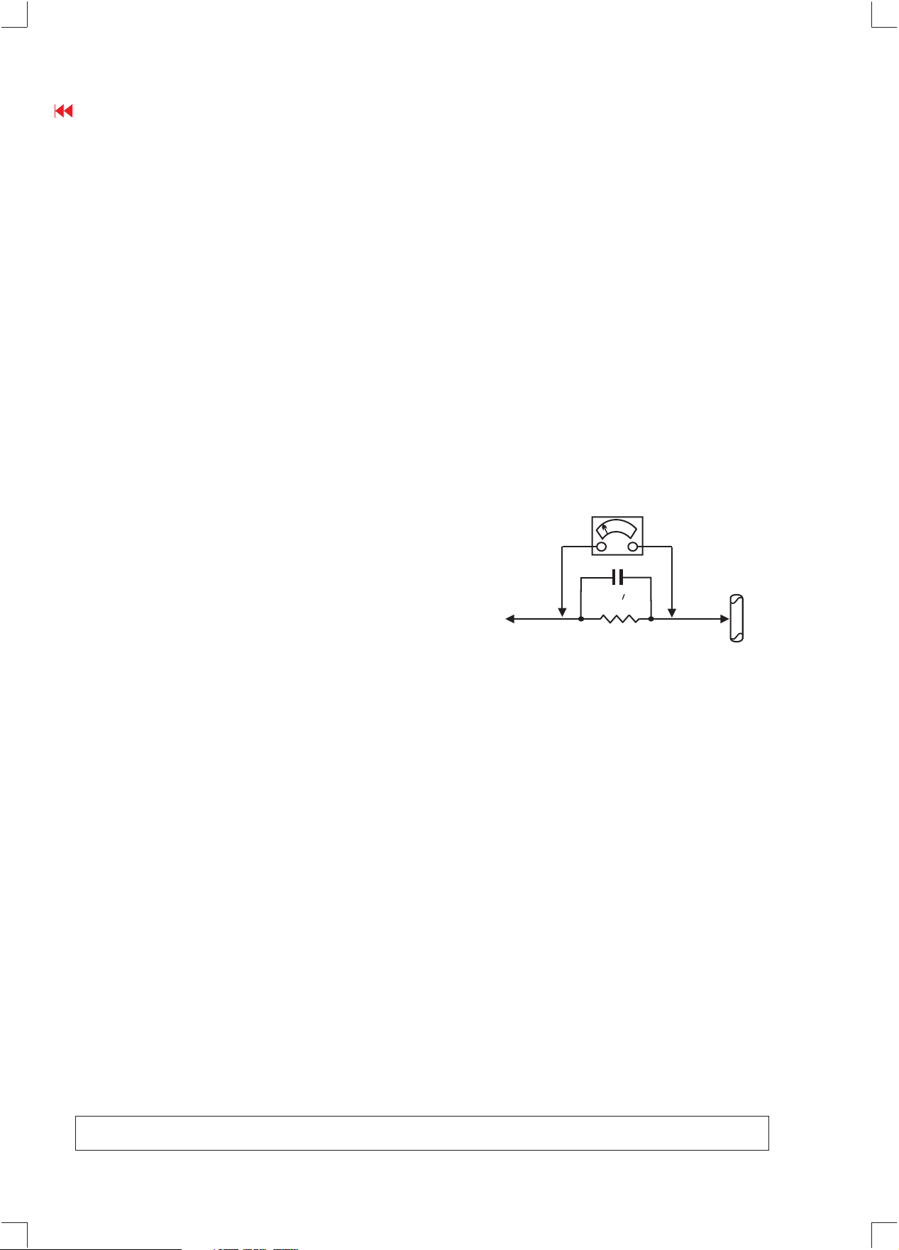
2. Connect a 1.5k, 10w resistor paralleled by a 0.15uf. capacitor between
each exposed metallic cabinet part and a good earth ground such as a
water pipe, as shown above.
3. Use an ac voltmeter with at least 5000 ohmsy volt sensitivity to measure
the potential across the resistor.
4. The potential at any point should not exceed 0.75 volts. Aleakage current
tester may be used to make this test; leakage current must not exceed
0.5 milliamps. If a measutement is outside of the specified limits, there is
a possibility of shock hazard. The receiver should be repaired and
rechecked before retutning it to the customer.
5. Repeat the above procedure with the ac plug reversed.( Note: An ac
adapter is necessary when a polarized plug is used. Do not defeat the
polarizing feature of the plug.)
Picture Tube Replacement
The primary source of X-radiation in this television receiver is the picture
tube.The picturetube utilized in this chassis is specially constructed to limit
X-radiation emissions. For continued X-radiation protection, the replacement
tube must be the same type as the original, including suffix letter,or a Philips
approved tupe.
Parts Replacement
Many electrical and mechanical parts in Philips television sets have special
safety related charcteristics. These characteristics are often not evident from
visual inspection nor can the protection afforded by them necessarily be
obtained by using replacement components rated for higher voltage, wattage,
etc. The use of a substitute part which does not have the same safety
characteristics as the Philips recommended replacement part shown in this
service manual may create shock, fire, or other hazards
1500 ohm, 10W
WATER
PIPE
EARTH
GROUND
WSRNING OFF
SERVICE NOTE
:
Before removing the CRT anode cap, turn the unit and short the HIGH VOLTAGE to the CRT DAG ground.
:
The CRT DAG is not at chassis ground.
Page 3
2
201P GS3 CM25
IMPORTANT SAFETY NOTICE
Go to cover page
Proper service and repair is important to the safe, reliable
operation of all Philips Consumer Electronics Company**
Equipment. The service procedures recommended by
Philips and described in this service manual are effective
methods of performing service operations. Some of these
service operations require the use of tools specially designed
for the purpose. The special tools should be used when and
as recommended.
It is important to note that this manual contains various
CAUTIONS and NOTICES which should be carefully read in
order to minimize the risk of personal injury to service
personnel. The possibility exists that improper
service methods may damage the equipment. It also is
important to understand that these CAUTIONS and NOTICES
ARE NOT EXHAUSTIVE. Philips could not
possibly know, evaluate and advise the service trade of all
conceivable ways in which service might be done or of the
possible hazardous consequences of each way.
Consequently, Philips has not undertaken any such broad
evaluation. Accordingly, a servicer who uses a service
procedure or tool which is not recommended by Philips must
first satisfy himself thoroughly that neither his safety nor the
safe operation of the equipment will be jeopardized by the
service method selected.
TO ENSURE THE CONTINUED RELIABILITY OF THIS
PRODUCT, USE ONLY ORIGINAL
MANUFACTURER'S REPLACEMENT PARTS, WHICH ARE
LISTED WITH THEIR PART
NUMBERS IN THE PARTS LIST SECTION OF THIS
SERVICE MANUAL.
* * Hereafter throughout this manual, Philips Consumer
Electronics Company will be referred to as Philips.
WARNING
Critical components having special safety characteristics are
identified with a by the Ref. No. in the parts list and
enclosed within a broken line*
(where several critical components are grouped in one area)
along with the safety symbol on the schematics or
exploded views.
Use of substitute replacement parts which do not have the
same specified safety characteristics may create shock, fire,
or other hazards.
Under no circumstances should the original design be
modified or altered without written permission from Philips.
Philips assumes no liability, express or implied, arising out of
any unauthorized modification of design.
Servicer assumes all liability.
* Broken Line
Back
Forward
Page 4
Technical Data
Technical Specification*
CRT
Size and deflection : 21 inch/51cm,90 defection angle
Pitch of the : Approx. 0.24 mm
Aperture grille
O
White Color Temperature
201P GS3 CM25
Go to cover page
3
Tube type :
Aperture grille, flat, high
contrast, anti-static,
anti reflection, light
transmission 40 %
Phosphor : B22
Recommended display
area : 392 x 294 mm
Maximum display area : 406.1 x 304.6 mm
Scanning
Horizontal scanning : 30 - 121 KHz
Vertical : 50 - 160 Hz
scanning
Video
Video dot rate : 320 Mhz
Input impedance
-Video : 75 Ohm
- Sync : 2.2 kOhm
Input signal levels : 0.7Vpp
Separate sync
Sync input signal
: Composite sync
Sync polarities : Positive / negative
Chromaticity CIE coordinates:
at 9300 k x = 0.283 y = 0.297
o
o
6500 k x = 0.313 y = 0.329
o
5500 k x = 0.332 y = 0.347
Physical Specifications
Dimensions : 501(W)x501.8(H)x465.8(D)mm
weight : 26 Kg
Power supply : 90 - 264 VAC, 47~63 HZ
Operating condition
Temperature : 0 C - 35 C
OO
Relative Humidety : 10%-90%(W/O Condensation)
Storage condition
Temperature : - 40 C - 60 C
OO
Relative Humidity :5%-95%(W/O Condensation)
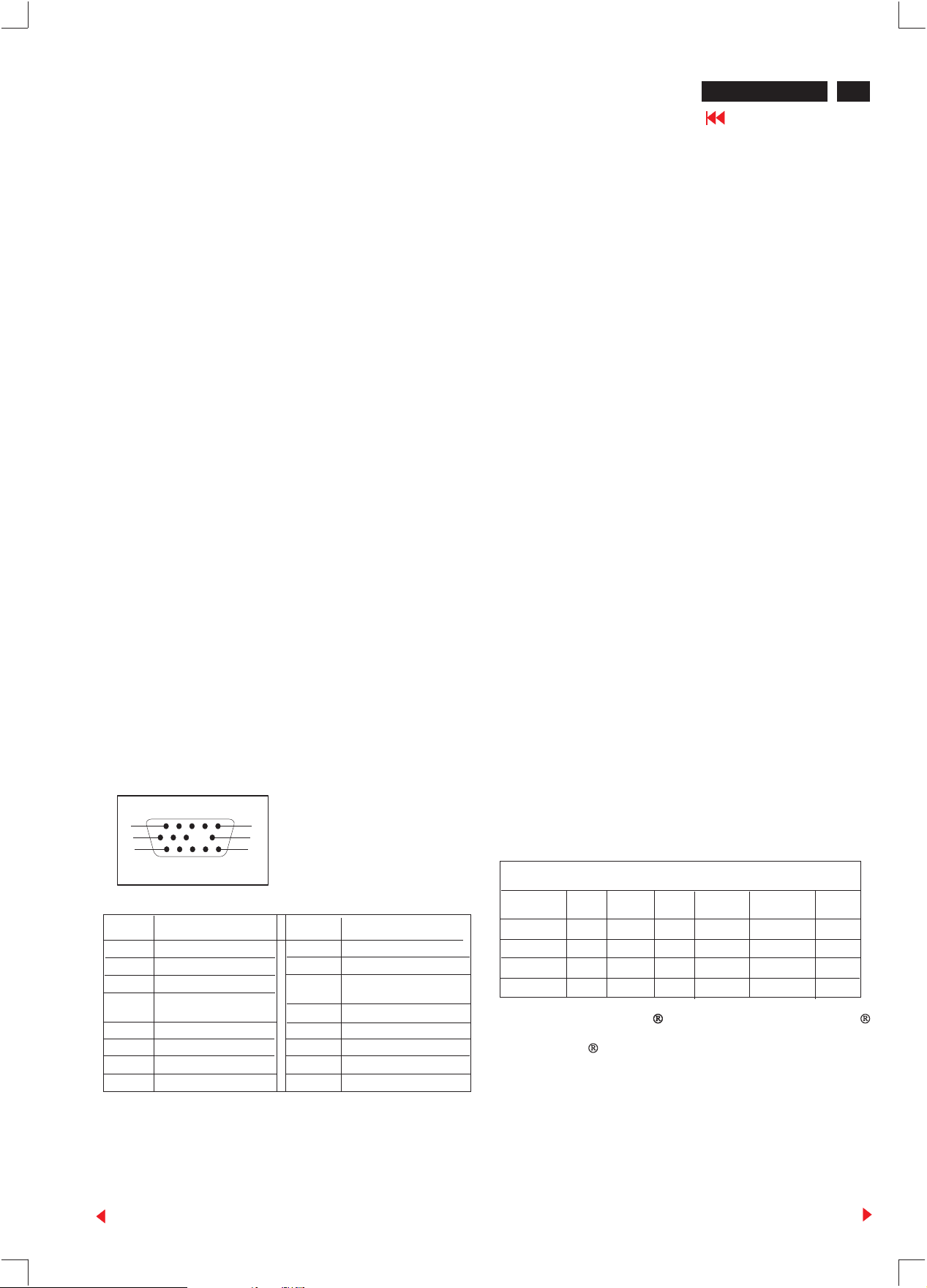
Pin assignment :
The 15-pin D-sub connector(male) of the signal cable
(IBM systems) :
1
6
11
Pin No.
1
2
3
4
5
6
7
8
Assignment
Red video input
Green video input
Blue video input
Identification output Connected to pin 10
Ground
Red video ground
Green video ground
Blue video ground
5
10
15
Pin No.
9
10
11
12
13
14
15
Assignment
No pin
Sync ground
Identification output -
Connected to pin 10
Serial data line(SDA)
H.Sync /H+V
V.Sync(VCLK for DDC)
Data clock line(SCL)
Automatic Power Saving
If you have VESA's DPMS compliance display card or
software installed in your PC,the monitor can automaticlly
reduce its power consumption when not in use. And if an
input from a keyboard, mouse or other input devices is
detected, the monitor will automatically "wake up". The
following table shows the power consumption and
signalling of this automatic power saving features :
Power Management Definition
Typical
140 W
POWER
SAVING( % )
89 %
89 %
98 %
VESA's mode
ON
Stand-by
Suspend
OFF
VIDEO
Active
Blanked
Blanked
Blanked
H-SYNC
Yes
No
Yes
No
V-SYNC
Yes
Yes
No
No
POWER
USED
<15W
<15W
<3W
This monitor is Energy Star compliant .As an ENERGY STAR
Partner, PHILIPS has determined that this product meets the
ENERGY STAR guidelines for energy efficiency.
0%
LED
COLOR
Green
Yellow
Yellow
Amber
Back
Forward
Page 5
201P GS3 CM25
4
Regulatory Information
Go to cover page
Regulatory Information
TCO'92 and TCO '99 Information
Why do we have environmentally labeled computers?
In many countries, environmental labeling has become an established
method for encouraging the adaptation of goods and services to the
environment. The main problem, as far as computers and other
electronics equipment are concerned, is that environmentally harmful
substances are used both in the products and during their manufacture.
Since it is not so far possible to satisfactorily recycle the majority of
electronics equipment, most of these potentially damaging substances
sooner or later enter nature.
There are also other characteristics of a computer, such as energy
consumption levels, that are important from the viewpoints of both the
work (internal) and natural (external) environments. Since all methods of
electricity generation have a negative effect on the environment (e.g.
acidic and climate-influencing emissions, radioactive waste), it is vital to
save energy. Electronics equipment in offices is often left running
continuously and thereby consumes a lot of energy.
What does labeling involve?
This product meets the requirements for the TCO'99 scheme which
provides for international and environmental labeling of personal
computers. The labeling scheme was developed as a joint effort by the
TCO (The Swedish Confederation of Professional Employees), Svenska
Naturskyddsforeningen (The Swedish Society for Nature Conservation)
and Statens Energimyndighet (The Swedish National Energy
Administration).
Approval requirements cover a wide range of issues: environment,
ergonomics, usability, emission of electric and magnetic fields, energy
consumption and electrical and fire safety.
The environmental demands impose restrictions on the presence and
use of heavy metals, brominated and chlorinated flame retardants,
CFCs (freons) and chlorinated solvents, among other things. The
product must be prepared for recycling and the manufacturer is obliged
to have an environmental policy which must be adhered to in each
country where the company implements its operational policy.
The energy requirements include a demand that the computer and/or
display, after a certain period of inactivity, shall reduce its power
consumption to a lower level in one or more stages. The length of time
to reactivate the computer shall be reasonable for the user.
Labeled products must meet strict environmental demands, for example,
in respect of the reduction of electric and magnetic fields, physical and
visual ergonomics and good usability.
Below you will find a brief summary of the environmental requirements
met by this product. The complete environmental criteria document may
be ordered from:
Environmental Requirements
Flame retardants
Flame retardants are present in printed circuit boards, cables, wires,
casings and housings. Their purpose is to prevent, or at least to delay
the spread of fire. Up to 30% of the plastic in a computer casing can
consist of flame retardant substances. Most flame retardants contain
bromine or chloride, and those flame retardants are chemically related
to another group of environmental toxins, PCBs. Both the flame
retardants containing bromine or chloride and the PCBs are suspected
of giving rise to severe health effects, including reproductive damage in
fish-eating birds and mammals, due to the bio-accumulative* processes.
Flame retardants have been found in human blood and researchers fear
that disturbances in fetus development may occur.
The relevant TCO'99 demand requires that plastic components
weighing more than 25 grams must not contain flame retardants with
organically bound bromine or chlorine. Flame retardants are allowed in
the printed circuit boards since no substitutes are available.
Cadmium**
Cadmium is present in rechargeable batteries and in the colorgenerating layers of certain computer displays. Cadmium damages the
nervous system and is toxic in high doses. The relevant TCO'99
requirement states that batteries, the color-generating layers of display
screens and the electrical or electronics components must not contain
any cadmium.
Mercury**
Mercury is sometimes found in batteries, relays and switches. It
damages the nervous system and is toxic in high doses. The relevant
TCO'99 requirement states that batteries may not contain any mercury.
It also demands that mercury is not present in any of the electrical or
electronics components associated with the labeled unit.
CFCs (freons)
The relevant TCO'99 requirement states that neither CFCs nor HCFCs
may be used during the manufacture and assembly of the product.
CFCs (freons) are sometimes used for washing printed circuit boards.
CFCs break down ozone and thereby damage the ozone layer in the
stratosphere, causing increased reception on earth of ultraviolet light
with increased risks e.g. skin cancer (malignant melanoma) as a
consequence.
Lead**
Lead can be found in picture tubes, display screens, solders and
capacitors. Lead damages the nervous system and in higher doses,
causes lead poisoning. The relevant TCO'99 requirement permits the
inclusion of lead since no replacement has yet been developed.
* Bio-accumulative is defined as substances which accumulate within
living organisms.
** Lead, Cadmium and Mercury are heavy metals which are bioaccumulative.
Energy Star Declaration
This monitor is equipped with a function for saving energy which
supports the VESA Display Power Management Signaling (DPMS)
standard. This means that the monitor must be connected to a
computer which supports VESA DPMS to fulfill the requirements in the
NUTEK specification 803299/94. Time settings are adjusted from the
system unit by software. From indicated inactivity to Power Saving
Position A2, the total time must not be set to more than 70 minutes.
NUTEK
Federal Communications Commission (FCC) Notice (U.S. Only)
This equipment has been tested and found to comply with the limits for a Class B digital device,
pursuant to Part 15 of the FCC Rules. These limits are designed to provide reasonable
protection against harmful interference in a residential installation. This equipment generates,
uses and can radiate radio frequency energy and, if not installed and used in accordance with
the instructions, may cause harmful interference to radio communications. However, there is no
guarantee that interference will not occur in a particular installation. If this equipment does cause
harmful interference to radio or television reception, which can be determined by turning the
equipment off and on, the user is encouraged to try to correct the interference by one or more of
the following measures:
Reorient or relocate the receiving antenna.
Increase the separation between the equipment and receiver.
!
Connect the equipment into an outlet on a circuit different from that to which the receiver
!
!
for compliance could void the user's authority to operate the equipment.
Use only RF shielded cable that was supplied with the monitor when connecting this monitor to a
computer device.
To prevent damage which may result in fire or shock hazard, do not expose this appliance to rain
or excessive moisture.
THIS CLASS B DIGITALAPPARATUS MEETS ALL REQUIREMENTS OF THE CANADIAN
INTERFERENCE-CAUSING EQUIPMENT REGULATIONS.
is connected.
Consult the dealer or an experienced radio/TV technician for help.
Changes or modifications not expressly approved by the party responsible
Back
Forward
Page 6
Front View
Installation
Rear View
201P GS3 CM25
Go to cover page
5
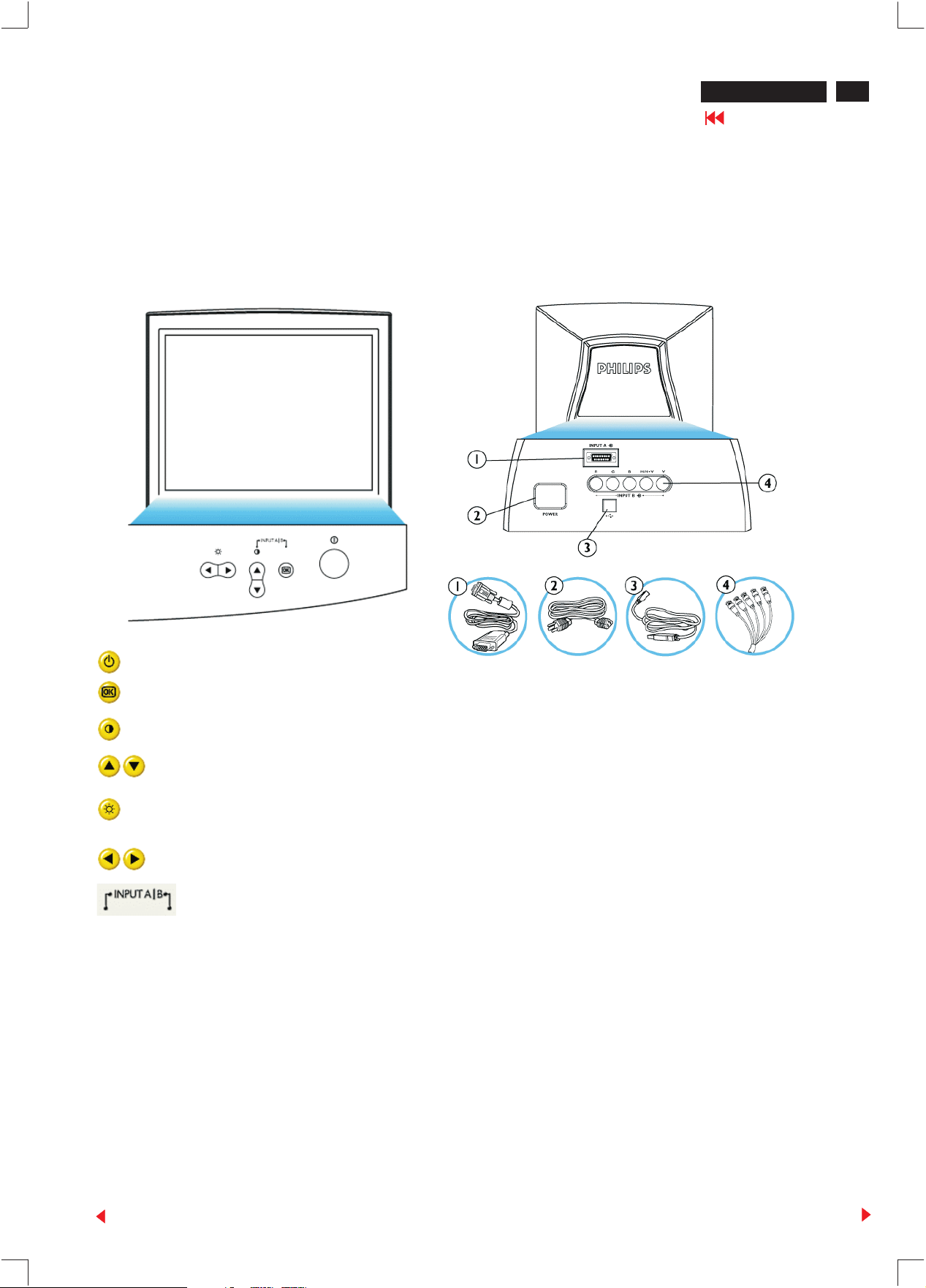
Power button switches your monitor on.
OK button which when pressed will take you to
the OSD controls
Contrast hotkey. When the UP arrow is pressed,
the adjustment controls for the CONTRAST will
show up.
UP and DOWN buttons are used when adjusting
the OSD of your monitor
Brightness hotkey. When both the LEFT and
RIGHT arrows are pressed at the same time,
then the adjustment controls for BRIGHTNESS
will show up.
LEFT and RIGHT buttons, like the UP and
DOWN buttons, are also used in adjusting the
OSD of your monitor.
By pressing both the UP and OK buttons, you
can easily access the Input Signals A and/or B.
1. D-Sub Port - Attach the D-Sub connector that comes with your
monitor here. Other end connects to your PC.
2. Power in - Attach power cable here.
3. USB Port - Attach your USB Upstream cable here. Connect the
other end to your USB hub or your PC's USB connector.
4. BNC Connectors - Attach the connectors here to get the best video
performance from your monitor
Back
Forward
Page 7
6
201P GS3 CM25
Go to cover page
OSD Adjustment
Data Storage(Resolution Modes)
Factory preset modes:
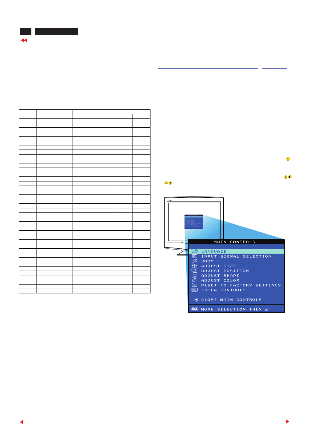
This monitor has 39 factory-preset modes
On-Screen Display
Description of the On-Screen Display The OSD
Tree The OSD Controls
as indicated in the following table:
Description of the On Screen Display
What is the On-Screen Display?
Mode H(KHz) / V(Hz) H V
1+2-3-+
4-5-6+7++
8-+
9-10 + +
11 + +
12 - 13 + +
14 - 15 + +
16 - 17 + +
18 + +
19 + +
20 + +
21 + +
22 + +
23 - 24 + +
25 + +
26 + +
27 + +
28 + +
29 + +
30 + +
31 + +
32 + +
33 + +
34 + +
35 + +
36 + +
37 + +
38 +
39 + +
Resolution
640 X 350
640 X 480
720 X 400 31.468KHz/70.084 Hz
640 X 480
640 X 480
640 X 350
800 X 600
720 X 400
640 X 480
800 X 600
800 X 600
1024 X 768
832 X 624
640 X 480
800 X 600
1024 X 768
1280 X 960
1024 X 768
800 X 600
1280 X 1024
1152 X 864
1024 X 768
1152 X 870
1152 X 900
1600 X 1200
1280 X 1024
1600 X 1200
1792X 1344 83.640 KHz/59.999 Hz
1280 X 960
1856X 1392 86.333 KHz/59.995 Hz
1600 X 1200 87.500 KHz/70.000 Hz
1920X 1440 90.000 KHz/60.000 Hz
1280 X 1024 91.146KHz/85.024Hz
1600 X 1200 93.750KHz/75.000Hz
1600 X 1200 106.250KHz/85.000Hz
1792 X 1344
2048 X 1536 95.820 KHz/60.000 Hz
1920 X 1440 112.50 KHz/75.000 Hz
2048 X 1536 120.45 KHz/75.000 Hz
Frequency Sync. polarity
31.469 KHz/70.087Hz
31.469KHz/59.941 Hz
37.5 KHz/75Hz
37.861 KHz/72.810 Hz
37.861 KHz/85.081 Hz
37.879 KHz/60.317 Hz
37.927 KHz/85.039 Hz
43.269 KHz/85.008 Hz
46.875 KHz/75.000 Hz
48.077 KHz/72.188 Hz
48.363KHz/60.004Hz
49.722 KHz/74.546Hz
50.628 KHz/100.10 Hz
53.674 KHz/85.061 Hz
56.476 KHz/70.069 Hz
60.000 KHz/60.000 Hz
60.023KHz/75.029Hz
63.923 KHz/100.00 Hz
63.981KHz/60.020Hz
67.500 KHz/75.000 Hz
68.677KHz/84.997Hz
68.681KHz/74.979Hz
71.809KHz/76.15Hz
75.000 KHz/60.000 Hz
79.976KHz/75.024Hz
81.250 KHz/65.000 Hz
85.938 KHz/85.002 Hz
106.270 KHz/74.997 Hz
+
This is a feature in all Philips monitors which allows an
end-user to adjust screen performance of monitors
directly though an on-screen instruction window. The user
interface provides user-friendliness and ease-of-use
when operating the monitor.
Basic and simple instruction on the control keys.
On the front controls of your monitor, once you press the
button, the On Screen Display (OSD) Main Controls
window will pop up and you can now start making
adjustments to your monitor's various features. Use the
or the keys to make your adjustments within.
Back
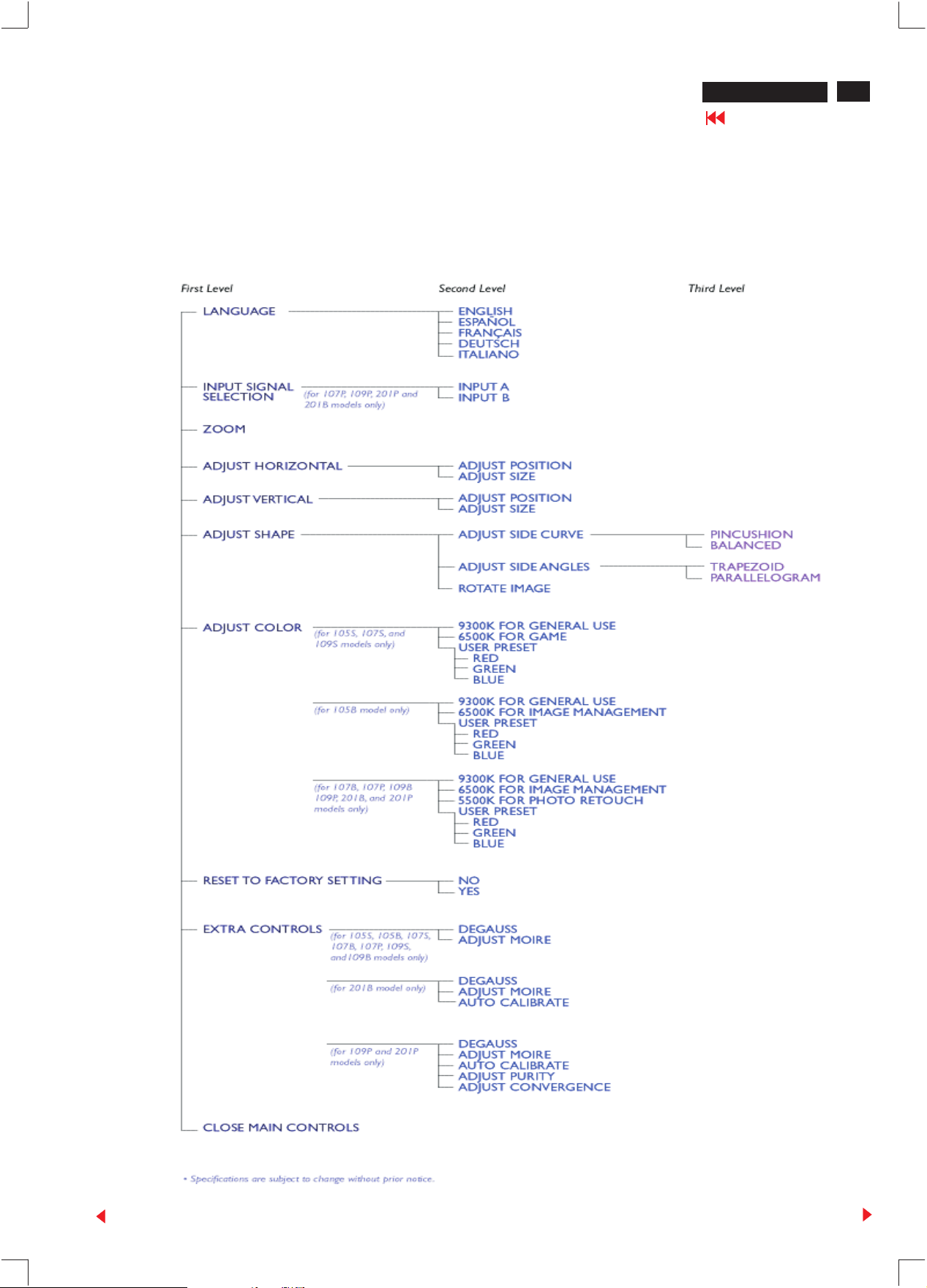
The OSD Tree
Below is an overall view of the structure of the On-Screen
Display. You can use this as reference when you want to
later on work your way around the different adjustments.
Forward
Page 8
OSD menu tree structure
The OSD Tree
Below is an overall view of the structure of the OnScreen Display. You can use this as reference when you
want to later on work your way around the different
adjustments.
201P GS3 CM25
Go to cover page
7
Back
Forward
Page 9
8
201P GS3 CM25
Go to cover page
OSD Adjustments
The OSD Controls
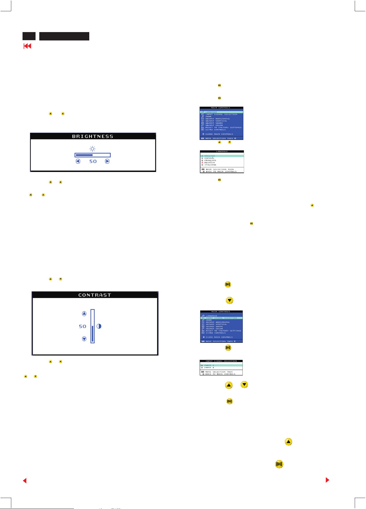
BRIGHTNESS
To adjust your screen's brightness, follow the steps below. Brightness is
the overall intensity of the light coming from the screen. A 50%
brightness is recommended.
1) Press the or button on the monitor. The BRIGHTNESS window
appears.
2) Press the or button to adjust the brightness.
3) When the brightness is adjusted to the level desired, stop pressing
the or button and after three seconds the BRIGHTNESS window
will disappear with the new adjustment saved.
Smart Help
continue to the CONTRAST window, follow the steps under
CONTRAST.
CONTRAST
To adjust your screen's contrast, follow the steps bellow. Contrast is the
difference between the light and dark areas on the screen. A 100%
contrast is recommended.
1) Press the or button on the monitor. The CONTRAST window
appears.
After the BRIGHTNESS window has disappeared, to
LANGUAGE
The ON SCREEN DISPLAY shows its settings in one of five
languages. The default is English, but you can select French,
Spanish, German, or Italian.
1) Press the button on the monitor. The MAIN CONTROLS
window appears. LANGUAGE should be highlighted.
2) Press the button again. The LANGUAGE window
appears.
3) Press the or button until the desired language is
highlighted.
4) Press the button to confirm your selection and return to
MAIN CONTROLS window. CLOSE MAIN CONTROLS will be
highlighted...
Smart Help
...tocontinue to INPUT SIGNAL SELECTION, press the
button until INPUT SIGNAL SELECTION is highlighted. Next,
follow steps3-5under INPUT SIGNAL SELECTION.
...toexit completely, press the button
After returning to MAIN CONTROLS...
INPUT SIGNAL SELECTION (Not available in
all models)
INPUT SIGNAL SELECTION determines what
you see on the screen. The default setting is
INPUT A, but if the video input signal is different
that the output signal, you may want to change it
to INPUT B.?
1) Press the button on the monitor. The MAIN
CONTROLS window appears.
2) Press the button until INPUT SIGNAL
SELECTION is highlighted.
2) Press the or button to adjust the contrast.
3) When the contrast is adjusted to the level desired, stop pressing the
or button and after three seconds the CONTRAST window will
disappear with the new adjustment saved.
Smart Help
continue to the MAIN CONTROLS, follow the steps under LANGUAGE
After the CONTRAST window has disappeared, to
Back
3) Press the button. The INPUT SIGNAL
SELECTION window appears.
4) Press the or button to highlight INPUT
B or INPUT A.
5) Press the button to confirm your selection
and return to the MAIN CONTROLS window.
CLOSE MAIN CONTROLS will be highlighted.
Smart Help
After returning to MAIN
CONTROLS...
...tocontinue to ZOOM, press the button
until ZOOM is highlighted. Next, follow steps 3 5 under ZOOM.
...toexit completely, press the button
Forward
Page 10
OSD Adjustments
201P GS3 CM25
Go to cover page
9
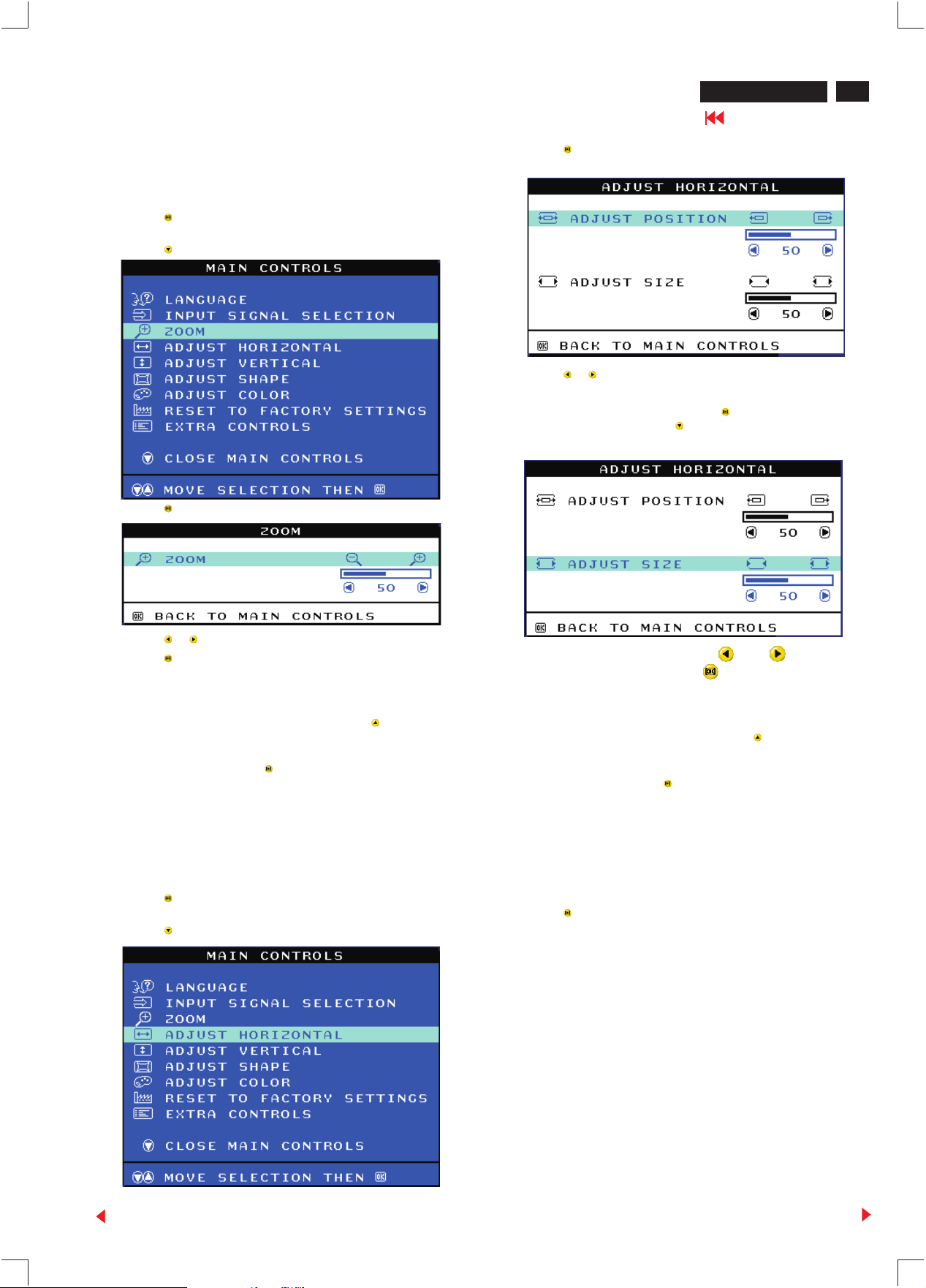
ZOOM
ZOOM increases or decreases the size of the images on your screen.
To adjust the ZOOM follow the steps below.
1) Press the button on the monitor. The MAIN CONTROLS window
appears.
2) Press the button until ZOOM is highlighted.
3) Press the button. The ZOOM window appears.
3) Press the button. The ADJUST HORIZONTAL window appears.
ADJUST POSITION should be highlighted.
4) Press the or button to move the image to the left or right.
5) When the position is adjusted, press the button to return to MAIN
CONTROLS window, or press the to highlight ADJUST SIZE.
4) Press the or button to adjust ZOOM.
5) Press the button to confirm your selection and return to the MAIN
CONTROLS window. CLOSE MAIN CONTROLS will be highlighted.
Smart Help
...tocontinue to ADJUST HORIZONTAL, press the button until
ADJUST HORIZONTAL is highlighted. Next, follow steps3-7under
ADJUST HORIZONTAL.
...toexit completely, press the button
ADJUST HORIZONTAL
ADJUST POSITION under ADJUST HORIZONTAL shifts the image on
your screen either to the left or right. Use this feature if your image
does not appear centered. ADJUST SIZE under ADJUST
HORIZONTAL expands or controls the image on your screen, pushing it
out toward the left and right sides or pulling it in toward the center.
1) Press the button on the monitor. The MAIN CONTROLS window
appears.
2) Press the button until ADJUST HORIZONTAL is highlighted.
After returning to MAIN CONTROLS...
6) To adjust the horizontal size, press th or button.
7) When the size is adjusted, press the button to return to MAIN
CONTROLS window. CLOSE MAIN CONTROLS will be highlighted.
Smart Help
...tocontinue to ADJUST VERTICAL, press the button until ADJUST
VERTICAL is highlighted. Next, start with step 3 under ADJUST
VERTICAL and follow the directions.
...toexit completely, press the button
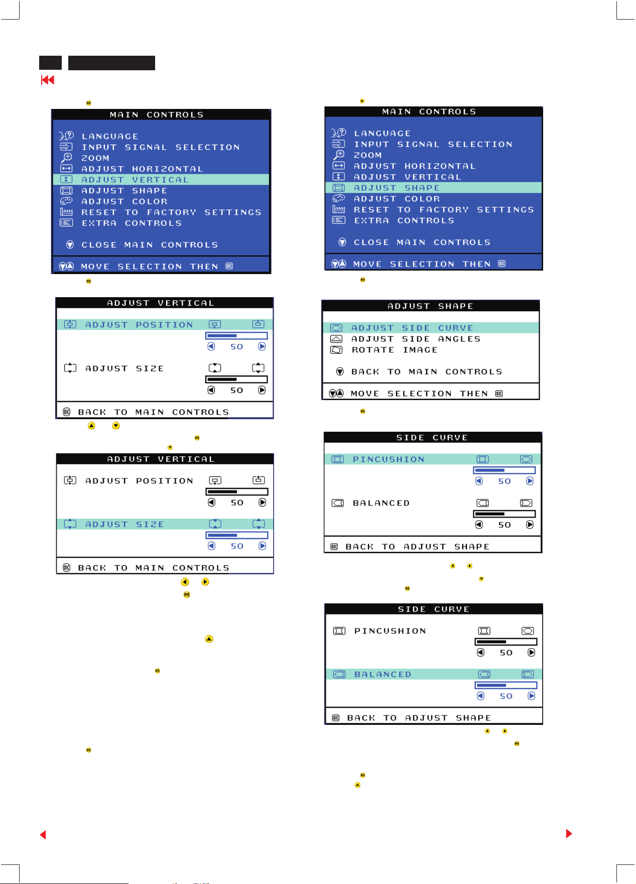
ADJUST VERTICAL
ADJUST POSITION under ADJUST VERTICAL shifts the image on
your screen either up or down. Use this feature if your image does not
appear centered. ADJUST SIZE under ADJUST VERTICAL expands or
controls the image on your screen, pushing it out toward the top or
bottom or pulling it in toward the center.
1) Press the button on the monitor. The MAIN CONTROLS window
appears.
After returning to MAIN CONTROLS...
Back
Forward
Page 11
10
201P GS3 CM25
Go to cover page
OSD Adjustments
2) Press the button until ADJUST VERTICAL is highlighted.
3) Press the button. The ADJUST VERTICAL window appears.
ADJUST POSITION should be highlighted.
2) Press the button until ADJUST SHAPE is highlighted.
3) Press the button. The ADJUST SHAPE window appears. ADJUST
SIDE CURVE should be highlighted.
4) Press the or button to move the image up or down.
5) When the position is adjusted, press the button to return to MAIN
CONTROLS window, or press the to highlight ADJUST SIZE.
6) To adjust the vertical size, press the or button.
7) When the size is adjusted, press the button to return to MAIN
CONTROLS window. CLOSE MAIN CONTROLS will be highlighted.
Smart Help
...tocontinue to ADJUST SHAPE, press the button until ADJUST
SHAPE is highlighted. Next, start with step 3 under ADJUST SHAPE
and follow the directions.
...toexit completely, press the button
ADJUST SHAPE
ADJUST SIDE CURVE
ADJUST SIDE CURVE under ADJUST SHAPE allows you to adjust two
of the five preset options. These two options are PINCUSHION and
BALANCED pincushion. Note: use these features only when the picture
is not square.
1) Press the button on the monitor. The MAIN CONTROLS window
appears.
After returning to MAIN CONTROLS...
4) Press the button. The SIDE CURVE window appears.
PINCUSHION should be highlighted.
5) To adjust the pincushion, press the or button.
6) When the pincushion is adjusted, press the button to highlight
BALANCED or press the button to return to the ADJUST SHAPE
window.
7) To adjust the balanced pincushion, press the or button.
8) When the balanced pincushion is adjusted, press the button to
return to the ADJUST SHAPE window. BACK TO MAIN WINDOWS will
be highlighted.
9) Press the button to return to the MAIN CONTROLS window, or
press the button until ADJUST SIDE ANGLES is highlighted.
Back
Forward
Page 12
OSD Adjustments
201P GS3 CM25
Go to cover page
11
Smart Help After returning to MAIN CONTROLS...
...to continue to ADJUST SIDE ANGLES, start with step 5 under
ADJUST SIDE ANGLES and follow the directions.
...to exit completely, press the button twice.
...to adjust only the BALANCED pincushion, follow steps1-4above,
then press the button, and follow steps7-9.
...to adjust only the PARALLELOGRAM, follow steps1-4above, then
press the button, and follow steps 7 -9
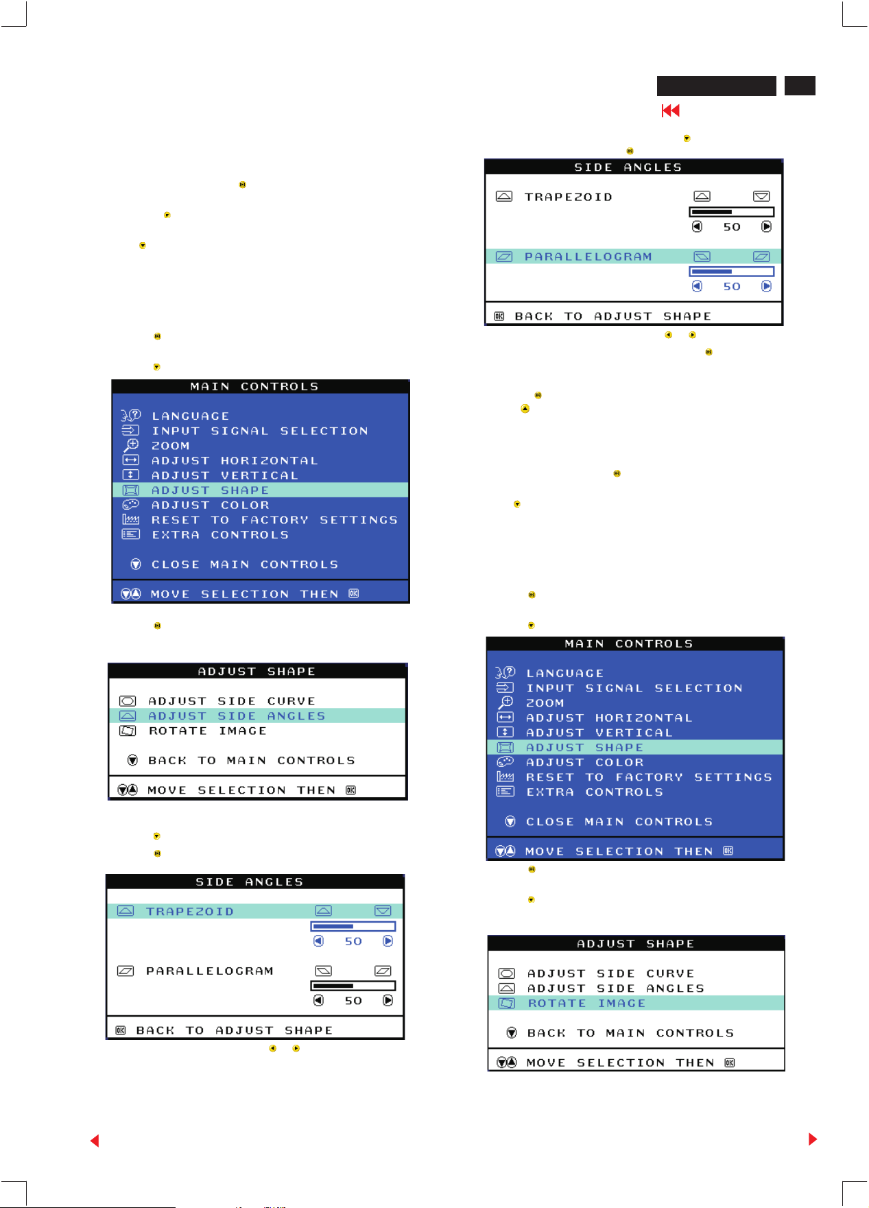
ADJUST SIDE ANGLES
ADJUST SIDE ANGLES under ADJUST SHAPE allows you to adjust
two of the five preset options. These two options are TRAPEZOID and
PARALLELOGRAM. Note: use these features only when the picture is
not square.
1) Press the button on the monitor. The MAIN CONTROLS window
appears.
2) Press the button until ADJUST SHAPE is highlighted.
3) Press the button. The ADJUST SHAPE window appears. ADJUST
SIDE CURVE should be highlighted.
7) When the trapezoid is adjusted, press the button to highlight
PARALLELOGRAM or press the button to return to the ADJUST
8) To adjust the parallelogram, press the or button.
9) When the parallelogram is adjusted, press the button to return to
the ADJUST SHAPE window. BACK TO MAIN WINDOWS will be
highlighted.
10) Press the button to return to the MAIN CONTROLS window, or
press the button until ROTATE IMAGE is highlighted.
Smart Help
...to continue to ROTATE IMAGE, start with step 5 under ROTATE
IMAGE and follow the directions.
...to exit completely, press the button twice.
...to adjust only the PARALLELOGRAM, follow steps1-4above, then
press the button, and follow steps 7 -9
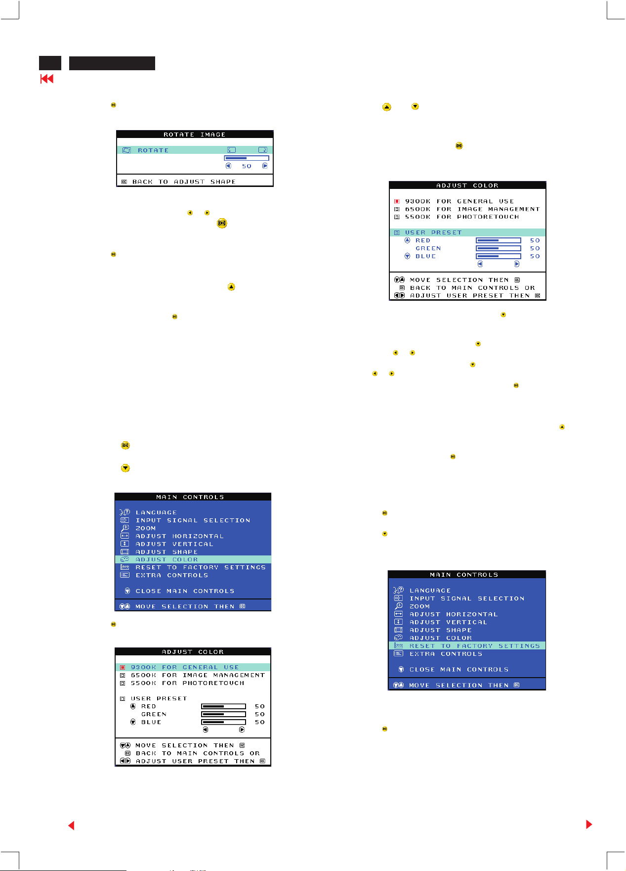
ROTATE IMAGE
ROTATE IMAGE under ADJUST SHAPE allows you to adjust one of
the five preset options. These two options are PINCUSHION and
BALANCED pincushion. Note: use this feature only when the picture is
not square.
1) Press the button on the monitor. The MAIN CONTROLS window
appears.
2) Press the button until ADJUST SHAPE is highlighted.
After returning to MAIN CONTROLS...
4) Press the button to highlight ADJUST SIDE ANGLES.
5) Press the button. The SIDE ANGLES window appears.
TRAPEZOID should be highlighted.
6) To adjust the trapezoid, press the or button.
SHAPE window.
Back
3) Press the button. The ADJUST SHAPE window appears. ADJUST
SIDE CURVE should be highlighted.
4) Press the arrow until ROTATE IMAGE is highlighted.
Forward
Page 13
12
201P GS3 CM25
Go to cover page
OSD Adjustments (Continued)
5) Press the button. The ROTATE IMAGE window appears. ROTATE
should be highlighted.
6) To adjust the rotation, press the or button.
7) When the rotation is adjusted, press the button to return to the
ADJUST SHAPE window. BACK TO MAIN CONTROLS should be
highlighted.
8) Press the button to return to MAIN CONTROLS.
Smart Help
...tocontinue to ADJUST COLOR, press the button until ADJUST
COLOR is highlighted. Next, start with step 3 under ADJUST COLOR
and follow the directions.
...to exit completely, press the button twice.
After returning to MAIN CONTROLS...
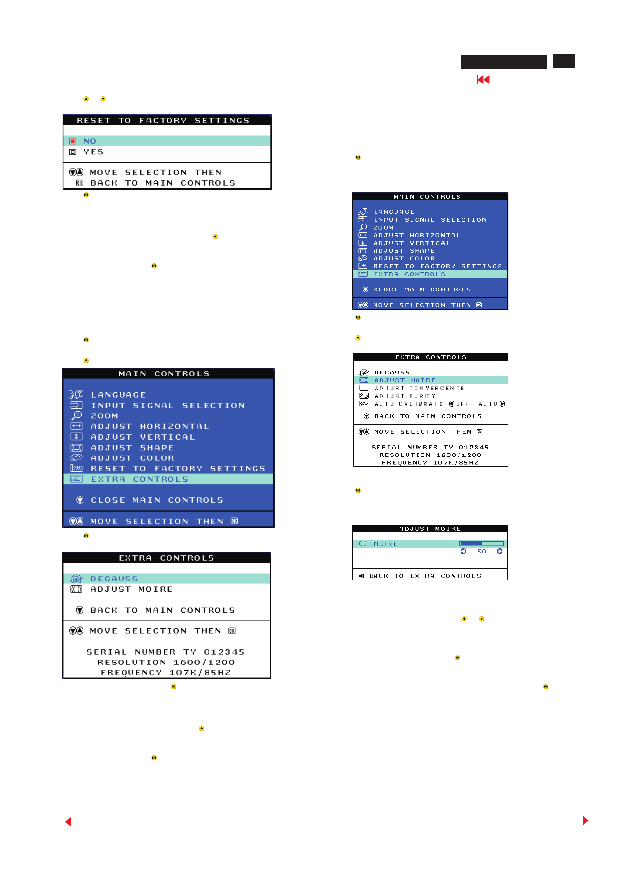
ADJUST COLOR
Your monitor has three preset options you can choose from. The first
option is for GENERAL USE, which is fine for most applications. The
second option is for IMAGE MANAGEMENT, which includes projects
such as desktop publishing, viewing a DVD from your DVD player or
pictures on the World Wide Web, and playing video games. The third
option is for PHOTO RETOUCH, which is for working with pictures you
have imported into your computer and want to alter. When you select
one of these options, the monitor automatically adjusts itself to that
option. There is also a fourth option, USER PRESET, which allows you
to adjust the colors on your screen to a setting you desire.
1) Press the button on the monitor. The MAIN
CONTROLS window appears.
2) Press the button until ADJUST COLOR is highlighted
4) Press the or button to highlight 9300K for GENERAL USE,
6500K for IMAGE MANAGEMENT, 5500K for PHOTO RETOUCH, or
USER PRESET.
5) Once you have highlighted GENERAL USE, IMAGE MANAGEMENT,
or PHOTO RETOUCH, press the button to confirm you selection and
return to the MAIN CONTROLS window. CLOSE MAIN CONTROLS will
be highlighted.
6a) If USER PRESET is highlighted, press the button to highlight
RED. Next, press the LEFT CURSOR or RIGHT CURSOR button to
adjust the color red.
6b) When finished with RED, press the button to highlight GREEN.
Next, press the or button to adjust the color green.
6c) When finished GREEN, press the button to highlight BLUE. Next,
press the or button to adjust the color blue.
6d) When all adjustments are complete, press the button to confirm
your adjustments and return to the MAIN CONTROLS window. CLOSE
MAIN CONTROLS will be highlighted.
Smart Help
...tocontinue to RESET TO FACTORY SETTINGS, press the button
until RESET TO FACTORY SETTINGS is highlighted. Next, start with
step 3 under RESET TO FACTORY SETTINGS.
...toexit completely, press the button.
RESET TO FACTORY SETTINGS
RESET TO FACTORY SETTINGS returns everything in all the windows
to factory presets.
1) Press the button on the monitor. The MAIN CONTROLS window
appears.
2) Press the button until RESET TO FACTORY SETTINGS is
highlighted.
After returning to MAIN CONTROLS. . .
3) Press the button. The ADJUST COLOR window appears.
Back
3) Press the button. The RESET TO FACTORY SETTINGS window
appears.
Forward
Page 14
OSD Adjustments (Continued)
201P GS3 CM25
Go to cover page
13
4) Press the or button to select YES or NO. NO is the default. YES
returns all settings to their original factory adjustments.
5) Press the button to confirm your selection and return to the MAIN
CONTROLS window. CLOSE MAIN CONTROLS will be highlighted.
Smart Help
...tocontinue to EXTRA CONTROLS, press the button until EXTRA
CONTROLS is highlighted. Next, start with step 3 under EXTRA
CONTROLS.
...toexit completely, press the button.
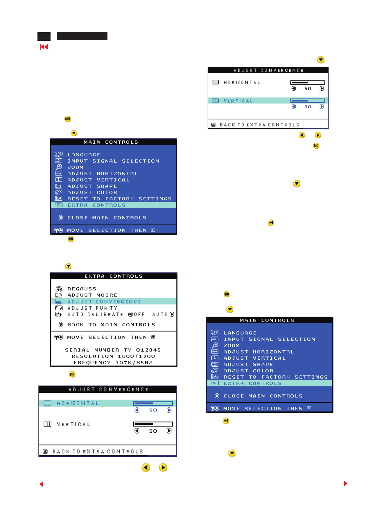
EXTRA CONTROLS
DEGAUSS
EXTRA CONTROLS is a set of three features, including DEGAUSS.
Degaussing removes electromagnetic build up that may distort the color
on your screen.
1) Press the button on the monitor. The MAIN CONTROLS window
appears.
2) Press the button until EXTRA CONTROLS is highlighted.
After returning to MAIN CONTROLS...
ADJUST MOIRE
EXTRA CONTROLS is a set of three features, including ADJUST
MOIRE. Moire is a fringe pattern arising from the interference between
two superimposed line patterns. To adjust your moire, follow the steps
below. Note: Use only if necessary. By activating ADJUST MOIRE,
sharpness can be affected.
1) Press the button on the monitor. The MAIN CONTROLS window
appears.
2) Press the DOWN CURSOR button until EXTRA CONTROLS is
highlighted.
3) Press the button. The EXTRA CONTROLS window appears.
DEGAUSS will be highlighted.
4) Press the button until ADJUST MOIRE is highlighted.
3) Press the button. The EXTRA CONTROLS window appears.
DEGAUSS will be highlighted.
4) To degauss your screen, press the button. Your screen will be
degaussed, then the MAIN CONTROLS window will reappear. CLOSE
MAIN CONTROLS will be highlighted.
Smart Help
...tocontinue to ADJUST MOIRE, press the button until EXTRA
CONTROLS is highlighted. Next, start with step 3 under EXTRA
CONTROLS, ADJUST MOIRE.
...toexit completely, press the button.
After returning to MAIN CONTROLS...
5) Press the button. The ADJUST MOIRE window appears.
HORIZONTAL will be highlighted.
6) To adjust the horizontal moire, press the or button.
7) When the moire is adjusted, press the button to return to the
EXTRA CONTROLS window. BACK TO MAIN CONTROLS will be
highlighted.
After returning to MAIN CONTROLS to exit completely, press the
button.
Back
Forward
Page 15
14
201P GS3 CM25
6
Go to cover page
OSD Adjustments (Continued)
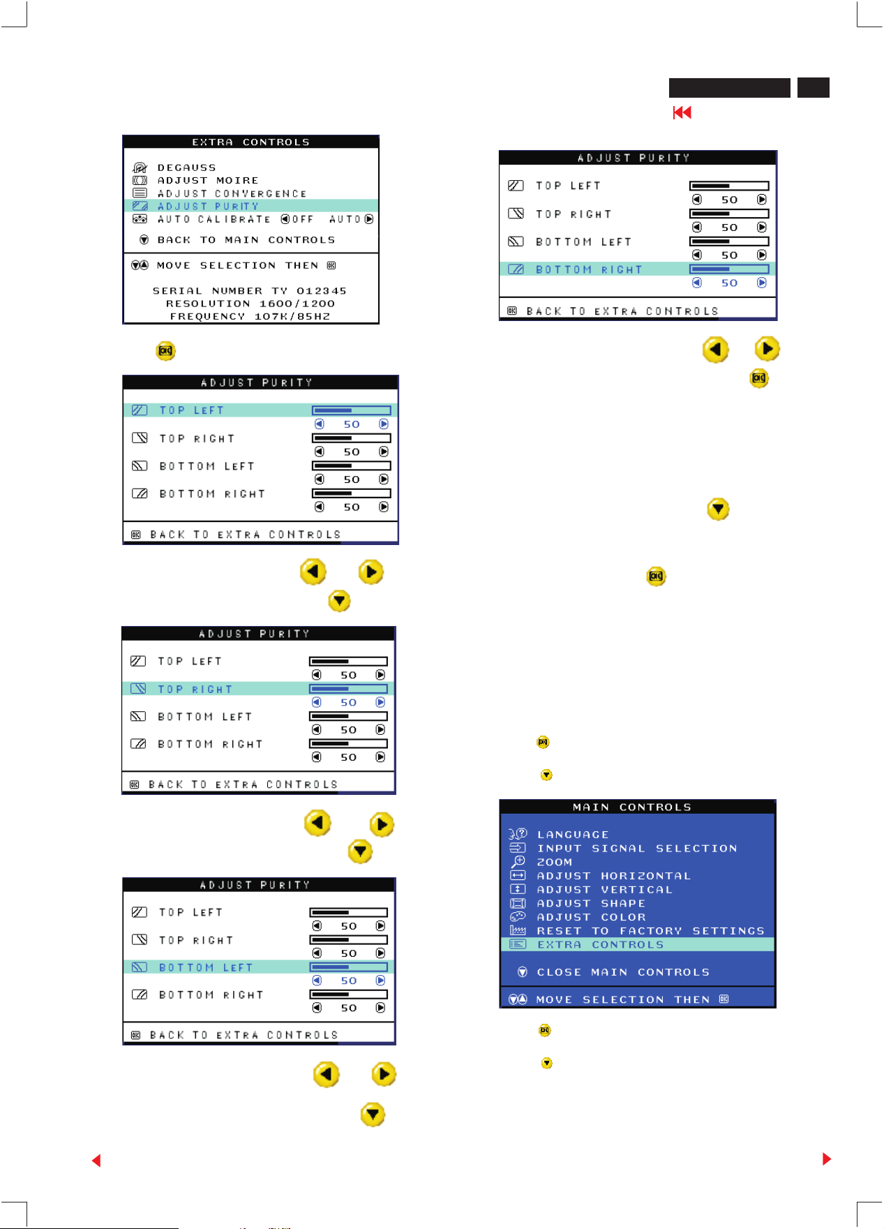
ADJUST CONVERGENCE
EXTRA CONTROLS is a set of features, including ADJUST
CONVERGENCE. Convergence is a process by which a color is
created by blending other colors. For example, white is created by
blending red, blue, and green. If these colors do not completely blend
together (converge) then you may see unwanted red, green, or blue
lines or dots. To adjust the convergence, follow the steps below. Note:
Use only if necessary. Remember: you must degauss the monitor
BEFORE adjusting the convergence.
1) Press the button on the monitor. The MAIN CONTROLS window
appears.
2) Press the button until EXTRA CONTROLS is highlighted.
7) When the horizontal convergence is adjusted, press the button to
highlight VERTICAL CONVERGENCE.
8) To adjust the vertical convergence, press the or button.
9) When the vertical convergence is adjusted, press the button to
return to the EXTRA CONTROLS window. BACK TO MAIN
CONTROLS is highlighted.
Smart Help
After returning to EXTRA CONTROLS...
...tocontinue to ADJUST PURITY, press the button until ADJUST
PURITY is highlighted. Next, start with step 4 under EXTRA
CONTROLS - ADJUST PURITY.
Note: If you have not degaussed the monitor, please follow the steps
under the Extra Controls - Degauss section of this manual before
adjusting the purity.
...toexit completely, press the button twice.
3) Press the button. The EXTRA CONTROLS window appears.
DEGAUSS is highlighted. Note: If you have not degaussed the monitor,
please follow the steps under the Extra Controls - Degauss section of
this manual before adjusting the convergence.
4) Press the button until ADJUST CONVERGENCE is highlighted.
5) Press the button. The ADJUST CONVERGENCE window
appears. ADJUST HORIZONTAL is highlighted.
ADJUST PURITY
EXTRA CONTROLS is a set of features, including ADJUST PURITY.
Purity is a process by which colors appear clear and untainted,
especially in the four corners of the monitor. Purity can be affected by
such things as the presence of a magnetic source near the monitor or
even by the ambient room temperature. For example, you might see the
color red in a corner of the monitor screen where you should see only a
pure white. To adjust the purity, follow the steps below. Note: Use only if
necessary. Remember: you must degauss the monitor BEFORE
adjusting the purity.
1) Press the button on the monitor. The MAIN CONTROLS window
appears.
2) Press the button until EXTRA CONTROLS is highlighted.
6) To adjust the horizontal convergence, press the or button.
Back
3) Press the button. The EXTRA CONTROLS window appears.
DEGAUSS is highlighted. Note: If you have not degaussed the monitor,
please follow the steps under the Extra Controls - Degauss section of
this manual before adjusting the purity.
4) Press the button until ADJUST PURITY is highlighted.
Forward
Page 16
OSD Adjustments (Continued)
201P GS3 CM25
Go to cover page
15
5) Press the . The ADJUST PURITY window appears. TOP LEFT is
highlighted.
6) To adjust the top left purity, press the or button.
7) When the top left purity is adjusted, press the button to highlight
TOP RIGHT.
12) To adjust the bottom right purity, press the or button.
13) When the bottom right purity is adjusted, press the button
to return to the EXTRA CONTROLS window. BACK TO MAIN
CONTROLS is highlighted.
Smart Help
After returning to EXTRA CONTROLS...
...tocontinue to ADJUST PURITY, press the button until AUTO
CALIBRATE is highlighted. Next, start with step 4 under EXTRA
CONTROLS - AUTO CALIBRATE.
...toexit completely, press the button twice.
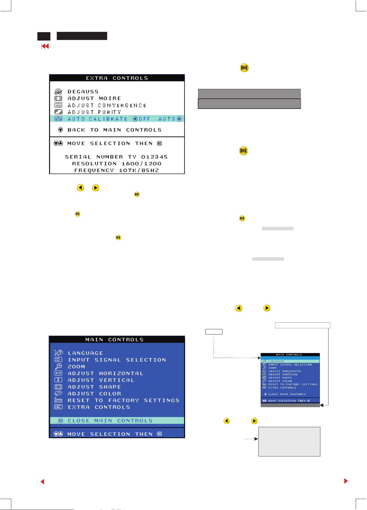
AUTO CALIBRATE
EXTRA CONTROLS is a set of three features, including AUTO
CALIBRATE. Auto Calibrate regularly readjusts the color to its original
value for any of the ADJUST COLOR selections, including USER
PRESET. AUTO CALIBRATE also adjusts the luminance and black
level of the monitor, so that all three items remain at original settings.
This helps extend the useful life of the monitor. The calibration process
takes less than 6 seconds to complete.
1) Press the button on the monitor. The MAIN CONTROLS window
appears.
2) Press the button until EXTRA CONTROLS is highlighted.
8) To adjust the top right purity, press the or button.
9) When the top right purity is adjusted, press the button to
highlight BOTTOM LEFT.
10) To adjust the bottom left purity, press the or
button.
11) When the bottom left purity is adjusted, press the button to
highlight BOTTOM RIGHT.
Back
3) Press the button. The EXTRA CONTROLS window appears.
DEGAUSS will be highlighted.
4) Press the button until AUTO CALIBRATE is highlighted.
Forward
Page 17
16
201P GS3 CM25
Go to cover page
OSD Adjustments (Continued)
To lock (disable) OSD function:
- Press OSD button " " for over 15 seconds to lock the OSD function.
Release it, then OSD comes on the screen as below.
ATTENTION
CONTROL MENU IS LOCKED
To unlock (enable) OSD function:
- Press OSD button " " for over 10 seconds again to unlock the
OSD function.
Release it, then OSD comes on the screen as below.
5) Press the or button to select OFF or AUTO.
6) When the selection is made, press the button to confirm your
selection and return to the MAIN CONTROLS window. CLOSE
MAIN WINDOW will be highlighted.
7) Press the button to exit the MAIN CONTROLS window.
Smart Help
After returning to MAIN CONTROLS...
...toexit completely, press the button.
CLOSE MAIN CONTROLS
Disable/Enable all the WARNING SIGNAL &
Access Service mode (burn in mode) :
To disable all the WARNING SIGNAL :
- Disconnect the Interface cable of the monitor (Monitor is ON.).
- Press OSD button " " for over 15 seconds to disable all the
WARNING SIGNAL. Then release the "OSD" button.
- If it is successful, then the signal " "disappeared to enter
power saving-off mode.
To enable all the WARNING SIGNAL :
-After disconnect the Interface cable of the monitor,then Monitor is powered ON.
- If it is successful, the signal " " comes on the screen again later.
NO SIGNAL INPUT
NO SIGNAL INPUT
Access Service Mode & Burn in mode
Firstly, get into Factory Adjustment Mode.
Push LEFT & RIGHT buttons at the same time for
over 15 seconds and release them.
The factory message appears at the bottom of the
main OSD menu. (for example :Gs3 201P V3.07 000107 ;
00195 is
M.T.B.F. in HOUR unit)
Back
00195
GS3 201P V3.07 000107
- Disconnect the Interface cable of the monitor.
-
Push LEFT & RIGHT buttons at the same time,then power ON.
- If it is successful, the signal " "
comes on the screen later.
(Background is white.).
Leave " MODE" :
burn in
.
Reconnect the interface cable to PC,
then the " MODE" disappear.
burn in
SERVICE MODE
SERIAL NO: TY 123456
HOURS : 00021
FACTORY VER 1.01 990706
Forward
Page 18
Warning and Notes
201P GS3 CM25
Go to cover page
17
1. Safety Instructions for Repairs
1.1 Safety regulations require that during a repair:
- The set should be connected to the mains via an isolating
transformer.
- Safety components, indicated by the symbol , should be
replaced by components identical to the original ones.
- When replacing the CRT, safety goggles must be worn.
1.2 Safety regulations require also that after a repair:
- The set should be returned in its original condition.
- The cabinet should be checked for defects to avoid touching,
by the customer, of inner parts.
- The insulation of the mains lead should be checked for
external damage.
- The mains lead strain relief should be checked on its
function.
- The cable form and EHT cable are routed correctly and fixed
with the mounted cable clamps in order to avoid touching of
the CRT, hot components or heat sinks.
* Thermally loaded solder joints should be checked and
resoldered where necessary. This includes components like
LOT, the line output transistor, fly-back capacitor.
2. Maintenance Instructions
and on the picture tube panel.
3.4 Never replace modules or other components while the unit is
switched on.
3.5 When making settings, use plastic rather than metal tools.
This will prevent any short-circuit and the danger of a circuit
becomes unstable.
3.6 After repair the wiring should be fastened once more in the cable
clamps for this purpose.
3.7 Together with the deflection unit the picture tube is used as an
integrated unit. Adjustment of this unit during repair is therefore
not recommended.
4. Notes
The semiconductors indicated in the circuit diagram(s) and in the
parts lists are completely interchangeable per position with the
semiconductors in the unit, irrespective of the type indication on
these semiconductors.
It is recommended to have a maintenance inspection carried out
periodically by a qualified service employee. The interval depends on
the usage conditions.
- During the maintenance inspection the above mentioned "safety
instructions for repair" should be carried out The power supply and
deflection circuitry on the chassis, the CRT panel and the neck of
the CRT should be cleaned.
When cleaning the monitor on the outside:
- Always disconnect the monitor from the mains.
- Always use a damp AND NOT WET lint-free cloth.
- To clean the screen, apply a household glass cleaner to a cloth and
then wipe the screen.
- Do not use solvents or abrasives on the monitor.
It might discolour the cabinet and/or affect the anti glare treatment
on your screen.
3. Warnings
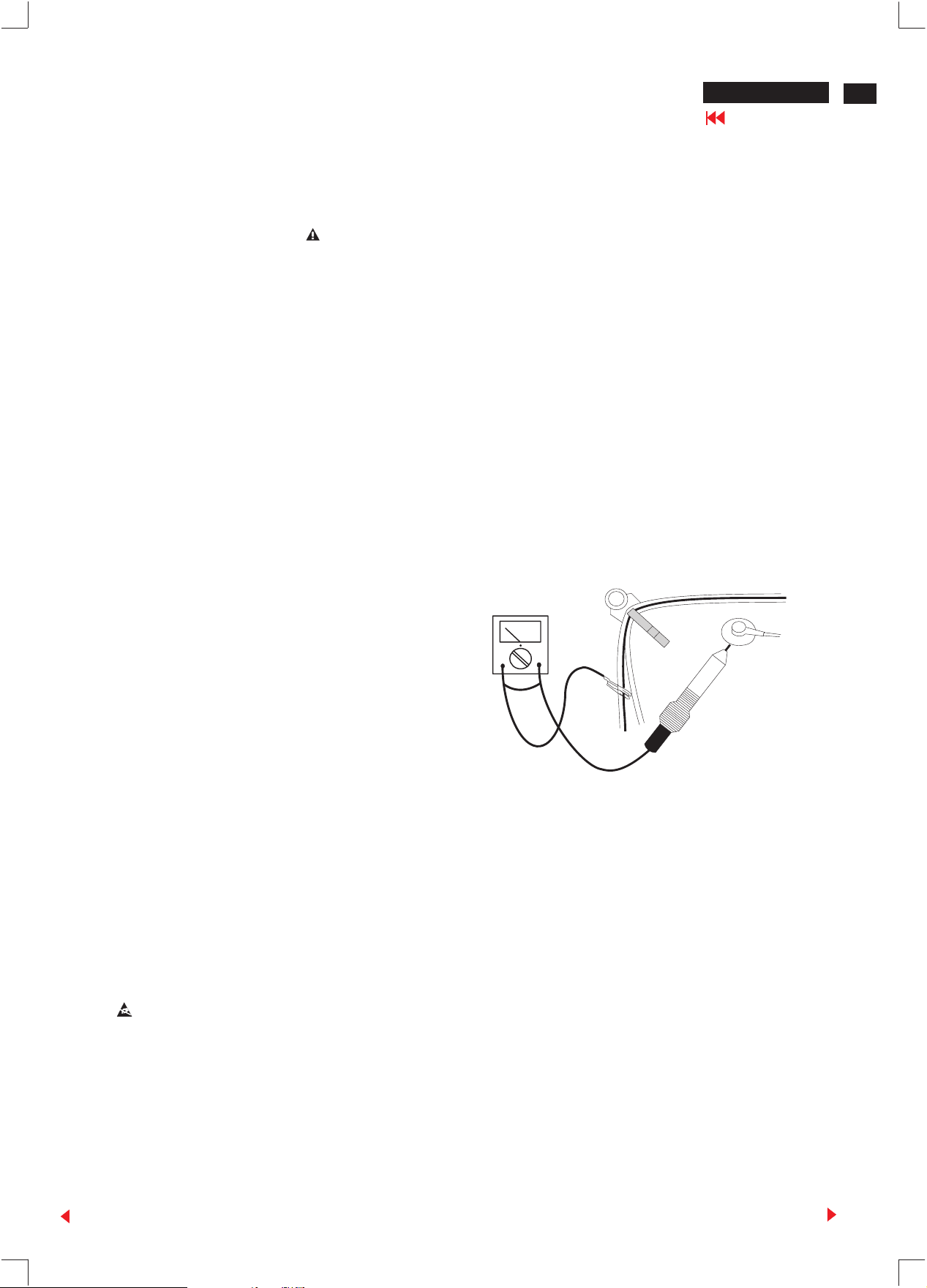
3.1 In order to prevent damage to ICs and transistors, all high-
voltage flash-overs must be avoided. In order to prevent damage to
the picture tube, the method shown in Fig 3.1 should be used to
discharge the picture tube. Use a high-voltage probe and a
multimeter (position DC-V). Discharge until the meter reading is 0V
(after approx 30s).
3.2ESD
V
Fig. 3.1
All ICs and many other semiconductors are sensitive to electrostatic
discharges (ESD). Careless handling during repair can drastically
shorten the life. Make sure that during repair you are connected by a
pulse band with resistance to the same potential as the earth of the
unit. Keep components and tools also at this same potential.
3.3 Be careful when taking measurements in the high-voltage section
Back
Forward
Page 19
18
201P GS3 CM25
Go to cover page
DDC DATA
************************************************************
MITSUBISHI GS3.chk
************************************************************
Vendor/Product Identification
ID Manufacturer Name : PHL
ID Product Code : 221A(HEX.)
ID Serial Number : 123456(DEC.)
Week of Manufacture : 39
Year of Manufacture : 1999
EDID Version, Revision
Version : 1
Revision : 2
Basic Display Parameters/Features
Video Input Definition : Analog Video Input
Maximum H Image Size : 41 cm
Maximum V Image Size : 30 cm
Display Transfer Characteristic: 2.72
(gamma)
Feature Support (DPMS) : Standby
Display Type : RGB color display
Color Characteristics
Red X coordinate : 0.622
Red Y coordinate : 0.339
Green X coordinate : 0.279
Green Y coordinate : 0.6
Blue X coordinate : 0.149
Blue Y coordinate : 0.072
White X coordinate : 0.283
White Y coordinate : 0.297
Established Timings
Established Timings I : 720 x 400 @70Hz (VGA,IBM)
Established timings II : 800 x 600 @72Hz (VESA)
Manufacturer's timings :
Standard Timing Identification #1
Horizontal active pixels : 1920
Aspect Ratio : 4:3
Refresh Rate : 60
Standard Timing Identification #2
Horizontal active pixels : 1792
Aspect Ratio : 4:3
Refresh Rate : 75
Standard Timing Identification #3
Horizontal active pixels : 1600
Aspect Ratio : 4:3
Refresh Rate : 75
Standard Timing Identification #4
Horizontal active pixels : 1280
Aspect Ratio : 5:4
Refresh Rate : 85
Standard Timing Identification #5
Horizontal active pixels : 1280
Aspect Ratio : 5:4
Refresh Rate : 60
0.700V/0.000V (0.70Vpp)
without Blank-to-Black Setup
Separate Sync
Composite Sync
without Sync on Green
no Serration required
Suspend
Active Off
720 x 400 @88Hz (XGA2,IBM)
640 x 480 @60Hz (VGA,IBM)
640 x 480 @72Hz (VESA)
640 x 480 @75Hz (VESA)
800 x 600 @60Hz (VESA)
800 x 600 @75Hz (VESA)
832 x 624 @75Hz (Mac II)
1024 x 768 @60Hz (VESA)
1024 x 768 @70Hz (VESA)
1024 x 768 @75Hz (VESA)
1280 x 1024 @75Hz (VESA)
1152 x 870 @75Hz (Mac II)
Standard Timing Identification #6
Detailed Timing #1
Monitor Descriptor #2
Monitor Descriptor #3
Monitor Descriptor #4
Extension Flag : 0
Check
sum
104: 30 105:39 106:42 107:0a 108:00 109:00 110:00 111: fd
112: 00 113:32 114:a0 115:1e 116:60 117:14 118:00 119:0a
120: 20 121:20 122:20 123:20 124:20 125:20 126:00 127:21
Horizontal active pixels : 1024
Aspect Ratio : 4:3
Refresh Rate : 85
Pixel Clock (MHz) : 319.92
H Active (pixels) : 2048
H Blanking (pixels) : 608
V Active (lines) : 1536
V Blanking (lines) : 70
H Sync Offset (F Porch) (pixels): 64
H Sync Pulse Width (pixels) : 216
V Sync Offset (F Porch) (lines): 1
V Sync Pulse Width (lines) : 3
H Image Size (mm) : 392
V Image Size (mm) : 294
H Border (pixels) : 0
V Border (lines) : 0
Flags : Non-interlaced
Serial Number : TY 123456
Monitor Name : Philips 201P
Min. Vt rate Hz : 50
Max. Vt rate Hz : 160
Min. Horiz. rate kHz : 30
Max.Horiz. rate kHz : 121
Max. Supported Pixel : Not specified
* ***********************************
EDID data for Mitsubishi CRT
*************************************
0: 0 1: ff 2:ff 3:ff 4:ff 5:ff 6:ff 7:00
8: 41 9:0 c 10:6b 11:99 12:39 13:30 14:00 15:00
0: 00 1: ff 2: ff 3: ff 4: ff 5: ff 6: ff 7: 00
16: 19 17:09 18:01 19:02 20:2c 21:24 22:1b 23:b4
8: 41 9: 0c 10: 1a 11: 22 12: 40 13: e2 14: 01 15: 00
24: e8 25:90 26:22 27:a2 28:55 29:49 30:9b 31:27
16: 27 17: 09 18: 01 19: 02 20: 6c 21: 29 22: 1e 23: ac
32: 11 33:48 34:4f 35:a0 36:43 37:00 38:31 39:59
24: e9 25: 7a 26: 68 27: 9f 28: 56 29: 47 30: 99 31: 26
40: 45 41:59 42: 61 43:59 44:81 45:99 46:a9 47:4f
32: 12 33: 48 34: 4c 35: ff 36: ff 37: 80 38: d1 39: 4f
48: 01 49:01 50:01 51:01 52:01 53:01 54:1a 55:4f
40: c1 41: 4f 42: a9 43: 4f 44: 81 45: 99 46: 81 47: 80
56: 40 57:30 58:62 59:b0 60:32 61:40 62:40 63:c0
48: 61 49: 59 50: 45 51: 59 52: a9 53: 59 54: f8 55: 7c
64: 13 65:00 66:68 67:0e 68:11 69:00 70:00 71:1e
72: 00 73:00 74:00 75:ff 76:00 77:20 78:54 79:59
56: 00 57: 60 58: 82 59: 00 60: 46 61: 60 62: 40 63: d8
80: 20 81:31 82:32 83:33 84:34 85:35 86:36 87:0a
64: 13 65: 00 66: 88 67: 26 68: 11 69: 00 70: 00 71: 1e
88: 20 89:20 90:00 91:00 92:00 93:fc 94:00 95: 50
72: 00 73: 00 74: 00 75: ff 76: 00 77: 20 78: 54 79: 59
96: 48 97:49 98:4c 99:49 100:50 101:53 102:20 103:31
80: 20 81: 20 82: 31 83: 32 84: 33 85: 34 86: 35 87: 36
Normal Display, No stereo
Digital Seperate Sync
Positive V Sync
Positive H Sync
: 81(hex)
88: 0a 89: 20 90: 00 91: 00 92: 00 93: fc 94: 00 95: 50
96: 48 97: 49 98: 4c 99: 49 100: 50 101: 53 102: 20 103: 32
104: 30 105: 31 106: 50 107: 0a 108: 00 109: 00 110: 00 111: fd
112: 00 113: 32 114: a0 115: 1e 116: 79 117: ff 118: 00 119: 0a
120: 20 121: 20 122: 20 123: 20 124: 20 125: 20 126: 00 127: 81
Back
Forward
Page 20
DDC Instructions
201P GS3 CM25
Go to cover page
19
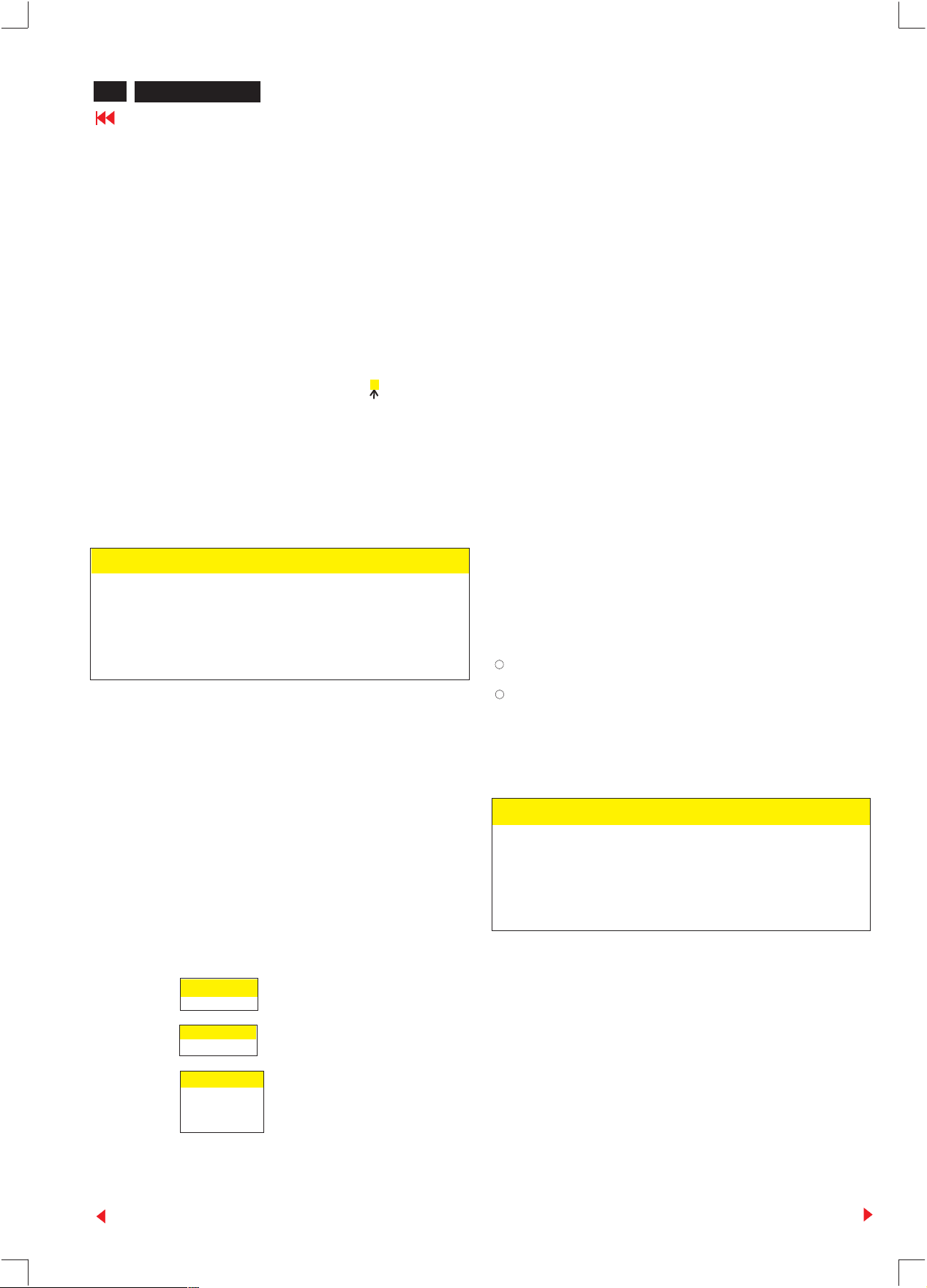
There are two chips (IC) to store the serial number of monitor
as below.
DDC IC (with EDID data)
OSD IC (EEPROM)
To write the serial number of monitor to DDC IC and OSD IC
simultaneously.
Please follow the indications as below.
- Access the factory mode of monitor.
- Execute DDCV2A F0.EXE
- Follow DDC instructions to write serial number to DDC IC and OSD
IC.
- Turn off monitor (leave factory mode).
- Press OSD button, select MONITOR STATUS, verify the updated
serial number of monitor.
To access factory mode:
-
Turn off monitor (don't turn off PC)
- Hold " " and " " simultaneously on the front control panel,
then press " ", wait till the OSD menu with characters "
factory mode (below OSD menu)" come on the screen of monitor
as shown in Fig. 1 .
- If OSD menu disappears on the screen of monitor, press " "
again (anytime), then the OSD menu comes on the screen again.
- using " , " : to select OSD menu.
" " : to increase or decrease the setting.
,
- Using " " to confirm the selection.
Additional information :
Additional information about DDC (Display Data Channel)
may be obtained from Video Electronics Standards
Association (VESA).
Extended Display Identification (EDID) information may be
also be obtained from VESA.
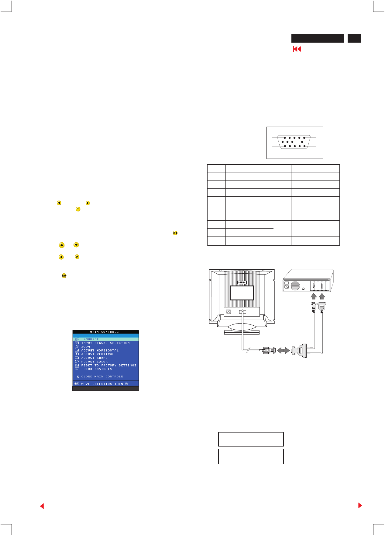
Pin assignment
The 15-pin D-sub connector (male) of the signal cable (3 rows)
for DDC feature :
1
6
11
Pin No. Assignment Pin No. Assignment
1 Red video input 9 No pin
2 Green video input 10 Logic ground
3 Blue video input 11 Connected to pin 10
4 Connected to pin 10 12 Serial data line
(SDA)
5 Ground 13 H.sync/H+V
6 Red video ground 14 V. sync (VCLK for
7 Green video ground DDC)
8 Blue video ground 15 Data clock line(SCL)
5
10
15
Connection
(Rear of the monitor)
To leave factory mode
* After alignment of factory mode, turn off monitor (if you do not turn
off monitor, the OSD menu is always at the factory mode), then turn
on monitor again (at this moment, the OSD menu goes back to
user mode).
Fig 1
00195
GS3 201P V3.07 000107
DDC Instructions
This [DDC Module (DDC cable)= 4822 320 12004(=4822 724 27550)]
and
[DDC V2(DDCV2A .EXE) software(3.5" disk)=3138 106 10065 ]
are used for "BU Monitor - Chungli product range" which
incorporates a DDC1/DDC2B function that allows
bi-directional communication between the monitor and
PC system for optimal video configuration.
[January 31 2000, Revision 3.3] ,which upgrades the software and
service information(4822 727 21027 & 4822 727 21038) , is fully
compatible with previous one (DDCV2AF0.E
XE).
To video card
Video cable
DDC data re-programming
1. General
In case the DDC data memory IC, replaced due to a defect the
data contents of this IC have to be re- programmed via a PC.
In case of replacement of the video (or deflection) board it is
advised to re-soldered DDC IC from the old board onto the new
board, in this case the IC dose not need to be re-programmed.
2. DDCV2A.EXE can be used for :
EDID Structure Version/Revision
Version : 1
Revision : 0 (text file)
and
Version : 1
Revision : 2 (.hex file)
To printer port (LTP1)
Back
Forward
Page 21
20
201P GS3 C 25
Go to cover page
M
DDC Instructions (Continued)
DDC Reprogramming Instructions (for
PHILIPS models)
System Requirements
DDC Module (DDC cable), P/N = 4822 320 12004
An Intel 386 (or above) PC or compatible
DOS 6.0 or above
DDCV2A.EXE software
Procedure
Connect DDC Cable between PC and Monitor.
Turn on Monitor and PC.
Access Factory Mode of monitor.
Verify Factory Mode by OSD function of monitor.
Insert diskette in Drive a: Select Run "DDCV2A F0(Zero).EXE"
under DOS or Win. (hit the space bar “once”)
Verify the data and version of DDC application software.
It should be : January 31 2000
Revision 3.3
Press "Enter" at the introduction screen
Menu Configuration:
File R/W Setup Quit
How to write DDC hex files to Monitor
Use arrow keys to highlight "Options" under the Setup menu,
press "Enter"
Tab down to ID Serial Number, use down arrow key to place
the asterisk (*) beside "store in DEC with LSB first". Press
"control/enter" to save.
(Ensure the top asterisk (*) is beside in store in HEX with LSB
first.)
Use arrow keys to highlight "Load EDID" under the file menu,
press "Enter".
Use arrow keys to highlight "PHILIPS\", Press "Enter".
Use arrow keys to highlight "the model list under subdirect",
press "Enter".
Use arrow keys to highlight "Write EDID to EEPROM" under
the R/W menu, press "Enter".
Use arrow keys to highlight "Read from EEPROM" under the
R/W menu, press "Enter".
Use arrow keys to highlight "Edit EDID Code" under the R/W
menu, press "Enter".
Load EDID Write EDID to EEPROM Options
Load txt file (V1.0) Read From EEPROM Barcode format
Save EDID Edit EDID Code
Save txt File Auto Scan
Convert EDID Code
Os shell
Exit
General :
1.How to change drive
Use arrow keys to highlight "Options" under the Setup
menu, press "Enter".
Press "F2", then press "ESC", fill in "A" or "C".
[(If your .HEX files for different Model numbers in drive "A",
then fill in "A").,
(If your .HEX files for different Model numbers in drive "C",
then fill in "C").
Normally, to read DDC data from EEPROM of Monitor is
enough.]
Press "Enter", then press "ESC"
2.
How to select .HEX files for different Model numbers
example:
Use arrow keys to highlight "Load EDID" under the File
menu, press "Enter"
Bring up PHILIPS\ press "Enter"
Verify the ID Serial number on the screen matches the serial
number of the unit.
Verify EDID Structure Version is "Version :2, Revision :1
11
Press "ESC"
12
Use arrow keys to highlight "Quit", Press "Enter".
Menu Configuration:
File R/W Setup Quit
Load EDID Write EDID to EEPROM Options
Load txt file (V1.0) Read From EEPROM Barcode format
Save EDID Edit EDID Code
Save txt File Auto Scan
Convert EDID Code
Os shell
Exit
Bring up ..\
201P GSIII select, press "Enter"
Bring up ..\ at this highlight area, press
00MITS.HEX select for 201P10/00(MITS CRT)ß
ß
"Enter", then go back to last
screen
Back
Forward
Page 22
DDC Instructions (Continued)
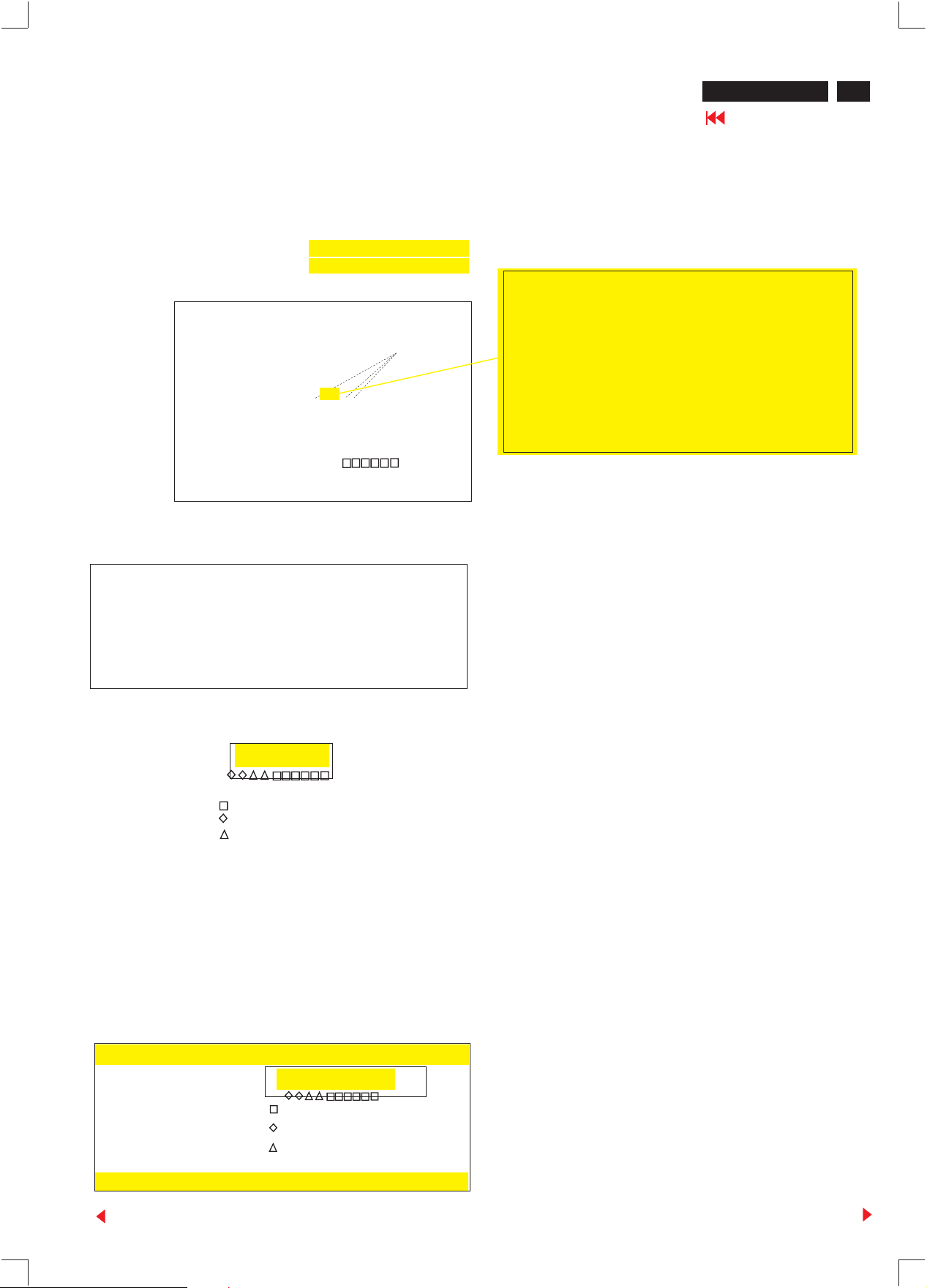
How to change the Year, Week & Serial
number of Monitor [for PHILIPS(BRANDED)
models]
Use arrow keys to highlight "Barcode format", under the Setup menu,
press "Enter".
Bring up : Barcode example : 9925123456
continued: Barcode example : 9925123456
Barcode format : YYWWSSSSSS
----------------------------------------------------------
Barcode format : YYWWSSSSSS
---------------------------------------------------------Manufacture Year : 1999
Manufacture Week : 25
Serial No. : 123456
Serial No. ASCII : _ TY _ _ 123456
================================
EDID [16] Week : 19
EDID [17] Year : 09 [Year-1990]
EDID [12..15] : 0001e240
EDID [77 -89] : TY
data correct ? (Y/N) Y
TY
press "space"
201P GS3 C 25
¬
Fill in 9925123456, press "Enter"
Fill in YYWWSSSSSS, press "Enter"
¬
Factory code for each site is as below.
Brazil H C (48h,43h)
Chungli T Y (54h,59h)
Delta G K(47h,4Bh)
Juarez Y A(59h,41h)
Shenzshen C X(43h,58h)
Suzhou BZ (42h,5Ah)
Szombathely HD (48h,44h)
Fill in "Y", don't press "Enter"
¬
M
Go to cover page
21
There is a description at the lower of the screen for Barcode format as
below.
Barcode format : Y,W,S,X,- (year,week,s/no,ignore,fixed)
Y stands for "year".
W stands for "week".
S stands for "s/no (serial number)".
X stands for "ignore". Allow user to fill in any 'character' or 'numeric'.
- stands for "fixed". User have to fill in Special 'character' or 'numeric'
for "AutoScan" if user fill in '-' at "Barcode format :".
Use arrow keys to highlight "Auto Scan" under the R/W menu, press
"Enter".
Bring up: Auto Scan year, week, serial
Serial Number
Year Code
Week Code
don't care
¬
number can be
changed.
*
(If monitor is not at Factory Mode, access Factory Mode at
this moment.)
Fill in "Barcode data (for instance: 9925123456)" beside AutoScan,
press "Enter".
After 10 seconds around, bring up:
File R/W Setup Quit
Write EDID to EEPROM
Read From EEPROM
Edit EDID Code
Auto Scan
Factory writing ...100% (58) (f8) (7f) (12).
*
Back
Press "ESC" "ESC", return to R/W menu.
Select "Edit EDID code", press "Enter".
Verify "ID Serial No.".............
Turn off monitor, then turn on monitor again.
Press OSD button, select "MONITOR STATUS", press OSD button
again.
Verify "SERIALNO".
(Leave OSD function).
Use arrow keys to highlight "QUIT", press "Enter".
Forward
Page 23
201P GS3 C 25
22
M
DDC Instructions (Continued)
Go to cover page
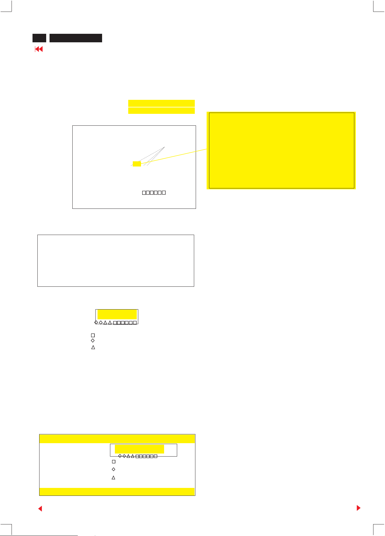
How to change the Year, Week & Serial
number of Monitor [for PHILIPS(PCEC)
models]
Use arrow keys to highlight "Barcode format", under the Setup menu,
press "Enter".
Bring up : Barcode example : 993412345678
continued: Barcode example : 993412345678
Barcode format : YYWWSSSSSSSS
----------------------------------------------------------
Barcode format : YYWWSSSSSSSS
---------------------------------------------------------Manufacture Year : 1999
Manufacture Week : 34
Serial No. : 12345678
Serial No. ASCII : _ TY _ _ 12345678
================================
EDID [16] Week : 22
EDID [17] Year : 09 [Year-1990]
EDID [12..15] : 00bc614e
EDID [77 -89] : TY
data correct ? (Y/N) Y
TY
press "space"
¬
Fill in 993412345678, press "Enter"
Fill in YYWWSSSSSSSS, press "Enter"
¬
Factory code for each site is as below.
Brazil H C (48h,43h)
Chungli T Y (54h,59h)
Delta G K(47h,4Bh)
Juarez Y A(59h,41h)
Shenzshen C X(43h,58h)
Suzhou BZ (42h,5Ah)
Szombathely HD (48h,44h)
Fill in "Y", don't press "Enter"
¬
There is a description at the lower of the screen for Barcode format as
below.
Barcode format : Y,W,S,X,- (year,week,s/no,ignore,fixed)
Y stands for "year".
W stands for "week".
S stands for "s/no (serial number)".
X stands for "ignore". Allow user to fill in any 'character' or 'numeric'.
- stands for "fixed". User have to fill in Special 'character' or 'numeric'
for "AutoScan" if user fill in '-' at "Barcode format :".
Use arrow keys to highlight "Auto Scan" under the R/W menu, press
"Enter".
Bring up: Auto Scan year, week, serial
Serial Number
Year Code
Week Code
don't care
¬
number can be
changed.
*
(If monitor is not at Factory Mode, access Factory Mode at
this moment.)
Fill in "Barcode data (for instance: 993412345678)" beside AutoScan,
press "Enter".
After 10 seconds around, bring up:
File R/W Setup Quit
Write EDID to EEPROM
Read From EEPROM
Edit EDID Code
Auto Scan
Factory writing ...100% (58) (f8) (7f) (12).
*
Back
Press "ESC" "ESC", return to R/W menu.
Select "Edit EDID code", press "Enter".
Verify "ID Serial No.".............
Turn off monitor, then turn on monitor again.
Press OSD button, select "MONITOR STATUS", press OSD button
again.
Verify "SERIALNO".
(Leave OSD function).
Use arrow keys to highlight "QUIT", press "Enter".
Forward
Page 24
Electrical Adjustments
201P GS3 CM25
Go to cover page
23
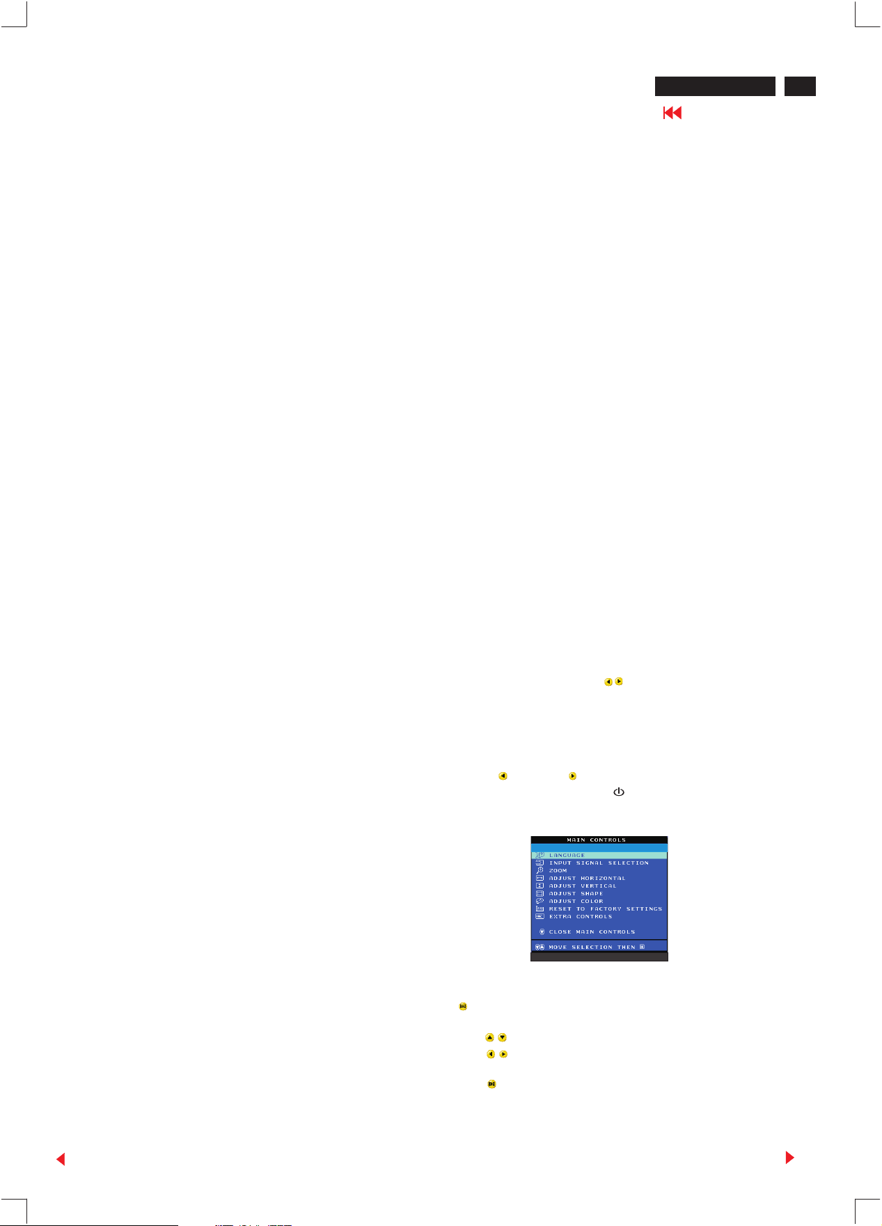
0. General
When carry-out the electrical settings in many cases a video
signal must be applied to the monitor. A computer with :
- ATI GPT-1600 (4822 397 10065), Mach 64 (up to 107kHz)
are used as the video signal source. The signal patterns are
selected from the "service test software" package, see user
guide 4822 727 21046 (GPT-1600).
0.1 This monitor has 35 factory-preset modes as below
.
31.469 KHz/70.087 Hz, 640 X 350
31.469 KHz/59.941 Hz, 640 X 480
31.468 KHz/70.084 Hz, 720 X 400
37.5 KHz/75 Hz, 640 X 480
37.861 KHz/72.810 Hz, 640 X 480
37.861 KHz/85.081 Hz, 640 X 350
37.879 KHz/60.317 Hz, 800 X 600
37.927 KHz/85.039 Hz, 720 X 400
43.269 KHz/85.008 Hz, 640 X 480
46.875 KHz/75.000 Hz, 800 X 600
48.077 KHz/72.188 Hz, 800 X 600
48.363 KHz/60.004Hz, 1024X 768
49.722 KHz/74.546Hz, 832 X 624
50.628 KHz/100.10 Hz, 640 X 480
53.674 KHz/85.061 Hz, 800 X 600
56.476 KHz/70.069 Hz,1024X 768
60.000 KHz/60.000 Hz,1280 X 960
60.023KHz/75.029Hz, 1024 X 768
63.923 KHz/100.00 Hz, 800 X 600
63.981KHz/60.020Hz, 1280 X 1024
67.500 KHz/75.00Hz, 1152 X 864
68.677KHz/84.997Hz, 1024 X 768
68.681KHz/74.979Hz, 1152 X 870
71.809KHz/76.15 Hz, 1152 X 900
75.000KHz/60.000 Hz, 1600 X 1200
79.976KHz/75.024 Hz, 1280 X 1024
81.250 KHz/65.000 Hz, 1600 X 1200
83.640 KHz/59.999 Hz, 1792 X 1344
85.938 KHz/85.002 Hz, 1280 X 960
86.333 KHz/59.995 Hz, 1856X 1392
87.500 KHz/70.000 Hz, 1600 X 1200
90.000 KHz/60.000 Hz, 1920 X 1440
91.146 KHz/85.024 Hz, 1280 X 1024
93.750 KHz/75.000Hz, 1600 X 1200
106.250KHz/85.00 Hz, 1600 X 1200
106.270KHz/74.997Hz, 1792 X 1344
95.820 KHz/60.000 Hz, 2048 X 1536
112.50 KHz/75.000 Hz, 1920 X 1440
120.45 KHz/75.000 Hz, 2048 X 1536
- Connect a "high-voltage voltmeter" between the highvoltage connection of the picture tube and earth.
- Turn on the power.
- Set the EHT trimming potentiometer 3698 so that the "highvoltage voltmeter" reads 27.0 kV +/- 0.2 kV .
- Turn off the power.
- Remove the "high-voltage voltmeter" from the picture tube.
- Turn on the power again.
3. Monitor the following auxiliary voltages.
SOURCE ACROSS C2362 + 8.0V +/- 0.5 VDC
SOURCE ACROSS C2143 + 5.0V +/- 0.5 VDC
SOURCE ACROSS C2157 - 13.0V +/- 0.5VDC.
SOURCE ACROSS C2361 + 12.0V +/- 0.5 VDC
SOURCE ACROSS C2172 + 13.0V +/- 0.5VDC.
SOURCE ACROSS C2134 + 15.0V +/- 1.0 VDC
SOURCE ACROSS C2156 - 6.4 V+/- 0.2VDC.
SOURCE ACROSS C2137 - 15.5V +/- 1.0 VDC
SOURCE ACROSS C2152 + 193.0V +/- 1.5VDC.
SOURCE ACROSS D6140 “+“ 6.3V +/- 0.5 VDC
SOURCE ACROSS C2154 + 79.0 V +/- 0.2VDC.
SOURCE ACROSS C2131 + 210.0V +/- 1.5 VDC
SOURCE ACROSS C2133 + 82.7V +/- 2.0 VDC
4. General conditions for alignment
4.1 During all alignments, supply a distortion free AC mains
voltage to set via an isolating transformer with low internal
impedance.
4.2 Align in pre-warmed condition, at least 30 minutes warmup with nominal picture brightness.
4.3 Purity, geometry and subsequent alignments should be
carried out in magnetic cage with correct magnetic field.
Northern hemisphere : H=0, V=450+/-50 mG, Z=0
Southern hemisphere : H=0, V=-520+/-50 mG, Z=0
Equatorial Support : H=0, V=0 mG, Z=0
0.2 With normal VGA card:
If not using the ATI card during repair or alignment, The
service engineer also can use this service test software
adapting with normal standard VGA adaptor and using
standard VGA mode 640 x 480, 31.5 kHz/60 Hz (only) as
signal source.
0.3 AC/DC Measurement:
The measurements for AC waveform and DC figure is based
on 640 x 480 31.5 kHz/60 Hz resolution mode with test
pattern "gray scale".
Power input: 110V AC
1. B+ supply voltage (3157) 210Vdc
- Apply a video signal in the 1024 x 768 with 68.7 kHz/85Hz
mode.
- Select the "cross-hatch" pattern.
- Set the brightness control and the contrast control to the
minimum position.
- Pre-set trimming potentiometer 3157(B+) and 3698(EHT)
in mid-position.
- Set Vg2 (screen) to fully Counter-clockwise (zero
beamcurrent).
- Connect a dc voltmeter between the joint of capacitor 2131
and ground (common ground).
- Set the B+ trimming potentiometer 3157 so that the reading
on the dc voltmeter is 210 V +/- 0.5 Vdc.
2. High-voltage EHT (3698)
- Apply a video signal in the 1024 x 768 with 68.7 kHz/85Hz
mode.
- Select the "cross-hatch" pattern.
- Set the brightness control and the contrast control to the
minimum position.
- Turn off the power.
4.4 All voltages are to be measured or applied with respect to
ground.
Note: Do not use heatsink as ground.
4.5 Adjust function controls " " to center position except
for contrast control which should be set to MAX.
5. To access factory mode:
- Turn off monitor (don't turn off PC)
- Press " " and " " simultaneously on the front
control panel, then press " ",wait till the OSD menu
with characters " factory mode (below OSD menu)" come
on the screen of monitor.
00195
GS3 201P V3.07 000107
- If OSD menu disappears on the screen of monitor, press
" " again (anytime), then the OSD menu comes on the
screen again.
- using " " : to select OSD menu.
: to increase or decrease the setting.
- Using " " to confirm the selection.
Back
Forward
Page 25
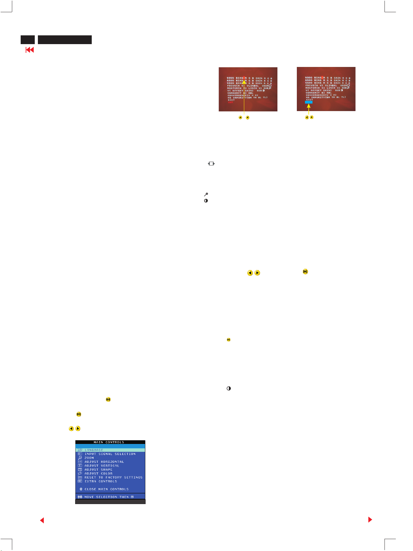
24
201P GS3 CM25
Electrical Adjustments (Continued)
Go to cover page
6 To leave factory mode
* After alignment of factory mode, turn off monitor (if you do
not turn off monitor, the OSD menu is always at the factory
mode), then turn on monitor again (at this moment, the
OSD menu goes back to user mode).
.
107
TIMER Set OSD display time.
7. Alignment of Vg2 cut-off point, white tracking (OSD
control)
Equipment : 1. Video Test Generator-801GC (Quantum
Data)
2. Color-analyzer (Minolta CA-100)
VG2 [(screen), at the bottom of the L.O.T.].
* Apply a video signal in the 1024 x 768 with 68.7 kHz/85 Hz
mode,
select the "full white pattern" (sizes 392 x 294 mm).
* Use color-analyzer (Minolta CA-100) to adjust cutoff and
white uniformity.
OSD R/G/B cut-off and R/G/B gain can be accessed, with
initial data:
°
9300 K
R cutoff = 30%, R gain = 70% (I C)
G cutoff = 30%, G gain = 70% (I C)
B cutoff = 30%, B gain = 70% (I C)
°
6500 K
R cutoff = 30%, R gain = 70% (I C)
G cutoff = 30%, G gain = 70% (I C)
B cutoff = 30%, B gain = 70% (I C)
°
5500 K
R cutoff = 30%, R gain = 70% (I C)
G cutoff = 30%, G gain = 70% (I C)
B cutoff = 30%, B gain = 70% (I C)
Brightness = 50%, Sub-Contrast = 90%, ABL = 50% (I C)
2
2
2
2
2
2
2
2
2
2
Step 1: To select the character "FACTORY MODE" as shown
in Fig. 2.1, press " " to access the OSD menu for
R/G/B gain & cutoff as shown in Fig. 2.2.
Step 2: Press " " for function selection as shown in Fig
2.3.
Step 3: Use " " to increase or decrease the value as
shown in Fig. 2.3.
00195
Fig. 2.2
BIASRGB:R(red) G(green) B(blue) cutoff
GAINRGB:R(red) G(green) B(blue) gain
V FOCUS : Vertical Focus
H FOCUS : Horizontal Focus
VLIN BAL : Vertical Linearity Balance
USER : Horizontal size range
RASTER H: Horizontal raster Shift
RASTER V: Vertical raster Shift
HLIN : Horizontal Linearity
V LIN : Vertical Linearity
SUB : Zoom Control range
SUB : Sub Contrast
V OFFSET : Vertical offset
V GAIN : Vertical Gain
ABL : Auto Beam Limit
T CORNER: Corner Correction of TOP
B CORNER: Corner Correction of BOTTOM
CONVERGENCE(V H R):CONVERGENCE Correction of Vertical ,
NS IMPURITY(BR TR BL TL):NS IMPURITY Correction of BOTTOM
Horizontal,Corner (RESERVED).
TOP BOTTOM LEFT,
RIGHT,
TOP LEFT.
RIGHT,
Fig. 2.3
After pressing " " ,then Press " "
7.1 Connect the video input, set brightness control at 50%
and contrast at minimum position (OSD), Vg2 at Minimum
(counter clockwise, and ABL (OSD) at 50% position.
Slowly increase Vg2 voltage until light output is at
0.1 Ft-L +/- 0.01Ft-L (Y=0.1 Ft-L, on the screen of CA-
100).
7.2 (The screen of monitor is dark now)
: Press " " to show the OSD menu as shown in Fig. 2.1.
: Select the character "FACTORY MODE" to access the
R/G/B adjustment as shown in Fig. 2.2 and Fig. 2.3.
: Adjust the cutoff of R/G/B to get 9300K
(x=0.283 +/- 0.015, y=0.298 +/- 0.015), and brightness
output at 0.07 +/- 0.01 Ft-L (Y=0.07Ft-L).
7.3 : Press " " to set contrast at maximum (100%).
: Adjust gain of R/G/B to get 9300K
(x=0.283 +/- 0.015, y=0.298 +/-0.015, don't care about
the Y value)
7.4 Apply a small white square 10 x 10 cm pattern, brightness
set to center (50%), and contrast at maximum (100%),
adjust Sub-contrast control (OSD) to reach 32 +/- 2 Ft-L.
7.5 Apply full white pattern at 9300K, adjust ABL (OSD) to
reach 32+/- 2 Ft-L (contrast at maximum 100%,
brightness at center 50%).
Back
Fig.2.1
GS3 201P V3.07 000107
Forward
Page 26
Electrical Adjustments (Continued)
7.6 : Select the 6500K colour temperature as shown in Fig.
2.2.
: Adjust the R/G/B cutoff and R/G/B gain as shown in
procedure 7.2~7.3 to get
R/G/B cutoff x= 0.313 +/- 0.015
y= 0.329 +/- 0.015
R/G/B gain x= 0.313 +/- 0.015
y= 0.329 +/- 0.015
Y= 28 +/- 2 Ft-L(Adjust Sub-contrast
control (OSD))
7.7 : Select the 5500K colour temperature as shown in Fig.
2.2.
: Adjust the R/G/B cutoff and R/G/B gain as shown in
procedure 7.2~7.3 to get
R/G/B cutoff x= 0.332 +/- 0.015
y= 0.347 +/- 0.015
R/G/B gain x= 0.332 +/- 0.015
y= 0.347 +/- 0.015
Y= 25 +/- 2 Ft-L(Adjust Sub-contrast
control (OSD))
8. Picture geometry setting (factory pre-set modes)
201P GS3 CM25
Go to cover page
9. Focus adjustment
: Apply a video signal in the 1024 x 768 with 68.7 kHz/85 Hz
mode
: Select " @ " pattern.
: Set the brightness at center (50%) and the contrast to 22
FL.
: Adjust focus potentiometers (top of L.O.T.) Focus 1 for
horizontal focus and Focus 2 for vertical focus so that the
picture at 2/3 of the diagonal lines (from center to four
corners) of the displayed screen is as sharp as possible.
10. Loading DDC code
into the DDC IC by EEPROM writer or equivalent method.
a: Service DDC Kit
DDC Module (DDC cable), Part number = 4822 320 12004
DDCV2A.EXE software (3.5" disk), Part number = 3138
106 10065
b: Please refer to Service information 4822 727 21027(4822
727 21038) for using the Service DDC Kit.
The DDC HEX data should be written
25
- Apply a video signal with cross-hatch pattern.
- Apply a video signal in the 1024 x 768 with 68.7 kHz/85 Hz
mode.
- Set brightness and contrast controls to their center positions
(OSD control).
8.1 Horizontal geometry (OSD control)
- Adjust the H-width to 392 mm
- Adjust the H-phase to center position.
8.2 Vertical geometry (OSD control)
- Adjust vertical size to 294 mm
- Adjust V-phase to center position.
8.3 Trapezoid distortion (OSD control)
- Adjust the trapezoid to get optimal vertical lines.
8.4 Pincushion (OSD control)
- Adjust the pincushion to get optimal vertical line.
8.5 Parallelogram (OSD control)
- Adjust parallelogram so that vertical lines are vertical or
symmetrically about the center vertical axis.
8.6 Unbalance-pin (OSD control)
- Adjust the unbalance-pin so that that vertical border lines
are aligned symmetrically.
8.7 Rotation (OSD control)
- Adjust picture so that vertical tilt is less than +/- 0.5mm.
8.8 Top/Bottom corner(control)
- Adjust the top/bottom corner control to get optimum corner
geometry.
8.9 Store the preset results by selecting the "exit" (OSD
control).
8.10 Repeat the procedure 8.1 to 8.9 until all the preset
timings have been adjusted completely
Back
Forward
Page 27
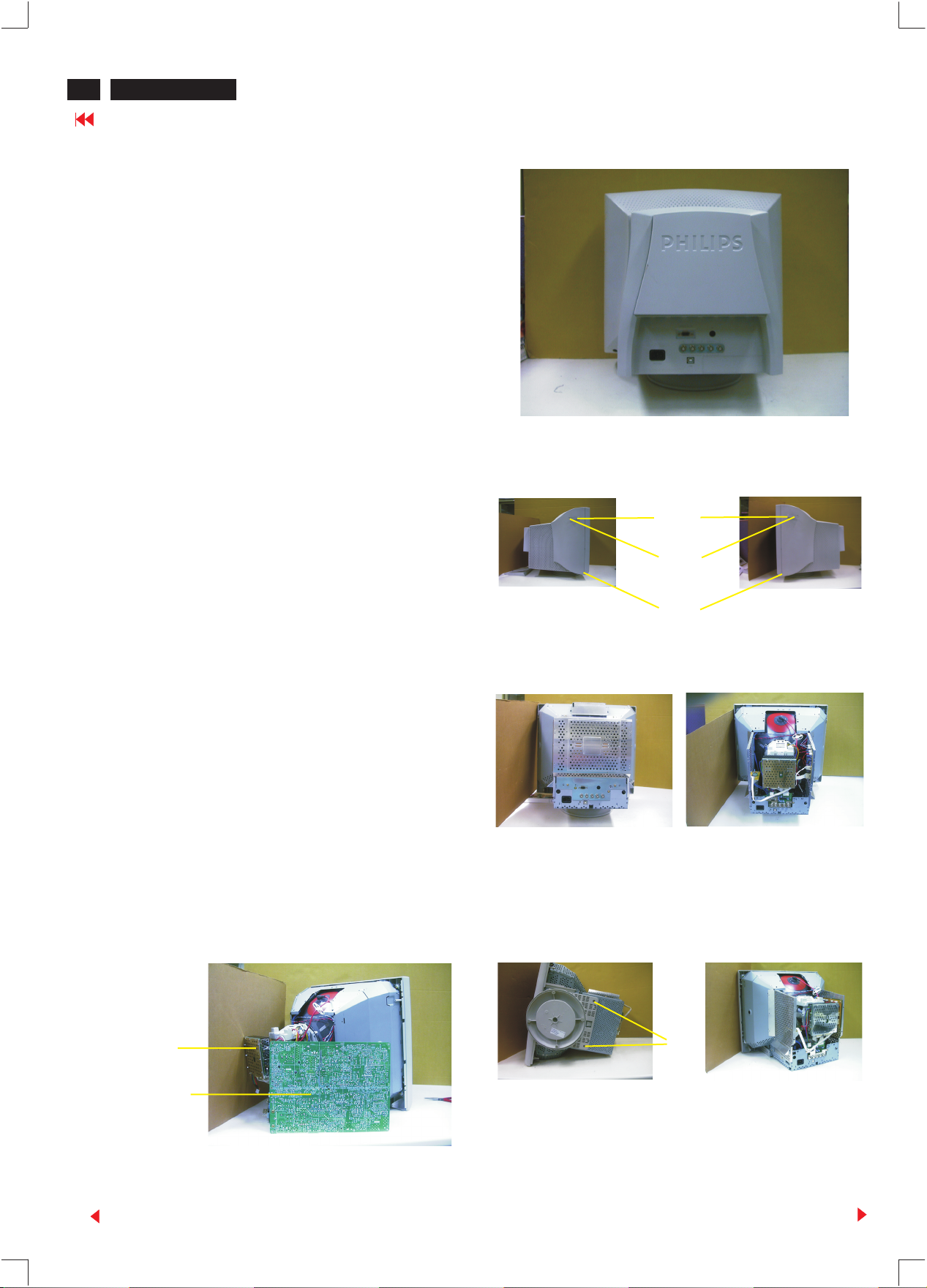
26
201P GS3 C 25
M
Mechnical Instructions
Go to cover page
0. Location of the panel
0.1 Main panel (1160)
0.2 Video panel (1162)
1. General
To be able to perform measurements and repairs on the "circuit
boards", the monitor should be placed in Service Position (fig. 1) first:
Howtoremovethebackcoverofmonitor:
There are 2 screws in the lid [1 screw are at the right side of the
monitor, The other 1 screw are at the left side of the monitor],to fix the
front cabinet and back cover of the monitor.
Step 1: To open the lid at the right-upper side and 1 right-
downer side of the monitor.(FIG.3)
Step 2: To open the lid at the left-upper side and left-
downer side of the monitor.(FIG.4)
Step 3: To remove the back cover, you can see FIG.5
Step 4: To remove the16 screws on the metal shield, and remove the
metal shield, you can see FIG.6.
Chassis :
- After remove the back cover & metal shield, you can see the inside
of the monitor as Fig. 6.
- To remove 16 screws for service position as Fig. 5 to Fig. 8.
- Include remove bottom plate screw, then slide out chassis board
and disconnect metal shield.
Video panel :
- After remove the metal frame (Fig. 5), to remove the metal shield on
rear side of Video panel for measurement.
Main panel :
After remove the metal frame.
- To cut out cable tie and disconnect "video panel"
- To disconnect EHT cable
- To disconnect ground wire(1703) of video board.
- To disconnect M1311(4pin) to control panel.
- To disconnect M1501(4pin) yoke connector.
- To disconnect M1131(2pin) degaussing coil
- To slide out Main panel as Fig. 1.
screw in
1screw in
Fig. 3
Fig. 2
screws
lids
screws
Fig. 4
Service position :
To get service position as Fig. 1 through Fig. 2 to Fig. 8.
2. Repair instructions
After the service position was obtained, all the panel's copper track
side could be accessed.
1162
1160
Fig. 1 Service Position
Fig. 5
Fig. 7
Fig. 6
screw
Fig. 8
Back
Forward
Page 28
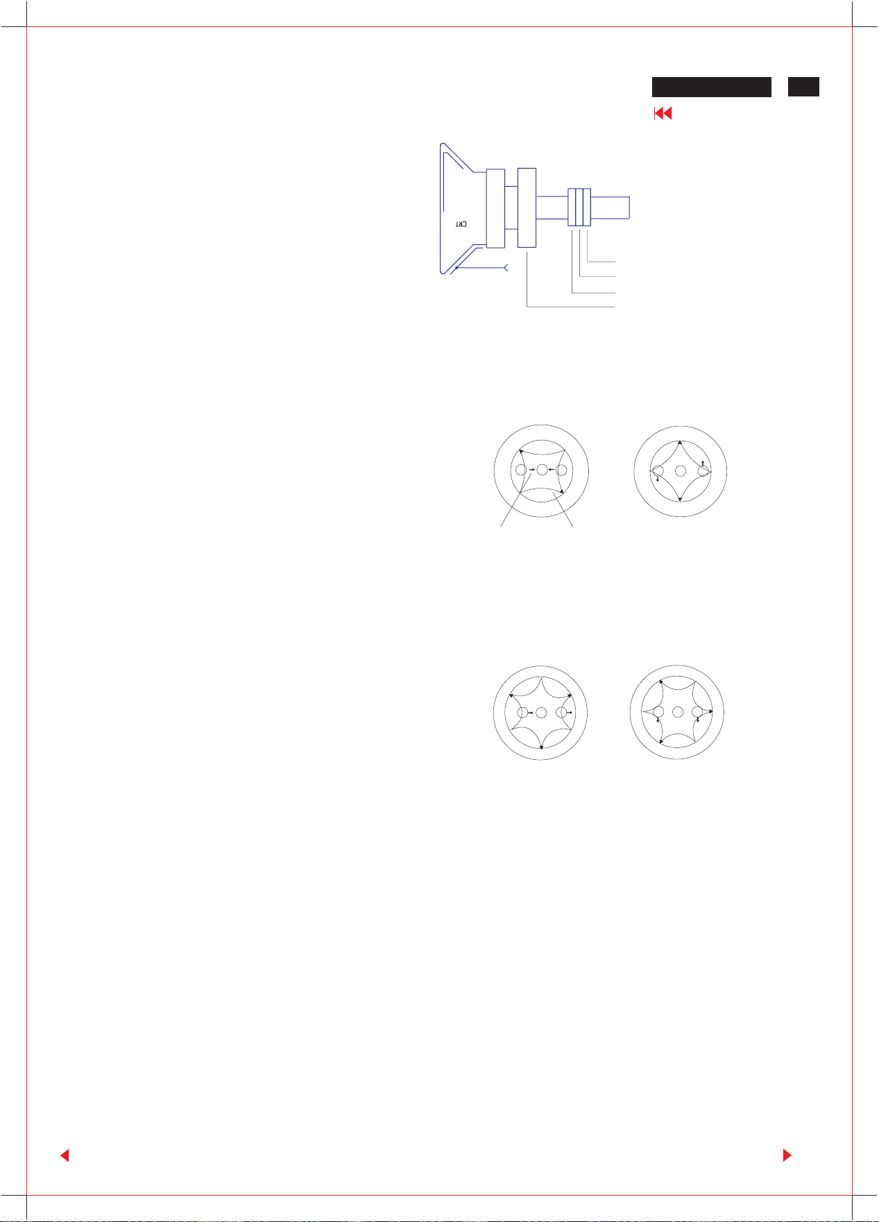
1. Purity adjustment
- Make sure the monitor is not exposed to any
external magnetic field.
- Produce a full red pattern on the screen, adjust the
purity magnet rings on the PCM assy (on CRT) to
obtain a complete field of the color red. This is done
by moving the two tabs (2-pole) in such a manner
that they advance in an opposite direction but at
the same time to obtain the same angle between
the two tabs, which should be approximately 180
degree.
- Check by full green pattern and full blue pattern
again to observe their respective color purity.
2. Static convergence
201P GS3 CM25
Go to cover page
2-pole purity magnet
6-pole convergence magnet
4-pole convergence magnet
Deflection Yoke
27
Introduction
Slight deviation in the static convergence can be
corrected by using two permanent pairs of magnets
which are fitted around the neck of the CRT. These
are the 4-pole magnet and the 6-pole magnet.
The 4-pole magnet move the outermost electron
beams (R and B) parallel in the opposite direction
from the other. The 6-pole magnet moves the
outermost electron beam (R, B and G) parallel in the
opposite direction from the other.
The magnetic field of the above magnets do not affect
the center of the CRT neck.
Setting
- Before the static convergence setting can be made,
the monitor must be switched on for 30 minutes.
- The focus setting must be made correctly.
- Signal: 640 * 480, 31.5 kHz/60 Hz mode.
- Set the tabs of the 4-pole magnet in the neutral
position. This is when the tabs are opposite one
another. In this position the magnets do not affect the
deflection of the R and B electron beams.
- Set the tabs of the 6-pole magnet in the neutral
position. This is when the tabs are opposite one
another. In this position the magnets do not affect the
deflection of the R, B, and G electron beams.
- First set the 4-pole magnet optimally.
- Then set the 6-pole magnet optimally.
- If the convergence is not now optimal, then adjust to
the optimal setting with the 4-pole magnet and then with
the 6- Pole magnet again.
- Set the tabs of the 6-pole magnet in the neutral
position. This is when the tabs are opposite one
another. In this position the magnets do not affect the
deflection of the R, B, and G electron beams.
- First set the 4-pole magnet optimally.
- Then set the 6-pole magnet optimally.
- If the convergence is not now optimal, then adjust to
the optimal setting with the 4-pole magnet and then
with the 6- pole magnet again.
4-pole Beam motion producced by the
4-pole convergence magnet
S
B
N
Beam displacement
direction
6-pole
N
G
R
S
N
B
Magnetic flux
lines
Beam motion producced by the
6- pole convergence magnet
N
S
B
N
S
R
G
N
S
S
B
N
G
S
S
G R
S
N
R
N
N
S
Back
Forward
Page 29
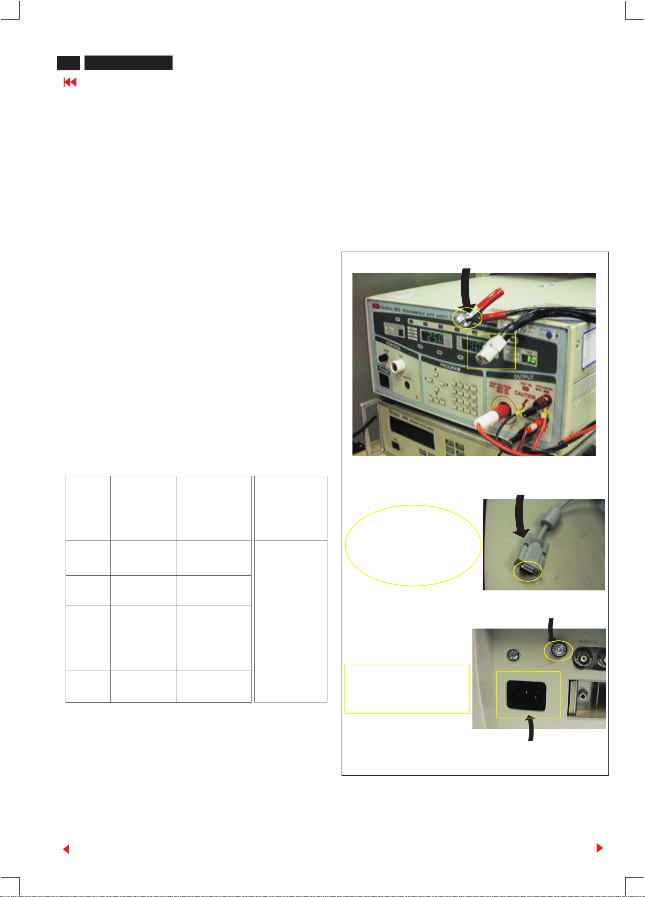
201P GS3 CM25+
28
Go to cover page
Safety test requirements
All units that are returned for service or repair must pass the
original manufactures safety tests. Safety testing requires both
and testing.Hipot Ground Continuity
HI-POT TEST INSTRUCTION
1. Application requirements
1.1 All mains operated products must pass the Hi-Pot test as
described in this instruction.
1.2 This test must be performed again after the covers have
been refitted following the repair, inspection or modification
of the product.
Test method
2.
2.1 Connecting conditions
2.1.1 The test specified must be applied between the parallel-
blade plug of the mainscord and all accessible metal
parts of the product.
2.1.2 Before carrying out the test, reliable conductive
connections must be ensured and thereafter be
maintained throughout the test period.
3. Equipments and Connection
3.1. Equipments
For example :
- ChenHwa 9032 PROGRAMMABLE AUTO SAFETY
TESTER
- ChenHwa 510B Digital Grounding Continuity Tester
- ChenHwa 901 (AC Hi-pot test), 902 (AC, DC Hi-pot test)
Withstanding Tester
3.2. Connection
* Turn on the power switch of monitor before Hipot and
Ground Continuity testing.
Clip
Clip
2.1.3 The mains switch(es) must be in the "ON" position.
2.2 Test Requirements
All products should be HiPot and Ground Continuity tested as
follows:
Condition HiPot Test for HiPot Test for Ground Continuity
products where products where Test requirement
the mains input the mains input is
range is Full 110V AC(USA
range(or 220V type)
AC)
Test 2820VDC 1700VDC Test current:
voltage (2000VAC) (1200VAC) 25A,AC
Test time:
Test time 3 seconds 1 second 3 seconds(min.)
(min.) Resistance
required:
Trip set at 100 uA 5 mA <=0.09+R ohm,
current for Max. R is the
(Tester) limitation; set resistance of
at 0.1 uA for the mains cord.
Min. limitation
Ramp set at 2
time seconds
(ChenHwa 9032 tester)
Video cable
Connect the "video cable"
or "grounding screw"
to the CLIP on your tester.
Grounding screw
Connect the power cord
to the monitor.
2.2.1 The test with AC voltage is only for production purpose,
Service center shall use DC voltage.
2.2.2 The minimum test duration for Quality Control Inspector
must be 1 minute. No breakdown during the test.
2.2.3 The test voltage must be maintained within the specified
voltage + 5%.
2.2.4 The grounding blade or pin of mains plug must be
conducted with accessible metal parts.
Back
Power outlet
4. Recording
Hipot and Ground Continuity testing records have to be kept for
a period of 10 years.
(Rear view of monitor)
Forward
Page 30
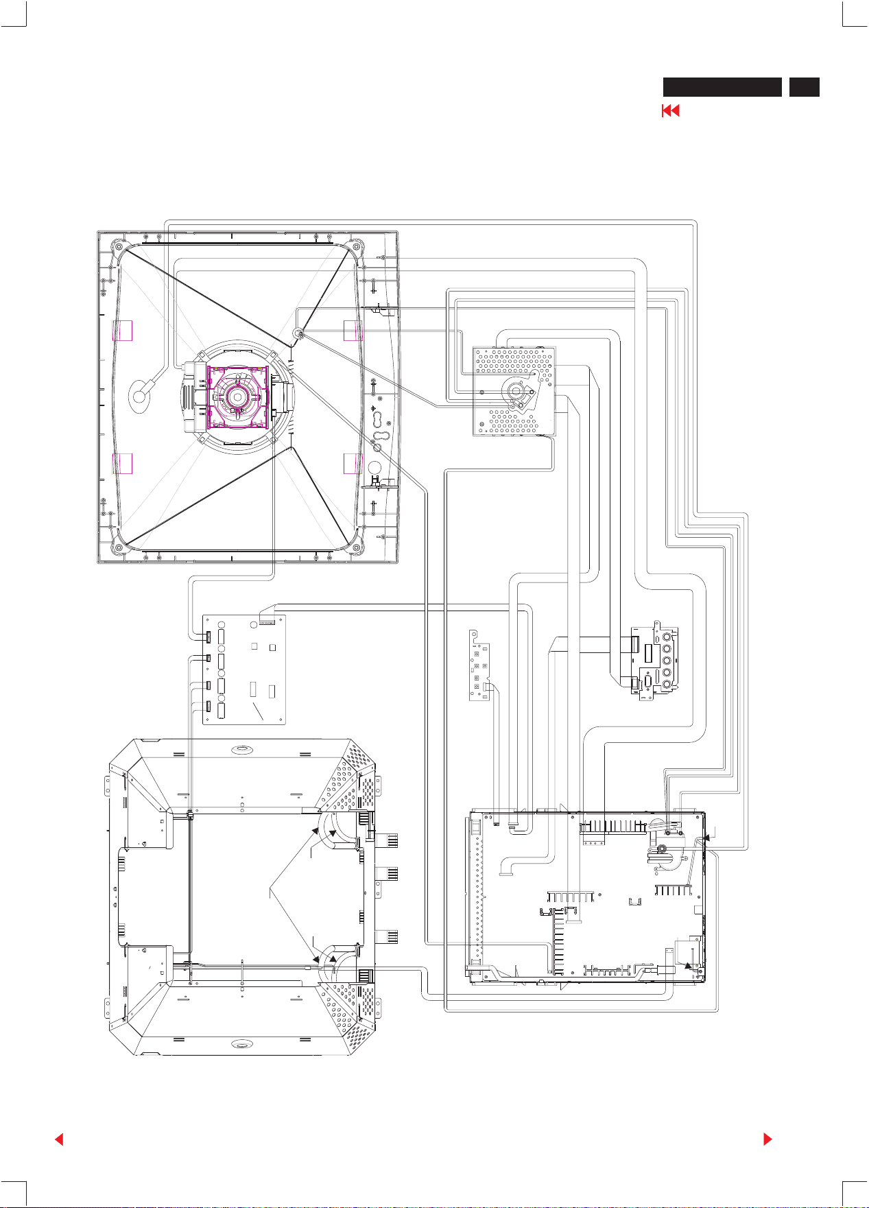
Wiring Diagram
GRAYWIRE
WHITEWIRE
201P GS3 CM25
29
Go to cover page
(For reference only)
8701
6
1
1
1706
3138 103 52910
GROUNDING WIRE
11
1
1705
10
VIDEO SHIELD
SNAP INTO
REDWIRE
9
1
6
1206
1
3
NSCOIL
1205
1
4
CORNERCOIL
RIGHTSIDE
1204
1
5
1203
1
LEFTSIDE
CORNERCOIL
1201
3138 103 52410
LEFT SIDE
CORNER COIL
RIGHT SIDE
DEGAUSSING COIL
CORNER COIL
1
8891
7
3138 103 52290
8002
12
1
7
1
1311
1
9
1310
11
1
8001
4
11
1
8003
3138 103 52400
1502
1
2
10
1006
1
3138 103 51940
6
1003
1
BOTTOMSHIELD
GROUNDING WIRE
SNAP INTO
1
1501
GROUNDING WIRE
FIXED WITH SCREW
1311
3
1
Back
Forward
Page 31
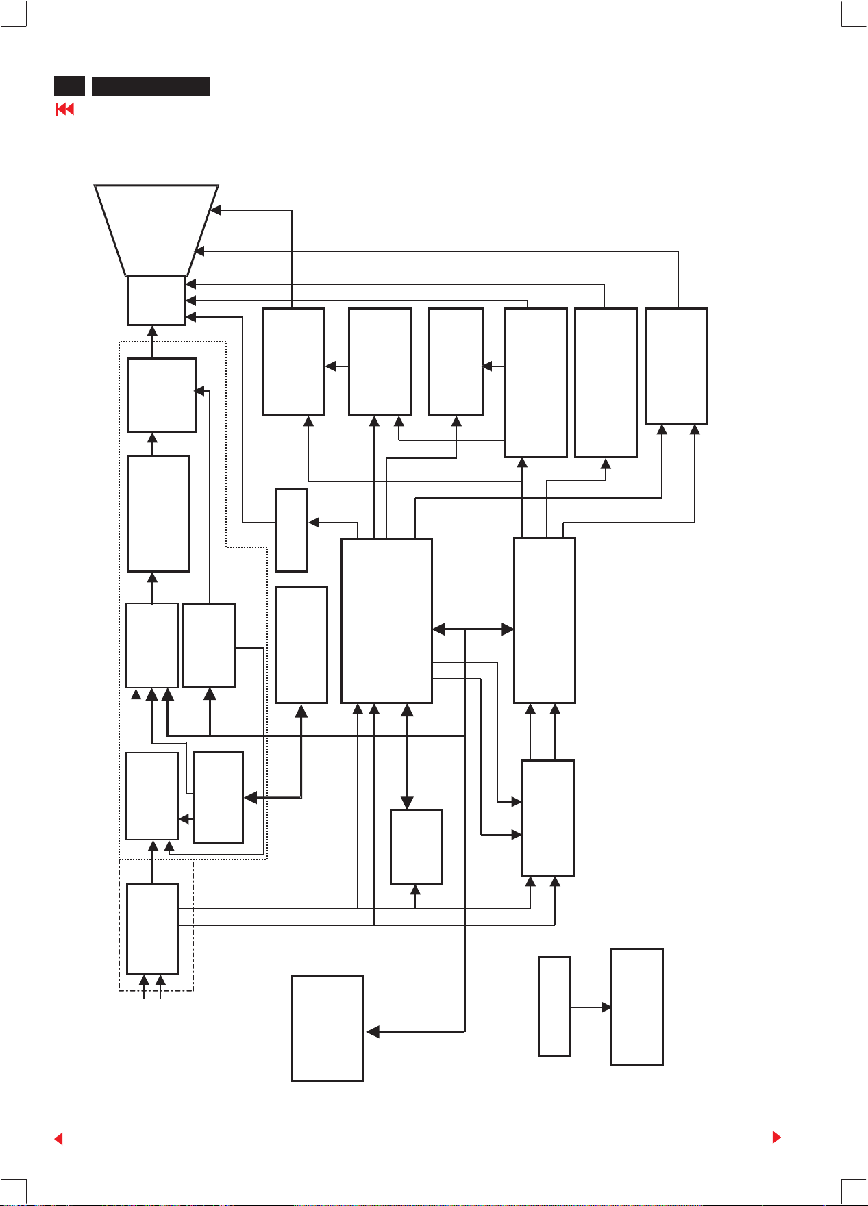
30
201P GS3 CM25
Go to cover page
CRT
DC
Restore
(discrete)
EHT
Block Diagram
DAF
X-RAY
Cs SW
Linearity
Control
Horizontal
Deflection
.
Vertical
STV9379
Muting & G1
G1
Spot Killer
MUTE
HUNLOCK
” MONITOR
CM25+ 201P 21
Post-Amp
CR 6927
Amp
-
M52742SP
Pre
R/G/B BUFFER
& OSD SIGNAL
SELECTOR
B
R
G
Signal
Selector
Auto
Calibrate
.
OSD
LSC4588P2
HV
Rotation
D11
USB device
.
SDA
SCL
.
CPU
.
P83C380
SDA/SCL
(DDC)
DDC
1/2B
.
.
.
B+
’
V
H’
HDRV
Sync Processor
H”
Sync
TDA4856
”
V
Switch
+210
Horizontal Frequency : 30~121kHz
+81
+15
-15
Vertical Frequency : 50~160 Hz
+6.3
Back
BNC
D-SUB
Purity &
correction
convergence
Degaussing
Power
Supply
Forward
Page 32
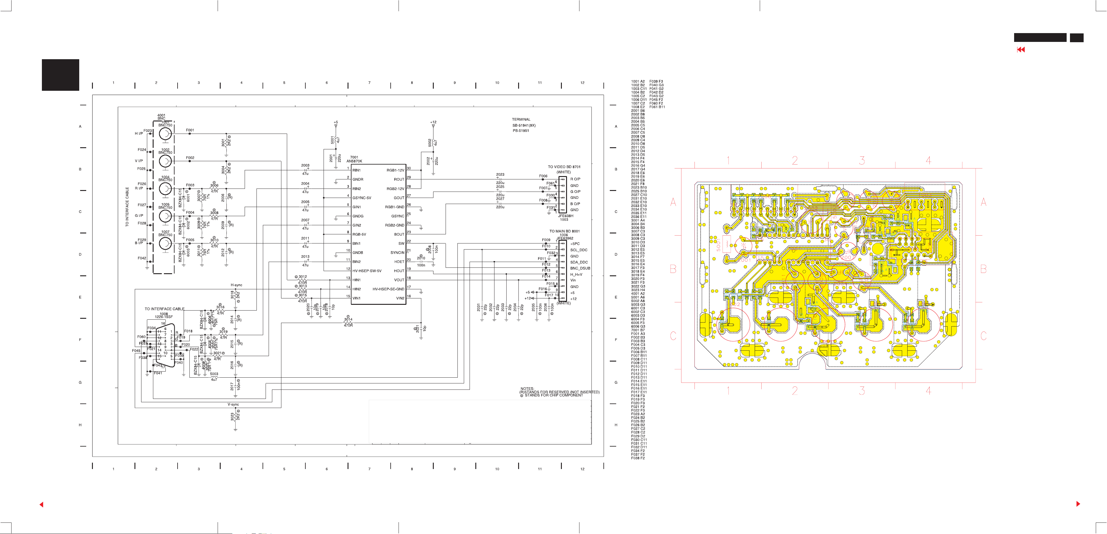
A1
Terminal Schematic Diagram
PCB (A1)
201P GS3 CM25
Go to cover page
# GRID BOARD
# REF LABEL SIDE
# ____ _____ _________
1001 C2 B 2036 A1 A
1002 C1 B 3001 C2 A
1003 A4 B 3004 C1 A
1004 C4 B 3006 C4 A
1005 C3 B 3007 C4 A
1006 A2 B 3008 C3 A
1007 C2 B 3009 C3 A
1008 B4 B 3010 C2 A
2001 B1 B 3011 C2 A
2002 A2 B 3012 B1 A
2003 B3 B 3013 B1 A
2004 B3 B 3014 A1 A
2005 B2 B 3015 B1 A
2007 B3 B 3016 B3 A
2011 B2 B 3017 B3 A
2013 A3 B 3018 B4 A
2023 A4 B 3019 A3 A
2025 A3 B 3020 A3 A
2027 A3 B 3021 A3 A
4001 C3 B 3022 A4 A
5001 B1 B 3023 B4 A
5002 A3 B 6001 C4 A
5003 A3 B 6002 C3 A
7001 B2 B 6003 C2 A
2006 C4 A 6004 B3 A
2008 A2 A 6005 A3 A
2009 C3 A
2010 A2 A
2012 C2 A
2014 B3 A
2015 A3 A
2016 A3 A
2017 A3 A
2018 B1 A
2019 B1 A
2020 B1 A
2021 A2 A
2031 A2 A
2032 A2 A
2033 A1 A
2034 A1 A
2035 A1 A
6006 A4
32
31
Back
P
Forward
Page 33
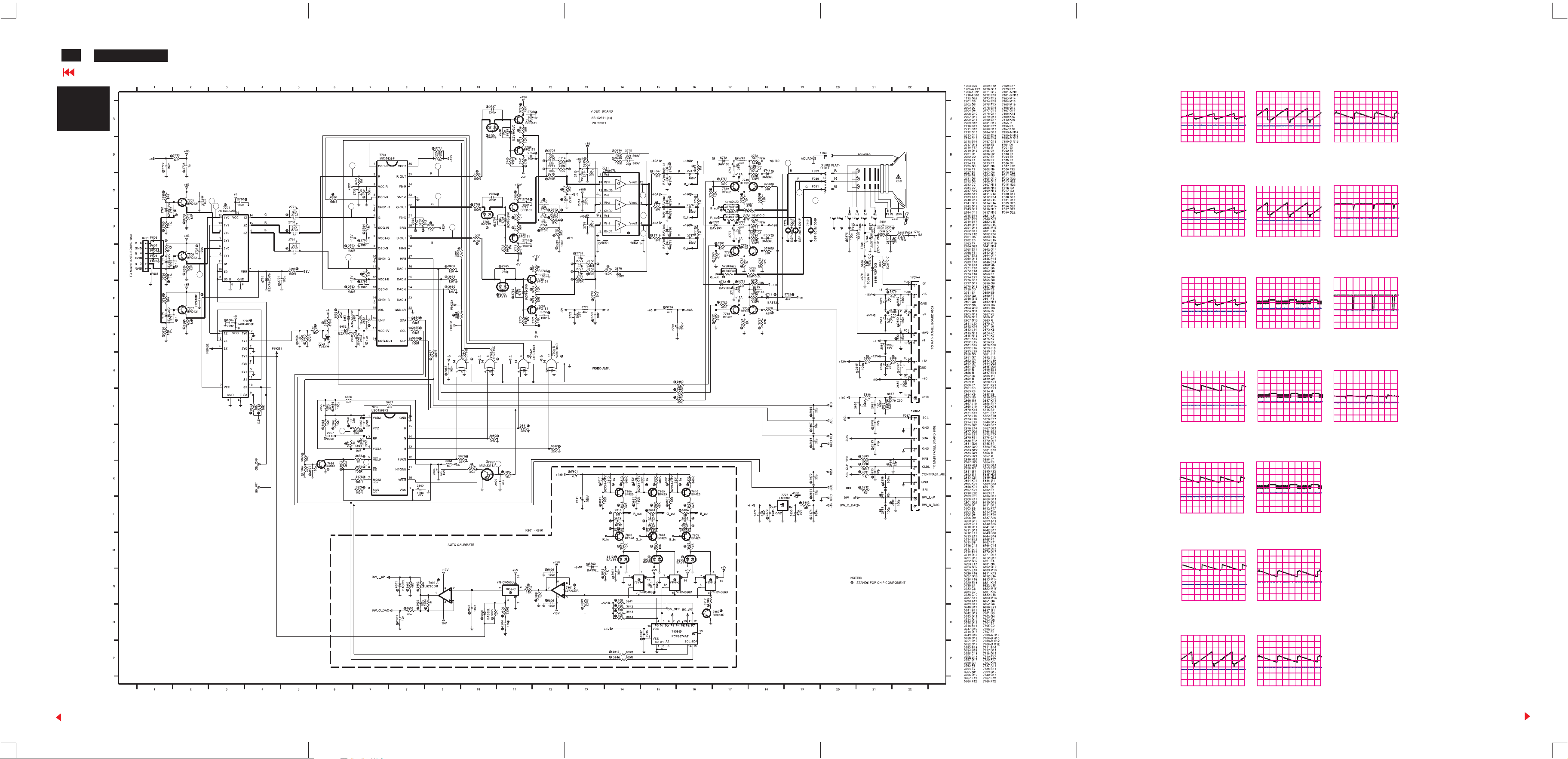
32
32
201P GS3 CM25
Go to cover page
A2
Video Schematic Diagram
Waveform (A)
A1 7701-2 A3 7704-32 A5 1710-7
2.1V
1.3V
52.6V
A2
2.6V
A1
A1
1.3V
1.3V
1.3V
A1
2.6V
2.6V
A2
A2
5.7V
6.2V
4.3V
4.7V
2.8V
A3
3V
A3
2.9V
A3
1.3V
1.3V
1.3V
52.9V
A4
A4
A4
53.9V
A5
75.7V
74.4V
A5
A5
76.5V
1 V/div AC
10 uS/div
20 V/div AC
10 uS/div
A1 7701-5 A3 7704-29 A6 7855-2
1 V/div AC
10 uS/div
20 V/div AC
10 uS/div
A1 7701-12 A4 7711-12 A7 7855-5
1 V/div AC
10 uS/div
50 V/div AC
5 mS/div
A2 7704-2 A4 7711-8 A8 7857-B
50 V/div AC
10 uS/div
0.5 V/div AC
10 uS/div
2 V/div AC
10 uS/div
A6
1.1V
4.6V
A7
5V
5V
5V
5V
5V
A8
75.8V
1 V/div AC
10 uS/div
A2 7704-6
1 V/div AC
10 uS/div
50 V/div AC
5 mS/div
A4 7711-4
50 V/div AC
5 mS/div
0.5 V/div AC
10 uS/div
A2 7704-11 A5 1710-12
1 V/div AC
10 uS/div
50 V/div AC
10 uS/div
A3 7704-35 A5 1710-9
Back
20 V/div AC
10 uS/div
50 V/div AC
10 uS/div
Forward
Page 34
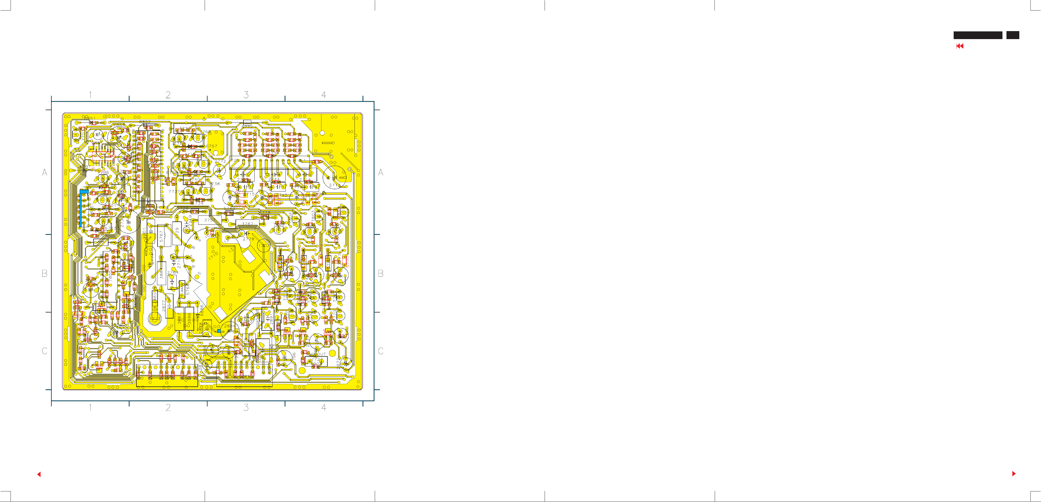
PCB (A2,Video)
1703 B3 B 3753 B4 B 7767 A2 B 2703 A2 2892 C2 3774 A4 3870 B1 7857 B1
1705 C3 B 3754 B4 B 7768 A2 B 2704 A2 2893 C2 3775 A4 3871 B2
1706 C2 B 3757 A3 B 7769 B4 B 2707 A2 2894 C2 3776 A4 3872 B2
1710 B3 B 3770 A2 B 7770 C4 B 2709 A3 2895 C2 3777 A4 3873 B1
1712 C2 B 3783 B4 B 7803 A4 B 2710 A3 2896 C2 3778 A3 3874 B2
2701 A1 B 3784 B4 B 7804 A4 B 2711 A3 2897 C2 3780 B4 3875 C1
2713 A4 B 3787 A3 B 7805 A4 B 2712 A3 2898 C2 3781 B4 3876 C1
2714 A4 B 3884 B2 B 7808 A4 B 2721 A1 2899 C2 3782 C4 3878 B1
2715 A3 B 3885 B2 B 7809 A3 B 2722 A1 2900 C1 3785 B4 3879 B1
2717 A3 B 3886 C2 B 7810 A4 B 2723 A1 3700 A1 3786 B4 3880 B1
2718 B4 B 3887 C2 B 7855 B1 B 2724 A1 3703 A1 3795 A1 3881 B1
2719 B2 B 3888 C3 B 8701 A1 B 2725 B1 3704 A2 3797 A1 3882 B1
2731 A1 B 4902 C4 B 2726 A1 3705 A2 3799 A1 3883 C4
2733 A1 B 5715 A2 B 2727 A1 3706 A2 3801 B1 3889 C2
2744 A3 B 5728 A2 B 2728 A1 3708 A2 3802 B1 3890 C2
2745 A3 B 5748 A3 B 2732 A1 3709 A2 3803 C1 3891 C2
2747 A3 B 5767 B2 B 2734 A2 3710 A2 3804 C1 3892 C2
2748 B4 B 5768 B2 B 2738 A2 3711 A2 3805 C1 3896 A3
2749 A2 B 5772 A3 B 2740 A3 3714 A3 3806 C1 3897 C1
2761 A2 B 5778 A3 B 2741 A3 3716 A3 3808 C1 3898 A2
2764 B2 B 5856 B2 B 2742 A3 3717 A3 3809 C1 5721 B4
2768 A3 B 5857 B1 B 2743 A3 3718 A3 3811 A4 5722 B3
2772 A3 B 5858 B2 B 2762 A1 3719 A3 3812 B4 5749 B4
2774 B2 B 5864 C1 B 2763 A2 3722 B4 3815 C4 5779 B4
2776 A4 B 5875 C3 B 2766 A2 3723 B3 3816 C4 5795 A1
2777 B4 B 5888 C3 B 2769 A4 3724 C4 3817 C1 5796 C3
2778 B3 B 6701 A1 B 2770 A4 3727 B3 3823 A3 5801 C4
2796 C4 B 6702 A1 B 2771 A4 3728 B3 3825 C3 5879 C3
2811 C4 B 6703 A1 B 2773 A4 3730 A1 3832 B4 5880 C3
2833 C4 B 6708 A2 B 2801 C1 3734 A2 3833 A4 5885 C3
2851 A1 B 6739 A2 B 2802 C1 3737 A2 3834 A4 5886 C3
2853 A1 B 6767 A3 B 2804 C1 3738 A2 3835 C4 5889 A4
2855 B1 B 6791 A1 B 2805 C1 3739 A2 3841 C1 6710 A3
2863 B1 B 6851 A1 B 2807 C1 3742 A3 3842 C1 6711 A3
2864 C1 B 6852 A2 B 2814 C4 3743 A3 3843 C1 6713 B3
2872 C4 B 6886 B2 B 2832 A4 3744 A3 3844 C1 6740 A3
2876 A4 B 6887 C3 B 2852 A2 3745 A3 3852 A1 6741 A3
2877 B2 B 7703 A1 B 2854 A2 3746 A3 3853 A1 6742 B4
2878 C2 B 7704 A2 B 2856 B1 3747 A3 3854 A2 6743 B4
2879 C2 B 7705 A1 B 2858 B1 3748 A3 3855 A2 6768 A4
2881 C3 B 7706 A1 B 2859 B1 3750 B4 3856 A2 6769 A4
2884 C3 B 7707 A1 B 2860 B2 3751 B4 3857 A2 6770 B4
2886 C2 B 7711 A3 B 2861 B1 3752 C4 3858 A2 6771 B4
2889 C3 B 7717 A2 B 2865 B1 3755 B4 3859 A2 6801 C1
2890 C3 B 7718 A3 B 2873 C4 3756 B4 3860 A2 6803 C3
2891 C3 A 7719 B4 B 2874 C4 3760 A1 3862 A2 6813 C4
2901 A2 B 7720 C4 B 2875 A3 3764 A2 3863 A2 6823 C4
3712 A2 B 7727 C4 B 2880 C3 3767 A2 3864 A2 6832 A4
3725 B3 B 7737 A2 B 2882 C3 3768 A2 3866 C1 6833 C4
3726 B3 B 7738 A3 B 2883 C3 3769 A2 3867 B1 7701 A1
3729 A2 B 7739 B4 B 2885 C3 3772 A4 3868 B1 7807 C1
3740 A2 B 7740 C4 B 2887 C3 3773 A4 3869 B1 7856 B1
Back
201P GS3 CM
Go to cover page
Forward
25
33
Page 35
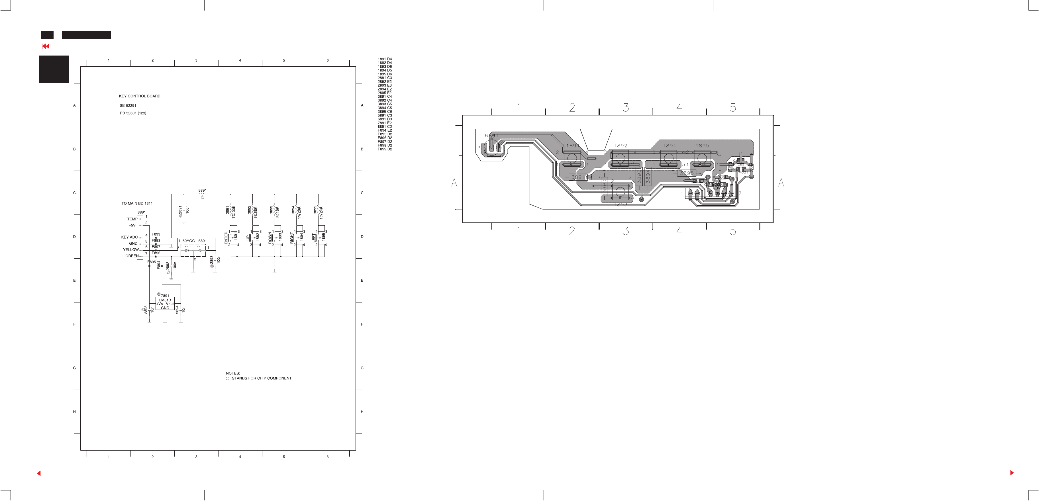
32
34
201P GS3 CM25
Go to cover page
E
Key Control Schematic Diagram
Control Panel P.C.B.(E)
# GRID BOARD
# REF LABEL SIDE
# ____ _____ _________
1891 A2 B
1892 A3 B
1893 A3 B
1894 A4 B
1895 A4 B
3891 A2 B
3892 A3 B
3893 A3 B
3894 A3 B
3895 A4 B
6891 A1 B
8891 A5 B
2891 A5 A
2892 A5 A
2893 A5 A
2894 A5 A
2895 A5 A
5891 A4 A
7891 A5 A
BackBack
Forward
Page 36
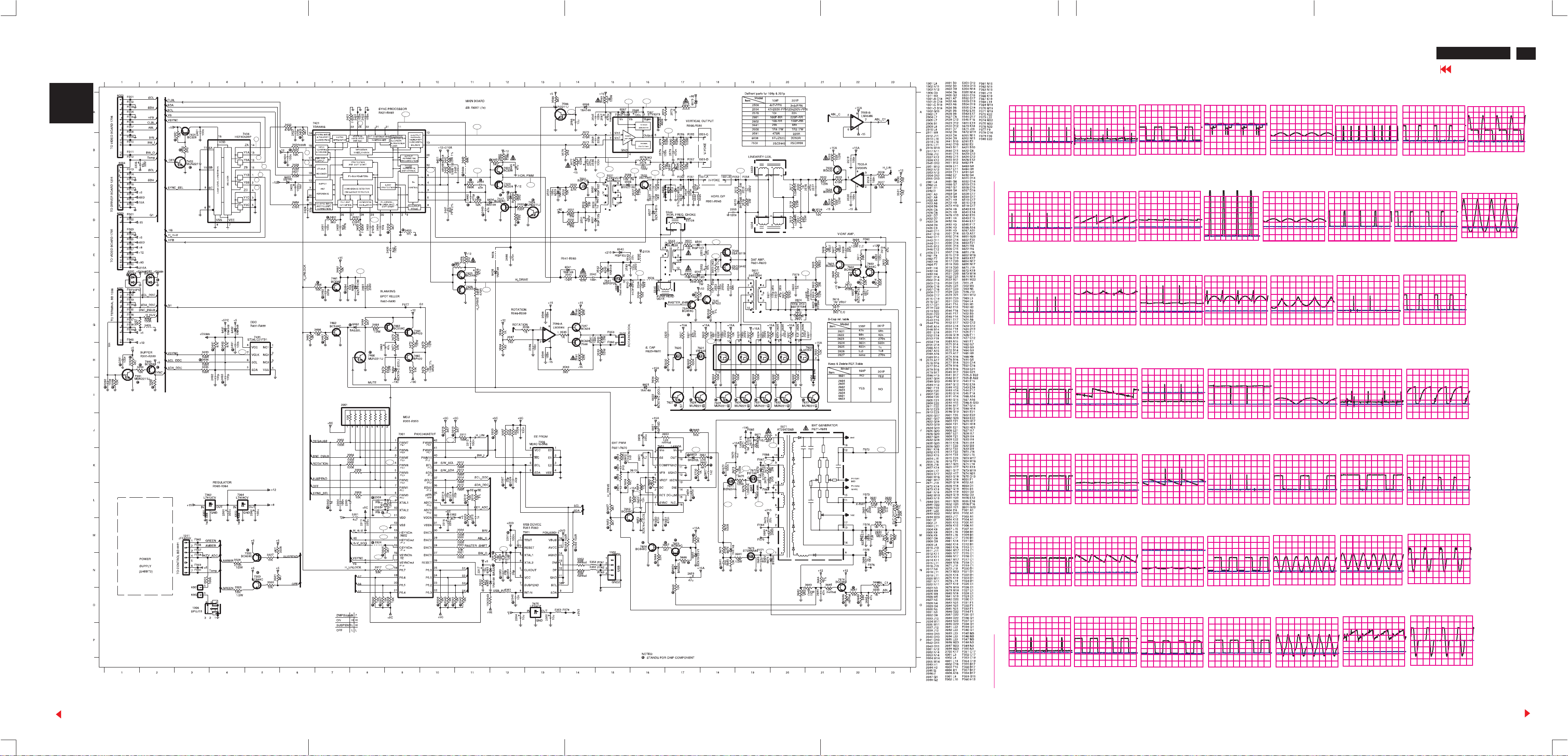
Deflection Schematic Diagram
201P GS3 CM25
Go to cover page
32
35
B
B1 7404-14
B18
B17
B10
B9
B1
B2
B3
B4
B5
B6
B26
B7
B8
B12
B13
B25
B11
B14
B15
B27
B16
B19
B20
B22
B21
B23
B28
B32
B24
B29
B30
B31
B1 7404-14
2 V/div AC
5 mS/div
2 V/div AC
5 mS/div
B2 7404-13
B2 7404-13
2 V/div AC
2 V/div AC
5 mS/div
5 mS/div
B3 7404-12
B3 7404-12
2 V/div AC
2 V/div AC
5 mS/div
5 mS/div
B4 7404-15
B4 7404-15
B8 7421-17
B8 7421-17
0.5 V/div AC
5 mS/div
0.5 V/div AC
5 mS/div
B9 7421-24
B9 7421-24
2 V/div AC
2 V/div AC
5 mS/div
5 mS/div
B10 7421-11 B17 7567-6
B10 7421-11 B17 7567-6
1 V/div AC
1 V/div AC
5 mS/div
5 mS/div
B11 7421-12 B18 7567-3
B11 7421-12 B18 7567-3
B15 7422-E
B15 7422-E
5 V/div AC
5 uS/div
5 V/div AC
5 uS/div
B16 7566-B
B16 7566-B
10 V/div AC
10 V/div AC
5 mS/div
5 mS/div
10 V/div AC
10 V/div AC
5 mS/div
5 mS/div
B22 7502-B
B22 7502-B
5 V/div AC
5 uS/div
5 V/div AC
5 uS/div
B23 7502-C
B23 7502-C
100 V/div AC
100 V/div AC
5 uS/div
5 uS/div
B24 5503-5
B24 5503-5
50 V/div AC
50 V/div AC
5 uS/div
5 uS/div
B25 7461-C
B25 7461-C
B29 7543-C
B29 7543-C
B36 7301-13
B36 7301-13
100 V/div AC
5 uS/div
100 V/div AC
5 uS/div
2 V/div AC
10 uS/div
B30 7543-B B37 7301-14
B30 7543-B B37 7301-14
100 V/div AC
100 V/div AC
5 uS/div
5 uS/div
B31 5601-4
B31 5601-4
100 V/div AC
100 V/div AC
5 mS/div
5 mS/div
B32 7622-11
B32 7622-11
2 V/div AC
2 V/div AC
5 uS/div
5 uS/div
B38 7301-16
B38 7301-16
2 V/div AC
2 V/div AC
5 mS/div
5 mS/div
B39 7301-18
B39 7301-18
B43 7651-1
B43 7651-1
2 V/div AC
10 uS/div
2 V/div AC
5 uS/div
2 V/div AC
5 uS/div
B44 7651-10
B44 7651-10
5 V/div AC
5 V/div AC
5 uS/div
5 uS/div
B45 7671-G
B45 7671-G
5 V/div AC
5 V/div AC
5 uS/div
5 uS/div
B46 7671-D
B46 7671-D
B50 5671-1
B50 5671-1
100 V/div AC
5 uS/div
100 V/div AC
5 uS/div
B51 5671-12
B51 5671-12
100 V/div AC
100 V/div AC
5 uS/div
5 uS/div
Back
0.2 V/div AC
0.2 V/div AC
10 uS/div
B40
B44
B33
B34
B35
B36
B37
B41
B38
B39
B42
B43
B46
B45
B48
B49
B47
B50
B51
10 uS/div
B5 7404-1
B5 7404-1
0.2 V/div AC
10 uS/div
0.2 V/div AC
10 uS/div
B6 7404-2
B6 7404-2
0.2 V/div AC
10 uS/div
0.2 V/div AC
B7 7421-16
10 uS/div
B7 7421-16
2 V/div AC
5
5 uS/div
2 V/div AC
5
5 uS/div
0.5 V/div AC
0.5 V/div AC
2 mS/div
2 mS/div
B12 7421-32
B12 7421-32
5 V/div AC
5 mS/div
5 V/div AC
5 mS/div
B13 7421-29
B13 7421-29
2 V/div AC
5 uS/div
2 V/div AC
B14 7422-B
5 uS/div
B14 7422-B
5 V/div AC
5 US/div
5 V/div AC
5 US/div
10 V/div AC
10 V/div AC
5 mS/div
5 mS/div
B19 7567-5
B19 7567-5
20 V/div AC
5 mS/div
20 V/div AC
5 mS/div
B20 7567-4
B20 7567-4
5 V/div AC
5 mS/div
5 V/div AC
B21 5501-5
5 mS/div
B21 5501-5
50 V/div AC
5 uS/div
50 V/div AC
5 uS/div
5 V/div AC
5 V/div AC
5 mS/div
5 mS/div
B26 7491-7
B26 7491-7
2 V/div AC
5 mS/div
2 V/div AC
5 mS/div
B27 7425-E
B27 7425-E
5 V/div AC
5 uS/div
5 V/div AC
B28 7541-D
5 uS/div
B28 7541-D
100 V/div AC
5 uS/div
100 V/div AC
5 uS/div
20 V/div AC
20 V/div AC
5 uS/div
5 uS/div
B33 7301-4
B33 7301-4
2 V/div AC
20 uS/div
2 V/div AC
20 uS/div
B34 7301-9 B41 7351-3
0.1 V/div AC
0.1 V/div AC
5 mS/div
5 mS/div
B40 7301-42
B40 7301-42
2 V/div AC
20 uS/div
2 V/div AC
20 uS/div
B34 7301-9 B41 7351-3
2 V/div AC
50 uS/div
2 V/div AC
B35 7301-10
50 uS/div
B35 7301-10
2 V/div AC
50 uS/div
2 V/div AC
50 uS/div
1 V/div AC
50 uS/div
1 V/div AC
B42 7651-2
50 uS/div
B42 7651-2
0.5 V/div AC
5 uS/div
0.5 V/div AC
5 uS/div
5 V/div AC
5 V/div AC
5 uS/div
5 uS/div
B47 7672-D
B47 7672-D
100 V/div AC
5 uS/div
100 V/div AC
5 uS/div
B48 5671-9
B48 5671-9
100 V/div AC
5 uS/div
100 V/div AC
B49 5671-3
5 uS/div
B49 567-3
100 V/div AC
5 uS/div
100 V/div AC
5 uS/div
Forward
Page 37
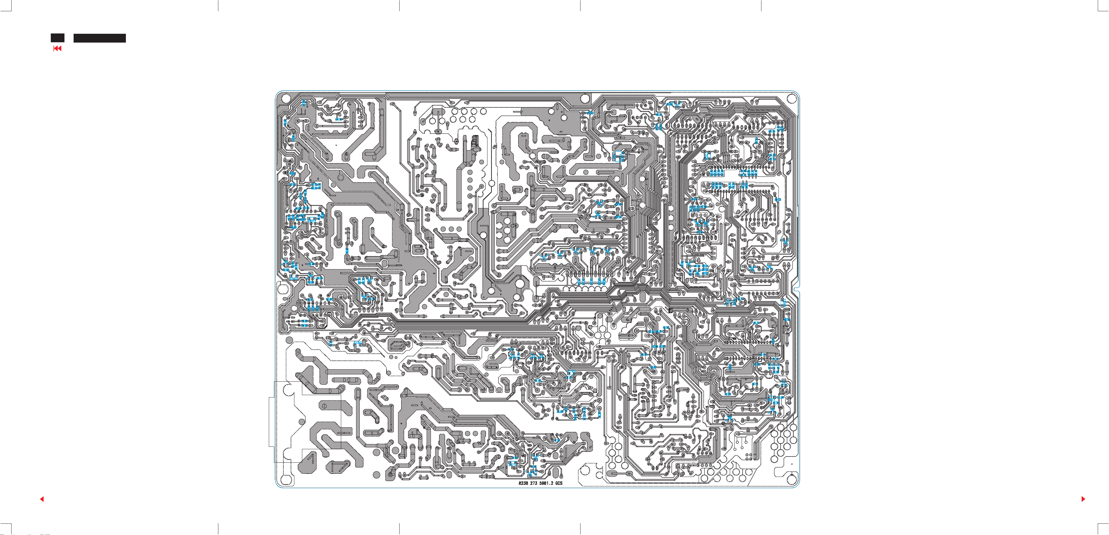
32
36-1
201P GS3 CM25
Go to cover page
Deflection/Power Panel P.C.B.(B,C)
CLICK HERE FOR COMPONENT LAYER
Back
Forward
Page 38
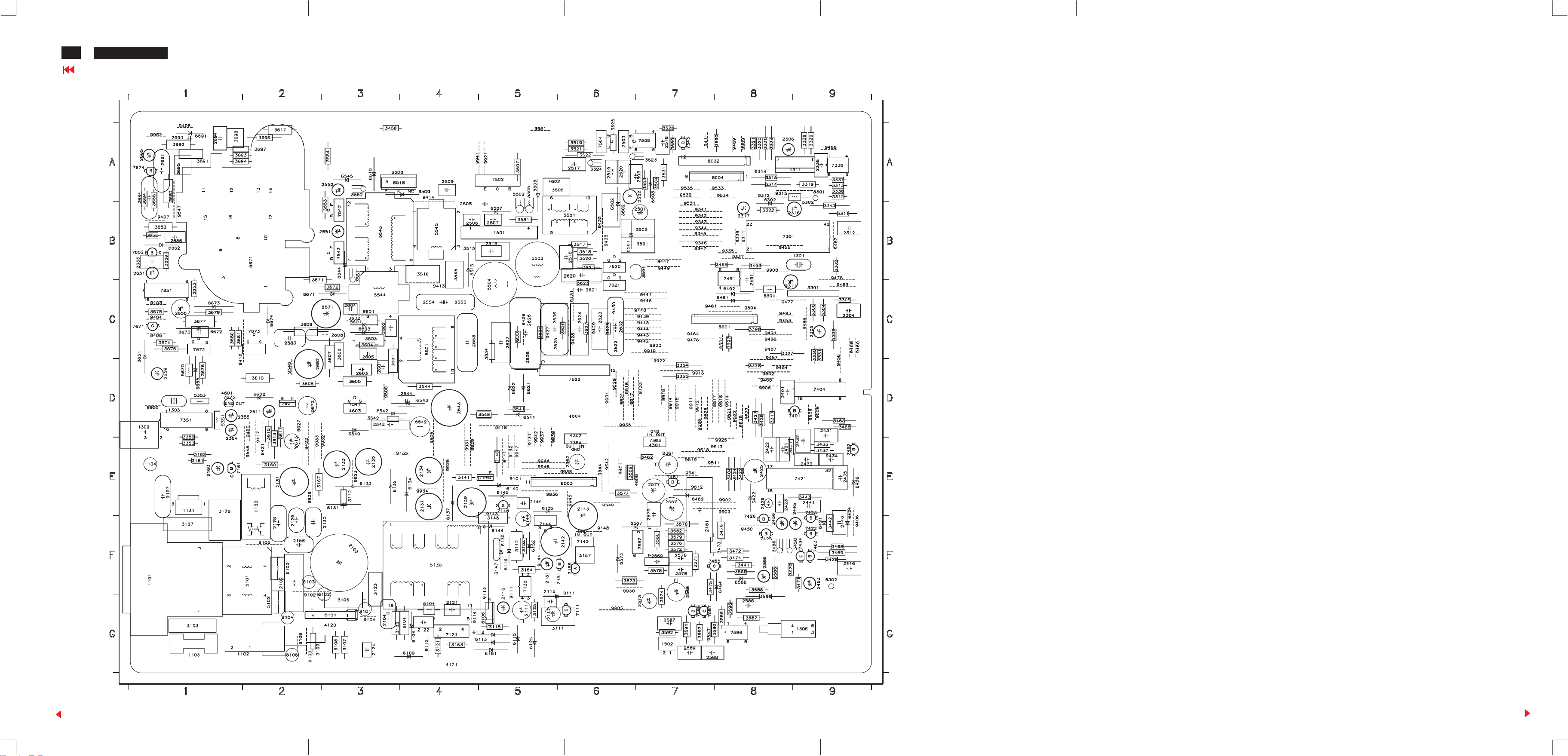
32
36
201P GS3 CM25
Go to cover page
Deflection/Power Panel P.C.B.(B,C)
1101 F1 B
1102 G2 B
1103 G1 B
1130 E2 B
1131 E1 B
1134 E1 B
1301 B9 B
1302 D1 B
1303 D1 B
1306 G9 B
1311 A9 B
1501 B5 B
1502 G7 B
2102 F2 B
2103 F3 B
2104 G3 B
2111 G5 B
2112 G5 B
2115 F5 B
2116 F5 B
2121 G4 B
2122 G4 B
2124 G3 B
2127 E1 B
2128 F2 B
2129 F2 B
2130 F3 B
2131 E2 B
2133 E3 B
2134 E4 B
2135 E3 B
2137 E4 B
2139 E4 B
2142 F6 B
2143 E6 B
2144 F5 B
2145 E5 B
2151 F5 B
2156 F2 B
2160 E1 B
2304 C9 B
2305 C9 B
2306 A8 B
2311 C8 B
2312 B9 B
2316 B9 B
2317 B8 B
2336 A9 B
2354 E1 B
2355 D2 B
2361 E7 B
2362 E6 B
2401 D8 B
2421 E8 B
2422 E8 B
2423 E8 B
2425 E8 B
2426 E8 B
2431 D9 B
2432 E9 B
2433 E9 B
2434 E9 B
2435 E9 B
2440 F9 B
2441 E9 B
2445 E9 B
2446 F9 B
2456 F8 B
2461 F7 B
2463 F9 B
2491 B8 B
2501 B7 B
2502 A7 B
2503 A7 B
2506 B4 B
2507 B5 B
2508 B4 B
2509 A4 B
2515 B5 B
2516 B6 B
2517 A6 B
2518 A7 B
2519 A6 B
2520 A6 B
2542 D3 B
2543 D4 B
2544 D4 B
2551 B3 B
2552 A3 B
2553 C4 B
2554 C4 B
2555 C4 B
2566 F8 B
2567 E7 A
2568 F7 B
2569 F7 B
2573 G7 B
2576 F7 B
2577 E7 B
2578 F7 B
2579 E7 B
2586 G8 B
2587 G7 B
2588 G7 B
2589 G7 B
2601 D3 B
2602 C3 B
2603 D3 B
2604 C3 B
2605 C3 B
2608 C3 B
2611 D2 B
2613 E2 B
2620 B6 B
2621 C6 B
2622 C6 B
2623 C6 B
2624 C6 B
2625 C5 B
2626 C5 B
2627 C5 B
2632 C6 B
2635 C5 B
2636 C5 B
2651 B1 B
2655 B1 B
2656 C1 B
2659 D1 B
2671 C3 B
2673 C1 B
2682 D2 B
2683 C2 B
2684 A1 B
2685 A1 B
2686 B1 B
2691 A1 B
2693 A1 B
2694 A1 B
3103 G1 B
3104 G4 B
3105 G3 B
3106 G3 B
3107 G3 B
3108 G3 B
3109 G2 B
3111 G6 B
3112 E3 B
3115 G5 B
3121 G4 B
3123 F3 B
3125 G5 B
3127 F1 B
3128 E1 B
3141 E4 B
3142 F5 B
3145 F5 B
3146 E5 B
3147 F5 B
3152 F5 B
3154 F5 B
3157 F6 B
3160 E2 B
3161 E1 B
3162 E1 B
3163 G4 B
3167 E2 B
3301 C9 B
3302 B9 B
3304 C9 B
3305 C9 B
3306 C9 B
3309 C9 B
3311 B9 B
3312 A9 B
3313 A9 B
3314 A8 B
3315 A8 B
3317 D8 B
3319 A9 B
3320 A8 B
3321 A8 B
3322 B8 B
3326 D8 B
3327 C8 B
3328 A9 B
3329 A9 B
3330 C9 B
3331 C9 B
3334 A8 B
3335 A8 B
3337 A9 B
3338 A9 B
3343 B9 B
3352 D1 B
3353 E1 B
3354 D7 B
3355 D7 B
3397 C8 B
3398 C8 B
3404 E8 B
3421 E8 B
3422 E8 B
3424 E8 B
3426 D8 B
3427 D8 B
3428 F9 B
3432 E9 B
3433 E9 B
3441 F8 B
3442 F9 B
3443 E9 B
3450 F9 B
3456 F8 B
3458 A3 B
3462 E7 B
3465 D9 B
3466 D9 B
3468 F9 B
3469 F9 B
3470 F8 B
3471 F9 B
3472 F8 B
3473 F8 B
3474 F8 B
3475 F7 B
3476 F8 B
3493 B8 B
3495 B8 B
3501 B7 B
3502 B6 B
3503 A7 B
3504 A7 B
3505 B7 B
3506 A6 B
3507 A5 B
3515 B4 B
3516 B4 B
3517 B6 B
3518 B6 B
3519 A6 B
3520 B6 B
3521 A6 B
3522 A6 B
3523 A7 B
3524 A6 B
3525 A6 B
3528 A7 B
3531 A7 B
3541 D5 B
3542 D3 B
3544 D4 B
3545 B4 B
3546 D5 B
3551 B3 B
3552 A3 B
3553 B3 B
3554 A3 B
3566 F8 B
3569 E6 B
3570 F7 B
3571 F7 B
3572 F7 B
3573 F6 B
3574 G7 B
3576 F7 B
3577 E6 B
3578 F7 B
3579 F7 B
3580 F7 B
3581 B5 B
3582 F7 B
3586 F8 B
3587 G8 B
3588 F8 B
3589 G8 B
3590 G8 B
3591 G7 B
3592 G7 B
3593 G7 B
3594 B7 B
3595 G8 B
3596 G8 B
3601 D3 B
3602 C3 B
3603 C3 B
3604 C3 B
3605 D3 B
3606 C3 B
3607 C3 B
3608 D2 B
3609 C2 B
3611 D2 B
3613 E2 B
3615 D2 B
3616 D2 B
3617 A2 B
3621 B6 B
3623 C6 B
3625 C6 B
3627 C6 B
3629 C6 B
3631 C5 B
3633 C5 B
3634 C5 B
3653 C1 B
3658 B1 B
3659 B1 B
3671 B2 B
3672 C3 B
3674 C1 B
3675 C1 B
3676 D1 B
3677 C1 B
3678 C1 B
3679 C1 B
3680 C1 B
3681 C1 B
3682 A1 B
3683 B1 B
3684 A1 B
3685 A1 B
3689 A7 B
3690 A8 B
3691 A1 B
3692 A1 B
3693 A1 B
3694 A1 B
3695 A1 B
3696 A2 B
3697 A2 B
3698 A1 B
4120 G3 B
4121 G4 B
4301 E7 B
4302 D6 B
4601 D1 B
4602 A5 B
4603 D3 B
4604 D6 B
4606 E7 B
5101 F2 B
5102 G2 B
5103 F2 B
5104 G4 B
5130 F4 B
5301 C8 B
5302 B9 B
5351 D1 B
5353 D1 B
5501 B6 B
5502 A5 B
5503 B5 B
5504 C5 B
5505 A5 B
5542 D4 B
5543 B3 B
5544 C3 B
5545 B4 B
5601 C4 B
5670 D1 B
5671 B2 B
5672 D2 B
6101 G3 B
6104 G4 B
6109 G4 B
6111 F6 B
6112 G5 B
6113 G5 B
6115 G5 B
6116 F5 B
6125 G5 B
6131 E3 B
6132 E5 B
6133 E3 B
6134 E4 B
6135 E3 B
6137 E4 B
6139 F5 B
6140 E5 B
6144 F5 B
6145 E5 B
6152 F5 B
6161 G5 B
6302 A8 B
6421 F9 B
6422 E8 B
6424 E9 B
6426 E9 B
6462 E7 B
6464 F8 B
6491 C8 B
6492 C8 B
6501 B6 B
6502 B6 B
6503 A7 B
6506 A5 B
6507 B5 B
6508 A3 B
6509 A4 B
6510 A3 B
6515 B4 B
6518 A3 B
6540 D3 B
6541 D5 B
6542 D3 B
6543 D4 B
6544 B3 B
6545 A3 B
6566 F8 B
6567 F7 B
6573 F6 B
6601 C3 B
6602 D2 B
6603 C3 B
6621 D5 B
6622 D5 B
6651 C1 B
6652 B1 B
6655 D1 B
6671 C2 B
6672 C1 B
6673 C1 B
6674 C2 B
6691 A1 B
7111 G6 B
7121 G4 B
7130 F5 B
7140 E5 B
7143 F6 B
7144 F5 B
7146 E5 B
7151 F6 B
7155 F6 B
7161 E1 B
7301 B8 B
7336 A9 B
7351 D1 B
7363 E7 B
7364 E6 B
7401 D9 B
7404 D9 B
7421 E9 B
7422 F9 B
7423 E9 B
7425 F8 B
7426 F8 B
7461 E7 B
7462 E9 B
7463 F9 B
7464 F9 B
7465 F8 B
7491 B8 B
7502 A5 B
7503 A6 B
7504 A6 B
7505 A7 B
7541 D3 B
7542 B3 B
7543 B3 B
7545 A7 B
7567 F7 B
7586 G8 B
7587 G7 B
7588 G7 B
7601 D2 B
7620 B6 B
7621 C6 B
7622 D6 B
7651 C1 B
7652 B1 B
7671 C1 B
7672 C1 B
7673 C2 B
7674 A1 B
7675 D1 B
8001 C8 B
8002 A7 B
8003 E6 B
8004 A8 B
8101 G3 B
8102 F3 B
8103 F2 B
8104 G2 B
8105 G2 B
8106 G5 B
8301 A9 B
8302 F9 B
9101 E5 B
9102 G2 B
9103 G2 B
9104 G3 B
9105 F2 B
9106 G2 B
9111 F5 B
9112 G4 B
9113 F5 B
9114 G4 B
9131 E5 B
9132 E5 B
9133 D7 B
9135 E4 B
9141 E5 B
9143 E5 B
9144 F5 B
9148 F6 B
9311 B8 B
9312 A8 B
9314 A8 B
9315 A8 B
9335 B8 B
9336 B8 B
9337 B8 B
9341 B7 B
9342 B7 B
9343 B7 B
9344 B7 B
9345 B7 B
9346 B7 B
9347 B7 B
9401 E6 B
9403 C1 B
9404 C1 B
9405 C1 B
9406 F9 B
9407 B1 B
9408 A1 B
9411 A7 B
9412 D1 B
9413 C4 B
9414 A4 B
9416 D5 B
9417 D2 B
9420 D2 B
9421 E2 B
9422 E2 B
9426 C5 B
9427 C5 B
9428 C6 B
9429 C6 B
9430 C6 B
9431 C6 B
9435 B6 B
9436 B6 B
9439 C7 B
9440 C7 B
9441 C7 B
9442 C7 B
9443 C7 B
9444 C7 B
9445 C7 B
9446 C7 B
9447 B7 B
9449 B7 B
9450 F8 B
9453 C8 B
9454 D8 B
9455 B8 B
9456 D9 B
9457 C8 B
9458 D8 B
9459 C9 B
9460 C9 B
9461 C7 B
9462 B9 B
9463 C9 B
9464 C7 B
9466 A9 B
9469 A8 B
9476 C7 B
9477 C8 B
9478 B9 B
9486 C9 B
9487 C8 B
9488 C8 B
9491 C8 B
9493 C8 B
9501 C8 B
9502 D8 B
9504 C8 B
9505 E4 B
9506 D3 B
9508 D9 B
9509 D9 B
9511 E7 B
9512 E7 B
9513 E8 B
9514 D8 B
9515 D8 B
9516 D8 B
9517 D8 B
9518 E7 B
9519 E7 B
9521 D8 B
9522 D8 B
9523 D8 B
9525 D7 B
9526 D7 B
9529 D6 B
9531 B7 B
9532 A7 B
9533 A8 B
9534 A8 B
9535 A7 B
9541 E7 B
9542 E6 B
9543 G7 B
9544 E6 B
9546 D2 B
9547 B1 B
9548 E2 B
9549 E6 B
9601 C3 B
9901 D6 B
9902 E8 B
9903 E8 B
9905 G6 B
9906 D8 B
9908 B8 B
9909 A8 B
9911 D7 B
9912 D7 B
9913 D7 B
9914 D7 B
9915 D7 B
9916 D7 B
9917 D6 B
9918 D6 B
9919 C7 B
9920 C7 B
9921 A5 B
9922 D7 B
9923 E3 B
9924 D6 B
9925 E8 B
9926 E4 B
9927 D2 B
9928 E2 B
9929 E4 B
9930 F6 B
9931 E4 B
9932 E3 B
9933 E2 B
9934 E4 B
9935 D6 B
9936 E5 B
9937 D5 B
9938 E6 B
9939 D5 B
9941 A4 B
9942 D5 B
9944 E5 B
9945 E6 B
9946 E5 B
9947 E5 B
9951 A5 B
9952 A1 B
9955 D1 B
2123 G4 A
2125 G5 A
2154 F5 A
2155 F6 A
2161 E1 A
2162 G5 A
2302 B9 A
2309 B9 A
2310 B8 A
2313 B9 A
2314 B9 A
2315 B8 A
2337 A9 A
2338 A9 A
2345 D1 A
2351 D1 A
2352 D1 A
2353 D1 A
2391 C7 A
2392 D8 A
2424 E7 A
2442 E9 A
2443 E9 A
2444 E9 A
2462 E7 A
2464 E7 A
2492 B8 A
2493 B8 A
2545 E7 A
2546 E7 A
2612 D2 A
2652 B1 A
2653 B1 A
2654 B1 A
2657 C1 A
2658 C1 A
2660 C1 A
2661 C1 A
2672 C1 A
2681 C1 A
3124 G5 A
3140 E4 A
3143 E4 A
3144 F5 A
3148 F5 A
3151 F5 A
3153 F5 A
3155 F6 A
3156 F6 A
3303 B9 A
3307 B8 A
3308 B8 A
3310 B9 A
3316 B9 A
3318 B8 A
3323 A9 A
3324 B8 A
3325 B8 A
3332 B8 A
3333 A9 A
3339 B8 A
3340 B8 A
3341 B8 A
3342 B8 A
3351 D1 A
3393 D8 A
3394 D8 A
3395 D8 A
3396 D8 A
3401 D8 A
3402 D8 A
3403 E9 A
3405 C8 A
3423 E8 A
3425 E7 A
3429 F9 A
3430 F9 A
3431 E9 A
3434 E9 A
3444 E9 A
3445 E9 A
3446 E9 A
3451 F9 A
3457 F8 A
3464 E7 A
3467 D9 A
3491 B8 A
3492 B8 A
3494 B8 A
3527 A7 A
3529 A6 A
3530 A7 A
3555 A7 A
3556 A7 A
3610 B1 A
3612 D2 A
3614 D2 A
3618 F5 A
3620 B6 A
3622 C6 A
3624 D6 A
3626 D6 A
3628 D6 A
3630 D6 A
3632 D6 A
3652 B1 A
3654 B1 A
3655 B1 A
3656 B1 A
3657 B1 A
3660 C1 A
3661 C1 A
3662 C1 A
3663 B1 A
3664 D1 A
3665 D1 A
3666 D1 A
3667 D1 A
3668 C1 A
3673 A1 A
3686 A1 A
3687 A1 A
3688 A1 A
3700 C1 A
5354 D1 A
5355 E1 A
6114 G4 A
6160 E2 A
6162 E5 A
6301 B8 A
6391 C8 A
6392 C8 A
6423 F9 A
6463 D9 A
6653 C1 A
6654 D1 A
7141 E4 A
7147 E5 A
7148 E5 A
7162 G5 A
7163 G5 A
7302 D9 A
7303 D9 A
7391 C8 A
7392 D8 A
7402 D8 A
7424 F9 A
7427 F9 A
7466 C9 A
7501 B6 A
7544 A7 A
7566 F8 A
7602 D2 A
7603 D2 A
7627 B6 A
7628 C6 A
7629 C6 A
7630 C6 A
7631 C5 A
7632 C5 A
7633 C5 A
7653 D1 A
7654 C1 A
Back
CLICK HERE FOR COPPER PATH & SMD LAYER
Forward
Page 39
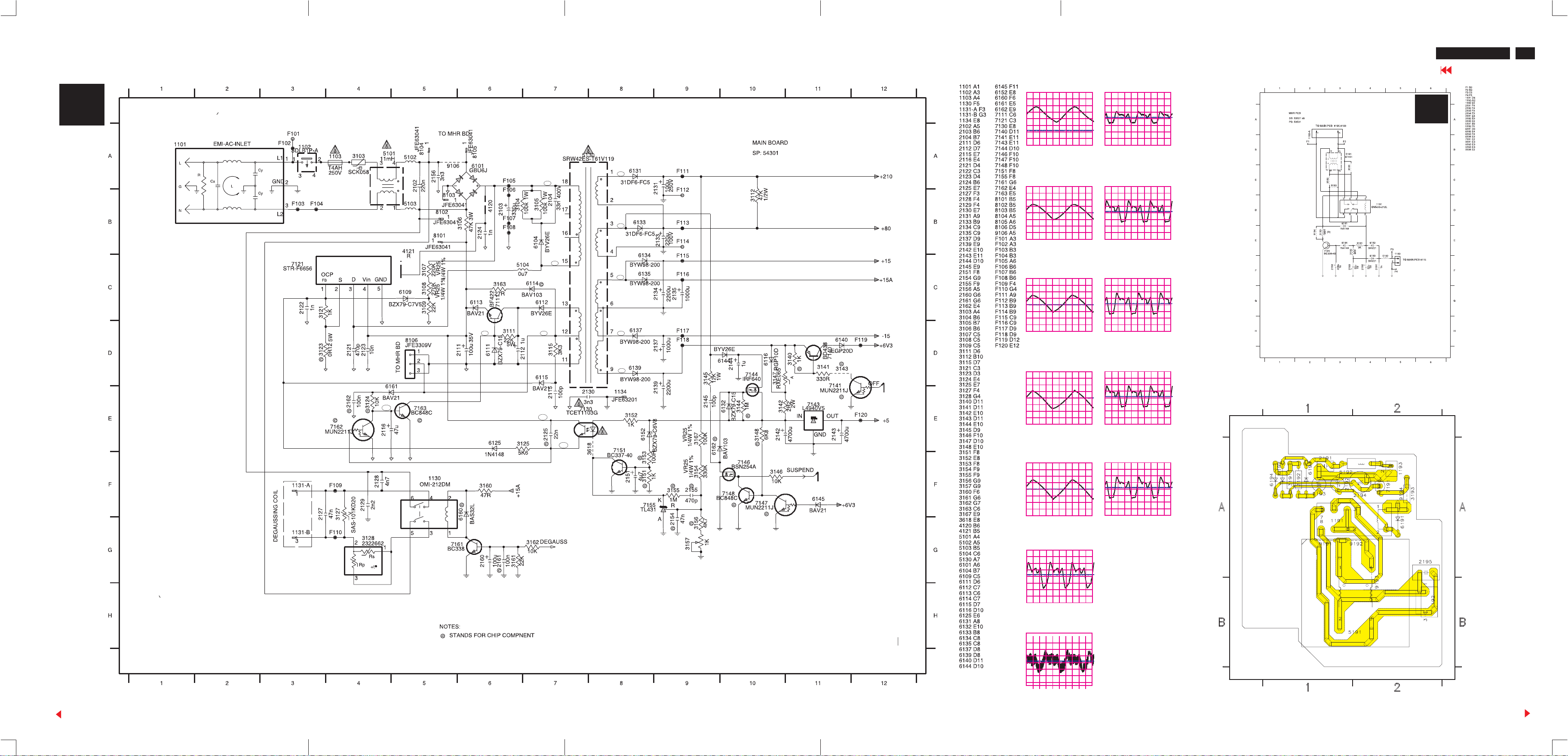
Power Schematic Diagram
201P GS3 CM25
32
37
C
Go to cover page
C1 5130-1
MHR Schematic diagram
C8 5130-12
F
10 V/div AC
2 uS/div
C1
C6
C2
C7
C3
C2 5130-3
5 V/div AC
2 uS/div
C3 5130-5
10 V/div AC
5 mS/div
C9 7111-B
5 V/div AC
5 mS/div
C10 7163-B
C10
C9
C8
C4
C5
0.5 V/div AC
2 uS/div
C4 5130-7
5 V/div AC
5 mS/div
C11 7130-4
MHR Panel PCB (F)
# GRID
C11
C12
0.5 V/div AC
2 uS/div
C5 5130-9
0.2 V/div AC
2 uS/div
C6 5130-18
5 V/div AC
5 mS/div
C12 7130-3
5 V/div AC
5 mS/div
BOARD
# REF LABEL
SIDE
# ____ _____
_________
1191 A1 B
1192 B2 B
1193 A2 B
2191 A1 B
2192 A1 B
2193 A1 B
2194 A2 B
2195 A2 B
3191 A1 B
3192 A1 B
3193 A2 B
5191 B2 B
5192 A1 B
6191 A2 B
6192 A1 B
6193 A1 B
Back
5 V/div AC
5 mS/div
C7 5130-15
10 V/div AC
5 mS/div
6194 A1 B
7191 A2 B
9191 A1 B
9192 A2 B
9193 B2 B
9194 A2 B
53531hmc
53531cus
Forward
Page 40
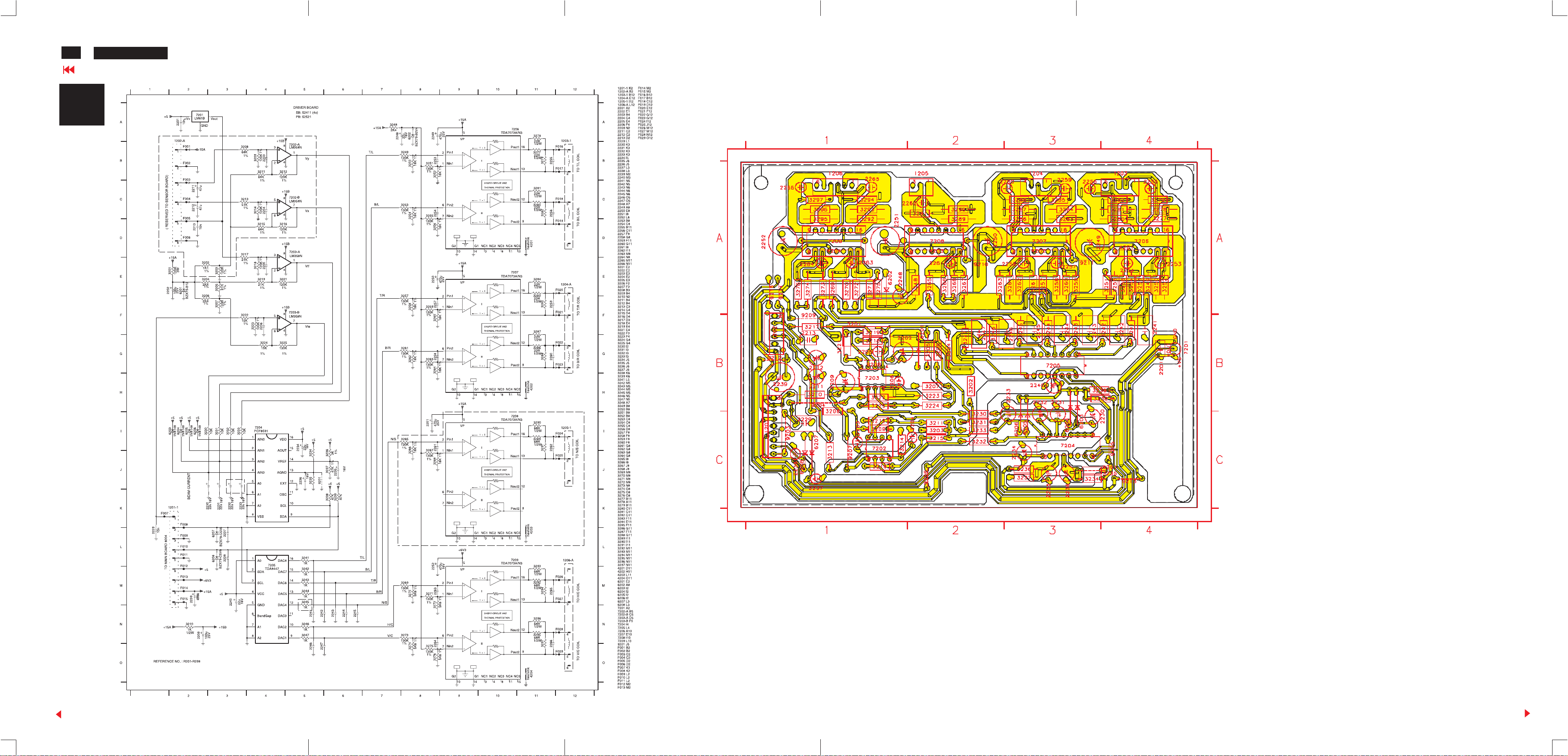
32
38
201P GS3 CM25
Go to cover page
Drive Schematic Diagram
Drive P.C.B. (D)
D
1201 C1 B
1202 B1 B
1203 A4 B
1204 A3 B
1205 A2 B
1206 A1 B
2201 B4 B
2202 B1 B
2203 C1 B
2204 C2 B
2205 B1 B
2206 B1 B
2209 B1 B
2211 B1 B
2212 B1 B
2213 B1 B
2229 C1 B
2230 C4 B
2231 B3 B
2232 B3 B
2233 B3 B
2234 C3 B
2235 C3 B
2236 C3 B
2237 C1 B
2238 C1 B
2239 B1 B
2240 B3 B
2241 B4 B
2242 B4 B
2243 B3 B
2244 B3 B
2245 B3 B
2246 B3 B
2247 B2 B
2248 A1 B
2249 A3 B
2250 A2 B
2251 A1 B
2252 A1 B
2253 A4 B
2254 A4 B
2255 A4 B
2256 A3 B
2257 A3 B
2258 A3 B
2259 A3 B
2260 A3 B
2261 A2 B
2262 A2 B
2263 A1 B
2264 A1 B
2265 A1 B
2266 A1 B
3201 B1 B
3202 B2 B
3203 C2 B
3204 B2 B
3205 B2 B
3206 B2 B
3207 B2 B
3208 B1 B
3209 C1 B
3210 B1 B
3211 C2 B
3212 C1 B
3213 C1 B
3214 C1 B
3215 C2 B
3216 C1 B
3217 B1 B
3218 B1 B
3219 B1 B
3221 B1 B
3222 B1 B
3223 B2 B
3224 B2 B
3225 B1 B
3230 C2 B
3231 C2 B
3232 C2 B
3233 C2 B
3234 C3 B
3235 C4 B
3236 C3 B
3237 C3 B
3238 B3 B
3239 B3 B
3241 B4 B
3242 B4 B
3243 B3 B
3244 B3 B
3245 B3 B
3246 B2 B
3247 B2 B
3248 A2 B
3249 A4 B
3250 A4 B
3251 A4 B
3252 A4 B
3253 A4 B
3254 A4 B
3255 A4 B
3256 A4 B
3257 A3 B
3258 A3 B
3259 A3 B
3260 A3 B
3261 A3 B
3262 A3 B
3263 A2 B
3264 A3 B
3265 A2 B
3266 A2 B
3267 A2 B
3268 A2 B
3269 A1 B
3270 A1 B
3271 A1 B
3272 A1 B
3273 A1 B
3274 A1 B
3275 A1 B
3276 A1 B
3277 A4 B
3278 A4 B
3279 A4 B
3280 A4 B
3281 A4 B
3282 A4 B
3283 A3 B
3284 A3 B
3285 A3 B
3286 A3 B
3287 A3 B
3288 A3 B
3289 A2 B
3290 A2 B
3291 A2 B
3292 A1 B
3293 A1 B
3294 A1 B
3295 A1 B
3296 A1 B
3297 A1 B
4201 A4 B
4202 A3 B
4203 A2 B
4204 A1 B
6201 B2 B
6202 A1 B
6203 C3 B
6204 C3 B
6205 C3 B
6206 C3 B
6207 C1 B
6208 C1 B
7201 B4 B
7202 C1 B
7203 B1 B
7204 C3 B
7205 B3 B
7206 A4 B
7207 A3 B
7208 A2 B
7209 A1 B
9201 C4 B
9203 C1 B
9204 B1 B
9205 C4 B
9206 C2 B
9207 C1 B
9208 B1 B
9209 B1 B
9210 A2 B
9211 A3 B
9212 B1 B
9213 C4 B
9214 A1 B
9215 A1 B
Back
Forward
Page 41
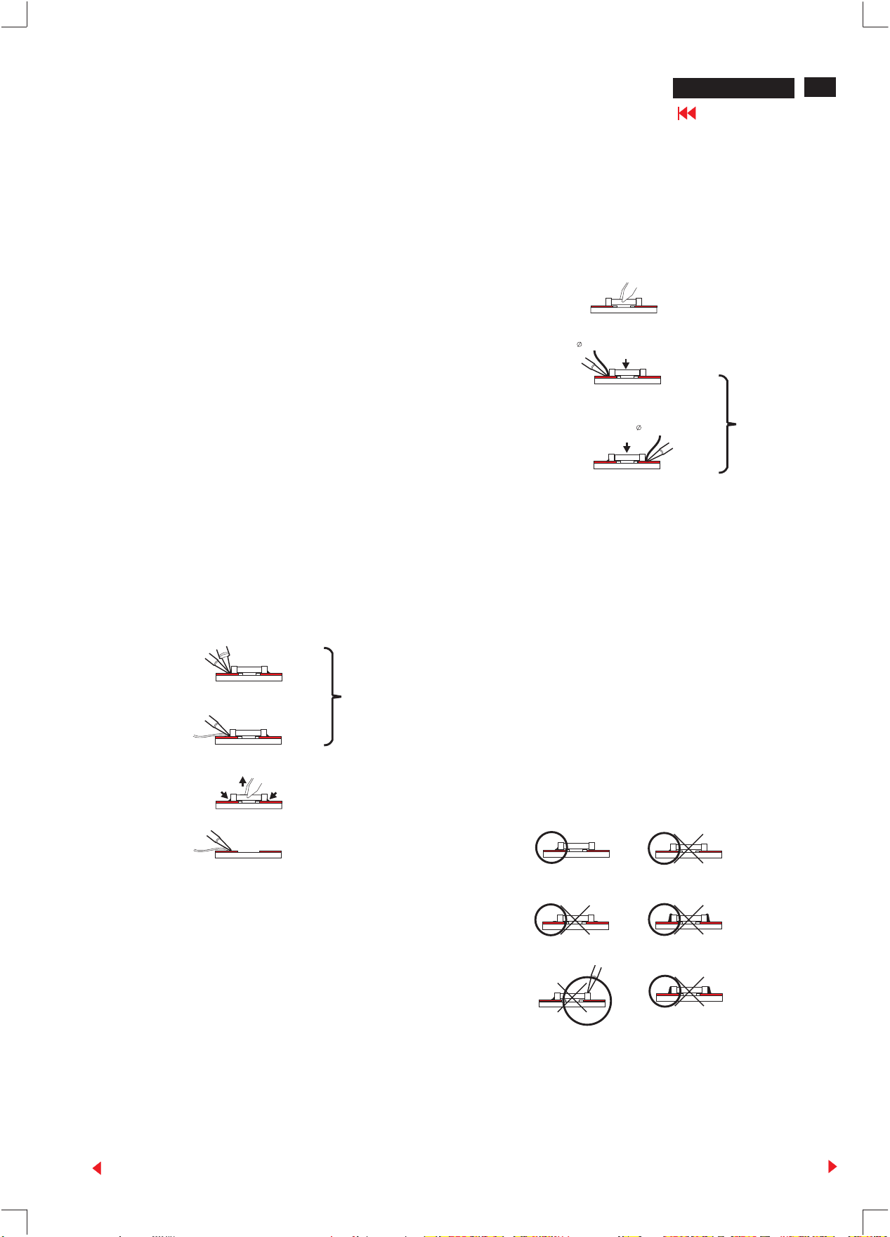
Repair TipsRepair Tips
201P GS3 CM25
Go to cover page
2639
0. Warning
All ICs and many other semi-conductors are susceptible to
electrostatic discharges (ESD). Careless handling during repair can
reduce life drastically. When repairing, make sure that you are
connected with the same potential as the mass of the unit via a wrist
wrap with resistance. Keep components and tools also at the same
potential !
1. Servicing of SMDs (Surface Mounted Devices)
1.1 General cautions on handling and storage
- Oxidation on the terminals of SMDs results in poor soldering. Do not
handle SMDs with bare hands.
- Avoid using storage places that are sensitive to oxidation such as
places with sulphur or chlorine gas, direct sunlight, high
temperatures or a high degree of humidity. The capacitance or
resistance value of the SMDs may be affected by this.
- Rough handling of circuit boards containing SMDs may cause
damage to the components as well as the circuit boards. Circuit
boards containing SMDs should never be bent or flexed. Different
circuit board materials expand and contract at different rates when
heated or cooled and the components and/or solder connections
may be damaged due to the stress. Never rub or scrape chip
components as this may cause the value of the component to
change. Similarly, do not slide the circuit board across any surface.
1.2 Removal of SMDs
- Heat the solder (for 2-3 seconds) at each terminal of the chip. By
means of litz wire and a slight horizontal force, small components
can be removed with the soldering iron. They can also be removed
with a solder sucker (see Fig. 1A)
Fig. 1
DISMOUNTING
VACUUM PISTON
SOLDERING
IRON
e.g. WELLER
SOLDER TIP PT -H7
SOLDERING
IRON
SOLDER WICK
4822 321 40042
HEATING
4822 395 10159
A
e.g. A PAIR OF TWEEZERS
HEATING
B
solder the component on one side. Ensure that the component is
Positioned correctly on the solder lands (see Fig.2A).
- Next complete the soldering of the terminals of the component (see
Fig. 2B).
Fig. 2
MOUNTING
e.g. A PAIR OF TWEEZERS
A
SOLDER
SOLDERING
IRON
SOLDERING TIME
< 3 sec/side
0.5 - 0.8 mm
PRESURE
PRESURE
SOLDER
0.5 - 0.8 mm
SOLDERING
IRON
B
2. Caution when attaching SMDs
- When soldering the SMD terminals, do not touch them directly with
the soldering iron. The soldering should be done as quickly as
possible, care must be taken to avoid damage to the terminals of
the SMDs themselves.
- Keep the SMD's body in contact with the printed board when
soldering.
- The soldering iron to be used (approx. 30W)should preferably be
equipped with a thermal control (soldering temperature: 225 to 250
o
C).
- Soldering should not be done outside the solder land.
- Soldering flux (of rosin) may be used, but should not be acidic.
- After soldering, let the SMD cool down gradually at room
temperature.
- The quantity of solder must be proportional to the size of the solder
land. If the quantity is too great, the SMD might crack or the solder
lands might be torn loose from the printed board (see Fig. 3).
Examples
Fig. 3
SOLDERING
IRON
SOLDER WICK
C
- While holding the SMD with a pair of tweezers, take it off gently
using the soldering iron's heat applied to each terminal (see Fig. 1
B).
- Remove the excess solder on the solder lands by means of litz wire
or a solder sucker (see Fig. 1C).
1.3 Caution on removal
- When handling the soldering.iron. use suitable pressure and be
careful.
- When removing the chip, do not use undue force with the pair of
tweezers.
- The soldering iron to be used (approx. 30 W) should
equipped with a thermal control (soldering temperature: 225 to 250
o
C).
preferably be
- The chip, once removed, must never be reused.
1.4 Attachment of SMDs
- Locate the SMD on the solder lands by means of tweezers and
Back
RIGHT
SOLDERING
IRON
Forward
Page 42
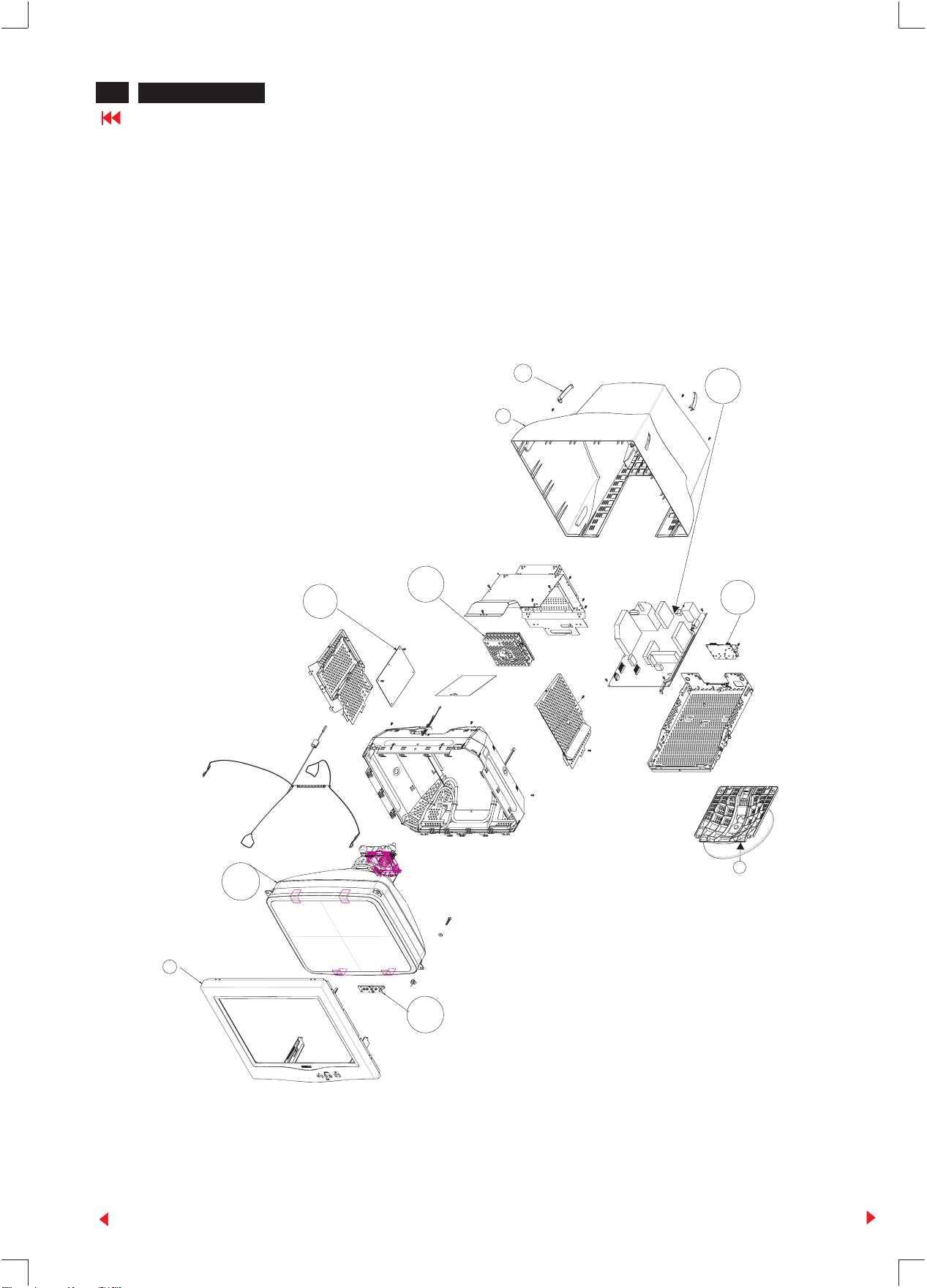
COMPAQ V1000
40
201P GS3 CM25
Go to cover page
Exploded View
3138 178 06950
DRIVE PCB ASSY 5252
3138 107 98870
BACK COVER ASSY (201P)
3138 178 08870
VIDEO PCB ASSY 5292
1162
1164
3138 104 50410
SCREW COVER
49
2
3138 178 55390
MAIN PCB ASSY 5240
1160
3138 178 04700
TERMINAL PCB ASSY
1161
9322 160 42682
CRT 21" M51LRY 22X62 0.24
1051
3138 107 98860
FRONT CABINET ASSY (201P)
1
Back
3138 107 98480
3
PEDESTAL ASSY
1163
3138 178 07120
CONTROL PCB ASSY 5230
Forward
Page 43
Recommanded Parts List
201P GS3 CM 25
Go to cover page
41
Model : 201P10/00
ITEM CODE NUMBER DESCRIPTION
1 3138 107 98860 FRONT CABINET ASSY (201P)
2 3138 107 98870 BACK COVER ASSY (201P)
3 3138 107 98480 PEDESTAL ASSY
4 3138 107 98750 KNOB ASSY
44 3138 104 49470 BASE
46 3138 104 49890 KNOB-OSD
47 3138 104 49880 KNOB-POWER
48 3138 104 50670 LENS-POWER
49 3138 104 50410 SCREW COVER
53 3138 104 49460 SWIVEL
601 3138 117 02140 E-D.F.U. ASSY (P SERIES)
450 3138 106 57450 CARTON
451 3138 106 57100 CUSHION - TOP FRONT
452 3138 106 57110 CUSHION - TOP REAR
453 3138 106 57120 CUSHION - BOTTOM
454 3138 106 45300 P.E. BAG
1053 2438 070 98118 MAINS CORD(220V)-1.5M
1054 3138 168 74450 I/F CABLE
1103 2422 086 00208 FUSE T4AH 250V
1160 3138 178 55390 201P-M(MHR)MAIN PCB ASSY
1161 3138 178 04700 TERMINAL PCB ASSY
1162 3138 178 08870 VIDEO PCB ASSY 5292
1163 3138 178 07120 CONTROL PCB ASSY 5230
1164 3138 178 06950 DRIVE PCB ASSY 5252
1167 3138 178 53330 109P2-MHR PCB ASSY 5353
5671 3138 138 31810 L.O.T. AT2097/26B
7001 9322 142 60682 IC AN5870K 30P
7121 9322 145 76682 IC STRF6656 (LF1352)
7130 9322 140 14667 PHOTOCOUPLER TCET1103G 4P
7143 9322 092 00687 IC L4940V5 3P
7155 9337 711 00686 IC TL431CLPRP 3P
7201 9322 139 99682 IC LM61BIZ 3P
7203 9333 935 10602 IC LM358N 8P (PHILIPS)
7204 9337 681 30112 IC PCF8591P 16P
7205 9352 298 30112 IC TDA8447/N1 16P
7206 9351 920 50112 IC TDA7073A/N3 16P
7301 9352 644 29112 IC P83C380AER/079 42P
1265 3138 178 08880 EEPROM IC ASSY 7336
7351 9352 608 01112 IC PDIUSBD11N 16P
7363 9334 006 10682 IC MC7812CT 3P
7364 9339 208 10682 IC L7808CV 3P
7404 9332 826 60652 IC HEF4053BP 16P
7421 9352 623 32112 IC TDA4856/V2 32P
7491 9322 098 98682 IC ST24LC21BB6 8P
7541 9322 118 29687 FET POW 2SJ448
7567 9319 002 34682 IC STV9379 7P
7651 9322 121 52682 IC L4990A 16P
7672 9319 001 79687 IRF740 POWER MOS-FET
7673 9322 124 60687 FET POW STU8NA80 (ST00) L
7675 9322 106 11676 IC LE33CZ-AP 3P
7701 9337 148 40653 IC 74HC4053D
7704 9322 128 48682 IC M52742SP 36P
7708 9337 140 40653 IC 74HCT86D 14P
7711 9340 551 51127 IC CR6927L 12P
7727 9334 530 30682 IC MC7905CT 3P
7801 9338 369 30668 IC TL072CDR SO-8P
7806 9338 516 60118 IC PCF8574AT SO-16P
7855 8238 274 35560 IC LSC4588P2
7859 9337 144 20653 IC 74HC4066D SO-14P
7891 8238 274 34990 LM61BIM (SOT-23)
Model : 201P10/74
ITEM CODE NUMBER DESCRIPTION
450 3138 106 58200 CARTON
1053 3138 118 75010 MAINS CORD(120v)
Remark: Item 450 and item 1053 are the
differences between 201P10/00
and 201P10/74.
Back
Forward
Page 44

201P GS3 CM 25
42
Go to cover page
Spare Parts list
ITEM CODENUMBER DESCRIPTION
1 3138 107 98860 FRONT CABINET ASSY (201P)
2 3138 107 98870 BACK COVER ASSY (201P)
3 3138 107 98480 PEDESTAL ASSY
4 3138 107 98750 KNOB ASSY
24 3138 107 99070 BOTTOM PLATE ASSY (201P)
44 3138 104 49470 BASE
46 3138 104 49890 KNOB-OSD
47 3138 104 49880 KNOB-POWER
48 3138 104 50670 LENS-POWER
49 3138 104 50410 SCREW COVER
53 3138 104 49460 SWIVEL
55 3138 104 49830 POWER LEVEL
56 3138 104 49480 FOOT RUBBER
57 3138 104 40570 HOUSING COVER
58 3138 104 52590 PLASTIC RIVET
178 3138 105 39450 SETTING UP GUIDE
601 3138 117 02140 E-D.F.U. ASSY (P SERIES)
450 3138 106 57450 CARTON
451 3138 106 57100 CUSHION - TOP FRONT
452 3138 106 57110 CUSHION - TOP REAR
453 3138 106 57120 CUSHION - BOTTOM
454 3138 106 45300 P.E. BAG
1051 9322 160 42682 CRT 21" M51LRY 22X62 0.24
1053 2438 070 98118 MAINS CORD
1054 3138 168 74450 I/F CABLE
1057 3138 178 75560 1.5M USB CABLE
1058 2422 549 42025 IND FXD BEAD EMI 100MHZ 100E B
1061 3138 168 76050 DEGASSING COIL 62-9908-10
1063 3138 168 76020 CORNER COIL 62-9908-12
1064 3138 168 76030 CORNER COIL 62-9908-13
1101 3138 168 73820 AC INLET ASSY EMI FILTER
1102 2438 128 00107 POWER SWITCH
1103 2422 086 00208 FUSE T4AH 250V
1130 2438 132 00056 RELAY - OMI-SS-212DM
1131 2438 025 00208 WAFER 2P
1160 3138 178 55390 201P-M(MHR)MAIN PCB ASSY
1161 3138 178 04700 TERMINAL PCB ASSY
1162 3138 178 08870 VIDEO PCB ASSY 5292
1163 3138 178 07120 CONTROL PCB ASSY 5230
1164 3138 178 06950 DRIVE PCB ASSY 5252
1167 3138 178 53330 109P2-MHR PCB ASSY 5353
1191 2438 031 00048 CON BM H 3P M 2.5 625/626 B
1191 2411 121 02038 RELAY OMI-SS-212L
1192 3138 168 76340 3-1p wafer
1193 3138 168 72030 2P WAFER M24262 (VERT)
1201 2438 031 00068 CON BM V 9P M 2.5 625/635 B
1203 3138 168 72960 CON BM H 5P M 2.5 (61145)
1204 2438 031 00223 CON BM V 4P M 2.50 61144 B
1206 3138 168 73080 CON BM H 6P M 2.5 (61146)
1265 3138 178 08880 EEPROM IC ASSY 7336
1286 3138 168 73680 BNC CONNECTOR ASSY
1293 2438 031 00167 CON BM IC V 42P F 1.778 DIL B
1301 2438 543 00064 CRYSTAL-12MHZ
1302 2438 031 00227 UP-STREAM PORT CONNECTOR B
1303 2438 543 00064 CRYSTAL-12MHZ
1311 2438 031 00066 CON BM V 7P M 2.5 625/635 B
1501 3138 100 20990 CONNECTOR 4P 2.35 DIA J101
1502 2438 031 00224 CON BM V 2P M 2.5 61142 B
1703 2438 032 01009 CONNECTOR 1P 1.54 DIA
1705 2438 031 00056 CON BM H 10P M 2.5 625/626 B
1706 2438 031 00057 CON BM H 11P M 2.5 625/626 B
1710 2422 500 80055 CRT SCKT CVT3280 11P DIA 22.5
1712 3138 178 77650 1P WAFER 2.0 DIA
1891 2438 128 00196 SWI TACT H EQU. TO 5 GY 160G
1892 2438 128 00196 SWI TACT H EQU. TO 5 GY 160G
1893 2438 128 00196 SWI TACT H EQU. TO 5 GY 160G
1894 2438 128 00196 SWI TACT H EQU. TO 5 GY 160G
1895 2438 128 00196 SWI TACT H EQU. TO 5 GY 160G
2001 2038 035 50227 ELECAP SS 220U 10V 6*7T
2002 2038 035 50312 ELCAP SS 220UF 16V
2003 2038 035 00037 ELCAP SM 16V 47U PM20 2E T
2004 2038 035 00037 ELCAP SM 16V 47U PM20 2E T
2005 2038 035 00037 ELCAP SM 16V 47U PM20 2E T
Back
ITEM CODENUMBER DESCRIPTION
2007 2038 035 00037 ELCAP SM 16V 47U PM20 2E T
2008 2238 910 15649 CER2 0805 X7R 25V 100N CO
2010 2238 910 15649 CER2 0805 X7R 25V 100N CO
2011 2038 035 00037 ELCAP SM 16V 47U PM20 2E T
2013 2038 035 00037 ELCAP SM 16V 47U PM20 2E T
2017 2238 910 15649 CER2 0805 X7R 25V 100N CO
2018 2238 861 15109 CAP 10PF 0805 SMD
2019 2238 861 15109 CAP 10PF 0805 SMD
2020 2238 861 15109 CAP 10PF 0805 SMD
2021 2238 861 15109 CAP 10PF 0805 SMD
2023 2038 035 50227 ELECAP SS 220U 10V 6*7T
2025 2038 035 50227 ELECAP SS 220U 10V 6*7T
2027 2038 035 50227 ELECAP SS 220U 10V 6*7T
2031 2238 861 15229 CAP 22PF 0805 SMD NPO
2032 2238 861 15229 CAP 22PF 0805 SMD NPO
2033 2238 861 15229 CAP 22PF 0805 SMD NPO
2034 2238 861 15229 CAP 22PF 0805 SMD NPO
2035 2238 910 15649 CER2 0805 X7R 25V 100N CO
2036 2238 910 15649 CER2 0805 X7R 25V 100N CO
2102 2020 307 90011 ACROSS LINE CAP 250V 220N PM10
2103 2038 035 00042 ELCAP LXK 400V S 330U PM 20
2104 8238 274 37251 CAP MEF 400V 33N
2111 2038 031 55101 ELCAP S 35V 100UF PM20 2E
2112 2038 035 50202 ELCAP SH 250V S 1U PM20 A
2115 2020 558 90542 CER2 DC RR 1KV S 100P PM10 A
2116 2038 031 45479 ELCAP VT 25V 47UF PM20 2E T
2121 2020 558 90555 CCAP DC RR 1KV S 470P K A
2122 2020 558 90557 CERC RR 1KVDC 1N PM10
2123 2238 580 16627 CER2 0805 X7R 50V 10N PM10 R
2124 2020 557 90151 CERC DC 500V 1N0 PM10
2125 2238 580 15641 SMD C0805 22N 63V PM10 X710 R
2127 2222 347 41473 POLCAP S 250V 47N PM10 6E
2128 2020 554 90139 CERSAF NSB 250V S 4N7 PM20 B
2129 2020 554 90127 CERSAF NSA 250V S 2N2 PM20 B
2130 2020 554 90149 CERSAF NSA 250V S 3N3 PM20
2131 2038 035 00081 ELCAP SX 250V S 100U PM20 B
2133 2038 035 00099 ELCAP SX 100V S 220U PM20 B
2134 2038 035 00079 ELCAP SX 25V S 2200U PM20 B
2135 2038 035 00078 ELCAP SX 25V S 1000U PM20 B
2137 2038 035 00078 ELCAP SX 25V S 1000U PM20 B
2139 2038 035 00056 ELCAP 2200UF 16V SX PM20
2142 2038 017 00325 ELCAP VZ 10V S 4700U PM20 B
2143 2038 017 00325 ELCAP VZ 10V S 4700U PM20 B
2144 2038 031 95005 ELCAP S 160V 1UF PM20 2E T
2145 2020 558 90542 CER2 DC RR 1KV S 100P PM10 A
2151 2038 031 65478 ELCAP 4UF7 50V PM20 VT A
2154 2238 910 15645 CAP 47NF SMD 0805 X7R
2155 2238 861 15471 CMC 0805 NPO 470P 50V J
2156 2020 554 90149 CERSAF NSA 250V S 3N3 PM20
2160 2038 034 52101 ELCAP S 10V 100UF PM20 2E T
2161 2238 910 15649 CER2 0805 X7R 25V 100N CO
2162 2238 910 15649 CER2 0805 X7R 25V 100N CO
2192 2038 302 00203 MEF CAP 630V 47N 6E PM10
2192 2038 034 56229 ELCAP S 50V 22UF PM20 2E T
2193 2038 034 56229 ELCAP S 50V 22UF PM20 2E T
2194 2038 034 53221 ELCAP S 16V 220UF PM20 2E
2201 2252 325 12103 CERC CAP 50V 10N X7R 2E
2202 2038 034 54101 ELCAP S 25V 100UF PM20 2E
2209 2038 034 54101 ELCAP S 25V 100UF PM20 2E
2213 2252 325 12103 CERC CAP 50V 10N X7R 2E
2229 2252 325 12103 CERC CAP 50V 10N X7R 2E
2230 2038 034 53229 ELCAP S 16V 22UF PM20 2E
2231 2038 034 53229 ELCAP S 16V 22UF PM20 2E
2234 2038 034 53229 ELCAP S 16V 22UF PM20 2E
2239 2038 031 42471 ELCAP 470UF 25V PM20 2E 105C B
2240 2038 034 53229 ELCAP S 16V 22UF PM20 2E
2248 2038 034 53229 ELCAP S 16V 22UF PM20 2E
2249 2038 034 24471 ELCAP S 25V 470UF PM20 2E
2250 2038 034 24471 ELCAP S 25V 470UF PM20 2E
2251 2038 034 24471 ELCAP S 25V 470UF PM20 2E
2252 2038 034 23471 ELCAP S 16V 470UF PM20 2E B
2302 2238 580 16614 CER2 0805 X7R 50V 1N PM10
2304 2038 302 50095 MEF CAP 100V 100N PM10 2E
2306 2038 034 56109 ELCAP S 50V 10UF PM20 2E
2309 2238 861 15339 CAP 33PF 0805 SMD NPO
2310 2238 861 15339 CAP 33PF 0805 SMD NPO
Forward
Page 45

Spare Parts list
201P GS 3 CM25
Go to cover page
43
ITEM CODENUMBER DESCRIPTION
2518 2038 302 50095 MEF CAP 100V 100N PM10 2E
2519 2038 302 50095 MEF CAP 100V 100N PM10 2E
2520 2038 302 50095 MEF CAP 100V 100N PM10 2E
2542 2038 302 00155 MEF CAP 250V 100N PM10
2543 2038 035 00048 ELCAP SEK 250V S 100U PM20 B
2544 2020 558 90561 CERC CAP RR 2KV 220P PM10 B
2545 2238 910 15649 CER2 0805 X7R 25V 100N CO
2546 2238 910 15649 CER2 0805 X7R 25V 100N CO
2551 2038 031 45479 ELCAP VT 25V 47UF PM20 2E T
2552 2038 031 45479 ELCAP VT 25V 47UF PM20 2E T
2553 2038 301 00164 CAP PP PPN 250V S 150N PM5 B
2555 2038 301 00195 CAP PPN 120N 250V PM5 9E
2566 2038 031 65109 ELCAP VT 50V 10UF PM20 2E
2567 2038 031 42471 ELCAP 470UF 25V PM20 2E 105C B
2568 2038 034 55101 ELCAP S 35V 100UF PM20 2E
2569 2020 552 90607 CERC DC NPO 50V 220P PM5 2E T
2576 2038 302 50093 MEF CAP 100V 22N PM10 2E
2577 2038 031 42471 ELCAP 470UF 25V PM20 2E 105C B
2578 2038 302 50095 MEF CAP 100V 100N PM10 2E
2579 2038 302 50099 POLCAP 100V 470N PM10 2E
2586 2038 302 50212 POLCAP 100V 100N PM5 2E T
2587 2038 302 50095 MEF CAP 100V 100N PM10 2E
2588 2038 302 50095 MEF CAP 100V 100N PM10 2E
2589 2038 302 50095 MEF CAP 100V 100N PM10 2E
2601 2020 558 90561 CERC CAP RR 2KV 220P PM10 B
2602 2252 712 14116 CERC CAP 150P 2KV Y5R TYPE K 2E T
2603 2020 558 90557 CERC RR 1KVDC 1N PM10
2608 2235 559 00099 CERC CAP 2KV 10N PM20 4E
2611 2038 034 54479 ELCAP S 25V 47UF PM20 2E T
2612 2238 910 15649 CER2 0805 X7R 25V 100N CO
2613 2038 034 56479 ELCAP S 50V 47UF PM20 2E T
2621 2038 301 00188 CAP PP PPN 250V S 68N PM5 6E B
2623 2038 301 00225 MPS CAP 270N 250V PM5
2624 2038 301 00304 MPS CAP 560N/250V PM5 7E
2627 2038 301 00225 MPS CAP 270N 250V PM5
2632 2038 301 00205 CAP PP DTW 250V 82N PM5
2635 2038 301 00311 MPS CAP 1U 250V PM5 9E
2636 2038 301 00158 CAP MPP MPS 250V S 1U8 PM5 B
2651 2038 034 56108 ELCAP S 50V 1UF PM20 2E T
2652 2238 580 16616 CER2 0805 X7R 63V 1N5 PM10 R
2653 2238 580 16621 MLCC 0805 X7R 3N3 K 4B 9
2655 2038 301 50151 CAP PP PPN 100V S 10N PM2 B
2656 2038 031 45221 ELCAP S 25V 220UF PM20 2E T
2657 2238 580 16615 CER2 0805 X7R 63V 1N2 PM10 R
2658 2238 780 19858 CER2 0805 Y5V 16V 470N P8020 R
2659 2038 034 54479 ELCAP S 25V 47UF PM20 2E T
2660 2238 780 19858 CER2 0805 Y5V 16V 470N P8020 R
2661 2238 780 19858 CER2 0805 Y5V 16V 470N P8020 R
2671 2038 031 92003 ELCAP S 250V 33UF PM20 2E
2672 2238 910 15649 CER2 0805 X7R 25V 100N CO
2673 2020 558 90562 CERC RB 2KVDC 330PF
2681 2238 580 16618 CAP 2NF2 0805 SMD X7R T
2682 2038 035 00081 ELCAP SX 250V S 100U PM20 B
2683 2038 301 00174 CAP PP PPN 630V S 4N7 PM5 A
2684 2222 347 41473 POLCAP S 250V 47N PM10 6E
2685 2038 034 53479 ECAP S 16V 47UF M 2E T
2686 2020 558 90557 CERC RR 1KVDC 1N PM10
2691 2222 347 41473 POLCAP S 250V 47N PM10 6E
2693 2038 302 00226 CAP MPOL 100V S 1U8 PM5 B
2694 2038 302 50212 POLCAP 100V 100N PM5 2E T
2701 2038 031 65338 CAP VT3.3U50V2 5*11 2E(T)
2702 2238 580 16614 CER2 0805 X7R 50V 1N PM10
2703 2238 910 15649 CER2 0805 X7R 25V 100N CO
2704 2238 580 16627 CER2 0805 X7R 50V 10N PM10 R
2706 2222 861 12271 CER1 0805 NP0 50V 270P PM5
2707 2238 580 16627 CER2 0805 X7R 50V 10N PM10 R
2708 2238 910 15649 CER2 0805 X7R 25V 100N CO
2709 2238 861 15339 CAP 33PF 0805 SMD NPO
2710 2238 861 15279 CAP 27PF 0805 SMD NPO
2711 2238 861 15339 CAP 33PF 0805 SMD NPO
2712 2238 910 15649 CER2 0805 X7R 25V 100N CO
2713 2038 031 92015 ELCAP VT 160V S 22U PM20 B
2714 2252 326 13103 CER CAP X7R 100V 10N K 2E T
2715 2222 691 10229 MINATURE PLATE CAP 22P 500V
NPO 2E T
ITEM CODENUMBER DESCRIPTION
2717 2038 035 22801 ECAP NP 1U 160V 105C NK
2718 2038 035 50202 ELCAP SH 250V S 1U PM20 A
2719 2422 549 44346 SPARK GAP DSP-201m
2721 2222 780 19763 CMC 0805 Y5V 1U M 16V
2722 2238 910 15649 CER2 0805 X7R 25V 100N CO
2723 2222 780 19763 CMC 0805 Y5V 1U M 16V
2724 2238 910 15649 CER2 0805 X7R 25V 100N CO
2725 2222 780 19763 CMC 0805 Y5V 1U M 16V
2726 2238 910 15649 CER2 0805 X7R 25V 100N CO
2727 2238 910 15649 CER2 0805 X7R 25V 100N CO
2728 2222 780 19763 CMC 0805 Y5V 1U M 16V
2731 2038 031 65338 CAP VT3.3U50V2 5*11 2E(T)
2732 2238 580 16614 CER2 0805 X7R 50V 1N PM10
2733 2038 031 45471 ELCAP 470UF 25V PM20 2E 105C T
2734 2238 910 15649 CER2 0805 X7R 25V 100N CO
2737 2222 861 12271 CER1 0805 NP0 50V 270P PM5
2738 2238 580 16627 CER2 0805 X7R 50V 10N PM10 R
2739 2238 910 15649 CER2 0805 X7R 25V 100N CO
2740 2238 861 15339 CAP 33PF 0805 SMD NPO
2741 2238 861 15279 CAP 27PF 0805 SMD NPO
2742 2238 861 15339 CAP 33PF 0805 SMD NPO
2743 2238 910 15649 CER2 0805 X7R 25V 100N CO
2744 2252 326 13103 CER CAP X7R 100V 10N K 2E T
2745 2222 691 10229 MINATURE PLATE CAP 22P 500V
NPO 2E T
2747 2038 035 22801 ECAP NP 1U 160V 105C NK
2748 2038 035 50202 ELCAP SH 250V S 1U PM20 A
2749 2422 549 44346 SPARK GAP DSP-201m
2751 2238 910 15649 CER2 0805 X7R 25V 100N CO
2752 2238 910 15649 CER2 0805 X7R 25V 100N CO
2753 2238 910 15649 CER2 0805 X7R 25V 100N CO
2761 2038 031 65338 CAP VT3.3U50V2 5*11 2E(T)
2762 2238 580 16614 CER2 0805 X7R 50V 1N PM10
2763 2238 910 15649 CER2 0805 X7R 25V 100N CO
2764 2252 611 08216 DISC CAP Y5P 1KV 220PF K 2E T
2765 2222 861 12271 CER1 0805 NP0 50V 270P PM5
2766 2238 580 16627 CER2 0805 X7R 50V 10N PM10 R
2767 2238 910 15649 CER2 0805 X7R 25V 100N CO
2768 2252 326 13103 CER CAP X7R 100V 10N K 2E T
2769 2238 861 15339 CAP 33PF 0805 SMD NPO
2770 2238 861 15279 CAP 27PF 0805 SMD NPO
2771 2238 861 15339 CAP 33PF 0805 SMD NPO
2772 2038 031 45101 ECAP S 25V 100UF M 2E T
2773 2238 910 15649 CER2 0805 X7R 25V 100N CO
2774 2222 743 90061 CER2 DC Z5U 2KV S 10N PM20 B
2776 2038 035 22801 ECAP NP 1U 160V 105C NK
2777 2038 035 50202 ELCAP SH 250V S 1U PM20 A
2778 2422 549 44346 SPARK GAP DSP-201m
2790 2238 910 15649 CER2 0805 X7R 25V 100N CO
2791 2238 910 15649 CER2 0805 X7R 25V 100N CO
2792 2238 910 15649 CER2 0805 X7R 25V 100N CO
2796 2038 035 50202 ELCAP SH 250V S 1U PM20 A
2801 2238 580 16627 CER2 0805 X7R 50V 10N PM10 R
2802 2238 861 15101 CER2 0805 NPO 50V 100P
2803 2238 910 15649 CER2 0805 X7R 25V 100N CO
2804 2238 861 15181 MLCC 0805 NPO 180PF J 4B 9
2805 2238 910 15649 CER2 0805 X7R 25V 100N CO
2806 2238 910 15649 CER2 0805 X7R 25V 100N CO
2807 2238 910 15649 CER2 0805 X7R 25V 100N CO
2811 2038 035 50202 ELCAP SH 250V S 1U PM20 A
2812 2238 580 16614 CER2 0805 X7R 50V 1N PM10
2813 2238 580 16621 MLCC 0805 X7R 3N3 K 4B 9
2814 2238 910 15649 CER2 0805 X7R 25V 100N CO
2815 2238 910 15649 CER2 0805 X7R 25V 100N CO
2821 2238 580 16614 CER2 0805 X7R 50V 1N PM10
2822 2238 580 16621 MLCC 0805 X7R 3N3 K 4B 9
2831 2238 580 16614 CER2 0805 X7R 50V 1N PM10
2832 2238 580 16621 MLCC 0805 X7R 3N3 K 4B 9
2833 2038 031 65479 ELCAP S 50V 47UF PM20 2E T
2850 2238 910 15649 CER2 0805 X7R 25V 100N CO
2851 2038 031 65109 ELCAP VT 50V 10UF PM20 2E
2852 2238 580 16627 CER2 0805 X7R 50V 10N PM10 R
2853 2038 031 45471 ELCAP 470UF 25V PM20 2E 105C T
2854 2238 580 16627 CER2 0805 X7R 50V 10N PM10 R
Back
Forward
Page 46

201P GS 3 CM25
44
Go to cover page
Spare Parts list
ITEM CODENUMBER DESCRIPTION
2855 2038 031 35101 ELCAP VT 16V 100UF PM20 2E T
2856 2238 910 15649 CER2 0805 X7R 25V 100N CO
2857 2222 910 19856 CER2 0805 Y5V 25V 330N P8020 R
2858 2238 580 15641 SMD C0805 22N 63V PM10 X710 R
2859 2238 861 15221 MLCC 0850 NPO 220PF J 4B 9
2860 2238 861 15221 MLCC 0850 NPO 220PF J 4B 9
2861 2238 861 15101 CER2 0805 NPO 50V 100P
2863 2038 031 45101 ECAP S 25V 100UF M 2E T
2864 2038 031 45479 ELCAP VT 25V 47UF PM20 2E T
2865 2238 910 15649 CER2 0805 X7R 25V 100N CO
2866 2238 861 15229 CAP 22PF 0805 SMD NPO
2867 2238 580 16627 CER2 0805 X7R 50V 10N PM10 R
2868 2238 861 15229 CAP 22PF 0805 SMD NPO
2870 2238 861 15229 CAP 22PF 0805 SMD NPO
2871 2238 861 15229 CAP 22PF 0805 SMD NPO
2872 2038 031 45479 ELCAP VT 25V 47UF PM20 2E T
2873 2238 910 15649 CER2 0805 X7R 25V 100N CO
2874 2238 910 15649 CER2 0805 X7R 25V 100N CO
2875 2238 910 15649 CER2 0805 X7R 25V 100N CO
2876 2222 691 10229 MINATURE PLATE CAP 22P 500V
NPO 2E T
2877 2252 602 14416 CERC CAP DC 2KV 470P PM10 X7R
2878 2020 557 90151 CERC DC 500V 1N0 PM10
2879 2038 031 45109 ELCAP VT 10U 25V 2E M T
2880 2238 910 15649 CER2 0805 X7R 25V 100N CO
2881 2038 031 45479 ELCAP VT 25V 47UF PM20 2E T
2882 2238 910 15649 CER2 0805 X7R 25V 100N CO
2883 2238 910 15649 CER2 0805 X7R 25V 100N CO
2884 2038 031 35331 ELCAP S 16V 330UF PM20 2E T
2885 2238 910 15649 CER2 0805 X7R 25V 100N CO
2886 2038 031 45479 ELCAP VT 25V 47UF PM20 2E T
2887 2222 780 19763 CMC 0805 Y5V 1U M 16V
2889 2038 302 50095 MEF CAP 100V 100N PM10 2E
2890 2038 035 50202 ELCAP SH 250V S 1U PM20 A
2891 2238 910 15649 CER2 0805 X7R 25V 100N CO
2891 2038 302 50166 MEF CAP 400V 10N PM10 2E T
2892 2238 910 15649 CER2 0805 X7R 25V 100N CO
2892 2238 861 15229 CAP 22PF 0805 SMD NPO
2893 2238 910 15649 CER2 0805 X7R 25V 100N CO
2893 2238 861 15229 CAP 22PF 0805 SMD NPO
2894 2238 580 16627 CER2 0805 X7R 50V 10N PM10 R
2894 2238 861 15229 CAP 22PF 0805 SMD NPO
2895 2238 580 16627 CER2 0805 X7R 50V 10N PM10 R
2895 2238 861 15229 CAP 22PF 0805 SMD NPO
2896 2238 910 15649 CER2 0805 X7R 25V 100N CO
2897 2238 910 15649 CER2 0805 X7R 25V 100N CO
2898 2238 861 15101 CER2 0805 NPO 50V 100P
2899 2238 861 15101 CER2 0805 NPO 50V 100P
2900 2238 580 16623 MLCC 0805 X7R 4N7F K 4B 9
2901 2252 602 14216 CERCAP DC 2KV 220P K X7R T
3001 2322 730 61222 RST SM 0805 RC11 2K2 PM5 R
3004 2322 730 61222 RST SM 0805 RC11 2K2 PM5 R
3006 2322 730 61479 RES 47R 0805 SMD RC-11 T
3007 2322 734 67509 RST SM 0805 RC11 75R PM1 T
3008 2322 730 61479 RES 47R 0805 SMD RC-11 T
3009 2322 734 67509 RST SM 0805 RC11 75R PM1 T
3010 2322 730 61479 RES 47R 0805 SMD RC-11 T
3011 2322 734 67509 RST SM 0805 RC11 75R PM1 T
3012 2322 730 61471 RST SM 0805 RC11 470R PM5 R
3013 2322 730 61471 RST SM 0805 RC11 470R PM5 R
3014 2322 730 61471 RST SM 0805 RC11 470R PM5 R
3015 2322 730 61471 RST SM 0805 RC11 470R PM5 R
3016 2322 730 61479 RES 47R 0805 SMD RC-11 T
3017 2322 734 67509 RST SM 0805 RC11 75R PM1 T
3018 2322 730 61222 RST SM 0805 RC11 2K2 PM5 R
3019 2322 730 61479 RES 47R 0805 SMD RC-11 T
3020 2322 734 67509 RST SM 0805 RC11 75R PM1 T
3021 2322 730 61479 RES 47R 0805 SMD RC-11 T
3022 2322 734 67509 RST SM 0805 RC11 75R PM1 T
3023 2322 730 61222 RST SM 0805 RC11 2K2 PM5 R
3103 2138 660 00033 NTC THERMISTOR 8R PM15 SCK-0810
3104 2138 105 00337 1W 100K RSS (T)
3105 2138 105 00337 1W 100K RSS (T)
3106 2120 105 92436 MET FLM RSS 3W 47K PM5
3107 2322 241 82204 METGLAZ RST VR25 220K PM1
ITEM CODENUMBER DESCRIPTION
3108 2322 241 82704 METGLAZ RST VR25 270K PM1
3109 2138 116 12203 RST MFLM MF50S A 22K PM1 A
3111 2138 105 00332 RST 5W 22K PM5
3112 2138 116 14703 RST MFLM MF50S A 47K PM1 A
3115 2138 116 13302 RST MFLM MF50S A 3K3 PM1 A
3121 2138 116 11002 RST MFLM MF50S A 1K PM1 A
3123 2138 105 00338 5W 0.12R MPR 6E
3124 2322 730 61103 RES 10K RC-11 SMD 0805 T
3125 2138 116 15602 RST MFLM MF50S A 5K6 PM1 A
3128 2322 662 96758 DEGAUSSING PTC THERMISTOR B
3140 2322 730 61102 RST SMC 0805 RC11 1K PM5 T
3141 2138 112 73331 CARBRST FLM CR25 330R PM5 T
3142 2120 105 92383 MTL RES 2W 2R2 RSS .M
3143 2322 730 91002 RST SM 0805 JUMP. MAX 0R05 T
3144 2322 730 61105 RES 1M RC-11 SMD 0805 T
3145 2120 105 92169 RES 2W 12K
3146 2138 101 13103 RST CRB CR12 A 10K PM5 A
3147 2122 662 00119 POLYSWITCH RXE065-AP
3148 2322 730 61682 RES 6K8 0805 SMD
3151 2322 730 61102 RST SMC 0805 RC11 1K PM5 T
3152 2138 112 73102 CARBRST FLM CR25 1K0 PM5 5
3153 2322 730 61101 RST SM 0805 RC11 100R PM5 R
3154 2322 241 83304 METGLAZ RST VR25 330KPM1
3155 2322 730 61105 RES 1M RC-11 SMD 0805 T
3156 2322 730 61472 RST SM 0805 RC11 4K7 PM5 R
3157 2138 365 00081 RTRM CER LIN 1K H VG067TL1 B
3160 2138 116 14709 RST MFLM MF50S A 47R PM1 A
3161 2138 101 13223 RST CRB CR12 A 22K PM5 A
3162 2138 101 13103 RST CRB CR12 A 10K PM5 A
3163 2138 116 12709 RST MFLM MF50S A 27R PM1 A
3167 2322 241 81004 METGLAZ RST VR25 100K PM1
3191 2138 101 13101 RST CRB CR12 A 100R PM5 A
3191 2138 116 13903 RST MFLM MF50S A 39K PM1 A
3192 2138 101 13474 RST CRB CR12 A 470K PM5 A
3192 2138 116 16803 RST MFLM MF50S A 68K PM1 A
3193 2322 242 13225 METGLAZ RST AVR37 2M2 PM5 T
3193 2120 105 90779 RST MFLM 1W 270R PM5
3201 2120 105 92397 MET FLM RST RSS 3W 120R PM5 8E
3204 2138 116 12402 RST MFLM MF50S A 2K4 PM1 A
3205 2138 116 19109 RST MFLM MF50S A 91R PM1 A
3206 2138 116 12402 RST MFLM MF50S A 2K4 PM1 A
3207 2138 116 11201 RST MFLM MF50S A 120R PM1 A
3210 2138 116 11002 RST MFLM MF50S A 1K PM1 A
3217 2138 116 12103 RST MFLM MF50S A 21K PM1 A
3218 2138 116 11204 RST MFLM MF50S A 120K PM1 A
3219 2138 116 12103 RST MFLM MF50S A 21K PM1 A
3221 2138 116 11204 RST MFLM MF50S A 120K PM1 A
3222 2138 116 11503 RST MFLM MF50S A 15K PM1 A
3223 2138 116 11304 RST MFLM MF50S A 130K PM1 A
3224 2138 116 11503 RST MFLM MF50S A 15K PM1 A
3225 2138 116 11304 RST MFLM MF50S A 130K PM1 A
3230 2138 112 73103 CARBRST FLM CR25 10K PM5
3231 2138 112 73103 CARBRST FLM CR25 10K PM5
3236 2138 116 13002 RST MFLM MF5OS A 3K PM1 A
3237 2138 116 14703 RST MFLM MF50S A 47K PM1 A
3238 2138 116 14703 RST MFLM MF50S A 47K PM1 A
3239 2138 116 14703 RST MFLM MF50S A 47K PM1 A
3241 2138 112 73102 CARBRST FLM CR25 1K0 PM5 5
3242 2138 112 73102 CARBRST FLM CR25 1K0 PM5 5
3243 2138 112 73102 CARBRST FLM CR25 1K0 PM5 5
3244 2138 112 73102 CARBRST FLM CR25 1K0 PM5 5
3246 2138 112 73102 CARBRST FLM CR25 1K0 PM5 5
3247 2138 112 73102 CARBRST FLM CR25 1K0 PM5 5
3248 2138 112 73152 CARBRST FLM CR25 1K5 PM5
3249 2138 116 11304 RST MFLM MF50S A 130K PM1 A
3250 2138 116 11803 RST MFLM MF50S A 18K PM1 A
3251 2138 116 11304 RST MFLM MF50S A 130K PM1 A
3252 2138 116 11803 RST MFLM MF50S A 18K PM1 A
3253 2138 116 11304 RST MFLM MF50S A 130K PM1 A
3254 2138 116 11803 RST MFLM MF50S A 18K PM1 A
3255 2138 116 11304 RST MFLM MF50S A 130K PM1 A
3256 2138 116 11803 RST MFLM MF50S A 18K PM1 A
3257 2138 116 11304 RST MFLM MF50S A 130K PM1 A
3258 2138 116 11803 RST MFLM MF50S A 18K PM1 A
Back
Forward
Page 47

Spare Parts list
201P GS3 CM25
Go to cover page
45
ITEM CODENUMBER DESCRIPTION
3259 2138 116 11304 RST MFLM MF50S A 130K PM1 A
3260 2138 116 11803 RST MFLM MF50S A 18K PM1 A
3261 2138 116 11304 RST MFLM MF50S A 130K PM1 A
3262 2138 116 11803 RST MFLM MF50S A 18K PM1 A
3263 2138 116 11304 RST MFLM MF50S A 130K PM1 A
3264 2138 116 11803 RST MFLM MF50S A 18K PM1 A
3269 2138 116 11304 RST MFLM MF50S A 130K PM1 A
3270 2138 116 15602 RST MFLM MF50S A 5K6 PM1 A
3271 2138 116 11304 RST MFLM MF50S A 130K PM1 A
3272 2138 116 15602 RST MFLM MF50S A 5K6 PM1 A
3273 2138 116 11304 RST MFLM MF50S A 130K PM1 A
3274 2138 116 15602 RST MFLM MF50S A 5K6 PM1 A
3275 2138 116 11304 RST MFLM MF50S A 130K PM1 A
3276 2138 116 15602 RST MFLM MF50S A 5K6 PM1 A
3277 2138 116 12209 RST MFLM MF50S A 22R PM1 A
3278 2138 116 12209 RST MFLM MF50S A 22R PM1 A
3280 2138 116 12209 RST MFLM MF50S A 22R PM1 A
3281 2138 116 12209 RST MFLM MF50S A 22R PM1 A
3283 2138 116 12209 RST MFLM MF50S A 22R PM1 A
3284 2138 116 12209 RST MFLM MF50S A 22R PM1 A
3286 2138 116 12209 RST MFLM MF50S A 22R PM1 A
3287 2138 116 12209 RST MFLM MF50S A 22R PM1 A
3292 2138 116 16809 RST MFLM MF50S A 68R PM1 A
3293 2138 116 16809 RST MFLM MF50S A 68R PM1 A
3295 2138 116 16809 RST MFLM MF50S A 68R PM1 A
3296 2138 116 16809 RST MFLM MF50S A 68R PM1 A
3301 2138 112 03008 NETWORK RESISTOR
3302 2138 101 13101 RST CRB CR12 A 100R PM5 A
3303 2322 730 61103 RES 10K RC-11 SMD 0805 T
3304 2138 101 13101 RST CRB CR12 A 100R PM5 A
3305 2138 101 13104 RST CRB CR12 A 100K PM5 A
3307 2322 730 61103 RES 10K RC-11 SMD 0805 T
3308 2322 730 61103 RES 10K RC-11 SMD 0805 T
3309 2138 101 13103 RST CRB CR12 A 10K PM5 A
3310 2322 730 61472 RST SM 0805 RC11 4K7 PM5 R
3311 2138 101 13104 RST CRB CR12 A 100K PM5 A
3312 2138 101 13101 RST CRB CR12 A 100R PM5 A
3313 2138 101 13101 RST CRB CR12 A 100R PM5 A
3314 2138 101 13101 RST CRB CR12 A 100R PM5 A
3315 2138 101 13101 RST CRB CR12 A 100R PM5 A
3316 2322 730 61472 RST SM 0805 RC11 4K7 PM5 R
3317 2138 101 13333 RST CRB CR12 A 33K PM5 A
3318 2322 730 61103 RES 10K RC-11 SMD 0805 T
3319 2138 116 11003 RST MFLM MF50S A 10K PM1 A
3320 2138 101 13103 RST CRB CR12 A 10K PM5 A
3321 2138 101 13101 RST CRB CR12 A 100R PM5 A
3322 2138 116 18202 RST MFLM MF50S A 8K2 PM1 A
3323 2322 730 61104 RES 100K RC-11 SMD 0805 T
3325 2322 730 61472 RST SM 0805 RC11 4K7 PM5 R
3326 2138 101 13472 RST CRB CR12 A 4K7 PM5 A
3327 2138 101 13153 RST CRB CR12 A 15K PM5 A
3328 2138 116 12701 RST MFLM MF50S A 270R PM1 A
3329 2138 116 11509 RST MFLM MF50S A 15R PM1 A
3330 2138 101 13153 RST CRB CR12 A 15K PM5 A
3331 2138 101 13472 RST CRB CR12 A 4K7 PM5 A
3332 2322 730 61103 RES 10K RC-11 SMD 0805 T
3333 2322 730 61103 RES 10K RC-11 SMD 0805 T
3334 2138 101 13101 RST CRB CR12 A 100R PM5 A
3335 2138 101 13101 RST CRB CR12 A 100R PM5 A
3337 2138 101 13222 RST CRB CR12 A 2K2 PM5 A
3338 2138 101 13222 RST CRB CR12 A 2K2 PM5 A
3339 2322 730 61103 RES 10K RC-11 SMD 0805 T
3340 2322 730 61103 RES 10K RC-11 SMD 0805 T
3341 2322 730 61103 RES 10K RC-11 SMD 0805 T
3342 2322 730 61103 RES 10K RC-11 SMD 0805 T
3343 2138 101 13103 RST CRB CR12 A 10K PM5 A
3351 2322 730 61105 RES 1M RC-11 SMD 0805 T
3352 2138 101 13229 RST CRB CR12 A 22R PM5 A
3353 2138 101 13229 RST CRB CR12 A 22R PM5 A
3354 2138 101 13101 RST CRB CR12 A 100R PM5 A
3355 2138 101 13101 RST CRB CR12 A 100R PM5 A
3393 2322 730 61472 RST SM 0805 RC11 4K7 PM5 R
3394 2322 730 61103 RES 10K RC-11 SMD 0805 T
3395 2322 730 61472 RST SM 0805 RC11 4K7 PM5 R
3396 2322 730 61103 RES 10K RC-11 SMD 0805 T
ITEM CODENUMBER DESCRIPTION
3397 2138 101 13472 RST CRB CR12 A 4K7 PM5 A
3398 2138 101 13101 RST CRB CR12 A 100R PM5 A
3401 2322 730 61103 RES 10K RC-11 SMD 0805 T
3402 2322 730 61222 RST SM 0805 RC11 2K2 PM5 R
3403 2322 730 91002 RST SM 0805 JUMP. MAX 0R05 T
3404 2138 101 13471 RST CRB CR12 A 470R PM5 A
3405 2322 730 91002 RST SM 0805 JUMP. MAX 0R05 T
3421 2138 116 12203 RST MFLM MF50S A 22K PM1 A
3422 2138 101 13471 RST CRB CR12 A 470R PM5 A
3423 2322 730 61472 RST SM 0805 RC11 4K7 PM5 R
3424 2138 101 13101 RST CRB CR12 A 100R PM5 A
3425 2322 730 61103 RES 10K RC-11 SMD 0805 T
3426 2138 101 13101 RST CRB CR12 A 100R PM5 A
3427 2138 101 13101 RST CRB CR12 A 100R PM5 A
3428 2138 101 13225 RST CRB CR12 A 2M2 PM5 A
3429 2322 730 61155 SMD R0805 1M5 PM5
3430 2322 730 61101 RST SM 0805 RC11 100R PM5 R
3431 2322 730 61332 RES 3K3 0805 SMD
3432 2138 116 15101 RST MFLM MF50S A 510R PM1 A
3433 2138 116 12802 RST MFLM MF50S A 2K8 PM1 A
3434 2322 730 61472 RST SM 0805 RC11 4K7 PM5 R
3441 2138 116 15603 RST MFLM MF50S A 56K PM1 A
3442 2322 241 82204 METGLAZ RST VR25 220K PM1
3443 2138 101 13683 RST CRB CR12 A 68K PM5 A
3444 2322 730 91002 RST SM 0805 JUMP. MAX 0R05 T
3445 2322 730 61564 SMD R0805 560K PM5
3446 2322 730 61123 RES 12K RC-11 SMD 0805 T
3450 2306 204 03828 RST MFLM NFR25 1/4W 8R2 PM5
3451 2322 730 61122 RST SMC 0805 RC11 1K2 PM5 T
3456 2306 204 03828 RST MFLM NFR25 1/4W 8R2 PM5
3457 2322 730 61122 RST SMC 0805 RC11 1K2 PM5 T
3458 2138 112 73471 CARBRST FLM CR25 470R PM5
3462 2138 101 13103 RST CRB CR12 A 10K PM5 A
3464 2322 730 61153 RST SM 0805 RC11 15K PM5 R
3465 2138 101 13103 RST CRB CR12 A 10K PM5 A
3466 2138 101 13103 RST CRB CR12 A 10K PM5 A
3467 2322 730 61472 RST SM 0805 RC11 4K7 PM5 R
3468 2138 101 13472 RST CRB CR12 A 4K7 PM5 A
3469 2138 112 73473 CARBRST FLM CR25 47K PM5
3470 2138 101 13221 RST CRB CR12 A 220R PM5 A
3471 2138 101 13473 RST CRB CR12 A 47K PM5 A
3472 2138 116 17503 RST MFLM MF50S A 75K PM1 A
3473 2138 116 11003 RST MFLM MF50S A 10K PM1 A
3474 2138 116 11504 RST MFLM MF50S A 150K PM1 A
3475 2138 112 73103 CARBRST FLM CR25 10K PM5
3476 2322 241 81005 METGLAZ RST VR25 1M PM1
3491 2322 730 61473 RST SM 0805 RC11 47K PM5 R
3492 2322 730 61473 RST SM 0805 RC11 47K PM5 R
3493 2138 101 13101 RST CRB CR12 A 100R PM5 A
3494 2322 730 61101 RST SM 0805 RC11 100R PM5 R
3495 2138 101 13101 RST CRB CR12 A 100R PM5 A
3501 2138 105 00335 5W 680R RSM 6E
3502 2138 105 00334 5W 2K2 RSM 6E
3503 2138 101 13479 RST CRB CR12 A 47R PM5 A
3504 2138 101 13103 RST CRB CR12 A 10K PM5 A
3505 2138 105 00335 5W 680R RSM 6E
3506 2138 105 00404 7W 1.5R RSH 6E
3507 2138 116 16809 RST MFLM MF50S A 68R PM1 A
3515 2138 105 00074 TST MOX5W RSM5WL S 150R PM5 B
3516 2138 105 00076 RST MOX 5W 330R RSS PM5
3517 2138 116 14701 RST MFLM MF50S A 470R PM1 A
3518 2138 116 14701 RST MFLM MF50S A 470R PM1 A
3519 2138 116 16809 RST MFLM MF50S A 68R PM1 A
3520 2138 112 73102 CARBRST FLM CR25 1K0 PM5 5
3521 2138 116 16809 RST MFLM MF50S A 68R PM1 A
3522 2138 116 04478 RST MFLM MF50S A 4R7 PM5 A
3523 2306 204 03159 MET FLM RST NFR25 15R PM5
3524 2306 204 03159 MET FLM RST NFR25 15R PM5
3525 2138 112 73471 CARBRST FLM CR25 470R PM5
3527 2322 730 61103 RES 10K RC-11 SMD 0805 T
3528 2138 101 13101 RST CRB CR12 A 100R PM5 A
3529 2322 730 61103 RES 10K RC-11 SMD 0805 T
3530 2322 730 61182 RES 1K8 0805 SMD
3531 2138 112 73122 CARBRST FLM CR25 1K2 PM5
Back
Forward
Page 48
46
201P3GSCM25
Go to cover page
Spare Parts list
ITEM CODENUMBER DESCRIPTION
3541 2138 101 13121 RST CRB CR12 A 120R PM5 A
3542 2138 101 13103 RST CRB CR12 A 10K PM5 A
3544 2138 116 11009 RST MFLM MF50S A 10R PM1 A
3545 2138 105 00095 RST MOX 7W RSH S 33R PM5
3546 2322 207 33479 RST MFLM NFR25H 47R PM5
3551 2306 204 03108 RST FUSE NFR25 S 1R0 PM5 A
3552 2306 204 03108 RST FUSE NFR25 S 1R0 PM5 A
3553 2138 116 14702 RST MFLM MF50S A 4K7 PM1 A
3554 2138 116 11003 RST MFLM MF50S A 10K PM1 A
3555 2322 730 61103 RES 10K RC-11 SMD 0805 T
3556 2322 730 61202 RES 2K RC-11 SMD 0805 T
3566 2138 101 13472 RST CRB CR12 A 4K7 PM5 A
3569 2322 207 33108 MET FLM RST NFR25H 1R0 PM5 T
3570 2138 116 12202 RST MFLM MF50S A 2K2 PM1 A
3571 2138 112 73471 CARBRST FLM CR25 470R PM5
3572 2138 112 73471 CARBRST FLM CR25 470R PM5
3576 2138 116 12202 RST MFLM MF50S A 2K2 PM1 A
3577 2322 207 33108 MET FLM RST NFR25H 1R0 PM5 T
3578 2138 116 14709 RST MFLM MF50S A 47R PM1 A
3579 2138 112 73188 RES CR25 1/4W 1R8
3580 2138 116 04228 RST MFLM MF50S A 2R2 PM5 A
3581 2138 116 12201 RST MFLM MF50S A 220R PM1 A
3582 2138 112 73188 RES CR25 1/4W 1R8
3586 2138 101 13102 RST CRB CR12 A 1K PM5 A
3587 2138 116 17502 RST MFLM MF50S A 7K5 PM1 A
3588 2138 112 73152 CARBRST FLM CR25 1K5 PM5
3589 2138 116 12202 RST MFLM MF50S A 2K2 PM1 A
3590 2322 205 33479 MET FLM RST NFR25 47R PM5PM5 T
3591 2322 205 33479 MET FLM RST NFR25 47R PM5PM5 T
3592 2138 116 14701 RST MFLM MF50S A 470R PM1 A
3593 2138 116 15609 RST MFLM MF50S A 56R PM1 A
3594 2138 660 00029 NTC RST 300R
3601 2322 242 13224 METGLAZ RST A VR37 220K PM5 T
3605 2322 242 13104 METGLAZ RST A VR37 100K
3606 2322 242 13105 METGLAZ RST A VR37 1M PM5 T
3607 2322 242 13105 METGLAZ RST A VR37 1M PM5 T
3608 2138 112 73332 CARBRST FLM CR25 3K3 PM5
3609 2120 101 28152 CARBRST COMP 1/2W 1K5 PM10
3610 2322 730 91002 RST SM 0805 JUMP. MAX 0R05 T
3611 2138 101 13393 RST CRB CR12 A 39K PM5 A
3612 2322 730 61223 RES 22K 0805 SMD
3613 2138 116 14701 RST MFLM MF50S A 470R PM1 A
3614 2322 730 61104 RES 100K RC-11 SMD 0805 T
3615 2138 112 73392 CARBRST FLM CR25 3K9 PM5
3616 2322 242 13105 METGLAZ RST A VR37 1M PM5 T
3617 2120 101 28222 RST CMP ERC12 A 2K2 PM10 A
3618 2322 730 91002 RST SM 0805 JUMP. MAX 0R05 T
3622 2322 730 61104 RES 100K RC-11 SMD 0805 T
3623 2138 101 13103 RST CRB CR12 A 10K PM5 A
3624 2322 730 61104 RES 100K RC-11 SMD 0805 T
3625 2138 101 13103 RST CRB CR12 A 10K PM5 A
3626 2322 730 61104 RES 100K RC-11 SMD 0805 T
3627 2138 101 13103 RST CRB CR12 A 10K PM5 A
3628 2322 730 61104 RES 100K RC-11 SMD 0805 T
3629 2138 101 13103 RST CRB CR12 A 10K PM5 A
3630 2322 730 61104 RES 100K RC-11 SMD 0805 T
3631 2138 101 13103 RST CRB CR12 A 10K PM5 A
3632 2322 730 61104 RES 100K RC-11 SMD 0805 T
3633 2138 101 13103 RST CRB CR12 A 10K PM5 A
3634 2138 112 73222 CARBRST FLM CR25 2K2 PM5 T
3652 2322 730 61472 RST SM 0805 RC11 4K7 PM5 R
3653 2138 112 73129 CARBRST FLM R25 12R PM5
3654 2322 730 61154 RST SM 0805 RC11 150K PM5 R
3656 2322 730 61472 RST SM 0805 RC11 4K7 PM5 R
3657 2322 730 61472 RST SM 0805 RC11 4K7 PM5 R
3658 2138 101 13332 RST CRB CR12 A 3K3 PM5 A
3659 2138 116 15602 RST MFLM MF50S A 5K6 PM1 A
3660 2322 730 61562 RES 5.6K RC-11 SMD 0805 T
3661 2322 730 61479 RES 47R 0805 SMD RC-11 T
3662 2322 730 61472 RST SM 0805 RC11 4K7 PM5 R
3663 2322 734 64702 SMD RST 0805 4K7 PM1
3664 2322 730 61332 RES 3K3 0805 SMD
3665 2322 730 61103 RES 10K RC-11 SMD 0805 T
3666 2322 730 61105 RES 1M RC-11 SMD 0805 T
3667 2322 730 61472 RST SM 0805 RC11 4K7 PM5 R
ITEM CODENUMBER DESCRIPTION
3668 2322 730 61223 RES 22K 0805 SMD
3671 2322 241 81005 METGLAZ RST VR25 1M PM1
3672 2322 205 33478 RST FUSE NFR25 S 4R7 PM5
3673 2322 730 61125 RES 1M2 SMD 0805
3674 2138 116 11002 RST MFLM MF50S A 1K PM1 A
3675 2138 116 11009 RST MFLM MF50S A 10R PM1 A
3676 2138 116 11003 RST MFLM MF50S A 10K PM1 A
3677 2120 105 92444 RES 2W 68R
3678 2138 112 73101 CARBRST FLM CR25 100R PM5
3679 2138 112 73471 CARBRST FLM CR25 470R PM5
3680 2138 112 73103 CARBRST FLM CR25 10K PM5
3681 2138 116 11009 RST MFLM MF50S A 10R PM1 A
3682 2322 242 13104 METGLAZ RST A VR37 100K
3683 2120 101 28102 CARBRST COMP 1/2W 1K0 PM10
3684 2138 116 14702 RST MFLM MF50S A 4K7 PM1 A
3685 2138 112 73103 CARBRST FLM CR25 10K PM5
3686 2322 730 61272 RES 2K7 0805 SMD
3687 2322 730 61103 RES 10K RC-11 SMD 0805 T
3688 2322 730 61393 RES 39K RC-11 SMD 0805 T
3689 2138 101 13153 RST CRB CR12 A 15K PM5 A
3690 2138 101 13102 RST CRB CR12 A 1K PM5 A
3691 2120 101 28152 CARBRST COMP 1/2W 1K5 PM10
3692 2322 242 13684 METGLAZ RST A VR37 680K PM5
3693 2138 116 11004 RST MFLM MF50S A 100K PM1 A
3694 2138 116 18203 RST MFLM MF50S A 82K PM1 A
3695 2138 365 00102 RTRM CER LIN 20K H VG067TL1 B
3696 2138 116 11005 RST MFLM MF50S A 1M PM1 A
3697 2138 116 17503 RST MFLM MF50S A 75K PM1 A
3698 2138 365 00102 RTRM CER LIN 20K H VG067TL1 B
3700 2322 734 67509 RST SM 0805 RC11 75R PM1 T
3700 2322 730 61102 RST SMC 0805 RC11 1K PM5 T
3703 2322 730 61101 RST SM 0805 RC11 100R PM5 R
3704 2322 730 61105 RES 1M RC-11 SMD 0805 T
3705 2322 730 61222 RST SM 0805 RC11 2K2 PM5 R
3706 2322 730 61103 RES 10K RC-11 SMD 0805 T
3708 2322 730 61101 RST SM 0805 RC11 100R PM5 R
3709 2322 730 61479 RES 47R 0805 SMD RC-11 T
3710 2322 730 61109 RES 10R 0805 SMD
3711 2322 730 61109 RES 10R 0805 SMD
3712 2138 105 00073 RST MOX 1W RSS S 680R PM5 B
3713 2322 730 61479 RES 47R 0805 SMD RC-11 T
3714 2322 730 61241 RES 240R 0805 SMD
3715 2322 730 61101 RST SM 0805 RC11 100R PM5 R
3716 2322 730 61271 RES 270R 0805 SMD T
3717 2322 730 61332 RES 3K3 0805 SMD
3718 2322 730 61154 RST SM 0805 RC11 150K PM5 R
3719 2322 730 61109 RES 10R 0805 SMD
3721 2322 730 61105 RES 1M RC-11 SMD 0805 T
3722 2322 730 61473 RST SM 0805 RC11 47K PM5 R
3723 2322 730 61433 RES 43K 0805 SMD
3724 2322 730 61102 RST SMC 0805 RC11 1K PM5 T
3725 2138 116 15603 RST MFLM MF50S A 56K PM1 A
3726 2138 101 13224 RST CRB CR12 A 220K PM5 A
3727 2322 730 61123 RES 12K RC-11 SMD 0805 T
3728 2322 730 61823 SMD R0805 82K PM5
3729 2120 101 28479 CARBRST COMP 1/2W 47R PM10
3730 2322 734 67509 RST SM 0805 RC11 75R PM1 T
3733 2322 730 61101 RST SM 0805 RC11 100R PM5 R
3734 2322 730 61105 RES 1M RC-11 SMD 0805 T
3736 2322 730 61101 RST SM 0805 RC11 100R PM5 R
3737 2322 730 61479 RES 47R 0805 SMD RC-11 T
3738 2322 730 61109 RES 10R 0805 SMD
3739 2322 730 61109 RES 10R 0805 SMD
3740 2138 105 00073 RST MOX 1W RSS S 680R PM5 B
3741 2322 730 61479 RES 47R 0805 SMD RC-11 T
3742 2322 730 61241 RES 240R 0805 SMD
3743 2322 730 61153 RST SM 0805 RC11 15K PM5 R
3744 2322 730 61271 RES 270R 0805 SMD T
3745 2322 730 61332 RES 3K3 0805 SMD
3746 2322 730 61154 RST SM 0805 RC11 150K PM5 R
3747 2322 730 61109 RES 10R 0805 SMD
3748 2322 730 61151 RST SM 0805 RC11 150R PM5 R
3749 2322 730 61105 RES 1M RC-11 SMD 0805 T
3750 2322 730 61473 RST SM 0805 RC11 47K PM5 R
Back
Forward
Page 49
Spare Parts list
201P GS3 CM25
Go to cover page
47
ITEM CODENUMBER DESCRIPTION
3751 2322 730 61433 RES 43K 0805 SMD
3752 2322 730 61102 RST SMC 0805 RC11 1K PM5 T
3753 2138 116 15603 RST MFLM MF50S A 56K PM1 A
3754 2138 101 13224 RST CRB CR12 A 220K PM5 A
3755 2322 730 61123 RES 12K RC-11 SMD 0805 T
3756 2322 730 61683 RES 68K RC-11 SMD 0805 T
3757 2120 101 28479 CARBRST COMP 1/2W 47R PM10
3760 2322 734 67509 RST SM 0805 RC11 75R PM1 T
3763 2322 730 61101 RST SM 0805 RC11 100R PM5 R
3764 2322 730 61105 RES 1M RC-11 SMD 0805 T
3765 2322 730 61829 RST SM 0805 RC11 82R PM5 R
3766 2322 730 61101 RST SM 0805 RC11 100R PM5 R
3767 2322 730 61479 RES 47R 0805 SMD RC-11 T
3768 2322 730 61109 RES 10R 0805 SMD
3769 2322 730 61109 RES 10R 0805 SMD
3770 2138 105 00073 RST MOX 1W RSS S 680R PM5 B
3771 2322 730 61479 RES 47R 0805 SMD RC-11 T
3772 2322 730 61241 RES 240R 0805 SMD
3773 2322 730 61153 RST SM 0805 RC11 15K PM5 R
3774 2322 730 61271 RES 270R 0805 SMD T
3775 2322 730 61332 RES 3K3 0805 SMD
3776 2322 730 61154 RST SM 0805 RC11 150K PM5 R
3777 2322 730 61109 RES 10R 0805 SMD
3778 2322 730 61151 RST SM 0805 RC11 150R PM5 R
3779 2322 730 61105 RES 1M RC-11 SMD 0805 T
3780 2322 730 61473 RST SM 0805 RC11 47K PM5 R
3781 2322 730 61433 RES 43K 0805 SMD
3782 2322 730 61102 RST SMC 0805 RC11 1K PM5 T
3783 2138 116 15603 RST MFLM MF50S A 56K PM1 A
3784 2138 101 13224 RST CRB CR12 A 220K PM5 A
3785 2322 730 61123 RES 12K RC-11 SMD 0805 T
3786 2322 730 61823 SMD R0805 82K PM5
3787 2120 101 28479 CARBRST COMP 1/2W 47R PM10
3790 2322 730 61101 RST SM 0805 RC11 100R PM5 R
3792 2322 730 61103 RES 10K RC-11 SMD 0805 T
3795 2322 730 61182 RES 1K8 0805 SMD
3796 2322 730 61829 RST SM 0805 RC11 82R PM5 R
3797 2322 730 61182 RES 1K8 0805 SMD
3798 2322 730 61829 RST SM 0805 RC11 82R PM5 R
3799 2322 730 61182 RES 1K8 0805 SMD
3801 2322 730 61472 RST SM 0805 RC11 4K7 PM5 R
3802 2322 730 61562 RES 5.6K RC-11 SMD 0805 T
3803 2322 730 61472 RST SM 0805 RC11 4K7 PM5 R
3804 2322 730 61105 RES 1M RC-11 SMD 0805 T
3805 2322 730 61103 RES 10K RC-11 SMD 0805 T
3806 2322 730 61331 RST SM 0805 RC11 330R PM5 T
3807 2322 730 61153 RST SM 0805 RC11 15K PM5 R
3808 2322 730 61123 RES 12K RC-11 SMD 0805 T
3809 2322 730 61224 RST SMD 0805 RC11 220K PM5 R
3811 2322 730 61184 RST SMD 0805 RC11 180K PM5 T
3812 2322 730 61684 RES 680K 0805 SMD
3813 2322 730 61473 RST SM 0805 RC11 47K PM5 R
3815 2322 730 61103 RES 10K RC-11 SMD 0805 T
3816 2322 730 61102 RST SMC 0805 RC11 1K PM5 T
3817 2322 730 61103 RES 10K RC-11 SMD 0805 T
3821 2322 730 61184 RST SMD 0805 RC11 180K PM5 T
3822 2322 730 61684 RES 680K 0805 SMD
3823 2322 730 61473 RST SM 0805 RC11 47K PM5 R
3825 2322 730 61103 RES 10K RC-11 SMD 0805 T
3831 2322 730 61184 RST SMD 0805 RC11 180K PM5 T
3832 2322 730 61684 RES 680K 0805 SMD
3833 2322 730 61473 RST SM 0805 RC11 47K PM5 R
3835 2322 730 61103 RES 10K RC-11 SMD 0805 T
3841 2322 730 61103 RES 10K RC-11 SMD 0805 T
3842 2322 730 61103 RES 10K RC-11 SMD 0805 T
3843 2322 730 61103 RES 10K RC-11 SMD 0805 T
3844 2322 730 61103 RES 10K RC-11 SMD 0805 T
3845 2322 730 61101 RST SM 0805 RC11 100R PM5 R
3846 2322 730 61101 RST SM 0805 RC11 100R PM5 R
3850 2322 730 61471 RST SM 0805 RC11 470R PM5 R
3851 2322 730 61122 RST SMC 0805 RC11 1K2 PM5 T
3852 2322 730 61102 RST SMC 0805 RC11 1K PM5 T
3853 2322 730 61222 RST SM 0805 RC11 2K2 PM5 R
3854 2322 730 61101 RST SM 0805 RC11 100R PM5 R
3855 2322 730 61101 RST SM 0805 RC11 100R PM5 R
ITEM CODENUMBER DESCRIPTION
3856 2322 730 61101 RST SM 0805 RC11 100R PM5 R
3857 2322 730 61221 RES 220R 0805 SMD RC-11 T
3858 2322 730 61123 RES 12K RC-11 SMD 0805 T
3859 2322 730 61123 RES 12K RC-11 SMD 0805 T
3860 2322 730 61123 RES 12K RC-11 SMD 0805 T
3862 2322 730 61433 RES 43K 0805 SMD
3863 2322 730 61433 RES 43K 0805 SMD
3864 2322 730 61433 RES 43K 0805 SMD
3866 2322 730 61103 RES 10K RC-11 SMD 0805 T
3867 2322 730 61472 RST SM 0805 RC11 4K7 PM5 R
3868 2322 730 61182 RES 1K8 0805 SMD
3869 2322 730 61152 RST SM 0805 RC11 1K5 PM5 R
3870 2322 730 61562 RES 5.6K RC-11 SMD 0805 T
3871 2322 730 61105 RES 1M RC-11 SMD 0805 T
3872 2322 730 61332 RES 3K3 0805 SMD
3873 2322 730 61102 RST SMC 0805 RC11 1K PM5 T
3874 2322 730 61101 RST SM 0805 RC11 100R PM5 R
3875 2322 730 61101 RST SM 0805 RC11 100R PM5 R
3876 2322 730 61101 RST SM 0805 RC11 100R PM5 R
3878 2322 730 61332 RES 3K3 0805 SMD
3879 2322 730 61223 RES 22K 0805 SMD
3880 2322 730 61223 RES 22K 0805 SMD
3881 2322 730 61223 RES 22K 0805 SMD
3882 2322 730 61223 RES 22K 0805 SMD
3883 2322 730 91002 RST SM 0805 JUMP. MAX 0R05 T
3884 2120 101 28153 CARBRST COMP 1/2W 15K PM10
3885 2138 112 73471 CARBRST FLM CR25 470R PM5
3886 2120 101 28339 CARBRST COMP 1/2W 33R PM10 T
3887 2120 101 28152 CARBRST COMP 1/2W 1K5 PM10
3888 2138 116 11804 RST MFLM MF50S A 180K PM1 A
3889 2322 730 61101 RST SM 0805 RC11 100R PM5 R
3890 2322 730 61101 RST SM 0805 RC11 100R PM5 R
3891 2138 116 11004 RST MFLM MF50S A 100K PM1 A
3891 2322 730 61102 RST SMC 0805 RC11 1K PM5 T
3892 2138 116 15603 RST MFLM MF50S A 56K PM1 A
3892 2322 730 61152 RST SM 0805 RC11 1K5 PM5 R
3893 2138 116 11503 RST MFLM MF50S A 15K PM1 A
3894 2138 116 12003 RST MFLM MF50S A 20K PM1 A
3894 2322 730 61103 RES 10K RC-11 SMD 0805 T
3895 2138 116 12403 RST MFLM MF50S A 24K PM1 A
3895 2322 730 61101 RST SM 0805 RC11 100R PM5 R
3896 2322 730 61153 RST SM 0805 RC11 15K PM5 R
3897 2322 730 61472 RST SM 0805 RC11 4K7 PM5 R
3898 2322 730 61151 RST SM 0805 RC11 150R PM5 R
5001 2422 535 97069 COIL 4U7 K 0305
5002 2422 535 97069 COIL 4U7 K 0305
5003 2422 535 97069 COIL 4U7 K 0305
5101 3138 168 73610 LINE FILTER (HJC-K8259)
5102 3138 168 74510 FERRITE BEAD+COIL C8BR6H6X9.2A
5103 3138 168 74510 FERRITE BEAD+COIL C8BR6H6X9.2A
5104 2422 549 40662 FERRITE BEAD 0.7UH
5130 3138 168 74280 POWER TRANSFORMER-EE42
5191 3138 168 72690 MAINS HARMONIC COIL
5192 2438 535 98058 IND FXD BEAD EMI 100 MHZ 80R R
5301 2422 535 97069 COIL 4U7 K 0305
5302 2422 535 97069 COIL 4U7 K 0305
5351 3138 178 78600 BEAD 0.7UH VERT.
5353 3138 178 78600 BEAD 0.7UH VERT.
5354 2422 549 44197 BLM21P221SB-0805 SMD
5355 2422 549 44197 BLM21P221SB-0805 SMD
5501 3138 118 79960 H/DRV. XFMR
5502 3138 168 74060 BEAD BF30UTA-3.5X5X1B
5503 3138 168 73550 LINEARITY COIL(54A-9050H)
5504 3138 168 73540 LINEARITY COIL(54A-9049H)
5505 3138 168 74060 BEAD BF30UTA-3.5X5X1B
5542 2422 535 91023 CHOCK COIL 22UH
5543 3138 128 74430 HOR.CENTERING TRAN.
5544 3138 118 78950 H SHIFT CHOKE COIL
5545 3138 128 74420 PUNK HEAD CHOKE
5601 3138 128 74410 DAF TRANSFORMER
5670 2422 535 97069 COIL 4U7 K 0305
5671 3138 138 31810 L.O.T. AT2097/26B
5672 2422 535 91023 CHOCK COIL 22UH
5715 2422 535 97249 COIL 100MUH PM10
Back
Forward
Page 50

48
201P GS3CM25
Go to cover page
Spare Parts list
ITEM CODENUMBER DESCRIPTION
5721 2422 549 44197 BLM21P221SB-0805 SMD
5722 2422 549 44197 BLM21P221SB-0805 SMD
5728 2422 535 97725 HIGH FREQ.CHOKE 0.22UH PM10
5748 2422 535 97725 HIGH FREQ.CHOKE 0.22UH PM10
5749 2422 549 44197 BLM21P221SB-0805 SMD
5767 3138 168 74511 FERRITE BEAD+COIL C8BR6H6X9.2A
5768 2422 549 42026 IND FXD BEAD EMI 100MHZ 50E A
5772 2422 535 97069 COIL 4U7 K 0305
5778 2422 535 97725 HIGH FREQ.CHOKE 0.22UH PM10
5779 2422 549 44197 BLM21P221SB-0805 SMD
5795 2422 549 44197 BLM21P221SB-0805 SMD
5796 2422 549 44197 BLM21P221SB-0805 SMD
5801 2422 549 44197 BLM21P221SB-0805 SMD
5856 2422 535 97069 COIL 4U7 K 0305
5857 2422 535 97069 COIL 4U7 K 0305
5858 2422 549 40662 FERRITE BEAD 0.7UH
5864 2422 535 97069 COIL 4U7 K 0305
5875 3138 168 74511 FERRITE BEAD+COIL C8BR6H6X9.2A
5879 2422 549 44197 BLM21P221SB-0805 SMD
5880 2422 549 44197 BLM21P221SB-0805 SMD
5885 2422 549 44197 BLM21P221SB-0805 SMD
5886 2422 549 44197 BLM21P221SB-0805 SMD
5888 2422 535 97069 COIL 4U7 K 0305
5889 2422 549 44197 BLM21P221SB-0805 SMD
5891 2422 549 44197 BLM21P221SB-0805 SMD
6101 9319 002 63671 BRIDGE GBU6J
6104 9337 037 00133 DIODE BYV26E
6109 3198 010 27581 DIODE BZX79C 7V5
6111 3198 010 21591 DIODE BZX79-C15 (UAW)
6112 9337 037 00133 DIODE BYV26E
6113 3198 010 10071 DIODE BAV21 (UAW)
6114 3198 010 10531 SMD DIODE BAV103
6115 3198 010 10071 DIODE BAV21 (UAW)
6116 9337 516 60683 DIODE RGP10D (GI)
6125 3198 010 10011 DIODE 1N4148 (UAW)
6131 9322 126 36682 DIODE 31DF6 6E
6132 3198 010 21591 DIODE BZX79-C15 (UAW)
6133 9322 126 36682 DIODE 31DF6 6E
6134 9322 081 87683 DIODE BYW98-200
6135 9322 081 87683 DIODE BYW98-200
6137 9322 081 87683 DIODE BYW98-200
6139 9322 081 87683 DIODE BYW98-200
6140 9338 903 90682 DIO REC EGP20D B
6144 9337 037 00133 DIODE BYV26E
6145 3198 010 10071 DIODE BAV21 (UAW)
6152 3198 010 26881 DIODE BZX79-C6V8 (UAW)
6160 9339 139 10115 SMD DIODE BAS32L
6161 3198 010 10071 DIODE BAV21 (UAW)
6162 3198 010 10531 SMD DIODE BAV103
6191 9334 979 50683 DIODE RGP10J (GI)
6191 3198 010 10011 DIODE 1N4148 (UAW)
6192 3198 010 10071 DIODE BAV21 (UAW)
6192 3198 010 10071 DIODE BAV21 (UAW)
6193 3198 010 10071 DIODE BAV21 (UAW)
6194 3198 010 10011 DIODE 1N4148 (UAW)
6201 9331 668 90113 DIODE BZX79-B12V
6202 9322 147 29673 DIODE BZX55-B2V4 (UAW)
6203 3198 010 10011 DIODE 1N4148 (UAW)
6204 3198 010 10011 DIODE 1N4148 (UAW)
6205 3198 010 10011 DIODE 1N4148 (UAW)
6206 3198 010 10011 DIODE 1N4148 (UAW)
6207 3198 010 25681 DIODE BZX79-C5V6 (UAW)
6208 3198 010 25681 DIODE BZX79-C5V6 (UAW)
6301 9339 139 10115 SMD DIODE BAS32L
6302 3198 010 10011 DIODE 1N4148 (UAW)
6391 9332 153 70215 SMD DIODE BAV99
6392 9332 153 70215 SMD DIODE BAV99
6421 3198 010 10011 DIODE 1N4148 (UAW)
6422 9339 577 60683 DIODE SB140 (GI)
6423 9339 139 10115 SMD DIODE BAS32L
6424 3198 010 10011 DIODE 1N4148 (UAW)
6426 3198 010 10011 DIODE 1N4148 (UAW)
6462 3198 010 23091 DIODE BZX79C30V
6463 9339 139 10115 SMD DIODE BAS32L
6464 3198 010 25181 DIODE BZX79-C5V1 (UAW)
ITEM CODENUMBER DESCRIPTION
6491 3198 010 10011 DIODE 1N4148 (UAW)
6492 3198 010 10011 DIODE 1N4148 (UAW)
6501 9334 939 60683 DIODE RGP10G (GI)
6502 9337 516 60683 DIODE RGP10D (GI)
6503 3198 010 10011 DIODE 1N4148 (UAW)
6506 9335 434 90133 DIO REC BYV27-50
6507 9337 127 40673 DIODE BZX79-B15
6508 9319 001 63687 DIODE DD50R
6515 9337 037 00133 DIODE BYV26E
6540 9334 979 50683 DIODE RGP10J (GI)
6541 3198 010 10011 DIODE 1N4148 (UAW)
6542 3198 010 10011 DIODE 1N4148 (UAW)
6543 9322 115 74682 DIODE 31DF4
6544 9337 516 60683 DIODE RGP10D (GI)
6545 9337 516 60683 DIODE RGP10D (GI)
6566 3198 010 10011 DIODE 1N4148 (UAW)
6567 9335 044 00683 DIODE RGP15G (GI)
6602 3198 010 21291 DIODE BZX79-C12 (UAW)
6621 3198 010 10011 DIODE 1N4148 (UAW)
6622 3198 010 25181 DIODE BZX79-C5V1 (UAW)
6651 9337 516 60683 DIODE RGP10D (GI)
6652 3198 010 25181 DIODE BZX79-C5V1 (UAW)
6653 9339 139 10115 SMD DIODE BAS32L
6654 9339 139 10115 SMD DIODE BAS32L
6655 3198 010 25181 DIODE BZX79-C5V1 (UAW)
6671 9334 979 50683 DIODE RGP10J (GI)
6672 9322 103 88682 DIO REC 31DF6 A (INRO) B
6673 3198 010 10011 DIODE 1N4148 (UAW)
6674 9336 123 20113 DIODE BY584
6691 3198 010 27591 DIODE BZX79-C75(UAW)
6701 9338 909 70113 DIO STAB BZV86-2V0 A (PHSE) R
6702 9338 909 70113 DIO STAB BZV86-2V0 A (PHSE) R
6703 9338 909 70113 DIO STAB BZV86-2V0 A (PHSE) R
6706 9332 153 70215 SMD DIODE BAV99
6708 9338 909 70113 DIO STAB BZV86-2V0 A (PHSE) R
6710 3198 010 10531 SMD DIODE BAV103
6711 3198 010 10531 SMD DIODE BAV103
6712 3198 010 10531 SMD DIODE BAV103
6713 3198 010 10531 SMD DIODE BAV103
6714 9339 139 10115 SMD DIODE BAS32L
6737 9332 153 70215 SMD DIODE BAV99
6739 9338 909 70113 DIO STAB BZV86-2V0 A (PHSE) R
6740 3198 010 10531 SMD DIODE BAV103
6741 3198 010 10531 SMD DIODE BAV103
6742 3198 010 10531 SMD DIODE BAV103
6743 3198 010 10531 SMD DIODE BAV103
6744 9339 139 10115 SMD DIODE BAS32L
6765 9332 153 70215 SMD DIODE BAV99
6767 9338 909 70113 DIO STAB BZV86-2V0 A (PHSE) R
6768 3198 010 10531 SMD DIODE BAV103
6769 3198 010 10531 SMD DIODE BAV103
6770 3198 010 10531 SMD DIODE BAV103
6771 3198 010 10531 SMD DIODE BAV103
6772 9339 139 10115 SMD DIODE BAS32L
6791 3198 010 23981 DIODE BZX79-C3V9 (UAW)
6801 9339 139 10115 SMD DIODE BAS32L
6802 9339 139 10115 SMD DIODE BAS32L
6803 9339 139 10115 SMD DIODE BAS32L
6811 9331 373 80215 Z.DIODE BZX84C4V7 SMD T
6812 9339 139 10115 SMD DIODE BAS32L
6813 9332 153 70215 SMD DIODE BAV99
6821 9331 373 80215 Z.DIODE BZX84C4V7 SMD T
6822 9339 139 10115 SMD DIODE BAS32L
6823 9332 153 70215 SMD DIODE BAV99
6831 9331 373 80215 Z.DIODE BZX84C4V7 SMD T
6832 9339 139 10115 SMD DIODE BAS32L
6833 9332 153 70215 SMD DIODE BAV99
6851 3198 010 28281 DIODE BZX79-C8V2 (UAW)
6852 3198 010 23381 DIODE BZX79-C3V3 (UAW)
6886 9334 939 60683 DIODE RGP10G (GI)
6887 3198 010 23091 DIODE BZX79C30V
6891 9322 146 03682 LED L-3WYGW
7001 9322 142 60682 IC AN5870K 30P
7111 3198 020 43011 TRANS BF422 (UAW)
Back
Forward
Page 51

Spare Parts list
201P GS3 CM25
Go to cover page
49
ITEM CODENUMBER DESCRIPTION
7121 9322 145 76682 IC STRF6656 (LF1352)
7130 9322 140 14667 PHOTOCOUPLER TCET1103G 4P
7140 9335 358 00682 TRANS. BD438 B
7141 9322 092 65685 Trans. MUN2211JT1
7143 9322 092 00687 IC L4940V5 3P
7144 9337 739 70687 MOSFET IRF640
7146 9340 039 60126 TRANS BSN254A
7147 9322 092 65685 Trans. MUN2211JT1
7148 3198 010 42081 TRANS BC848C (UAW)
7151 3198 020 43541 TRANS BC337-40 (UAW) R
7155 9337 711 00686 IC TL431CLPRP 3P
7161 3198 020 43561 TRANS BC338 (UAW)
7162 9322 092 65685 Trans. MUN2211JT1
7163 3198 010 42081 TRANS BC848C (UAW)
7191 3198 020 40161 TRANS BC558C (UAW)
7191 3198 020 43591 TRANS. BC338-40
7201 9322 139 99682 IC LM61BIZ 3P
7203 9333 935 10602 IC LM358N 8P (PHILIPS)
7204 9337 681 30112 IC PCF8591P 16P
7205 9352 298 30112 IC TDA8447/N1 16P
7206 9351 920 50112 IC TDA7073A/N3 16P
7207 9351 920 50112 IC TDA7073A/N3 16P
7209 9351 920 50112 IC TDA7073A/N3 16P
7301 9352 644 29112 IC P83C380AER/079 42P
7302 3198 010 42201 TRANS BC858C (UAW)
7303 3198 010 42081 TRANS BC848C (UAW)
7351 9352 608 01112 IC PDIUSBD11N 16P
7363 9334 006 10682 IC MC7812CT 3P
7364 9339 208 10682 IC L7808CV 3P
7391 9322 092 65685 Trans. MUN2211JT1
7392 3198 010 42201 TRANS BC858C (UAW)
7401 3198 020 43461 TRANS BC328 (UAW)
7402 9322 092 65685 Trans. MUN2211JT1
7404 9332 826 60652 IC HEF4053BP 16P
7421 9352 623 32112 IC TDA4856/V2 32P
7422 3198 020 43561 TRANS BC338 (UAW)
7423 3198 020 43461 TRANS BC328 (UAW)
7424 9322 092 65685 Trans. MUN2211JT1
7425 3198 020 40081 TRANS BC548C (UAW)
7426 3198 020 40161 TRANS BC558C (UAW)
7427 3198 010 42201 TRANS BC858C (UAW)
7461 9332 377 80126 TRANS BC546B (UAW)
7462 3198 020 40081 TRANS BC548C (UAW)
7463 3198 020 40161 TRANS BC558C (UAW)
7464 3198 020 43021 TRANS BF423 (UAW)
7465 3198 020 43011 TRANS BF422 (UAW)
7466 9322 092 65685 Trans. MUN2211JT1
7491 9322 098 98682 IC ST24LC21BB6 8P
7501 9340 005 40115 TRANS BSP126
7502 9319 001 87687 TRANS. 2SC3998
7503 9322 057 02687 TRANS BD533
7504 9322 057 03687 TRANS BD534
7505 9333 935 10602 IC LM358N 8P (PHILIPS)
7541 9322 118 29687 FET POW 2SJ448
7542 9322 048 22682 TRANS 2SC2344E (SANYO)
7543 9322 048 23682 TRANS 2SA1011E
7544 3198 010 42201 TRANS BC858C (UAW)
7545 3198 020 43011 TRANS BF422 (UAW)
7566 9322 092 65685 Trans. MUN2211JT1
7567 9319 002 34682 IC STV9379 7P
7586 9333 935 10602 IC LM358N 8P (PHILIPS)
7587 3198 020 43841 TRANS BC639 (UAW)
7588 3198 020 43811 TRANS BC638 (UAW)
7601 9332 715 70127 TRANSISTOR BUX87
7602 3198 010 42081 TRANS BC848C (UAW)
7603 3198 010 42081 TRANS BC848C (UAW)
7621 9337 739 70687 MOSFET IRF640
7622 9322 145 62667 TRAN SLA5058
7628 9322 092 65685 Trans. MUN2211JT1
7629 9322 092 65685 Trans. MUN2211JT1
7630 9322 092 65685 Trans. MUN2211JT1
7631 9322 092 65685 Trans. MUN2211JT1
7632 9322 092 65685 Trans. MUN2211JT1
7633 9322 092 65685 Trans. MUN2211JT1
7651 9322 121 52682 IC L4990A 16P
7652 9322 090 11673 TRANS BC548C-AT
7653 3198 010 42201 TRANS BC858C (UAW)
7654 3198 010 42081 TRANS BC848C (UAW)
7671 9340 039 60126 TRANS BSN254A
7672 9319 001 79687 IRF740 POWER MOS-FET
7673 9322 124 60687 FET POW STU8NA80 (ST00) L
7674 3198 020 40081 TRANS BC548C (UAW)
7675 9322 106 11676 IC LE33CZ-AP 3P
7701 9337 148 40653 IC 74HC4053D
7702 9337 148 40653 IC 74HC4053D
7703 9337 711 00686 IC TL431CLPRP 3P
7704 9322 128 48682 IC M52742SP 36P
Back
ITEM CODENUMBER DESCRIPTION
7705 9340 350 10126 TRA SIG BFQ131A
7706 9340 350 10126 TRA SIG BFQ131A
7707 9340 350 10126 TRA SIG BFQ131A
7708 9337 140 40653 IC 74HCT86D 14P
7711 9340 551 51127 IC CR6927L 12P
7717 9340 350 10126 TRA SIG BFQ131A
7718 9340 350 20126 TRANS BFQ151
7719 3198 020 43011 TRANS BF422 (UAW)
7720 3198 020 43011 TRANS BF422 (UAW)
7727 9334 530 30682 IC MC7905CT 3P
7737 9340 350 10126 TRA SIG BFQ131A
7738 9340 350 20126 TRANS BFQ151
7739 3198 020 43011 TRANS BF422 (UAW)
7740 3198 020 43011 TRANS BF422 (UAW)
7767 9340 350 10126 TRA SIG BFQ131A
7768 9340 350 20126 TRANS BFQ151
7769 3198 020 43011 TRANS BF422 (UAW)
7770 3198 020 43011 TRANS BF422 (UAW)
7801 9338 369 30668 IC TL072CDR SO-8P
7803 3198 020 43021 TRANS BF423 (UAW)
7804 3198 020 43021 TRANS BF423 (UAW)
7805 3198 020 43021 TRANS BF423 (UAW)
7806 9338 516 60118 IC PCF8574AT SO-16P
7807 3198 010 42081 TRANS BC848C (UAW)
7808 3198 020 43021 TRANS BF423 (UAW)
7809 3198 020 43021 TRANS BF423 (UAW)
7810 3198 020 43021 TRANS BF423 (UAW)
7855 8238 274 35561 IC LSC4588P2
7856 3198 010 42081 TRANS BC848C (UAW)
7857 9322 092 65685 Trans. MUN2211JT1
7859 9337 144 20653 IC 74HC4066D SO-14P
7891 8238 274 34991 LM61BIM (SOT-23)
2311 2038 035 50227 ELECAP SS 220U 10V 6*7T
2312 2038 302 50212 POLCAP 100V 100N PM5 2E T
2313 2238 861 15229 CAP 22PF 0805 SMD NPO
2314 2238 861 15229 CAP 22PF 0805 SMD NPO
2315 2238 580 16614 CER2 0805 X7R 50V 1N PM10
2316 2038 035 50227 ELECAP SS 220U 10V 6*7T
2317 2038 034 56109 ELCAP S 50V 10UF PM20 2E
2336 2038 302 50095 MEF CAP 100V 100N PM10 2E
2337 2238 861 15229 CAP 22PF 0805 SMD NPO
2338 2238 861 15229 CAP 22PF 0805 SMD NPO
2345 2238 580 16627 CER2 0805 X7R 50V 10N PM10 R
2351 2238 910 15649 CER2 0805 X7R 25V 100N CO
2352 2238 861 15339 CAP 33PF 0805 SMD NPO
2353 2238 861 15339 CAP 33PF 0805 SMD NPO
2354 2038 034 56109 ELCAP S 50V 10UF PM20 2E
2355 2038 034 56109 ELCAP S 50V 10UF PM20 2E
2361 2038 031 35331 ELCAP S 16V 330UF PM20 2E T
2362 2038 031 35101 ELCAP VT 16V 100UF PM20 2E T
2391 2238 910 15649 CER2 0805 X7R 25V 100N CO
2392 2238 861 15101 CER2 0805 NPO 50V 100P
2401 2038 302 50095 MEF CAP 100V 100N PM10 2E
2421 2038 302 50095 MEF CAP 100V 100N PM10 2E
2422 2038 302 50121 MEF CAP 100V 150N 2E PM10
2423 2020 552 90607 CERC DC NPO 50V 220P PM5 2E T
2424 2238 910 15649 CER2 0805 X7R 25V 100N CO
2425 2038 034 53102 ELCAP S 16V 1000UF PM20 T
2426 2020 552 90594 CERC DC NPO 50V 22P PM5 2E T
2431 2038 302 50212 POLCAP 100V 100N PM5 2E T
2432 2038 301 50186 PPN 100V 8N2 PM5 T
2433 2038 302 50218 MEF CAP 10N 100V PM2 2E
2434 2038 301 50157 CAP PP PPN 100V S 5N6 PM2 A
2435 2038 301 50186 PPN 100V 8N2 PM5 T
2441 2038 301 50191 PPN 100V 3N3 PM2 T
2442 2238 861 15471 CMC 0805 NPO 470P 50V J
2443 2238 910 15645 CAP 47NF SMD 0805 X7R
2444 2238 910 15645 CAP 47NF SMD 0805 X7R
2445 2038 034 53479 ECAP S 16V 47UF M 2E T
2446 2038 302 50099 POLCAP 100V 470N PM10 2E
2456 2038 034 53479 ECAP S 16V 47UF M 2E T
2461 2020 301 90148 PPN CAP 220N 250V PM5 9E
2462 2238 861 15221 MLCC 0850 NPO 220PF J 4B 9
2463 2038 034 53479 ECAP S 16V 47UF M 2E T
2464 2238 580 16624 SMD0805X7R 5N6 50V +/-10%
2491 2038 302 50095 MEF CAP 100V 100N PM10 2E
2492 2238 861 15101 CER2 0805 NPO 50V 100P
2493 2238 861 15101 CER2 0805 NPO 50V 100P
2501 2038 031 95005 ELCAP S 160V 1UF PM20 2E T
2502 2038 026 50007 NON-POLAR CAP 160V 1U C
2503 2038 302 50095 MEF CAP 100V 100N PM10 2E
2506 2020 558 90561 CERC CAP RR 2KV 220P PM10 B
2507 2020 558 90561 CERC CAP RR 2KV 220P PM10 B
2508 2222 375 90558 CAP PP-MPOL 2KV5 S 3N6 PM5 B
2515 2020 558 90557 CERC RR 1KVDC 1N PM10
2516 2038 302 50099 POLCAP 100V 470N PM10 2E
Forward
Page 52
50
201P GS3 CM25
Go to cover page
GENERAL PRODUCT SPECIFICATION
CM25+ 201P
GENERAL PRODUCT
SPECIFICATION
. MICRO PROCESSOR
PRESETS AND 37 USER MODES TO ENSURE PICTURE CONFIGURATIONS
ARE ALWAYS MAINTAINED WHEN SWITCH BETWEEN COMMON VIDEO
MODES AND USER DEFINED CUSTOM MODES.
. USER FRIENDLY OSD DISPLAY FOR MODE IDENTIFICATION/ADJUSTMENT
. DDC1/ 2B COMMUNICATION CAPABILITY
. CUSTOMAX (OPTION) FOR MONITOR CONTROL AND ADJUSTMENT
. MAX. RESOLUTION 2048 X 1536 NON-INTERLACED AT 75 HZ
. 21" 0.24 MM (at enter) AG MASK NF PICTURE TUBE
. EASY TILT & SWIVEL BASE
. FULL RANGE POWER SUPPLY 90- 264 VAC
. CE ENVIRONMENTAL POLICY
. FLAT SQUARE TUBE TO REDUCE LIGHT REFLECTION
. POWER MANAGEMENT CAPABILITY
. PROVIDE USB HUB & DEVICE FUNCTION ( OPTION )
. LOW EMISSION TCO 99
. MOIRE’CANCELLATION
- BASED DIGITAL CONTROL WITH 9 FACTORY
Back
1999-12-10
R.Y. CHOU
. AUTO CALIBRATE
21”AUTO SCAN CMTR-CM25+ 201P
TYPE : 201P 10/00
BRAND : PHI
99-12-10
FUNCTION
LIPS
32
8639 000 10329
590
1
Forward
Page 53
GENERAL PRODUCT SPECIFICATION
CONTENTS
1. Foreword
2.0 Product profile
2.1 CRT
2.2 Scanning frequencies
2.3 Video dot rate
2.4 Power input
2.5 Power consumption
2.6 Dimensions
2.7 Weight
2.8 Functions
2.9 Ambient temperature
2.10 Regulatory compliance
201P GS3 CM25
Go to cover page
51
3.0 Electrical characteri
3.1 Interface signals
3.2 Interface
3.2.1 Cable
3.2.2 Adaptor
3.2.3 OSD function control
3.3 Timing requirement
3.3.1 Mode storing capacity
3.3.2 Factory preset timings
3.3.3 Horizontal scanning
3.3.4 Vertical scanning
3.4 Power input connection
3.5 Video amplifiers
3.6 Degaussing
3.7 Requirement for low emission
3.8 Power management
3.9 Display identification
3.10 Customax
4.0 Visual characteristics
4.1 Test conditions
4.2 Resolution
4.3 Brightness
stics
Back
1999-12-10
R.Y. CHOU
21”AUTO SCAN CMTR-CM25+ 201P
TYPE : 201P 10/00
BRAND : PHI
LIPS
99-12-10
32
8639 000 10329
590
2
Forward
Page 54
52
201P GS3 CM25
Go to cover page
GENERAL PRODUCT SPECIFICATION
4.4 Flagwaving- jitter
4.5 Image size
4.5.1 Actual display size
4.5.2 Max. scan size
4.6 Image centering deviation
4.7 Picture shift range
4.8 Display dimension stability
4.9 Geometric distortions
4.10 Picture tilt
4.11 Image non-linearity
4.12 Misconvergence
4.13 Focus check
4.14 Brightness uniformity
4.15 White color adjustment
4.16 White uniformity
4.17 Color tracking on full white pattern
4.18 Purity
4.19 Moire
5.0 Mechanical characteristics
5.1 Controls
5.2 Unit dimension / weight
5.3 Tilt and swivel base
5.4 Transportation packages
5.4.1 Shipping dimension / weight
5.4.2 Block unit / palletization
6.0 Environmental characteristics
6.1 Susceptibility of
6.2 Transportation tests
6.3 Display disturbances from external environment
6.4 Display disturbances to external environment
6.4.1 Ionizatic radiation
7.0 Reliability
7.1 Mean time between failures
8.0 Quality assurance requirements
8.1 Acceptance test
9.0 Serviceability
display to external environment
Back
1999-12-10
R.Y. CHOU
21”AUTO SCAN CMTR-CM25+ 201P
TYPE : 201P 10/00
BRAND : PHI
LIPS
99-12-10
32
8639 000 10329
590
3
Forward
Page 55
GENERAL PRODUCT SPECIFICATION
1.0 FOREWORD
This specification describes a 21" high resolution digitally
controlled autoscan color monitor with max. resolution up to
2048x1536/75Hz non -
interlaced.
201P GS3 CM25
Go to cover page
53
2.0 PRODUCT PROFILE
This display monitor unit is a complete color display
monitor enclosed in PHILIPS global styling cabinet which has
an integrated tilt and swivel base.
2.1 CRT
Type NR. : M51LRY22X62 (MITSUBISHI)
Dimensions : 21” NF
Phosphor Pitch ( mm ) : 0.24
Phosphor : B22
Mask : AG
Deflection angle : 90 deg
Light transmission : 40%
Surface of plate : AR Film
EHT : 27.0 KV
Useful screen ( mm ) : 406.1 x 304.6
2.2 Scanning frequencies
Hor. : 30 - 121KHz Ver. : 50 - 160 Hz
Back
1999-12-10
R.Y. CHOU
21”AUTO SCAN CMTR-CM25+ 201P
TYPE : 201P 10/00
BRAND : PHI
LIPS
99-12-10
32
8639 000 10329
590
4
Forward
Page 56
54
201P GS3 CM25
Go to cover page
GENERAL PRODUCT SPECIFICATION
2.3 Video dot rate : 320MHz
2.4 Power input : 90 - 264 Vac, 47-63 Hz
2.5 Power consumption : 140W typ.
2.6 Dimensions : 501(W) x 501.8(H) x 465.8(D) mm
2.7 Weight : 26 kg
2.8 Functions :
(1) R/G/B separate analog inputs, H/V composite sync,
sync. on green.
(2) Automatic (Power on) and manual degaussing circuit.
2.9 Ambient temperature : 0- 35 °°C
2.10 Regulatory compliance :
(1) Safety : UL 1950
(2) EMI : FCC PART 15 class B
(3) X-RAY Radiation requirement / regulation
(4) Low Radiation
(5) Environmental
(6) Ergonomic Requirements
: CSA C22.2 NO. 950
: IEC950/ EN60950
: D.O.C. Class B
: EN55022 Class B
: CE mark
: CNS 13438
: DHHS 21 CFR Subchapter J.
: ROEV / 08.01.1987
: TCO99
: Per CE and BU policy
: ZH 1/618
: EN 9241-3 / ISO 9241-3 (7/92) / ISO 9241-8
Back
1999-12-10
R.Y. CHOU
21”AUTO SCAN CMTR-CM25+ 201P
TYPE : 201P 10/00
BRAND : PHI
LIPS
99-12-10
32
8639 000 10329
590
5
Forward
Page 57
GENERAL PRODUCT SPECIFICATION
3.0 Electrical characteristics
3.1 Interface signals
201P GS3 CM25
Go to cover page
55
The input signals can be applie
1). Video, Hsync., Vsync.
2). Video, Composite Sync
Video : 0.7 Vp-p, input impedance, 75 ohm
Sync. : Separate sync TTL level, inp
Hor. sync Positive/Negative
Ver. sync Positive/Negative
Composite sync TTL level, input
3.2 Interface
3.2.1 Cable
The input signals are applied to the display through a
detachable shielded cable.
Length : 1.5 m +/- 50 mm (detachable)
d in two different modes :
impedance 2k2 ohm
impedance 2k2 ohm
Positive/Negative
ut
1999-12-10
R.Y. CHOU
Connector type : 15 pin D
21”AUTO SCAN CMTR-CM25+ 201P
TYPE : 201P 10/00
BRAND : PHI
LIPS
99-12-10
IBM PS/2 standard (3 rows)
with DDC1/ 2B pin assignments
-Sub male to 15 pin D
32
-
Sub male, blue
8639 000 10329
590
6
Back
Forward
Page 58
56
201P GS3 CM25
Go to cover page
GENERAL PRODUCT SPECIFICATION
pin
assignments :pin
no.
1 Red video inpu
2 Green video input / Sync on green
3 Blue video input
4 Optional- connected to pin 10
5 Not connected
6 Red video ground
7 Green video ground
8 Blue video ground
9 +5V
10 Sync ground
11 Optional- connected to pin 10
12 Bi-directional data ( SDA)
13 H/H+V sync
14 V sync (VCLK)
15 Data clock (SCL)
t
3.2.2
1999-12-10
R.Y. CHOU
Adaptor 15 pin Dfor Apple MacIntosh II use.
pin assignments :
pin no 15 Pin D-standard
21”AUTO SCAN CMTR-CM25+ 201P
TYPE : 201P 10/00
BRAND : PHI
standard (2 rows male) to 15 pin D
1 RED GND
2 RED VIDEO
3 COMPOSITE SYNC
4 SYNC GND
5 GREEN VIDEO
6 GREEN GND
7NC
8NC
9 BLUE VIDEO
10 NC
11 NC
12 NC
13 BLUE GND
14 NC
15 NC
LIPS
99-12-10
32
- sub (female)
8639 000 10329
590
7
Back
Forward
Page 59
GENERAL PRODUCT SPECIFICATION
3.2.3 Software control functions via OSD/control
- Adjustable functions:
201P GS3 CM25
Go to cover page
57
Language
-Language : multi -
Input
-Input signal selection
Zoom
- Zoom
Adjust horizontal
-Adjust position
-Adjust size
Adjust vertical
-Adjust position
-Adjust size
Language
Main Controls
Input signal selection
Zoom
Adjust horizontal
Adjust vertical
Adjust shape
Adjust color
Reset to factory settings
Extra Controls
Close Main Controls
Move selection then “OK”
language( at least 5 language)
Back
1999-12-10
R.Y. CHOU
Adjust shape
21”AUTO SCAN CMTR-CM25+ 201P
TYPE : 201P 10/00
BRAND : PHI
-Adjust side curve
-Adjust side angles
-Rotate image
LIPS
99-12-10
Pincushion
Balanced
Trapezoid
Parallelogram
Rotate
32
8639 000 10329
590
8
Forward
Page 60
58
201P GS3 CM25
Go to cover page
GENERAL PRODUCT SPECIFICATION
1. Adjust
Adjust color
-9300°K for general use
-6500°K for image management
-5500°K for photoretouch
- User preset
Reset to factory settings
-No
-Yes
Extra Controls
- degauss
moire
-Adjust convergence
Horizontal
Vertical
-Adjust purity
Top left
Top right
Bottom left
Bottom right
-Auto calibrate
3.3 Timing requirement
3.3.1 Mode storing capacity
Back
1999-12-10
R.Y. CHOU
(3) New modes : 16
3.3.2 Factory preset timings
The factory settings of size and centering are
according to the reference timing charts ( see fig -
21”AUTO SCAN CMTR-CM25+ 201P
TYPE : 201P 10/00
BRAND : PHI
LIPS
99-12-10
(1) Factory preset modes : 39
(2) User modes : 39
8,
8639 000 10329
32
590
-
fig
9)
9
Forward
Page 61
GENERAL PRODUCT SPECIFICATION
201P GS3 CM25
Go to cover page
MODE NO. 1 2 3 4
RESOLUTION 640 x 350 640 x 480 720 x 400 640 x 480
Dot clock(MHz) 25.175 25.175 28.321 31.500
f h 31.469 kHz 31.469 kHz 31.468 kHz 37.500 KHz
A ( us ) 31.778 31.778 31.778 26.667
B ( us ) 3.813 3.813 3.813 2.032
C ( us ) 1.907 1.907 1.907 3.810
D ( us ) 25.422 25.422 25.423 20.317
E ( us ) 0.636 0.636 0.325 0.508
f v 70.087 Hz 59.941 Hz 70.084 Hz 75.000 Hz
O (ms ) 14.268 16.683 14.268 13.333
P ( ms ) 0.064 0.064 0.064 0.080
Q (ms ) 1.907 1.049 1.112 0.427
R ( ms ) 11.122 15.253 12.711 12.800
S ( ms ) 1.175 0.317 0.382 0.026
SYNC. H/V +/ - - / - - /+ - /POLARITY
SEP . SYNC Y Y Y Y
59
MODE NO. 5 6 7 8
RESOLUTION 640 x 480 640x350 800x600 720x400
Dot clock(MHz) 31.500 31.500 40.000 35.500
f h 37.861 kHz 37.861 kHz 37.879 kHz 37.927 kHz
A ( us ) 26.413 26.413 26.400 26.366
B ( us ) 1.270 2.032 3.200 2.028
C ( us ) 3.810 3.048 2.200 3.042
D ( us ) 20.317 20.317 20.000 20.282
E ( us ) 1.016 1.016 1.000 1.014
f v 72.810 Hz 85.081 Hz 60.317Hz 85.039 Hz
O (ms ) 13.735 11.754 16.579 11.759
P ( ms ) 0.079 0.079 0.106 0.079
Q (ms ) 0.528 1.585 0.607 1.107
R ( ms ) 12.678 9.245 15.840 10.546
S ( ms ) 0.45 0.845 0.026 0.027
SYNC. H/V - / - + /- + / + - / +
POLARITY
SEP . SYNC Y Y Y Y
Back
1999-12-10
R.Y. CHOU
21”AUTO SCAN CMTR-CM25+ 201P
TYPE : 201P 10/00
BRAND : PHI
LIPS
99-12-10
32
8639 000 10329
590
10
Forward
Page 62
60
201P GS3 CM25
Go to cover page
GENERAL PRODUCT SPECIFICATION
MODE NO. 9 10 11 12
RESOLUTION 640 x 480 800 x 600 800 x 600 1024 x 768
Dot clock(MHz) 36.000 49.500 50.000 65.000
f h 43.269 kHz 46.875 kHz 48.077 kHz 48.363 kHz
A ( us ) 23.111 21.333 20.800 20.677
B ( us ) 1.556 1.616 2.400 2.092
C ( us ) 2.222 3.232 1.280 2.462
D ( us ) 17.778 16.162 16.000 15.754
E ( us ) 1.555 0.323 1.12 0.369
f v 85.008 Hz 75.000Hz 72.188 Hz 60.004 Hz
O (ms ) 11.763 13.333 13.853 16.666
P ( ms ) 0.069 0.064 0.125 0.124
Q (ms ) 0.578 0.448 0.478 0.600
R ( ms ) 11.093 12.800 12.480 15.880
S ( ms ) 0.023 0.021 0.77 0.062
SYNC. H/V - / - + / + + / + - / POLARITY
SEP.SYNCYYYY
MODE NO. 13 14 15 16
RESOLUTION 832 x 624 640 x 480 800 x 600 1024 x 768
Dot clock(MHz) 57.280 40.500 56.250 75.000
f h 49.722 kHz 50.628 kHz 53.674 kHz 56.476 kHz
A ( us ) 20.110 19.752 18.631 17.707
B ( us ) 1.117 1.580 1.138 1.813
C ( us ) 3.910 1.975 2.702 1.920
D ( us ) 14.520 15.802 14.222 13.653
E ( us ) 0.563 0.395 0.569 0.321
f v 74.546 Hz 100.10 Hz 85.061 Hz 70.069 Hz
O (ms ) 13.410 9.995 11.756 14.272
P ( ms ) 0.060 0.059 0.056 0.016
Q (ms ) 0.784 0.435 0.503 0.513
R ( ms ) 12.550 9.481 11.179 13.599
S ( ms ) 0.016 0.020 0.018 0.054
SYNC. H/V + /+ - / - + / + - / POLARITY
SEP . SYNC YYYY
Back
1999-12-10
R.Y. CHOU
21”AUTO SCAN CMTR-CM25+ 201P
TYPE : 201P 10/00
BRAND : PHI
LIPS
99-12-10
32
8639 000 10329
590
11
Forward
Page 63
GENERAL PRODUCT SPECIFICATION
201P GS3 CM25
Go to cover page
MODE NO. 17 18 19 20
RESOLUTION 1280 x 960 1024 x 768 800 x 600 1280 x 1024
Dot clock(MHz) 108.000 78.750 67.500 108.000
f h 60.000 kHz 60.023 kHz 63.923 kHz 63.981 kHz
A ( us ) 16.667 16.660 15.644 15.630
B ( us ) 1.037 1.219 0.948 1.037
C ( us ) 2.889 2.235 2.370 2.296
D ( us ) 11.852 13.003 11.852 11.852
E ( us ) 0.889 0.203 0.474 0.445
f v 60.000 Hz 75.029 Hz 100.00 Hz 60.020 Hz
O (ms ) 16.667 13.328 9.997 16.661
P ( ms ) 0.050 0.050 0.047 0.047
Q (ms ) 0.600 0.466 0.548 0.594
R ( ms ) 16.000 12.795 9.387 16.005
S ( ms ) 0.017 0.017 0.015 0.015
SYNC. H/V + / + + / + + / + + / +
POLARITY
SEP . SYNC YYYY
61
1999-12-10
R.Y. CHOU
MODE NO. 21 22 23 24
RESOLUTION 1152 x 864 1024 x 768 1152 x 870 1152 x 900
Dot clock(MHz) 108.000 94.500 100.000 108.000
f h 67.500 kHz 68.677 kHz 68.681 kHz 71.809 kHz
A ( us ) 14.815 14.561 14.560 13.926
B ( us ) 1.185 1.016 1.280 0.593
C ( us ) 2.370 2.201 1.440 2.519
D ( us ) 10.667 10.836 11.520 10.667
E ( us ) 0.593 0.508 0.32 0.147
f v 75.000 Hz 84.997 Hz 74.979 Hz 76.150 Hz
O (ms ) 13.333 11.765 13.333 13.132
P ( ms ) 0.044 0.044 0.044 0.111
Q (ms ) 0.474 0.524 0.568 0.460
R ( ms ) 12.800 11.183 12.678 12.533
S ( ms ) 0.015 0.014 0.043 0.028
SYNC. H/V + /+ + / + - / - + / +
POLARITY
SEP . SYNC YYYY
21”AUTO SCAN CMTR-CM25+ 201P
TYPE : 201P 10/00
BRAND : PHI
LIPS
32
8639 000 10329
590
12
99-12-10
Back
Forward
Page 64
62
201P GS3 CM25
Go to cover page
GENERAL PRODUCT SPECIFICATION
MODE NO. 25 26 27 28
RESOLUTION 1600 x 1200 1280 x1024 1600 x 1200 1792 x 1344
Dot clock(MHz) 162.000 135.00 175.500 204.750
f h 75.000 kHz 79.976 kHz 81.250 kHz 83.640 kHz
A ( us ) 13.333 12.504 12.308 11.956
B ( us ) 1.185 1.067 1.094 0.977
C ( us ) 1.877 1.837 1.732 1.602
D ( us ) 9.877 9.481 9.117 8.752
E ( us ) 0.394 0.119 0.365 0.625
f v 60.000 Hz 75.024 Hz 65.000 Hz 59.999 Hz
O (ms ) 16.667 13.329 15.385 16.667
P ( ms ) 0.040 0.038 0.037 0.036
Q (ms ) 0.613 0.475 0.566 0.550
R ( ms ) 16.000 12.804 14.769 16.069
S ( ms ) 0.014 0.012 0.013 0.012
SYNC. H/V + / + + / + + / + + / +
POLARITY
SEP . SYNC YYYY
1999-12-10
R.Y. CHOU
MODE NO. 29 30 31 32
RESOLUTION 1280 x 960 1856 x 1392 1600 x 1200 1920 x 1440
Dot clock(MHz) 148.500 218.250 189.000 234.000
f h 85.938 kHz 86.333 kHz 87.500 kHz 90.000 kHz
A ( us ) 11.636 11.583 11.429 11.111
B ( us ) 1.077 1.026 1.016 0.889
C ( us ) 1.508 1.489 1.608 1.470
D ( us ) 8.620 8.504 8.466 8.205
E ( us ) 0.431 0.564 0.339 0.547
f v 85.002 Hz 59.995 Hz 70.000 Hz 60.000 Hz
O (ms ) 11.764 16.668 14.286 16.667
P ( ms ) 0.035 0.035 0.034 0.033
Q (ms ) 0.547 0.498 0.526 0.622
R ( ms ) 11.171 16.124 13.715 16.000
S ( ms ) 0.011 0.011 0.011 0.012
SYNC. H/V + /+ + / + + / + + / +
POLARITY
SEP . SYNC YYYY
21”AUTO SCAN CMTR-CM25+ 201P
TYPE : 201P 10/00
BRAND : PHI
LIPS
32
8639 000 10329
590
13
99-12-10
Back
Forward
Page 65
GENERAL PRODUCT SPECIFICATION
201P GS3 CM25
Go to cover page
MODE NO. 33 34 35 36
RESOLUTION 1280 x 1024 1600 x 1200 1600 x 1200 1792 x 1344
Dot clock(MHz) 157.500 202.500 229.500 261.000
f h 91.146 kHz 93.750 kHz 106.250 kHz 106.270 kHz
A ( us ) 10.971 10.667 9.412 9.410
B ( us ) 1.016 0.948 0.837 0.828
C ( us ) 1.422 1.501 1.325 1.349
D ( us ) 8.127 7.901 6.972 6.866
E ( us ) 0.406 0.317 0.278 0.367
f v 85.024 Hz 75.000 Hz 85.000 Hz 74.997 Hz
O (ms ) 11.761 13.334 11.765 13.334
P ( ms ) 0.033 0.032 0.028 0.028
Q (ms ) 0.483 0.491 0.433 0.649
R ( ms ) 11.234 12.800 11.294 12.647
S ( ms ) 0.011 0.011 0.01 0.01
SYNC. H/V + / + + / + + / + + / +
POLARITY
SEP . SYNC YYYY
63
1999-12-10
R.Y. CHOU
MODE NO. 37 38 39
RESOLUTION 2048 x 1536 1920 x 1440 2048 x 1536
Dot clock(MHz) 239.933 297.000 319.915
f h 95.820 kHz 112.5 kHz 120.450 kHz
A ( us ) 10.436 8.889 8.302
B ( us ) 0.900 0.754 0.675
C ( us ) 0.800 1.185 1.025
D ( us ) 8.536 6.465 6.402
E ( us ) 0.200 0.485 0.200
f v 60.000 Hz 75.000 Hz 75.000 Hz
O (ms ) 16.667 13.333 13.333
P ( ms ) 0.031 0.027 0.025
Q (ms ) 0.595 0.498 0.548
R ( ms ) 16.030 12.800 12.752
S ( ms ) 0.011 0.008 0.008
SYNC. H/V + / + + / + + / +
POLARITY
SEP . SYNC Y Y Y
21”AUTO SCAN CMTR-CM25+ 201P
TYPE : 201P 10/00
BRAND : PHI
LIPS
32
8639 000 10329
590
99-12-10
14
Back
Forward
Page 66
64
201P GS3 CM25
Go to cover page
GENERAL PRODUCT SPECIFICATION
3.3.3 Horizontal scanning
Sync polarity : Positive or Negative
Scanning frequency : 30 - 121 KHz
Retrace time : 1.5 µsec (typical)
3.3.4 Vertical scanning
Sync polarity : Positive or Negative
Scanning frequency : 50 - 160 Hz
3.4 Power input connection
Power cord length : 1.5 M
Power cord type : 3 leads detachable power cord
3.5 Video amplifiers
Rise time/Fall time : 4.0 / 4.5 ns
(excluding rise/fall time due to test pattern & test probe)
Overshoot/undershoot : Max. 12%
Black level shift : Max. 3%
Sag : Max. 5%
3.6 Degaussing
An automatic degaussing circuit is provided and required no intervention.
The degaussing i
wake up or switch -
. Manual degaussing is provided to eliminate any color impurity.
3.7 Requirement for low emission
s activated at the time of switch-on and power saving
on again after switched-off for longer than 30 minutes.
(1) Electro static potential:<±0.5KV
(2) Alternating Elec. field
ELF 5 - 2 Khz : = 10.0 V/M
VLF 2 - 400 KHz : = 1.0 V/M
(3) Magnetic field
ELF 5 - 2 Khz : = 200 nT
VLF 2 - 400 Khz : = 25 nT
with protective earth plug.
Back
1999-12-10
R.Y. CHOU
21”AUTO SCAN CMTR-CM25+ 201P
TYPE : 201P 10/00
BRAND : PHI
LIPS
99-12-10
32
8639 000 10329
590
15
Forward
Page 67
GENERAL PRODUCT SPECIFICATION
3.8 Power management
The power consumption and the status indication of the set
with power management function are as follows,
201P GS3 CM25
Go to cover page
65
STATUS
On
Stand-by No Pulse Pulse
Suspend Pulse No Pulse < 15 W
Power off No Pulse No Pulse
Entering from ON state to Power saving state must has 5
- 10 second time delay. It must awake from Suspend
state to On state within 3 seconds.
According to VESA power saving signalling.
3.9 Display identification
In accordance with VESA Display Channel Standard V1.0 and
having DDC 1 and DDC 2B capability
3.10 Customax (option)
The Customax provides the following control and adjustment
capability, detailed please see the document "Software for your monitor".
1. Screen geometry control: H-size, V-size, H-shift, V-shift, Tilt, Parallelogram,
2. Image guality control: Color temperature, etc.
3. Monitor behavior control: Setting reset, Power saver, Color reset, etc.
Horizontal Vertical Power Spec LED
Pulse
TCO99 power saving requirement
EPAenergy star requirement
E2000
Pulse as normal on Green
<15W
<3W
Trapezoid, Symmetry, Pincushion, ba
pattern, etc.
Yellow
Yellow
Amber
ckground
Back
1999-12-10
R.Y. CHOU
4. Information on current settings
5. Preferences
21”AUTO SCAN CMTR-CM25+ 201P
TYPE : 201P 10/00
BRAND : PHI
LIPS
99-12-10
32
8639 000 10329
590
16
Forward
Page 68
66
201P GS3 CM25
Go to cover page
GENERAL PRODUCT SPECIFICATION
4.0 Visual characteristics
4.1 Test conditions
Unless otherwise specified, this specification is defined
underthe following conditions.
(1) Input signal: As defined in 3.3, 1280 x 768
(2) Luminance setting: controls to be set to 20 ft -
(3) Warm up: more than 30 minutes after power on with signa
(4) Ambient light: 400-- 600 lux.
(5) Ambient temperature: 20 ± 5 °c
(6) Ambient magnetic field: no special ambient magnetic field existed.
(7) CRT face: East
4.2 Resolution
Inspection modes(9modes ) :
non-interlaced mode (68.7 KHz), signal
sources must have 75 ohm output imped
lb with
full screen 100 % duty cycle white signal.
(the ac leakage flux, dc flux caused by transformer magnet, etc.)
ance.
l supplied.
1999-12-10
R.Y. CHOU
Mode Resolution H. freq. / V. freq Standard
1. 1024 x 768 60.023Khz/75.029Hz (VESA/75)
2. 1024 x 768 68.677Khz/84.997Hz (VESA/85)
3. 1280 x 1024 79.976Khz/75.024Hz (VESA/75)
4. 1280 x 1024 91.146Khz/85.024Hz (VESA/85)
5. 1600 x 1200 93.75Khz/75.000Hz (VESA/75)
6. 1600 x 1200 106.25Khz/85.000Hz (VESA/85)
7. 1792 x 1344 106.3Khz/75.000Hz (VESA/75)
8. 1920 x 1440 112.5Khz/75.000Hz (VESA/75)
9. 2048 x1536 120.5Khz/75.000Hz (VESA/75)
21”AUTO SCAN CMTR-CM25+ 201P
TYPE : 201P 10/00
BRAND : PHI
LIPS
32
8639 000 10329
590
17
99-12-10
Back
Forward
Page 69
4.3 Brightness
GENERAL PRODUCT SPECIFICATION
201P GS3 CM25
Go to cover page
Color Temp Brightness Contrast White Square Full white
@9300°K
@6500°K
@5500°K
control control (see fig-5)
CENTER MIN 0 FL
CENTER MAX 32 FL 30 FL
CENTER MAX 30 FL
CENTER MAX 28 FL
67
4.4 Flagwaving- jitter
4.5 Image size
4.5.1 Actual display size
The dimensions of the data area, measured along the picture
center of horizontal and vertical axis of the screen, are listed below: (see Fig 1)
4.5.2 Max scan size
Maximum active video size should be not smaller than mask
opening. The mask opening is 406.1 x 304.6 mm.
4.6 Image centering deviation
A-B and C-D = 6 mm, please see Fig 2
4.7 Picture shift range
H-shift range : total> 30 mm.
V-shift range : total> 15 mm.
4.8 Display dimension stability
Due to brightness : 1.0 %
Due to aging : 1.0 %
Due to mains voltage : 1.0 %
Dynamic : < 1mm
4.9 Geometric distortions
Pincushion, trapezoid, parallelogram, rotation and other
various distortions must remain within the limits to tolerance as in Fig. 4.
top/ bottom/left/ right : 2.5 mm Max.
top plus bottom / left plusright : 3.5 mm Max.
waviness : 1.5mm/ 50mm Max.
slope change (Max) : one
less than 0.15 mm
(392 ±4 mm) X (294±4mm)
Back
1999-12-10
R.Y. CHOU
21”AUTO SCAN CMTR-CM25+ 201P
TYPE : 201P 10/00
BRAND : PHI
LIPS
99-12-10
32
8639 000 10329
590
18
Forward
Page 70
68
201P GS3 CM25
Go to cover page
GENERAL PRODUCT SPECIFICATION
4.10 Picture tilt
± 1mm (see Fig. 3)
User adjust range for tilt : 1 deg. min.
4.11 Image non-linearity
Horizontal:
Max. - Min.
Max. + Min.
For any two adjacent blocks
Vertical :
For any two adjacent blocks = 3%
4.12 Misconvergence
The maximum convergence error should be measured on a white
line and represents the maximum distance between the center
of the red, green and blue lines over the whole image area.
Max. misconvergence : 0.15 mm in C zone(see Fig.6)
4.13 Focus check
x 100 % = 8 % (30 - 31.5KHz)
<
<
= 7%
<
= 5 % (64 - 121 KHz)
<
= 5 % (30 - 31.5 KHz)
<
= 4 % (31.5 - 64 KHz)
<
= 3 % (64 - 121 KHz)
<
=5%
<
0.30 mm in A zone
0.40 mm in B zone
(31.5 - 64 KHz)
Back
1999-12-10
R.Y. CHOU
First, adjust brightness to 50 % position and contrast to
max., and then generate "@" characters for 1024 lines to
cover entire picture area (picture size is shown in sect.
4.5). Characters should be clearly identified at the center
and all co
4.14 Brightness uniformity
With an active video area full white pattern adjusted to 30
- 32 foot lamberts, no portion of the pattern shall be less
than 75 % of the luminance measured at the CRT center.
21”AUTO SCAN CMTR-CM25+ 201P
TYPE : 201P 10/00
BRAND : PHI
rners. Character size is shown in Fig. 7.
LIPS
99-12-10
32
8639 000 10329
590
19
Forward
Page 71
GENERAL PRODUCT SPECIFICATION
4.15 White color adjustment
There are three factory preset white color 9300°K, 6500°K and 5500°K.
Apply full white pattern, with brightness in 50 % position
and the contrast control at max. position.
The 1931 CIE Chromaticity (color triangle) diagram (x,y)
coordinate for the screen center should be:
201P GS3 CM25
Go to cover page
69
9300°K CIE coordinates X = 0.283 ± 0.020
6500°K CIE coordinates X = 0.313 ± 0.020
5500°K CIE coordinates X = 0.332 ± 0.020
4.16 White uniformity
Set the brightness control at center 50 % position, then adjust th
control to set the luminance at the center of the screen being in the range
of 30 - 32 ft-lb. The color coordinate at any point on the screen should be :
4.17 Color tracking on full white pattern
Adjust the contrast control from max. to min.(with brightness at click
position). The color coordinates should not deviate more than:
4.18 Purity
Conditions: With full color pattern, with brightness
control at 50 % position and contrast control in
maximum, under the specific destinations of earth
magnetic environments.
After a warm-up time of 30 min., the purity control can be used to eliminate
colored stains if it occurs, the monitor should be well degaussed before purity
adjustment.
Y = 0.297 ± 0.020
0.329 ± 0.020
Y=
Y = 0.347 ± 0.020
X = X (center) ± 0.015
Y = Y (center) ± 0.015
x = x (center) +/- 0.015
y = y (center) +/- 0.015
e contrast
Back
1999-12-10
R.Y. CHOU
Remark: If the external degaussing is used, the degaussing coil should be a stick type,
can’t use ring type for MITSUBISHI NF CRT.
To set the electrical current of four corner purity coils and N/S coil (if exist)
equal to zero, or switch off the monitor before external degaussing.
21”AUTO SCAN CMTR-CM25+ 201P
TYPE : 201P 10/00
BRAND : PHI
LIPS
99-12-10
32
8639 000 10329
590
20
Forward
Page 72
70
201P GS3 CM25
Go to cover page
GENERAL PRODUCT SPECIFICATION
5.0 Mechanical characteristics
5.1 Controls
Front side :
Rear :
. - USB devices
5.2 Unit dimension / Weight
REF. TO SHEET 560
5.3 Tilt and swivel base
REF. TO SHEET 191
.
5.4 Transportation packages
REF. TO SHEET 560
6.0 Environmental characteristics
- AC power switch
- OSD function key
- D- sub / BNC
- Power cord socket
Back
1999-12-10
R.Y. CHOU
The following sections define the interference and susceptibility condition
limits that might occur between external environment and the display device.
21”AUTO SCAN CMTR-CM25+ 201P
TYPE : 201P 10/00
BRAND : PHI
LIPS
99-12-10
32
8639 000 10329
590
21
Forward
Page 73
GENERAL PRODUCT SPECIFICATION
6.1 Susceptibility of display to external environment
Operating
Storage
6.2 Transportation tests
A:Packed
Drop
1C-3E-6F NSTA
Cold drop-10 C
16hrs, 1C
Recovery time after cold
test +/minutes
- Temperature : 0 to 35 degree C
- Humidity : 10 to 90% (w/o condensation)
- Altitude : 10,000 ft
- Temperature :-40 to 60 degree C
- Humidity : 5 to 95% (w/o condensation)
- Altitude : 40,000 ft
- Condensation : should be prevented
Test Standard
-
3F
reference
UN-D1400
Program2
Drop height - NSTA
Philips severity Remarks
Gross weigh Drop height
(Kg) (cm)
27.67~45.36 30
For main land China :(
Exclude local for local)
* Sequence: 1C
bottom
Side:30cm- bottom
Side:70cmSide:30cmSide:80cm
UN-D1400 program2,
Gross weight Drop height
(Kg) (cm)
27.67~45.36 30
*Sequence:1C 3F,4drops
1set:C345-F4-F5--F3,
1set:C261-F2-F6-F
-
3E-6F-
bottom
bottom
bottom, 14drops
-
201P GS3 CM25
4sets
2sets
Only for reference
4
Go to cover page
1
6
5
2
3
71
1999-12-10
R.Y. CHOU
Random vibration Ref. ASTM
Stacking UN-D1400VIII
D-4169
Program2
21”AUTO SCAN CMTR-CM25+ 201P
TYPE : 201P 10/00
BRAND : PHI
LIPS
99-12-10
Truck spectrum, 0.73Grms,
30min/axis, 3axes
Frequency(Hz):5.350,500
2
/Hz:0.001,0.0001,0.00005
G
Endure 7m stacking height,
20 C,65%RH
8639 000 10329
32
590
2sets
to simulate the actual
transportation condition
2sets
22
Back
Forward
Page 74
72
201P GS3 CM25
Go to cover page
GENERAL PRODUCT SPECIFICATION
B:Nonpacked
Test Standard
Random vibration
(operating)
Shock(half sine)
(non-oper.)
6.3 Display disturbances from external environment
According to IEC 801-2 for ESD disturbances
6.4 Display disturbances to external environment
6.4.1 Ionizatic radiation
Completely fulfilled International Commission of
Radiological Protection (ICRP) requirement 0.5 mR/hrs.
reference
-- 0.25 Grms, 5~500Hz, 30min/axis, 3
-- 100G<3ms,6shocks
Philips severity Remarks
axes.
Frequency(Hz):5,350,500G
CRT supplier spec is used to define
maximum acceptable CRT fragility.
2sets
2sets
Testfailure exclude
CRT impurity
7.0 Reliability
7.1 Mean Time Between Failures
MTBF to be calculated according to military standard MIL MTBF > = 75,000 hrs (excluding CRT )
Practice of MTBF =
8.0 Quality assurance requirements
8.1 Acceptance test
according to MIL-STD-105D Control II level
AQL : 0.65 (major)
2.50 (minor)
(please also refer to annual quality agreement)
Customer acceptance criteria : UAW0377/00
9.0 Serviceability
The serviceability of this monitor should fulfill the
requirements which are prescribed in UAWbe checked wit
Total hrs (power on) x Total sets
NO. of failed sets
h the check list UAT
-0361.
0346 and must
-
HDBK
217C.
Back
1999-12-10
R.Y. CHOU
21”AUTO SCAN CMTR-CM25+ 201P
TYPE : 201P 10/00
BRAND : PHI
LIPS
99-12-10
32
8639 000 10329
590
23
Forward
Page 75
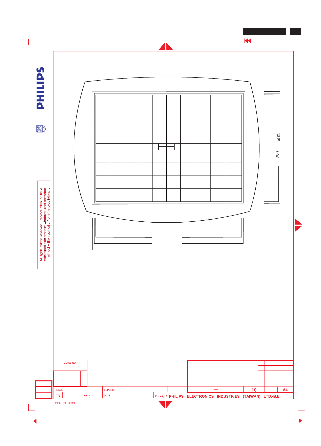
GENERAL PRODUCT SPECIFICATION
201P GS3 CM25
Go to cover page
73
1999-12-10
R.Y. CHOU
388
392
396
FIG-1 IMAGE DIMENSION
21”AUTO SCAN CMTR-CM25+ 201P
TYPE : 201P 10/00
BRAND : PHI
LIPS
99-12-10
mm
mm
mm
32
8639 000 10329
590
24
Back
Forward
Page 76
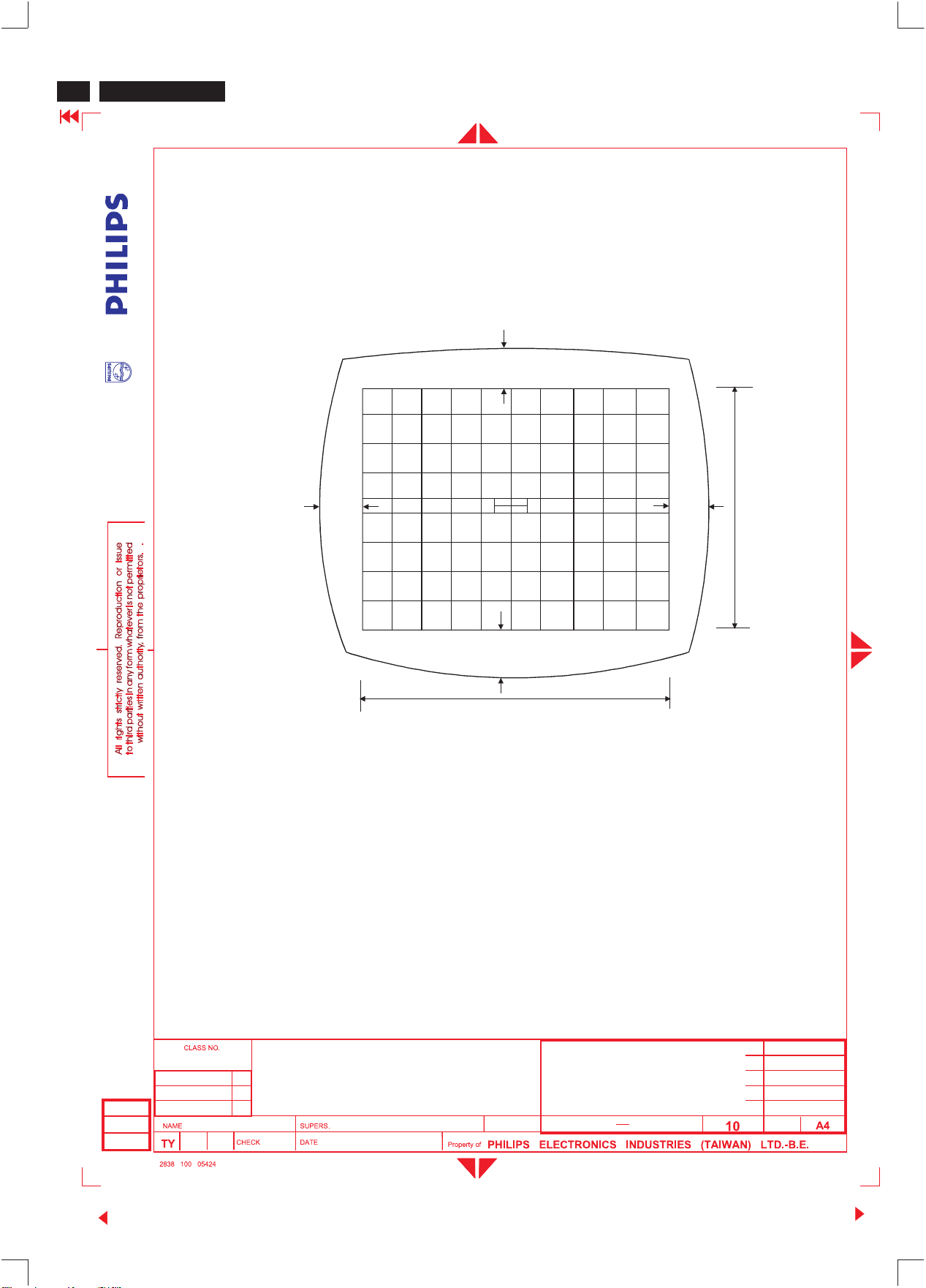
74
201P GS3 CM25
Go to cover page
GENERAL PRODUCT SPECIFICATION
C
A
B
mm
294
D
mm
392
|A-B| AND |C-D|<6mm
FIG-2 IMAGE CENTERING
Back
1999-12-10
R.Y. CHOU
21”AUTO SCAN CMTR-CM25+ 201P
TYPE : 201P 10/00
BRAND : PHI
LIPS
99-12-10
32
8639 000 10329
590
25
Forward
Page 77
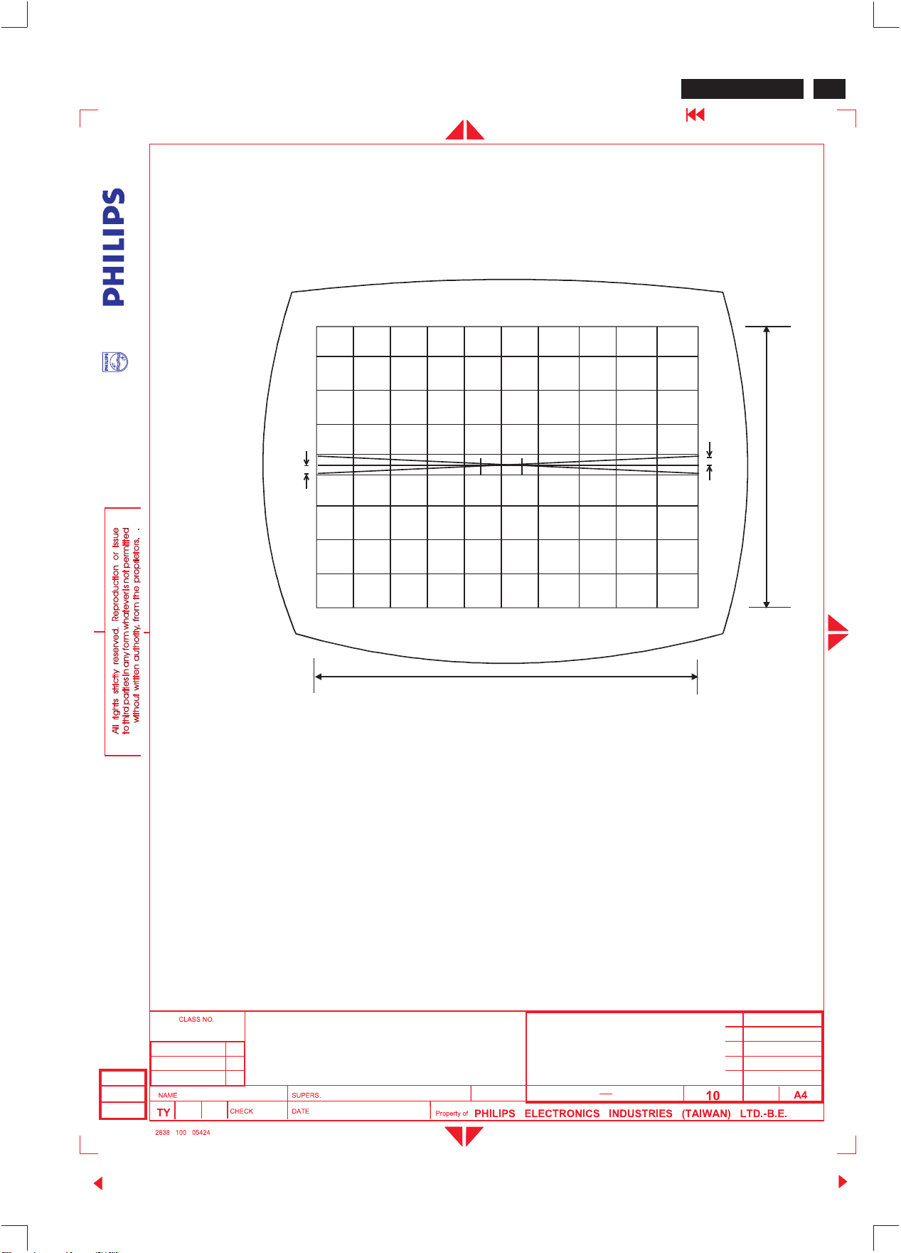
GENERAL PRODUCT SPECIFICATION
1
mm
201P GS3 CM25
Go to cover page
mm
1
75
mm
294
1999-12-10
R.Y. CHOU
FIG-3 IMAGE ROTATION
21”AUTO SCAN CMTR-CM25+ 201P
TYPE : 201P 10/00
BRAND : PHI
LIPS
99-12-10
32
mm
392
8639 000 10329
590
26
Back
Forward
Page 78
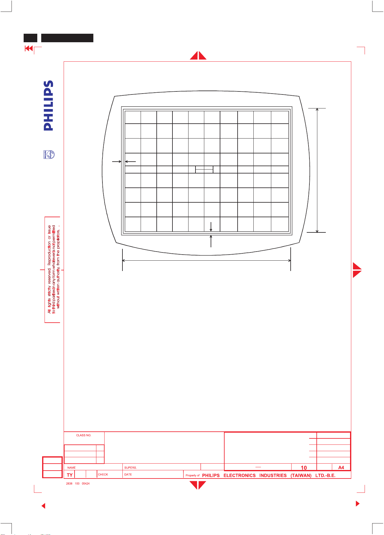
76
201P GS3 CM25
Go to cover page
GENERAL PRODUCT SPECIFICATION
mm
294
A
B
mm
392
A=B=2.5mm
FIG-4 IMAGE GEOMETRY
Back
1999-12-10
R.Y. CHOU
21”AUTO SCAN CMTR-CM25+ 201P
TYPE : 201P 10/00
BRAND : PHI
LIPS
99-12-10
32
8639 000 10329
590
27
Forward
Page 79
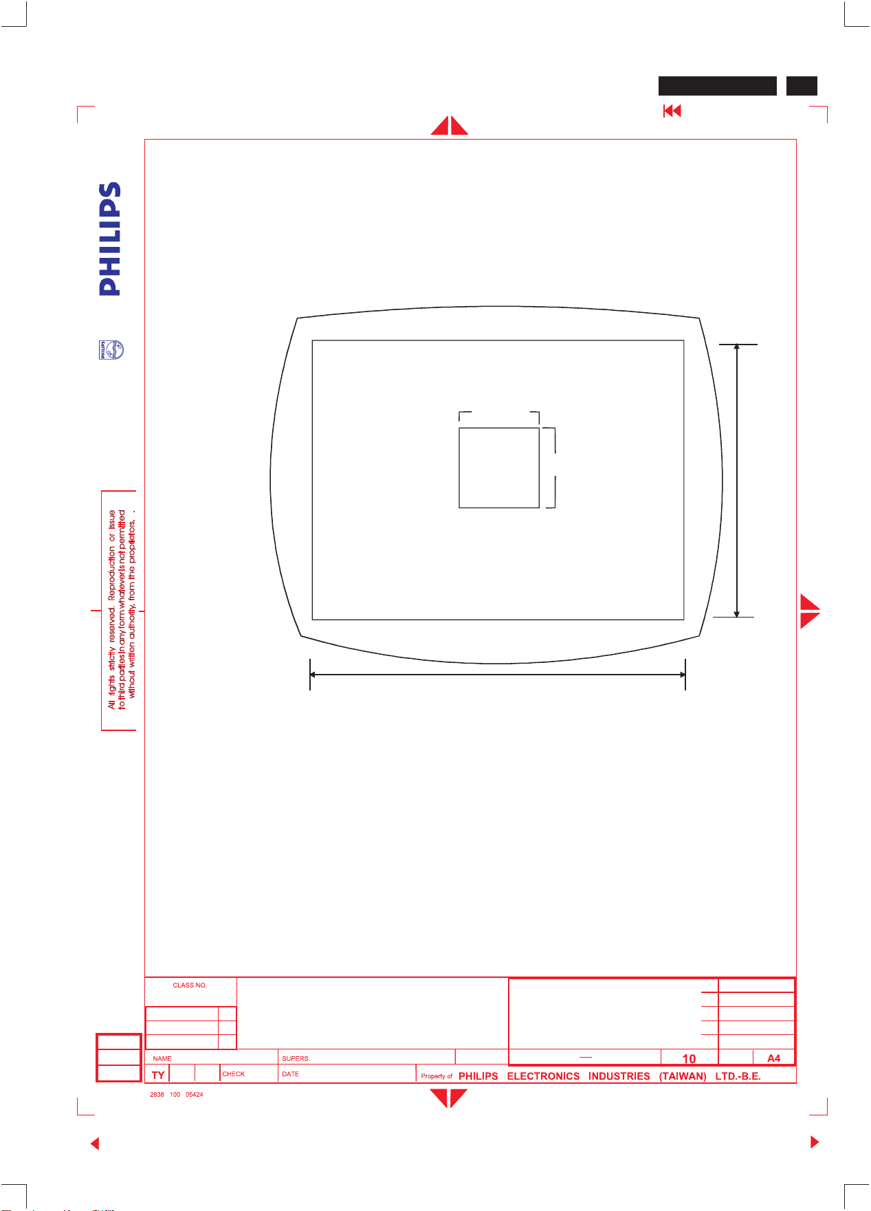
GENERAL PRODUCT SPECIFICATION
100
mm
ZONE-B
100
mm
201P GS3 CM25
Go to cover page
77
mm
294
ZONE-A
mm
392
FIG-5 BRIGHTNESS AND CONTRAST
MEASUREMENT AREA
Back
1999-12-10
R.Y. CHOU
21”AUTO SCAN CMTR-CM25+ 201P
TYPE : 201P 10/00
BRAND : PHI
LIPS
99-12-10
32
8639 000 10329
590
28
Forward
Page 80
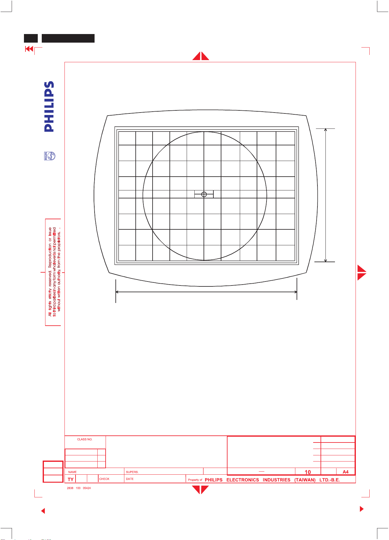
78
201P GS3 CM25
Go to cover page
GENERAL PRODUCT SPECIFICATION
ZONE B
ZONE A
ZONE C
mm
294
1999-12-10
R.Y. CHOU
FIG-6 MISCONVERGENCE
21”AUTO SCAN CMTR-CM25+ 201P
TYPE : 201P 10/00
BRAND : PHI
LIPS
99-12-10
392
32
B
mm
8639 000 10329
590
29
Back
Forward
Page 81
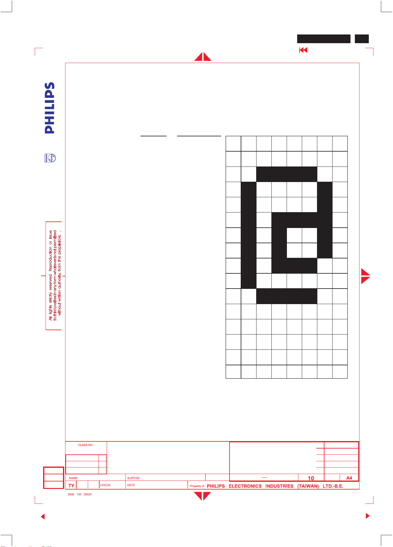
GENERAL PRODUCT SPECIFICATION
1BYTE=8BITS
201P GS3 CM25
Go to cover page
79
LINE
0
1
2
3
4
6
7
8
9
A
HEX.DATA
0000
0
00
3
4
4
55
5
5
5
4
3
C
2
2
E
2
2
C
0
C
6
7
54
3
1
2
0
1999-12-10
R.Y. CHOU
B
C
0
00
D
E
0
F
Fig 7 CHARACTER FORMAT FOR FOCUS CHECK
21”AUTO SCAN CMTR-CM25+ 201P
TYPE : 201P 10/00
BRAND : PHI
LIPS
99-12-10
0
00
0
00
8639 000 10329
32
590
30
Back
Forward
Page 82
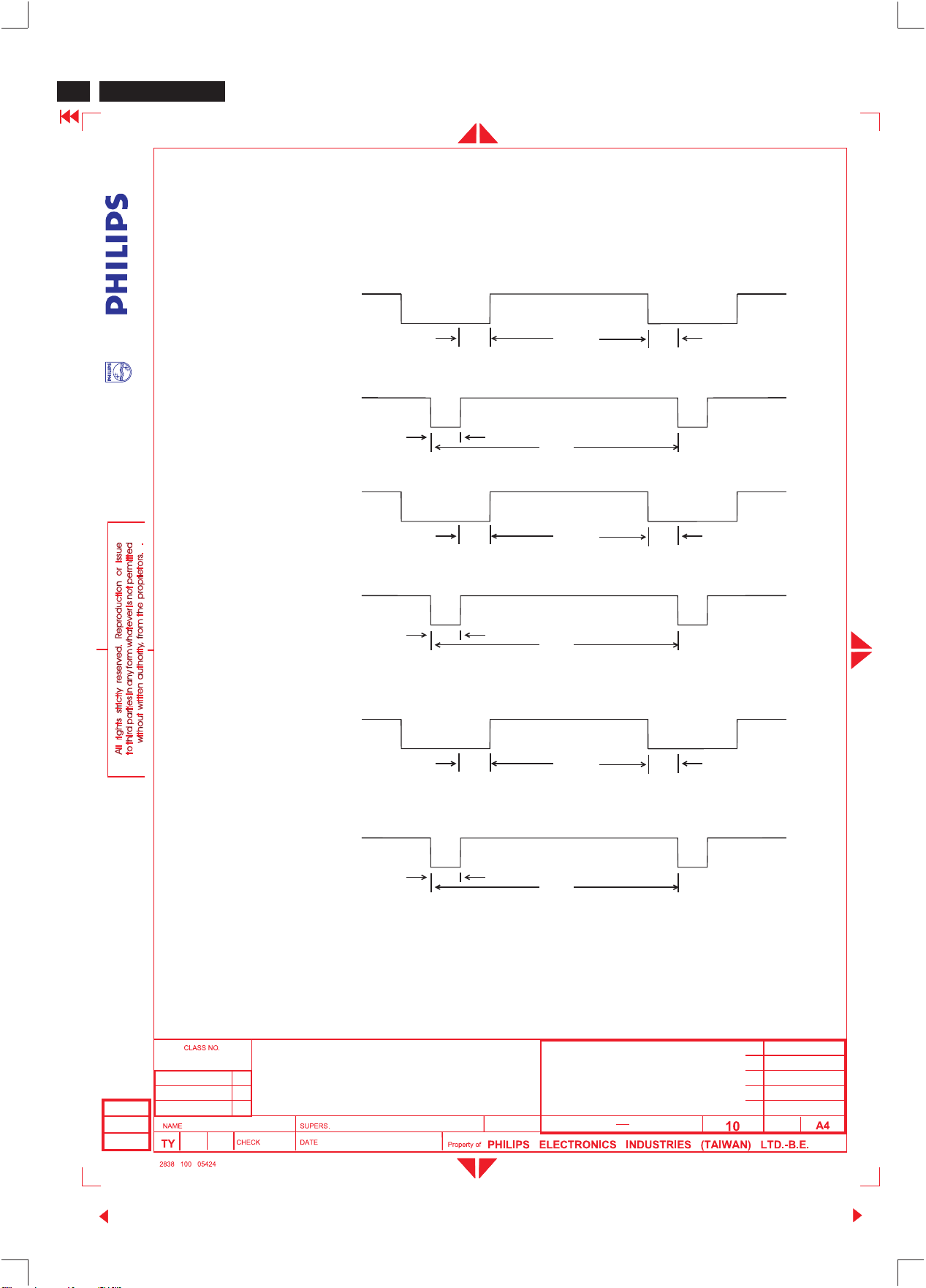
80
201P GS3 CM25
Go to cover page
GENERAL PRODUCT SPECIFICATION
SEPARATE SYNC.
VIDEO
HORIZONTAL
VERTICAL
COMPOSITE SYNC.
C
B
Q
P
D
A
VIDEO
R
O
VIDEO
E
S
1999-12-10
R.Y. CHOU
HORIZONTAL
B
FIG-8 TIMING CHART -1
21”AUTO SCAN CMTR-CM25+ 201P
TYPE : 201P 10/00
BRAND : PHI
LIPS
99-12-10
C
D
A
E
8639 000 10329
32
590
31
Back
Forward
Page 83
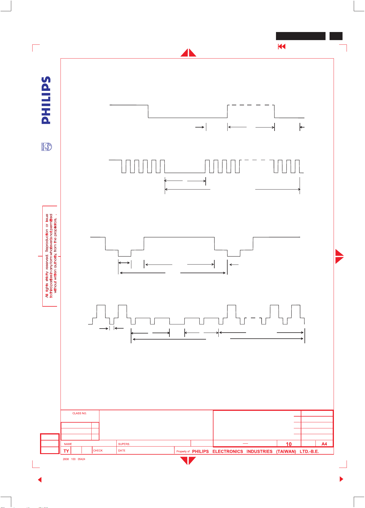
GENERAL PRODUCT SPECIFICATION
VIDEO
201P GS3 CM25
Go to cover page
81
VERTICAL
COMPOSITE SYNC.
( SYNC. ON GREEN )
HORIZONTAL
B
& VIDEO
C
QR S
P
O
D
A
E
1999-12-10
R.Y. CHOU
VERTICAL
21”AUTO SCAN CMTR-CM25+ 201P
TYPE : 201P 10/00
BRAND : PHI
B
S
P
Q
FIG-9 TIMING CHART -2
LIPS
32
99-12-10
O
8639 000 10329
590
R
32
Back
Forward
Page 84
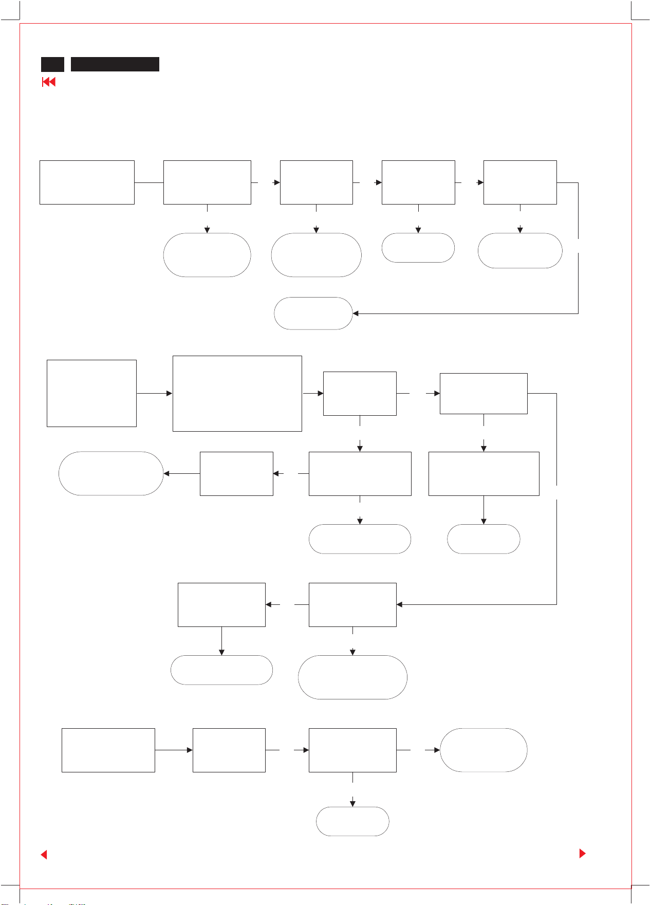
82
201P GS3 CM25
Go to cover page
A. Power Supply Failure
Repair Flow Chart
1. Sympton :
no startup sound
LED light off
2. Sympton :
hicup mode with
startup sound or
blinking LED
check
7141/7155/7144/7151
check 7121 pin1
Waveform right?
NO
check
1103/6101/
7121 pin3/2103
Turn power off
check the resistance for
all output voltages+210,
80,+15,-15,+6.3,+5V,check
6131,6133,6134,6137,6139
check 6161
Ok
check 7121
pin2
NO
check
3121/3123
replace 7121
check 7121
pin 4
No
check 6125
No
Ok
Ok
check 7121
pin 3
NO
replace 7121
OK
check 3121,3123,3125
Ok
check 7121
pin 1
No
check 7121
pin4
Ok
check
6111/3106/
3111/7111
NO
OK
3. Sympton:
abnormal sound
check 7143 pin3
voltage dip
check
+5V loading current
check
frequency
Ok
Ok
replace 5130
check 7143 pin1
12V< pin1 < 15V
No
check
6152/3151/3153
7151/2142
check 7121
drain waveform
right?
Ok
replace 5130
No
replace 5130
check
6104/3104/3105
2103/2104/2121
Back
Forward
Page 85
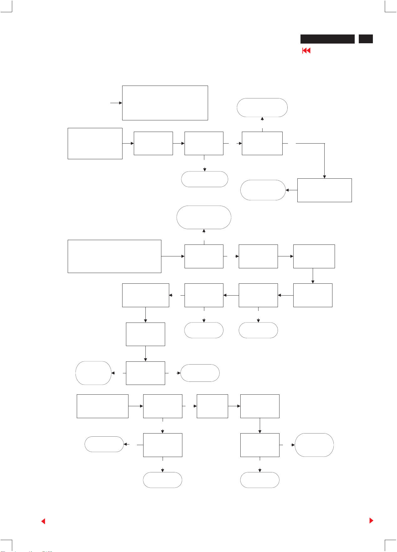
B.Video
Repair Flow
1.Sympton :
(with white pattern)
no picture
green LED on
Repair Flow Chart
rough check for R, G, B
1. video input~ 0.7V
2. 7704video output ~2.5V
3. 7711 video output~ 35V swing
check heater
= 6.3V
check
EHT~25KV
check Xray prot.
7651 pin14
check blanking
7421 pin16
No
check blanking
Ok
7421 pin16
Ok
check
VG1 < -190V
check
VG2 > 350V
201P GS3 CM25
Go to cover page
No
check DC restoration
7739,7769,7719
7740,7770,7720
83
2.Sympton :
no video (or dim),
only raster with/without retrace line
green LED on
check 7704 pin15
2V< ABL < 5V
check 7704
Pin27 HFLB
check
7421 pin16
3. Sympton :
no OSD or
OSD out of sync.
check 7704
pin19 CLBL
pin13,9,4 input
OkNo
check 7704
Ok
replace 7704
No
Ok
check Vg1
Vg1=0V
check 7704
pin 6,2,11
input swing
No
Replace
7704
check
7855 pin10
VFLB
No turn down Vg2
check 7711
Pin 2,6,10
input swing
No
replace 7711
Check 7855
pin2 VCO
pin3 RP
check cathode
+80V/+180V
check 7711
pin 4,8,12
Output swing
Back
check
7855 pin12
Ok
Ok
check
7704 pin1
No
replace 7704
check 7855
pin5 HFLB
No
replace 7855
Ok
check 7855
pin 7,8(IIC)
Forward
Page 86
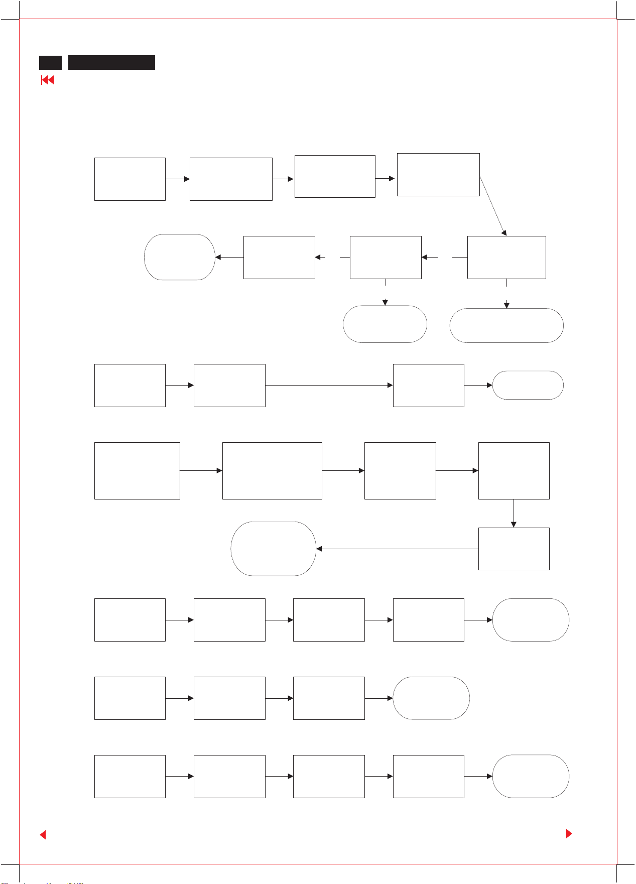
201P GS3 CM25
84
Go to cover page
C. Horizontal deflection
output repair flow :
Repair Flow Chart
1. Sympton :
without
H-deflection.
2. Sympton :
East /West
corr.
check B+ Control
7422,7423 base
replace 5543
check 2443
parabola
exist
check
210V
check B+ Control
7541 base
check Hsync
Ok
7541 drain
6604,5542,3546
check B+ Control
7421 base
No
check
check 7421
parabola exist
pin11
check B+ Control
Ok
7421 pin6
No
refer 7421 check list
or replace 7421
refer 7421
check list
3. Sympton :
H-linearity /H-DC
(full freq. range)
4. Sympton :
rotation
5. Sympton :
H_dc shift
enter factory mode
check linearity data
in eeprom
refer cpu
chece list
check cpu
pin 19~25
check
7502
check
7542,7543
check 7586
pin 1,4,8
check
7545 collector
7544 emitter
check
3528/7503
7504 emitter
check
3590/7587
/7588
check cpu
7301 pin28
control range
check 7505
pin 2,3,8
replace 3523
check cpu
7301 pin4
control range
Back
6. Sympton :
Focus
enter OSD
function
disable morier
check
7601collector
check
7421 pin 32
check
3617/5672/5601
Forward
Page 87
Repair Flow Chart
201P GS3 CM25
Go to cover page
85
D. Vertical Deflection Failure
Sympton :
one horizontal line
V_size is abnormal
too large/small (small)
basic check
+15/-15V
check
3578,3580
good
No
replace
3578,3580,7567
Ok
check
3571,3572
check
+15V,3569,6567
good?
No
replace
3569,6567,7567
Ok
Ok
check 7567
pin2,pin3 ramp
exist ?
No
check
7421
Back
Forward
Page 88
201P GS3 CM25
86
Go to cover page
Repair Flow Chart
E. CPU
check list
Basic Check
1. H-linearity
2. H-Centering
3. Blank
Pin20~25 (S6~S1)
S-cap switch
7. ABL-Adj
check cpu pin11/pin32=5V
pin9/pin10=12MhZ
pin12/pin31=gnd
check pin42
pwm from 0V to 5V
check pin28
pwm from 0V to 5V
check pin2
normal : low
change timing : Hi
check Q1~Q6
Pin20~25
low:0
hi :1
check pin29
pwm from 0V to 5V
Hor. Freq.(KHz)
~33.00
33.00~36.00
36.00~42.00
42.00~45.00
45.00~47.50
47.50~49.00
49.00~52.00
52.00~55.00
55.00~58.50
58.50~61.50
61.50~65.00
65.00~70.00
70.00~73.00
73.00~76.00
76.00~82.50
82.50~88.50
88.50~98.00
98.00~102.00
102.00~110.00
110.00~
Q6 Q5 Q4 Q3 Q2 Q1
111111
011101
011001
001110
111010
011010
011010
100010
111100
110100
010100
000100
111000
011000
101000
001000
110000
010000
100000
000000
Back
13,14,16,17
Hsync/Vsync
18. Hunlock
6.7 P.S.
LED
check sync.
hin=pin13
vin=pin16
hout=pin14
vout=pin17
check pin18
normal=Hi
blank=low
check pin6/7
1. Normal
Fvout=Fvin
2. sync out of rang
Fhin>121KHz
Fvin>160Hz
pin7 pin6
normal hi hi
standby hi low
suspend low hi
off low low
Forward
Page 89
1. Degauss
Repair Flow Chart
check
active=hi
no active=low
201P GS3 CM25
Go to cover page
87
26, Reset
30. Brightness
4. Rotation
33. Keypad
Selftest
check
from 5V to 0V
check
pwm from 0V to 5V
check
pwm from 0V to 5V
check keys
ok,up,down,left,right
check pin34
1.no H/V sync & first power ON - show msg.
2.H/V sync exist - normal
3.H/V sync non-exist & after power ON - power saving
4.Left+Right Keys pressed with IFcable - factory mode
5.left +Right Keys pressed without IF cable - burn in mode
check
2317/6301
6302/3322
check 3319,
3891~3895
36,37. DDC bus
38,39. IIC bus
40,41. EEPROM
write protection
35. USB int
check idle status
sda=pin36=hi
scl=pin37=hi
check idle status
sda=pin38=hi
scl=pin39=hi
check pin40 pin41
write : low low
read : don't care
normal : hi hi
pin35
hi : active
low : no active
check
7336 M24C16
7421 TDA4856
7781 LSC4389
7701 TDA4886A
Back
Forward
Page 90
88
201P GS3 C 25
Go to cover page
M
Repair Flow Chart
F. TDA4856
Check List
1. HFLB
(from H.defl)
3.4.5.6 B+ control
8. HDRV
Basic check
Vcc>9V
during startup
if no exist
a pin3 amplify pin5 and it compare to pin4
b. pin4 generate the saw_tooth wave
c. pin5 input voltage for the square output waveform
d. pin6 pwm output to 7422 & 7423 base
to H_deflection.
7425&7426 base
Vcc=pin10=12V
gnd =pin7=pin25=0v
pin16
CLBL=hi
inhibit pin6 output
if pin3 is pulled to
ground by 7508
11.EWDRV
12,13 Vout1/Vout2
14,15
Vsync,Hsync
16. CLBL
to B+ control
east/west control
differential input
to 7567 pin 1, 7
the input sync from
7404 pin 14,15
Vertical blank will be activated = hi
1.pin30 = softstart pll2 = 0V
2.pin26 = pll1 is unlock in searching mode
3.pin1 = HFLB no exist
4.pin10 = Vcc < 9V
Back
Forward
Page 91
Repair Flow Chart
201P GS3 CM25
Go to cover page
89
17. Hunlock
18. IIC SCL = hi
19 IIC SDA = hi
20 asymmetry EW
output
21 EHT_compen.
Hunlock pin is floating while pll1(pin26) is
unlock in searching mode
initial fail could be these of IC
7421,7701,7781,7336
to 7503 pin30
for soft start
compensate for the V_size
owing the load variation
22,23,24
VAGC,VREF,VCAP
26,27,28,29
Hpll1,Hbuf,Href, Hcap
30. PLL2
pin22 determin the AGC
pin23,pin24 determin frequency
pin26 determin the
pll1 loop filter
pin 27,28,29 H-Freq
working range
1.compare the HFLBand control the phase of HDRV
2.softstart
compensate for the H_size owing the load variation31 EHT_compen.
30K<freq.<121KHz
50Hz< freq. <160Hz
32. Focus to 7603 for the V dynamic focus
Back
Forward
 Loading...