

Philips 1N4532, 1N4531 Datasheet
DISCRETE SEMICONDUCTORS
DATA SH EET
ook, halfpage
M3D050
1N4531; 1N4532
High-speed diodes
Product specification
Supersedes data of April 1996
1996 Sep 03
Philips Semiconductors Product specification
High-speed diodes 1N4531; 1N4532
FEATURES
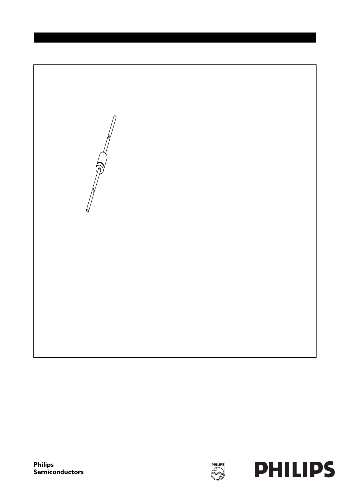
• Hermetically sealed leaded glass
SOD68 (DO-34) package
• High switching speed: max. 4 ns
DESCRIPTION
The 1N4531, 1N4532 are high-speed switching diodes fabricated in planar
technology, and encapsulated in hermetically sealed leaded glass
SOD68 (DO-34) packages.
• Continuous reverse voltage:
max. 75 V
• Repetitive peak reverse voltage:
max. 75 V
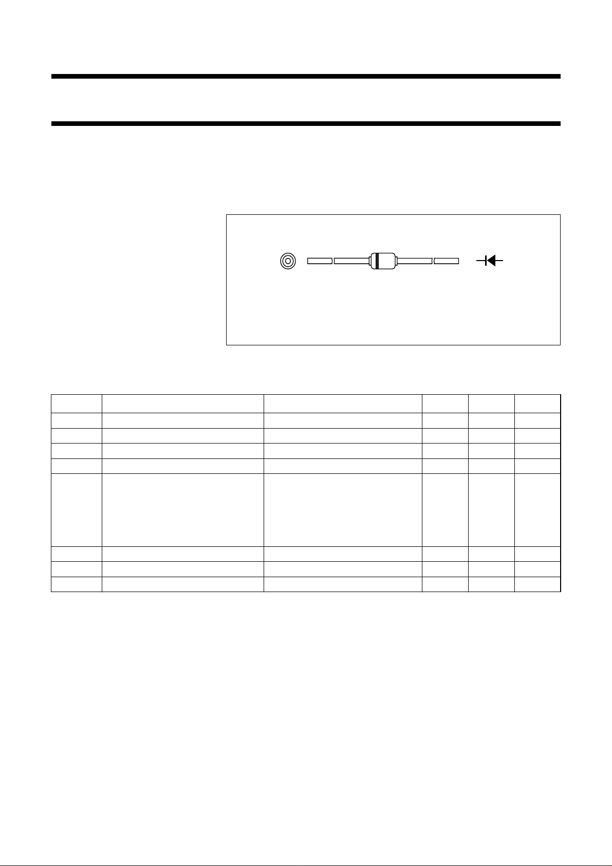
handbook, halfpage
k
a
• Repetitive peak forward current:
max. 450 mA.
APPLICATIONS
• High-speed switching
The diodes are type branded.
Fig.1 Simplified outline (SOD68; DO-34) and symbol.
MAM156
• Protection diodes in reed relays.
LIMITING VALUES
In accordance with the Absolute Maximum Rating System (IEC 134).
SYMBOL PARAMETER CONDITIONS MIN. MAX. UNIT
V
V
I
F
I
FRM
I
FSM
RRM
R
repetitive peak reverse voltage − 75 V
continuous reverse voltage − 75 V
continuous forward current see Fig.2 − 200 mA
repetitive peak forward current − 450 mA
non-repetitive peak forward current square wave; Tj=25°C prior to
surge; see Fig.4
t=1µs − 4A
t=1ms − 1A
t=1s − 0.5 A
P
tot
T
stg
T
j
total power dissipation T
=25°C − 500 mW
amb
storage temperature −65 +200 °C
junction temperature − 200 °C
1996 Sep 03 2

Philips Semiconductors Product specification
High-speed diodes 1N4531; 1N4532
ELECTRICAL CHARACTERISTICS
T
=25°C; unless otherwise specified.
j
SYMBOL PARAMETER CONDITIONS MIN. MAX. UNIT
V
F
I
R
C
d
t
rr
V
fr
forward voltage IF= 10 mA; see Fig.3 − 1000 mV
reverse current see Fig.5
IN4531 V
IN4532 V
=20V − 25 nA
R
=20V; Tj= 150 °C − 50 µA
V
R
=50V − 100 nA
R
V
=50V; Tj= 150 °C − 100 µA
R
diode capacitance f = 1 MHz; VR= 0; see Fig.6
IN4531 − 4pF
IN4532 − 2pF
reverse recovery time when switched from IF= 10 mA to
IN4531 − 4ns
IN4532 − 2ns
reverse recovery time when switched from I
IN4532 − 4ns
IR= 60 mA; RL= 100 Ω;
measured at IR= 1 mA; see Fig.7
= 10 mA to
F
IR= 10 mA; RL= 100 Ω;
measured at IR= 1 mA; see Fig.7
forward recovery voltage when switched from IF= 100 mA;
− 3V
tr≤ 30 ns; see Fig.8
THERMAL CHARACTERISTICS
SYMBOL PARAMETER CONDITIONS VALUE UNIT
R
R
th j-tp
th j-a
thermal resistance from junction to tie-point lead length 5 mm 120 K/W
thermal resistance from junction to ambient lead length 5 mm; note 1 350 K/W
Note
1. Device mounted on a printed circuit-board without metallization pad.
1996 Sep 03 3
 Loading...