

Philips 191E2SB/27, 191E2SB/75, 191E2SB/71, 191E2SB/00, 191E2SB/73 Service Manual
...
18.5ƎLCD Color Monitor Chassis: Meridian 2
Service
Service
Service
Description
Page
Table of Contents.........................................………….1
Revision List.............................................…………….2
Important Safety Notice…………................................3
1. Monitor Specifications….........................................4
2. LCD Monitor Description….....................................7
3. Operation Instructions….......................................9
3.1General Instructions………………………….…...9
3.2 Control Buttons…………..……….…………….…9
3.3 OSD Menu………………….................................10
4. Input/output Specification..........................……….11
4.1 Input Signal Connector.............................………11
4.2 Resolution & Preset Modes.................................12
4.3 Pixel Defect Policy…………………………………13
4. 4 Failure Mode of Panel……………………………15
5. Block Diagram…………………………................16
5.1 Scaler Board....................................………….....16
5.2 Power Board........…………………………...........18
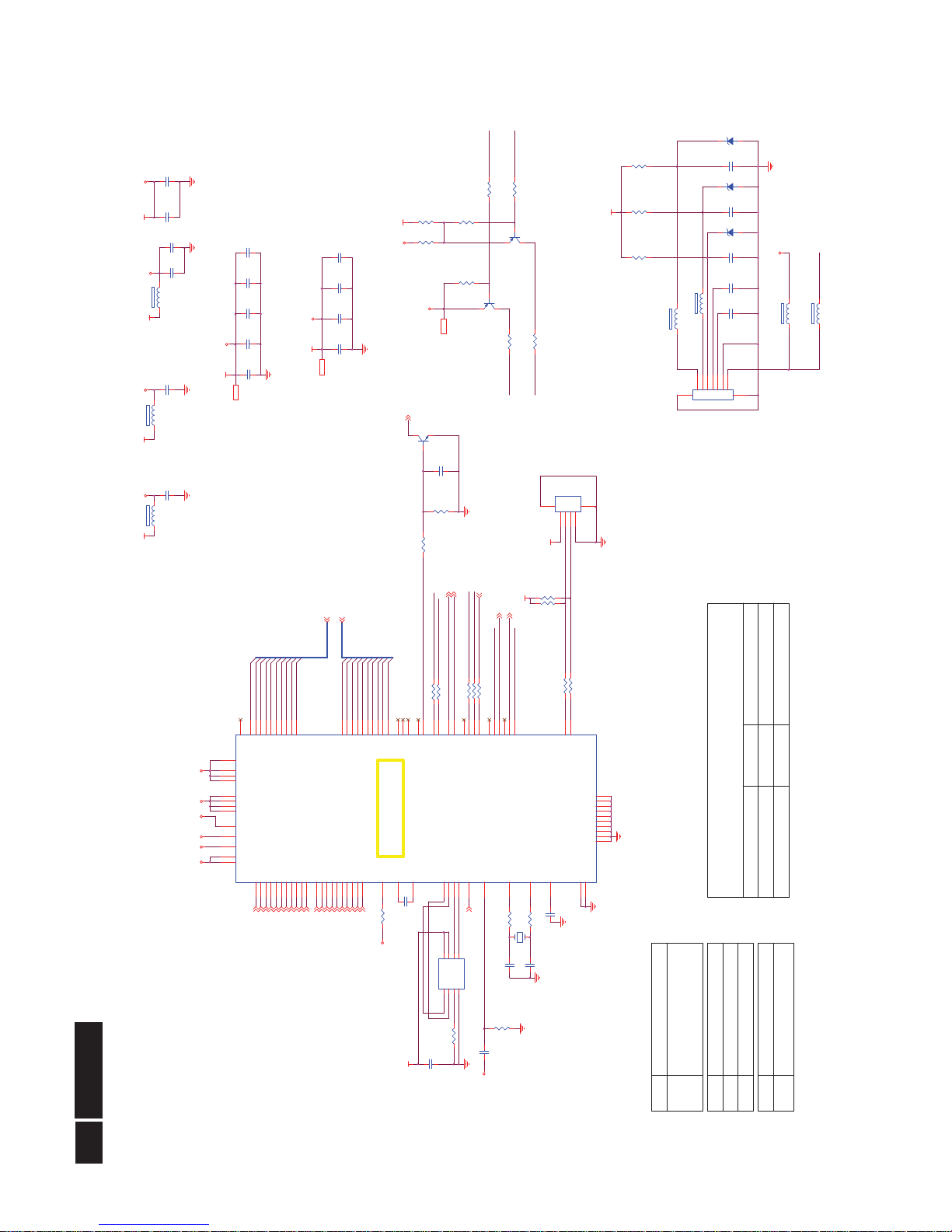
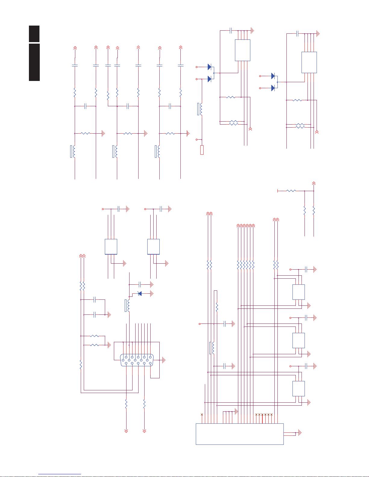
6. Schematic Diagram.............................................. 19
6.1 Scaler Board…………………….…………………28
6.2 Adapter Board..............................................…...28
Description
Page
6.3 Inverter Board...............................................…...29
6.4 Converter Board...........................................…...30
6.5 Key Board…….……………………………………33
7. PCB Layout………………………………………...34
7.1 Scaler Board……………………………………..34
7.2 Adapter Board……………...………………………36
7.3 Inverter Board……….……………………………37
7.4 Converter Board…………………………………38
7.5 Key Board………...………………………………41
8. Wiring Diagram………………………………….…..42
9. Scaler Board Overview…………………………....43
10. Mechanical Instructions………………………....44
1 1. Repair Flow Chart…….……………………………47
12. ISP Instructions...…............................................51
13. DDC Instructions….............................................58
14. White Balance, Luminance Adjustment…...........71
15. Monitor Exploded View…....................................73
16. Recommended & Spare Parts List...….............74
17. Different Parts List……………………….……….88
18. General Product Specification………….……….93
SAFETY NOTICE
ANY PERSON ATTEMPTING TO SERVICE THIS CHASSIS MUST FAMILIARIZE HIMSELF WITH THE
CHASSIS AND BE AWARE OF THE NECESSARY SAFETY PRECAUTIONS TO BE USED WHE N
SERVICING ELECTRONIC EQUIPMENT CONTAINING HIGH VOLTAGES.
CAUTION: USE A SEPARATE ISOLATION TRANSFOMER FOR THIS UNIT WHEN SERVICING
REFER TO BACK COVER FOR IMPORTANT SAFETY GUIDELINES
Copyright 2010 Philips Consumer Lifestyle Subject to modification ƻK Mar.31, 2010
191E2SB/00
191E2SB/10
191E2SB/27
191E2SB/62
191E2SB/69
191E2SB/71
191E2SB/73
191E2SB/75
191E2SB/93
191E2SB/94
191EL2SB/00
191EL2SB/10
191EL2SB/27
191EL2SB/69
191EL2SB/71
191EL2SB/75
191EL2SB/78
191EL2SB/93
191EL2SB/94
191EL2SB/96
191EL2SB/67
191EL2SB/70
191EL2SB/55
191EL2SB/01

!
!
Meridian 2
2
Revision List
Version Release Date Revision History
A00 Mar.31,2010 Initial release, Draft Version
A01 May.04,2010
Update BOM for 191EL2SB/00 and 191E2SB/69
Update Monitor Specifications, Operating Instructions and Resolution & Preset
Modes
A02 May.22,2010 Add AUO panel for 191EL2SB/69 and update BOM for 191EL2SB/96
A03 Jun.26,2010
Add CTN model 191EL2SB/71
Add CPT and TPV panel for 191EL2SB/00
Update BOM for 191E2SB/00, 191EL2SB/75 and 191EL2SB/93
A04 Aug.16,2010
Update BOM for 191E2SB/62
Add CTN model 191EL2SB/78
Add CPT and TPV panel for 191EL2SB/71
Update BOM of TPV panel for 191EL2SB/00, 191EL2SB/69
A05 Sep.19,2010
Update BOM for 191EL2SB/00, 191EL2SB/69, 191EL2SB/71, 191EL2SB/75
and 191EL2SB/96
A06 Oct.19,2010
Add CTN models 191EL2SB/67 and 191EL2SB/70
Add AUO VD p anel for 191EL2SB/75
A07 Dec.20,2010
Add AUO VD panel for 191EL2SB /00, 191EL2SB/69, 191EL2SB/70,
191EL2SB/71, 191EL2SB/93, 191EL2SB/94 and 191EL2SB/96 (1A+1D)
Lead into the new coverter board (pcb:715G4137P01000004S) for AUO panel
A08 Apr.18,2011 Add TPV panel for 191EL2SB/93
A09 May.12,2011
Add Auto Color SOP into ISP Instructions
Update BOM for 191E2SB/62 and add CPT panel for 191EL2SB/94
A10 Jul.07,2011 Add CTN model 191EL2SB/55
A11 Sep.22,2011
Add CTN model 191EL2SB/01
Update BOM for 191EL2 all models
Lead into the new scaler board (pcb: 715G4411M01000004I) and converter
board (pcb: 715G4704P01001004I) for AUO VDT0, SEC and CPT0 panel

3
Meridian 2
Important Safety Notice
Proper service and repair is important to the safe, reliable operation of all Philips Company Equipment. The servi ce
procedures recommended by Philips and described in this service manual are effective methods of performing
service operations. Some of these service operations require the use of tools specially designed for the purpose.
The special tools should be used when and as recommended.
It is important to note that this manual contains various CAUTIONS and NOTICES which should be carefully read
in order to minimize the risk of personal injury to service personnel. The possibility exists that improper service
methods may damage the equipment. It is also important to understand that these CAUTIONS and NOTICE S ARE
NOT EXHAUSTIVE. Philips could not possibly know , evaluate and advise the service trade of all conceivable ways
in which service might be done or of the possible hazardous consequences of each way. Consequently, Philips has
not undertaken any such broad evaluation. Accordingly, a customer who uses a service procedure or tool which is
not recommended by Philips must first satisfy himself thoroughly that neither his safety nor the safe operation of
the equipment will be jeopardized by the service method selected.
Hereafter throughout this manual, Philips Company will be referred to as Philips.
WARNING
Use of substitute replacement parts, which do not have the same, specified safety characteristics, may create
shock, fire, or other hazards.
Under no circumstances should the original design be modified or altered without written permission from Philips.
Philips assumes no liability, express or implied, arising out of any unauthorized modification of design.
FOR PRODUCTS CONTAINING LASER:
DANGER- There is invisible laser radiation when open. AVOID DIRECT EXPOSURE TO BEAM.
CAUTION-Use of controls or adjustments or performance of procedures other than those specified herein may
result in hazardous radiation exposure.
CAUTION -The use of optical instruments with this product will increase eye hazard.
TO ENSURE THE CONTINUED RELIABILITY OF THIS PRODUCT, USE ONLY ORIGINAL MANUFACTURER'S
REPLACEMENT PARTS, WHICH A RE LISTED WITH THEIR PART NUMBERS IN THE PARTS LIST SECTION
OF THIS SERVICE MANUAL.
Take care during handling the LCD module with backlight unit:
-Must mount the module using mounting holes arranged in four corners.
-Do not press on the panel, edge of the frame strongly or electric shock as this will result in damage to the screen.
-Do not scratch or press on the panel with any sharp objects, such as pen cil or pen as this ma y result in damage to
the panel.
-Protect the module from the ESD as it may damage the electronic circuit (C-MOS).
-Make certain that treatment person’s body is ground ed through wristband.
-Do not leave the module in high temperature and in areas of high humidity for a long time.
-Avoid contact with water as it may a short circuit within the module.
-If the surface of panel becomes dirty, please wipe it off with a soft material. (Cleaning with a dirty or rough cloth
may damage the panel.)
!
!
Meridian 2
4
1. Monitor Specifications
Technical specifications
Picture/Display
LCD Panel Type TFT-LCD
Backlight CCFL (191E2) / LED (191EL2)
Panel Size 18.5Ǝ W (47cm)
Aspect Ratio 16:9
Pixel Pitch 0.300 x 0.300 mm
Brightness 250 cd/m²
SmartContrast 500,000:1 (191E2) / 20,000,000:1 (191EL2)
Contrast Ratio (typ.) 1000:1
Response Time (typ.) 5 ms
Optimum Resolution 1366 x 768 @ 60Hz
Viewing Angle 176° (H) / 170° (V) @ C/R>5
Picture Enhancement SmartImage Lite
Display Colors 16.7 M
Vertical Refresh Rate 56Hz - 76Hz
Horizontal Frequency 30kHz - 83kHz
sRGB YES
Connectivity
Signal Input DVI-D (Digital, HDCP),VGA (Analog)
Input Signal Separate Sync, Sync on Green
Convenience
User Convenience SmartImage/ź ,Input/Ÿ, 4:3 Wide/Back, Menu (OK), Power On/Off
OSD Languages
English, French,
German
, Italian, Russian, Spanish, Simplified
Chinese, Portuguese
Other Convenience Kensington lock
Plug & Play Compatibility DDC/CI, sRGB, Windows 7/Vista/XP, Mac OSX, Linux
Stand
Tilt
-3 / +12 (191E2/191EL2)
Power (191E2)
On mode 21.4 W (typ.)
Energy Consumption
(EnergyStar 5.0 test method)
AC Input Voltage at
100VAC +/- 5VAC,
50Hz +/- 3Hz
AC Input Voltage at
115VAC +/- 5VAC,
60Hz +/- 3Hz
AC Input Voltage at
230VAC +/- 5VAC,
50Hz +/- 3Hz
Normal Operation (typ.) 16.33 W 16.32 W 16.30 W
Sleep 0.43 W 0.42 W 0.43 W
Off 0.42 W 0.42 W 0.43 W
5
Meridian 2
Heat Dissipation*
AC Input Voltage at
100VAC +/- 5VAC,
50Hz +/- 3Hz
AC Input Voltage at
115VAC +/- 5VAC,
60Hz +/- 3Hz
AC Input Voltage at
230VAC +/- 5VAC,
50Hz +/- 3Hz
Normal Operation 68.33 BTU/hr 68.29 BTU/hr 68.20 BTU/hr
Sleep 1.47 BTU/hr 1.43 BTU/hr 1.47 BTU/hr
Off 1.43 BTU/hr 1.43 BTU/hr 1.47 BTU/hr
Power (191EL2)
On mode 13.9W (typ.)
Energy Consumption
(EnergyStar 5.0 test method)
AC Input Voltage at
100VAC +/- 5VAC,
50Hz +/- 3Hz
AC Input Voltage at
115VAC +/- 5VAC,
60Hz +/- 3Hz
AC Input Voltage at
230VAC +/- 5VAC,
50Hz +/- 3Hz
Normal Operation (typ.) 10.49 W 10.50 W 10.44 W
Sleep 0.43 W 0.42 W 0.41 W
Off 0.42 W 0.42 W 0.40 W
Heat Dissipation* AC Input Voltage at
100VAC +/- 5VAC,
50Hz +/- 3Hz
AC Input Voltage at
115VAC +/- 5VAC,
60Hz +/- 3Hz
AC Input Voltage at
230VAC +/- 5VAC,
50Hz +/- 3Hz
Normal Operation 43.89 BTU/hr 43.93 BTU/hr 43.68 BTU/hr
Sleep 1.47 BTU/hr 1.43 BTU/hr 1.71 BTU/hr
Off 1.43 BTU/hr 1.43 BTU/hr 1.67 BTU/hr
Power LED indicator On mode: White, Standby/Sleep mode: White (blinking)
Power Supply AC Adapter, 1.2V==3.0A
Dimension
Product with Stand (W x H x D) 457 x 338 x 189 mm
Product without Stand (W x H x D) 457 x 293 x 41 mm
Box Dimension (W x H x D) 503 x 383 x 125 mm
Weight
Product with Stand 2.38 kg
Product without Stand 2.22 kg
Product with Packaging 3.58 kg
Operating Condition
Temperature Range (operation) 0°C to 40 °C
Temperature Range (storage) -20°C to 60°C
Relative Humidity 20% to 80%
Altitude
Non-operation: +12,000 ft (3,658 m)
Operation: + 40,000 ft (12,192 m)
MTBF 50,000 hrs (191E2) / 30,000hrs (191EL2)
!
!
Meridian 2
6
Environmental
ROHS YES
EPEAT Silver. (www.epeat.net)
Packaging 100% recyclable
Compliance and standards
Regulatory Approvals
CE Mark, FCC Class B, SEMKO, TÜV/GS, TÜV Ergo, UL/cUL,
Energy star 5.0
Cabinet
Color Black / Black
Finish Glossy / Texture
Note:
This data is subject to change without notice.
Go to www.philips.com/support
to download the latest version of leaflet.
7
Meridian 2
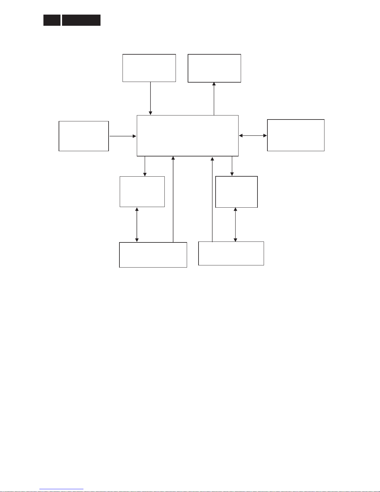
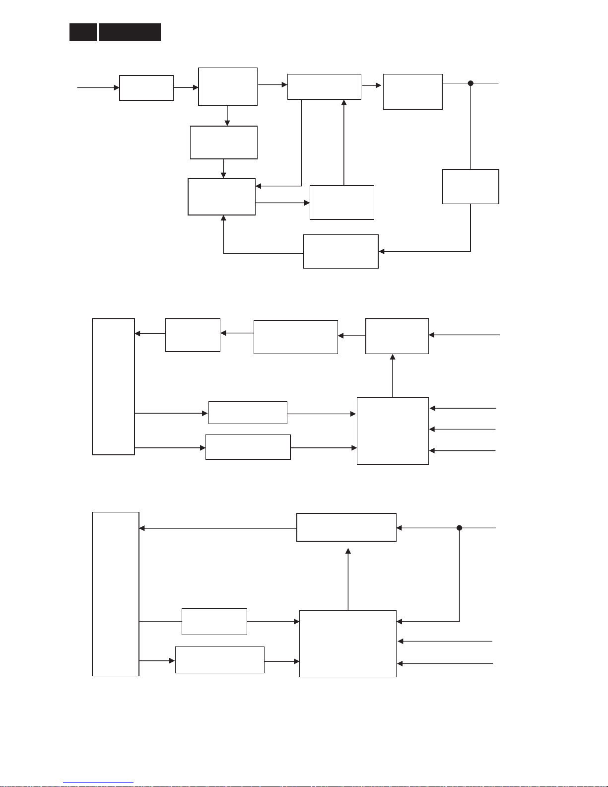
2. LCD Monitor Description
191E2
The LCD monitor will contain a scaler board, an adapter board, an inverter board and a key board. The scaler
board houses the flat panel control logic, brightness control logic and DDC.
The adapter board will provide AC to DC Inverter voltage to drive the backlight of panel and the scaler board chips
each voltage.
Monitor Block Diagram
DC 12V
Inverter Board
Flat Panel and
CCFL backlight
Scaler Board
DVI-D
D-SUB
CCFL Drive.
Key Board
Video signal, DDC
HOST Computer
Adapter Board
AC IN
90 ~ 264 V
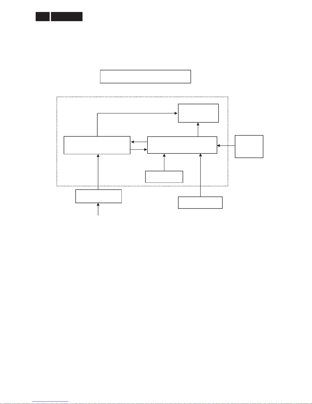
!
!
Meridian 2
8
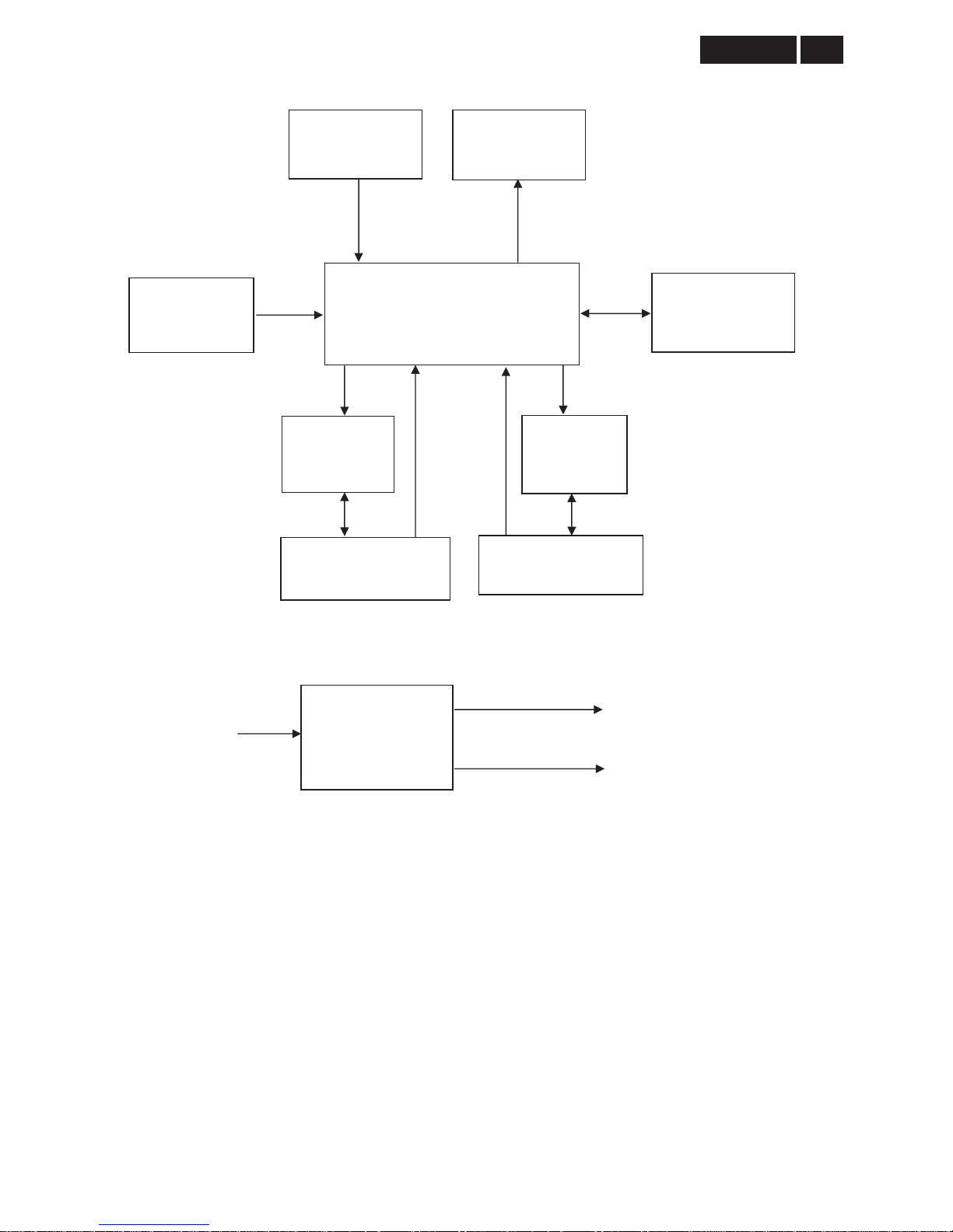
191EL2
The LCD monitor will contain a scaler board, an adapter board, a converter board and a key board. The scaler
board houses the flat panel control logic, brightness control logic and DDC.
The adapter board will provide AC to DC Inverter voltage to drive the backlight of panel and the scaler board chips
each voltage.
Monitor Block Diagram
DC 12V
Converter Board
LED Panel
Scaler Board
DVI-D
D-SUB
LED Drive
Video signal, DDC
Key Board
HOST Computer
Adapter Board
AC IN
90 ~ 264 V
9
Meridian 2
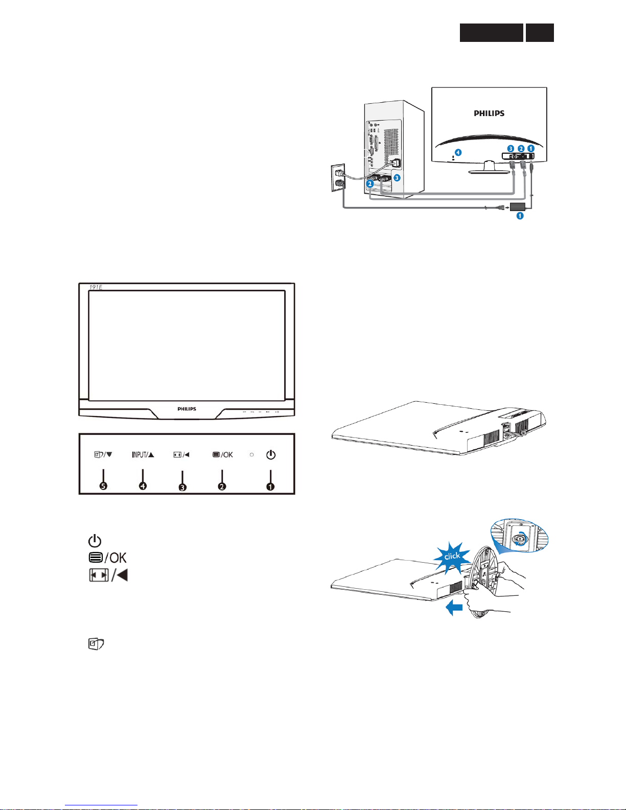
3. Operating Instructions
3.1 General Instructions
Press the power button to turn the monitor on or off.
The other control knobs are located at front panel of
the monitor (see figure). By changing these setting,
the picture can be adjusted to your personal
preference.
γ The power cord should be connected.
γ Press the power button to turn on the monitor. The
power indicator will light up.
3.2 Control Buttons
Operating the Monitor
Front view product description
1.
To switch monitor’s power ON and OFF.
2.
: To access the OSD menu
3.
: Change to 4:3 display. Return to
previous OSD level.
4. INPUT/Ÿ: To change the signal input source
and adjust the OSD menu.
5.
/: SmartImage Lite. There are three
modes to be selected: Standard, Internet, and
Game. To adjust the OSD menu
Connecting to your PC
1. DC power input
2. VGA input
3. DVI-D input (available for selected models)
4. Kensington anti-thief lock
Install base stand
1. Place the monitor face down a smooth
surface taking care to avoid scratching or
damaging the screen.
2. Attach the monitor base stand to the base
column then fasten base stand.

!
!
Meridian 2
10
3.3 OSD Menu
On-screen Display (OSD) is feature in all Philips LCD
monitors. It allows an end user to adjust screen
performance or select functions of the monitors directly
through an on-screen display inter face is shown as
below.
Basic and simple instruction on the control keys
In the OSD shown above users can press źŸ buttons
at the front bezel of the monitor to move the cursor, OK
to confirm the choice or change.
The OSD tree
Below is an overall view of the structure of the
On-Screen Display. You can use this as a reference
when you want to work your way around the different
adjustments later on.

11
Meridian 2
4. Input/ Output Specification
4.1 Input Signal Connector
Analog connectors
Pin No.
Signal Name
Pin No.
Signal Name
1
Red
9
DDC +3V or +5V
2
Green/SOG
10
Logic (GND)
3
Blue
11
Sense (GND)
4
Sense (GND)
12
Bi-directional Data
5
Cable Detect (GND)
13
H/H+V Sync
6
Red GND
14
V-sync
7
Green GND
15
Data Clock
8
Blue GND
Digital connectors (Option)
Pin No.
Signal Name
Pin No.
Signal Name
1
T.M.D.S. data2-
13
No Connect
2
T.M.D.S. data2+
14
+5V Power
3
T.M.D.S. data2 shield
15
Ground (for +5V) – Cable detect
4
No Connect
16
Hot plug detect
5
No Connect
17
T.M.D.S. data0-
6
DDC clock
18
T.M.D.S. data0+
7
DDC data
19
T.M.D.S. data0 shield
8
No Connect
20
No Connect
9
T.M.D.S. data1-
21
No Connect
10
T.M.D.S. data1+
22
T.M.D.S clock shield
11
T.M.D.S. data1 shield
23
T.M.D.S. clock+
12
No Connect
24
T.M.D.S. clock-
!
!
Meridian 2
12
4.2 Resolution & Preset Modes
Maximum Resolution
1366 x 768 at 60 Hz (analog input)
1366 x 768 at 60 Hz (digital input)
Recommended Resolution
1366 x 768 at 60 Hz (digital input)
H. freq (kHz) Resolution V. freq (Hz)
31.47 640 x 480 59.94
37.88 800 x 600 60.32
48.36 1024 x 768 60.00
54.00 1152 x 864 60.00
44.77 1280 x 720 59.86
47.78 1280 x 768 59.87
49.70 1280 x 800 59.81
60.00 1280 x 960 60.00
69.89 1280 x 1024 60.02
47.71 1360 x 768 60.02
47.71 1366 x 468 59.79
55.47 1440 x 900 59.90
55.94 1440 x 900 59.89
75.00 1600 x 1200 60.00
64.67 1680 x 1050 59.88
65.29 1680 x 1050 59.95
66.59 1920 x 1080 59.93
74.04 1920 x 1200 59.95
13
Meridian 2
4.3 Pixel Defect Policy
Philips strives to deliver the highest quality products.
We use some of the industry’s most advanced
manufacturing process and practice stringent quality
control. However, pixel or sub pixel defects on the TFT
LCD panels used in flat panel monitors are sometimes
unavoidable. No manufacturer can guarantee that
panels will be free from pixel defects, but Philips
guarantees that any monitor with an unacceptable
number of defects will be repaired or replaced under
warranty. This notice explains the different types of
pixel defects and defines acceptable defect levels for
each type. In order to qualify for repair or replacement
under warranty, the number of pixel defects on a TFT
LCD panel must exceed these acceptable levels. For
example, no more than 0.0004% of the sub pixels on
an 18.5Ǝ XGA monitor may be defective. Furthermore,
Philips sets even higher quality standard for certain
types or combinations of pixel defects that are more
noticeable than others. This policy is valid worldwide.
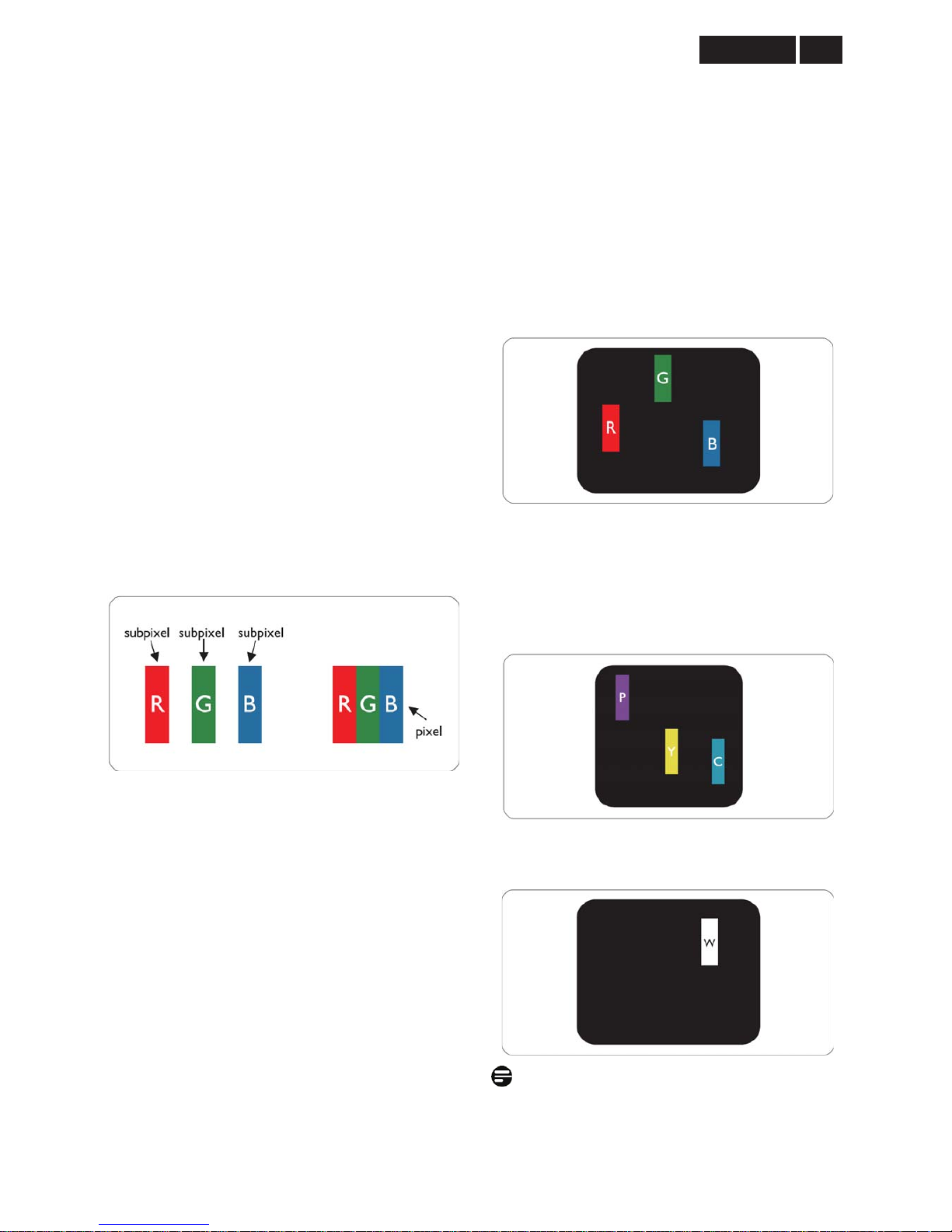
Pixels and Sub pixels
A pixel, or picture element, is composed of three sub
pixels in the primary colors of red, green and blue.
Many pixels together form an image. When all sub
pixels of pixel are lit, the three colored sub pixels
together appear as a single white pixel. When all are
dark, the three colored sub pixels together appear as a
signal black pixel. Other combinations of lit and dark
sub appear as single pixels of other colors.
Types of Pixel Defects
Pixel and sub pixel defects appear on the screen in
different ways. There are two categories of pixel
defects and several types of sub pixel defects within
each category.
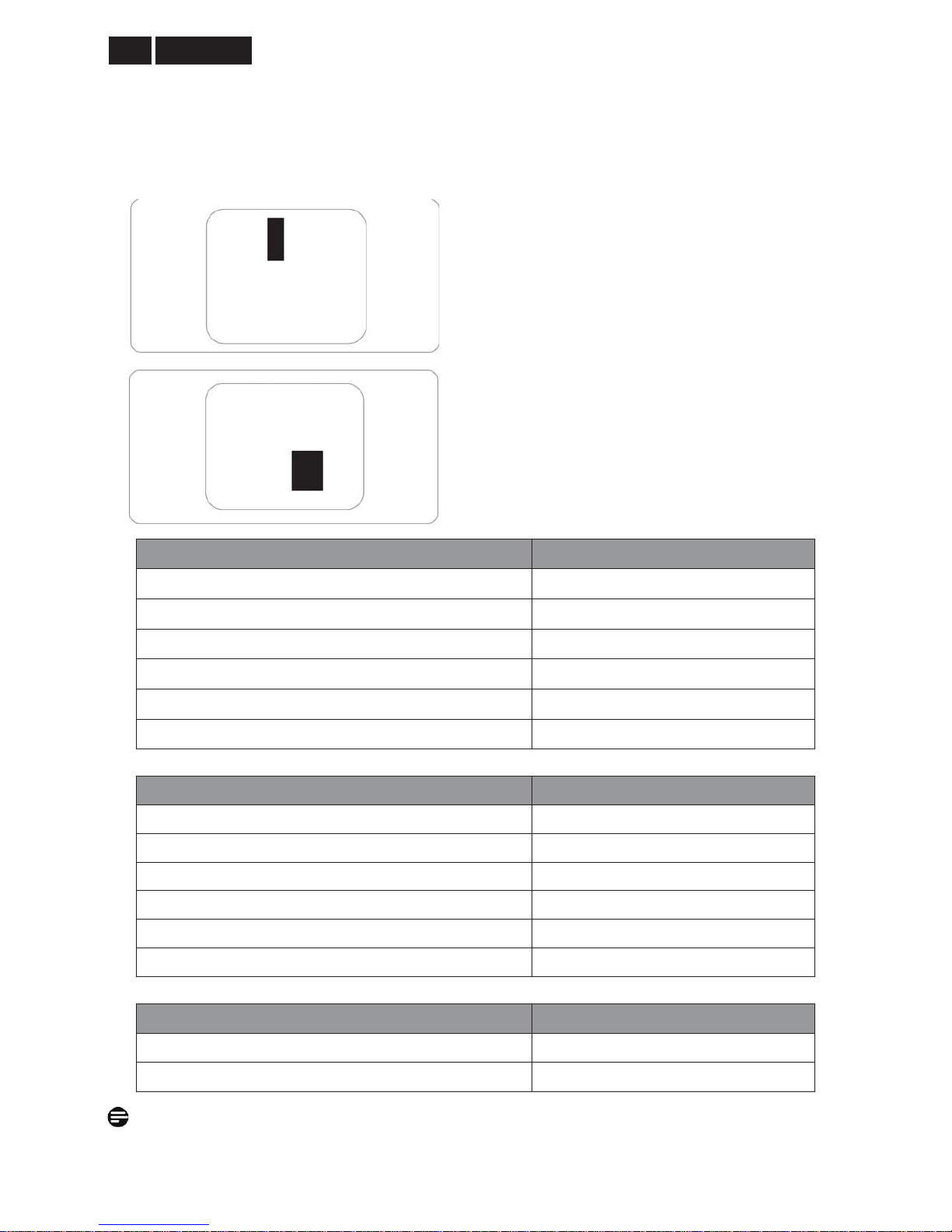
Bright Dot Defects Bright dot defects appear as pixel s
or sub pixels that are always lit or ‘on’. That is, a Bright
dot is a sub-pixel that stands out on the screen when
the monitor displays a dark pattern. There are three
types of bright dot defects:
One lit red, green or blue sub pixel
Two adjacent lit sub pixels:
- Red + Blue = Purple
- Red + Green = Yellow
- Green + Blue = Cyan (Light Blue)
Three adjacent lit sub pixels (one white pixel)
Note:
A red or blue bright dot must be more than 50 percent
brighter than neighboring dots while a green bright dot
is 30 percent brighter than neighboring dots.
!
!
Meridian 2
14
Black Dot Defects Black dot defects appea r as pixels
or sub pixels that are always dark or ‘off’. That is, a
dark dot is a sub-pixel that stands out on the screen
when the monitor displays a light pattern. There are
two types of black dot defects:
Proximity of Pixel Defects
Because pixel and sub pixels defects of the same type
that are near to one another may be more noticeable,
Philips also specifies tolerances for the proximity of
pixel defects.
Pixel Defect Tolerances
In order to qualify for repair or replacement due to pixel
defects during the warranty period, a TFT LCD p anel in
a Philips flat panel monitor must have pixel or sub pixel
defects exceeding the tolerances listed in the following
tables.
Bright Dot Defects Acceptable level
MODEL 191E2/191EL2
1 lit subpixel 3
2 adjacent lit subpixels 1
3 adjacent lit subpixels (one white pixel) 0
Distance between two bright dot defects* >15mm
Total bright dot defects of all types 3
Black Dot Defects Acceptable level
MODEL 191E2/191EL2
1 dark subpixel 5 or fewer
2 adjacent dark subpixels 2 or fewer
3 adjacent dark subpixels 0
Distance between two black dot defects* >15mm
Total black dot defects of all types 5 or fewer
Total Dot Defects Acceptable level
MODEL 191E2/191EL2
Total bright or black dot defects of all types 5 or fewer
Note:
1 or 2 adjacent sub pixel defects = 1 dot defect
15
Meridian 2
4.4 Failure Mode Of Panel
Failure description
Phenomenon
Vertical block defect
Vertical dim lines
Vertical lines defect
(Always bri
g
ht or dark)
Horizontal block defect
Horizontal dim lines
Horizontal lines defect
(Always bri
g
ht or dark)
Has bri
g
ht or dark pixel
Polarizer has bubbles
Polarizer has bubbles
Foreign material inside
polarizer. It shows liner or
dot shape.
Concentric circle formed
Bottom back light of LCD is
brighter than normal
Back light un-uniformity
Backli
g
ht has foreign material.
Black or white color, liner or
circular type
Quick reference for failure mode of LCD panel
this pa
g
e presents problems that could be made by LCD panel.
It is not necessary to repair circuit board. Simply follow the mechanical
instruction on this manual to eliminate failure by replace LC D panel.
!
!
Meridian 2
16
5. Block Diagram
5.1 Scaler Board
Flash Memory
EN25F20-100GCP
(U402)
Panel Interface
(CN301)
Crystal
14.31818MHZ
(
X401)
Keypad Interface
(CN401)
D-Sub Connector
(CN101)
EDID_WP
DDC1_SCL
DDC1_SDA
DVI Connector
(CN102)
EEPROM
AT24C02BN
(
U101)
EEPROM
AT24C02BN
(U102)
EDID_WP
DDCSCL2
DDCSDA2
Scaler IC TSUMU58NWHL-LF
(Include MCU, ADC, OSD)
(U401)
RX+/RXC+/-
RGB
H/Y Sync
17
Meridian 2
715G4411M01000004I
Flash Memory
A25L020AO-F
(U402)
Panel Interface
(CN303)
Crystal
14.31818MHZ
(
X401)
Keypad Interface
(CN402)
D-Sub Connector
(CN101)
DVI Connector
(CN102)
EEPROM
FM24C02A
(
U103)
EEPROM
FM24C02A
(U107)
Scaler IC TSUMU58NWHL-LF
(Include MCU, ADC, OSD)
(U401)
BKLT-EN
Setup-up Controller
TA9690GN
(IC801)
BKLT-VBRI
12V
!
!
Meridian 2
18
5.2 Adapter/Inverter/Converter Board
Inverter Board for 191E2
Converter Board for 191EL2
EN
A
Feedback Circuit
Transformer
(PT801, PT802)
Lamp
Output
Circui
t
PWM Control
ta9687GN
(IC801)
12V
DIM
MOSFET
APM4548A
5V
Protect Circuit
12V
EMI filter
Start Re sistor
(
R934, R906
)
PWM Control
(IC901)
Transformer
AC input
Bridge
Rectifier
Feedback
Circuit
Rectifier
Diodes
Power Switch
(Q901)
Photocoupler
(IC902)
ENA
Current Feedback
LED
panel
Boost Circuit
Setup-up Controller
TA9690GN
(IC801)
12V
DIM
OVP Circuit
19 Meridian 2
6. Schematic
6.1 Scaler Board (715G3598M0J000004W)
Remark: Parts position can be searched by using FIND function in PDF.
RX1N 5
C118
1000pF 50V
DVI_5V
ESD_VCC1
R137
4.7K1/16W
CMVCC1
RX2P 5
DSUB_V 5
DSUB_SDA
C117
220N16V
C119
1000pF 50V
V_Sync
RX2N
RX1P 5
DDC2_SCL 5
VGA_PLUG
DSUB_B+ 5
VGA_G+
RXCP 5
VGA_G+
VGA_G-
DSUB_R+ 5
DSUB_H 5
RX2P
CN101
D-SUB 15P
162738495
11
12
13
14
15
10
17 16
C115
100N 16V
R133
10K1/16W
C111
47N 16V
FB102
BEAD
1 2
DET_CABLE 5
R112
75OHM1/16W
DDC1_SDA5
DDC2_SDA
R110
470OHM1/16W
CMVCC1
RX0P 5
H_Sync
R117
47 OHM 1/16W
VGA_R-
DSUB_SDA
R123
10K1/16W
VCC3.3
RX0P
RX1P
FB105
300 OHM
U105
AZC199-04S
123 4
5
6
I/O1
GND
I/O2 I/O3
VDD
I/O4
U103
AZC199-04S
123 4
5
6
I/O1
GND
I/O2 I/O3
VDD
I/O4
R109
47 OHM 1/16W
R136
10K1/16W
R131 10OHM1/16W
DSUB_5V
DDC_WP5
C109
5PF 50V
R128 10OHM1/16W
C103
22P 50V
ESD_VCC1
DVI_HPD
VGA_B+
D101
BAV70
3
1
2
ESD_VCC
FB101
BEAD
1 2
RX2N 5
DSUB_G- 5
RXCP
R126 10OHM1/16W
C124
100N 16V
VGA_B+
VGA_R+
DVI_HPD
R103 1K1/16W
R107
2.2K1/16W
DDC1_SCL
D102
BAV70
3
1
2
ZD101
RLZ5.6B
RXCN 5
VGA_R+
VGA_PLUG
R111
10OHM1/16W
ESD_VCC1
R125
4.7K1/16W
RX0N 5
DDC2_SDA 5
DSUB_5V
R129 10OHM1/16W
U106
AZC199-04S
123 4
5
6
I/O1
GND
I/O2 I/O3
VDD
I/O4
R134 10OHM1/16W
VGA_R+
VGA_PLUG
Input
DSUB_G+ 5
R115
10OHM1/16W
RX1N
C107
1000pF 50V
FB106 300 OHM
C121
1000pF 50V
R127 10OHM1/16W
C114
47N 16V
R119 100OHM1/16W
DSUB_R- 5
VGA_B-
R105
10OHM1/16W
C110
47N 16V
U104
AZC199-04S
123 4
5
6
I/O1
GND
I/O2 I/O3
VDD
I/O4
C106
47N 16V
R138
4.7K1/16W
R124
4.7K1/16W
DSUB_B- 5
DDC1_SDA
FB103
BEAD
1 2
DDC1_SCL5
VGA_G+
CN102
JACK
1
2
3
4
5
678
9
101112
13
141516
17
18
19
20
212223
24
26
25
DAT2-
DAT2+
2/4shield
DAT4-
DAT4+
DDC SCL
DDC SDA
VSYNC
DAT1-
DAT1+
1/3shield
DAT3-
DAT3+
+5V
SYNC GND
HPD
DAT0-
DAT0+
0/5shield
DAT5-
DAT5+
clk shield
clk+
clk-
GND
GND
U102
AT24C02BN-SH-T
123
45
678
A0A1A2
VSSSDA
SCLWPVCC
R116
75OHM1/16W
R130 10OHM1/16W
R120 10K1/16W
DVI_5V
VGA_R-
U101
AT24C02BN-SH-T
123
45
678
A0A1A2
VSSSDA
SCLWPVCC
VGA_B-
R135
10K1/16W
C104
22P 50V
R106
2.2K1/16W
DDC2_SCL
DDC2_SDA
R114
47 OHM 1/16W
C102
47N 16V
V_Sync
RX0N
ESD_VCC
C105
5PF 50V
DDC1_SCL
C116
220N16V
ESD_VCC1
VGA_B+
DSUB_SCL
R101
100OHM1/16W
CMVCC13,4,5,8
R139
6.8K1/16W
R104 1K1/16W
DSUB_SCL
DSUB_SOG 5
DDC2_SCL
R102 0R05 1/10W
FB104
300 OHM
RXCN
R118 100OHM1/16W
DDC1_SDA
R108
75OHM1/16W
ESD_VCC
VGA_G-
C120
1000pF 50V
R132 10OHM1/16W
DDC_WP5
H_Sync
C113
5PF 50V
R113
100OHM1/16W
U107
AZC199-04S
123 4
5
6
I/O1
GND
I/O2 I/O3
VDD
I/O4
C108
47N 16V
!
20
Meridian 2
Remark: Parts position can be searched by using FIND function in PDF.
RXO2-
R304
22K1/16W
LVB0M
RXO2+
PB[0..9]
LVBCKM
LVA1P
S
LVB1M
RXE1-
RXEC+
PANEL_VCC
PA[0..9]
PA7
RXE2+
LVBCKM
LVB3M
AO3401L
C304
100N 16V
CMVCC12,4,5,8
PA[0..9]5
PB3
RXE2-
R303
4.7K1/16W
PA8
LVBCKP
PB9
PA3
LVB1P
PB2
RXE1+
C302
22UF 16 V
PB7
LVB2P
FB301
120 OHM
1 2
LVA0M
PA5
C305
1uF 16V
R301
220 OHM 1/4W
RXOC+
RXO1+
LVA3P
PA4
PA2
PA1
PB0
RXE0+
D
RXEC-PB8
LVB3P
Output
R305
10K1/16W
PB5
R308
10K1/16W
CMVCC1
LVB1M
LVA0M
RXE3+
1
RXO3-
R306
100K1/16W
CN301
CONN
24681012141618202224262830
13579
111315171921232527
29
3132
LVA2P
LVB3P
LVB2M
LVA0P
LVB0P
Q302
LMBT3904LT1G
C303
220N16V
LVA1M
RXO1-
PPWR_ON#5
CMVCC1
LVB0M
PANEL_VCC
3
LVA3M
LVB2P
Q301
AO3401
LVA1M
LVA2M
LVA3M
RXO0-
LVA2M
PA6
LVACKM
PB6
LVACKM
PB4 RXO3+
C301
100N 16V
LVACKP
LVBCKP
RXOC-
RXE3-
PB[0..9]5
LVA1P
LVACKP
LVA0P
2
PA9
LVB2M RXE0-
R302
220 OHM 1/4W
LVA3P
R307
NC
G
RXO0+
PA0
LVA2P
PB1
LVB0P
LVB1P
U301
NC/AO4411
1
2
3
4
8
7
6
5
S
S
S
G
D
D
D
D
LVB3M
21 Meridian 2
Remark: Parts position can be searched by using FIND function in PDF.
+12V
C702
100N 16V
C719
100nF 25V
R704 22K1/ 16W
D701
SM340A
1 2
C717
100N 16V
CMVCC1 2,3,5,8
CMVCC1
FB701
BEAD
1 2
Dropout voltage
must < 0.8V @ 400mA
on_BACKLIGH T 5
Q701
LMBT3904LT1G
SOT 223
CN702
CONN
123456789
10
1112
D704
SM340A
12
D708
SM340A
12
C723
10uF 25V
U704
3 2
1
VI VO
GND
C706
100N 16V
CN701
JACK
321
+12V
L701 22UH
R706
100OHM1/16W
+
C718
180uF 16V
BKLT-VBRI
C707
22UF 16V
R711
33K 1/16W
CMVCC1
R708
NC/0R 05 1/10W 5%
U705
MP1584EN
123
45
678
9
SW
EN
COMP
FBGND
FREQ
VIN
BST
Therm al P a d
+
C716
470uF 10V
C721
100N 16V
SOT 223
C715
1N 50V
BKLT-EN
R707
0R05 1/10W
R703
10K1/16W
VCC3.3
U702
G1117-33T43UF
1
2
3
ADJ(GND )
VOUT(TAB)
VIN
SOT 252
R702
10K1/16W
R712
100K1/16W
C708
100N 16V
VCC3.3
C714
1N 50V
C710
1N 50V
C705
100N 16V
D707
SM340A
12
R726
100K1/16W
+12V
C713
100nF 25V
R727
180K 1/16W 5%
C709
100N 16V
R714
1K3 +-1% 1/16W
adj_BACKLIGHT 5
D703
SM340A
12
C722
150pF 50V
CMVCC1
U703
NC/AZ 1117D-1. 8-E1
23
1
OUTIN
GND
ZD702
NC/RLZ6.2B
1 2
R713
6K8 1/16W 1%
U701
3 2
1
VI VO
GND
C711
1N 50V
CMVCC1
C704
22UF 16V
Dropout voltage
must < 0.8V @ 600mA
BKLT-EN
FB703
0R05 1/10W
C712
100nF 25V
CMVCC1
VCC1.8
SOT 252
Power
BKLT-VBRI
R705
10K1/16W
CMVCC1
C720
10uF 25V
!
22
Meridian 2
Remark: Parts position can be searched by using FIND function in PDF.
PB6
C414
100N 16V
R425 NC/100OH M1/16W
Scaler
KEY1
LED_ORANGE
PB2
Max condition for LED:
1. Vcc = 3.3 V
2. Current = 12 mA
FW need to be
modified.
KEY2
PB4
For All model
C408
100N 16V
U402
PA9
PB8
C421 47pF 50V
VCC1. 8
CMVCC1
RX2N2
R402
2.2K1/16W
R433
3.9K1/16W
010A
VCC3.3
RX1N2
KEY2
Befor AOC ID2007 OSD
C415
100N 16V
VMPLL
DSUB_G-2
LED_R
U402
EN25F20-100GCP
123
4 5
678
CS#DOWP#
VSS DI
CLK
HOLD#
VCC
VDVI
PA3
C401
220N16V
C406
100N 16V
C422
100N 16V
18 pF
VCC3.3
SST
RX0P2
PA1
PB0
R406
22K1/16W
DSUB_V2
C417
100N 16V
POWER_KEY#
LED_R
C416
100N 16V
X401
DSUB_B+2
adj_BACKLIGHT 4
R431
NC/3.9K OHM +-1% 1/16W
Eon
VDDC
FB408
120 OHM
1 2
C404
100N 16V
AVDD
C411
100N 16V
ǂ㬐
(93G 22-53B-H)
RXCN2
RX0N2
DDC1_SDA2
R416 100OHM1/16W
Cs and Cd (C420, C421)
LED_G
C413
100N 16V
C418
NC 100N 16V
C407
100N 16V
FB402
300OHM
VCC3.3
TSUMU58NWHL-LF-1
232021182219172728
152625
373938
40
47
86
59
96
97
6061626364
65
676869707172737477
78
585554
2
5
346
789
101213
11
29
33
24
56
53
52
81
51
30
31
100
1
93
14
75
3548858889909192949599
43
44
84
41
42
98
16
32
49
66
82
34
50
57
76
79
83
80
87
364546
RIN0P
GIN0P
SOGIN0
BIN0P
RIN0M
GIN0M
BIN0M
HSYNC0
VSYNC0
REXT
REFP
REFM
SDO
SCK
SCZ
SDI
PWM2/GPIO_P24
PWM1/GPIO_P25
LVACKM
XOU T
XIN
LVA2P
LVA2M
LVA1P
LVA1M
LVA0P
LVA0M
LVB3P
LVB3M
LVBCKP
LVBCKM
LVB2P
LVB2M
LVB1P
LVB1M
LVB0P
LVB0M
LVACKP
LVA3M
LVA3P
GND
GND
RX2P
RX2N
RX1P
RX1N
AVDD_33
RX0P
RX0N
RXCKP
RXCKN
GND
GND
GND
AVDD_33
VDDP
MODE
NC
VCTRL
VDDC
DDCA_SDA/ RS232_TX
DDCA_SCL/ rs232_RX
DDCD_SDA
DDCD_SCL
PWM0/GPIO_P26
AVDD_33
VDDP
GPIO_P15/PWM0
GPIO_P27/PWM1
GPIO_P12
GPIO_P00/SAR1
GPIO_P01/SAR2
GPIO_P02/SAR3
GPIO_P06
GPIO_P07
GPIO_P13
GPIO_P14
GPIO_P16/PWM2
GPIO_P11/I2C_MDA
GPIO_P10/I2C_MCL
RST
GPIO_P23
GPIO_P22
AVDD_33
AVDD_33
VDDP
VDDP
VDDC
VDDC
VDDC
GND
GND
GND
GND
GND
BYPASS
GPIO_P17/SAR0
GPIO_P40
GPIO_P41
GPIO_P42
ZD401
NC/RLZ 5.6B
LED_ORANGE
DDC1_SCL2
LED_R
R432
3.9K1/16W
LVDS
PA0
Q401
LMBT3904LT1G
R404
4.7K1/16W
VCC3. 3
VDDP
AUDIO_MUTE 8
RX1P2
LED_ORANGE
VDDP
VCC3.3
DET_CABLE 2
FB401
300OHM
VDVI
KEY1
ZD403
NC/RLZ 5.6B
R405
0R05 1/10W
CMVCC12,3,4,6, 8
DSUB_H2
C434
NC/0 . 1uF 16 V
PA[0..9]
VCC3. 3
For ID2008 ID2009
X'TAL
VDDC
R401 390R 1/16W 1%
C420 47pF 50V
CN402
CONN
123
4
65
SST
DSUB_G+2
R420
4.7K1/16W
R417 100OHM1/16W
VCC3.3
R414
0R05OHM1/16W
PA6
DSUB_R+2
WP
PB5
R423 0R05OH M1/16W
47 pF
VCC3. 3
R428 100OHM1/16W
R419
10K1/16W
Normal Function : CL = Cs + ((Cg*Cd)/(Cg+Cd))
CMVCC1
LED_G
VCC3. 3
DDC2_SDA2
R436 100OHM1/16W
FB406 0R
PB7
DSUB_SOG2
RX2P2
DDC2_SCL2
FB404
300OHM
C433
NC/0 . 1uF 16 V
U402
CL of SPEC
Q403
LMBT3906LT1G
1
23
020A
AVDD
⨝㑶
(93G 22-53-J)
VCC3.3
R413
NC/0R05 1/ 16W
VCC3.32,4
Volume 8
C435
NC/0 . 1uF 16 V
WP
R407
10K1/16W
C412
100N 16V
LED_GRN/BLUE
PB3
ZD402
NC/RLZ 5.6B
DSUB_B-2
PB[0..9]
PB9
X401
14.31818MHZ/32PF
1 2
R421
100K1/16W
VCC1.84
VPLL
CMVCC1
VPLL
R412
10K1/16W
on_BACKLIGHT 4
PB1
FB405
0R
AVDD
PB[0.. 9] 3
C405
100N 16V
C419
10U 10V
U402
R438
10K1/16W
POWER_KEY#
C409
100N 16V
27 pF
PA5
VMPLL
C432
100N 16V
P.S : Assume Cs = 4 pF
RXCP2
R403
0R05 1/10W
C403
100N 16V
R437 100OHM1/16W
020
C410
100N 16V
R415 100OHM1/16W
DSUB_R-2
CMVCC1
MSDA
C402
10U 10V
Eon
R439
10K1/16W
C431
100N 16V
PA[0.. 9] 3
MSCL
Q402
LMBT3906LT1G
1
23
CN401
CONN
1234567
89
PA7
PA8
FB409
NC/120 OHM
1 2
32 pF
DDC_WP 2
PA4
PA2
R409 100OHM1/16W
For user data, WB, EDID,
HDCP are saved in
Flash.
PPWR_ON#3
LED_GRN/BLUE
23 Meridian 2
715G4411M01000004I
Remark: Parts position can be searched by using FIND function in PDF.
RX1N
C122
100N 16V
RX0P 5
CMVCC1
DVI_HPD
C107
47N 16V
R105
75 OHM +-5% 1/16W
ESD_VCCD
VGA_B+
RX0N
R123
4.7K1/16W
DDC2_SDA
C104
22P 50V
CN102 JACK
1
2
3
4
5
678
9
10
11
12
13
141516
17
18
19
20
212223
24
26
25
DAT2-
DAT2+
2/4shield
DAT4-
DAT4+
DDC SCL
DDC SDA
VSYNC
DAT1-
DAT1+
1/3shield
DAT3-
DAT3+
+5V
SYNC GND
HPD
DAT0-
DAT0+
0/5shield
DAT5-
DAT5+
clk shield
clk+
clk-
GND
GND
U104
AZC199-04S
12345
6
I/O1
GND
I/O2
I/O3
VDD
I/O4
DSUB_V 5
VGA_R+
R136 10K 1/ 16W 5%
R114
100OHM1/16W
DSUB_R- 5
CN101
D-SUB 15P
162738495
11
12
13
14
15
10
17 16
FB106
300R
1 2
DSUB_SDA
R113 47 OHM 1/16W
R134
4.7K1/16W
VGA_B-
R137 6.8K1/16W
FB104
300R
DSUB_SOG 5
DDC1_SDA
DSUB_SDA
DDC1_SDA
VGA_G-
R119 100OHM1/16W
R122
4.7K1/16W
C105
47N 16V
FB105 300R
ESD_VCCD
VGA_PLUG
R110 10OHM1/16W
C106
NC/1nF 50V
RXCP
RX2P
VGA_B-
R107
2.2K1/16W
RX1N 5
DET_CABLE 5
VGA_G+
FB102
BEAD
1 2
CMVCC2
DDC2_SCL
R128 10OHM1/16W
R117 47 OHM 1/16W
R126 10OHM1/16W
RX2P 5
VGA_G+
DSUB_G+ 5
U106
AZC199-04S
123 4
5
6
I/O1
GND
I/O2 I/O3
VDD
I/O4
C112
47N 16V
R104 1K 1/ 16 W 5%
R127 10OHM1/16W
V_Sync
C113
100N 16V
RXCN
C102
47N 16V
DSUB_G- 5
DSUB_SCL
C108
100N 16V
VCC3.3
DVI_5V
DSUB_R+ 5
DVI_5V
DDC2_SDA
FB101
BEAD
1 2
DDC2_SCL
U102
AZC199-04S
1234
5
6
I/O1
GND
I/O2I/O3
VDD
I/O4
R121
10K 1/16W 5%
ESD_VCC
VGA_PLUG
C101
22P 50V
C109
5PF 50V
DDC1_SCL5
DDCD_WP5
R112
75 OHM +-5% 1/16W
FB103
BEAD
1 2
R129 10OHM1/16W
VGA_B+
R118 100OHM1/16W
R102 10OHM1/16W
CMVCC1
R124 10OHM1/16W
VGA_R-
VGA_PLUG
R133
10K 1/16W 5%
RX2N 5
DSUB_5V
RX2N
R132
10K 1/16W 5%
C120
100N 16V
RX1P 5
C111
100N 16V
DVI_HPD
DDC2_SDA 5
R135
4.7K1/16W
ESD_VCC
VGA_R+
R106
2.2K1/16W
DSUB_5V
U105
AZC199-04S
123 4
5
6
I/O1
GND
I/O2 I/O3
VDD
I/O4
C110
47N 16V
R101 0R 05 1/ 10WH_Sync
VGA_G-
DSUB_B- 5
ESD_VCCD
C119
220nF 16V
R115 10OHM1/16W
C103
5PF 50V
R130 10OHM1/16W
CMVCC13,4,5
VGA_R-
R125 10OHM1/16W
D102
BAV70
3
1
2
DDCV_WP5
R103 1K 1/ 16 W 5%
C114
5PF 50V
VGA_B+
RX0P
C116
100N 16V
DSUB_B+ 5
V_Sync
R131 10OHM1/16W
VGA_R+
U103
FM24C02A
123
45
678
A0A1A2
GNDSDA
SCLWPVCC
R109 NC/470OHM1/16W
R120 10K 1/16W 5%
DSUB_SCL
ZD101
RLZ5.6B
DDC2_SCL 5
U107
FM24C02A
123
45
678
A0A1A2
GNDSDA
SCLWPVCC
DDC1_SCL
R116
75 OHM +-5% 1/16W
RXCP 5
H_Sync
VGA_G+
DDC1_SCL
U101
AZC199-04S
12345
6
I/O1
GND
I/O2
I/O3
VDD
I/O4
R108 47 OHM 1/16W
C121
100N 16V
DSUB_H 5
C117
1nF 50V
RXCN 5
ESD_VCCD
R111
100OHM1/16W
D101
BAV70
3
1
2
RX0N 5
DDC1_SDA5
ESD_VCC
RX1P
C115
47N 16V
C118
220nF 16V

!
24
Meridian 2
Remark: Parts position can be searched by using FIND function in PDF.
LVB1M
RXE2-
PA[0..9]
LVBCKM
RXEC-
LVA2M
PB0
LVACKM
Q302
LMBT3904LT1G
RXO3+
RXO2-
LVBCKP
C305
1uF 16V
PA4
LVA1P
D
RXOC-
PB5
LVB3M
RXE0+
PA7
RXE0+
Q301
AO3401
LVACKP
RXO0+
R302
220 OHM 1/4W
PANEL_VCC
LVA2P
1
CMVCC1
RXEC+
PB[0..9]5
LVB2M
LVB2P
RXO2-
RXOC+
LVA0M
C302
100N 16V
CMVCC1
RXO1-
LVA1M
LVA2M
RXO3+
R306 22K1/16W
3
LVB2P
PB1
LVBCKM
LVA1P
LVB0M
PPWR_ON#5
PA0
RXE3+
RXO3-
LVA3M
PB8
RXO1+
RXE2+
RXE3-
LVA0P
RXE1+
RXO0-
RXO0+
RXE1-
PA1
R305 100K1/16W
RXO0-
PB4
PA3
PANEL_VCC
PA5
LVA3M
FB301
120 OHM
1 2
LVA2P
R301
220 OHM 1/4W
2
PA8
C301
22UF 16V
LVB0M
RXO2+
RXO3-
LVB1P
LVA1M
LVB3P
PA2
LVACKM
PB6
LVB0P
G
U301
NC/AO4411
1
2
3
4
8
7
6
5
S
S
S
G
D
D
D
D
CN303
CONN
246810
12
14
16
18
20
22
24
26
28
30
13579
11
13
15
17
19
21
23
25
27
29
PA6
RXEC-
R304
10K 1/16W 5%
LVB1P
PB7
PB9
LVB3M
LVA0M
RXEC+
RXE0-
R307
4.7K1/16W
PA9
LVA3P
RXO2+
LVB3P
S
LVACKP
RXE3+
RXO1+
C303
220nF 16V
RXE0-
CMVCC12,4,5
RXE1-
RXE2-
LVB1M
RXO1-
AO3401L
LVB2M
PA[0..9]5
PB[0..9]
RXE1+
PB2 LVBCKP
R308
10K 1/16W 5%
RXOC+
RXE3-
LVB0P
RXOC-
C304
100N 16V
PB3
LVA3P
RXE2+
LVA0P
25 Meridian 2
Remark: Parts position can be searched by using FIND function in PDF.
C707
22UF 16V
SOT 252
C702
100N 16V
VCC3.3
D702
SM340A
12
adj_BACKLIGHT 5
C704
22UF 16V
C717
100nF 25V
C716
10uF 25V
on_BACKLIGHT 5
+12V
R709
33K 1/16W 5%
BKLT-EN6
C714
100N 16V
CMVCC1 2,3,5
CN701
JACK
321
Q701
LMBT3904LT1G
VCC1.8
U704
NC/AZ1117D-1.8-E1
23
1
OUTIN
GND
+
C709
470uF 10V
SOT 252
R703 22K1/16W
BKLT-VBRI
D703
SM340A
12
CMVCC1
U702
3 2
1
VI VO
GND
+
C715
180uF 16V
L701 22uH
VCC1.8 5
D701
SM340A
12
+12V 6
R704
10K 1/16W 5%
U703
3 2
1
VI VO
GND
ZD701
NC/RLZ6.2B
1 2
R701
10K 1/16W 5%
R706
100K1/16W
R708
100K1/16W
CMVCC1
R705 100OHM1/16W
VCC3.3 2,5
BKLT-EN
C706
100N 16V
C708
100nF 25V
C710
2.7NF 50 V
BKLT-VBRI6
R710
300K
CMVCC1
VCC3.3
C713
10uF 25V
U701
G1117-33T43UF
1
2
3
ADJ(GND)
VOUT(TAB)
VIN
C703
100N 16V
CMVCC1
SOT 223
VCC3.3
C705
100N 16V
D705
SM340A
1 2
R711
1.3K 1%
SOT 223
C718
1nF 50V
FB701
BEAD
1 2
FB702
0R05 1/10W
R702
10K 1/16W 5%
U705 MP1584EN
123
45
678
9
SW
EN
COMP
FBGND
FREQ
VIN
BST
Ther m a l P a d
C711
150pF 50V
R707
6K8 1%
C701
100N 16V
D704
SM340A
12
FB801
0R05 1/4W
C712
1nF 50V
!
26
Meridian 2
Remark: Parts position can be searched by using FIND function in PDF.
PB[0..9] 3
PB3
R405
4.7K1/16W
C403
100N 16V
C426
NC/100N 16V
C415
100N 16V
R430
3.9K1/16W
VCC3.3
LED_GRN/BLUE
ZD403
RLZ5.6B
VDDC
FB404 NC/120 OH M1 2
C401
100N 16V
R403
0R05 1/16W
VPLL
CMVCC1
FB403
300OHM
C421
100N 16V
DDCV_WP 2
LED_R
LSDA
R416 0R01 1/10W
VCC3.3
DSUB_H2
DSUB_R+2
PB[0..9]
KEY1
C423
100N 16V
R428
3.9K1/16W
R411 0R01 1/10W
R431 100OHM1/16W
R426 NC/100OHM1/16W
EE_WP R404
2K2 1/16W 5%
R421 NC/100OH M1/16W
C410
100N 16V
DSUB_B+2
PB0
R427 NC/100OH M1/16W
C416
220nF 16V
adj_BACKLIGHT4
PA0
CN401
NC/CONN
123
4
CMVCC12,3,4
R417
100K1/16W
C406
10U 10V
RXCN2
R408 100OHM1/16W
R422 0R05 1/16W
LED_GRN/BLUE
C402
100N 16V
CN402
CONN
1234567
U402
A25L020AO-F
123
4 5
678
S
DOWVss D IO
C
HOLD
Vcc
PA8
C414
100N 16V
RX0P2
PA6
R409 10K 1/ 16W 5%
VCC1.8
X401
14.31818MHZ/32PF
1 2
FB405 NC/120 OH M1 2
LED_ORANGE
LED_ORANGE
CMVCC1
VDVI
LED_G
C404
100N 16V
C418 47pF 50V
DSUB_SOG2
DSUB_R-2
FB401
300OHM
KEY1
C417 10U 10V
R413 4.7K1/16W
RXCP2
ZD401
RLZ5.6B
C420
100N 16V
Q401
LMBT3906LT1G
1
23
R410
10K 1/16W 5%
R415 100OHM1/16W
R419 NC/100OH M1/16W
R423
NC/10K1/16W
PA9
VCC3.32,4
LVDS
RX1P2
VDDP
POWER_KEY#
DSUB_G-2
PPWR_ON# 3
PA7
C411
100N 16V
VDDP
CMVCC1
R412 100OHM1/16W
R414 100OHM1/16W
VCC3.3
U403
NC/AT24C04BN
123
45
678
A0A1A2
GNDSD A
SCLWPVCC
KEY2
WP
R401 390R 1/ 16W 1%
RX0N2
CMVCC1
LSCL
R425
NC/10K1/16W
C409
100N 16V
LED_G
DSUB_V2
R420 0R05 1/16W
LSCL
AVDD
DET_CABLE 2
WP
C405
100N 16V
VDDC
PB4
LED_R
R402
NC/0R 05 1/ 16W
VCC3.3
C425
NC/100N 16V
VMPLL
VCC3.3
VCC3.3
DDC1_SCL2
VCC3.3
C408
100N 16V
AVDD
PB1
LED_R
R406 NC/100OHM1/16W
PA5
PB6
RX1N2
PA1
R429
3.9K1/16W
C413
100N 16V
FB402
300OHM
DDC2_SDA2
VMPLL
Q402
LMBT3906LT1G
1
23
PA[0..9] 3
VPLL
on_BACKLIGHT 4
KEY2
ZD402
RLZ5.6B
DDCD_WP 2
PB2
C422
100N 16V
VDVI
PB8
LSDA
PB9
R424
NC/10K1/16W
R407 100OHM1/16W
C407
100N 16V
C424
100N 16V
VCC1.84
VCC3.3
DDC2_SCL2
DSUB_G+2
C412
100N 16V
C419 47pF 50V
DDC1_SDA2
R418 100OHM1/16W
PB7
VCC3.3
PB5
PA4
PA2
RX2P2
RX2N2
DSUB_B-2
PA3
POWER_KEY #
AVDD
EE_WP
TSUMU58NWHL5-LF
232021182219172728
15
26
25
373938
40
47
86
59
96
97
6061626364
65
676869707172737477
78
585554
2
5
346
789
101213
11
29
33
24
56
53
52
81
51
30
31
100
1
93
14
75
3548858889909192949599
43
44
84
41
42
98
16
32
49
66
82
34
50
57
76
79
83
80
87
364546
RIN0P
GIN0P
SOGIN0
BIN0P
RIN0M
GIN0M
BIN0M
HSYNC0
VSYNC 0
REXT
REFP
REFM
SDO
SCK
SCZ
SDI
PWM2/GPIO_P24
PWM1/GPIO_P25
LVACKM
XOU T
XIN
LVA2P
LVA2M
LVA1P
LVA1M
LVA0P
LVA0M
LVB3P
LVB3M
LVBCKP
LVBCKM
LVB2P
LVB2M
LVB1P
LVB1M
LVB0P
LVB0M
LVACKP
LVA3M
LVA3P
GND
GND
RX2P
RX2N
RX1P
RX1N
AVDD_33
RX0P
RX0N
RXCKP
RXCKN
GND
GND
GND
AVDD_33
VDDP
MODE
NC
VCTRL
VDDC
DDCA_SDA/RS232_TX
DDCA_SCL/rs232_RX
DDCD_SDA
DDCD_SCL
PWM0/GPIO_P26
AVDD_33
VDDP
GPIO_P15/PWM0
GPIO_P27/PWM1
GPIO_P12
GPIO_P00/SAR1
GPIO_P01/SAR2
GPIO_P02/SAR3
GPIO_P06
GPIO_P07
GPIO_P13
GPIO_P14
GPIO_P16/PWM2
GPIO_P11/I2C_MDA
GPIO_P10/I2C_MCL
RST
GPIO_P23
GPIO_P22
AVDD_33
AVDD_33
VDDP
VDDP
VDDC
VDDC
VDDC
GND
GND
GND
GND
GND
BYPASS
GPIO_P17/SAR0
GPIO_P40
GPIO_P41
GPIO_P42
VCC3.3
PA[0..9]
27 Meridian 2
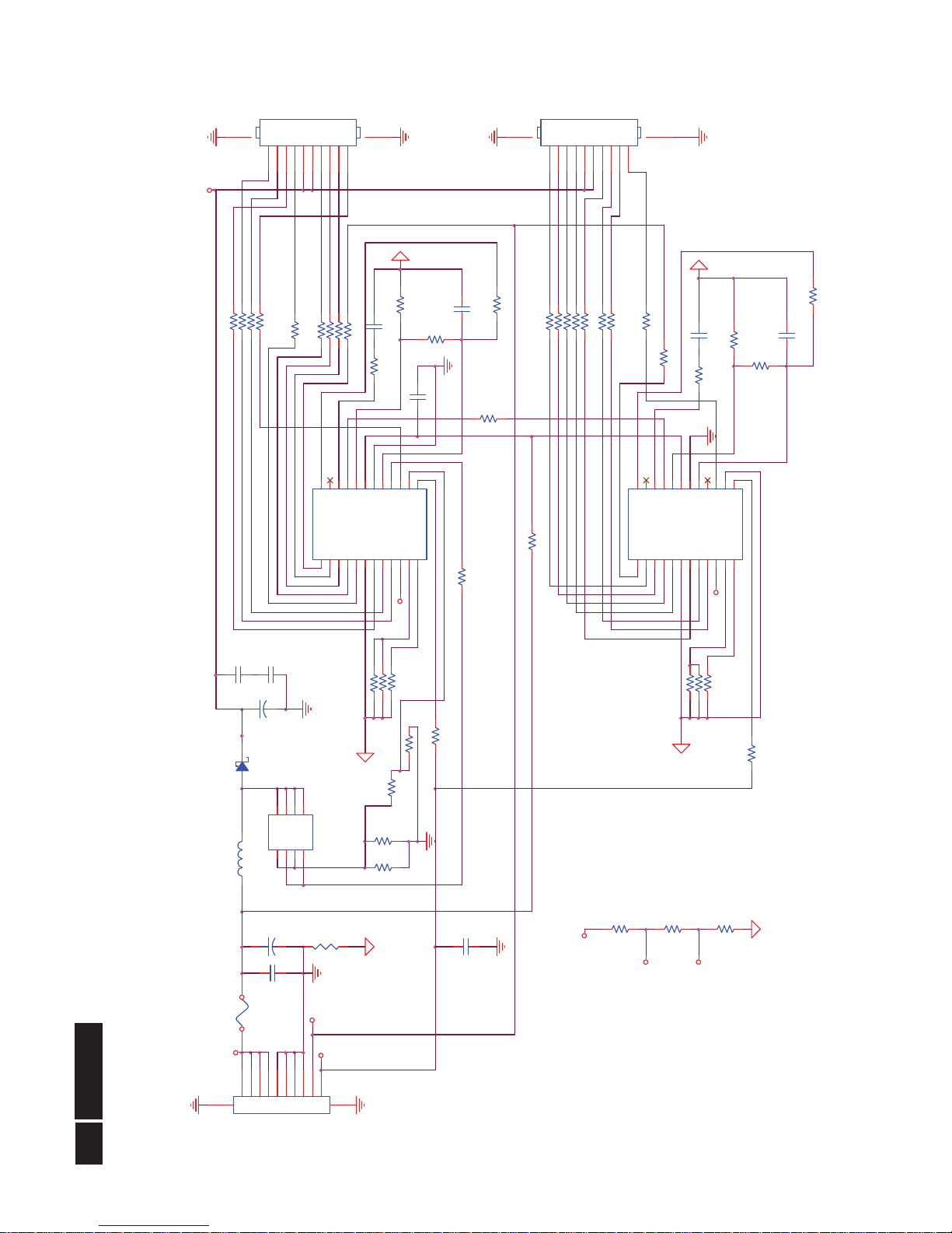
Remark: Parts position can be searched by using FIND function in PDF.
C805
0.47uF 16V
R821
LED7
NC
con16
R829 NC
+
C813
270UF 25V
XX K
NC
NC
CPT CLAA185WA04
1R
con2
R812
100R 1/10W 5%
NC
NC
NC
0R
NC
con6
LED6
2.2uNC
NC
1R
R833
39K
NC
con1
R810
1K 1/10W 5%
AUO M185XWV01 V6
NC
NC
LED14
AUO M215HW01 V6
con12
1R
NC
NC
NC
30K
NC
R820
NC
NC
LED1
100R
NC
1R
100K
NC
LED12
R832 1R 1/10W 5%
NC
NC
NC
R834
LED3
NC
R831
NC
R803
NC
+
C804
4.7UF 100V
NC
NC
1R
0R
1K
Vout
NC
NC
1R
NC
NC
NC
NC NC
NC
NC
0R
XX KNC
NC
1R
OVP1
C806
2U2 25V
52.3K
NC
NC
CMO M215H3-LA1
LED8
NC
R803
NC
LED8
LED2
LED2
R854
0R05 4A 1/4W
NC
NC
NC
0R
NC
1R
NC
LED13
con18
R827 NC
C810
100N 50V
10K
1R
1R
NC
C816
IC801
TA9690LN-A1-0-TR
1
2
3
4
5
6
789
101112
13
14
15
16
17
18
19202122232425
ISEN4
GNDA
ISEN5
ISEN6
ISEN7
ISEN8
OVP
ISETRTENA
ISW
NC
LDR
VREF
GNDP
VIN
SEL
COMP
SSTCMP
STATUS
PWM
ISEN1
ISEN2
ISEN3
E-PAD
NC
R815
LED4
10K
1R
NC
NC
con1
LED15
R848 0R05 1/10W
NC
NC
R851
R839
NC
con17
LED17
C803
100N 50V
NC
SEC LTM185AT04
R804 24K +-1% 1/10W
C814
100P 50V
NC
1R
NC
NC
NC
NC/CN801
CONN
1
2
NC
NCR847
NC
1R
NC 1K
NC
NC
Vout
CN803
NC/CONN
123456789
1011121314151617181920
1R
NC
R840
LED15
LED11
R852 0R05 1/10W
R823
100R
con13
LED7
NC
0R
AUO M185XWV01 V6
47K
24K
R850 0R05 1/10W
0R
CPT CLAA215FA04
V2
NC
1R
NC
R821 NC
NC
NC
NC
R830
R817
NC
1R
C808
NC
LED1
C801
100N 50V
SEC LTM185AT04
NC
BKLT-EN4
con6
R822
1M 1/8W 5%
R834 NC
0.47u
NC
R827
1R
NC
0R
LGD
LM215WF4-TLA1
1R
R835
R849 NC(0R 05 1/ 10W )
R836 NC
NC
NC
XX K
1R
NC
NC
NC
NC
1R
NC
0R
NC
R828
con8
1K
NC
R841 NC
C807
2.2U16V
LGD
LM215WF4-TLA1
NC
NC
NC
R825
15OHM 1/10W +/-5%
C809
NC
1R
1R
LED5
R809
100K 1/10W 5%
NC
R848
NC
NCNC
con11
L801 47UH
1R
NC
1R
1R
NC
con5
LED5
NC
NC
NC
NC
NC
LED17
R837 NC
NC
NC
10K
NC
R819
1K
con16
LED14
R853
0R05 4A 1/4W
1R
NC
0R
NC
C815
0.33uF 16V
R846 0R05 1/10W
NC
NC
NC
NC
NC
NC
R842 240K 1/10W 5%
1R
NC
con7
R831 NC
1R
NC
1R
NC 10K
1K
R837
NC
NC
con8
R851 NC(0R 05 1/ 10W )
1R
30K
con15
R819
NC
R804
R843
R811
NC
1R
LED5
C811
220pF 50V
R838 NC
1R
1R
0R
1R
NC
NC
NC
CPT CLAA185WA04
NC
NC
NC
R833 NC
Q801
APM8005KCTRG
123
4 5
678
S1G1S2
G2 D2
D2D1D1
NC
1R
NC
R842
1R
LED16
R847 NC
27K
1R
NC
NC
con4
R801
0.15 OHM +-1% 1/4W
Vout
LED5
R844
0R05 1/4W
1R
R811
NC
LED4
C808
NC
R832
NC
R843 NC
36K
0R
(TPV)TPM185B1-XW01
R815
NC
0R
1R
NC
R816
NC
LED18
C809
NC
0.33u
1R
1R
R824
LED6
CPT CLAA215FA04
V2
NC
XX K
9690
0R
1R
NC
LED1
R816
NC
NC
NC
1K
OVP2
LED8
R839 NC
R813 10K 1/10W 5%
NC
NC
NC
NC
1R
XX K
NC
NC
con15
R807
15OHM 1/10W +/-5%
NC
NC
34K
con18
R840 NC
NC
NC
NC
NC
NC
1R
R808
NC
NC NC
R846
NC
Vout
+12V4
con7
IC802
240K
R838
NC
LED7
LED13
R830 1R 1/10W 5%
1R
NCNC
1R
1K
LED12
LED6
R823
0R05 1/10W
R835 NC
NC
AUO M215HW01 V6
0R
1K
R817
NC
R849
R850
NC
NC
1R
CN802
NC/CONN
1
2
IC802
NC
1
2
3
4
5
6
789
101112
13
14
15
16
17
18
19202122232425
ISEN4
GNDA
ISEN5
ISEN6
ISEN7
ISEN8
OVP
ISETRTENA
ISW
NC
LDR
VREF
GNDP
VIN
SEL
COMP
SSTCMP
STATUS
PWM
ISEN1
ISEN2
ISEN3
E-PAD
NC
NC
LED7
con14
C812
100pF 50V
R818
NC
NC
1R
NC
NC
1R
1R
1K
1R
LED11
con4
con17
LED3
NC
1R
NC
NC
NC
0R
R852
0R
con14
R845
100 OHM 1/4W
R828 1R 1/10W 5%
1R
24K
NC
NC
BKLT-VBRI4
con3
0.47u
NC
LED3
LED6
R808
NC
0R
1R
NC
1R
NC
R810
NC
NC
30K
LED18
R802
NC(0.3 OHM)
0.33u
NC
LED16
R814
10 OHM 1/10W
NC
R826
NC
NC
1K
con5
2.2u
39K
(TPV)TPM185B1-XW01
NC
LED3
1R
NC
LED4
LED4
R868
0R05 4A 1/4W
9690
NC
NC
30K
NC
NC
R826 1R 1/10W 5%
NC
1R
100K
con12
R806
10K 1/10W 5%
NC
1R
NC
R805 200K 1/10W 5%
NC
1R
39K
XX K
NC
R820
NC
NC
NC
1R
OVP2
R824
43K
C816
NC
NC
1R
1R
NC
NC
1R
con13
ZD801
SK310B
0R
LED2
LED2
1R
15K
1R
NC
NC
con3
con2
NC
R841
OVP1
R829
CMO M215H3-LA1
NC
NC
56K
con11
R836
1R
196K
!
28
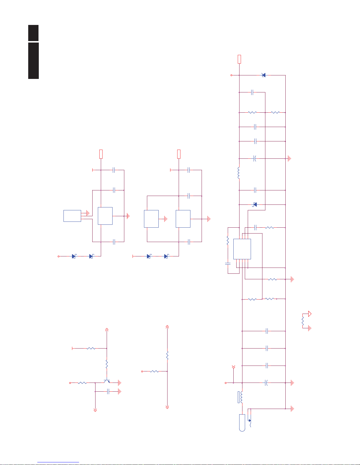
Meridian 2
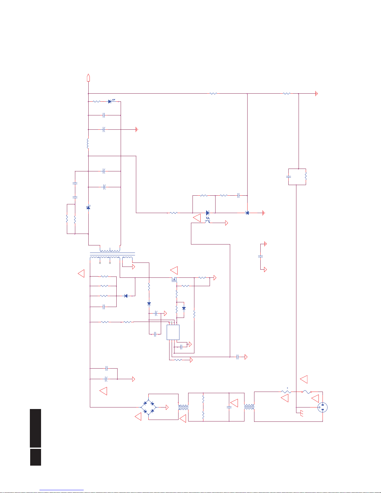
6.2 Adapter Board (715G3980P0D0000030)
Remark: Parts position can be searched by using FIND function in PDF.
1 2
D906
Diode MBR20100CT
R907
560K 1/4W
C930
10N 50V
R942
100OHM +-5% 1/8W
C925
1500PF2KV
R919
45.3KOHM +-1% 1/10W
D902
1N4007
R937
560K 1/4W
LED1
LED
R910
100K 1/8W
R906
10K 1/4W
D903
1N4007
+
C929
47uF/50V
R938
560K 1/4W
C931
100pF50V
!
!
R934
10K 1/4W
+
C927
100uF 25V
!
R922
470OHM +-5% 1/8W
+
C919
680UF 25V
!
!
!
+12V/3A
F901
FUSE
Q901
SMK0965F
R947
4.7 OHM
R9040.47OHM2W
12
3
CN901
SOCKET
2
1
3
4
-
+
BD901
KBP306G-05
R901
1 MOHM +-5% 1/4W
R902
1 MOHM +-5% 1/4W
C903 0.47UF
R940
220 OHM 1/10W
C908
2N2 500V
1
4
2
3
L902
14mH
L903
0.8uH
R918
20K 1/10W 5%
C920
1U 25V
1
4
2
3
L901
0.45mH
!
+
C918
680UF 25V
R941
1R5 1/8W 5%
R916
11.5KOHM +-1% 1/8W
+
C907
82uF 450V
R911
2KOHM 1/10W
R912
1K 1/10W
R905
10K OHM +-5% 1/8W
C910
100N 50V
12
43
IC902
PC123X2YFZOF
IC903
KIA431A-AT/P
C900
0.001uF/250V
!
12
t
NR901
NTCR 5 OHM 3A
!
C915
0.047uF 50V
C909
10NF1KV
R914
100 OHM 1/4W
R903
1M OHM +-5% 1/8W
C901
1U 25V
C911
2N2 500V
!
NC
FL2
6
5
9
FL1
8
4
T901
700uH
LATCH1COMP2CS3GND
4
OUT
5
VCC
6
NC
7
HV
8
IC901
LD7750GS
D908 LL4148
R908
100 OHM 1/4W
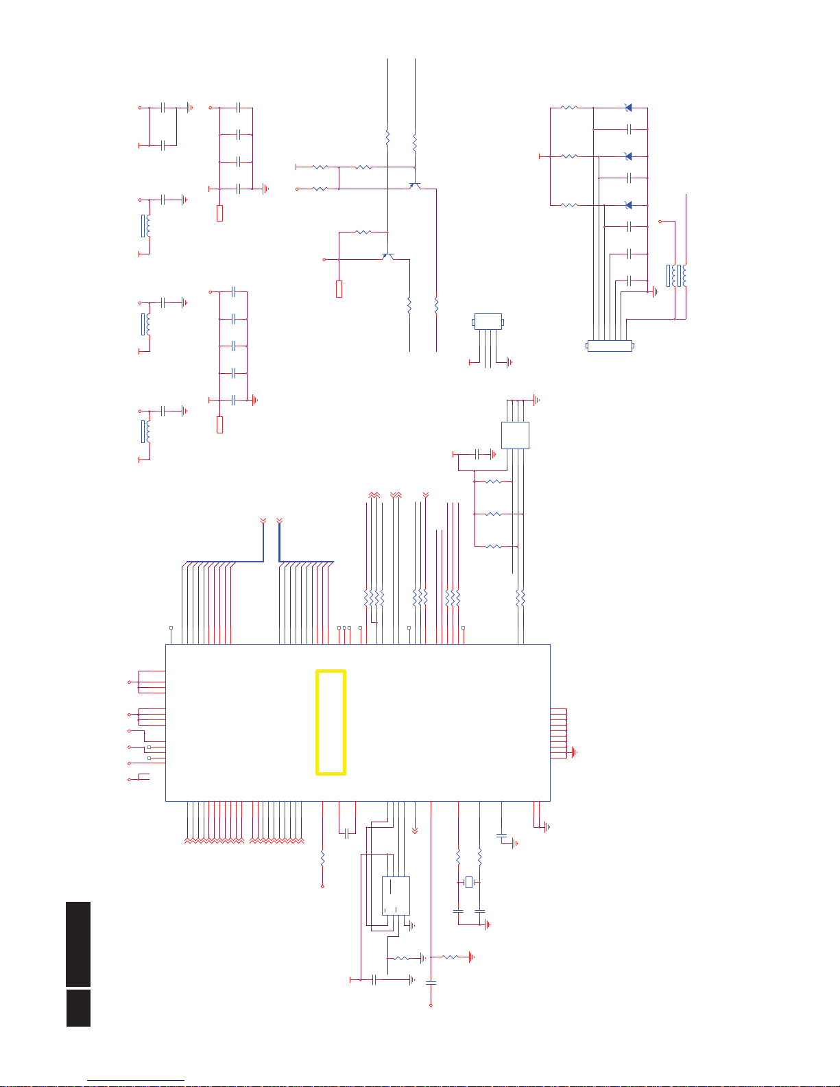
29 Meridian 2
6.3 Inverter Board
191E2 (715G3599P01000001S)
Remark: Parts position can be searched by using FIND function in PDF.
3
1
2
D804
BAV70
D801
1N4148
VSEN
1
SSTCMP
2
CT
3
RT1
4
GNDA
5
PDR2
6
GNDP
7
NDR2
8
NDR19PDR110VDDA11TIMER12PWM13ISEN14OVPT15ENA
16
IC801
ta9687GN-A-0-TR
1
2 CN802
CONN
GND
GND
GND
+12V
+12V
+12V
ENA
DIM
+5V
R807 22 OHM +-1% 1/10W
C807
3.9nF 50V
C810
3.9nF 50V
C813
NC
C818
1N 50V
C816
NC
C804
47N 50V
R803 4R7 1/8W 5%
S11G12S23G2
4
D25D26D17D1
8
Q801
APM4548AKC
R805
5.1K 1/ 8W
1 2
ZD802
BZX79-B5V6
R818
360R 1/ 10W 5%
C805
47N 50V
S11G12S23G2
4
D25D26D17D1
8
Q802
APM4548AKC
R806 4R7 1/8W 5%
R812 4R7 1/8W 5%
R813 4R7 1/8W 5%
C811
2.2U25V
C815
2.2U25V
R821
1M 1/10W 5%
R808
10K 1/10W
1
2 CN803
CONN
R809
10K 1/10W
C803
5pF/3KV
C809
5pF/3KV
C812
33N 50V
R816
91KOHM +-1% 1/8W
OVPT
F801
FUSE
D
G
S
Q803
RK7002FD5T116
+5V
14
2 6
PT801
POWER X'FMR
+5V
C817
33N 50V
14
2 6
PT802
POWER X'FMR
C814
220P 50V
ISEN
R811
1K 1/8W
P1
3
1
2
D802
BAV99
ISEN
R814
560R 1/ 10W 5%
P1
C819
10N 50V
123456789
CN801
CONN
OVPT
+5V
C820
2.2uF 25V
R810
100K 1/10W
R817
100K 1/10W
R820
20K 1/10W
1 2
ZD801
BZX79-B5V6
R804
5.1K 1/ 8W
C
3
B
1
E
2
D803
BAW56
C808 100N 50V
R819
1M 1/10W 1%
+
C806 680uF 16V
R822 0R051/8W
R815
47K 1/4W
!
30
Meridian 2
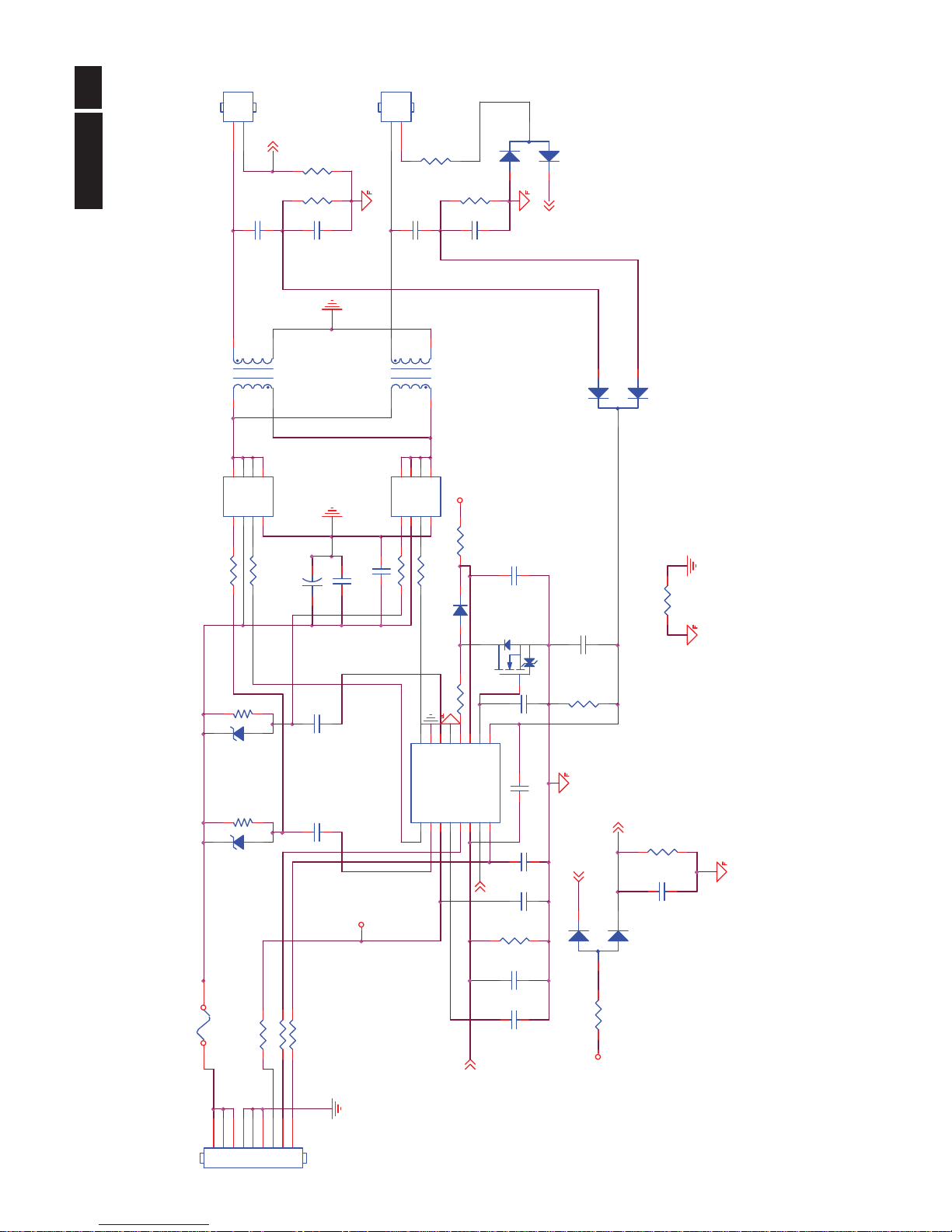
6.4 Converter Board
191EL2 (715G3823P04000004W)
Remark: Parts position can be searched by using FIND function in PDF.
Vout
R817
NC/ 10K 1/10W 5%
R816
NC/ 120KOHM 1/10W
R840 N C / 1 OHM 1/10W
IC801
TA9690GN
123456789
101112 13
1415161718192021222324
PWM
ISEN1
ISEN2
ISEN3
ISEN4
GNDA
ISEN8
ISEN6
ISEN7
OVP
ISET
RT ENA
ISW
ISEN5
LDR
VREF
GNDP
VIN
SEL
COMP
SSTCMP
NC
STATUS
73G253S 80 DN
OVP1
R803
NC/ 1K 1/ 1 0W 5%
OVP2
CN803
NC/CONN
123456789
10
11 12
+
C804
4.7 uF 100V
OVP1
R805
120KOHM 1/10W
R830 N C / 1 OHM 1/10W
R836 N C / 1 OHM 1/10W
R842
56K 1/10W
R820
NC/ 100 OH M 1/10W
R807
0R05 1/10W
C808
NC/ 0.47uF 16V
R818
NC
R814
10 OHM 1/10W
Vout
R841 N C / 1 OHM 1/10W
C805
0.47uF 16V
R829 1 OHM 1/10W
R811
0R05 1/10W
R833 1 OHM 1/10W
F801
FUSE
R827 1 OHM 1/10W
C807
2.2U16V
R802
NC
IC802
NC/TA9690GN
123456789
101112 13
1415161718192021222324
PWM
ISEN1
ISEN2
ISEN3
ISEN4
GNDA
ISEN8
ISEN6
ISEN7
OVP
ISET
RT ENA
ISW
ISEN5
LDR
VREF
GNDP
VIN
SEL
COMP
SSTCMP
NC
STATUS
+
C802
100uF 35V
+14V
ENA
L801
22uH
R835 N C / 1 OHM 1/10W
C806
2U2 25V
R839 N C / 1 OHM 1/10W
C810
100N 50V
R813 10K 1/10W 5%
R812
100 OHM 1/10W
R810
1K 1/10W 5%
ZD801
B360B
R815
NC/ 30K 1/10W
R832 N C / 1 OHM 1/10W
R801
0.15 OHM +-1% 1/4W
C803
100N 50V
R808
NC
CN802
CONN
123456789
10
11 12
R843
NC/ 30K 1/ 10W
R809
100K 1/10W 5 %
R838 NC/1 OHM 1/10W
R804
56K1/10W
R824
43K 1/10W 1%
CN801
CONN
123456789
10
11 12
R844
0 OHM 1/10W
R834 N C / 1 OHM 1/10W
R831 1 OHM 1/10W
R821 NC / 10K 1/ 10W 5%
C809
NC/2.2U16V
R845
NC
R806
10K 1/10W 5%
R823
0 OHM 1/10W
Q801
P8008
123
4 5
678
S2G2S1
G1 D1
D1D2D2
R826 1 OHM 1/10W
R822
1M 1/8W 1%
C816
100N 50V
C801
100N 50V
R825
0R05 1/4W
OVP2
DIM
R837 N C / 1 OHM 1/10W
R819
NC/ 100K 1/ 10W 5 %
R828 1 OHM 1/10W
 Loading...