

Page 1

19” LCD Color Monitor 190P7
1
Service
Service
Service
Horizontal Frequency
30- 83KHz
TABLE OF CONTENTS
Description Page Description Page
SAFETY NOTICE
ANY PERSON ATTEMPTING TO SERVICE THIS CHASSIS MUST FAMILIARIZE HIMSELF WITH THE CHASSIS
AND BE AWARE OF THE NECESSARY SAFETY PRECAUTIONS TO BE USED WHEN SERVICING
ELECTRONIC EQUIPMENT CONTAINING HIGH VOLTAGES.
CAUTION: USE A SEPARATE ISOLATION TRANSFOMER FOR THIS UNIT WHEN SERVICING
Table Of Contents....................................………….1
Revision List........................................…………….2
Important Safety Notice……………..........................3
1. Monitor Specifications……….....................…..4
2. LCD Monitor Description………..…….................5
3. Operation instructions…………….................…....6
3.1 General Instructions……………………………6
3.2 Control buttons……………………………………6
3.3 Adjusting the Picture………….........................…..7
3.4 Connecting to the PC …….............…….……....11
4. Input/Output Specification.......................……….12
4.1 Input Signal Connector..............................…..12
4.2 Factory Preset Display Modes..…........................13
4.3 Pixel Defect Policy…………………………………14
5. Block Diagram…………………………….……...17
5.1 Monitor Exploded View…………….……........17
5.2 Software Flow Chart..............................18
5.3 Electrical Block Diagram..................…….........20
6. Schematic Diagram…...............……….........22
6.1 Main Board…..…..…………………………………22
6.2 Power Board…….………………….…………………27
7. PCB Layout..…….....................……………………..29
7.1 Main Board….................................……………......29
7.2 Power Board……...........................……….............32
7.3 Key Board…….……………………………………35
7.4 USB Board…….………………………………………35
8. Wiring Diagram………………………………………… 36
9. Mechanical Instructions..................…….............37
10.Trouble shooting.…………………………...……48.
11. Repair Flow Chart……….……………………………50
12. ISP Instructions..…..........................………..............55
13. DDC Instructions……......…….....……...............61
14. White Balance, Luminance Adjustment……….......78
15. Recommended& Spare Parts List...………..............79
16. Different Parts List.....................………..............94
17. General Product Specification………………….100
GB 3138 106 10514
190P7ES/00
190P7EB/27
190P7EB/28
190P7EB/00
190P7ES/01
190P7EG/00
190P7EG/01
190P7EB/93
190P7ES/10
190P7EG/10
Page 2
19” LCD Color Monitor 190P7
2
Revision List
Version Release Date Revision History
A00 May.11, 2006 Initial release, Draft Version
A01 Jun.15, 2006
Add CTV Model 190P7EB/00,
190P7EB/27, 190P7EB/28,
190P7EB/93, 190P7EG/00,
190P7EG/01, 190P7ES/01 in Item 16
A02 Aug.22, 2006
Modify product identification and Philips’ Flat
Panel Monitors Pixel Defect Policy
A03 Sep.19, 2006
Make some Engineering Changes
in Item 15 and Item 16
A04 Oct.24, 2006 Add Service Kit in Page 79
A05 Nov.10, 2006 Revise Service Kit in Page 79
A06 Nov.29, 2006 Add DDC Instruction for OSD SN in Item 13
A07 Dec.05, 2006 Add OSD SN Kit in Page 79
A08 Jan.17, 2007 Add To Lock/Unlock OSD function in Page 7
A09 Mar.23, 2007
Add CTV Model 190P7ES/10,
190P7EG/10 in Item 16
A10 Sep.06, 2007 Add To “Recommended parts list ” in Page 79
A11 Nov.12, 2007
Update CTV Model 190P7ES/10,
190P7EG/10 in Item 16
Page 3

19” LCD Color Monitor 190P7
3
Important Safety Notice
Proper service and repair is important to the safe, reliable operation of all Philips Company** Equipment. The
service procedures recommended by Philips and described in this service manual are effective methods of
performing service operations. Some of these service operations require the use of tools specially designed for the
purpose. The special tools should be used when and as recommended.
It is important to note that this manual contains various CAUTIONS and NOTICES which should be carefully read
in order to minimize the risk of personal injury to service personnel. The possibility exists that improper service
methods may damage the equipment. It is also important to understand that these CAUTIONS and NOTICES ARE
NOT EXHAUSTIVE. Philips could not possibly know, evaluate and advise the service trade of all conceivable ways
in which service might be done or of the possible hazardous consequences of each way. Consequently, Philips has
not undertaken any such broad evaluation. Accordingly, a servicer who uses a service procedure or tool which is
not recommended by Philips must first satisfy himself thoroughly that neither his safety nor the safe operation of
the equipment will be jeopardized by the service method selected.
* * Hereafter throughout this manual, Philips Company will be referred to as Philips.
WARNING
Use of substitute replacement parts, which do not have the same, specified safety characteristics may create
shock, fire,
or other hazards.
Under no circumstances should the original design be modified or altered without written permission from Philips.
Philips
assumes no liability, express or implied, arising out of any unauthorized modification of design.
Servicer assumes all liability.
FOR PRODUCTS CONTAINING LASER:
DANGER-Invisible laser radiation when open. AVOID DIRECT EXPOSURE TO BEAM.
CAUTION-Use of controls or adjustments or performance of procedures other than those specified herein may
result in hazardous radiation exposure.
CAUTION -The use of optical instruments with this product will increase eye hazard.
TO ENSURE THE CONTINUED RELIABILITY OF THIS PRODUCT, USE ONLY ORIGINAL MANUFACTURER'S
REPLACEMENT PARTS, WHICH ARE LISTED WITH THEIR PART NUMBERS IN THE PARTS LIST SECTION
OF THIS SERVICE MANUAL.
Take care during handling the LCD module with backlight unit
-Must mount the module using mounting holes arranged in four corners.
-Do not press on the panel, edge of the frame strongly or electric shock as this will result in damage to the screen.
-Do not scratch or press on the panel with any sharp objects, such as pencil or pen as this may result in damage to
the
panel.
-Protect the module from the ESD as it may damage the electronic circuit (C-MOS).
-Make certain that treatment person’s body is grounded through wristband.
-Do not leave the module in high temperature and in areas of high humidity for a long time.
-Avoid contact with water as it may a short circuit within the module.
-If the surface of panel becomes dirty, please wipe it off with a soft material. (Cleaning with a dirty or rough cloth
may damage the panel.)
Page 4
19” LCD Color Monitor 190P7
4
1. Monitor Specifications
LCD Panel
Screen type Active matrix - TFT LCD
Panel Type M190EG01 (AUO)
Size 19.0"
Pixel pitch 0.294mm(H) x 0.294mm(V)
Viewable angle (CR=10) Horizontal 178º, Vertical 178º (type) (AUO)
Response time 8 ms (type)
Separate Sync
TTL level, input impedance 2.2k OHM terminate
Horizontal Frequency 30kHz – 83kHz
Vertical refresh rate 56 - 76Hz
Input Connector
28pin DVI A
28pin DVI B
Maximum Resolution
1280 x 1024 at 75Hz (analog input)
1280 x 1024 at 75Hz (digital input)
Display Colors 16.7M colors (RGB 8-bits data)
Contrast Ratio 1000:1
White Luminance 300cd/m2
Video dot rate 140 MHz
Recommended Resolution 1280 x 1024 at 60Hz (digital input)
Plug & Play VESA DDC2B
Power Consumption
Power on: < 40 W
Power off: < 1 W
Input Video Signal 0.7 Vp-p, input impedance, 75 ohm @DC
Tilt -5° ~ 25°
Maximum Screen Size
Horizontal: 376.32mm;Vertical: 301.056 mm
Power Source
100-240 VAC, 50/60 Hz
Weight 8.2Kg
Environmental
Considerations
Operating Temp: 0°C to 40°C
Storage Temp.: -20°C to 60°C
Relative Humidity: 20% to 80%
Cabinet color Black/Silver/Gray
Page 5
19” LCD Color Monitor 190P7
5
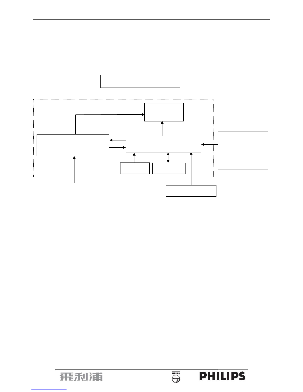
2. LCD Monitor Description
The LCD MONITOR will contain a main board, PWPC board, keypad board and a USB board which house the
flat panel control logic, brightness control logic and DDC.
The power board will provide AC to DC Inverter voltage to drive the backlight of panel and the main board chips
each voltage.
Video signal, DDC
Flat Panel and
CCFL backlight
Keyboard
RS232 Connector
For white balance
adjustment in factory
mode
CCFL Drive.
AC-IN
100-240V
Monitor Block Diagram
HOST Computer
USB Board
Main Board
PWPC board
(Included: adapter and inverter)
Page 6
19” LCD Color Monitor 190P7
6
3. Operation instructions
3.1 General Instructions
Press the power button to turn the monitor on or off. The other control buttons are located at front panel of the
monitor. By changing these settings, the picture can be adjusted to your personal preferences.
-
The power cord should be connected.
-
Connect the video cable from the monitor to the video card.
-
Press the power button to turn on the monitor, the power indicator will light up.
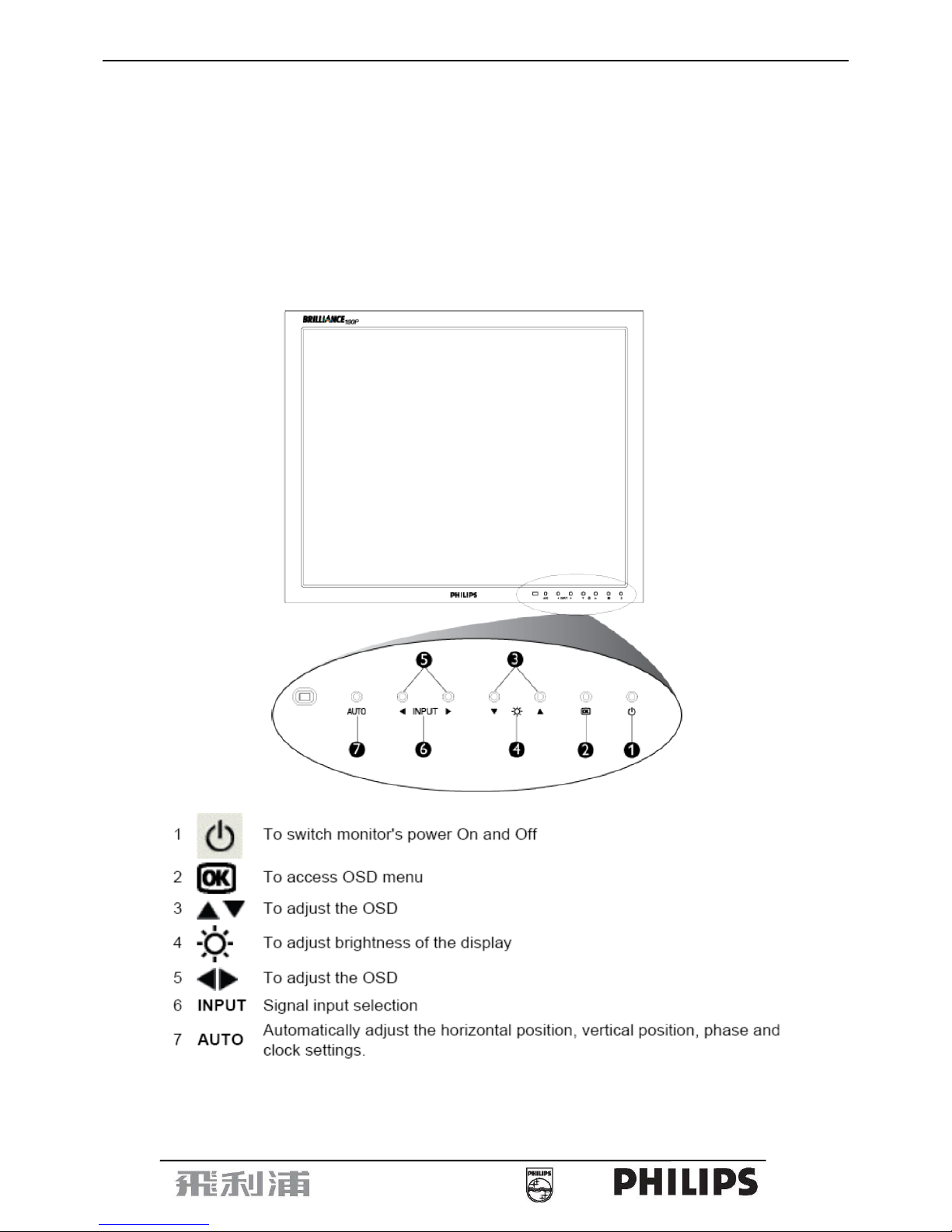
3.2 Control Buttons
Front View
Page 7
19” LCD Color Monitor 190P7
7
Rear View
3.3 Adjusting the Picture
This is a feather in all Philips LCD monitors. It allows an end user to adjust screen performance of the monitors
directly through an on-screen instruction window. The user interface provides user-friendliness and ease-of-use
when operating the monitor.
When you press the
button on the front control of your monitor, the On-Screen Display (OSD) Main Controls
window will pop up and you can then start making adjustments to your monitor’s various features. Use the
or the
keys to make your adjustments.
To Lock/Unlock OSD function (User Mode)
The OSD function can be locked by pressing “MENU” button for more than 10 seconds.
Locked OSD function can be released by pressing “MENU” button for more than 10 seconds again.
Page 8
19” LCD Color Monitor 190P7
8
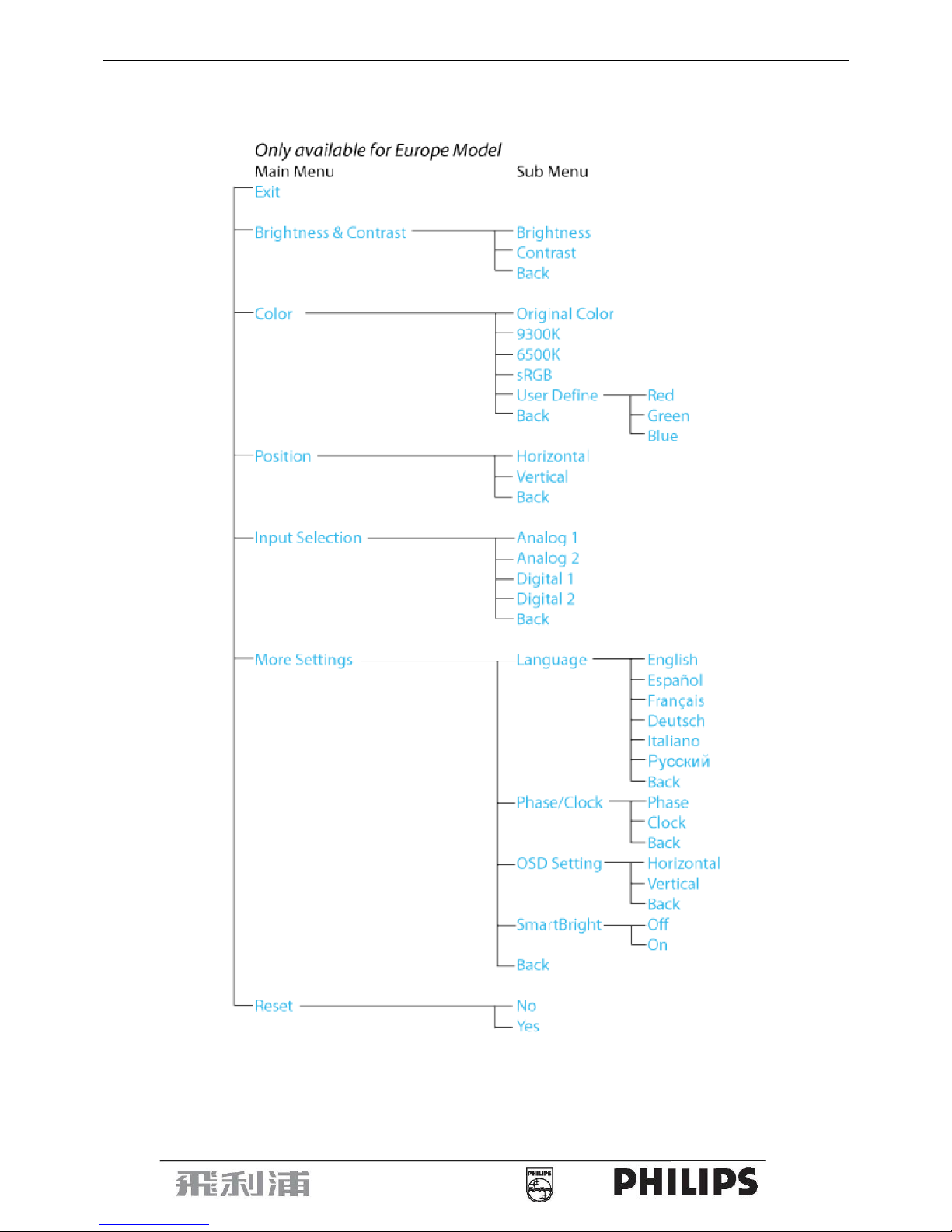
The OSD tree
Below is an overall view of the structure of the On-Screen Display. You can use this as a reference when you want to
work your way around the different adjustments later on.
Page 9

19” LCD Color Monitor 190P7
9
Page 10

19” LCD Color Monitor 190P7
10
Page 11
19” LCD Color Monitor 190P7
11
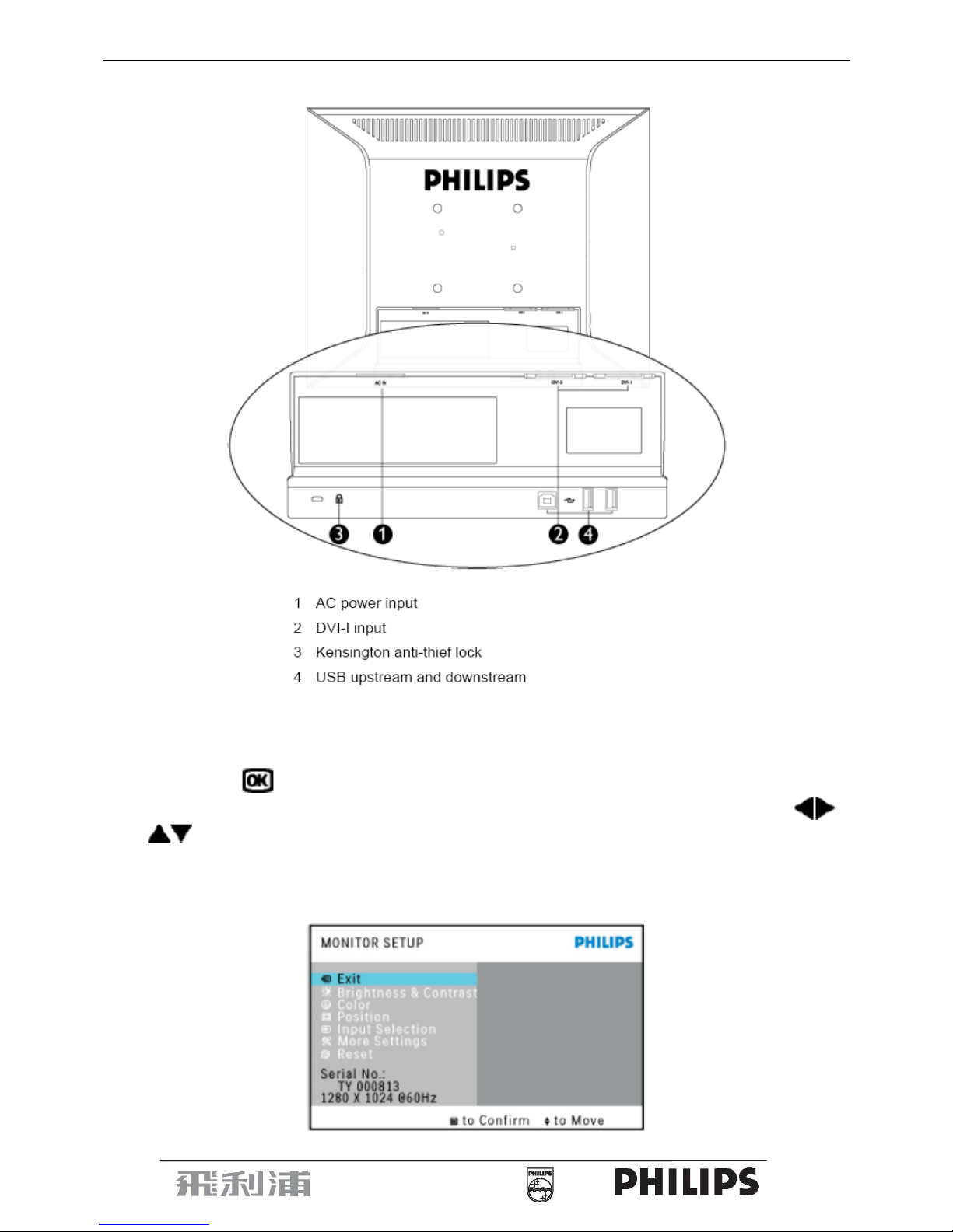
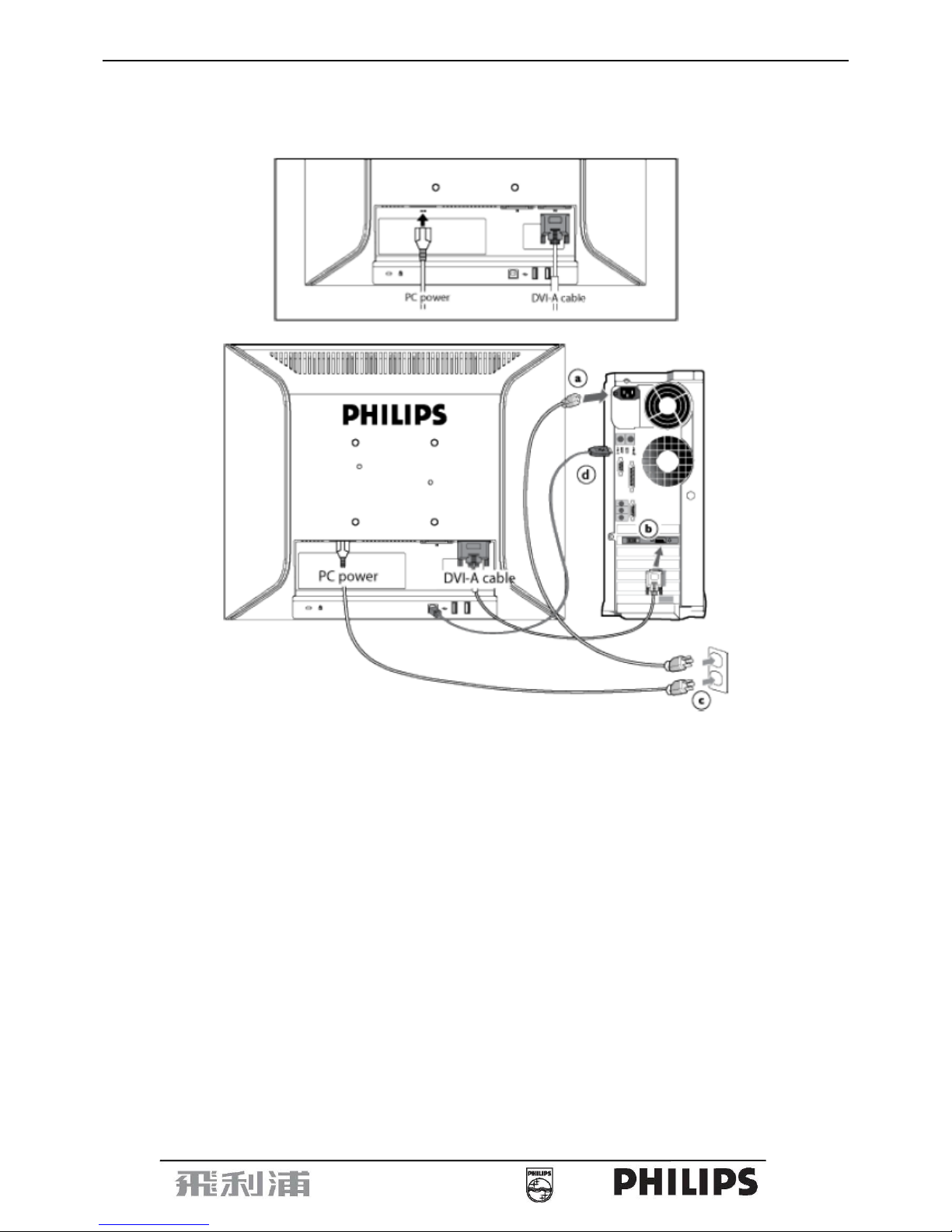
3.4 Connecting to the PC
1) Connect the power and DVI cable to the back of the monitor firmly. (Philips has pre-connected DVI-A cable for the
first installation.)
2) Connect the cables to the back of your computer by following theses steps:
(a) Turn off your computer and unplug its power cable.
(b) Connect the monitor signal cable to the video connector on the back of your computer.
(c) Plug the power cord on your computer and your monitor into a nearby outlet.
(d) USB plug
(1) Connect USB upstream port on monitor and the USB port on PC with a USB cable.
(2) The USB downstream port is now ready for any USB device to plug in.
(e) Turn on your computer and monitor. If the monitor displays an image, installation is complete.
Note: The USB plug is a pass through connection whether it can support USB 1.1 or USB 2.0 depends on
your PC’s specification.
Page 12
19” LCD Color Monitor 190P7
12
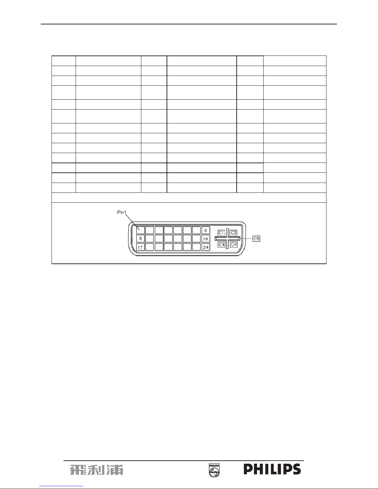
4. Input/Output Specification
4.1 Input Signal Connector
DVI A/B connectors
Pin No. Description Pin No. Description Pin No.
Description
1.
T.M.D.S Data 2-
13. NC C1 * Analog R
2.
T.M.D.S Data 2+
14.
+5V Power
C2 * Analog G
3. T.M.D.S Data 2 Shield 15.
GND (return for + 5V and
H/V-sync)
C3 * Analog B
4. NC 16. Hot Plug Detect C4 * Analog H-sync
5. NC 17.
T.M.D.S Data 0-
C5
* Analog GND
(Analog R, G, B return)
6. DDC Clock 18.
T.M.D.S Data 0+
7. DDC Data 19. T.M.D.S Data 0
8. Analog V-sync 20. NC
9.
T.M.D.S Data 1-
21. NC
10.
T.M.D.S Data 1+
22. T.M.D.S Clock Shield
11. T.M.D.S Data 1 Shield 23. T.M.D.S Clock +
12. NC 24.
T.M.D.S Clock -
DVI Connector layout
Page 13
19” LCD Color Monitor 190P7
13
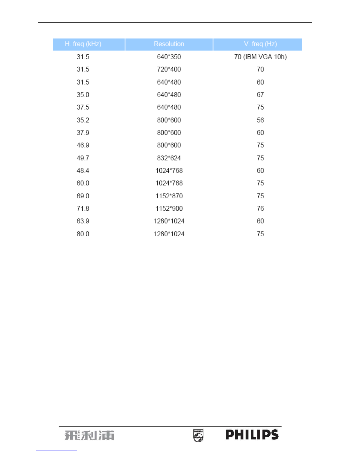
4.2 Factory Preset Display Modes
Page 14
19” LCD Color Monitor 190P7
14
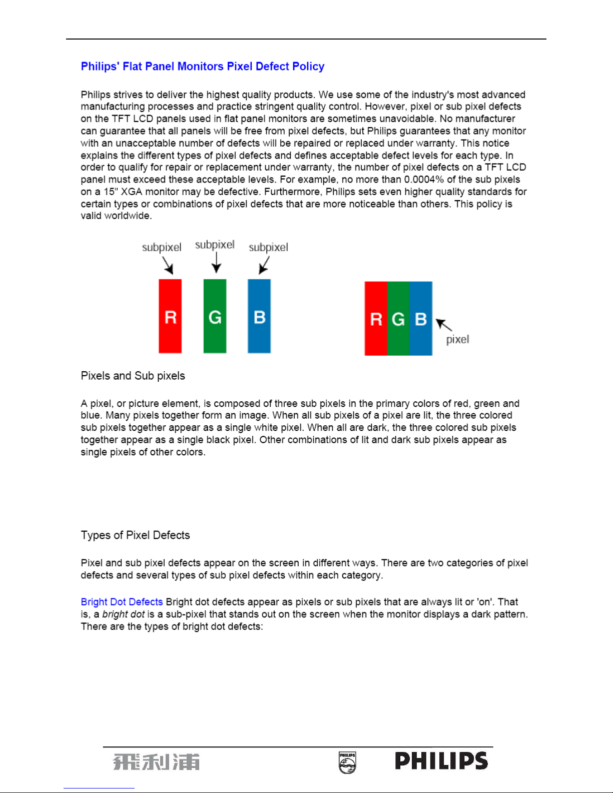
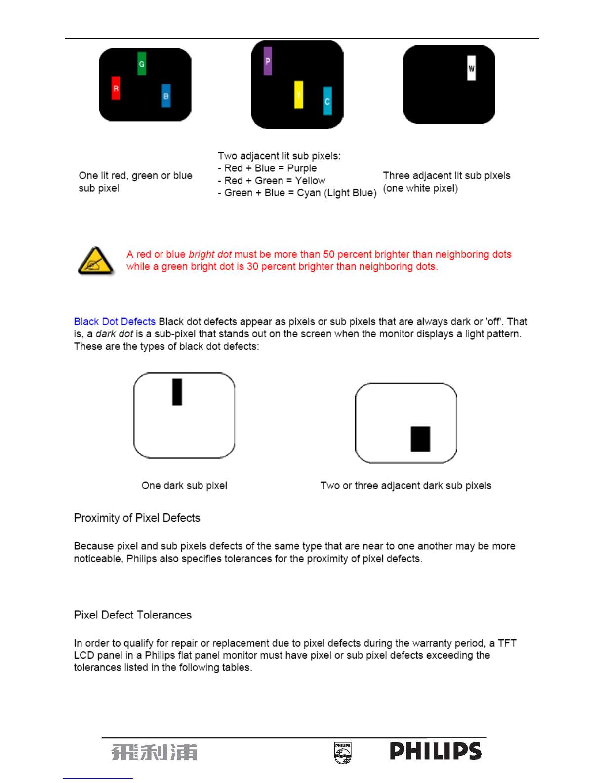
4.3 Pixel Defect Policy
Page 15
19” LCD Color Monitor 190P7
15
Page 16

19” LCD Color Monitor 190P7
16
Page 17
19” LCD Color Monitor 190P7
17
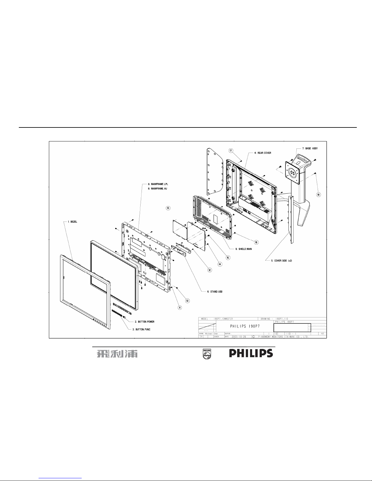
5. Block Diagram
5.1 Monitor Exploded View
Page 18
19” LCD Color Monitor 190P7
18
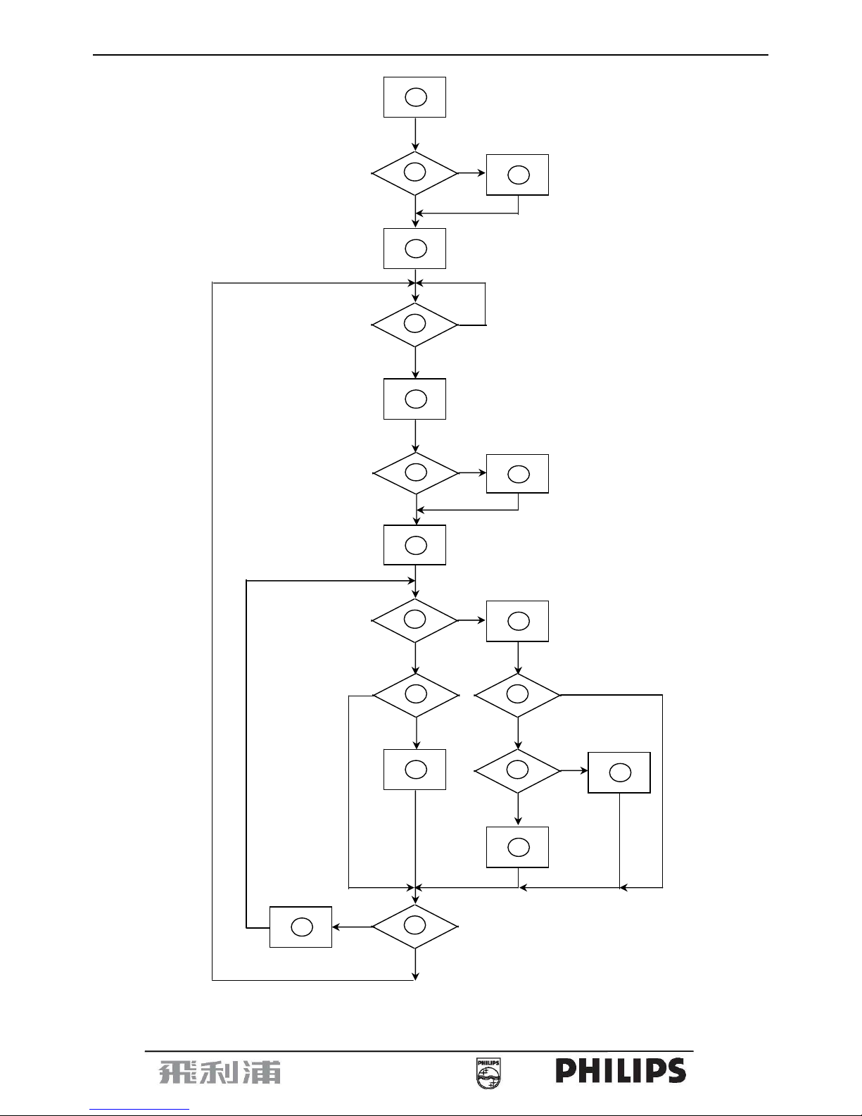
5.2 Software Flow Chart
1
2
N
Y
5
Y
N
10
Y
N
12
Y
N
7
Y
N
6
4
3
8
9
14
11
13
Y
N
15
Y
N
16
17
19
Y
N
18
Page 19

19” LCD Color Monitor 190P7
19
1) MCU Initializes.
2) Is the EEprom blank?
3) Program the EEprom by default values.
4) Get the PWM value of brightness from EEprom.
5) Is the power key pressed?
6) Clear all global flags.
7) Are the AUTO and SELECT keys pressed?
8) Enter factory mode.
9) Save the power key status into EEprom.
Turn on the LED and set it to green color. Scalar initializes.
10) In standby mode?
11) Update the lifetime of back light.
12) Check the analog port, are there any signals coming?
13) Does the scalar send out an interrupt request?
14) Wake up the scalar.
15) Are there any signals coming from analog port?
16) Display "No connection Check Signal Cable" message. And go into standby mode after the message
disappears.
17) Program the scalar to be able to show the coming mode.
18) Process the OSD display.
19) Read the keyboard. Is the power key pressed?
Page 20
19” LCD Color Monitor 190P7
20
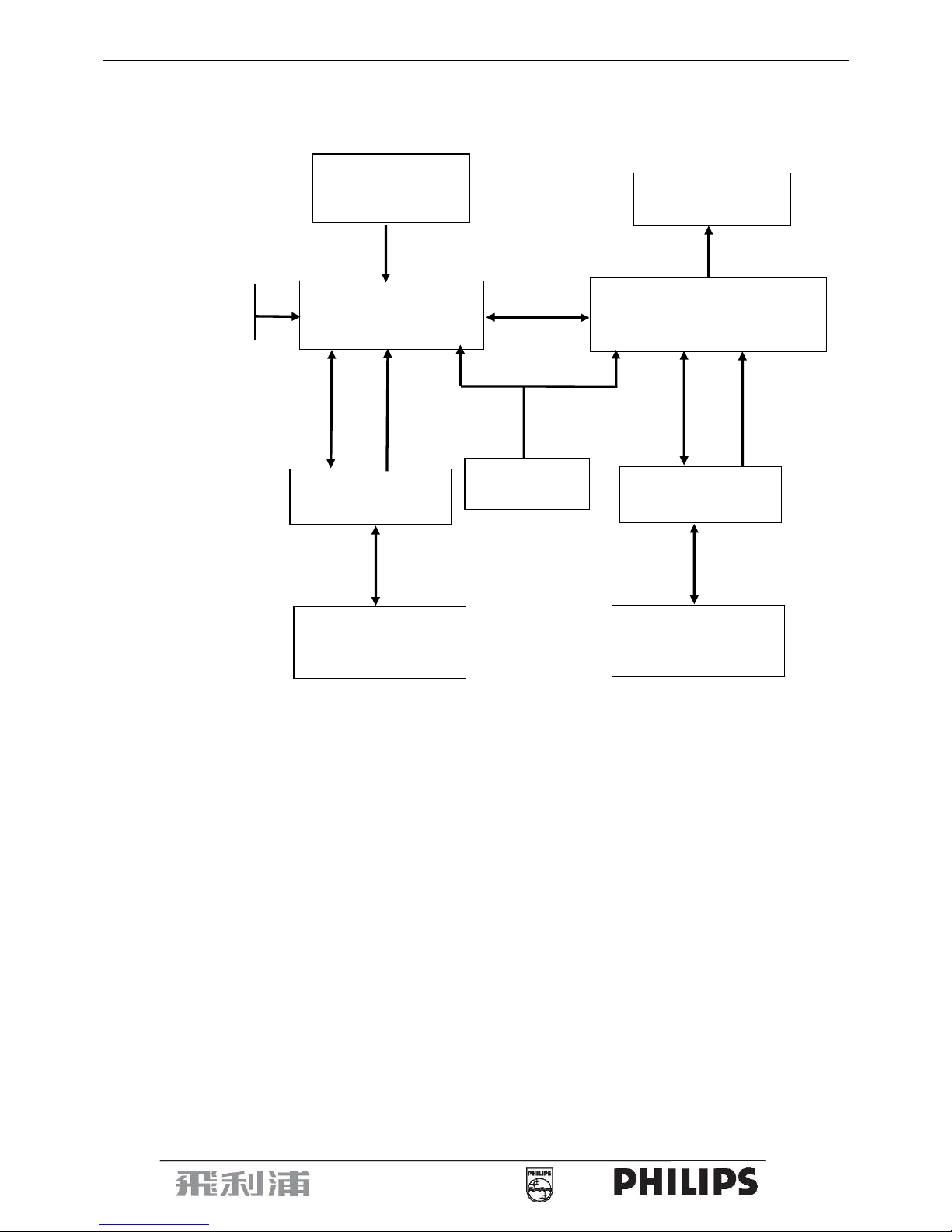
5.3 Electrical Block Diagram
5.3.1 Main Board
Panel Interface
(CN501)
NT68563EFG
(Include Scalar B, ADC, OSD)
(U401)
DVI B Connector
(CN201)
EEPROM
BU9882FV-W
(U201)
-
B-HS
B-VS
B_SDA
B_SCL
NT68663MEFG
(Include MCU, Scalar A)
(U301)
Crystal 12MHz
(
X301
)
EEPROM
M24C16-WMN6TP
(
U303
)
Keypad Interface
(CN503)
DVI A Connector
(CN101)
EEPROM
BU9882FV-W
(U101)
A_SDA
A_SCL
-
A-HS
A-VS
Page 21
19” LCD Color Monitor 190P7
21
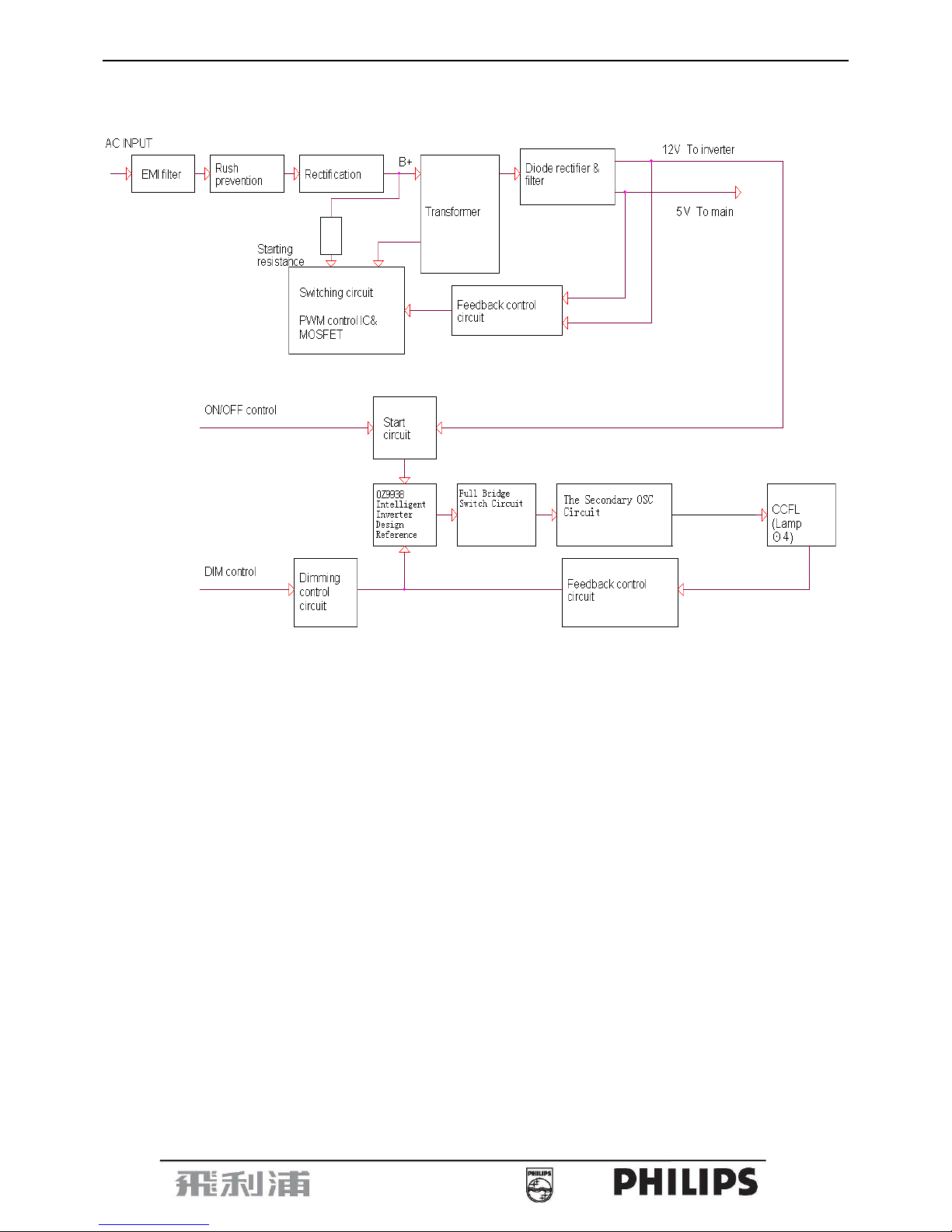
5.3.2 Inverter/Power Board
Page 22
19” LCD Color Monitor 190P7
22
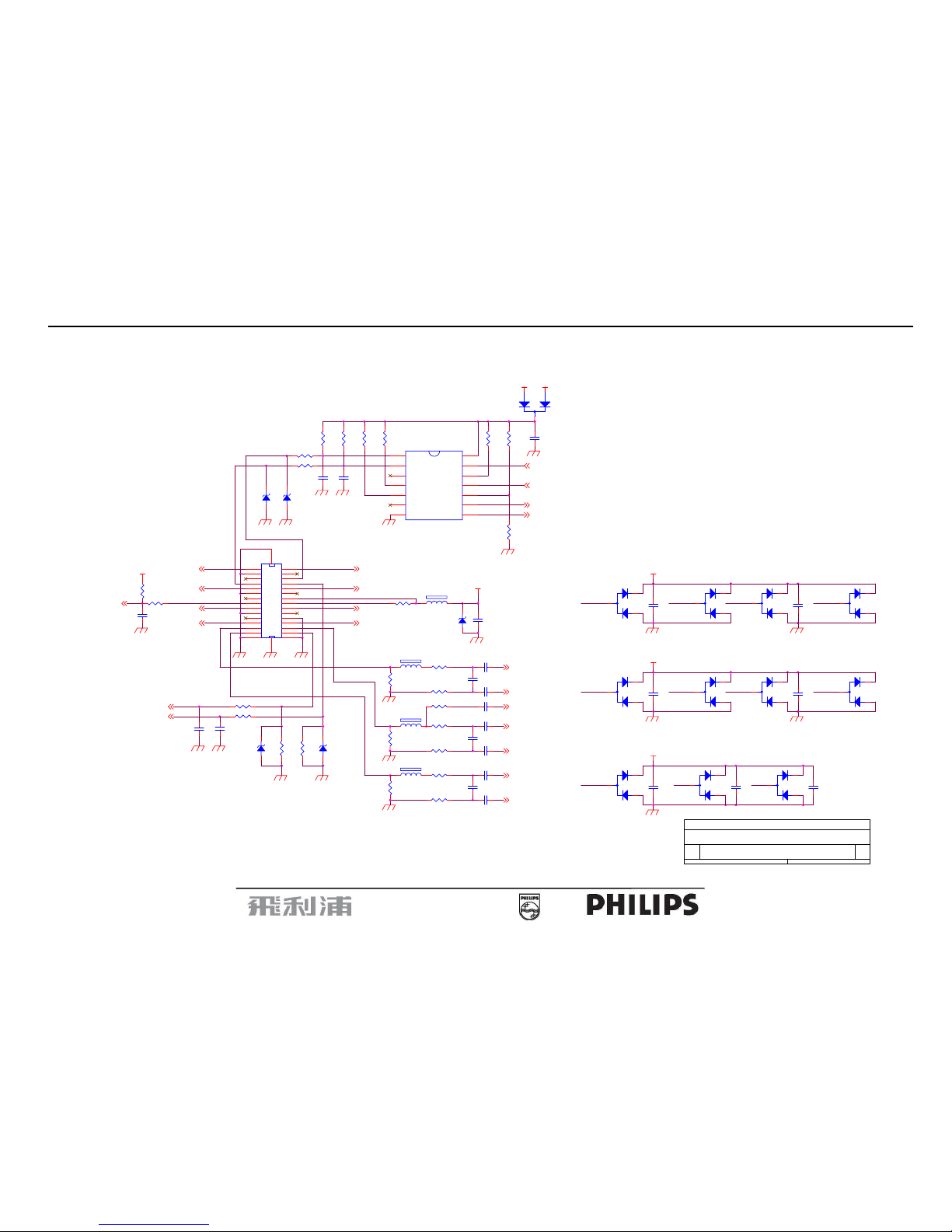
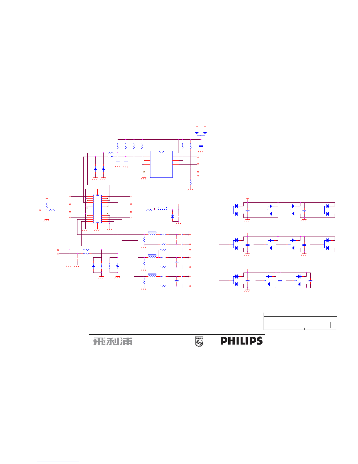
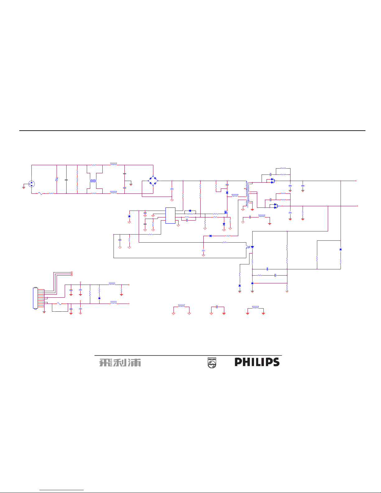
6. Schematic Diagram
6.1 Main Board
715G1791- 1
DVI INPUT A
1
190P7 Schematic
A3
15Sunday, January 08, 2006
Title
Size Document Number Rev
Date: Sheet
of
A_RX1+ 3
C113
0.047uF
R101
10K
R111
75
ZD103
BZX84-C5V1
1 3
A_RXC- 3
A_B
R125
10K
A_RX1-3
R120
2.2K
C120
NC
C118
33pF
A_GNDR 3
A_RX2-
R113
150
A_RXC+
A_RX0+
A_HS3
+3.3VCC
C102
0.1uF
A_RXC+3
ZD105
BZX84-C5V1
1 3
D105
BAV99 (NC)
3
1
2
A_R
R119
2.2K
D110
BAV99 (NC)
3
1
2
A_RX2-3
C123
NC
A_GIN 3
C112
0.1uF (NC)
C124
0.047uF
R107 100
D102
BAV99 (NC)
3
1
2
C122
0.047uF
A_RXC+
FB102
30 OHM
1 2
C101
0.1uF (NC)
A_SDA 3
R117
75
R126
10K (NC)
A_DVI_5V
A_CABLE3
A_RX0-3
ZD104
BZX84-C5V1
1 3
R102
10K
R121
150
A_G
+3.3VCC
R124
150
U101
BU9882FV-W
1
2
3
4
5
6
7
14
13
8
9
10
11
12
SCL_PC0
SDA_PC0
NC
SCL_PC1
SDA_PC1
NC
GND
VCC
WPB
SDA_MON
SCL_MON
DDCENA
BANKSEL
DUALPCB
A_RX0+
R112
75 1%
C111
0.1uF (NC)
D107
BAV99 (NC)
3
1
2
A_VS3
A_SOG 3
C116 0.047uF
A_DVI_5V
D106
BAV99 (NC)
3
1
2
C119
220pF
R115
390
A_RX1-
A_RXC-
FB104
30 OHM
1 2
A_RX0-
R114 100
A_RIN 3
A_BIN 3
R122
75
C106
0.1uF (NC)
R116 100
D104
BAV99 (NC)
3
1
2
R106
10K
CN101
DVI #A
2
4
6
8
10
12
14
16
18
20
22
24
26
28
1
3
5
7
9
11
13
15
17
19
21
23
25
27
29 30
31 32
R103
10K (NC)
A_RX1+
FB103
30 OHM
1 2
C103
0.1uF (NC)
+3.3VCC
C104
330pF
C107
0.1uF (NC)
C109
0.1uF
ZD101
BZX84-C5V1
1 3
A_RX0-
D111
BAV99 (NC)
3
1
2
C108
0.1uF
R123
75 1%
+5V
A_RX2+
R110 1K
C110
0.1uF (NC)
A_RX2+ 3
A_GNDG 3
C105
330pF
D108
BAV99 (NC)
3
1
2
FB101
120 OHM
R108 100
R105
10K
D112
BAV99 (NC)
3
1
2
C117 0.047uF
A_RXC-
C121
0.047uF
D101
BAV70
A_GNDB 3
A_DDC_SEL 3
C115
0.047uF
A_R
A_RX2+
R118
75 1%
A_DDC_WP 3
+3.3VCC
A_RX1+
A_RX2-
R104
10K
D103
BAV99 (NC)
3
1
2
A_SCL 3
A_RX1-
R109
1K
A_B
D109
BAV99 (NC)
3
1
2C114
NC
ZD102
BZX84-C5V1
1 3
A_G
A_RX0+ 3
Page 23
19” LCD Color Monitor 190P7
23
B_DVI_5V
B_RX0-4
B_RX1+
D206
BAV99 (NC)
3
1
2
B_BIN 4
B_SDA 3
B_CABLE3
B_G
R218
75 1%
C206
330pF
D205
BAV99 (NC)
3
1
2
B_RX1-4
R226
10K (NC)
CN201
DVI #B
2
4
6
8
10
12
14
16
18
20
22
24
26
28
1
3
5
7
9
11
13
15
17
19
21
23
25
27
29 30
31 32
B_RXC- 4
B_RXC-
C208
0.1uF
ZD204
BZX84-C5V1
1 3
B_RXC+
C222
0.047uF
R203
10K (NC)
B_VS4
R212
75 1%
B_RIN 4
B_RX2-4
B_B
R225
10K
B_RX0-
B_RX1-
FB201
120 OHM
B_DDC_WP 3
R221
150
R213
150
C214
NC
B_RX1+ 4
ZD202
BZX84-C5V1
1 3
C205
330pF
R215
390
C219
220pF
C218
33pF
ZD203
BZX84-C5V1
1 3
B_SOG 4
B_RX0+
B_RX0+ 4
R223
75 1%
B_RXC+4
B_RX2-
R220
2.2K
R206
10K
FB202
30 OHM
1 2
R205
10K
C211
0.1uF (NC)
R217
75
R201 100
ZD205
BZX84-C5V1
1 3
B_GNDG 4
B_RX2+
C209
0.1uF
DVI INPUT B
1
190P7 Schematic
A3
25Sunday, January 08, 2006
Title
Size Document Number Rev
Date: Sheet
of
C212
0.1uF (NC)
D202
BAV99 (NC)
3
1
2
B_DVI_5V
R222
75
B_B
+5V
R209
1K
B_RXC-
C221
0.047uF
U201
BU9882FV-W
1
2
3
4
5
6
7
14
13
8
9
10
11
12
SCL_PC0
SDA_PC0
NC
SCL_PC1
SDA_PC1
NC
GND
VCC
WPB
SDA_MON
SCL_MON
DDCENA
BANKSEL
DUALPCB
B_RX2-
C215
0.047uF
B_RX0-
+3.3VCC
+3.3VCC
R216 100
C216 0.047uF
C224
0.047uF
B_HS4
B_RXC+
R210 1K
B_RX2+ 4
B_RX1-
C213
0.047uF
C207
0.1uF (NC)
C204
0.1uF (NC)
C217 0.047uF
R224
150
+3.3VCC
D212
BAV99 (NC)
3
1
2
R211
75
B_GIN 4
D207
BAV99 (NC)
3
1
2
R207
10K
D201
BAV70
C201
0.1uF (NC)
D204
BAV99 (NC)
3
1
2
R202
10K
C220
NC
B_RX2+
B_RX0+
FB203
30 OHM
1 2
C203
0.1uF (NC)
D203
BAV99 (NC)
3
1
2
B_GNDB 4
B_SCL 3
D209
BAV99 (NC)
3
1
2
+3.3VCC
C223
NC
FB204
30 OHM
1 2
D208
BAV99 (NC)
3
1
2
B_DDC_SEL 3
B_G
B_R
C210
0.1uF (NC)
R214 100
C202
0.1uF
D211
BAV99 (NC)
3
1
2
D210
BAV99 (NC)
3
1
2
R219
2.2K
ZD201
BZX84-C5V1
1 3
B_GNDR 4
R204
10K
B_RX1+
R208 100
B_R
Page 24
19” LCD Color Monitor 190P7
24
MCU_VDD
X301
12MHz
R322
100
A_GNDR1
VSO_A
R313
NC
TO DEBUG
ADC_VAA
R333
4.7K
C312
0.1uF
A_AVCC
A_SDA 1
SMART_BRI 5
IICSCL
C314
0.1uF (NC)
TXE3- 4,5
A_RIN1
R305
100 (NC)
MCU_VDD
IICSDA
C319
NC
U303
M24C16
1
2
3
4 5
6
7
8
NC
NC
NC
VSS SDA
SCL
WC
VCC
A_VS1
R306
10K
TXO3- 4,5
PANEL_PWR 5
A_SOG1
IICSCL 4
99
RSTN_B 4
+3.3VCC
TXE0- 4,5
C324
22pF
R307
4.7K
R320
1M
R312
100
C302
0.1uF
OSD 5
A_DDC_SEL 1
A_RX0+1
BRIGHTNESS
4,5
24C16_WP
112
A_AVCC
B_SDA 2
IRQN_B 4
VSO_A
R309
4.7K
C322
0.1uF
A_AVCC
OSC 4
HSO_A
R329
100 (NC)
+
C326
470UF/16V
KEY 5
TO RS232
LED_G 5
TXEC- 4,5
A_GNDB1
C308
0.1uF
TXOC+ 4,5
IICSCL
C317
0.1uF
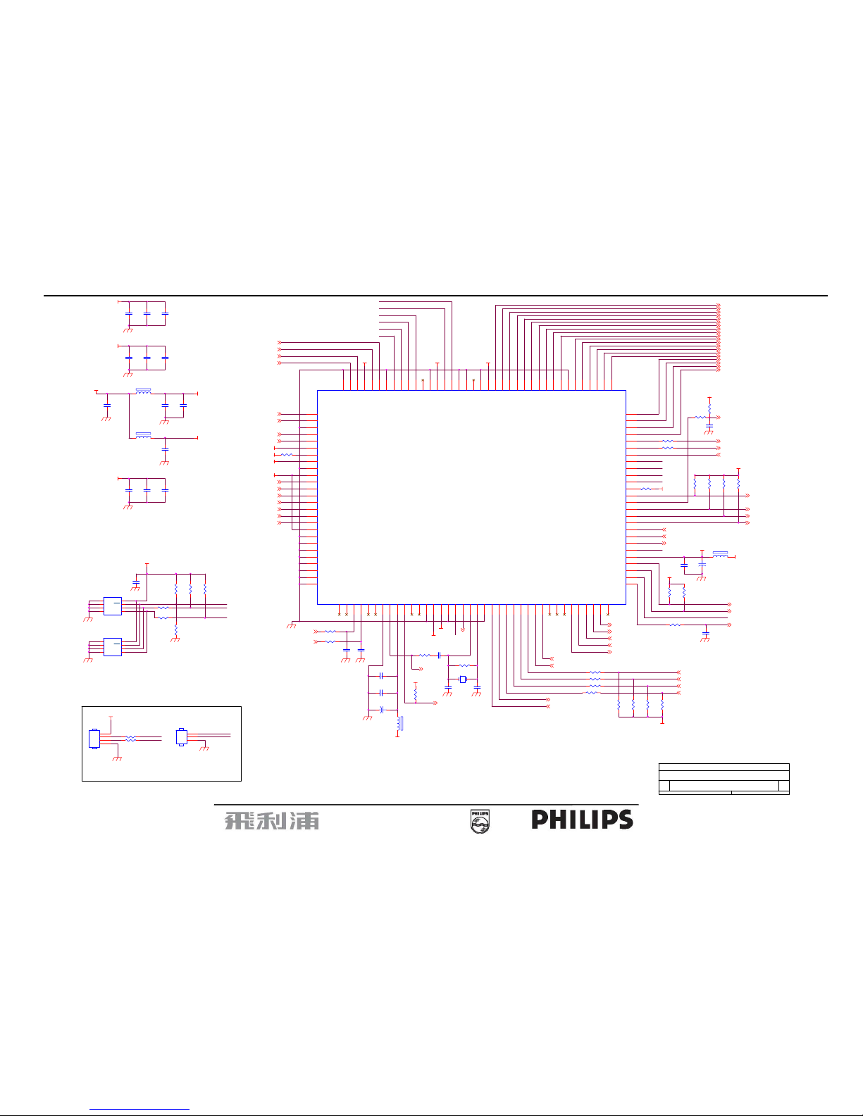
U301
NT68663MEFG-128
39
46
47
50
51
52
53
54
40
48
49
171819202122232425262728293031323334353637
38
678911
12
55
56
57
58
59
60
69707172737674
777879808182838485
86
96
97
111
12345
1013141615
41
42
43
44
45
61
62
63
64
656667
68
75
878889909192939495
9899100
101
103
102
104
110
109
108
107
106
105
117
116
115
114
113
112
118
119
120
121
122
124
123
126
125
128
127
PC3/PWM0
PA1/PWM3
PA2/PWM4
PA5/PWM7*
PA6/PWM8*
PA7/PWM9*
RSTB
P30/RXD
PC2
PA3/PWM5
PA4/PWM6*
PE0
PE1
OSCO
OSCI
MCU_GND
PB0/ADC0
PB1/ADC1
PB4/DDC_SCL0*
PB5/DDC_SDA0*
PB6/DDC_SCL1*
PB7/DDC_SDA1*
PD5
PD4
PD3NCNC
PD2
PD1
PC7
PC6
PC5
PC4/PWM1
VSYNCI0
DPLL_GND
TCLK
DPLL_VDD
PWM11
TS_CLK
PD6
P31/TXD
PB2/ADC2/INTE0
PB3/ADC3/INTE1
P34/T0
P35/T1
T4P
T4M
DGND
T3P
T3M
T2P
TCLK1P
T2M
T1P
T1M
T0P
T0M
DVDD
DGND
GPO1
GPO2/AD0
GPO3/AD1
AGND
RX2+
PGND
TEST
VREF
HSYNCI1
TOUTP/VSYNCI1
HYNCI0
PWM10
CGND
CVDD
DGND
DVDD
PC1*
PC0*
MCU_VCC
PD0
PA0/PWM2
T7P
T7M
TCLK2P
TCLK2M
T6P
T6M
T5P
T5M
TCLK1M
INT_VSO/GPO4
INT_HSO/GPO5
CVDD
CGND
GPO6
SCL
SDA
RSTN
IRQN
RX2-
AVCC
RX1+
RX1-
RX0+
AGND
RX0-
PVCC
REXT
AVCC
RXC-
RXC+
AGND
GIN1-
GIN1+
SOGI1
BIN1-
BIN1+
ADC_VAA
RIN1+
RIN1-
ADC_VAA
ADC_GNDA
BIN0+
SOGI0
BIN0-
GIN0-
GIN0+
RIN0-
RIN0+
R330
10K (NC)
RX
C323
22pF
BL_CONTROL 5
A_RX2-1
C320
NC
120
NT68663 (MCU+SCALER A)
1
190P7 Schematic
C
35Sunday, January 08, 2006
Title
Size Document Number Rev
Date: Sheet
of
C315
0.1uF
+3.3VCC
+
C316
10UF/50V
TXO0+ 4,5
MCU_VDD
TXO1+ 4,5
IICSDA
C305
0.1uF
R321
100
+3.3VCC
DIP TYPE
A_PVCC
K_PWR 5
108
RX
R325
4.7K
A_RX2+1
DVDD
AUDIO_STANDBY 5
RSTN_A
R327
4.7K
FB303
120 OHM
C321
22pF
PANEL_IDX 5
A_CABLE 1
C318
0.1uF
C306
0.1uF
14
R326
4.7K
CVDD18
A_PVCC
A_AVCC
R311
100
HSO_A
R318
22
24C16_WP
TXO2+ 4,5
R302
100
C311
10uF
TXO2- 4,5
A_GNDG1
B_DDC_SEL 2
R308
4.7K
A_RXC-1
TX
C310
0.1uF
TXE2+ 4,5
IRQN_A
R301
100
C304
10uF
CN302
CONN (NC)
1
2
3
82
A_SCL 1
MCU_VDD
A_RX0-1
TX
R310
4.7K
MCU_VDD
TXE1- 4,5
IICSDA
R304
100
R316
100
SMT TYPE
MCU_VDD
R324
4.7K
R303
390
R331
4.7K
TXE1+ 4,5
A_GIN1
VSO_B 4
+1.8VCC
FB301
120 OHM
U302
M24C16-WBN6P (NC)
1
2
3
4 5
6
7
8
NC
NC
NC
VSS SDA
SCL
WC
VCC
DVDD
LED_R 5
IICSCL
TXE2- 4,5
TXO3+ 4,5
B_CABLE 2
RSTN_A
IICSCL
C325
10uF
C307
0.1uF
FB302
120 OHM
15
R317
100
FB304
1000 OHM
12
AUTO 5
A_RX1+1
C303
0.1uF
CN301
CONN (NC)
1
2
3
4
VOLUME 5
A_BIN1
R319
100
+3.3VCC
TXOC- 4,5
IICSDA
C309
10uF
R332
4.7K
89
IICSDA 4
R315
100
MCU_VDD
R328
100 (NC)
C313
0.1uF
110
TXO0- 4,5
A_RXC+1
B_DDC_WP 2
R314
10K
A_RX1-1
TXE0+ 4,5
A_DDC_WP 1
A_HS1
TXE3+ 4,5
TXO1- 4,5
CVDD18
CVDD18
TXEC+ 4,5
HSO_B 4
DVDD
IRQN_A
C301
10uF
R323
4.7K
ADC_VAA
B_SCL 2
R334
4.7K
Page 25
19” LCD Color Monitor 190P7
25
CVDD18
TXE0+ 3,5
TXE3+ 3,5
DVDD
C410
0.1uF
FB402
120 OHM
72
B_GNDR2
R402 100
C422
0.1uF
18
ADC_VAA
B_PVCC
TXO0+ 3,5
TXO1- 3,5
R401
390
4
B_AVCC
TXOC+ 3,5
C407
0.1uF
B_RXC+2
R403 100
IICSDA3
28
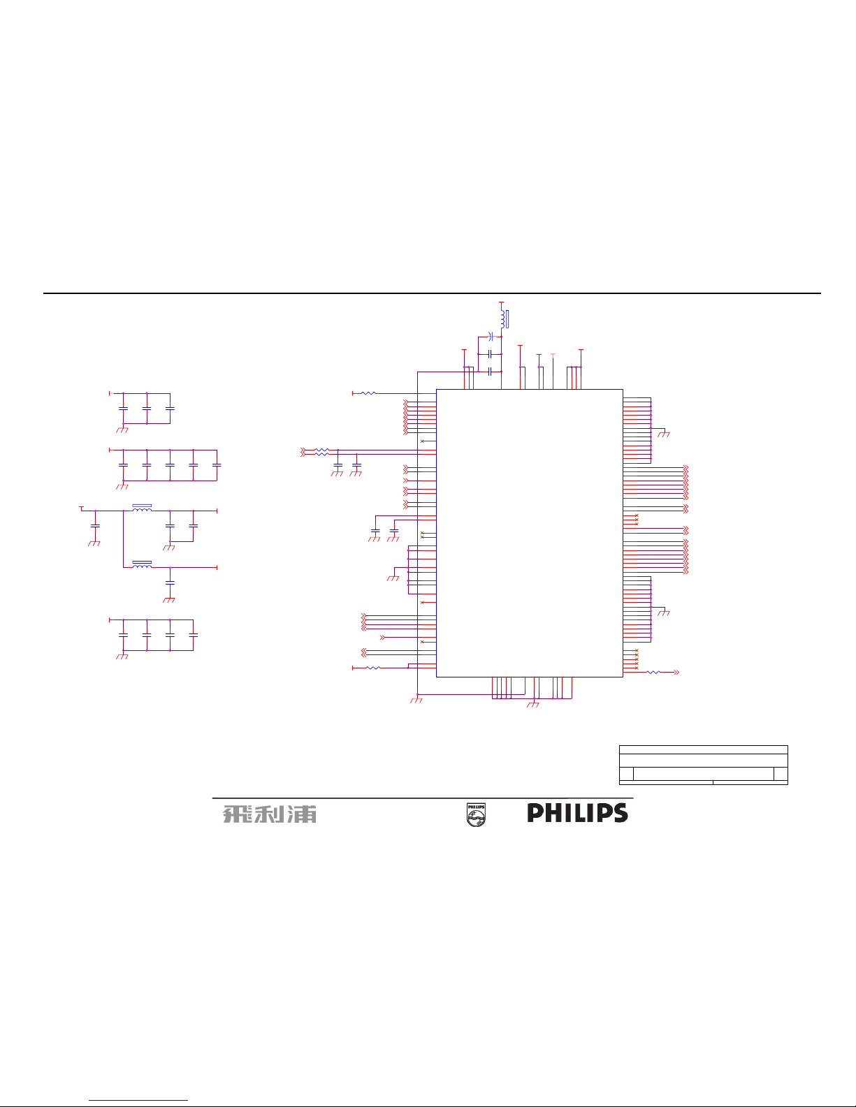
NT68563 (SCALER B)
1
190P7 Schematic
A3
45Sunday, January 08, 2006
Title
Size Document Number Rev
Date: Sheet
of
VSO_B3
TXO2- 3,5
C413
NC
13
TXOC- 3,5
TXE2+ 3,5
+3.3VCC
B_RX1+2
C421
0.1uF
DVDD
C411
0.1uF
B_RX0-2
B_HS2
C406
10uF
TXEC+ 3,5
86
DVDD
C405
0.1uF
C418
0.1uF
TXE2- 3,5
C408
NC
122
TXO2+ 3,5
C409
0.1uF
B_BIN2
B_GIN2
TXEC- 3,5
B_AVCC
IRQN_B3
TXO1+ 3,5
C403
0.1uF
B_AVCC
C404
10uF
B_RXC-2
C415
0.1uF
C402
10uF
ADC_VAA
R404
10K
+1.8VCC
98
B_SOG2
TXE1+ 3,5
C414
10uF
C416
0.1uF
TXE3- 3,5
B_VS2
C417
0.1uF
U401
NT68563EFG
1
2
3
4
5
6
7
8
9
10
11
12
131415
16
17
18
19
20
21
22
23
24
25
26
27
28
29
30
31
32
33
34
35
36
37
38
39
40
41
42
43
44
45
46
47
48
49
50
51
52
53
54
55
56
57
58
59
60
61
62
63
64
102
101
100
99
98
97
96
95
94
93
92
91
90
89
88
87
86
85
84
83
82
81
80
79
78
77
76
75
74
73
72
71
70
69
68
67
66
65
128
127
126
125
124
123
122
121
120
119
118
117
116
115
114
113
112
111
110
109
108
107
106
105
104
103
AGND
RX2+
RX2-
AVCC
RX1+
RX1-
AGND
RX0+
RX0-
AGND
RXC+
RXC-
AVCC
REXT
PVCC
PGND
ADC_GNDA
ADC_VAA
BVMID
BIN1+
BIN1-
SOGI1
GIN1+
GIN1-
RIN1+
RIN1-
RVMID
ADC_VAA
ADC_GNDA
BIN0+/Y0
BIN0-/Y1
SOGI0/Y2
GIN0+/Y3
GIN0-/Y4
RIN0+/Y5
RIN0-/Y6
ADC_GND/Y7
VREF
HSYNCI1
VSYNCI1/TOUTP
HSYNCI0/GPO5
VSYNCI0/GPO4
PLL_GND
OSCO
OSCI
PLL_VDD
GPO10/PWM0
GPO9/PWM1
GPO8/DDC0_SCL
GPO7/DDC0_SDA
YUV_CLK
CGND
CVDD
DVDD
Y0
Y1
Y2
Y3
Y4
Y5
Y6
Y7
D/CGND
NC
NC
NC
NC
NC
DVDD
T0M
T0P
T1M
T1P
T2M
T2P
TCLK1M
TCLK1P
T3M
/T3P
DGND
CVDD
SPB/DISP_VS
GPO0/DISP_HS
SPA/DISP_DE
T4M
T4P
T5M
T5P
T6M
T6P
TCLK2M
TCLK2P
T7M
T7P
DVDD
NC
NC
NC
NC
NC
NC
NC
IRQn
RSTn
SDA
SCL
CSn/REFCKO/GPO6
D/CGND
CVDD
IN_HSO/GPO5
IN_VSO/GPO4
AD1/GPO3
AD0/GPO2
GPO1/ALE
DVDD
NC
NC
NC
NC
NC
NC
NC
NC
DGND
NC
NC
NC
NC
TXE0- 3,5
FB401
1000 OHM
1 2
53
R405
100
B_RX2+2
B_RIN2
TXO0- 3,5
C412
0.1uF
CVDD18
116
FB403
120 OHM
TXE1- 3,5
C423
0.1uF
B_GNDB2
TXO3- 3,5
C420
10uF
IICSCL3
BRIGHTNESS 3,5
15
B_RX0+2
OSC3
TXO3+ 3,5
54
C419
0.1uF
HSO_B3
RSTN_B3
B_PVCC
B_RX1-2
B_GNDG2
B_RX2-2
+
C401
470UF/16V
Page 26
19” LCD Color Monitor 190P7
26
ADC_VAA
C528
0.1uF
MCU_VDD
VOLUME 3
TXO3-3,4
MCU_VDD
+12VCC
BRIGHTNESS 3,4
TXEC+3,4
R522
10K
R526
100 (NC)
FB501
120 OHM
R525
0 (NC)
KEY 3
R510
10K
R516
10K
R502
47
AUO
+
C525
100UF/25V
FB502
120 OHM
FB506
120 OHM
C505
0.1uF
TXE1+3,4
SMART_BRI 3
CONNECTOR
1
190P7 Schematic
A3
55Sunday, January 08, 2006
Title
Size Document Number Rev
Date: Sheet
of
TXE0-3,4
OSD
FB503
120 OHM
LED_G 3
FB507
120 OHM
+12VCC
DVDD
R531
2.2K
R505
0
R529
100
C523
0.1uF
+12VCC
SMART_BRI
PANEL_VCC
R513
10K
R504
47
C527
0.1uF
R518
1K
CVDD18
R523
220
R-ANGLE CONNECTOR FOR
KEY BD 2.0 mm
CN502
CONN
1
2
3
4
5
6
7
8
9
10
11
12
TXO3+3,4
TXE2+3,4
R512
NC
TXE1-3,4
TXO2-3,4
AUTO 3
Q502
MUN2211J
2
1 3
C520
0.001uF
+5V
AUDIO_STANDBY 3
K_PWR 3
C508
0.1uF
C509
0.1uF
R505 R506
OSD
C515
0.1uF
TXOC+3,4
KEY
FB504
120 OHM
PANEL_VCC
+5V
TXEC-3,4
R511
NC
PANEL_IDX 3
CONNECTOR FOR
POWER BD 2.0 mm
OSD 3
R517
100
+
C516
10UF/50V
D501
S1D
+5V+12VCC
TXOC-3,4
KEY
TXE0+3,4
SMART_BRI
FB508
120 OHM
TXO1+3,4
FB510
120 OHM
+5V
C503
0.01uF (NC)
R507
0 (NC)
TXE2-3,4
AUTO
C502
0.1uF
D502
S1D
Yes NC
Q503
BC857
3 2
1
R528
10K
C529
0.001uF
CN503
CONN
1
2
3
4
5
6
7
8
9
10
+
C507
10UF/50V
C510
0.1uF
R527
10K
BL_CONTROL 3
R503
0 (NC)
CN505
CONN
1
2
3
4
5
6
Q501
SI5441DC
1
2
3
4 5
6
7
8
D
D
DGSD
D
D
+1.8VCC
U502
AIC1187-33PY
1
234
VIN
GND
VOUT
TH
SMART_BRI
C519
0.001uF
+
C532
22uF/16V
TXO0+3,4
R521
220
R506
10K (NC)
CN501
1
2
3
4
5
6
7
8
9
10
11
12
13
14
15
16
17
18
19
20
21
22
23
24
25
26
27
28
29
30
C521
0.001uF (NC)
R519
0 (NC)
MCU_VDD
TXO2+3,4
R515
10K
+
C511
220UF/25V
FB509
120 OHM
LPL*
K_PWR
Q504
BC857
3 2
1
C530
0.001uF
+
C524
10UF/50V
TXO0-3,4
MCU_VDD
+3.3VCC
R530
47
FB505
120 OHM
CONNECTOR FOR USB HUB &
AUDIO BD 2.0 mm
U501
AIC1187-18PY
1
234
VIN
GND
VOUT
TH
R508
47K
TXE3-3,4
TXE3+3,4
R514
100
C517
0.1uF
C522
0.001uF (NC)
AUTO
C504
0.1uF
LED_R 3
K_PWR
TXO1-3,4
NC Yes
C513
0.001uF
R501
47
PANEL_PWR3
R509
100K
C501
0.1uF
+
C518
100UF/25V
* LPL as Default Panel
C531
0.1uF
+3.3VCC
CN504
CONN (NC)
1
2
3
4
5
6
7
8
9
10 C526
0.1uF
R524
100 (NC)
C514
0.001uF
+
C506
47UF/50V
C512
0.001uF
R520
10K
Page 27
19” LCD Color Monitor 190P7
27
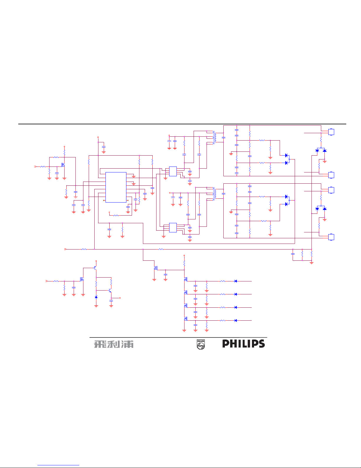
6.2 Power Board
715G1813-1
N
L903
C8B-R6H
1 2
R955
22K _NC
L
R953
1K 1/4W_NC
1 2
C915
0.012uF/25V
R917 33K
C913
0.1uF
12
R915 10
R927
4.7K_1206
12
-
+
BD901
U4KB80R
2
1
3
4
5VA
+
C927
68u/25V
R946
110K_1%
1 2
+12VCC
FB905
BEAD
C920
0.001uF/1KV
12
R910
1.5M/R1206
C903
0.001uF/250V
1 2
D918
1N4148
R944
9.1K/0805_1%
1 2
Lie down
C942
4.7nF/25V_NC
D931
MBRF10H100CT-45
NR901
SCK084
D926
RGP10D
12
TEA1532
IC901
TEA1532
4
128
5
36
7
FB901
BEAD
C914
1uF
12
D901
BYT42J
R932
2R2_1206
1 2
+
C933
1000uF/25V
+
C952
220u/25V
C901
0.001uF/250V
12
O
T901
POWER X'FMR
4
6
2
1
5
9
7
8
11
12
10
J912
12
R912
1M
1 2
R951
3.3K _NC
1 2
FB902
BEAD
C935
3.3nF/500V_NC
12
R920
0.2R/1W
R902
680K
1 2
C917
0.33uF/25V
+12VCC
VAR901
varistor_NC
R935
2R2_1206_NC
1 2
C900
0.001uF/250V
12
CN951
HARNESS 12P-12P 120mm
1
2
3
4
5
6
7
8
9
10
11
12
R904
1.5M/R1206
+
C907
100uF/450V
R926 0R
R942
27K _NC
12
R901
680K
1 2
+
C956
220u/16V
IC902
TCET1103
12
43
IC941
KIA431A
L951
0.8uH
1 2
C912
0.0022uF/400V
12
+12V
CN901
AC SOCKET
1 2
3
C955
0.1uF/25V
L955
0.8uH
1 2
S901
spotgap_NC
R945
9.1K_1%
1 2
R907
15K/R1206
R936
2R2_1206_NC
1 2
R905
100K/1W
L901
7mH
14
23
+5V
R941
220
BRIGHTNESS
+
C936
2200uF/16V
C951
0.1uF/25V
R914
1K24_1%
R900
680K
1 2
C941
0.0056uF
5VA
R952
10
1 2
ZD949
RLZ12B_NC
1 2
R916 1.5K
12
BL_CTL
D905
P4KE_NC
D919
RGP10D
12
+
C932
1000uF/25V
R937
1.8K_1/8W
1 2
F902
FUSE_5A/250V_NC
R949
100 1/10W_NC
1 2
C908
0.47uF/275V
12
PANEL_ID
L902
C8B-R6H
1 2
R918 150R
12
R931
2R2_1206
1 2
FB903
BEAD
S902
spotgap_NC
ZD975
RLZ5.1B
1 2
ZD951
P6KE8.2A
C931
3.3nF/500V
12
Q901
STP7NK80ZFP
1
23
F901
FUSE 3.15A 250V
1 21 2
D935
STPS10L45CFP
R954
10 1/10W
R943
5.1K 1/10W
1 2
R923 8K66_1%
12
Page 28
19” LCD Color Monitor 190P7
28
R887
100K 1/10W
12
C831
0.33uF
12
R812
620K 1/10W
12
Q841
AM9945N
1
2
3
4 5
6
7
8
S1
G1
S2
G2 D2
D2
D1
D1
D885
IN4148
C825
5PF/NC
1 2
Q871
2N7002
1
32
C812
0.1uF
12
Q886
2N7002
1
32
OP2
C823
0.001uF
1 2
C807
5pF/3KV
12
R843
10R
12
R872
10K/NC
1 2
D831
BAV99
3
1
2
R822
10R
12
D853
BAV70/SOT23B
3
1
2
R815
30K
R859
6.2M 1/2W
12
Q885
2N7002
1
32
Isen
C826
0.01uF/NC
R823
10R
12
R884
1K 1/10W
12
R871
10K 1/2W
12
OP3
Q880
2N7002
1
32
R839
6.2M 1/2W
12
R873
2K 1/10W
C887
0.01uF
Q873
PDTA144EU
3 1
2
R824
7.5K_1%_NC
1 2
VDD
OP2
C819
0.01uF/25V
12
R830
10K_1%_NC
12
D881
IN4148
OP4
C846
1uF
12
C844
5PF/NC
1 2
CN853
CONN
1
2
C805
5pF/3KV_NC
12
C842
0.001uF
1 2
VDD
R857
7.5K_NC
C858
390pF
C813
560pF
C832
0.1uF
12
C810
5pF/3KV_NC
12
C821
1uF
12
Q801
2N7002
1
32
Q874
2N3904
32
1
R804
10K 1/10W
12
D851
BAV99
3
1
2
PANEL_ID
OP1
C809
5pF/3KV_NC
12
C845
5PF/NC
1 2
D883
IN4148
C808
5pF/3KV
12
R855
10K_1%
ZD874
RLZ5.6B
1 2
OP4
Isen
C883
0.01uF
R861
100K_1%
12
C841
1uF
12
R866
100K/NC
12
+12V
R886
1K 1/10W
12
CN831
CONN
1
2
R883
100K 1/10W
12
C865
33nF
12
R835
10K_1%
1 2
C806
10pF/6KV
12
R819
1M
CN833
CONN
1
2
C860
220pF
12
CN851
CONN
1
2
C811
1uF
12
PT802
24:24:2400
7
1
3
85
6
2
4
R807
10K 1/10W
12
C840
470uF/25V
VDD
C820
470uF/25V
C822
0.001uF
1 2
PT801
24:24:2400
7
1
3
85
6
2
4
OP1
R833
1.2K
R801
10K
12
R854
6.2M_NC
12
+12V
R856
10K_1%
12
R880
10K 1/10W
12
R831
1K
R851
1K
R825
7.5K_1%
1 2
R806
100K/NC
1 2
C871
0.1uF_NC
C824
5PF/NC
1 2
C830
1000pF/NC
R834
6.2M 1/2W_NC
12
BL_CTL
OP3
R836
10K_1%
12
R874
330 1/10W
1 2
R803
10K/NC
12
C843
0.001uF
1 2
+12V
PANEL_ID
R802
10K/NC
1 2
C885
0.01uF
R850
10K_1%_NC
12
R882
1K 1/10W
12
R888
1K 1/10W
12
R853
1.2K
R885
100K 1/10W
12
Q821
AM9945N
1
2
3
4 5
6
7
8
S1
G1
S2
G2 D2
D2
D1
D1
R829
0 1/10W
C803
5pF/3KV
12
VDD
R865
232
C838
1000pF
Q883
2N7002
1
32
C801
10pF/6KV
12
R837
7.5K_1%
12
C847
0.022uF/25V
D887
IN4148
C802
5pF/3KV
12
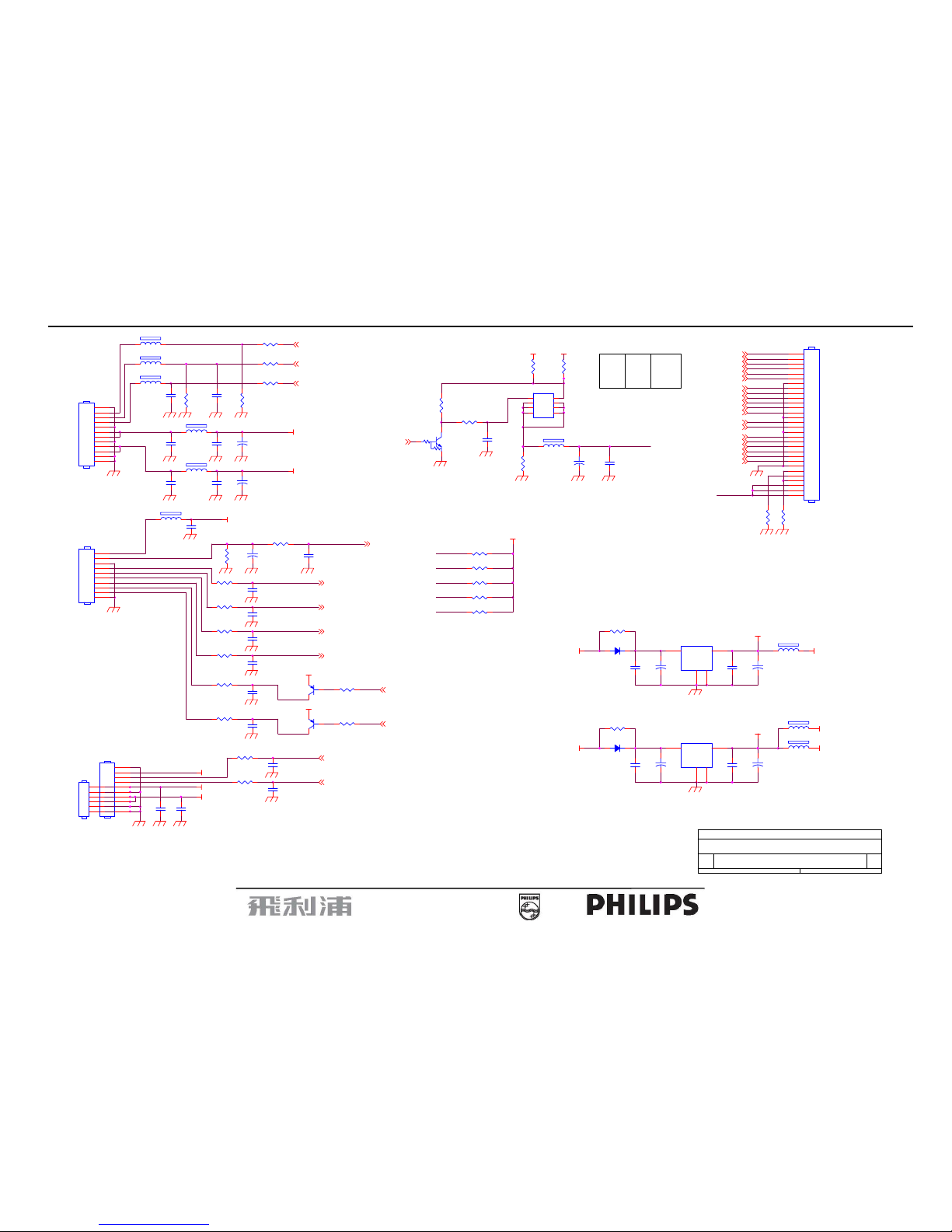
U811
OZ9938GN
1
2
3
4
5
6
7
8 9
10
11
12
13
14
15
16
DRV1
VDDA
TIMER
DIM
ISEN
VSEN
OVPT
NC1 NC2
ENA
LCT
SSTCMP
CT
GNDA
DRV2
PGND
C874
1uF
12
BRIGHTNESS
D833
BAV70/SOT23B
3
1
2
R849
0 1/10W
1 2
C880
0.1uF/25V
C861
1000pF
12
VDD
R881
100K 1/10W
12
R842
10R
12
R816
20K
C804
5pF/3KV_NC
12
R863
33K 1/4W
12
R813
33K_1%
R811
3M3
12
C881
0.01uF
Q881
2N7002
1
32
Page 29
19” LCD Color Monitor 190P7
29
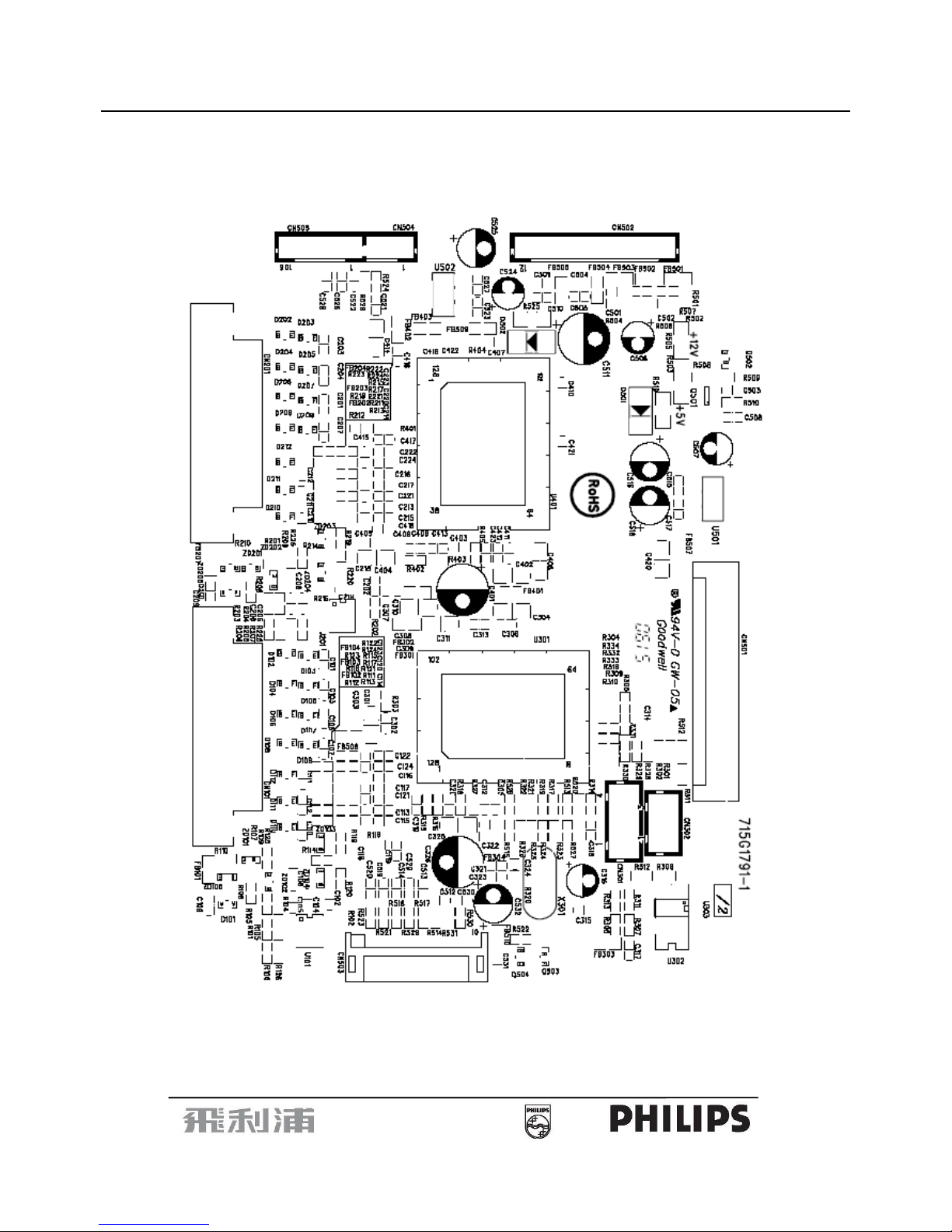
7. PCB Layout
7.1 Main Board
715G1791-1
Page 30

19” LCD Color Monitor 190P7
30
Page 31

19” LCD Color Monitor 190P7
31
Page 32

19” LCD Color Monitor 190P7
32
7.2 Power Board
715G1813-1
Page 33

19” LCD Color Monitor 190P7
33
Page 34

19” LCD Color Monitor 190P7
34
Page 35

19” LCD Color Monitor 190P7
35
7.3 Key Board
715G1805-1
7.4 USB Board
715G1794-1
Page 36

19” LCD Color Monitor 190P7
36
8. Wiring Diagram
Power Board
Panel
Main Board
Key Board
DVI
D
VI
A
C
-IN
CN851
CN853
CN831
CN833
CN951
CN901
CN001
CN201
CN101
CN502
CN505
USB Board
1601
1654
1651
CN503
1652
CN501
Page 37

19” LCD Color Monitor 190P7
37
9. Mechanical Instructions
Steps of dismantling base stand from base column
Step 1: Place the monitor face down on a smooth surface as Fig 1. Be careful to avoid scratch and injury during the
uninstallation. Meanwhile, it is need to avoid pressing the control key.
Fig1
Step 2: Unfasten one screw on the base stand as Fig 2.
Fig2
Page 38

19” LCD Color Monitor 190P7
38
Step 3: Firmly insert the base removal tool into four-pronged clicks as Fig 3.
Fig3
Step 4: Pull out the foot from base as Fig 4
.
Page 39

19” LCD Color Monitor 190P7
39
Page 40

19” LCD Color Monitor 190P7
40
Steps of assembling and disassembling side cover
1. Press down the rim of side cover and hold as Fig 1. (Press direction is toward panel surface side.)
Fig1
2. Pull out the side cover horizontally as Fig 2.
Fig2
Page 41

19” LCD Color Monitor 190P7
41
3. Tongues and grooves position on side cover and back cover as Fig 3.
Assembling the side cover:
1. Have 6 tongues on side cover aligned with back cover’s 6 grooves then push side cover horizontally into back cover.
Page 42

19” LCD Color Monitor 190P7
42
1. Back View as Fig.1
Fig.1
2. Remove base stand as Fig.2.
Remove the four screws to remove the base stand as Fig.2
Fig.2
Page 43

19” LCD Color Monitor 190P7
43
3. Disassembling the side covers as Fig.3.
Fig.3
Page 44

19” LCD Color Monitor 190P7
44
4. Remove rear cover as Fig.4.
Remove the four screws to remove the rear cover as Fig.4
Fig.4
5. Remove the shield as Fig.5
Remove the nine screws as Fig.5 to remove the shield.
Fig.5
Page 45
19” LCD Color Monitor 190P7
45
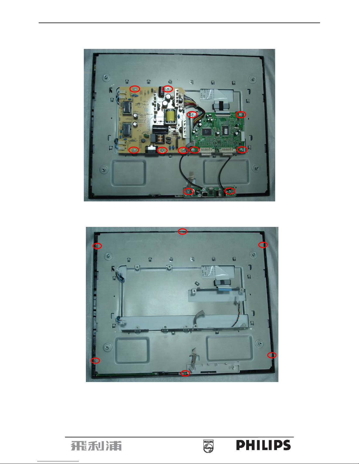
6. Remove the main board, the power board and the USB board as Fig.6
Remove the eleven screws as Fig.6 to remove the main board, the power board and the USB board.
Fig.6
7. Remove the front panel as Fig.7.
Remove the six screws as Fig.7 to remove the front panel.
Fig.7
Page 46

19” LCD Color Monitor 190P7
46
8. Remove the main frame as Fig.8
Remove the four screws as Fig.8 to remove the main frame.
Fig.8
Page 47

19” LCD Color Monitor 190P7
47
Page 48

19” LCD Color Monitor 190P7
48
10. Trouble Shooting
This page deals with problems that can be corrected by a user. If the problem still persists after you have tried
these solutions, contact Philips customer service representative.
Page 49

19” LCD Color Monitor 190P7
49
Page 50

19” LCD Color Monitor 190P7
50
11. Repair Flow Chart
(1). No Power
No power
Press power key and look if the
picture is normal
Please reinsert and make sure the
AC of 100-240 is normal
Reinsert or check the
p
ower section
X301 oscillate waveforms are
normal
Measure U502 Pin2=3.3V,
U501 Pin2=1.8V?
OK
OK
NG
NG
NG
Replace U501, U502
Replace U301, U401
Replace X301
OK
NG
Page 51

19” LCD Color Monitor 190P7
51
(2). No Picture
No picture
OK
OK
NG
NG
Measure U502 PIN2=3.3V,
U501 PIN2=1.8V?
Replace U501, U502
X301 oscillate waveforms are
normal
Replace X301
Check if the sync signal from
computer is output and video cable
is connected normally
Input the sync signal of
computer, or change
the cable
Replace U401, U301
NG
OK
Page 52

19” LCD Color Monitor 190P7
52
(3). White screen
(4). Keypad Board
White screen
Measure Q502 base
is high level?
X301 oscillate
waveform is normal
Check Q502, Q501 is broken
or CN406 solder?
Check Correspondent
Replace Panel
Check Correspondent
com
p
onent.
Replace U301
OK
OK
Replace X301
OK
NG
NG
NG
NG
Check reset circuit of
U401 is normal
OK
Page 53

19” LCD Color Monitor 190P7
53
9.2.2 Power/Inverter Board
No power
Adapter Board
Check CN951 pin 6/7 = 12V?
Check AC line volt 100-240V
Check AC input
Check the voltage of C907 (+)
Check bridge rectified circuit and F901 circuit
Check start voltage for the pin 8 of IC901
Check R907 and IC901
NG
Check the auxiliary voltage is bigger than
10V and smaller than 20V
Check IC901, D926, T901
OK
Check D931, D935, IC902, IC941, ZD975
OK
NG
NG
OK
OK
NG
NG
Page 54

19” LCD Color Monitor 190P7
54
Inverter board
No power
Check C811 (+) =5V
NG
OK
Check adapter section
Check ON/OFF signal
Check Interface section or main board
NG
OK
Check U811 pin 2=5V?
NG
OK
Check Q801
Check U811 Pin1/pin15 have the output of sawtooth wave at short time
NG
OK
Check U811 pin 5/pin6
NG
OK
Replace U811
Check Q821/Q841 pin5/pin8 is 12V?
Check PT801/PT802 pin7/pin8= 650V?
Cut all the pin connector of Q821/Q841, check C811 (+)=5V?
O
K
NG
Unplug backlight connector wire, check
PT801/PT802 pin7/pin8 = 650V?
OK
NG
Replace backlight
Replace PT801/PT802
OK
NG
NG
Replace Q821/Q841
Check Q801
OK
Page 55

19” LCD Color Monitor 190P7
55
12. ISP Instruction
(1). Install the program software
a. First decompressing files , as follow:
Page 56

19” LCD Color Monitor 190P7
56
b. Double – click
, start to install as follows:
Page 57

19” LCD Color Monitor 190P7
57
c. There will be a shortcut key appears on the desktop.
Page 58

19” LCD Color Monitor 190P7
58
(2). Connect the ISP board as follow:
a. Double-click
,running the program as follows:
Connect to
the PC LPT
Connect to the
Philips 190P by
a VGA to DVI-A
commutator as
below fig
Page 59

19” LCD Color Monitor 190P7
59
b. Click
icon, search the program” PHILIPS_190P7_NT68663_128K_LG19_EU_V1.00.hex”, and click
open:
c. Click icon, the writer is in processing…
Page 60

19” LCD Color Monitor 190P7
60
d. Until appears the follow Fig, writer completed.
Page 61

19” LCD Color Monitor 190P7
61
13. DDC Instruction
General
DDC Data Re-programming
In case the main EEPROM with Software DDC which store all factory settings were replaced because a defect,
repaired monitor’ the serial numbers have to be re-programmed.
It is advised to re- soldered the main EEPROM with Software DDC from the old board onto the new board if
circuit board have been replaced, in this case the DDC data does not need to be re-programmed.
Additional information about DDC (Display Data Channel) may be obtained from Video Electronics Standards
Association (VESA). Extended Display Identification Data (EDID) information may be also obtained from VESA.
13.1 DDC for OSD SN
System and equipment requirements
1.
An i486 (or above) personal computer or compatible.
2. Microsoft operation system Windows 95/98/2000/XP.
3.
“ PORT95NT, SerialNumberGlobal.exe、sn.ini” program.
4.
Software OSD SN Alignment kits
The kit contents:
a. OSD SN BOARD x1
b. Printer cablex1
c. VGA cable x1
d. 12V DC power source
1. Install the “PORT95NT.EXE”, and restart the computer.
Page 62

19” LCD Color Monitor 190P7
62
2. Connect the board as below
3. Run the “SerialNumberGlobel.exe”
Page 63

19” LCD Color Monitor 190P7
63
4. It will display as below:
5. Setting as below:
Page 64

19” LCD Color Monitor 190P7
64
6. Key in the new SN. Then click the “Start” icon.
7. When change SN success, there would be display “PASS” as below.
Page 65

19” LCD Color Monitor 190P7
65
Page 66

19” LCD Color Monitor 190P7
66
13.2 DDC for Monitor SN
System and equipment requirements
1. An i486 (or above) personal computer or compatible.
2. Microsoft operation system Windows 95/98/2000/XP.
3. “WinDDC, PORT95NT, config, W, CHECK, Philips 170S EDID” program.
4. Software DDC Alignment kits
The kit contents:
a. DDC Board x1
b. Printer cablex1
c. D-Sub cable x1
d. 12V DC power source
(1). Install software
You must install the at the first. The processing as follows:
Page 67

19” LCD Color Monitor 190P7
67
Page 68

19” LCD Color Monitor 190P7
68
Click
to complete the installation.
Note:
After installation, you must restart the PC to take the setup to effect.
(2). Connect the DDC board as follow:
Note: Pin5 of the VGA cable should be cut off.
Note: The 2 DVI-I ports should be respectively program.
Connect to the PC LPT
12V Input
Connect to the
Philips 190P by
a VGA to DVI-A
commutator as
below fig
Page 69

19” LCD Color Monitor 190P7
69
A. Program digital and analog EDID data
a. Double-click ,appear as follow Fig:
b. Key in ”1” as follow Figs:
Page 70

19” LCD Color Monitor 190P7
70
c. Press Enter key, then appears the following Fig:
d. Key in the Serial Number printed on the barcode label, then click “OK”
14 codes,
for example.
Page 71

19” LCD Color Monitor 190P7
71
e. When digital EDID program completed, appears the following Fig:
f. When ANALOG EDID program completed, appears the following Fig:
Page 72

19” LCD Color Monitor 190P7
72
B. Read digital and analog EDID data.
a. Key in ”2” as follow Figs:
b. Press Enter key, then appears the following Fig:
Page 73

19” LCD Color Monitor 190P7
73
c. Press Enter key to read analog as follow:
Page 74

19” LCD Color Monitor 190P7
74
128 bytes EDID Data (Hex):
x0 x1 x2 x3 x4 x5 x6 x7 x8 x9 xA xB xC xD xE xF
0: 00 FF FF FF FF FF FF 00 41 0C 41 08 01 00 00 00
10: 3E 0F 01 03 0E 26 1E 78 2A EF C0 A4 57 4A 9A 24
20: 12 50 54 BF EF 80 71 4F 81 40 81 80 01 01 01 01
30: 01 01 01 01 01 01 30 2A 00 98 51 00 2A 40 30 70
40: 13 00 78 2D 11 00 00 1E 00 00 00 FF 00 20 41 55
50: 20 20 30 30 30 30 30 31 0A 20 00 00 00 FC 00 50
60: 68 69 6C 69 70 73 20 31 39 30 50 0A 00 00 00 FD
70: 00 38 4C 1E 53 0E 00 0A 20 20 20 20 20 20 00 E1
Decoded EDID data
<---Header--->
Header: 00 FF FF FF FF FF FF 00
<-x-Header-x->
<---Vendor/Product Identification--->
ID Manufacturer Name: PHL
ID Product Code: 2113
ID Serial Number: 00000001
Week of Manufacture: 62
Year of Manufacture: 2005
<-x-Vendor/Product Identification-x->
<---EDID Structure Version/Revision--->
EDID Version#: 01
EDID Revision#: 03
<-x-EDID Structure Version/Revision-x->
<---Basic Display Parameters/Features--->
Video i/p definition: Analog
Signal Level Standard: 0.700V/0.300V(1.000Vpp)
Setup: Blank-to-Black not expected
Separate Sync Support: Yes
Composite Sync Support: Yes
Sync. on green video supported: Yes
Serration of the Vsync.Pulse is not required.
Max. H. Image Size : 38cm.
Max. V. Image Size : 30cm.
Display Gamma: 2.2
DPMS Features, Stand-by: No.
DPMS Features, Suspend: No.
DPMS Features, Active off: Yes.
Display Type: R.G.B color display.
Standard Default Color Space: R.G.B color.
Preferred Timing Mode: In First Detailed Timing.
GTF supported: No.
<---Basic Display Parameters/Features--->
<---Color Characteristics--->
Red x: 0.6435546875
Red y: 0.3417968750
Green x: 0.2939453125
Green y: 0.6044921875
Blue x: 0.1435546875
Blue y: 0.0703125000
White x: 0.3125000000
Page 75

19” LCD Color Monitor 190P7
75
White y: 0.3281250000
<-x-Color Characteristics-x->
<---Established Timings--->
Established Timings 1: BF
-720x400 @70Hz VGA,IBM
-640x480 @60Hz VGA,IBM
-640x480 @67Hz Apple,Mac II
-640x480 @72Hz VESA
-640x480 @75Hz VESA
-800x600 @56Hz VESA
-800x600 @60Hz VESA
Established Timings 2: EF
-800x600 @72Hz VESA
-800x600 @75Hz VESA
-832x624 @75Hz Apple,Mac II
-1024x768 @60Hz VESA
-1024x768 @70Hz VESA
-1024x768 @75Hz VESA
-1280x1024 @75Hz VESA
Established Timings 3: 80
-1152x870 @75Hz Apple,Mac II
<-x-Established Timings-x->
<---Standard Timing Identification--->
-1152x864 @75
-1280x960 @60
-1280x1024 @60
<-x-Standard Timing Identification-x->
<---Detailed Timing Descriptions--->
Detailed Timing: 1280x1024 @ 60Hz.
<-x-Detailed Timing Descriptions-x->
<---Detailed Timing Descriptions--->
Detailed Timing: FF (Monitor SN) ' AU 000001'
Detailed Timing: FC (Monitor Name) 'Philips 190P'
Detailed Timing: FD (Monitor limits)
Min. V. rate: 56Hz
Max. V. rate: 76Hz
Min. H. rate: 30KHz
Max. H. rate: 83KHz
Max. Pixel Clock: 140MHz
<-x-Detailed Timing Descriptions-x->
Extension Flag: 00
Checksum: E1
Page 76

19” LCD Color Monitor 190P7
76
128 bytes EDID Data (Hex):
x0 x1 x2 x3 x4 x5 x6 x7 x8 x9 xA xB xC xD xE xF
0: 00 FF FF FF FF FF FF 00 41 0C 41 08 01 00 00 00
10: 3E 0F 01 03 80 26 1E 78 2A EF C0 A4 57 4A 9A 24
20: 12 50 54 BF EF 80 71 4F 81 40 81 80 01 01 01 01
30: 01 01 01 01 01 01 30 2A 00 98 51 00 2A 40 30 70
40: 13 00 78 2D 11 00 00 1E 00 00 00 FF 00 20 41 55
50: 20 20 30 30 30 30 30 31 0A 20 00 00 00 FC 00 50
60: 68 69 6C 69 70 73 20 31 39 30 50 0A 00 00 00 FD
70: 00 38 4C 1E 53 0E 00 0A 20 20 20 20 20 20 00 6F
Decoded EDID data
<---Header--->
Header: 00 FF FF FF FF FF FF 00
<-x-Header-x->
<---Vendor/Product Identification--->
ID Manufacturer Name: PHL
ID Product Code: 2113
ID Serial Number: 00000001
Week of Manufacture: 62
Year of Manufacture: 2005
<-x-Vendor/Product Identification-x->
<---EDID Structure Version/Revision--->
EDID Version#: 01
EDID Revision#: 03
<-x-EDID Structure Version/Revision-x->
<---Basic Display Parameters/Features--->
Video i/p definition: Digital
Max. H. Image Size : 38cm.
Max. V. Image Size : 30cm.
Display Gamma: 2.2
DPMS Features, Stand-by: No.
DPMS Features, Suspend: No.
DPMS Features, Active off: Yes.
Display Type: R.G.B color display.
Standard Default Color Space: R.G.B color.
Preferred Timing Mode: In First Detailed Timing.
GTF supported: No.
<---Basic Display Parameters/Features--->
<---Color Characteristics--->
Red x: 0.6435546875
Red y: 0.3417968750
Green x: 0.2939453125
Green y: 0.6044921875
Blue x: 0.1435546875
Blue y: 0.0703125000
White x: 0.3125000000
White y: 0.3281250000
<-x-Color Characteristics-x->
<---Established Timings--->
Established Timings 1: BF
-720x400 @70Hz VGA,IBM
Page 77

19” LCD Color Monitor 190P7
77
-640x480 @60Hz VGA,IBM
-640x480 @67Hz Apple,Mac II
-640x480 @72Hz VESA
-640x480 @75Hz VESA
-800x600 @56Hz VESA
-800x600 @60Hz VESA
Established Timings 2: EF
-800x600 @72Hz VESA
-800x600 @75Hz VESA
-832x624 @75Hz Apple,Mac II
-1024x768 @60Hz VESA
-1024x768 @70Hz VESA
-1024x768 @75Hz VESA
-1280x1024 @75Hz VESA
Established Timings 3: 80
-1152x870 @75Hz Apple,Mac II
<-x-Established Timings-x->
<---Standard Timing Identification--->
-1152x864 @75
-1280x960 @60
-1280x1024 @60
<-x-Standard Timing Identification-x->
<---Detailed Timing Descriptions--->
Detailed Timing: 1280x1024 @ 60Hz.
<-x-Detailed Timing Descriptions-x->
<---Detailed Timing Descriptions--->
Detailed Timing: FF (Monitor SN) ' AU 000001'
Detailed Timing: FC (Monitor Name) 'Philips 190P'
Detailed Timing: FD (Monitor limits)
Min. V. rate: 56Hz
Max. V. rate: 76Hz
Min. H. rate: 30KHz
Max. H. rate: 83KHz
Max. Pixel Clock: 140MHz
<-x-Detailed Timing Descriptions-x->
Extension Flag: 00
Checksum: 6F
Page 78

19” LCD Color Monitor 190P7
78
14. White Balance, Luminance Adjustment
Approximately 30 minutes should be allowed for warm up before proceeding White-Balance adjustment.
1. Required instruments: Chroma 7120、Chroma 2325(BGA265A)。
2. First connect the instruments together and turn on the LCD power.
3. Set Chroma 2325(BGA265A)to be T144(1280*1024/60HZ)and P105 of full white screen.
4. Enter into the factory mode:
Firstly, turn off the power, press the AUTO and OK at the same time, and then turn the power on (AUTO and OK
are still pressed, about 10s), release, press the menu again will activate the factory mode, the factory OSD will
be at the left top of the screen.
Move the cursor to select the Hyson 190P7***********, press OK button to enter into the sub-menu; Move the
cursor again to select ” Cool/warm “.
5. Set Chroma-7120 CH3 as 9300 color temperature by ID key, press SC and Next key set 9300K: x=283±20,
y=297±20,Y>200.
Set Chroma-7120 CH4 as 6500 color temperature by ID key, press SC and Next key set 6500K: x=313±20,
y=329±20,Y>230.
6. Adjust 9300K color temperature:
1). Switch the Chroma-7120 to RGB-Mode (with press “MODE” button)
2). Switch the MEM. Channel to Channel 3 (with up or down arrow on chroma 7120)
3). Adjust the R of Cool item on factory window until chroma 7120 indicator reached the value R=100±5
4). Adjust the G of Cool item on factory window until chroma 7120 indicator reached the value G=100±5
5). Adjust the B of Cool item on factory window until chroma 7120 indicator reached the value B=100±5
6). Switch the Chroma-7120 to x, y, Y Mode (with press “MODE” button), check whether the color-temperature
value is within Spec (the Spec is 9300: x=283±20, y=297±20,Y>200). If not in the SPEC, repeat step 3,4,5.
7. Adjust 6500K/SRGB color temperature:
1). Switch the Chroma-7120 to RGB-Mode (with press “MODE” button)
2). Switch the MEM. Channel to Channel 4 (with up or down arrow on chroma 7120)
3). Adjust the R of Warm item on factory window until chroma 7120 indicator reached the value R=100±5
4). Adjust the G of Warm item on factory window until chroma 7120 indicator reached the value G=100±5
5). Adjust the B of Warm item on factory window until chroma 7120 indicator reached the value B=100±5
6). Switch the Chroma-7120 to x, y, Y Mode, check whether the color-temperature value is within Spec.
the Spec is 6500: x=313±20, y=329±20,Y>230. If not in the SPEC, repeat step 3,4,5.
Turn the Power-button off to quit and save the factory mode.
Page 79

19” LCD Color Monitor 190P7
79
15. Recommended&Spare Parts List
Service Kit
Description Part No. Philips 12NC Remark
DDC Kit 715L2005C2 9965 000 43197 For all philips model
OSD SN Kit 715GT033 C 9965 000 43252 For all philips model
NOVATEK ISP Kit 715LT035A 9965 000 43198
For all philips hudson 7
For 190B8,170B8,170A8,190A8,170P8,
170S8,190S8,170V8,190V8,150S8
MSTAR ISP Kit
200CW8M,190P8
REALTEK ISP Kit
170CW8
Recommended Parts List
190P7ES/00
Location Part No for TPV Description Philips 12NC
750GLU90G0111M PANEL LCD 19" EG01 V0 PHILIPS AU 9965 000 37757
CBPC986KAMPHUP CONVERSION BOARD ASS'Y 9965 000 37767
KEPC986KHUP KEY BOARD ASS'Y 9965 000 37769
PWPC1942LGR2P POWER BOARD ASS'Y 9965 000 37768
USB986A1P USB BOARD ASS'Y 9965 000 37770
089G179E30C902 FFC CABLE P-TWO 9965 000 37756
089G175921 USB CABLE 9965 000 37753
P15G83322 MAINFRAME_LPL 9965 000 37758
P33G500811C BUTTON_POWER 9965 000 37759
P33G5009VP1L BUTTON_FUNC 9965 000 37760
P33G5010VB1T STAND_USB 9965 000 37761
P34G1868VOA1T BEZEL 9965 000 37762
P34G1869VB1T REAR_COVER 9965 000 37763
P34G1870VP1T COVER_SIDE 9965 000 37764
P37G5661VO BASE ASS'Y 9965 000 37765
Q15G00391 JIG 9965 000 37766
U301 056G562117 IC NT68663MEFG-128 QFP-128L NOVA 9965 000 37779
U401 056G562512 NT68563EFG 9965 000 37780
U502 056G563806 IC AIC1187-33PY SOT-223 AIC 9965 000 37781
U501 056G563807 IC AIC1187-18PY SOT-223 AIC 9965 000 37782
U303 056G113356 M24C16-WMN6TP 9965 000 37783
U101 056G1133902 IC BU9882FV-W SSOP14 ROHM 9965 000 37784
U201 056G1133902 IC BU9882FV-W SSOP14 ROHM 9965 000 37784
U811 056G60810 0Z9938 9965 000 36059
IC902 056G1393A PC123Y22FZOF 9965 000 36055
IC901 056G564911 IC TEA1532AT S08 9965 000 36960
IC941 056G15810T AZ431AZ-AE1 9965 000 36101
Page 80

19” LCD Color Monitor 190P7
80
Spare Parts List
190P7ES/00
Panel
Part No for TPV Description Philips 12NC
750GLU90G0111M PANEL LCD 19" EG01 V0 PHILIPS AU 9965 000 37757
Board Ass’y
Part No for TPV Description Philips 12NC
CBPC986KAMPHUP CONVERSION BOARD ASS'Y 9965 000 37767
KEPC986KHUP KEY BOARD ASS'Y 9965 000 37769
PWPC1942LGR2P POWER BOARD ASS'Y 9965 000 37768
USB986A1P USB BOARD ASS'Y 9965 000 37770
Accessory and Mechanical
Part No for TPV
Description
Philips 12NC
089G179E30C902 FFC CABLE P-TWO 9965 000 37756
089G175921 USB CABLE 9965 000 37753
P15G83322 MAINFRAME_LPL 9965 000 37758
P33G500811C BUTTON_POWER 9965 000 37759
P33G5009VP1L BUTTON_FUNC 9965 000 37760
P33G5010VB1T STAND_USB 9965 000 37761
P34G1868VOA1T BEZEL 9965 000 37762
P34G1869VB1T REAR_COVER 9965 000 37763
P34G1870VP1T COVER_SIDE 9965 000 37764
P37G5661VO BASE ASS'Y 9965 000 37765
Q15G00391 JIG 9965 000 37766
Page 81

19” LCD Color Monitor 190P7
81
Main Board
Location Part No. for TPV Description Philips 12NC
C316 067G3051007C
105 10UF M 50V
9965 000 37771
C507 067G3051007C
105 10UF M 50V
9965 000 37771
C511 067G3052214C
105 220UF M 25V
9965 000 37772
C506 067G3054707C
105 47UF M 50V
9965 000 37773
C401 067G3054713C
105 470UF M 16V
9965 000 37774
C326 067G3054713C
105 470UF M 16V
9965 000 37774
C516 067G215P1007C
105 10UF M 50V
9965 000 37775
C524 067G215P1007C
105 10UF M 50V
9965 000 37775
C518 067G215P1014C
105 100UF M 25V
9965 000 37776
C525 067G215P1014C
105 100UF M 25V
9965 000 37776
C532 067G305V2203
105 22UF -20% 16V
9965 000 37777
CN101 088G35428FH DVI CONN R/A 28P 9965 000 37778
CN201 088G35428FH DVI CONN R/A 28P 9965 000 37778
X301 093G2251 CRYSTAL 12MHZ HC-49US ARG6-120 9965 000 35961
U301 056G562117 IC NT68663MEFG-128 QFP-128L NOVA 9965 000 37779
705G 56G PH304 CPU ASS'Y (CBPC986KAMPHUP) 996500041841
U502 056G563806 IC AIC1187-33PY SOT-223 AIC 9965 000 37781
U501 056G563807 IC AIC1187-18PY SOT-223 AIC 9965 000 37782
U303 056G113356 M24C16-WMN6TP 9965 000 37783
U101 056G1133902 IC BU9882FV-W SSOP14 ROHM 9965 000 37784
U201 056G1133902 IC BU9882FV-W SSOP14 ROHM 9965 000 37784
Q504 057G420519T TRA SIG SM BC857CG (ONSE) R 9965 000 37785
Q503 057G420519T TRA SIG SM BC857CG (ONSE) R 9965 000 37785
Q502 057G7601PH TRA SIG SM MUN2211J(ONSE)R 9965 000 37397
Q501 057G7631PH FET POW SM SI5441DC(VISH)R 9965 000 37398
R517 061L0603101 CHIPR 100 OHM -5% 1/16W 9965 000 35969
R405 061L0603101 CHIPR 100 OHM -5% 1/16W 9965 000 35969
R403 061L0603101 CHIPR 100 OHM -5% 1/16W 9965 000 35969
R402 061L0603101 CHIPR 100 OHM -5% 1/16W 9965 000 35969
R316 061L0603101 CHIPR 100 OHM -5% 1/16W 9965 000 35969
R315 061L0603101 CHIPR 100 OHM -5% 1/16W 9965 000 35969
R312 061L0603101 CHIPR 100 OHM -5% 1/16W 9965 000 35969
R311 061L0603101 CHIPR 100 OHM -5% 1/16W 9965 000 35969
R304 061L0603101 CHIPR 100 OHM -5% 1/16W 9965 000 35969
R302 061L0603101 CHIPR 100 OHM -5% 1/16W 9965 000 35969
R301 061L0603101 CHIPR 100 OHM -5% 1/16W 9965 000 35969
R216 061L0603101 CHIPR 100 OHM -5% 1/16W 9965 000 35969
R214 061L0603101 CHIPR 100 OHM -5% 1/16W 9965 000 35969
R116 061L0603101 CHIPR 100 OHM -5% 1/16W 9965 000 35969
R114 061L0603101 CHIPR 100 OHM -5% 1/16W 9965 000 35969
R529 061L0603102 CHIPR 1K OHM -5% 1/16W 9965 000 35970
Page 82

19” LCD Color Monitor 190P7
82
R514 061L0603102 CHIPR 1K OHM -5% 1/16W 9965 000 35970
R518 061L0603102 CHIPR 1K OHM -5% 1/16W 9965 000 35970
R210 061L0603102 CHIPR 1K OHM -5% 1/16W 9965 000 35970
R209 061L0603102 CHIPR 1K OHM -5% 1/16W 9965 000 35970
R110 061L0603102 CHIPR 1K OHM -5% 1/16W 9965 000 35970
R109 061L0603102 CHIPR 1K OHM -5% 1/16W 9965 000 35970
R225 061L0603103 CHIPR 10K OHM -5% 1/16W 9965 000 35971
R306 061L0603103 CHIPR 10K OHM -5% 1/16W 9965 000 35971
R314 061L0603103 CHIPR 10K OHM -5% 1/16W 9965 000 35971
R404 061L0603103 CHIPR 10K OHM -5% 1/16W 9965 000 35971
R510 061L0603103 CHIPR 10K OHM -5% 1/16W 9965 000 35971
R513 061L0603103 CHIPR 10K OHM -5% 1/16W 9965 000 35971
R515 061L0603103 CHIPR 10K OHM -5% 1/16W 9965 000 35971
R516 061L0603103 CHIPR 10K OHM -5% 1/16W 9965 000 35971
R520 061L0603103 CHIPR 10K OHM -5% 1/16W 9965 000 35971
R522 061L0603103 CHIPR 10K OHM -5% 1/16W 9965 000 35971
R527 061L0603103 CHIPR 10K OHM -5% 1/16W 9965 000 35971
R528 061L0603103 CHIPR 10K OHM -5% 1/16W 9965 000 35971
R207 061L0603103 CHIPR 10K OHM -5% 1/16W 9965 000 35971
R101 061L0603103 CHIPR 10K OHM -5% 1/16W 9965 000 35971
R102 061L0603103 CHIPR 10K OHM -5% 1/16W 9965 000 35971
R103 061L0603103 CHIPR 10K OHM -5% 1/16W 9965 000 35971
R104 061L0603103 CHIPR 10K OHM -5% 1/16W 9965 000 35971
R105 061L0603103 CHIPR 10K OHM -5% 1/16W 9965 000 35971
R106 061L0603103 CHIPR 10K OHM -5% 1/16W 9965 000 35971
R125 061L0603103 CHIPR 10K OHM -5% 1/16W 9965 000 35971
R202 061L0603103 CHIPR 10K OHM -5% 1/16W 9965 000 35971
R203 061L0603103 CHIPR 10K OHM -5% 1/16W 9965 000 35971
R204 061L0603103 CHIPR 10K OHM -5% 1/16W 9965 000 35971
R205 061L0603103 CHIPR 10K OHM -5% 1/16W 9965 000 35971
R206 061L0603103 CHIPR 10K OHM -5% 1/16W 9965 000 35971
R509 061L0603104 RST SM 0603 RC0603 100K PM5 R 9965 000 35972
R320 061L0603105 RST SM 0603 RC0603 1M PM5 R 9965 000 35973
R224 061L0603151 CHIPR 150 OHM -5% 1/16W 9965 000 35974
R221 061L0603151 CHIPR 150 OHM -5% 1/16W 9965 000 35974
R213 061L0603151 CHIPR 150 OHM -5% 1/16W 9965 000 35974
R124 061L0603151 CHIPR 150 OHM -5% 1/16W 9965 000 35974
R121 061L0603151 CHIPR 150 OHM -5% 1/16W 9965 000 35974
R113 061L0603151 CHIPR 150 OHM -5% 1/16W 9965 000 35974
R318 061L0603220 CHIPR 22 OHM -5% 1/16W 9965 000 37786
R531 061L06032201F 2.2K OHM 1% 1/10W 9965 000 37787
R523 061L0603221 CHIPR 220 OHM -5% 1/16W 9965 000 35976
R521 061L0603221 CHIPR 220 OHM -5% 1/16W 9965 000 35976
Page 83

19” LCD Color Monitor 190P7
83
R119 061L0603222 CHIPR 2.2K OHM -5% 1/16W 9965 000 35977
R120 061L0603222 CHIPR 2.2K OHM -5% 1/16W 9965 000 35977
R219 061L0603222 CHIPR 2.2K OHM -5% 1/16W 9965 000 35977
R220 061L0603222 CHIPR 2.2K OHM -5% 1/16W 9965 000 35977
R401 061L0603391 CHIP 390 OHM 1/10W 9965 000 37788
R303 061L0603391 CHIP 390 OHM 1/10W 9965 000 37788
R215 061L0603391 CHIP 390 OHM 1/10W 9965 000 37788
R115 061L0603391 CHIP 390 OHM 1/10W 9965 000 37788
R322 061L0603470 CHIPR 47 OHM -5% 1/16W 9965 000 35980
R321 061L0603470 CHIPR 47 OHM -5% 1/16W 9965 000 35980
R319 061L0603470 CHIPR 47 OHM -5% 1/16W 9965 000 35980
R317 061L0603470 CHIPR 47 OHM -5% 1/16W 9965 000 35980
R208 061L0603470 CHIPR 47 OHM -5% 1/16W 9965 000 35980
R201 061L0603470 CHIPR 47 OHM -5% 1/16W 9965 000 35980
R108 061L0603470 CHIPR 47 OHM -5% 1/16W 9965 000 35980
R107 061L0603470 CHIPR 47 OHM -5% 1/16W 9965 000 35980
R530 061L0603470 CHIPR 47 OHM -5% 1/16W 9965 000 35980
R504 061L0603470 CHIPR 47 OHM -5% 1/16W 9965 000 35980
R502 061L0603470 CHIPR 47 OHM -5% 1/16W 9965 000 35980
R501 061L0603470 CHIPR 47 OHM -5% 1/16W 9965 000 35980
R334 061L0603472 CHIPR 4.7K OHM -5% 1/16W 9965 000 35981
R333 061L0603472 CHIPR 4.7K OHM -5% 1/16W 9965 000 35981
R332 061L0603472 CHIPR 4.7K OHM -5% 1/16W 9965 000 35981
R331 061L0603472 CHIPR 4.7K OHM -5% 1/16W 9965 000 35981
R327 061L0603472 CHIPR 4.7K OHM -5% 1/16W 9965 000 35981
R310 061L0603472 CHIPR 4.7K OHM -5% 1/16W 9965 000 35981
R309 061L0603472 CHIPR 4.7K OHM -5% 1/16W 9965 000 35981
R308 061L0603472 CHIPR 4.7K OHM -5% 1/16W 9965 000 35981
R307 061L0603472 CHIPR 4.7K OHM -5% 1/16W 9965 000 35981
R508 061L0603473 RST SM 0603 RC0603 47K PM5 R 9965 000 36003
R222 061L0603750 CHIPR 75 OHM -5% 1/16W 9965 000 35982
R217 061L0603750 CHIPR 75 OHM -5% 1/16W 9965 000 35982
R211 061L0603750 CHIPR 75 OHM -5% 1/16W 9965 000 35982
R122 061L0603750 CHIPR 75 OHM -5% 1/16W 9965 000 35982
R117 061L0603750 CHIPR 75 OHM -5% 1/16W 9965 000 35982
R111 061L0603750 CHIPR 75 OHM -5% 1/16W 9965 000 35982
R112 061L06037509F 75OHM 1% 1/10W 9965 000 35983
R118 061L06037509F 75OHM 1% 1/10W 9965 000 35983
R123 061L06037509F 75OHM 1% 1/10W 9965 000 35983
R212 061L06037509F 75OHM 1% 1/10W 9965 000 35983
R218 061L06037509F 75OHM 1% 1/10W 9965 000 35983
R223 061L06037509F 75OHM 1% 1/10W 9965 000 35983
R503 061L1206000 CHIPR 0 OHM -5% 1/8W 9965 000 36067
Page 84

19” LCD Color Monitor 190P7
84
C530 065G060310231 CHIP 1000PF 50V NPO 9965 000 36917
C520 065G060310231 CHIP 1000PF 50V NPO 9965 000 36917
C519 065G060310231 CHIP 1000PF 50V NPO 9965 000 36917
C502 065G060310412 CER2 0603 X7R 16V 100N PM10 R 9965 000 36918
C501 065G060310412 CER2 0603 X7R 16V 100N PM10 R 9965 000 36918
C423 065G060310412 CER2 0603 X7R 16V 100N PM10 R 9965 000 36918
C422 065G060310412 CER2 0603 X7R 16V 100N PM10 R 9965 000 36918
C421 065G060310412 CER2 0603 X7R 16V 100N PM10 R 9965 000 36918
C419 065G060310412 CER2 0603 X7R 16V 100N PM10 R 9965 000 36918
C418 065G060310412 CER2 0603 X7R 16V 100N PM10 R 9965 000 36918
C417 065G060310412 CER2 0603 X7R 16V 100N PM10 R 9965 000 36918
C416 065G060310412 CER2 0603 X7R 16V 100N PM10 R 9965 000 36918
C415 065G060310412 CER2 0603 X7R 16V 100N PM10 R 9965 000 36918
C412 065G060310412 CER2 0603 X7R 16V 100N PM10 R 9965 000 36918
C411 065G060310412 CER2 0603 X7R 16V 100N PM10 R 9965 000 36918
C531 065G060310412 CER2 0603 X7R 16V 100N PM10 R 9965 000 36918
C528 065G060310412 CER2 0603 X7R 16V 100N PM10 R 9965 000 36918
C527 065G060310412 CER2 0603 X7R 16V 100N PM10 R 9965 000 36918
C526 065G060310412 CER2 0603 X7R 16V 100N PM10 R 9965 000 36918
C523 065G060310412 CER2 0603 X7R 16V 100N PM10 R 9965 000 36918
C517 065G060310412 CER2 0603 X7R 16V 100N PM10 R 9965 000 36918
C515 065G060310412 CER2 0603 X7R 16V 100N PM10 R 9965 000 36918
C510 065G060310412 CER2 0603 X7R 16V 100N PM10 R 9965 000 36918
C509 065G060310412 CER2 0603 X7R 16V 100N PM10 R 9965 000 36918
C508 065G060310412 CER2 0603 X7R 16V 100N PM10 R 9965 000 36918
C505 065G060310412 CER2 0603 X7R 16V 100N PM10 R 9965 000 36918
C504 065G060310412 CER2 0603 X7R 16V 100N PM10 R 9965 000 36918
C307 065G060310412 CER2 0603 X7R 16V 100N PM10 R 9965 000 36918
C306 065G060310412 CER2 0603 X7R 16V 100N PM10 R 9965 000 36918
C305 065G060310412 CER2 0603 X7R 16V 100N PM10 R 9965 000 36918
C303 065G060310412 CER2 0603 X7R 16V 100N PM10 R 9965 000 36918
C302 065G060310412 CER2 0603 X7R 16V 100N PM10 R 9965 000 36918
C209 065G060310412 CER2 0603 X7R 16V 100N PM10 R 9965 000 36918
C208 065G060310412 CER2 0603 X7R 16V 100N PM10 R 9965 000 36918
C202 065G060310412 CER2 0603 X7R 16V 100N PM10 R 9965 000 36918
C109 065G060310412 CER2 0603 X7R 16V 100N PM10 R 9965 000 36918
C108 065G060310412 CER2 0603 X7R 16V 100N PM10 R 9965 000 36918
C102 065G060310412 CER2 0603 X7R 16V 100N PM10 R 9965 000 36918
C317 065G060310412 CER2 0603 X7R 16V 100N PM10 R 9965 000 36918
C410 065G060310412 CER2 0603 X7R 16V 100N PM10 R 9965 000 36918
C409 065G060310412 CER2 0603 X7R 16V 100N PM10 R 9965 000 36918
C407 065G060310412 CER2 0603 X7R 16V 100N PM10 R 9965 000 36918
C405 065G060310412 CER2 0603 X7R 16V 100N PM10 R 9965 000 36918
Page 85

19” LCD Color Monitor 190P7
85
C403 065G060310412 CER2 0603 X7R 16V 100N PM10 R 9965 000 36918
C322 065G060310412 CER2 0603 X7R 16V 100N PM10 R 9965 000 36918
C318 065G060310412 CER2 0603 X7R 16V 100N PM10 R 9965 000 36918
C315 065G060310412 CER2 0603 X7R 16V 100N PM10 R 9965 000 36918
C313 065G060310412 CER2 0603 X7R 16V 100N PM10 R 9965 000 36918
C312 065G060310412 CER2 0603 X7R 16V 100N PM10 R 9965 000 36918
C310 065G060310412 CER2 0603 X7R 16V 100N PM10 R 9965 000 36918
C308 065G060310412 CER2 0603 X7R 16V 100N PM10 R 9965 000 36918
C324 065G060322031 CER1 0603 NP0 50V 22P PM5 R 9965 000 36919
C323 065G060322031 CER1 0603 NP0 50V 22P PM5 R 9965 000 36919
C321 065G060322031 CER1 0603 NP0 50V 22P PM5 R 9965 000 36919
C119 065G060322131 CER1 0603 NP0 50V 220P PM5 R 9965 000 37789
C219 065G060322131 CER1 0603 NP0 50V 220P PM5 R 9965 000 37789
C118 065G060333031 CER1 0603 NP0 50V 33P PM5 R 9965 000 37790
C218 065G060333031 CER1 0603 NP0 50V 33P PM5 R 9965 000 37790
C206 065G060333131 330PF -5% 50V NPO 9965 000 37791
C205 065G060333131 330PF -5% 50V NPO 9965 000 37791
C105 065G060333131 330PF -5% 50V NPO 9965 000 37791
C104 065G060333131 330PF -5% 50V NPO 9965 000 37791
C224 065G060347332 CHIP 0.047UF 50V X7R 9965 000 36921
C222 065G060347332 CHIP 0.047UF 50V X7R 9965 000 36921
C221 065G060347332 CHIP 0.047UF 50V X7R 9965 000 36921
C217 065G060347332 CHIP 0.047UF 50V X7R 9965 000 36921
C216 065G060347332 CHIP 0.047UF 50V X7R 9965 000 36921
C215 065G060347332 CHIP 0.047UF 50V X7R 9965 000 36921
C213 065G060347332 CHIP 0.047UF 50V X7R 9965 000 36921
C113 065G060347332 CHIP 0.047UF 50V X7R 9965 000 36921
C115 065G060347332 CHIP 0.047UF 50V X7R 9965 000 36921
C116 065G060347332 CHIP 0.047UF 50V X7R 9965 000 36921
C117 065G060347332 CHIP 0.047UF 50V X7R 9965 000 36921
C121 065G060347332 CHIP 0.047UF 50V X7R 9965 000 36921
C122 065G060347332 CHIP 0.047UF 50V X7R 9965 000 36921
C124 065G060347332 CHIP 0.047UF 50V X7R 9965 000 36921
C420 065G120610617 CHIP 10UF 16V Y5V 9965 000 37402
C414 065G120610617 CHIP 10UF 16V Y5V 9965 000 37402
C406 065G120610617 CHIP 10UF 16V Y5V 9965 000 37402
C404 065G120610617 CHIP 10UF 16V Y5V 9965 000 37402
C402 065G120610617 CHIP 10UF 16V Y5V 9965 000 37402
C325 065G120610617 CHIP 10UF 16V Y5V 9965 000 37402
C311 065G120610617 CHIP 10UF 16V Y5V 9965 000 37402
C309 065G120610617 CHIP 10UF 16V Y5V 9965 000 37402
C304 065G120610617 CHIP 10UF 16V Y5V 9965 000 37402
C301 065G120610617 CHIP 10UF 16V Y5V 9965 000 37402
Page 86

19” LCD Color Monitor 190P7
86
D101 093G6442P DIO SW BAV70 SOT23 9965 000 13591
D201 093G6442P DIO SW BAV70 SOT23 9965 000 13591
ZD205 093G39S66 DIO REG SM BZX84-C5V1 (PHSE)R 9965 000 37792
ZD204 093G39S66 DIO REG SM BZX84-C5V1 (PHSE)R 9965 000 37792
ZD203 093G39S66 DIO REG SM BZX84-C5V1 (PHSE)R 9965 000 37792
ZD105 093G39S66 DIO REG SM BZX84-C5V1 (PHSE)R 9965 000 37792
ZD104 093G39S66 DIO REG SM BZX84-C5V1 (PHSE)R 9965 000 37792
ZD103 093G39S66 DIO REG SM BZX84-C5V1 (PHSE)R 9965 000 37792
D501 093G1020PH DIODE S1D-E3 VISHAY 9965 000 37793
D502 093G1020PH DIODE S1D-E3 VISHAY 9965 000 37793
Page 87

19” LCD Color Monitor 190P7
87
Power Board
Location Part No. for TPV Description Philips 12NC
IC902 056G1393A PC123Y22FZOF 9965 000 36055
NR901 061G5810T 8 OHM 4A NTCR BY THINKING 9965 000 36938
R905 061G152M10464 100KOHM 5% 2W 9965 000 36939
R920 061G152M20864 0.20 OHM 2W 9965 000 36940
C908 063G10747410S FILM CAPACITOR 9965 000 37794
C808 065G3J5096ET 5PF 5% SL 3KV 9965 000 36941
C807 065G3J5096ET 5PF 5% SL 3KV 9965 000 36941
C803 065G3J5096ET 5PF 5% SL 3KV 9965 000 36941
C802 065G3J5096ET 5PF 5% SL 3KV 9965 000 36941
C801 065G6J1006ET 10PF 5% SL 6KV 9965 000 36942
C806 065G6J1006ET 10PF 5% SL 6KV 9965 000 36942
C900 065G305M1022BP Y2 1000PF M 250VAC Y5P 9965 000 36943
C901 065G305M1022BP Y2 1000PF M 250VAC Y5P 9965 000 36943
C912 065G305M2222BP 2200PF -20% 9965 000 36944
C936 067G215D2222KV
105∑ 2200UF M 10V
9965 000 36945
C840 067G215D4714K ED 470UF 25V 9965 000 36007
C907 067G215S10115K 100UF 450V 9965 000 36086
C933 067G215S1024K ED1000UF 25V 9965 000 36946
C932 067G215S1024K ED1000UF 25V 9965 000 36946
L902 071G5524 FERRITE BEAD 9965 000 36947
L903 071G5524 FERRITE BEAD 9965 000 36947
L901 073G17465LS LINE FILTER BY LISHIN 9965 000 36025
L951 073G253902T CKOLE COIL 0.8UH 9965 000 36948
L955 073G253902T CKOLE COIL 0.8UH 9965 000 36948
T901 080GL17T900T X'FMR SRW28LEC-T93H016 9965 000 36950
PT801 080GL19T8DN1 X'FMR DARFONTK.2006M.101 9965 000 36093
PT802 080GL19T8DN1 X'FMR DARFONTK.2006M.101 9965 000 36093
CN901 087G50132S AC SOCKET 9965 000 36028
BD901 093G50460900 BRIDEGE DIODE GBU408 LITEON 9965 000 37336
D901 093G6026T52T RECTIFIER DIODE FR107 9965 000 36030
Q901 057G60035 STP8NK80ZFP 9965 000 36959
D931 093G60267 SP10100 9965 000 36957
D935 093G60240 YG802C06R TO-220F15 9965 000 37337
IC901 056G564911 IC TEA1532AT S08 9965 000 36960
U811 056G60810 0Z9938 9965 000 36059
Q874 057G41712T KEC 2N3904S-RTK/PS 9965 000 36961
Q886 057G7592 RK7002 9965 000 36033
Q885 057G7592 RK7002 9965 000 36033
Q883 057G7592 RK7002 9965 000 36033
Q881 057G7592 RK7002 9965 000 36033
Q880 057G7592 RK7002 9965 000 36033
Page 88

19” LCD Color Monitor 190P7
88
Q801 057G7592 RK7002 9965 000 36033
Q871 057G7592 RK7002 9965 000 36033
Q873 057G7604B PDTA144WK SOT346 9965 000 36962
Q821 057G76314 AM9945N 9965 000 36100
Q841 057G76314 AM9945N 9965 000 36100
RJ827 061L0805000 CHIPR 0OHM -5% 1/10W 9965 000 35984
RJ801 061L0805000 CHIPR 0OHM -5% 1/10W 9965 000 35984
R849 061L0805000 CHIPR 0OHM -5% 1/10W 9965 000 35984
R829 061L0805000 CHIPR 0OHM -5% 1/10W 9965 000 35984
R822 061L0805100 CHIPR 10 OHM -5% 1/10W 9965 000 36012
R823 061L0805100 CHIPR 10 OHM -5% 1/10W 9965 000 36012
R842 061L0805100 CHIPR 10 OHM -5% 1/10W 9965 000 36012
R843 061L0805100 CHIPR 10 OHM -5% 1/10W 9965 000 36012
R954 061L0805100 CHIPR 10 OHM -5% 1/10W 9965 000 36012
R856 061L08051002F CHIP 10K OHM 1/8W 1% 9965 000 36020
R855 061L08051002F CHIP 10K OHM 1/8W 1% 9965 000 36020
R836 061L08051002F CHIP 10K OHM 1/8W 1% 9965 000 36020
R835 061L08051002F CHIP 10K OHM 1/8W 1% 9965 000 36020
R941 061L0805102 CHIPR 1K OHM -5% 1/10W 9965 000 36963
R851 061L0805102 CHIPR 1K OHM -5% 1/10W 9965 000 36963
R888 061L0805102 CHIPR 1K OHM -5% 1/10W 9965 000 36963
R886 061L0805102 CHIPR 1K OHM -5% 1/10W 9965 000 36963
R884 061L0805102 CHIPR 1K OHM -5% 1/10W 9965 000 36963
R882 061L0805102 CHIPR 1K OHM -5% 1/10W 9965 000 36963
R831 061L0805102 CHIPR 1K OHM -5% 1/10W 9965 000 36963
R801 061L0805103 CHIPR 10K OHM -5% 1/10W 9965 000 36964
R804 061L0805103 CHIPR 10K OHM -5% 1/10W 9965 000 36964
R807 061L0805103 CHIPR 10K OHM -5% 1/10W 9965 000 36964
R880 061L0805103 CHIPR 10K OHM -5% 1/10W 9965 000 36964
R872 061L0805104 CHIPR 100K OHM -5% 1/10W 9965 000 36965
R802 061L0805104 CHIPR 100K OHM -5% 1/10W 9965 000 36965
R887 061L0805104 CHIPR 100K OHM -5% 1/10W 9965 000 36965
R885 061L0805104 CHIPR 100K OHM -5% 1/10W 9965 000 36965
R883 061L0805104 CHIPR 100K OHM -5% 1/10W 9965 000 36965
R881 061L0805104 CHIPR 100K OHM -5% 1/10W 9965 000 36965
R819 061L0805105 CHIP 1M OHM 5% 1/8W 9965 000 36013
R912 061L0805105 CHIP 1M OHM 5% 1/8W 9965 000 36013
R946 061L08051103F 110KOHM 1% 1/10W 9965 000 36966
R833 061L0805122 1.2KOHM -5%,1/8W,0805 9965 000 36967
R853 061L0805122 1.2KOHM -5%,1/8W,0805 9965 000 36967
R923 061L0805123 CHIP 12KOHM 1/8W 9965 000 36968
R914 061L08051241F CHIP 1.24K OHM 1/10W 1% 9965 000 36969
R916 061L0805152 CHIPR 1.5K OHM -5% 1/10W 9965 000 36970
Page 89

19” LCD Color Monitor 190P7
89
R873 061L0805202 CHIP 2KOHM 1/8W 9965 000 36971
R816 061L0805203 CHIPR 20KOHM -5% 1/8W 9965 000 36972
R865 061L08052490F RST CHIPR 249 OHM -1% 1/8W 9965 000 37494
R815 061L0805303 CHIP 30K OHM 1/8W 9965 000 36974
R813 061L08053302F CHIP 33KOHM 1/8W 1% 9965 000 36975
R874 061L0805331 CHIP 330 OHM 5% 1/10W 9965 000 36976
R917 061L0805333 CHIP 33KOHM 1% 1/8W 9965 000 36977
R811 061L0805335 3.3M 0805 9965 000 36978
R943 061L08055101F CHIP 5.1K OHM 1/10W 1% 9965 000 36979
R812 061L0805624 CHIP 620KOHM 5% 0805 1/8W 9965 000 36980
R825 061L0805752 CHIP 7.5K OHM 1/10W 9965 000 36981
R837 061L0805752 CHIP 7.5K OHM 1/10W 9965 000 36981
R945 061L08059101F CHIP 9.1K OHM 1/10W 1% 9965 000 36982
R944 061L08059101F CHIP 9.1K OHM 1/10W 1% 9965 000 36982
RJ804 061L1206000 CHIPR 0 OHM -5% 1/8W 9965 000 36067
R926 061L1206000 CHIPR 0 OHM -5% 1/8W 9965 000 36067
R918 061L1206000 CHIPR 0 OHM -5% 1/8W 9965 000 36067
R907 061L1206103 CHIP 10KOHM 5% 1/4W 9965 000 36016
R904 061L1206155 1.5M/0805 9965 000 36983
R910 061L1206155 1.5M/0805 9965 000 36983
R937 061L1206182 CHIP 1.8KOHM 9965 000 36984
R931 061L1206229 CHIP 2.2OHM 5% 1/8W 9965 000 36985
R932 061L1206229 CHIP 2.2OHM 5% 1/8W 9965 000 36985
R927 061L1206472 CHIP 4.7KOHM 5% 1/4W 9965 000 36986
R900 061L1206684 CHIPR 680K OHM -5% 1/8W 9965 000 36024
R901 061L1206684 CHIPR 680K OHM -5% 1/8W 9965 000 36024
R902 061L1206684 CHIPR 680K OHM -5% 1/8W 9965 000 36024
C861 065G080510231 1000PF 50V NPO 9965 000 36991
C838 065G080510231 1000PF 50V NPO 9965 000 36991
C819 065G080510322 CHIP 0.01UF 25V X7R 0805 9965 000 36039
C881 065G080510322 CHIP 0.01UF 25V X7R 0805 9965 000 36039
C883 065G080510322 CHIP 0.01UF 25V X7R 0805 9965 000 36039
C885 065G080510322 CHIP 0.01UF 25V X7R 0805 9965 000 36039
C887 065G080510322 CHIP 0.01UF 25V X7R 0805 9965 000 36039
C955 065G080510422 0.1UF -10% 25V X7R 080 9965 000 36040
C951 065G080510422 0.1UF -10% 25V X7R 080 9965 000 36040
C913 065G080510422 0.1UF -10% 25V X7R 080 9965 000 36040
C880 065G080510422 0.1UF -10% 25V X7R 080 9965 000 36040
C832 065G080510422 0.1UF -10% 25V X7R 080 9965 000 36040
C812 065G080510422 0.1UF -10% 25V X7R 080 9965 000 36040
C914 065G080510522 CHIP 1UF 25V X7R 0805 9965 000 36073
C874 065G080510522 CHIP 1UF 25V X7R 0805 9965 000 36073
C846 065G080510522 CHIP 1UF 25V X7R 0805 9965 000 36073
Page 90

19” LCD Color Monitor 190P7
90
C841 065G080510522 CHIP 1UF 25V X7R 0805 9965 000 36073
C821 065G080510522 CHIP 1UF 25V X7R 0805 9965 000 36073
C811 065G080510522 CHIP 1UF 25V X7R 0805 9965 000 36073
C915 065G080512322 CHIP 12NF 25V X7R 0805 9965 000 36992
C860 065G080522122 CHIP 220PF 25V X7R 0805 9965 000 36993
C822 065G080522232 CHIP 2200PF 25V X7R 0805 9965 000 37334
C823 065G080522232 CHIP 2200PF 25V X7R 0805 9965 000 37334
C842 065G080522232 CHIP 2200PF 25V X7R 0805 9965 000 37334
C843 065G080522232 CHIP 2200PF 25V X7R 0805 9965 000 37334
C847 065G080522322 CHIP 0.022UF 25V X7R 0805 9965 000 36043
C831 065G080533132 CHIP 330P 50V X7R 0805 9965 000 36994
C865 065G080533332 CHIP 0.033UF 50V 9965 000 36995
C917 065G080533422 0.33UF -10% 25V X7R 0805 9965 000 36074
C858 065G080539131 CHIP 390PF 50V 9965 000 36996
C813 065G080556131 CHIP 560PF 50V NPO 0805 9965 000 36997
C941 065G080556221 5600PF/25V/NPO/J 9965 000 36998
D831 093G6433 DIO SIG SM BAV99 (PHSE)R 9965 000 35994
D851 093G6433 DIO SIG SM BAV99 (PHSE)R 9965 000 35994
D853 093G6442PP BAV70 SOT-23 9965 000 35995
D833 093G6442PP BAV70 SOT-23 9965 000 35995
D881 093G6444S LL4148WP 9965 000 36035
D883 093G6444S LL4148WP 9965 000 36035
D885 093G6444S LL4148WP 9965 000 36035
D887 093G6444S LL4148WP 9965 000 36035
ZD874 093G39S24T RLZ 5.6B LLDS 9965 000 36079
ZD975 093G39S25T RLZ5.1B LLDS 9965 000 37002
IC941 056G15810T AZ431AZ-AE1 9965 000 36101
R915 061G17210052T 100HM 5% 1/4W 9965 000 36987
R952 061G17210052T 100HM 5% 1/4W 9965 000 36987
R871 061G17210352T CFR 10KOHM -5% 1/4W 9965 000 36988
R861 061G20010452T 100K OHM 1/4W 1% 9965 000 36989
R863 061G20033352T 33KOHM 1% 1/4W 9965 000 36990
R839 061G212Y625KT MGFR 6.2MOHM -5% 1/2W 9965 000 36083
R859 061G212Y625KT MGFR 6.2MOHM -5% 1/2W 9965 000 36083
C920 065G1K1025T 1000PF/1KV 9965 000 36999
C931 065G517K3322T 3.3NF 500V 9965 000 37000
C927 067G3056804KT
ELCAP 68UF M 25V 105∑ KINGNICHI
9965 000 37001
C820 067G215B2214KT LOW E,S,R 220UF -20% 25V 9965 000 36076
C956 067G215B2214KT LOW E,S,R 220UF -20% 25V 9965 000 36076
C952 067G215B2214KT LOW E,S,R 220UF -20% 25V 9965 000 36076
FB902 071G5523S BEAD 9965 000 37004
FB903 071G5523S BEAD 9965 000 37004
FB905 071G5523S BEAD 9965 000 37004
Page 91

19” LCD Color Monitor 190P7
91
FB901 071G5529 FERRITE BEAD 9965 000 36053
F902 084G554 FOSE 382-5A 250V SICKMANN 9965 000 37005
F901 084G557GP FUSE 3.15A 250V 9965 000 37006
ZD951 093G39A3552T ZENER DIODE P6KE8.2A ZOWIE 9965 000 37007
D926 093G6038T52T FR103 9965 000 36095
D919 093G6038T52T FR103 9965 000 36095
071FPC2820105 PC40 EER28L A217 9965 000 37795
Key Board
Location Part No. for TPV Description Philips 12NC
R001 061L0603102 CHIPR 1K OHM -5% 1/16W 9965 000 35970
R003 061L0603103 CHIPR 10K OHM -5% 1/16W 9965 000 35971
R004 061L0603273 RES 27K 1/10W 5% 0603 9965 000 37796
R002 061L0603472 CHIPR 4.7K OHM -5% 1/16W 9965 000 35981
SW007 077G6041FD SWI TACT 1P 1POS 12V V 1MM5 R 9965 000 37797
SW006 077G6041FD SWI TACT 1P 1POS 12V V 1MM5 R 9965 000 37797
SW005 077G6041FD SWI TACT 1P 1POS 12V V 1MM5 R 9965 000 37797
SW004 077G6041FD SWI TACT 1P 1POS 12V V 1MM5 R 9965 000 37797
SW003 077G6041FD SWI TACT 1P 1POS 12V V 1MM5 R 9965 000 37797
SW002 077G6041FD SWI TACT 1P 1POS 12V V 1MM5 R 9965 000 37797
SW001 077G6041FD SWI TACT 1P 1POS 12V V 1MM5 R 9965 000 37797
LED001 081G14YGKB SMD LED KPB-3025YSGC(V7) KINGBRI 9965 000 37798
Q1 081GIR500KB LED TRAL-698DANUP-1SP7C-TG KINGB 9965 000 37799
Page 92

19” LCD Color Monitor 190P7
92
USB Board
Location Part No. for TPV Description Philips 12NC
5634 073G253518LS COI CHOKE 35UH 82M OHM DR10X8 9965 000 37800
1652 088G3514TN USB CONN 9965 000 37338
1651 088G352900TN USB CONN 5401-342-101-92 9965 000 37801
1654 088G352900TN USB CONN 5401-342-101-92 9965 000 37801
7631 056G379909 IC TPS54357PWP HTSSOP16 TI 9965 000 37391
7641 056G1133914LP1 IC AT2425040AN-10SU-2.7 ATMEL 9965 000 37802
7651 056G11424 CY7C65640A-LFXC 9965 000 37803
7622 057G7601PH TRA SIG SM MUN2211J(ONSE)R 9965 000 37397
7625 057G7631PH FET POW SM SI5441DC(VISH)R 9965 000 37398
3622 061L0603103 CHIPR 10K OHM -5% 1/16W 9965 000 35971
3682 061L0603104 RST SM 0603 RC0603 100K PM5 R 9965 000 35972
3623 061L0603104 RST SM 0603 RC0603 100K PM5 R 9965 000 35972
3693 061L06031502F CHIPR 15KOHM -1% 1/10W 9965 000 37394
3692 061L06031502F CHIPR 15KOHM -1% 1/10W 9965 000 37394
3691 061L06031502F CHIPR 15KOHM -1% 1/10W 9965 000 37394
3689 061L06031502F CHIPR 15KOHM -1% 1/10W 9965 000 37394
3687 061L06031502F CHIPR 15KOHM -1% 1/10W 9965 000 37394
3685 061L06031502F CHIPR 15KOHM -1% 1/10W 9965 000 37394
3683 061L06031502F CHIPR 15KOHM -1% 1/10W 9965 000 37394
3681 061L06031502F CHIPR 15KOHM -1% 1/10W 9965 000 37394
3642 061L06031502F CHIPR 15KOHM -1% 1/10W 9965 000 37394
3641 061L06031502F CHIPR 15KOHM -1% 1/10W 9965 000 37394
3634 061L06032001F CHIP 2KOHM 1% 1/10W 9965 000 37399
2623 065G060310331 CHIP 0.01UF 50V NPO 9965 000 37804
2685 065G060310432 CHIP 0.1UF 50V X7R 9965 000 37393
2691 065G060310432 CHIP 0.1UF 50V X7R 9965 000 37393
2692 065G060310432 CHIP 0.1UF 50V X7R 9965 000 37393
2693 065G060310432 CHIP 0.1UF 50V X7R 9965 000 37393
2694 065G060310432 CHIP 0.1UF 50V X7R 9965 000 37393
2695 065G060310432 CHIP 0.1UF 50V X7R 9965 000 37393
2696 065G060310432 CHIP 0.1UF 50V X7R 9965 000 37393
2697 065G060310432 CHIP 0.1UF 50V X7R 9965 000 37393
2698 065G060310432 CHIP 0.1UF 50V X7R 9965 000 37393
2699 065G060310432 CHIP 0.1UF 50V X7R 9965 000 37393
2601 065G060310432 CHIP 0.1UF 50V X7R 9965 000 37393
2604 065G060310432 CHIP 0.1UF 50V X7R 9965 000 37393
2621 065G060310432 CHIP 0.1UF 50V X7R 9965 000 37393
2633 065G060310432 CHIP 0.1UF 50V X7R 9965 000 37393
2652 065G060310432 CHIP 0.1UF 50V X7R 9965 000 37393
2656 065G060310432 CHIP 0.1UF 50V X7R 9965 000 37393
Page 93

19” LCD Color Monitor 190P7
93
2671 065G060310432 CHIP 0.1UF 50V X7R 9965 000 37393
2680 065G060310432 CHIP 0.1UF 50V X7R 9965 000 37393
2681 065G060310432 CHIP 0.1UF 50V X7R 9965 000 37393
2684 065G060310432 CHIP 0.1UF 50V X7R 9965 000 37393
2682 065G060327031 27PF 50V NPO 9965 000 37805
2683 065G060327031 27PF 50V NPO 9965 000 37805
2625 065G120610617 CHIP 10UF 16V Y5V 9965 000 37402
2603 067G3111004T
105∑ 10UF M 25V
9965 000 37403
2655 067G3121013 SMD 100UF -20% 16V 9965 000 37395
2651 067G3121013 SMD 100UF -20% 16V 9965 000 37395
2631 067G3121014 100U 25V 9965 000 37396
2634 067G3121014 100U 25V 9965 000 37396
1610 093G22S54 REX XTL SM 24MHZ 20PFSMD-49 XS 9965 000 37404
6634 093G60S801 SURFACE MOUNT 9965 000 37806
6635 093G60S801 SURFACE MOUNT 9965 000 37806
6662 093G64S3PH BAS32L 9965 000 37405
Page 94

19” LCD Color Monitor 190P7
94
16. Different Parts List
Diversity of 190P7EB/27 compared with 190P7ES/00
Location Part No. for TPV Description Philips P/N (12NC)
E089C 089G402A18NIS POWER CORD 9965 000 37563
CBPC986KAMPHAP CONVERSION BOARD 9965 000 38395
P33G5009VQ1L BUTTON_FUNC 9965 000 38380
P34G1868VBA1T BEZEL 9965 000 38381
P34G1870VQ1T COVER_SIDE 9965 000 38382
P37G5661VB BASE ASSY 9965 000 38383
040G4576241B LABEL-CPU 9965 000 35944
CN951 095G801412550 WIRE HARNESS 9965 000 37493
705G 56G PH306 CPU ASS'Y (CBPC986KAMPHAP) 996500041843
Diversity of 190P7EB/28 compared with 190P7ES/00
Location Part No. for TPV Description Philips P/N
(
12NC
)
E089A 089G928GAA550
SIGNAL CABLE DVI-DSUB
GREATLAND 9965 000 38377
E089B 089G1748GAA922 SIGNAL CABLE DVI GREATLAND 9965 000 38378
089G179E30C901 FFC CABLE P-TWO 9965 000 38208
E089C 089G402A18NIS POWER CORD 9965 000 37563
750GLG90E0511M PANEL LCD LM190E05-SL01 PHILIPS 9965 000 38209
CBPC986KGMPHAP CONVERSION BOARD 9965 000 38379
P15G83321 MAINFRAME_LPL 9965 000 38211
P33G5009VQ1L BUTTON_FUNC 9965 000 38380
P34G1868VBA1T BEZEL 9965 000 38381
P34G1870VQ1T COVER_SIDE 9965 000 38382
P37G5661VB BASE ASSY 9965 000 38383
CN951 095G801412550 WIRE HARNESS 9965 000 37493
705G 56G PH303 CPU ASS'Y (CBPC986KGMPHAP) 996500041840
Diversity of 190P7EB/00 compared with 190P7ES/00
Location Part No. for TPV Description Philips P/N
(
12NC
)
089G179E30C901 FFC CABLE P-TWO 9965 000 38208
750GLG90E0511M PANEL LCD LM190E05-SL01 PHILIPS 9965 000 38209
CBPC986KGMPHUP CONVERSION BOARD 9965 000 38210
P15G83321 MAINFRAME_LPL 9965 000 38211
P33G5009VQ1L BUTTON_FUNC 9965 000 38380
P34G1868VBA1T BEZEL 9965 000 38381
P34G1870VQ1T COVER_SIDE 9965 000 38382
P37G5661VB BASE ASSY 9965 000 38383
CN951 095G801412550 WIRE HARNESS 9965 000 37493
705G 56G PH301 CPU ASS'Y (CBPC986KGMPHUP) 996500041838
Page 95

19” LCD Color Monitor 190P7
95
Diversity of 190P7ES/01 compared with 190P7ES/00
Location Part No. for TPV Description Philips P/N (12NC)
089G179E30C901 FFC CABLE P-TWO 9965 000 38208
750GLG90E0511M PANEL LCD LM190E05-SL01 PHILIPS 9965 000 38209
CBPC986KGMPHUP CONVERSION BOARD 9965 000 38210
P15G83321 MAINFRAME_LPL 9965 000 38211
CN951 095G801412550 WIRE HARNESS 9965 000 37493
705G 56G PH301 CPU ASS'Y (CBPC986KGMPHUP) 996500041838
Diversity of 190P7EG/00 compared with 190P7ES/00
Location Part No. for TPV Description Philips P/N (12NC)
089G175516 USB CABLE 9965 000 38585
E089A 089G928HAC550 SIGNAL CABLE DSUB-DVI HONGLIN 9965 000 38586
E089B 089G1748HAC922 SIGNAL CABLE DVI HONGLIN 9965 000 38587
E089C 089G404E18NIS POWER CORD FOR EUROPE 9965 000 38087
P33G5009VC1L BUTTON_FUNC 9965 000 38588
P33G5010VC1T STAND_USB 9965 000 38589
P34G1868VCA1T BEZEL 9965 000 38590
P34G1869VC1T REAR COVER 9965 000 38591
P34G1870VC1T COVER_SIDE 9965 000 38592
P37G5661VC BASE ASSY 9965 000 38593
CN951 095G801412550 WIRE HARNESS 9965 000 37493
Diversity of 190P7EG/01 compared with 190P7ES/00
Location Part No. for TPV Description Philips P/N (12NC)
089G175516 USB CABLE 9965 000 38585
E089A 089G928GAC550 SIGNAL CABLE DSUB-DVI GREATLAND 9965 000 38594
E089B 089G1748GAC922 SIGNAL CABLE DVI GREATLAND 9965 000 38595
089G179E30C901 FFC CABLE P-TWO 9965 000 38208
E089C 089G404E18NIS POWER CORD FOR EUROPE 9965 000 38087
750GLG90E0511M PANEL LCD LM190E05-SL01 PHILIPS 9965 000 38209
CBPC986KGMPHUP CONVERSION BOARD 9965 000 38210
P15G83321 MAINFRAME_LPL 9965 000 38211
P33G5009VC1L BUTTON_FUNC 9965 000 38588
P33G5010VC1T STAND_USB 9965 000 38589
P34G1868VCA1T BEZEL 9965 000 38590
P34G1869VC1T REAR COVER 9965 000 38591
P34G1870VC1T COVER_SIDE 9965 000 38592
P37G5661VC BASE ASSY 9965 000 38593
CN951 095G801412550 WIRE HARNESS 9965 000 37493
705G 56G PH301 CPU ASS'Y (CBPC986KGMPHUP) 996500041838
Page 96

19” LCD Color Monitor 190P7
96
Diversity of 190P7EB/93 compared with 190P7ES/00
Location Part No. for TPV Description Philips P/N (12NC)
E089A 089G928GAA550 SIGNAL CABLE DVI-DSUB GREATLAND 9965 000 38377
E089B 089G1748GAA922 SIGNAL CABLE DVI GREATLAND 9965 000 38378
089G179E30C901 FFC CABLE P-TWO 9965 000 38208
E089C 089G414A18NLS POWER CORD 9965 000 37089
750GLG90E0511M PANEL LCD LM190E05-SL01 PHILIPS 9965 000 38209
CBPC986KGMPHPP CONVERSION BOARD(LG) 9965 000 38774
CBPC986KAMPHPP CONVERSION BOARD(AU) 9965 000 38775
P15G83321 MAINFRAME_LPL 9965 000 38211
P33G5009VQ1L BUTTON_FUNC 9965 000 38380
P34G1868VBB1T BEZEL 9965 000 38776
P34G1870VQ1T COVER_SIDE 9965 000 38382
P37G5661VB BASE ASSY 9965 000 38383
CN951 095G801412550 WIRE HARNESS 9965 000 37493
705G 56G PH302 CPU ASS'Y (CBPC986KGMPHPP) 996500041839
705G 56G PH305 CPU ASS'Y (CBPC986KAMPHPP) 996500041842
Page 97

19” LCD Color Monitor 190P7
97
Diversity of 190P7EG/10 compared with 190P7ES/00
Location Part No. for TPV Description Philips NC
089G 175516 USB CABLE
E089A 089G 928HAC550 SIGNAL CABLE DSUB-DVI HONGLIN
E089B 089G1748HAC922 SIGNAL CABLE DVI HONGLIN
089G179E30H902 FFC CABLE
E089C 089G404E18N IS POWER CORD FOR EUROPE
E750L 750GLG90E8L12M000F PANEL LM190E08-TLL1 NJ PHP LPL
Q40G 19N81310C RATING LABEL
Q70G9000813 6A CD MANUAL
Q44G9023 1 EPS(L)
Q44G9023 2 EPS(R)
Q44G9023813 1D CARTON
Q45G 88626 1 R PE BAG FOR MONITOR
P15G8332 3 MAIN FRAME
P34G1868 VCA1T BEZEL
P34G1869 VC 1T REAR COVER
P37G 566 1 VC BASE ASSY
P33G5010 VC 1T STAND_USB
Q45G 88609 40 R EPE COVER
U301 705G 56G PH320 19" CPU ASS'Y
040G 457624 1B LABEL-CPU
CBPC7GMNPHQQ CONVERSION BOARD
C316 067G305V100 7P
ELCAP 105℃ 10UF M 50V
C507 067G305V100 7P
ELCAP 105℃ 10UF M 50V
U401 056G 562512 NT68563EFG
C503 065G0603223 32 CHIP 0.022UF 50V X7R 0603
C317 065G0603224 12 CAP CHIP 0603 220N 16V X7R +/-10%
IC902 056G 139 5A TCET1103G
C932 067G215S1024KV
EC 105℃ CAP 1000UF M 25V
C840 067G215Y471 4H
EC CAP 105℃470UF 25V
C907 067G215Z10115K ELCAP 100UF M 450V
D935 093G 60526 SCHOTTKY MBRF1060CT ITO-220AB
R946 061G0805100 3F RST CHIPR 100KOHM +-1% 1/8W
R954 061G0805151 RST CHIPR 150 OHM +-5% 1/8W
ZD874 093G 39GA01 T RLZ5.6B
C920 065G 2K102 5T6921 CAP CER 1000PF K 2KV
C952 067G215B2214HT LOW ESR 220UF 25V 8*11
C956 067G215B2214HT LOW ESR 220UF 25V 8*11
C820 067G215B2214HT LOW ESR 220UF 25V 8*11
T901 S80GL17T900V TRANSFORMER ASS'Y
PT801 S80GL19T8V1 TRANSFORMER ASS'Y
PT802 S80GL19T8V1 TRANSFORMER ASS'Y
5634 S73G253518V TRANSFORMER GROUPWARE
7671 056G 379908 IC TPS2062DG4 SO8 TI
7641 056G1133520 IC AT25040AN-10SU-2.7 ATMEL
2623 065G0603103 32 0.01UF +-10% 50V X7R
2635 065G0603333 32 0.033UF/50V
2636 065G0805105 22 CHIP 1UF 25V X7R 0805
Page 98

19” LCD Color Monitor 190P7
98
Diversity of 190P7ES/10 compared with 190P7ES/00
Location Part No. Description Philips 12NC
E089A 089G 928HAA550 SIGNAL CABLE DVI-DSUB HONGLIN
E089B 089G1748HAA922 SIGNAL CABLE DVI HONGLIN
FQ002 089G179E30H902 FFC CABLE
E089C 089G404A18N YH POWER CABLE
FQ003 095G8014 6921 FP WIRE HARNESS
FQ004 095G8014 10921 FP WIRE HARNESS
E750L1 750GLG90E8L12M000F PANEL LM190E08-TLL1 NJ LPL
E750L2 750GLG90E8L42M000F PANEL LM190E08-TLL4 NJ LPL
M037 P37G 566 1 VO HINGE ASSY
FQ009 P45G 88609 37 R EPE BAG
FQ010 Q40G 19N813 9C RATING LABEL
FQ011 Q44G9023 1 CUSHION(L)
FQ012 Q44G9023 2 CUSHION(R)
FQ013 Q44G9023813 1D CARTON
FQ014 Q70G9000813 6A CD MANUAL
FQ015 CBPC7GMNPHQQ SCALER BOARD ASSY
C316 067G305V100 7P
ELCAP 105℃ 10UF M 50V
C507 067G305V100 7P
ELCAP 105℃ 10UF M 50V
U401 056G 562512 NT68563EFG
C503 065G0603223 32 CHIP 0.022UF 50V X7R 0603
C317 065G0603224 12 CHIP 0603 220N 16V X7R +/-10%
FB503 071G 56K121 M CHIP BEAD
FB504 071G 56K121 M CHIP BEAD
FB505 071G 56K121 M CHIP BEAD
FB506 071G 56K121 M CHIP BEAD
FB507 071G 56K121 M CHIP BEAD
FB508 071G 56K121 M CHIP BEAD
FB509 071G 56K121 M CHIP BEAD
FB510 071G 56K121 M CHIP BEAD
FB502 071G 56K121 M CHIP BEAD
FB501 071G 56K121 M CHIP BEAD
FB403 071G 56K121 M CHIP BEAD
FB402 071G 56K121 M CHIP BEAD
FB303 071G 56K121 M CHIP BEAD
FB302 071G 56K121 M CHIP BEAD
FB301 071G 56K121 M CHIP BEAD
FB201 071G 56K121 M CHIP BEAD
FB101 071G 56K121 M CHIP BEAD
FB401 071G 59B102 K CHIP BEAD 1000 OHM 0603
FB304 071G 59B102 K CHIP BEAD 1000 OHM 0603
FB102 071G 59B300 K CHIP BEAD 30 OHM 0603
FB103 071G 59B300 K CHIP BEAD 30 OHM 0603
FB104 071G 59B300 K CHIP BEAD 30 OHM 0603
FB202 071G 59B300 K CHIP BEAD 30 OHM 0603
FB203 071G 59B300 K CHIP BEAD 30 OHM 0603
FB204 071G 59B300 K CHIP BEAD 30 OHM 0603
U301 705G 56G PH320 19" U301 MCU ASS'Y
CN001 033G803210E WAFER
IC902 056G 139 5A TCET1103G
Page 99

19” LCD Color Monitor 190P7
99
C908 063G 10747410V 0.47UF 275VAC ARCO
C932 067G215S1024KV
EC 105℃ CAP 1000UF M 25V
C840 067G215Y471 4H
EC CAP 105℃470UF 25V
C907 067G215Z10115K ELCAP 100UF M 450V
L902 071G 55 24 H1 FERRITE BEAD
L903 071G 55 24 H1 FERRITE BEAD
L901 073G 174 65 H LINE FILTER
L951 073G 253902 H IND CHOKE 0.8UH MIN DADO
L955 073G 253902 H IND CHOKE 0.8UH MIN DADO
T901 S80GL17T900V TRANSFORMER ASS'Y
PT801 S80GL19T8V1 TRANSFORMER ASS'Y
PT802 S80GL19T8V1 TRANSFORMER ASS'Y
Q901 057G 667 22 FQPF8N80C
D931 093G 60901 MBRF10H100CT ITO-220AB
D935 093G 60526 MBRF1060CT ITO-220AB
D935 093G1506 2 FMW-2156
Q841 057G 763 6 AO4828L
Q821 057G 763 6 AO4828L
R946 061G0805100 3F RST CHIPR 100KOHM +-1% 1/8W
R954 061G0805151 RST CHIPR 150 OHM +-5% 1/8W
C813 065G080556131G MLCC 0805 560PF G 50V NPO
D887 093G 6432V LL4148-GSO8
D885 093G 6432V LL4148-GSO8
D883 093G 6432V LL4148-GSO8
D881 093G 6432V LL4148-GSO8
ZD874 093G 39GA01 T RLZ5.6B
C920 065G 2K102 5T6921 CAP CER 1000PF K 2KV
C952 067G215B2214HT LOW ESR 220UF 25V 8*11
C956 067G215B2214HT LOW ESR 220UF 25V 8*11
C820 067G215B2214HT LOW ESR 220UF 25V 8*11
F901 084G 55 7W FUSE 3.15A 250V WICKMANN
1608 095G 900631 WIRE HARNESS
1609 095G 900631 WIRE HARNESS
7651 Q90G6332 2 HEAT SINK
5634 S73G253518V TRANSFORMER ASSY
7671 056G 379908 IC TPS2062DG4 SO8 TI
7641 056G1133520 IC AT25040AN-10SU-2.7 ATMEL
2623 065G0603103 32 0.01UF +-10% 50V X7R
2635 065G0603333 32 0.033UF/50V
2636 065G0805105 22 CHIP 1UF 25V X7R 0805
2651 067G 4121013XT
CAP S85℃ 100UF M 16V
2655 067G 4121013XT
CAP S85℃ 100UF M 16V
5655 071G 56K121 M CHIP BEAD
5653 071G 56K121 M CHIP BEAD
5651 071G 56K121 M CHIP BEAD
5622 071G 56K121 M CHIP BEAD
5621 071G 56K121 M CHIP BEAD
5603 071G 56K121 M CHIP BEAD
5602 071G 56K121 M CHIP BEAD
5601 071G 56K121 M CHIP BEAD
Page 100

19” LCD Color Monitor 190P7
100
17. General Product Specification
. ANALOG AND DIGITAL DUAL INPUT
. AUTO PICTURE ADJUSTMENT
. 19 FACTORY PRESET MODES AND 40 PRESET MODES WHICH
CAN BE RECOVERED TO PRESET MODES, 24 USER MODES
. USER FRIENDLY OSD DISPLAY FOR MODE IDENTIFICATION
/ADJUSTMENT
. MAX. RESOLUTION 1280*1024 NON-INTERLACED AT 76 HZ
. 19” COLOR TFT LCD FLAT PANEL
. EASY TILT & SUPER ERGO BASE
. FULL RANGE POWER SUPPLY 90 – 264 VAC
. CE ENVIRONMENTAL POLICY
. ANTI-GLARE TO REDUCE LIGHT REFLECTION
. POWER MANAGEMENT CAPABILITY
. SOG SUPPORT
. TCO 03
. PROVIDE USB HUB
. SMART CONTROL & SMART MANAGEMENT REQUIREMENT
. SMART BRIGHT
. WALL MOUNT KIT (OPTION)
. WEEE REQUIREMENT
. RoHS REQUIREMENT
. USB HUB
 Loading...