

Philips 190P5 Schematic
19 TFT LCD Colour Monitor”
Service
Service
Service
Description
TABLE OF CONTENTS
Page
Description
SH 5 190P5
190P5ES/00
190P5EB/00
190P5EG/00
Horizontal frequencies
30 - 82 kHz
Page
Important Safety Notice ...................................2
Technical Data & Power Management...............3
Installation. ................................................... .4
On-screen Dispaly(OSD) .................................5~6
OSD Aging Mode & Lock/unlock ......................7
Warning Message............................................8
Factory Mode ................................................. 9
Wiring Diagram...............................................10
Mechanical Instructions...................................11~12
Definition of Pixel Defects................................13
Electrical Instructions......................................14~15
Function Block Diagram...................................16
Scaler Diagram ...............................................17~21
Scaler board C.B.A-1&-2..................................22~23
SAFETY NOTICE
ANY PERSON ATTEMPTING TO SERVICE THIS CHASSIS MUST FAMILIARIZE HIMSELF WITH THE CHASSIS
AND BE AWARE OF THE NECESSARY SAFETY PRECAUTIONS TO BE USED WHEN SERVICING ELECTRONIC
EQUIPMENT CONTAINING HIGH VOLTAGES.
Audio Diagram ...............................................24
Audio board C.B.A-1&-2..................................25~26
Light frame & control Diagram and (C.B.A.).....27~31
Power board Diagram .....................................32~33
Power board C.B.A 0.......................................34
DDC Instructions and DDC Data ..................... 35~41
Exploded View................................................42
Spare Parts List..............................................43~44
Troubleshooting .............................................45
Warning notes .. ............................................46
Repair Flow Chart...........................................47~49
General product Specification.........................50~65
Difference part list ..........................................66
ISP Instruction................................................67~69
CAUTION: USE A SEPARATE ISOLATION TRANSFORMER FOR THIS UNIT WHEN SERVICING.
REFER TO BACK COVER FOR IMPORTANT SAFETY GUIDELINES
Published by BCU Monitor Printed in Taiwan Copyright reserved Subject to modification Jan. 08 2004 GB
S
3138 106 10336
2
190P5
Go to cover page
Important Safety Notice
Proper service and repair is important to the safe, reliable
operation of all Philips Consumer Electronics Company**
Equipment. The service procedures recommended by
Philips and described in this service manual are effective
methods of performing service operations. Some of these
service operations require the use of tools specially designed
for the purpose. The special tools should be used when and
as recommended.
It is important to note that this manual contains various
CAUTIONS and NOTICES which should be carefully read in
order to minimize the risk of personal injury to service
personnel. The possibility exists that improper service
methods may damage the equipment. It is also important to
understand that these CAUTIONS and NOTICES ARE NOT
EXHAUSTIVE. Philips could not possibly know, evaluate and
advise the service trade of all conceivable ways in which
service might be done or of the possible hazardous
consequences of each way. Consequently, Philips has not
undertaken any such broad evaluation. Accordingly, a
servicer who uses a service procedure or tool which is not
recommended by Philips must first satisfy himself thoroughly
that neither his safety nor the safe operation of the equipment
will be jeopardized by the service method selected.
* * Hereafter throughout this manual, Philips Consumer
Electronics Company will be referred to as Philips.
WARNING
Critical components having special safety characteristics are
identified with a by the Ref. No. in the parts list and
enclosed within a broken line*
(where several critical components are grouped in one area)
along with the safety symbol on the schematics or
exploded views.
Use of substitute replacement parts which do not have the
same specified safety characteristics may create shock, fire,
or other hazards.
FOR PRODUCTS CONTAINING LASER :
DANGER-
CAUTION-
CAUTION-
TO ENSURE THE CONTINUED RELIABILITY OF THIS
PRODUCT, USE ONLY ORIGINAL MANUFACTURER'S
REPLACEMENT PARTS, WHICH ARE LISTED WITH THEIR
PART NUMBERS IN THE PARTS LIST SECTION OF THIS
SERVICE MANUAL.
Invisible laser radiation when open.
AVOID DIRECT EXPOSURE TO BEAM.
Use of controls or adjustments or
performance of procedures other than
those specified herein may result in
hazardous radiation exposure.
The use of optical instruments with this
product will increase eye hazard.
Take care during handling the LCD module with backlight
unit
- Must mount the module using mounting holes arranged in four
corners.
- Do not press on the panel, edge of the frame strongly or electric
shock as this will result in damage to the screen.
- Do not scratch or press on the panel with any sharp objects, such
as pencil or pen as this may result in damage to the panel.
- Protect the module from the ESD as it may damage the electronic
circuit (C-MOS).
- Make certain that treatment person s body are grounded through
wrist band.
- Do not leave the module in high temperature and in areas of high
humidity for a long time.
- Avoid contact with water as it may a short circuit within the module.
- If the surface of panel become dirty, please wipe it off with a soft
material. (Cleaning with a dirty or rough cloth may damage the
panel.)
’
Under no circumstances should the original design be
modified or altered without written permission from Philips.
Philips assumes no liability, express or implied, arising out of
any unauthorized modification of design.
Servicer assumes all liability.
* Broken Line
Technical Data
190P5
Go to cover page
3
Technical Specifications
LCD
Type NR. : FLC48SXC8V-10-04A (Fujitsu)
Number of Pixels. : 1280 (H) x 1024 (V)
Physical Size. : 404.2(w)330(h)20(d) mm
Pixel Pitch. : (0.098x3) x 0.294 mm
Color pixel arrangement. : RGB vertical stripes
Support Color. : 16,777,216 colors (RGB 8 bits data)
Display Mode. : Normally Black
Backlight. : CCFL edge light system
Active area. (WXH). : 376.32 x 301.056mm (19 diagonal)
Viewing Angle. : Vertical 85 degree(min),
Contrast ratio. : 700:1 (Typical), 400:1 (Minimum)
Luminance. : 300 cd/m (Typical)
Scanning frequencies
H-Frequency. : 30K 82 K Hz
V-Frequency. : 56 - 76 Hz
Video dot rate. : < 140 MHz
Power input. : 90-264 V AC, 50/60 2 Hz
Power consumption. : < 50 W (typical) (with audio)
Dimensions. : 399(W) * 398(H) * 197(D) mm
Weight. : 4.7kg
Functions:
1.D-Sub analog R/G/B separate inputs, H/V sync separated,
Composite (H+V) TTL level, SOG sync
2.DVI-D digital Panel Link TMDS input
Ambient temperature: 5C-35C
Audio Electrical Performance
Input signal level: 500mVrms
Input signal connector: 3.5 mm mini jack (lime green)
Loudspeaker: 2W+2W stereo (Impedance: 16 Ohm+/- 15%)
Frequency range: 300Hz - 13KHz
Headphone connector: 3.5mm mini jack (black)
Headphone connection will mute speakers
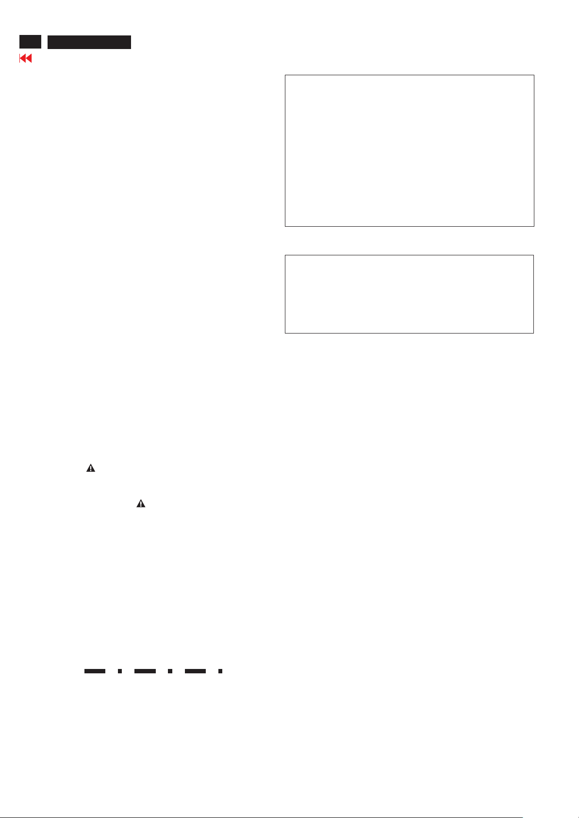
Interface
D-Sub Cable
Length : 1.8 M +/- 50 mm
Connector type : D-sub male with DDC-2B pin assignments.
Pin Assignment:
Horizontal 85 degree(min) (CR=10)
2
Blue connector thumb-operated jackscrews
DVI Cable
The input signals are applied to the display through DVI-D cable.
Length : 1.8 M +/- 50 mm (fixed)
Connector type : DVI-D male with DDC-2B pin assignments
White connector thumb-operated jack screws
Pin Assignment:
Pin No. Description
1 T.M.D.S. data2-
2 T.M.D.S. data2+
3 T.M.D.S. data2 shield
4 No Connect
5 No Connect
6 DDC clock
7 DDC data
8 No Connect
9 T.M.D.S. data1-
10 T.M.D.S. data1+
11 T.M.D.S. data1 shield
12 No Connect
13 No Connect
14 +5V Power
15 Ground(for +5V)– Cable detect
16 Hot plug detect
17 T.M.D.S. data0-
18 T.M.D.S. data0+
19 T.M.D.S. data0 shield
20 No Connect
21 No Connect
22 T.M.D.S clock shield
23 T.M.D.S. clock+
24 T.M.D.S. clock-
Power management
The power consumption and the status indication of the set with
power management function are as follows,
STATUS Horizontal Vertical Power Spec LED
Power On Pulse Pulse < 60 W Green
Off No Pulse No Pulse <1W(Without audio) Amber
According to VESA power saving signal. TCO'03 power saving
requirement EPA energy star requirement (DC power Switch
Off) Power consumption is less 1W (Without audio.)
4
190P5
190P5
Go to cover page
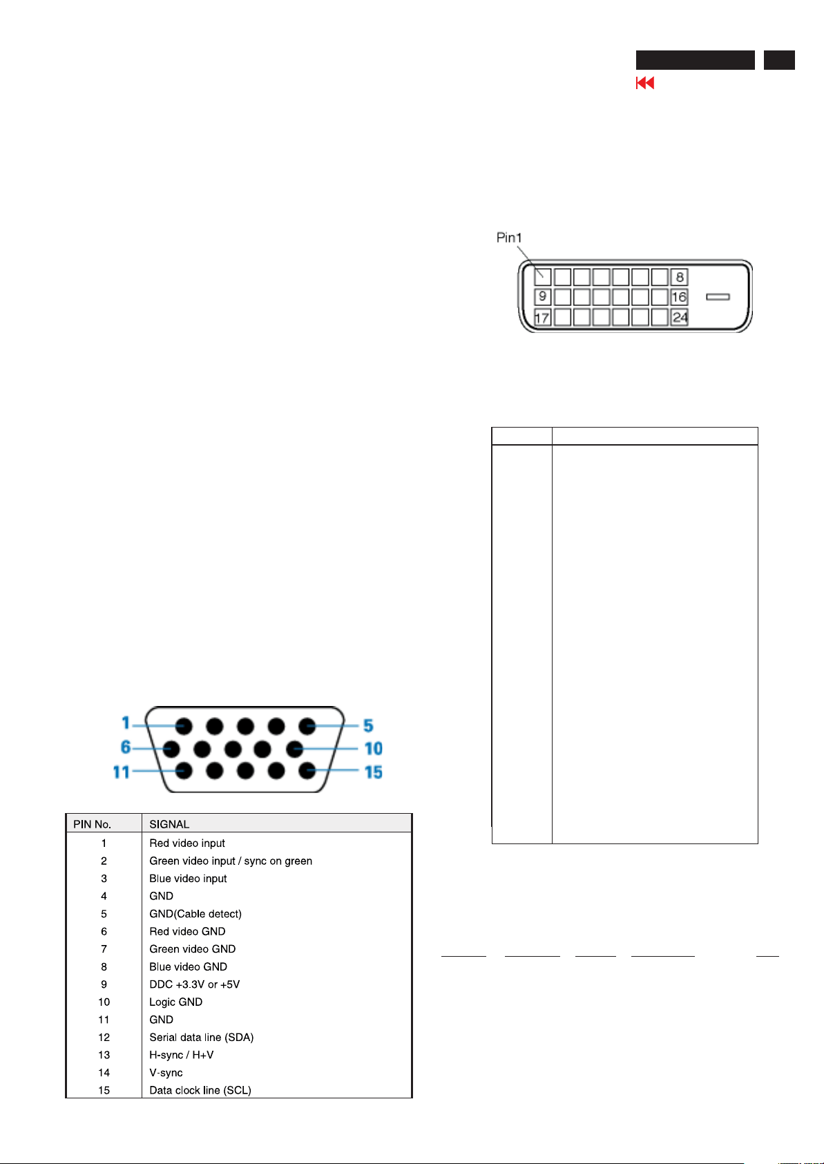
Installation
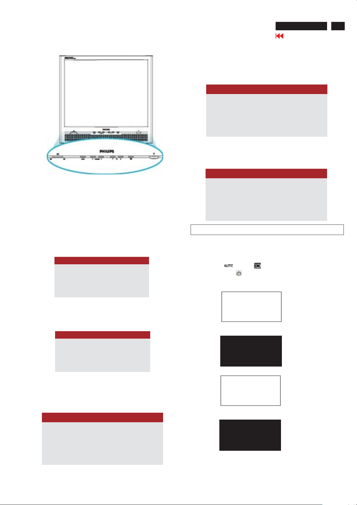
Front View Product Description
UP and DOWN buttons are used when adjusting
the OSD of your monitor.
LEFT and RIGHT buttons, like the UP and
DOWN buttons, are also used in adjusting the
OSD of your monitor.
BRIGHTNESS hotkey. When the UP and DOWN
arrow buttons are pressed, the adjustment
controls for theBRIGHTNESS will show up.
VOLUME hotkey. When the LEFT and RIGHT
VOLUME
arrow buttons are pressed, the adjustment
controls for VOLUME will show up.
OK button which when pressed will take you to
the OSD controls.
Connecting your monitor
1) Plug the cables into connectors.
If you use an Apple Macintosh, you need to connect
the special Mac adapter to one end of the monitor
signal cable.
Rear View
POWER button switches your monitor on.
Automatically adjust the horizontal position,
vertical position, phase and clock setting.
LightFrameTMhotkey for mode-switching
between full-screen mode and multi-window
mode.
1 Kensington anti-thief lock
2 VGA input
3 Earphone jack
4 DVI-D input
5 PC audio input
6 AC power input
2) Connect to PC
(a) Turn off your computer and unplug its power cable.
(b) Connect the monitor signal cable to the video connector on
the back of your computer.
(c) Plug the power cord of your computer and your monitor into
a nearby outlet.
(d) Turn on your computer and monitor. If the monitor displays
an image,installation is complete.
190P5
On Screen Display
190P5
Go to cover page
On-Screen Display
This is a feature in all Philips LCD monitors. It allows an end user to adjust screen performance of the monitors directly through an onscreen instruction window. The user interface provides user-friendliness and ease-of-use when operating the monitor.
Basic and simple instruction on the control keys.
When you press the button on the front control of your monitor, the On-Screen Display (OSD)
Main Controls window will pop up and you can then start making adjustments to your monitor's various
features. Use the or the keys to make your adjustments.
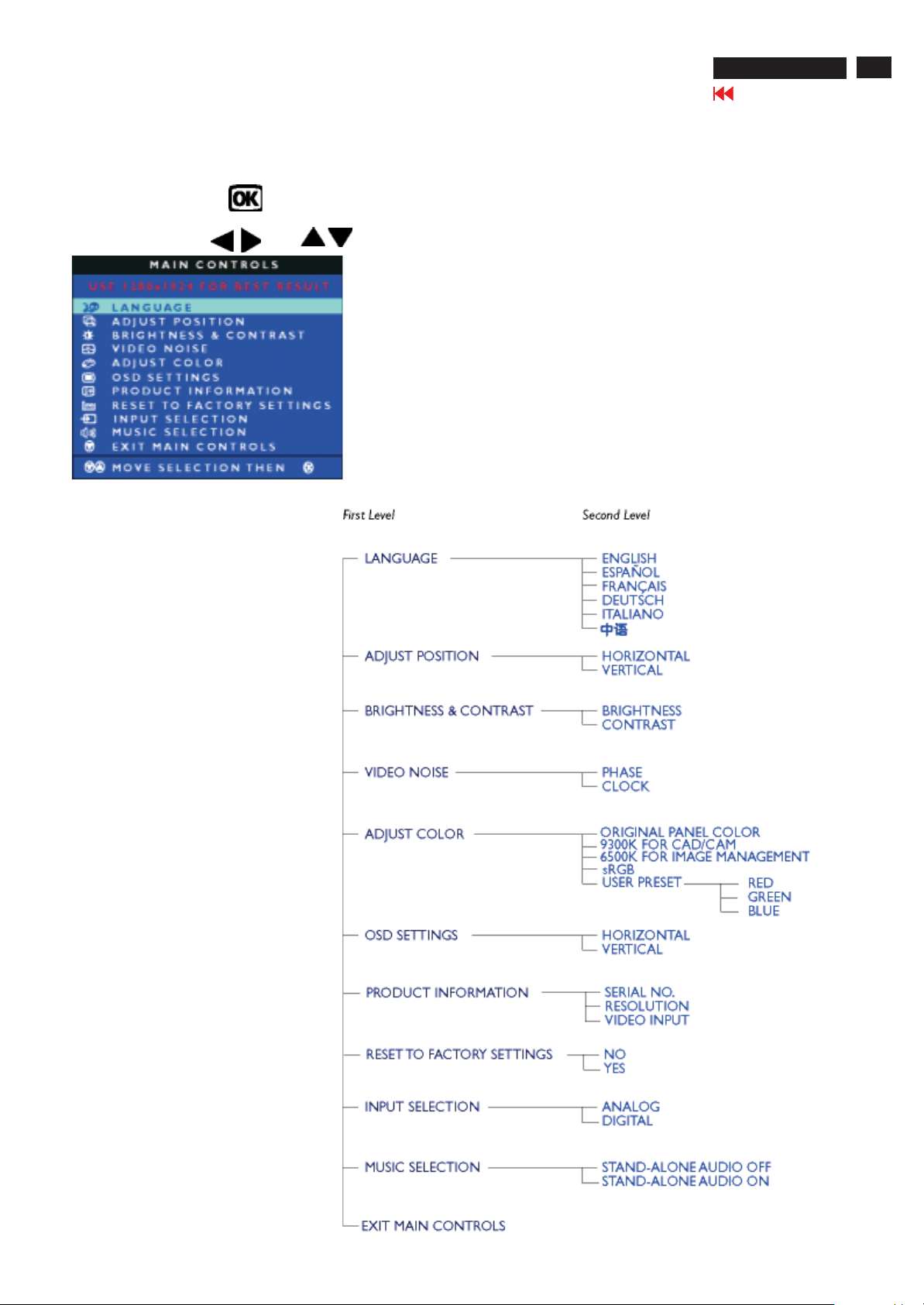
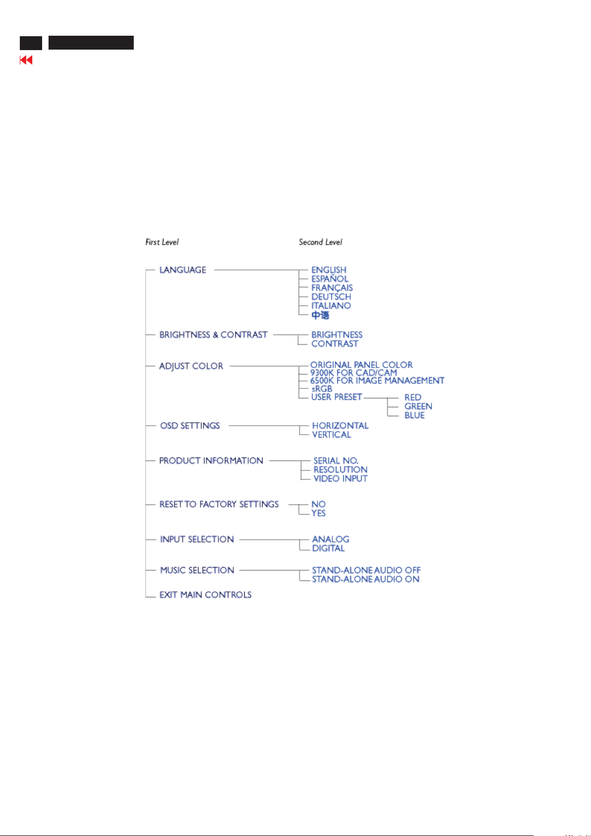
The OSD Tree
Below is an overall view of the structure of
the On-Screen Display. You can use this as
a reference when you want to work your way
around the different adjustments later on.
Analog signal input:
5
6
Go to cover page
Digital signal input:
190P5
On Screen Display
OSD Lock/Unlock, Aging Mode
190P5
Go to cover page
7
Front control panel
Fig. 1
To Lock/Unlock OSD function (User Mode)
CANNOT DISPLAY THIS VIDEO MODE..
This screen warns when the input frequency from the computer is not
a standard video mode or out of the monitor's scanning range.
Please change the display mode of the operating software in the
computer(i.e. Windows) to 1280x 1024@ 60Hz for best display
results.
ATTENTION
CANNOT DISPLAY THIS VIDEO
MODE, CHANGE COMPUTER DISPLAY
INPUT TO 1280X1024@60HZ
WAIT FOR AUTOMATIC ADJUSTMENT
This screen appears when you press the buttons at the
same time . It will disappear when the monitor is properly adjusted.
”AUTO”
ATTENTION
WAITING FOR AUTOMATIC ADJUSTMENT
The OSD function can be locked by pressing "OK" button(1) for more
than 10 seconds, the screen shows following windows for 3 seconds.
Everytime when you press "AUTO" or "OK" button, this message
appears on the screen automatically.
ATTENTION
OSD MAIN CONTROLS LOCKED
Unlock OSD function:
Locked OSD function can be released by pressing"OK" button for
more than 10 seconds again.
Fig. 2
ATTENTION
OSD MAIN CONTROLS UNLOCKED
NO VIDEO INPUT
This screen appears if there is no video signal input. Please check
that the signal cable is properly connected to the video card of PC
and make sure PC is on.
Fig. 3
ATTENTION
Access Aging.. Mode
Step 1: Turn off LCD monitor, and disconnect Interface Cable
Step 2 :
it]+[Press power " " button untill comes out "AGING screen"
Bring up
After 15 seconds, bring up :
After 15 seconds, bring up :
between Monitor and PC.
[Push AUTO " " & OK " " buttons at the same time and hold
] => then release all buttons.
:
AGING...AGI N G ...
AGING...AGI N G ...
After 15 seconds, bring up :
NO VIDEO INPUT
----------
---------repeatly
Connect signal cable again => go back to normal display.
8
Go to cover page
190P5
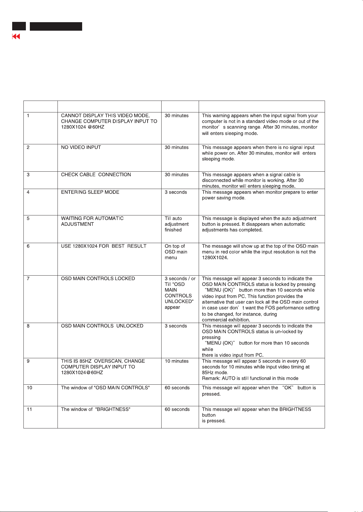
Warning message table
Warning message table
Item Attention Signals Display Time Condition
Front control panel
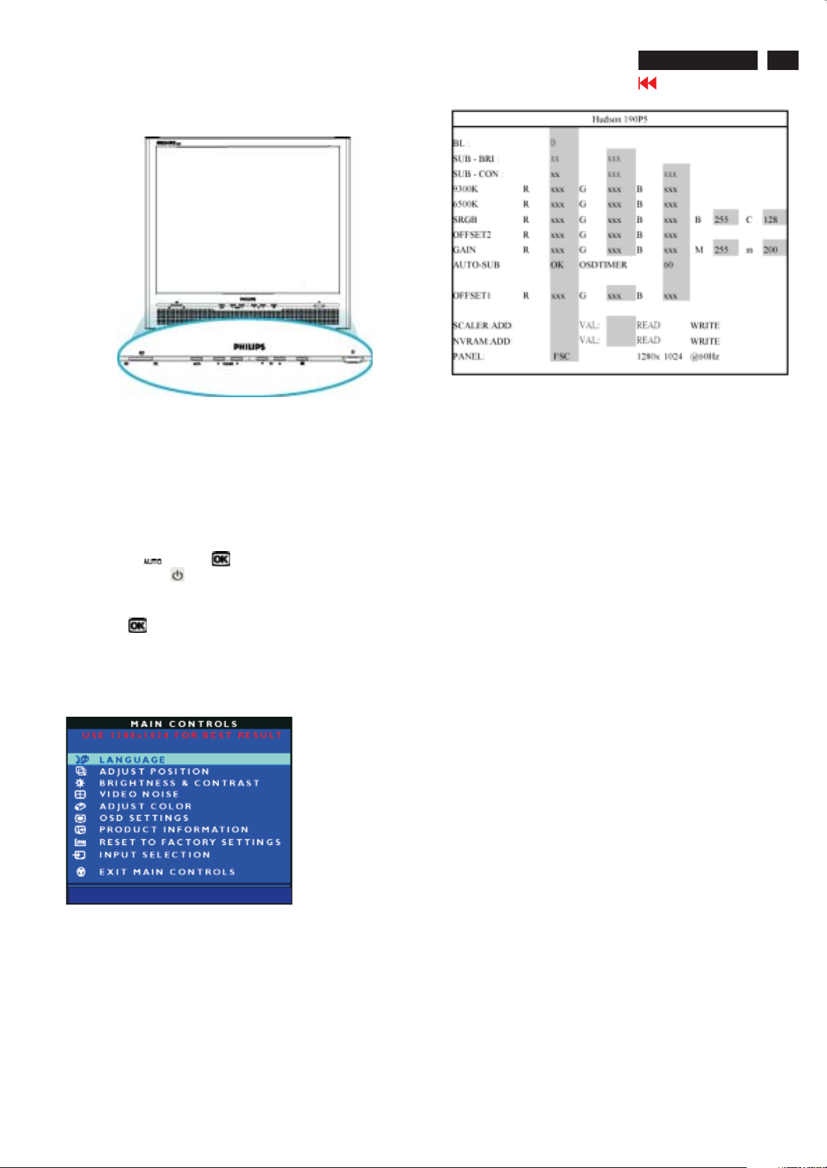
Factory mode
190P5
Go to cover page
9
Fig. 1
Access Factory Mode
How to Get into Factory Mode Menu
Step 1 :
Turn off monitor.
Step 2 :
[Push AUTO " " & OK " " buttons at the same time and hold
it]+[Press power " " button untill comes out "Windows screen"
] => then release all buttons.
Step 3 :
Press OK " " button, bring up Factory mode indication as
shown in Fig 2.
<---Mean:itisnot
1280 x1024
resolution now.
Fig. 3
BL : Black Level value
SUB-BRI : Brightness value range(Min , Max)
SUB-CON : Contrast value range(Min , Mid , Max)
SRGB-B : Brightness of sRGB
SRGB-C : Contrast of sRGB
Gain-m : Minimum value of User Gain
Gain-M : Maximum value of User Gain
AUTO-SUB: To do Auto color function when push
Menu key in white pattern
OSDTIMER : OSD time out control(sec)
SCALER : Read/Write scaler register
NVRAM : Read/Write EEPROM address
Panel : Panel type display (FSC)
Fig. 2
HUDSON 190P5 V016 2003-10-27
<------Factory mode indicator
Factory menu
Cursor can move on gray color area
Hot key function: by pressing "UP" and "DOWN" key
(PS: The OffsetRGB function can be used on reduce or eliminate
snowy noise on the background when the resolution of video signal is
1280 X 1024 vertical 60Hz. Slightly increase or decrease the value
until snowy noise completely disappear.)
simultaneously at User mode (or Factory mode).
SUB CON:SUB CON:
-
Contrast adjustment (Sub-Contrast). Use this menu item to
adjust the contrast gain of pre-amp ranges from 0 to 255.
9300KRGB
6500KRGB
OFFSET R G B
GAIN R G B
Color temperature gain adjustment. Use these menu items
to adjust the RGB gains of pre-amp for different color
temperatures, ranges from 0 to 255.
Sub-Brightness adjustment. Use this menu item to adjust
the brightness level (DC-level) of pre-amp range from 0 to
255.(R/G/B ANALOG DC -level).
R/G/B GAIN adjustment. Use this menu item to adjust
the R/G/B (GAIN) of Amp. range from 0 to 255.(R/G/B
ANALOG GAIN Values).
10
Go to cover page
190P5
Wiring Diagram
330mm
LVDS cable
125 mm
125 mm
Scaler
D_Sub
DVI-I
Embedded
To Key pad
Audio Board
404.2mm
150 mm
AC-DC
AC inlet
Power-Inverter
150 mm

Front view
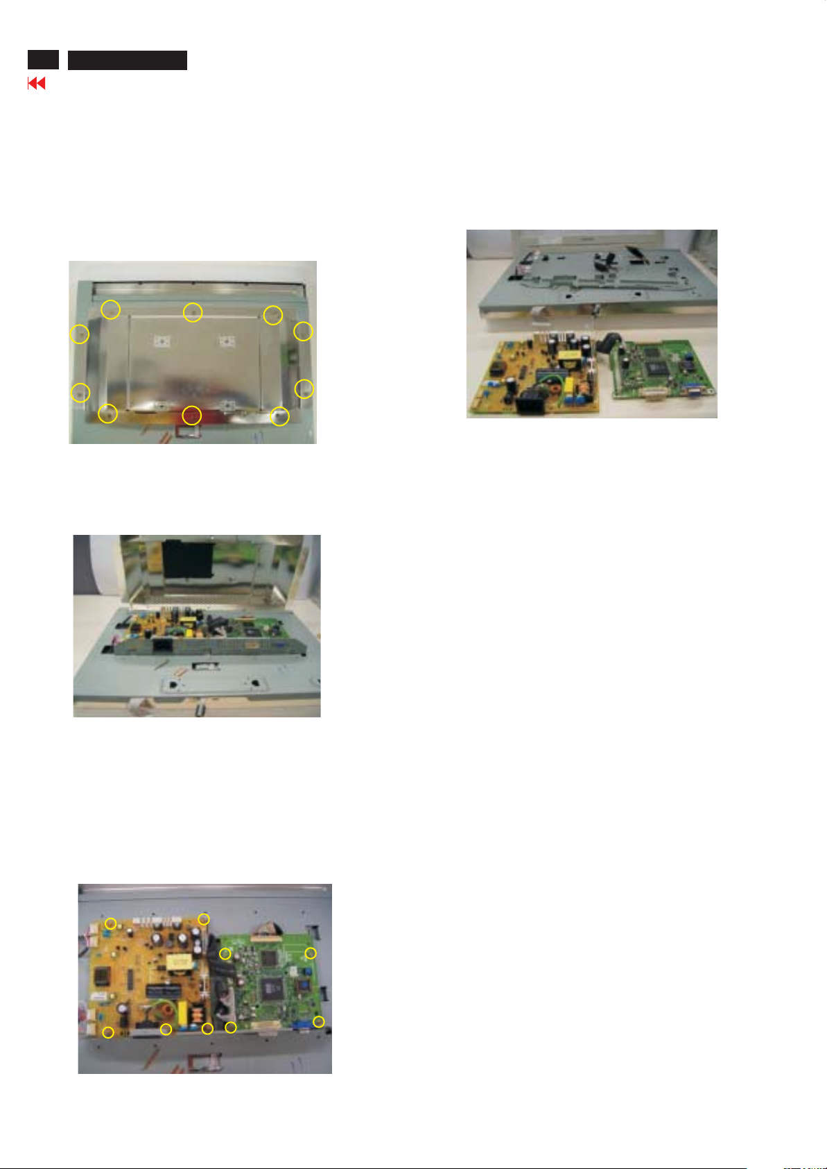
Mechanical Instructions
190P5
Go to cover page
11
Back view
Fig. 1
Fig. 2
=====>
Botton view
=====>
Right and Left view
Step 3.Remove the
- Remove the one screw as shown in Fig, 7.
- Remove the Control board as shown in Fig. 7~8.
Use the thin "I" type screw driver to open the clicks
-
as shown in Fig. 9.
Back cover
=====>
=====>
Fig.5
=====>
Fig.6
Step 1. Remove the base as shown in Fig .3
- Remover the four screws
Step 2. Remove the Front Bezel
- Remove the two screws as shown in Fig. 4
- Use the thin "I" type screw driver to open the clicks
as shown in Fig.5~6.
Control board
Fig.7
Fig. 3
=====>
Fig.8
Fig. 4
=====>
Right and Left view
=====>
Fig.9
12
190P5
Go to cover page
Step 4.Remove the Scaler and Power board
- Remove the 10 screws as shown in Fig. 10 .
- Disconnect DVI and D-SUB hexagonal screws
as shown in Fig. 10.
- Remove the matel frame board as shown in Fig. 11.
Mechanical Instructions
1156 823827714551 TFT-LCD MOD FLC48XWC8V-10(FDT0
==========>
Panel
======>
======>
======>
4 Hexagonal screws
======>
Fig.10
Fig.11
Power
Fig. 13
***************************************************************************
In warranty, it is not allowed to disassembly the LCD panel, even the
backlight unit defect.
Out of warranty, the replacment of backlight unit is a correct way
when the defect is cused by backlight (CCFL,Lamp).
***************************************************************************
Scaler
Step 5. Remove the scaler and power board .
- Remove the 9 screws as shown in Fig. 12.
- Disconnect the 1411,1502 ,1503,1504 and 4 backlight cables
as shown in Fig12 .
- Remove the scaler and power board as shown in Fig13.
======>
1411 to panel
4 backlight cables
======>
1502 to power
1503 to control
1504 to video
Fig. 12
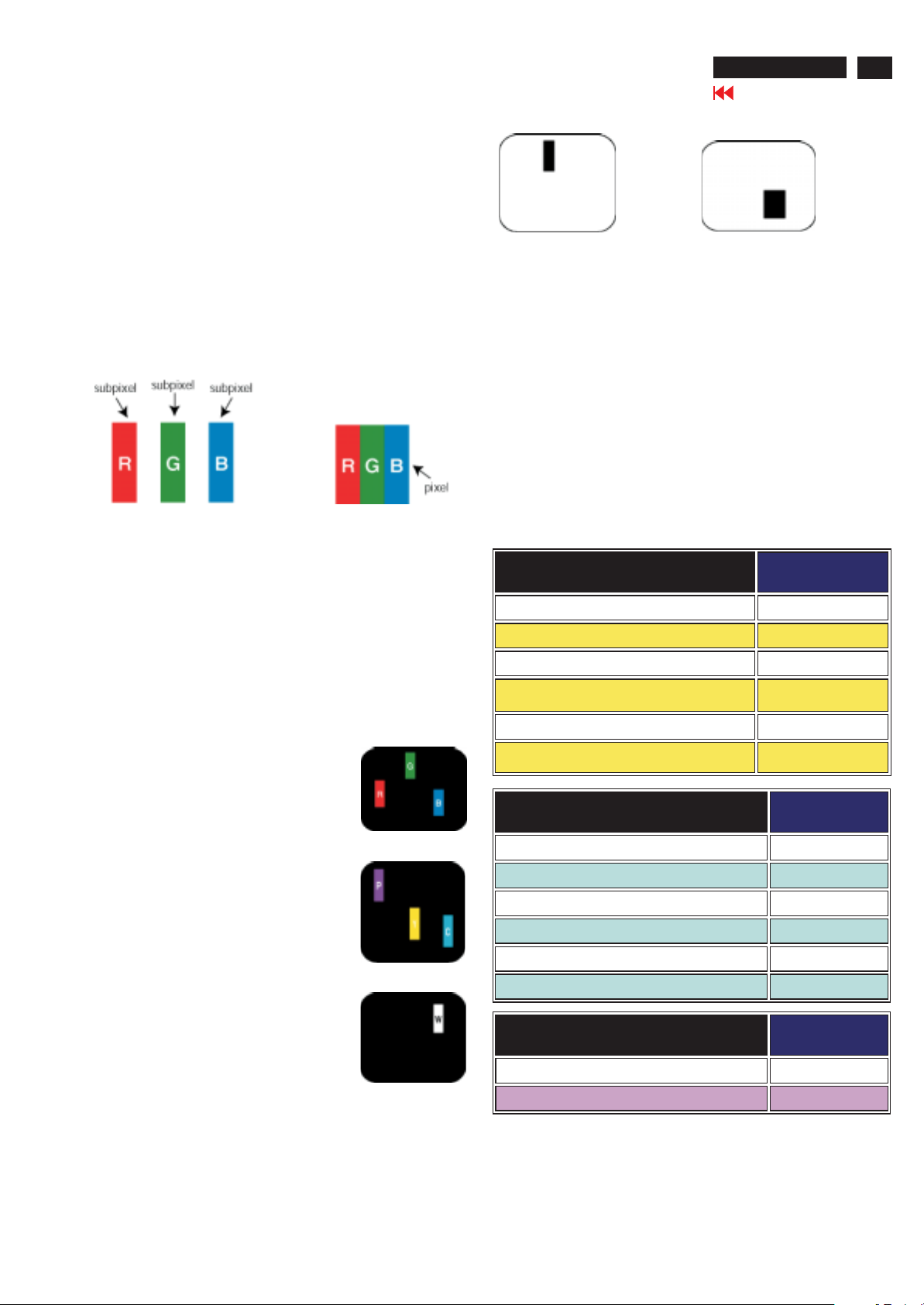
Definition of Pixel Defects
Philips' Flat Panel MonitorsPixel Defect Policy
Philips strives to deliver the highest quality products. We use some of
the industry's most advanced manufacturing processes and practise
stringent quality control. However, pixel or sub pixel defects on the TFT
LCD panels used in flat panel monitors are sometimes unavoidable. No
manufacturer can guarantee that all panels will be free from pixel
defects, but Philips guarantees that any monitor with an unacceptable
number of defects will be repaired or replaced under warranty. This
notice explains the different types of pixel defects and defines
acceptable defect levels for each type. In order to qualify for repair or
replacement under warranty, the number of pixel defects on a TFT LCD
panel must exceed these acceptable levels. For example, no more than
0.0004% of the sub pixels on a 15" XGA monitor may be defective.
Furthermore, Philips sets even higher quality standards for certain types
or combinations of pixel defects that are more noticeable than others.
This policy is valid worldwide.
190P5
13
Go to cover page
One dark sub pixel
Proximity of Pixel Defects
Because pixel and sub pixels defects of the same type that are near to
one another may be more noticeable, Philips also specifies tolerances
for the proximity of pixel defects.
Pixel Defect Tolerances
In order to qualify for repair or replacement due to pixel defects during
the warranty period, a TFT LCD panel in a Philips flat panel monitor
must have pixel or sub pixel defects exceeding the tolerances listed in
the following tables.
Two or three adjacent dark sub pixels
Pixels and Sub pixels
A pixel, or picture element, is composed of three sub pixels in the
primary colors of red, green and blue. Many pixels together form an
image. When all sub pixels of a pixel are lit, the three colored subpixels
together appear as a single white pixel. When all are dark, the three
colored sub pixels together appear as a single black pixel. Other
combinations of lit and dark sub pixels appear as single pixels of other
colors.
Types of Pixel Defects
Pixel and sub pixel defects appear on the screen in different ways.
There are two categories of pixel defects and several types of sub pixel
defects within each category.
Bright Dot Defects appear as pixels or sub pixels that are always lit or
'on'. These are the types of bright dot defects:
-One lit red, green or blue sub pixel
Two adjacent lit sub pixels:
- Red + Blue = Purple
- Red + Green = Yellow
- Green + Blue = Cyan (Light Blue)
BRIGHT DOT DEFECTS
ACCEPTABLE
LEVEL
MODEL 190P5
1 lit subpixel 4 or fewer
2 adjacent lit subpixels 2 or fewer
3 adjacent lit subpixels (one white pixel) 0
Distance between two bright dot defects* 15 mm or more
Total bright dot defects of all types 4 or fewer
BLACK DOT DEFECTS
ACCEPTABLE
LEVEL
MODEL 190P5
1 dark subpixel 6 or fewer
2 adjacent dark subpixels 2 or fewer
3 adjacent dark subpixels 0
Distance between two black dot defects* 15 mm or more
-Three adjacent lit sub pixels (one white pixel)
Black Dot Defects
Appear as pixels or sub pixels that are always dark or 'off'. These are
the types of black dot defects:
Total black dot defects of all types 6 or fewer
TOTAL DOT DEFECTS
ACCEPTABLE
LEVEL
MODEL 190P5
Total bright or black dot defects of all types 6 or fewer
Note: 1 or 2 adjacent sub pixel defects = 1 dot defect
All Philips monitors are ISO13406-2 Compliant
14
190P5
Go to cover page
Electrical Instructions
1.2.General points
1.1 During the test and measuring, supply a distortion free AC
mains voltage to the apparatus via an isolated transformer
with low internal resistance.
1.2 All measurements mentioned hereafter are carried out at a
normal mains voltage (90 - 132 VAC for USAversion, 195 264 VAC for EUROPEAN version, or 90 - 264 VAC for the
model with full range power supply, unless otherwise
stated.)
1.3 All voltages are to be measured or applied with respect to
ground, unless otherwise stated.
Note: don't use heat-sink as ground.
1.4 The test has to be done on a complete set including LCD
panel after 30 minutes warm-up at least in a room with
temperature of 25 +/- 5 degree C.
1.5 All values mentioned in these test instruction are only
applicable of a well aligned apparatus, with correct signal.
1.6 The letters symbols (B) and (S) placed behind the test
instruction denotes
(B): carried out 100% inspection at assembly line
(S): carried out test by sampling
1.7 The white balance (color temperature) has to be tested in
subdued lighted room.
1.8 Repetitive power on / off cycle are allowed except it should
be avoided within 6 sec.
Input signal
2.1 Signal type
2.1.1 Video signal input
Signal source: pattern generator format as
attachment.(Table 1 to 34)
Reference generator: QuantumData 802G
The input signals can be applied via VESA analog:
The video input consists of red, green, and blue signals. The
video signals are analog levels, where 0V corresponds to
black and 700mV is the maximum signal amplitude. Input
impedance of video pins is 75 ohm +/- 1%.
2.1.2 Sync signal input
The capability of sync signal inputs shall include separate
sync, composite sync and sync
on green. input impedance: 2k2 ohms The signals are
defined as follow:
PRESET VIDEO RESOLUTION
# Resolution H-
Frequency
1 640X350 31.5K 25.175 70Hz IBM VGA 10h
2 720X400 31.5K 28.322 70Hz IBM VGA 3h
3 640X480 31.5K 25.175 60Hz
4 640X480 35.0K 30.24 67Hz
5 640X480 37.9K 31.5 72Hz
6 640X480 37.5K 31.501 75Hz
7 640X480 43.3K 36 85Hz
8 800X600 35.2K 36 56Hz
9 800X600 37.9K 40 60Hz
10 800X600 48.1K 50 72Hz
11 800X600 46.9K 49.498 75Hz
12 800X600 53.7K 56.251 85Hz
13 832X624 49.7K/ 57.28 75Hz MAC
14 960X720 44.76K 57.58 60Hz
15 960X720 56.4K 72.42 75Hz
16 1024X768 48.4K 65 60Hz
17 1024X768 56.5K 75 70Hz
18 1024X768 60.0K 78.75 75Hz
19 1024X768 61.1K 83.096 76Hz IBM XGA-2
20 1024X768 68.7K 94.5 85Hz
21 1152X864 54.0K 79.9 60Hz Non-VESA
22 1152X864 63.9K 94.5 70Hz Non-VESA
23 1152X864 67.5K 108 75Hz
24 1152X870 68.7K 100 75Hz MAC
25 1152X900 61.8K 92.94 66Hz SUN Mode IV
26 1152X900 71.8K 108 76Hz SUN Mode II
27 1280X960 60.0K 108 60Hz
28 1280X960 75.0K 129.895 75Hz Non-VESA
29 1280X1024 64.0K 108 60Hz
30 1280X1024 71.7K 117 67Hz SUN Mode V
31 1280X1024 76.0K 130.223 72Hz DOS/V
32 1280X1024 80.0K 135 75Hz
33 1280X1024 81.1K 135.008 76Hz SUN Mode I
Pixel rate V-
Frequency
Comment
Separate sync TTL level, Positive/Negative
Composite sync TTL level, Positive/Negative
Sync on green H-sync TTL level, Positive/Negative
Signal source: pattern generator format as attachment
2.2 Input signal mode
Pre-set 34 modes
Reference generator: QuantumData 802G
Electrical Instructions
2.3 Allowed 85 Hz overscan signal mode specified
Once the signal input of PC is 85Hz, this monitor is able to
display at least for 10 minutes. An attention signal appears
and shows This is 85Hz overscan for 5 seconds, change
computer display input to 1280 x1024 @ 60 Hz .
Dot rate (MHz) H. Freq (KHz) Mode Resolution V. Freq (Hz)
36.000 43.269 VESA 640 * 480 85.008
5 56.250 53.674 VESA 800 * 600 85.061
94.500 68.677 VESA 1024 * 768 84.997
3. POWER SUPPLY
Setup the AC I/P at 90VAC, add 2.4Aloading to
C2124 and DC O/P voltage is 12V +/- 1.2V; 1A
loading to C2004 and DC O/P voltage is 3.3V +/-
0.165V.Or,1.5A loading to C2136 and DC O/P
voltage is 5V +/- 0.25(S)
4. Display Adjustment
4.1 Access to factory mode.
190P5
Go to cover page
15
4.2 Auto color adjustment (B)
4.3 Adjustment of WHITE-D (B)
Apply a 48.36kHz/60Hz signal with 'Black& white'
pattern, set brightness control at 100%, and contrast
control at 50%.
Adjust the R. G. B offset, and gain to calibrate the color
smoothly and 64-gray level distinguishable.
Check all pre-setting 34 modes.
Apply a 1024*768 / 60Hz signal with white pattern, set
brightness control at 100%,
and contrast control at 50%. Adjust the R, G, B Sub-Gain,
for the screen central, the 1931
CIE chromaticity (X, Y) co-ordinates shall be;
9300°K 6500°K sRGB
x (center) 0.283 ± 0.020 0.313 ± 0.020 0.313 ± 0.020
y (center) 0.297 ± 0.020 0.329 ± 0.020 0.329 ± 0.020
Use Minolta CA-110 for color coordinates and luminance
check.
Luminance is > 200 Nits in the center of the screen when
brightness at 100% and Contrast set to 100% with original
color.
4.4 EEPROM presetting (B)
After finishing all the adjustment, set:
Brightness control to 100%
Contrast control to 50%
Audio 50%
Audio, stand-alone, default = off
OSD position at middle of screen
'COLOR ADJUST' to 6500K color.
4.5 When adjustment is finished, monitor should be set to
6500K.
16
Go to cover page
190P5
190P5
Function Block Diagram
Scalar Board
12V
D
5V
C
3.3V
LVDS ConnectorLVDS Connector
Pacific
Pacific
1SB
1SB
TTL RGB
TTL RGBTTL RGB
C
O
N
T
R
O
L
Audio
GM5120
GM5120GM5120
TMDS ADC
TMDSTMDS ADCADC
MCUGPIO
MCUMCUGPIOGPIO
Flash
Flash
Rom
Rom
DSUBDSUBDVI-DDVI-D
Schematic diagram(Scaler)
190P5
Go to cover page
17
A
B
C
D
All rights reserved. Reproduction in whole or in parts
is prohibited without the written consent of the copyright
owner.
E
F
G
H
gedeeltelijk, is niet toegestaan dan met schriftelijke
toestemming van de auteursrechthebbende.
Alle rechten voorbehouden. Verveelvuldiging, geheel of
I
25
1
+3.3V
A
DVI_CABLE
3210
10K
I108
3209
47K
3204
100R
B
C
D
E
F
EXCEPT 1201,1203 WERE CHIP COMPONENTS.
3
4
6
7
2345
+3.3V
1201
26
3208
8
16
24
7
15
23
6
14
5
22
13
21
4
12
20
3
11
19
2
10
18
1
9
17
25
ISPSDA
ISPSCL
3223
100R
3225
100R
RXC-
DDCSDA_D
RXC+
DDCSCL_D
5201
100MHZ
RX2+
RX1+
RX0+
RX2RX1RX0-
3216
100R
3217
2218
2210
322110K
10K 3222
2216330p
330p 2217
100R
DDCSDA
3224
DDCSCL
33p
10R
100n
2233
100R3226
100R
2219
3206
100R
3207
100R
3227
100n
ASDA
ASCL
2K2
220p
10K
3230
HIN
VIN
6201
3202
2211
I252
10K
I254
10K
330p
3228
I253
2K2
3203
2212
3215
5
SDA
I255
I256
10K
I109
330p
I110
+3.3V
6220
8
VSS
4
16
11
12
13
14
15
17
I144
2209
100n
5
SDA
3239
100R
3240
100R
BAT42W
VCC
1203
1216-004-15S-AAC
6
1
7
2
8
3
9
4
10
5
VSIN
HSIN
4
M24C02
E0
E1
E2
SCL
WC_
8
VCC
7203
VSS
7202
DVISDA
DVISCL
1
2
3
6
7
5202
100MHZ
3205
100R
E0
E1
E2
SCL
WC_
I251
1
2
3
6
7
3231
I258
I262
3214
3213
I257
6221
10R
2221
10K
I145
10K
BAS32L
6222
100n
+3.3V
3229
6223
R
G
B
47K
3233
3235
3237
3238
10K
+12VCC
DDC
+3.3V
1K
3219
10K
3201
6202
3232
100R
75R75R
3234
100R
3236
100R
75R
DSUB_CABLE
I146
6210
6215
I147
BZX84-C5V1
I259
2226
NI
I260
2228
NI
I261
2230
NI
12p
12p
12p
6203
2225
10n
2227
10n
2229
10n
2205
100n
2201
RIN
GIN
BIN
8
9
101
11
12
6789
SCALER PCB
SB: 59371 x4
PB: 59381
100n
6204
6211
6216
VS
HS
HSIN
VSIN
2202 100n
0R05
3218
0R05
3220
2206
NI
NI
6205
100n
I266
6212
6217
100n2203
VIN HIN DDCSCL DDCSDABRG
1
3
5
9
11
13
2207
6206
7211
74LVC14APW-T
14
GND
VCC
RXC+RX0+RX1+RX2+
100n
6213
RXC-RX0-RX1-RX2-
6218
6207
2213
100n
2
3211
I267
4
6
8
10
12
7
100R
3212
100R
NI
NI
2231
2232
33p
330p
2208
+3.3V
6208
HS
VS
100n
DDCSCL_D
6214
DDCSDA_D
6219
6209
A
B
C
D
E
F
1201 A2
1203 D4
2201 C6
2202 C6
2203 C7
2205 A6
2206 A7
2207 A8
2208 A9
2209 A3
2210 B2
2211 B3
2212 A3
2213 D8
2216 D2
2217 D2
2218 F2
2219 F3
2221 F4
2225 D5
2226 E5
2227 E5
2228 E5
2229 F5
2230 F5
2231 E9
2232 E9
2233 C3
3201 C5
3202 A3
3203 A3
3204 A1
3205 E4
3206 A3
3207 B3
3208 A2
3209 A1
3210 A1
3211 E8
3212 E8
3213 B4
3214 A4
3215 C3
3216 D2
3217 E2
3218 D7
3219 A5
3220 E7
3221 C2
3222 C2
3223 E2
3224 E2
3225 E2
3226 E2
3227 F3
3228 F3
3229 F4
3230 D3
3231 E4
3232 D5
3233 E5
3234 E5
3235 E5
3236 E5
3237 F5
3238 F5
3239 B4
3240 B4
5201 B2
5202 E4
6201 A3
6202 C5
6203 D5
6204 D6
6205 D7
6206 D8
13
6207 D8
6208 D9
6209 D9
6210 B5
6211 B6
6212 B7
6213 B8
6214 B9
6215 C5
6216 B6
6217 B7
6218 B8
6219 B9
6220 C3
6221 D4
6222 D4
6223 B4
7202 C4
7203 A4
7211 D8
I108 A1
I109 A3
I110 B3
I144 A4
I145 A4
I146 A5
I147 C5
I251 C4
I252 D3
I253 D3
I254 D3
I255 F3
I256 F3
I257 E4
I258 F4
I259 D5
I260 E5
I261 F5
I262 D4
I266 E7
I267 E8
A
B
C
D
E
F
G
H
I
1 2345
CHN SETNAME SH5 ( HUDSON-190P5 )
CLASS_NO
6
TYT12-
789
--------
1
DSUB/DVI
J
9332153702156219
9332153702156218
9332153702156217
9332153702156216
12p
10K
3213 212211805669
2230 319801631290
3201 232270260103
10K
319802190030
0R05
3218
3219 232270461002
4
1K
0R05
3220 319802190030
3230 212211805669
10K
933137390215
BZX84-C5V1
6203 933215370215
6202
319801631290
Reserved
100n
2201 223878615649
2202 223878615649
Ref Des
100n
100n
2203 223878615649
2205 223878615649
223878615649
100n
100n
2206 223878615649
2207
100n
100n
12p
2208 223878615649
2226 319801631290
2228
12p
1
9332153702156207
933215370215
9332153702156205
6204 933215370215
6206
5
9332153702156208
9332153702156210
933215370215
6209
9332153702156211
6212 933215370215
6213 933215370215
933215370215
6214 933215370215
6215
2003-11-28 3
Alger Huang
NAME
7
82
190P5ES/00
SUPERS.
******** 2003-11-28
CHECKMGr DATE
9
51
1063 12
3138 158 5759
13010 *** A3
C
KONINKLIJKE PHILIPS ELECTRONICS N.V. 2000
11
13
J
18
190P5
190P5
Go to cover page
Schematic Diagram (Scaler)
All rights reserved. Reproduction in whole or in parts
owner.
is prohibited without the written consent of the copyright
G
A
B
C
D
E
1
1
32
2
4
3
A
3361
+3.3V
13
14
15
17
18
19
20
21
24
31
22
5310
100MHZ
DQ0
DQ1
DQ2
DQ3
DQ4
DQ5
DQ6
DQ7
10K
OE
WE
CE
3374
+3.3V
B
C
F
D
DATA0
DATA1
DATA2
DATA3
DATA4
DATA5
DATA6
DATA7
ROM_OE
M29W_WE
3360
+3.3V
10K
2320
10K
I207
100n
30
32
NC1
VCC
(1310)
7310
M29W010B-90K1
VSS
NC0
16
1
A0
A1
A2
A3
A4
A5
A6
A7
A8
A9
A10
A11
A12
A13
A14
A15
A16
E
56
456789
+3.3V
3363
3366
10K
10K
10K
33643367
NI
ADDR0
ADDR1
ADDR2
ADDR3
ADDR4
ADDR5
ADDR6
ADDR7
ADDR8
ADDR9
ADDR10
ADDR11
ADDR12
ADDR13
ADDR14
ADDR15
BANK
10K
+3.3V
10K
3362
NI
12
11
10
27
26
23
25
28
29
NI
9
8
7
6
5
4
3
2
10K
3365
24C16_WP
IICSCL
IICSDA
+3.3V
2321
3369
NI
7
100n
10K
3368
4K7
3370
4K7
3371
3372
100R
3373
100R
10K
8
(1311)
7311
M24C16-WBN6
8
VCC
7
WC
6
SCL
5
SDA
Ref Des Reserved
3362 232270260103
3363
3364 232270260103
3369 232270260103
9
1
E0
2
E1
3
E2
4
VSS
10K
232270260103
10K
10K
10K
10
SCALER PCB
SB: 59371 x4
PB: 59381
5311
+3.3V
100MHZ
TXD
RXD
3375
11
47K
I208
+3.3V+3.3V
3376
47K
1305
JFE63173
1
2
3
4
RS232 PORT
12
A
B
C
D
E
1305 C9
2320 B2
2321 B5
3360 D2
3361 D2
3362 B3
3363 B4
3364 B4
3365 E3
3366 E4
3367 E4
3368 B5
3369 C5
3370 B6
3371 B6
3372 C6
3373 C6
3374 E2
3375 B9
3376 B9
5310 A2
5311 C8
7310 C3
7311 C7
I207 A3
I208 C9
13
A
B
C
D
E
F
G
H
gedeeltelijk, is niet toegestaan dan met schriftelijke
toestemming van de auteursrechthebbende.
Alle rechten voorbehouden. Verveelvuldiging, geheel of
I
J
H
EXCEPT 1305,7311 WERE CHIP COMPONENTS.
34512
67
CHN SETNAME SH5 ( HUDSON-190P5 )
TYT12-
CLASS_NO
89
I
--------
1
ROM
2003-11-28 3
190P5ES/00
Alger Huang
NAME
CHECKMGr DATE
1
34 12
5
6
7
8
SUPERS.
******** 2003-11-28
9
10
52
3138 158 5759
13010 *** A3
C
KONINKLIJKE PHILIPS ELECTRONICS N.V. 2000
11
132
J
Schematic diagram(Scaler)
190P5
Go to cover page
19
1234
113
PPWR
114
PBIAS
152
TCLK
151
XTAL
206
GPIO20
207
GPIO19
208
GPIO18
1
GPIO17
205
GPIO16_HFS
204
GPIO22_HCLK
6
DDC_SCL
7
DDC_SDA
5
RESETn
4
GPIO21_IRQn
171
RED+
170
RED-
167
GREEN+
166
GREEN-
163
BLUE+
162
BLUE-
137
HSYNC
136
VSYNC
159
ADC_TEST
174
REXT
194
RXC+
195
RXC-
191
RX0+
192
RX0-
185
RX1+
186
RX1-
179
RX2+
180
RX2-
39
GPIO8_IRQINn
50
GPIO11
47
GPIO7
46
GPIO6_TCON_SHC
43
GPIO3_TIMER1
42
GPIO2_PWM2
41
GPIO1_PWM1
40
GPIO0_PWM0
8
ROM_ADDR15
9
ROM_ADDR14
10
ROM_ADDR13
11
ROM_ADDR12
12
ROM_ADDR11
13
ROM_ADDR10
14
ROM_ADDR9
15
ROM_ADDR8
16
ROM_ADDR7
17
ROM_ADDR6
18
ROM_ADDR5
19
ROM_ADDR4
22
ROM_ADDR3
23
ROM_ADDR2
24
ROM_ADDR1
25
ROM_ADDR0
28
ROM_DATA7
29
ROM_DATA6
30
ROM_DATA5
31
ROM_DATA4
32
ROM_DATA3
33
ROM_DATA2
34
ROM_DATA1
35
ROM_DATA0
36
ROM_OEn
3
/ GPIO14
/ GPIO15
/ ROM_WEn
/ TCON_TDIV
3
+3.3_A
173
181
AVDD_IMB
AVDD_RX2
AGND_IMB
AGND_RX2
175
178
2301
22n
4p7
14M31818HZ
2317
1302
DVI_CABLE
DSUB_CABLE
BANK
K_LF
HS
VS
3303
3307
2309
10K
10K
2302
ISPSCL
ISPSDA
10n2307
10n2308
10n
2
+3.3_A
4p7
LF_PWR
LF_RSTN
DVISDA
DVISCL
DDC
RIN
GIN
BIN
3306
2M
RXC+
RXCRX0+
RX0RX1+
RX1RX2+
RX2-
MINTN
M29W_WE
K_LEFT
K_RIGHT
K_OK
K_DOWN
K_UP
ADDR15
ADDR14
ADDR13
ADDR12
ADDR11
ADDR10
ADDR9
ADDR8
ADDR7
ADDR6
ADDR5
ADDR4
ADDR3
ADDR2
ADDR1
ADDR0
DATA7
DATA6
DATA5
DATA4
DATA3
DATA2
DATA1
DATA0
ROM_OE
I126
I127
I124
I125
I120
I121
I122
I123
I115
I116
I117
I118
I130
I119
I107
I113
I114
I099
I100
I101
I102
I103
I104
I105
I106
I074
I075
I076
I077
I078
I079
I081
I082
I083
I084
I085
I086
I087
I088
I089
I090
I091
I092
I093
I094
I095
I096
I097
I098
U8
1
+3.3_A
7304
100n
A
2316
OUT
GND
A
B
B
I128
3305
1
VDD
2
3
SA56616-28
2311 1n
2312
10R
CD
5
NC
4
1n
1n2360
C C
Treat R/G/B as differential pair
3308
C
D
+3.3_A
D
All rights reserved. Reproduction in whole or in parts
is prohibited without the written consent of the copyright
E
F
E
+3.3_A
3309
3310
2364
2359
VOLUME
100R
100R
100R
1K
3304
1n2361
1n2362
1n2363
1n
1n
I111
1n
2355
F
H
gedeeltelijk, is niet toegestaan dan met schriftelijke
toestemming van de auteursrechthebbende. owner.
Alle rechten voorbehouden. Verveelvuldiging, geheel of
G G
I
Ref Des Reserved
1
2314 202055294503
1p
3301 212211805972
0R
4301 313815131961
R
2
H
J
4 12
+2.5_A
199
182
193
187
196
AVDD_RX0
AVDD_RX1
AVDD_RXC
AGND_RXC
AGND_RX0
AGND_RX1
190
184
197
160
164
168
172
AVDD_RED
AVDD_BLUE
AVDD_GREEN
AGND_BLUE
SGND_ADC
AGND_ADC
157
158
161
165
AVDD_ADC
AGND_GREEN
146
150
141
AVDD_RPLL
AVDD_SDDS
AVDD_DDDS
AVSS_RPLL
AVSS_DDDS
AGND_RED
169
145
149
176
VDD_RX1_2.5
VDD_RX2_2.5
VDD_RXPLL_2.5
AVSS_SDDS
AGND_RXPLL
177
198
140
EXCEPT 4301 WERE CHIP COMPONENTS.
4
56789
56
+2.5_D
26
88
155
134
188
VDD_RX0_2.5
gm5125-BD
GND_RX0
GND_RX1
GND_RX2
189
183
Heatsink
4301
12
203
153
CVDD_2.5_3
AVDD1_ADC_2.5
AVDD2_ADC_2.5
7301
CVSS4
GND1_ADC
GND2_ADC
156
154
202
R
5
CVDD_2.5_1
CVDD_2.5_2
CVSS2
CVSS3
133
135
148
VDD_RPLL
CVDD_2.5_0
CVSS0
CVSS1
27
89
139
144
VDD_SDDS
VDD_DDDS
VSS_SDDS
VSS_RPLL
VSS_DDDS
143
147
138
6
129
RVDD8
111
RVDD7
RVSS8
130
112
RVSS7
+3.3_D
53
RVDD367RVDD481RVDD597RVDD6
37
20
RVDD2
38
7
2
DCLK_TCON_OCLK
RVDD1
RVDD0
DVS_TCON_FSYNC
DHS_TCON_LP
DEN_TCON_ECLK
PD47_OB7
PD46_OB6
PD45_OB5
PD44_OB4
PD43_OB3
PD42_OB2
PD41_OB1
PD40_OB0
PD39_OG7
PD38_OG6
PD37_OG5
PD36_OG4
PD35_OG3
PD34_OG2
PD33_OG1
PD32_OD0
PD31_OR7
PD30_OR6
PD29_OR5
PD28_OR4
PD27_OR3
PD26_OR2
PD25_OR1
PD24_OR0
PD23_EB7
PD22_EB6
PD21_EB5
PD20_EB4
PD19_EB3
PD18_EB2
PD17_EB1
PD16_EB0
PD15_EG7
PD14_EG6
PD13_EG5
PD12_EG4
PD11_EG3
PD10_EG2
TCON_OSP
TCON_OPOL
TCON_OINV
TCON_ESP
TCON_EPOL
TCON_EINV
TCON_RSP2
TCON_RSP3
TCON_RCLK
GPIO10_TCON_ROE3
GPIO9_TCON_ROE2
TCON_ROE
GPIO4_UART_D1
GPIO5_UART_D0
NVRAM_SCL /
NVRAM_SDA /
RESERVED1
RESERVED0
RVSS254RVSS368RVSS482RVSS598RVSS6
RVSS021RVSS1
3
7
8
I070
DVS_FSYNC
I071
DHS_LP
3302 51R
I072
110
109
3313
108
107
106
105
104
103
102
101
100
99
96
95
94
93
92
91
90
87
86
85
84
83
I001
B7
80
I002
B6
79
I003
B5
78
I004
B4
77
I005
B3
76
I006
B2
75
I007
B1
74
I008
B0
73
I009
G7
72
I010
G6
71
I011
G5
70
I012
G4
69
I013
G3
66
I014
G2
65
I015
G1
64
I016
G0
63
I017
R7
62
I018
R6
61
I019
R5
60
I020
R4
59
I021
R3
58
I022
R2
57
I023
R1
56
I024
R0
55
I056
GPO0_BL_CTL
I057I080
GPO2_MW_LED
I059
LED_O
I060
I061
I062
I063
24C16_WP
I112
I064
49
I065
48
I066
44
45
52
51
201
200
142
132
131
NAME
RXD
I067
TXD
I068
IICSCL
I069
IICSDA
2369100n
TYT12-
CHN SETNAME SH5 ( HUDSON-190P5 )
CLASS_NO
2003-11-28 3
Alger Huang
PD9_EG1
PD8_EG0
PD7_ER7
PD6_ER6
PD5_ER5
PD4_ER4
PD3_ER3
PD2_ER2
PD1_ER1
PD0_ER0
GPIO13
GPIO12
CLKOUT
NC1
NC0
118
117
116
115
119
120
121
122
123
124
125
126
127
128
CLKH
I073
10K
2314
DE
LED_B
+3.3_A
2371100n
100n 2370
CHECKMGr DATE
9
3328 47R
B3
1
B2
2
B1
3
B0
45
1p
3329
4
B4
3
B5
2
B6
1
B7
3327 47R
1
G3
G2
2
3
G1
G0
45
+3.3V
+3.3V
3311
10K 3312
10K
SHUTDOWN
PANEL_PWR_CTL
K_AUTO
K_PWR
1n
1n
2353
2354
2373100n
2374100n
100n 2372
100n 2375
2377100n
100n 2376
SCALER
190P5ES/00
SUPERS.
******** 2003-11-28
9
R
R
R
R
47R
R
R
R
R
R
R
R
R
AME8815AEGT250
AME8815AEGT250
2310
100n 2378
100n 2379
8
7
6
5
6
7
8
8
7
6
7303
1
1
100n
100n 2380
10
I049
Vi
7302
Vi
10
I025
I026
I027
I028
I033
I034
I035
I036
I041
I042
I043
I044
GND
GND
MT1
MT1
2387
100n
4
ADJ
2
4
ADJ
2
OB3
OB2
OB1
OB0
OB4
OB5
OB6
OB7
OG3
OG2
OG1
OG0
Vo
Vo
+3.3_D
100n 2388
10 11 12
11
3322
R4
R5
R6
R7
47R
45
R
3
R
2
R
1
R
I029
OR4
I030
OR5
6
I031
OR6
7
I032
OR7
8
13
A
SCALER PCB
3325
G4
G5
G6
G7
R3
R2
R1
R0
47R
45
R
3
R
2
R
1
R
47R3324
R
1
R
2
R
3
R
45
SB: 59371 x4
I037
OG4
I038
OG5
6
I039
OG6
7
I040
OG7
8
OR3
I045
8
OR2
I046
7
OR1
I047
6
OR0
I048
PB: 59381
B
D
E
5304
100MHZ
5303
100MHZ
5305
3
100MHZ
I053
0R
3301
NI
I054
5306
3
100MHZ
2390100n
100n 2389
100n 2391
53
C
I050
+3.3_A
47u
2304
I051
+3.3_D
47u
2303
I052
+2.5_A
47u
2305
+2.5_A
I055
+2.5_D
47u
100n 2392
2393100n
2394
100n
2306
2396100n
100n 2395
100n 2397
100n 2398
100n 2365
+2.5_D
2381
100n
3138 158 5759
13010 ***
KONINKLIJKE PHILIPS ELECTRONICS N.V. 2000
118
12
100n 2366
100n 2382
100n 2367
100n 2383
+2.5_D
100n 2368
100n 2384
1
100n 2385
13
100n 2386
--------
F
GG
H
I
J
A3
A
B
C
D
E
F
H
1302 A2
2301 A2
2302 A2
2303 E10
2304 E10
2305 E10
2306 F10
2307 C2
2308 C2
2309 C2
2310 F9
2311 B2
2312 B2
2314 B8
2316 A1
2317 A2
2353 F8
2354 F8
2355 F2
2359 E2
2360 B2
2361 D2
2362 E2
2363 E2
2364 E2
2365 F11
2366 F11
2367 F11
2368 F11
2369 G7
2370 G8
2371 G8
2372 G8
2373 G8
2374 G8
2375 G8
2376 G8
2377 G9
2378 G9
2379 G9
2380 G9
2381 G11
2382 G11
2383 G11
2384 G11
2385 G12
2386 G12
2387 G9
2388 G9
2389 G10
2390 G10
2391 G10
2392 G10
2393 G10
2394 G10
2395 G10
2396 G11
2397 G11
2398 G11
3301 F10
3302 A8
3303 E2
3304 D2
3305 B1
3306 C2
3307 E2
3308 C2
3309 C2
3310 C2
3311 E8
3312 E8
3313 B7
3322 A10
3324 C10
3325 B10
3327 C9
3328 A9
3329 B9
4301 H5
5303 E10
5304 D10
5305 E10
5306 F10
7301 D5
7302 F9
7303 E9
7304 A2
I001 C7
I002 D7
I003 D7
I004 D7
I005 D7
I006 D7
I007 D7
I008 D7
I009 D7
I010 D7
I011 D7
I012 D7
I013 D7
I014 D7
I015 E7
I016 E7
I017 E7
I018 E7
I019 E7
I020 E7
I021 E7
I022 E7
I023 E7
I024 E7
I025 A9
I026 A9
I027 A9
I028 A9
I029 A11
I030 A11
I031 A11
I032 A11
I033 B9
I034 B9
I035 B9
I036 B9
I037 B11
I038 B11
I039 B11
I040 B11
I041 C9
I042 C9
I043 D9
I044 D9
I045 C11
I046 C11
I047 D11
I048 D11
I049 D9
I050 D10
I051 E10
I052 E10
I053 E10
I054 F10
I055 F10
I056 E7
I057 F7
I059 F7
I060 F7
I061 F7
I062 F7
I063 F7
I064 F7
I065 F7
I066 F7
I067 F7
I068 G7
I069 G7
I070 A8
I071 A8
I072 A7
I073 A8
I074 E3
I075 E3
I076 E3
I077 E3
I078 E3
I079 E3
I080 F3
I081 F3
I082 F3
I083 F3
I084 F3
I085 F3
I086 F3
I087 F3
I088 F3
I089 F3
I090 F3
I091 F3
I092 G3
I093 G3
I094 G3
I095 G3
I096 G3
I097 G3
I098 G3
I099 D3
I100 D3
I101 E3
I102 E3
I103 E3
I104 E3
I105 E3
I106 E3
I107 C3
I111 C3
I112 F7
I113 C3
I114 C3
I115 B3
I116 B3
I117 B3
I118 B3
I119 C3
I120 B3
I121 B3
I122 B3
I123 B3
I124 A3
I125 B3
I126 A
I127 A3
I128 B1
I130 C3
3
123456
78910
11 12
20
190P5
190P5
Go to cover page
Schematic diagram(Scaler)
A
B
C
D
G
H
A
B
C
D
E
F
G
H
U1 B12
1410 G2
1411 F12
2441 C3
2442 C3
2443 C3
2444 C3
2445 C3
2446 C3
2447 D3
2448 D3
2449 D3
2450 D3
2451 D3
2452 D3
2453 D3
2454 C3
2455 E3
2456 A3
2457 A3
2458 A4
2459 A4
2460 A4
2461 A4
2462 A4
2463 B3
2464 B3
2465 B4
2466 B4
2467 B4
2468 C3
2469 C3
2472 D5
2474 A10
2475 A10
2476 G10
2480 F10
2482 B1
2483 B3
3441 D5
3442 D5
3443 D5
3444 D5
3445 F5
3446 F3
3447 F2
3448 D5
3449 D5
3450 D5
3451 D5
3452 D5
3453 D5
3454 D5
3455 D5
3456 E4
3457 E4
3458 E4
3459 E4
3460 E4
3461 E4
3462 E4
3463 A9
3464 A10
3465 B9
3466 B10
3467 F9
3468 F9
3469 E4
3470 G10
3471 E4
3472 B11
3473 B11
3474 G8
3475 G8
3476 F11
3477 F12
3478 F5
3479 G3
3480 G3
3481 F9
3482 F11
3485 E2
3486 E3
3491 F5
3492 F2
3493 F3
5441 C2
5442 C3
5443 D3
5444 E3
5445 A3
5446 B3
5447 B3
6442 G3
6443 H3
7441 C2
7442 A2
7443 D7
7447 F2
7448 F3
I131 A4
I132 B4
I133 B4
I134 C3
1234567
I148
I149
6
VCCA
VCCD
130
128
142
B7
143
B6
146
B5
147
B4
148
B3
149
B2
150
B1
151
B0
152
G7
153
G6
155
G5
156
G4
157
G3
158
G2
159
G1
160
G0
161
R7
162
R6
163
R5
167
R4
168
R3
169
R2
170
R1
171
R0
140
HSI
141
DEI_INV
139
VSI
138
PCLKI
27
D7
29
D6
30
D5
31
D4
32
D3
37
D2
38
D1
39
D0
1
A16
2
A15
3
A14
4
A13
7
A12
8
A11
9
A10
10
A9
14
A8
15
A7
16
A6
17
A5
18
A4
23
A3
24
A2
25
A1
26
A0
174
WRN
41
PSEN
175
MINTN
172
SCL
173
SDA
137
RSTN
VCCD_PLL_1V5
VCCA_PLL_2V5
GNDA_PLL
GNDD_PLL
131
129
6
VDD
127
VDD_2V5
VSSC5
164
VCC
79
101
112
VCC_DS3_2V5
VCC_DS2_2V5
VSSC4
VSSC2
VSSC3
19
34
125
144
7
VCCC
66
102
114
VCC_DS1_2V5
VCC_DS0_2V5
VCCC_DS3_1V5
VCCC_DS2_1V5
VSSC011VSSC1
VSS13
VSS14
166
176
7
55
72
VCCC_DS0_1V5
VCCC_DS1_1V5
7443
PACIFIC1Sb
VSS12
VSS11
89
124
113
8
VDDC
12
20
35
126
145
165
VDDC0_1V5
VDDC3_1V5
VDDC4_1V5
VDDC5_1V5
VDDC1_1V5
VDDC2_1V5
VSS4
VSS5
VSS645VSS7
VSS888VSS9
VSS10
CHN SETNAME SH5 (HUDSON-190P5 )
CLASS_NO
2003-11-28 3
NAME
53
67
Alger Huang
33
40
TYT12-
28
8
1
25
3
4
SCALER PCB
SB: 59371 x4
PB: 59381
5445
I131
10u
2447
10u
+3.3V
U10
100n 2442
10u
6442
BAV99
I136
I137
I138
2443100n
2448100n
100n 2453
100n
2455
+3.3VLF
IICSCL
100MHZ
5446
100MHZ
5447
100MHZ
2445
100n
100n 2444
2450100n
100n 2449
VDD
VCCA
3486
3K3
2N7002 LT1
7448
3446
100R
3493
100R
6443
BAV99
2456
10u
2463
10u
2468
10u
100n 2446
100n 2451
NI
I132
I133
2459100n
2458100n
100n 2457
100n 2464
2469
2454
100n
NI
2465100n
100n
I142
+3.3V
IICSDA
+3.3V
IICSCL
VCC
2466100n
100n 2460
100n 2467
VCCD
VDDS
DE
DHS_LP
DVS_FSYNC
CLKH
I140
7442
AME8815AEGT150
B
+3.3VLF
2482
I141
Vi
10u
4
1
GND
ADJ
2
1V5
3
Vo
2483
C
All rights reserved. Reproduction in whole or in parts
owner.
is prohibited without the written consent of the copyright
+3.3VLF
D
1
Vi
7441
AME8815AEGT250
E
GND
4
ADJ
2
5441
100MHZ
3
I134
2441
10u
2V5
5442
Vo
100MHZ
I135
5443
100MHZ
2452
5444
100MHZ
F
E
G
F
+3.3VLF
IICSDA
NI
3485
3K3
2N7002 LT1
7447
I143
NI
3447
NI NI
100R
3492
100R
H
gedeeltelijk, is niet toegestaan dan met schriftelijke
Alle rechten voorbehouden. Verveelvuldiging, geheel of
toestemming van de auteursrechthebbende.
I
1410
JFE63173
IIC PORT
3479
I150
I151
220R
3480
220R
1
2
3
4
J
EXCEPT 1410 WERE CHIP COMPONENTS.
1
4
100n 2461
U9
15"
AI3455
2462
100n
VCCC
3456 10K
NI
NI
3458 10K
NI
NI
3460 10K
3461 10K
NI
3469 10K
NI
NI
17"
NI
VDDC
3441 47R
3443 47R
2472
NI
3449 10K
3451 10K
3453 10K
3455 10K
10K3457
10K3459
10K3462
10K3471
+3.3VLF
3478
MINTN
LF_RSTN
15" 17"
1412
3V3
PIIN7
Vcom
PIIN3
10K
47R3442
47R3444
10p
10K3448
10K3450
10K3452
10K3454
3445
3491
52
OB7
OB6
OB5
OB4
OB3
OB2
OB1
OB0
OG7
OG6
OG5
OG4
OG3
OG2
OG1
OG0
OR7
OR6
OR5
OR4
OR3
OR2
OR1
OR0
I139
CRC&R near 7443
LADDR16
LADDR15
LADDR14
LADDR13
LADDR12
LADDR11
LADDR10
LADDR9
LADDR8
LADDR7
LADDR6
LADDR5
LADDR4
LADDR3
LADDR2
LADDR1
LADDR0
100R
100R
12V
12V
8 9 10 12
11
VDDC
1%
3464 390R
1%
2474100n
1K623466
100n 2475
Ref Des Reserved
2472 319801631090
10p
3446 319802131010
100R
3447
319802131010
100R
3448 232273061103
10K
232273061103
3449
10K
3450
232273061103
10K
3451
232273061103
10K
3452 232273061103
10K
3453 232273061103
10K
3454 232273061103
10K
3455 232273061103
10K
3456
232273061103
10K
232273061103
3457
10K
3458 232273061103
10K
3459 232273061103
10K
3462 232273061103
10K
3469 232273061103
10K
3470
232270260103
10K
3471
232273061103
10K
232270260103
3472
10K
232270260103
3473
10K
3474 232270260103
10K
3477 232270260103
10K
3485 319802133320
3K3
3486 319802133320
3K3
7447 932215686685
2N7002LT1
7448 932215686685
2N7002LT1
2480
100n
BRIGHTNESS
PANEL_IDX
10K
NI
3470
2476 100n
VDDS
52
154
VDDS_PAD4_3V3
VDDS_PAD5_3V3
VSS222VSS3
13
36
44
VDDS_PAD3_3V3
VDDS_PAD2_3V3
VSS06VSS1
5
21
VDDS_PAD0_3V3
VDDS_PAD1_3V3
FPD_CLKON/
FPD_CLKOP/
FPD_CLKEN/
FPD_CLKEP/
T1
GND_DS3
115
136
3475 10K
92
70
BIAS_1
FPD_ON3/
FPD_OP3/
FPD_ON2/
FPD_OP2/
FPD_ON1/
FPD_OP1/
FPD_ON0/
FPD_OP0/
FPD_EN3/
FPD_EP3/
FPD_EN2/
FPD_EP2/
FPD_EN1/
FPD_EP1/
FPD_EN0/
FPD_EP0/
GND_DS2
GND_DS0
GND_DS1
54
71
103
10K3474
NI
9
B-RSBN3
BIAS_2
B-RSBP3
B-RSBN2
B-RSBP2
B-RSBN1
B-RSBP1
B-RSBN0
B-RSBP0
B-RSGN3
B-RSGP3
B-RSGN2
B-RSGP2
B-RSGN1
B-RSGP1
B-RSGN0
B-RSGP0
B-RSRN3
B-RSRP3
B-RSRN2
B-RSRP2
B-RSRN1
B-RSRP1
B-RSRN0
B-RSRP0
B-RSCLKN
B-RSCLKP
F-RSBN3
F-RSBP3
F-RSBN2
F-RSBP2
F-RSBN1
F-RSBP1
F-RSBN0
F-RSBP0
F-RSGN3
F-RSGP3
F-RSGN2
F-RSGP2
F-RSGN1
F-RSGP1
F-RSGN0
F-RSGP0
F-RSRN3
F-RSRP3
F-RSRN2
F-RSRP2
F-RSRN1
F-RSRP1
F-RSRN0
F-RSRP0
F-RSCLKN
F-RSCLKP
LD_PULSE
POLARITY
CLK_VERT
ST_VERT
PWM0
PWM1
PWM2
GPIO_01
GPIO_00
+3.3VLF
B-SP
F-SP
GOE
122
123
120
121
118
119
116
117
110
111
108
109
106
107
104
105
99
100
95
96
93
94
90
91
48
97
98
86
87
84
85
82
83
80
81
77
78
75
76
73
74
68
69
64
65
60
61
58
59
56
57
51
62
63
50
49
47
46
43
135
134
42
133
132
S_RSR_N3
S_RSR_P3
S_RSR_N2
S_RSR_P2
S_RSR_N1
S_RSR_P1
S_RSR_N0
S_RSR_P0
S_RSCLK_N
S_RSCLK_P
F_RSR_N3
F_RSR_P3
F_RSR_P2
F_RSR_N1
F_RSR_P1
F_RSR_N0
F_RSR_P0
F_RSCLK_N
F_RSCLK_P
3467
3468
10K
10
I152
I153
VDDC
390R3463
1%
3465 1K62
0R
I211
10K
I212
+3.3VLF
3481
11
12
PANEL_PWR
3473 10K
S_RSR_P3
S_RSR_N3
S_RSCLK_P
S_RSCLK_N
S_RSR_P2
S_RSR_N2
S_RSR_P1
S_RSR_N1
S_RSR_P0
S_RSR_N0
F_RSR_P3
F_RSR_N3
F_RSCLK_P
F_RSCLK_N
F_RSR_P2
F_RSR_N2F_RSR_N2
F_RSR_P1
F_RSR_N1
F_RSR_P0
F_RSR_N0
3482
+3.3V
I155
3472
10K
3476
0R
10K
LIGHT FRAME
3138 158 5759
190P5ES/00
SUPERS.
******** 2003-11-28
CHECKMGr DATE
9
10
54
C
KONINKLIJKE PHILIPS ELECTRONICS N.V. 2000
113
13010 ***
12
I175
I176
I178
I180
I181
I182
I184
I185
I186
I188
I154
I162
I163
I160
I166
I167
I161
I170
I171
I159
I174
I158
U1
3477
13
AA
31
32
30
29
28
27
26
25
24
23
22
21
20
19
18
17
16
15
14
13
12
11
10
9
8
7
6
5
4
3
2
1
1411
10K
B
C
D
E
F
TO PANEL
G
H
I
--------
1
J
A3
13
I135 D2
I136 C3
I137 D3
I138 E3
I139 F4
I140 F4
I141 B3
I142 F4
I143 F3
I148 F5
I149 F5
I150 G3
I151 G3
I152 A9
I153 A9
I154 B11
I155 B12
I158 B12
I159 D11
I160 C11
I161 C11
I162 C11
I163 C11
I166 C11
I167 C11
I170 C11
I171 D11
I174 D11
I175 D11
I176 D11
I178 D11
I180 E11
I181 E11
I182 E11
I184 E11
I185 E11
I186 E11
I188 E11
I211 F9
I212 F9
12345
6789101112
Schematic diagram(Scaler)
190P5
Go to cover page
21
A
B
C
D
All rights reserved. Reproduction in whole or in parts
is prohibited without the written consent of the copyright
owner.
E
F
G
H
gedeeltelijk, is niet toegestaan dan met schriftelijke
Alle rechten voorbehouden. Verveelvuldiging, geheel of
toestemming van de auteursrechthebbende.
1
2
123
1502
63393
I216
1
I217
TO POWER BOARD
2
3
I218
I219
4
I221
5
I222
6
I223
7
8
I224
9
I225
10
I226
11
I227
12
I228
13
I229
2538
2541
2544
A
B
3510
100n
100n
100n
BLM21
BLM21
BLM21
0R
100MHZ
100MHZ
100MHZ
5501
5502
5503
5505
5506
5507
C
1503
JFE6339V
1
F010
F004
F005
F006
F007
F008
F009
F011
F012
F013
F001
1n
2515
D
E
TO CONTROL BOARD 1712
2
3
4
5
6
7
8
9
10
11
12
13
14
F
EXCEPT 1502, 1503, 2540, 2542 WERE CHIP COMPONENTS.
2539
2545
1n
2517
1n
2529
100n
100n
3
1n2519
2531 1n
2501100n
2540
2542
2546
100n 2502
1n2521
3508 220R
BRIGHTNESS
GPO0_BL_CTL
100n 2503
U2
470u
I250
470u
47u
1n2523
1n
2525
220R3509
PANEL_IDX
+12VCC
+3.3V
1n
2527
4
+5V
F002
F003
2528 1n
2534 1n
100R3501
3502 100R
3503
100R
3504 100R
100R3505
3506 100R
100R3507
I231
I232
1n
2530
2536 1n
100MHZ
5508
5 12
6
7
8
9
10
11
456789
+12VCC
GPO2_MW_LED
10K
10K
10K
3516
3517
3518
+3.3V
BC857C
+3.3V
7502
BC857C
7501
10K
3519
2516
3520
I233
I234
10K
+5V
12
12
+3.3V
3511
2507
JFE6338V
1
2
3
4
5
6
1504
10K
5510
U3
12
3533
IXXX
10K
I245
10n
U5
U6
U7
FXXX
5509
100MHZ
7505
MUN2211J
W =140mil
LF_PWR
3532
12
10K
MUN2211J
7503
2505
12
10u
+12VCC
3539
I244
10K
10K
3522
10K
3523
K_DOWN
K_RIGHT
LED_O
LED_B
7513
MUN2211J
+3.3V
K_LF
K_AUTO
K_OK
K_UP
K_LEFT
K_PWR
1n
10K
3521
3527
10K
3528
10K
I242
820R
3540
47K
3541
I239
PANEL_PWR_CTL
7514
BC857C
Ref Des Reserved
2516 223858615623
1n
2238586156232528
1n
2530 223858615623
1n
2422549441955503
BLM21
3138168742615510
100MHZ
SCALER PCB
100MHZ
1
S1
1
2
S2
3
S3
4
G
SI4835DY
7506
7504
SI5441DC
G
4
D3
3
D2
2
D1
1
100n
2513
470n
2520
47p
2522
SB: 59371 x4
PB: 59381
D1
D2
D3
D4
S
D4
D5
D6
47u
5511
100MHZ
5512
100MHZ
SHUTDOWN
U4
8
7
6
5
+3.3V
5
6
7
8
0R3526
2509
VOLUME
1
2512
+3.3VLF
12
47u
21
+12VCC
3537
0R
PANEL_PWR
2511
12
220n
A
B
C
D
E
F
U2 B2
U3 A8
U4 A9
U5 E7
U6 E7
U7 E7
1502 A1
1503 C1
1504 E7
2501 A2
2502 A2
2503 A2
2505 B7
2507 C7
2509 E8
2511 B9
2512 B9
2513 E8
2515 E2
2516 C4
2517 E2
2519 E2
2520 F8
2521 E2
2522 F8
2523 E2
2525 E2
2527 E3
2528 F3
2529 F2
2530 F3
2531 F2
2534 D3
2536 D3
2538 B1
2539 B2
2540 B2
2541 B1
2542 B2
2544 C1
2545 C2
2546 C2
3501 D3
3502 D3
3503 D3
3504 D3
3505 E3
3506 E3
3507 E3
3508 F2
3509 F2
3510 A1
3511 C7
3516 D3
3517 D4
3518 D4
3519 D4
3520 D4
3521 D4
3522 D4
3523 D4
3526 D8
3527 F4
3528 F4
3532 B6
3533 B7
3537 A9
3539 B5
3540 B5
3541 C5
5501 A2
5502 A2
5503 A2
5505 B2
5506 B2
13
5507 C2
5508 D3
5509 A7
5510 A7
5511 E8
5512 F8
7501 E4
7502 F4
7503 C7
7504 C8
7505 B7
7506 B8
7513 C5
7514 B6
F001 D1
F002 C3
F003 C3
F004 D1
F005 D1
F006 D1
F007 D1
F008 E1
F009 E1
F010 E1
F011 E1
F012 E1
F013 E1
FXXX F7
I216 A1
I217 A1
I218 A1
I219 A1
I221 A1
I222 B1
I223 B1
I224 B1
I225 B1
I226 B1
I227 B1
I228 B1
I229 C1
I231 F3
I232 F3
I233 F4
I234 F4
I239 C5
I242 B5
I244 B5
I245 C7
I250 B2
IXXX B7
A
B
C
D
E
F
G
H
I
123
456789
CLASS_NO
TYT12-
SH5 (HUDSON-190P5 )SETNAMECHN
--------
1
I
POWER
J
3138 158 5759
J
190P5ES/00
32003-11-28
NAME
Alger Huang
CHECK
1
2
43 13
5
6
7
8
SUPERS.
DATE
9
2003-11-28
10
C
KONINKLIJKE PHILIPS ELECTRONICS N.V. 2000
11
12
55
A3130
 Loading...