


Colour Television Chassis
CL 06532004_024.eps
130100
L9H.2E
AA
Contents Page Contents Page
1. Technical Specifications 2
2. Safety- and maintenance instructions, 4
warnings and notes. 5
3. Directions for use 6
4. Mechanical instructions 9
5. Service modes, repair tips and faultfindingtrees 9
6. Wiring diagram 21
2
C bus interconnection diagram 22
I
Supply voltage diagram 22/23
Blockdiagram 24
Testpointsoverview and oscillograms 25
Electrical diagram’s en PWB’s Diagram PWB
7.
Power supply (Diagram A1) 26 27/28
Horizontal deflection (Diagram A2) 29 27/28
Vertical deflection (Diagram A3) 30 27/28
Synchronisation (Diagram A4) 30 27/28
Tuner en video IF (Diagram A5) 31 27/28
Diversity table A5 32
Video processing (Diagram A6) 33 27/28
Control (Diagram A7) 34 27/28
Front control (Diagram A8) 35 27/28
AV Mono demodulator (Diagram A9) 36 27/28
Sound amplifier (Diagram A10) 37 27/28
Headphone (Diagram A11) 38 27/28
Rear IO Cinches (Diagram A13) 39 27/28
CRT Panel (Diagram B) 40 41
External power supply (Diagram F) 41 41
Clock (Diagram G1) 42 42
Radio - SP/LS (Diagram H1) 43 42
Smart plug / loudspeaker (Diagram I) 45 45
Smart card interface (Diagram J) 46 44
8. Alignments 47
9. Circuit description new circuits and 52
list of abbreviations 58
10. Spare parts list 61
©
Copyright reserved 2000 Philips Consumer Electronics B.V. Eindhoven, The
Netherlands. All rights reserved. No part of this publication may be reproduced,
stored in a retrieval system or transmitted, in any form or by any means, electronic,
mechanical, photocopying, or otherwise without the prior permission of Philips.
Published by FM 0062 Service PaCE Printed in the Netherlands Subject to modification 5 3122 785 10065

GB 2 L9H.2E1.
Technical Specifications
1. Technical Specifications
1.1 Introduction:
1.1.1 Range L9H.2E Chassis
Basic: This execution is provided with a “Smart loader” and
“External loudspeaker socket”.
Basic plus: Same as “Basic” and additional with “Teletext” ane
“LED Clock”.
Basic plus radio: Same as “Basic plus” and additional with “FM
radio”.
System: Same as “Basic plus” and additional a DCM interface
panel To the DCM interface panel so called “smart cards” can
be connected. For powering the smart card also when the set
is switched off, an external power supply is added inside.
1.1.2 Remote controls
Two types of remote controls are available:
– Standard Remote control for normal consumer use:
– So called “set-up” remote control, type T374A, This remote
works on RC5 system 7 code . With this remote control
specific non consumer functions can be executed.
1.1.3 TV Commercial / Consumer mode
The software gives the possibility to switch between
“commercial” and “consumer mode”.
In the consumer mode a limited user functions are avaiable.
Selection can be performed with the set up remote.
Selection: Press on remote control “ 0 2 4 9 9 5 and MENU key,
then use the “left” or ”right” key to select Commercial or
Consumer mode. Highlight STORE and press “left” or “right”
key to store changes. TV will go into standby mode after
storing.
1.2 Specifications
Mains voltage : 150V - 276Vac;
Mains frequency : 50 - 60Hz
Maximum power consumption :
• 14" : 40W +/- 10%
• 20" : 56W +/- 10%
• 21" : 58W +/- 10%
Standby power consumption : 10W +/- 10%
Max. Antenne-input :
Off air : 100dBV
On air : 90dBV
Audio output :
• Stereo : 2 * 3W; 2 * 1W
• Mono : 2 * 2W; 4W; 3W; 2W; 1W
Tuners :
• UV 1316/AI-2 (PAL)
• UV 1316/AIU-2 (PAL)
• UV 1356C/AI (PAL)
1.3 Specification of the terminal sockets
IR
Red
BATHROOM
SPEAKER
CONNECTION
SMART LOADER
CONNECTION
++
--
ChannelVolume
CL 86532104_011.eps
RESESS FOR
32 PIN
SMART CARD
CONNECTION
EXT1
CL 96532159_024.eps
080299
201299

Technical Specifications
6
5
4
3
2
1
U1
RJI1
Clock
Data-in
+5V
Data-out
Ground
IR-data
1, 4 Speaker 2 Speaker +
SMART PLUG LOADER PHONE JACK
FOR BATHROOM SPEAKER
CL 96532141_002.eps
071299
4
1
2
116
17
32
CL96532141_001.eps
070100
32 PIN SMART CARD CONNECTOR
PIN
1 N.C.
2 GROUND (POWER)
3 +12Veps
4 GROUND (IIC)
5 IR-DATA
6 POR FOR DCM
7 TV-CLOCK
8 DCM-DATA
9 TV-DATA
10 +5Veps
11 HORIZONTAL SYNC
12 VERTICAL SYNC
13 GROUND CVBS-IN
14 SCL2
15 SDA2
16 N.C.
PIN
17 ANALOG BLUE
18 ANALOG GREEN
19 ANALOG RED
20 FAST BLANKING
21 GROUND CVBS-OUT
22 CVBS-OUT
23 AUDIO OUT MONO
24 N.C.
25 AUDIO OUT MONO
26 GROUND AUDIO IN
27 AUDIO RIGHT OUT
28 AUDIO LEFT OUT
29 AUDIO RIGHT IN
30 AUDIO LEFT IN
31 CVBS/Y IN
32 "C" IN
GB 3L9H.2E 1.
1.4 Specification of the terminal sockets
1.4.1 Scart 1: CVBS(in/out) + RGB(in) - tuner at output
121
CL96532137_056.eps
1 - Audio Out R (0.5Vrms ≤ 1kΩ)
2 - Audio In R (0.2-2Vrms ≥ 10kΩ)
3 - Audio Out L (0.5Vrms ≤ 1kΩ)
4 - Earth screen
5 - Earth screen
6 - Audio In L (0.2-2Vrms ≥ 10kΩ)
7 - Blue (0.7Vpp/75Ω)
8 - CVBS status (INT = 0-2V, EXT(16:9) = 4.5-7V,
9 - Earth screen
10- -
11- Green (0.7Vpp/75Ω)
12- -
13- Earth screen
14- Earth screen
15- Red (0.7Vpp/75Ω)
16- FBL (>0.9V RGB mode )
17- Earth screen
18- Earth screen
19- CVBS
20- CVBS (1Vpp/75Ω)
21- Earth screen
202
171199
EXT(4:3) = 9.5-12V)
1.4.3 Smart plug loader
k
j
k
H
H
k
k
1.4.4 Smart card connector
H
j
H
H
j
H
H
k
j
H
1.4.2 Headphone
- Jack 3.5mm 8-600Ω (4mW)
1.5 PCB location drawing
G1
RADIO + SP/LS + VBAT
H1
H1
I
(SMARD PLUG LOADER
+LOUDSPEAKER SOCKET )
J
F EPS
CLOCK
OR
SP/LS + VBAT
OR
SP/LS
INTERFACE
SMARD CARD
(EXTERNAL
POWER SUPPLY)
NON SYSTEM
SYSTEM
SYSTEM
SYSTEM
t
CRT PANEL
MAIN
POWER SUPPLY
LINE DEFLECTION
FRAME DEFLECTION
SYNCHRONISATION
TUNER VIDEO IF
VIDEO PROCESSING
CONTROL
FRONT CONTROL
AM MONO DEMODULATOR
SMART SOUND +
MONO SOUND AMPLIFIER
HEADPHONE
REAR I/O SCART
CL 06532004_005.eps
B
A1
A2
A3
A4
A5
A6
A7
A8
A9
A10
A11
A13
130100

GB 4 L9H.2E2.
Safety instructions, maintenance instruction, warnings and Notes
2. Safety instructions, maintenance instruction, warnings and Notes
2.1 Safety instructions for repairs
1. Safety regulations require that during a repair:
– The set should be connected to the mains via an
isolating transformer;
– Safety components, indicated by the symbol h,
should be replaced by components identical to the
original ones;
– When replacing the CRT, safety goggles must be
worn.
2. Safety regulations require that after a repair the set must
be returned in its original condition. In particular attention
should be paid to the following points.
– As a strict precaution, we advise you to resolder the
solder joints through which the horizontal deflection
current is flowing, in particular ('general repair
instruction'):
• All pins of the line output transformer (LOT);
• Fly-back capacitor(s);
• S-correction capacitor(s);
• Line output transistor;
• Pins of the connector with wires to the deflection
coil;
• Other components through which the deflection
current flows.
• Note:
• This resoldering is advised to prevent bad
connections due to metal fatigue in solder joints
and is therefore only necessary for television sets
older than 2 years.
– The wire trees and EHT cable should be routed
correctly and fixed with the mounted cable clamps.
– The insulation of the mains lead should be checked for
external damage.
– The mains lead strain relief should be checked for its
function in order to avoid touching the CRT, hot
components or heat sinks.
– The electrical DC resistance between the mains plug
and the secondary side should be checked (only for
sets which have a mains isolated power supply). This
check can be done as follows:
• Unplug the mains cord and connect a wire
between the two pins of the mains plug;
• Set the mains switch to the "on" position (keep the
mains cord unplugged!);
• Measure the resistance value between the pins of
the mains plug and the metal shielding of the tuner
or the aerial connection on the set. The reading
should be between 4.5 MΩ and 12 M
• Switch off the TV and remove the wire between the
two pins of the mains plug.
– The cabinet should be checked for defects to avoid
touching of any inner parts by the customer.
hhhh
2.2 Maintenance instruction
It is recommended to have a maintenance inspection carried
out by a qualified service employee. The interval depends on
the usage conditions:
– When the set is used under normal circumstances, for
example in a living room, the recommended interval is 3 to
5 years.
– When the set is used in circumstances with higher dust,
grease or moisture levels, for example in a kitchen, the
recommended interval is 1 year.
– The maintenance inspection contains the following actions:
• Execute the above mentioned 'general repair
instruction'.
• Clean the power supply and deflection circuitry on the
chassis.
• Clean the picture tube panel and the neck of the picture
tube.
2.3 Warnings
1. ESD
2. All ICs and many other semiconductors are susceptible to
3. Available ESD protection equipment:
4. In order to prevent damage to ICs and transistors, all high-
5. Together with the deflection unit and any multipole unit, the
6. Be careful during measurements in the high-voltage
7. Never replace modules or other components while the unit
8. When making settings, use plastic rather than metal tools.
9. Wear safety goggles during replacement of the picture
w
electrostatic discharges (ESD). Careless handling during
repair can reduce life drastically. When repairing, make
sure that you are connected with the same potential as the
mass of the set by a wristband with resistance. Keep
components and tools also at this same potential.
– Complete kit ESD3 (small table mat, Wristband,
Connection box, Extension cable and Earth cable)
4822 310 10671
– Wristband tester 4822 344 13999
voltage flashovers must be avoided. In order to prevent
damage to the picture tube, the method shown in Fig. 2.1
should be used to discharge the picture tube. Use a highvoltage probe and a multimeter (position DC-V). Discharge
until the meter reading is 0V (after approx. 30s).
flat square picture tubes used form an integrated unit. The
deflection and the multipole units are set optimally at the
factory. Adjustment of this unit during repair is therefore not
recommended.
section and on the picture tube.
is switched on.
This will prevent any short circuits and the danger of a
circuit becoming unstable.
tube.
2.4 Notes
The direct voltages and oscillograms should be measured with
regard to the tuner earth (H), or hot earth (I) as this is called.
The direct voltages and oscillograms shown in the diagrams
are indicative and should be measured in the Service Default
Ω
Mode (see chapter 8) with a colour bar signal and stereo sound
(L:3 kHz, R:1 kHz unless stated otherwise) and picture carrier
at 475.25 MHz.
Where necessary, the oscillograms and direct voltages are
measured with (D) and without aerial signal (E). Voltages in
the power supply section are measured both for normal
operation (G) and in standby (F). These values are indicated
by means of the appropriate symbols.
The picture tube PWB has printed spark gaps. Each spark gap
is connected between an electrode of the picture tube and the
Aquadag coating.
The semiconductors indicated in the circuit diagram and in the
parts lists are completely interchangeable per position with the
semiconductors in the unit, irrespective of the type indication
on these semiconductors.

Safety instructions, maintenance instruction, warnings and Notes
V
CL 26532098/042
140792
Figure 2-1
GB 5L9H.2E 2.
GB 6 L9H.2E3.
Directions for use
3. Directions for use
Brightness
Colour
Contrast
Sharpness
SETUP MENU
TV Installation
Radio Installation
Language
Number of Programs
Clock Installation
Stereo
Bass
Treble
1
ENGLISH : DEUTSCH :
Language
AVL
Min Volume
Max Volume
Volume Bar
Balance
Switch On Program
Power On
Keyboard Lock
Switch On Volume
Volume Fixed
Buzzer Volume
Program Display
Free protected
ESP
System Interface
Reminder
Audio/Video Mute
Security
Welcome Message
Program Guide
The Language function is shown in the Menu as
'LANGUAGE', and its valid states are
'FRANCAIS ':"ITALIANO ".
No. of Programs
This item of the Setup Menu is activated by
highlighting the ite m using the cursor up/down
keys, then pressin g the cursor right key.
Installing the TV
sides and 10 cm from the top for good
• Place your TV on a stable and strong base.
• Leave at least a free pace of 5 cm on both
ventilation of the set.
items such as newspapers, cloths etc.
• Do not cover the ventilation openings with
Connecting the mains
control.
Insert the main plug into the wall socket and
switch on. Please refer to the specification at the
back of the TV for the correct operating voltage.
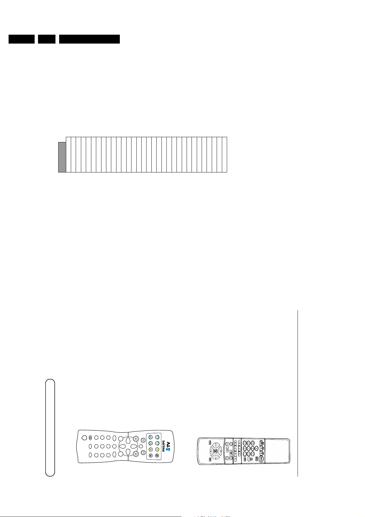
Installing the remote control
• Remove the cover at the back of the remot e
• Insert the correct type and size batteries into
You can secure your batteries by fastening
an appropriate screw into the hole.
the compartment m aking sure they are the
right way around.
•
Tips and Alerts
always contact a qualified technician.
recycled and reused by specialized
companies. Please find out about local
regulations on the disposal of your old TV
set.
Energy consumption contributes to air and
water pollution. We advise you to switch off
your TV overnight instead of leaving it in
stand-by mode.
L9 Quick DFU
• Never try repairing the set by yourself,
• Your T V contains material which can be
• TV c onsumes energy in the stand-by mode.
Accessing the Set-up Menu
Accessing the Set- up Menu, while the set is in
the Security High state, can only be done by a
T374AH Institutional Setup remote Menu
command.
While the set is in the Security Standard State
the Setup Menu may be accessed with a normal
guest cursor remote control by a sequence of
numbers (319753MUTE)
12NC: 3119 105 24841
4
9
3
6
5
8
7
12
4
TEXT
SMART
b
OK
0
`
MENU
2
MESSAGESLEEP
4
RC2882/01
Remote Controls used
For explanation in this manual, RC2882/01
is used. Remote control T374AH is an
accessory to be purchased separately . Refer to its
accompanying guide T374AH Remote Control Instruc-
tions for details of its operation.
TV
INFO
H
PAY TV RADIO
ALARM
A
ALARM OFF
T374AH
(RG4172BK)
(Optional)

Directions for use
Brightness
The brightness control contains 64 discrete
values from the minimum to maximum setting.
Colour
The color control contains 64 discrete values
STORE
To store the data of the menu, press right button.
from the minimum to maximum setting.
Contrast
The picture control contains 64 discrete values
from the minimum to maximum setting.
Sharpness
The sharpness control contains 64 discrete values
from the minimum to maximum setting.
Noise Reduction
Switch this on to reduce picture noise
Forced mono (for stereo TVs only)
This command is used to activate or to deactivate
the stereo feature, in stereo sets; toggle ON, OFF
using the right/left cursor.
Balance (for stereo TVs only)
It balances the sound output from TV’s speakers
Treble (for stereo TVs only)
It sets the treble frequencies of sound output
from TV’s speakers.
Bass (for stereo TVs only)
It sets the bass frequencies of sound output from
TV’s speakers.
AVL (Automatic Volume Leveller)
GB 7L9H.2E 3.
3
Protection
This menu item will be used to “Protect” or
“Lock” each program individually.
Label
This menu item will be used to add a label/name
for each program.
Store
This menu item is used to store the information
displayed in the Radio installation sub menu
Clock Installation
The Clock Installation menu is displayed when
the Clock Installation menu item is selected by
has a protection or not. With the cursor left/right
keys the protection can toggle between “YES”
and “NO”.
Label
This menu item will be used to add a label/name
for each program. Pressing the left/right buttons
you may enter or exit the label field; pressing the
up/down cursor you may insert alphanumeric
characters.
TXT Language
This menu enables the user to select the teletext
character set to be used for the selected channel.
With cursor left/right you can select a letter
corresponding to the different language clusters.
highlighting the Clock Installation menu item
with either Cursor Up or Cursor Down.
Time Setting
This menu item will be used to set the time for
the clock.
Display Standby
This menu item will be used to set the intensity
of the display of the clock when the TV is in
standby mode.
Display On
This menu item will be used to set the intensity
Video Blank
This item can change between “YES” and “NO”
to indicate if a picture mute is necessary.
Audio Mute
This item can change between “YES” and “NO”
to indicate if a sound mute is necessary.
Remarks
TV up/down, INFO up/down, PAY-TV up/down
and RADIO up/down are active in menu mode
and the TV reacts the same way as in TV mode.
Radio Installation Menu
of the display of the clock when the TV is in the
On mode.
Time Downloading
This menu item will be used to activate or
deactivate the time downloading function.
Teletext Program
This menu item will be used to select the channel
from which to retrieve the correct time from the
teletext. When this item is selected the TV set
tunes to the selected program.
Time Offset
This menu item will be used to set the offset
This menu appears only if an internal radio is
installed. The following subset of the TV
installation menu items is displayed and has the
same functionality: search, program, label,
protection, store, exit. The frequency range for
internal radio is 87.50 - 108.00 MHz FM. Beside
program “RAD XX” appears, where XX is the
selected program number; the type is RAD and is
not selectable.
Search
The Search function is activated by pressing the
“+” or Cursor Right button via the local
keyboard or remote control.
L9 Quick DFU
needed to adjust the time received from the
teletext channel to represent the current time in
the current location.
Program
The user can cursor down to the “Program”
menu item until it is highlighted and select a
program number via the Digits, Cursor Right, or
Cursor Left commands.
12NC: 3119 105 24841
2
Number of TV, Pay TV, Radio and Info
programs can be set and stored.
TV Installation Sub-Menu for the Set-up
Menu.When this menu is open, all the protections are
inactive.
To exit any menu press Menu button.
Input
The “Input” menu item selects the desired input
source that will be assigned to the program.
Possible values are Front End, AV1, and
AV2YC (internal interface, for system TVs
only).
System
Sets for East regions will have 2 states, WEST
EU (PAL/SECAM-BG) and EAST EU
(PAL/SECAM-DK).
Sets for West regions will have 3 states, WEST
EU (PAL/SECAM-BG), UK (PAL-I), FRANCE
(SECAM-L/L').
Manual Search
3 digits can be entered for a frequency in MHz or
radio tuner is present in the chassis), “RADIO”
is displayed, if the radio is internal there will be a
separate radio installation menu. If the program
number of a certain type is 0, the corresponding
type is not displayed.
right cursor for auto search; during frequency
entry the not yet entered digits are displayed as
dashes ‘-‘.
Program no.
The programme type can be selected with the
cursor left/right buttons. These buttons will
toggle between all available types: “TV”,
“INFO”, “PAY-TV”; if the radio is external (no
Store
fine-tuning.
Protection
The present program information, is stored after
pressing the cursor left/right button. Press Menu
to exit without storing.
Fine Tune
This bit indicates whether the selected program
Using the “control left/right” commands starts
L9 Quick DFU
12NC: 3119 105 24841

GB 8 L9H.2E3.
Directions for use
5
Guide
Welcome Message
When the “Welcome Message” menu item is
highlighted, the message “Press +” will appear in
The Power On Menu function is shown as
'POWER ON', and its valid states are
‘FORCED’: 'STANDARD'.
Program
This feature checks for program labels that have
been assigned to the programs via the LABELS
function, and if those programs are in the
the status section. When the user depresses “+”
or Cursor Right key, the following sub-menu
will be displayed: Message, Line 1, Line2,
Program Display
Program Display values can be: Number, Label,
program ring, will display in a “list” or “page”,
the program numbers with the associated labels.
All, None.
Keyboard Lock
In Commercial Mode, the Keyboard Lockout
menu function controls whether any Local
When the Reminder function is highlighted, the
status message displays the current state of the
Reminder
Keyboard commands, except for the Service
entry command can be generated.
The Keyboard Lockout menu function is shown
control.
This menu function is shown as 'REMINDER',
and its states are ‘ON’: 'OFF'.
as “KEYBOARD LOCKOUT” and its states are
‘ON’:’OFF’.
Security
The menu function “SECURITY” allows the
user to select one of two states “HIGH” or
“STANDARD”. The default is “STANDARD”.
Free protected programs
With this item all protected programs can be
freed. If “free protected programs” is set to
“yes”, all programs are accessible for the user, if
the item is “no” protected programs can be
selected but with picture and sound are muted.
While the set is in the Security High state the
setup menu can only be accessed by a T374AH
Institutional Setup remote menu command.
While the set is in the Security Standard state the
Setup Menu may be accessed with a normal
guest cursor remote control by a sequence of
numbers.
ESP
Energy Saving Programmability Mode (ESP)
controls the maximum continuous viewing time
allowed by the control system.
its valid values are 00 - 99 (in hours).
It is provided to allow the installed establishment
to limit the time the television remains activated
once a Guest has checked-out of their room.
The ESP Menu function is shown as ‘ESP’, and
System Interface
L9 Quick DFU
4
is used to enable or disable communication with
the DCM.
This item is only present in “system” sets and it
Audio/Video Mute
The Audio/Video Mute menu function
determines whether the video should be blanked
and the audio should be muted if the currently
tuned channel has no valid video information.
12NC: 3119 105 24841
The Automatic Volume Leveler feature is
shown as 'AVL' in the menu and its valid states
are ‘ON’: 'OFF'.
Volume Bar
To display volume bar when adjusting volume,
select ON; to hide the bar, select off.
Min Volume
It sets the limit for the minimum volume allowed
for the TV set; use right/left cursor to adjust.
Max Volume
It sets the limit for the maximum volume
allowed for the TV set; use right/left cursor to
adjust.
Switch on Volume
It sets the TV’s volume at switch on; use the
right/left cursor to adjust.
Volume Fixed
The feature is displayed as ‘VOLUME FIXED’
in the Setup menu and the valid toggle states are
‘ON’ and ‘OFF’.
Buzzer Volume
It sets the volume of the alarm buzzer; use
right/left cursor to adjust.
Switch On Program
This feature sets the current program that the
television will be tuned to when brought to
POWER ON condition.
Power On
The Power On menu function directs the control
system to activate the television receiver
whenever AC Power is applied to the television
and ignore any command that would deactivate
the television.
L9 Quick DFU
12NC: 3119 105 24841

Mechanical instructions
4. Mechanical instructions
GB 9L9H.2E 4.
4.1 Service positions
See figure 4-1 for the service position.
Disconnect the connecting cable feeding the right-hand and the
left-hand speaker, also disconnect the degaussing cable.
1
11
The mono-carrier is removed by pushing the two centre clips at
both chassis brackets outwards and pulling the panel forward.
A B
Figure 4-1
CL 96532047_015.eps
280599
5. Service Modes, DST, error messages, protections, fault finding
and repair tips
In this chapter the following paragraphs are included:
5.1 Test points
5.2 Service Modes
5.3 The menus and submenus
5.4 Error code buffer and error codes
5.5 The “blinking LED” procedure
5.6 Customer service mode ( CSM )
5.7 ComPair
5.8 Ordering compare
5.9 Trouble shooting tips
5.1 Test points
The main chassis is equipped with test points in the service
printing. These test points are referring to the functional blocks:
• A1-A2-A3, etc.: Test points for the AM Mono Demodulator
( A9 ), ITT panel ( D1) and Sound amplifier ( D2 )
• C1-C2-C3, etc.: Test points for the control circuit ( A7 ) and
the front control ( A8 )
• F1-F2-F3, etc.: Test points for the frame deflection circuit (
A3 )
• I1-I2-I3, etc.: Test points for the Tuner Video IF circuit ( A5 )
• L1-L2-L3, etc.: Test points for the Line deflection circuit (
A2 )
• P1-P2-P3, etc.: Test points for the power supply ( A1 )
• S1-S2-S3, etc.: Test points for the synchronisation circuit (
( A4 )
• V1-V2-V3, etc.: Test points for the video processing circuit
panel ( A6 ) and CRT panel ( B )
Measurements are performed under the following conditions:
• Video: colour bar signal
• audio: 3kHz left, 1kHz right
• Set in SDM mode
5.2 Service modes
The set has four services modes:
• Service Default Mode (SDM)
• Service Alignment Mode (SAM)
• Customer Service Mode (CSM)
• COMPAIR mode
5.2.1 Service Default Mode (SDM)
The purpose of the SDM is:

GB 10 L9H.2E5.
Service Modes, DST, error messages, protections, fault finding and repair
• provide a situation with predefined settings to get the same
measurements as in this manual
• start the blinking LED procedure
• Setting of options controls
• Inspect the error buffer
Entering the SDM:
• By transmitting the "DEFAULT" command with the RC7150
Dealer Service Tool (this works both while the set is in
normal operation mode or in the SAM)
• RC sequence 062596 followed by the key “MENU” (only
via set up remote, T374A)
The information displayed on the screen in the SDM mode is
given in fig. 5.1 (SDM menu).
Exit the SDM:
Switch the set to Standby or press EXIT on the DST (the error
buffer is also cleared).
Note: When the mains power is switched off while the set is in
SDM, the set will switch to SDM immediately when the mains
is switched on again. ( The error buffer will not be cleared ).
Pre-defined conditions
The SDM sets the following pre-defined conditions:
• Pal/Secam sets: tuning at 475.25 PAL (For France select
the L’-signal )
• Volume level is set to 25% (of the maximum volume level).
• Other picture and sound settings are set to 50%.
The following functions are “ignored” in SDM since they
interfere with diagnosing/repairing a set. “Ignoring” means that
the event that is triggered is not executed, the setting remains
unchanged.
• (Sleep)Timer
• Blue mute
• Auto switch off
• Hotel or Hospitality Mode
• Child lock or Parental lock
• Skipping, blanking of “Not favourite” present/channels
• Automatic storing of Personal Preset settings
• Automatic user menu time-out
All other controls operate normally.
5.2.2 Special functions in SDM
Access to SAM
By pressing the "MENU“ button on the remote control until SAM
is presented. (see fig. 5.1)
LLLL L9HBBC X.Y SDM
OP VALUE
OB1 OB2 OB3 OB4 OB5 OB6 OB7
ERR xx xx xx xx xx
MENU MENU
TV LOCK
MENU
INSTALLATION
BRIGHTNESS
COLOUR
CONTRAST
S
TUNER
WHITETONE
GEOMETRY
AKB
MENU
VSD
TV SETUP
L9HBBC X,Y
......
llllll
......
llllll
......
llllll
SAM
CL96532141_027.eps
S
31
31
31
171299
remains displayed in top of screen). Pressing the “MENU” key
again will return to the SDM mode.
Figure 5.1 Service Default Mode screens and structure
Explanation notes/references:
1. “LLLL” Operation hours timer (hexadecimal)
2. Software identification of the main micro controller
(L9HBBC X.Y)
• L9H is the chassis name for L9H
• BBC is 2 letter and 1 digit combination to indicate the
software type and the supported languages:
• X = (main version number)
• Y = (subversion number) BB = (range specification )
3. “SDM” To indicate that the TV set is in the service default
mode
4. “OP” Options Code which exists of 2 characters. It is
possible to change each option code
5. “VALUE” The value of the selected option ( ON/OFF or a
combination of 2 letters )
6. “XXX” Value of the options bytes ( OB1 .. OB7)
7. “ERR” The last five detected errors; The left most number
indicates the most recent error detected.
The cursor Up or cursor DOWN command can be used to
select the next/previous option; The cursor LEFT and cursor
RIGHT command can be used to change the option value.
Remark: When the option-code RC = OFF, the P+ and the Pkey have the same functions as the cursor UP/DOWN keys
while the VOL+ and the VOL- key have the same function as
the cursor LEFT/RIGHT keys. When the option RC = OFF it is
not possible to change the channel preset or to adjust the
volume when in SAM/SDM menu. Using a L9 remote control,
option-code RC = ON, the P+, P-, VOL- and VOL+ can be used
to change the preset and/or to adapt the volume, while the
menu-cursor keys are used to select the option and to change
its value.
For an extended overview of the option codes see Chapter 8 Options
5.2.3 Service Alignment Mode (SAM)
The purpose of the SAM is to do tuning adjustments, align the
white tone, adjust the picture geometry and do sound
adjustments.
For recognition of the SAM, “SAM” is displayed at the top of the
right side of the screen
Entering SAM:
• By pressing the "ALIGN" button command on the DST
RC7150 (Dealer Service Tool)
• When the set is in SDM by pressing the menu key or the
local keyboard keys “vol +” and “vol -“ simultantanously by
>4 seconds.
• Exit the SAM:
Switch the set to standby or press EXIT on the DST (the error
buffer is cleared).
Note: When the mains power is switched off while the set is in
SAM, the set will switch to SAM immediately when the mains is
switched on again. ( The error buffer will not be cleared ).
In the SAM the following information is displayed on the screen:
Figure 5-1
Access to normal user menu
Pressing the “MENU” button on the remote control until the
normal user menu (TV Set up; for TV lock, Installation,
Brightness, colour and contrast ) is presented while “S”

Service Modes, DST, error messages, protections, fault finding and repair
MENU
GB 11L9H.2E 5.
AAABBC X.Y
TUNER
WHITE TONE
GEOMETRY
AUDIO
AKB
VSD
L90 BBC X.Y
SOUND
SAM
SAM
MENU
MENU
MENU
L90 BBC X.Y
TUNER
IF-PLL
IF-PLL POS
AFA
AFB
L90 BBC X.Y
NORMAL RED
L90 BBC X.Y
SAM
64
192
1
1
SAM
40
SAM
A-FM
AT
STEREO
Access to normal user menu
Pressing the “MENU” button on the remote control will enter the
normal user menu ( TV lock, installation, brightness, colour and
contrast ) while “SAM” remains displayed in top of screen.
Pressing the “MENU” key again will return to the last SAM
status.
Access to SDM
Pressing the “DEFAULT” button on the DST
SAM menu control
Menu items (AKB, VSD, Tuner, White tone, Geometry and
Audio) can be selected with the cursor Up or cursor DOWN
key. Entry into the selected items (sub menus) is done by the
cursor LEFT or cursor RIGHT key. The selected item will be
highlighted.
With the cursor LEFT/RIGHT keys, it is possible to increase/
decease the value of the selected item.
232
4
15
Figure 5-2 Service Alignment Mode screens and structure
MENU
VAM
55
CL96532141_028.eps
071299

GB 12 L9H.2E5.
Service Modes, DST, error messages, protections, fault finding and repair
5.3 The menus and submenus
5.3.1 Tuner sub menu
The tuner sub menu contains the following items:
• IF_PLL : PLL Alignment for all PAL/SECAM
systems, excluding SECAM-LL’
• IF-PLL Pos
• IF PLL ofset
• AFW : AFC Window
• AGC : AGC take-over point
• YD : Default value = 12 ; Do not align
• CL : Default value = 4 ; Do not align
• AFA
• AFB
The items AFA and AFB can not be selected, they are for
monitoring purposes only.
The commands cursor UP and cursor DOWN are used to
select the next/previous item.
The commands cursor LEFT and cursor RIGHT are used to
increase/decrease the value of the selected item. The changed
values will be send directly to the related hardware.
The item values are stored in NVM if this sub menu is left.
5.3.2 White tone sub menu
The commands MENU UP and MENU DOWN are used to
select the next/previous item.
The commands MENU LEFT and MENU RIGHT are used to
increase/decrease the value of the selected item. The changed
values will be send directly to the related hardware.
The item values are stored in NVM if this sub menu is left.
The white tone sub menu contains the following items:
• NORMAL RED
• NORMAL GREEN
• NORMAL BLUE
• DELTA COOL RED
• DELTA COOL GREEN
• DELTA COOL BLUE
• DELTA WARM RED
• DELTA WARM GREEN
• DELTA WARM BLUE
OSD is kept to a minimum in this menu, in order to make white
tone alignment possible.
The Contrast Plus feature (black stretch) is set to OFF when
the white tone submenu is entered.
5.3.3 Audio sub menu
5.3.4 Geometry sub menu
The geometry sub menu contains the following items:
• SBL : Service blanking
• VSL : Vertical slope
• VAM : Vertical amplitude
• VSH : Vertical shift
• HSH : Horizontal shift
• EW: E-W amplitude (only if option EW=on)
• PW: E-W parabola/width (only if option EW=on)
• TC: E-W trapezium (only if option EW=on)
• VSC : Vertical scroll (only if option EW=on and 88=on)
• VX: Vertical zoom (only if option EW=on)
• CP: E-W corner parabola (only if option EW=on)
• SC: S correction
• H60 Delta HSH for 60Hz.
• V60 : Delta VAM for 60Hz.
• W43: Delta EW for 4:3 (only if option EW=on)
• S43: Delta VSL for 4:3
• A43: Delta VAM for 4:3 (only if option EW=on)
• C43: Delta SC for 4:3 (only if option EW=on)
• X43: Delta VX for 4:3 (only if option EW=on)
5.4 Error code buffer and error codes
5.4.1 Error code buffer
The error code buffer contains all errors detected since the last
time the buffer was erased. The buffer is written from left to
right.
• when an error occurs that is not yet in the error code buffer,
the error is written at the left side and all other errors shift
one position to the right
• the error code buffer will be cleared in the following cases:
1. exiting SDM or SAM with the “Standby" command on
the remote control
2. transmitting the commands “EXIT” with the DST
(RC7150)
3. transmitting the commands “DIAGNOSE-9-9-OK” with
the DST.
• The error buffer is not reset when the set is switched off by
the mains switch.
Examples:
• ERROR: 0 0 0 0 0 : No errors detected
• ERROR: 6 0 0 0 0 : Error code 6 is the last and only
detected error
• ERROR: 5 6 0 0 0 : Error code 6 was first detected and
error code 5 is the last detected (newest) error
The audio sub menu (for stereo sets only) contains the
following items:
• ST-NT : Stereo noise treshold (only if option
SB=50)
• SAP-NT : SAP noise treshold (only if option
SB=50)
• LA : Input level adjust (only if option
SB=50/52/55)
• WIDEB : Stereo adjust for wide band expander
(only if option SB=50/52/55)
• SPECT : Stereo adjust for special expander
(only if option SB=50/52/55)
• AT : Attack time at AVL (only if option
SB=52/55)
• STEREO : Stereo adjust MSP34xx (only if option
SB=IT/NB/NDIT)
The sound adjustments sub menu is not available in Mono
sets.
The presence of an item in the menu strongly depends on the
selected sound board (option SB).
5.4.2 Error codes
In case of non-intermittent faults, clear the error buffer before
starting the repair to prevent that “old” error codes are present.
If possible check the entire content of the error buffers. In some
situations an error code is only the RESULT of another error
code (and not the actual cause).
Note: a fault in the protection detection circuitry can also lead
to a protection.
a. Error 0 = No error
b. Error 1 = X-ray ( Only for USA sets )
c. Error 2 = High beam current protection
– High beam protection active; set is switched to
protection; error code 2 is placed in the error buffer; the
LED will blink 2 times ( repeatedly ).
– As the name implies, the cause of this protection is a
too high beam current (bright screen with flyback
lines). Check whether the +160V supply to the CRT
panel is present. If the voltage is present, the most
likely cause is the CRT panel or the picture tube.
Disconnect the CRT panel to determine the cause. If

Service Modes, DST, error messages, protections, fault finding and repair
1 HHHH L9HAP-X.Y CSM
2 CODES xx xx xx xx xx
3 OP xxx xxx xxx xxx xxx xxx xxx
4 SYS: AUTO AUTO
6
7 MODE COMMERCIAL
8 SMARTPORT OFF
9 CHANNEL TV1
CL96532141_029.eps
071299
GB 13L9H.2E 5.
the +160V voltage is not present, check R3416 and
D6409 ( Horizontal Deflection - A2 )
– EW protection:
– If this protection is active, the cause could be one of the
following items;
• LOT 5445
• S-correction capacitor 2407
• flyback capacitor 2434
• line output stage
• short circuit of flyback diode 6434
• Line uotput transistor 7402 or driver-transistor
7400
d. Error 3 = Vertical Guard
e. Error 4 = Sound processor ( IC7803 ) IIC error (
MSP3415D )
Sound processor does not respond to the micro controller
a. Error 5 = Bimos ( IC7250 ) start-up error ( POR bit )
b. Bimos start-up register is corrupted or the IIC line to the
Bimos is always low or no supply at pin 12 of the Bimos).
This error is usually detected during start-up and hence will
prevent the set from starting up.
c. Error 6 = Bimos (TDA884x ) IIC error
Note that this error may also be reported as a result of error
codes 4 (in that case the Bimos might not be the actual
problem)
a. Error 7 = General IIC error. This will occur in the following
cases:
• SCL or SDA is shorted to ground
• SCL is shorted to SDA
• SDA or SCL connection at the micro controller is open
circuit.
b. Error 8 = Microprocessor ( IC7600 ) internal RAM error ( A7
)
The micro controller internal RAM test indicated an error of the
micro controller internal memory (tested during start-up);
a. Error 9 = EEPROM Configuration error ( Checksum error );
EEPROM is corrupted.
b. Error 10 = IIC error EEPROM . NV memory (EEPROM)
does not respond to the micro controller
c. Error 11 = IIC error PLL tuner. Tuner is corrupted or the IIC
line to the Tuner is low or no supply voltage present at pin
9, pin 6 or pin 7 of the tuner.
5.6 Customer Service Mode (CSM)
The set is equipped with the “Customer Service Mode” (CSM).
CSM is a special service mode to identify the status of the set.
It can be activated and deactivated with the set-up remote
transmitter (RG4172BK). The CSM is a 'read only' mode,
therefore modifications in this mode are not possible.
5.6.1 Entering the Customer Service Mode (in “Commercial
mode)
The Customer Service Mode can be switched on by pressing
RECALL on the set-up remote control RG4172BK.
When the CSM is activated:
• picture and sound settings are set to nominal levels
•“Service unfriendly modes” are ignored
• In “Consumer mode”: RC “Mute” = local keyboard buton >4
seconds simultaneously
5.6.2 Exit the Customer Service Mode
The Customer Service Mode will switch off after:
• pressing one of the keys RECALL or MENU on the set-up
remote control RG4172BK
• switching off the TV set with the mains switch.
All settings that were changed at activation of CSM are set
back to the initial values
5.6.3 The Customer Service Mode information screen
The following information is displayed on screen:
5.5 The “blinking LED” procedure
The contents of the error buffer can also be made visible
through the “blinking LED” procedure. This is especially useful
when there is no picture. There are two methods:
• When the SDM is entered, the LED will blink the number of
times, equal to the value of the last (newest) error code
(repeatedly).
• With the DST all error codes in the error buffer can be
made visible. Transmit the command: “DIAGNOSE x OK”
where x is the position in the error buffer to be made visible
x ranges from 1, (the last (actual) error) to 5 (the first error).
The LED will operate in the same way as in point 1, but now
for the error code on position x.
Example:
Error code position1 2 3 4 5
Error buffer:8 9 5 0 0
• after entering SDM: blink (8x) - pause - blink (8x) - etc.
• after transmitting “DIAGNOSE- 2- OK” with the DST blink
(9x) - pause - blink (9x) - etc.
• after transmitting “DIAGNOSE- 3- OK” with the DST
blink(5x) - pause - blink(5x) - etc.
• after transmitting “DIAGNOSE- 4- OK” with the DST
nothing happens
Figure 5-3
Fig 5-3 cl96532141-029Screen lay-out CSM
A line number is placed for every line in order to make CSM
language independent.
– Line 1: Operating hours/ Software version L9HBBC X.Y)/
Text “CSM”; to indicate that the set is in the Customer
Service Mode
– Line 2: Error buffer contents (see paragraph 5.4.2)
– Line 3: Option code information (see chapter 8)
– Line 4: Configuration information. SYS: xxxx xxxx
indicates the colour and sound system preset
– Line 5: “ Not tuned when no signal is received ”.
– Line 6: not used
– Line 7: Mode. Indicates whether the set is in commercial or
consumer mode
– Line 8: SmartPort. Indicates whether the Smart Port is
selected or nor.
– Line 9: Channel. Indicates the selected channel.

GB 14 L9H.2E5.
Service Modes, DST, error messages, protections, fault finding and repair
5.7 ComPair
5.7.1 Introduction
ComPair (Computer Aided Repair) is a service tool for Philips
Consumer Electronics products. ComPair is a further
development on the DST service remote control allowing faster
and more accurate diagnostics. ComPair has three big
advantages:
• ComPair helps you to quickly get an understanding how to
repair the sets in short time by guiding you step by step
through the repair procedures.
• ComPair allows very detailed diagnostics (on I
is therefore capable of accurately indicating problem areas.
You do not have to know anything about I
yourself; ComPair takes care of this.
• ComPair speeds up the repair time since it can
automatically communicate with the sets (when the micro
processor is working) and all repair information is directly
available. When ComPair is installed together with the
SearchMan electronic manual, schematics and PCBs are
only a mouse-click away.
ComPair consists of a Windows based fault finding program
and an interface box between PC and the (defective) product.
The ComPair interface box is connected to the PC via a serial
or RS232 cable. In case of the L9H chassis, the ComPair
interface box and the L9H communicate via an IIC cable (bidirectional) and via infra red communication (uni-directional;
from ComPair interface box to L9H.
The ComPair fault finding program is able to determine the
problem of the defective television. ComPair can gather
diagnostic information in 2 ways:
1. Communication to the television (automatic)
2. Asking questions to you (manually)
ComPair combines this information with the repair information
in its database to find out how to repair the set.
Automatic information gathering
Reading out the error buffer, ComPair can automatically read
out the contents of the entire error buffer.
Diagnosis on I
television. ComPair can send and receive I
micro controller of the television. In this way it is possible for
ComPair to communicate (read and write) to devices on the I
busses of the
2
C level. ComPair can access the I2C bus of the
2
C commands to the
2
C level) and
2
C commands
By a combination of automatic diagnostics and an interactive
question/answer procedure, ComPair will enable you to find
most problems in a fast and effective way.
Additional features
Beside fault finding, ComPair provides some additional
features like:
• Uploading/downloading of presets
• Managing of preset lists
• Emulation of the Dealer Service Tool
Connecting the ComPair interface
The ComPair Browser software should be installed and set-up
before connecting ComPair to the set. (See the ComPair
Browser Quick Reference Card for installation instructions.)
Connect the RS232 interface cable to a free serial
1.
(COMM) port on the PC and the ComPair interface PC
connector (connector marked with "PC").
Place the ComPair interface box straight in front of the
2.
television with the infrared window (marked "IR")
directed to the television LED. The distance between
ComPair interface and television should be between
0.3 and 0.6 meter. (Note: make sure that (also) in the
service position, the ComPair interface infra red
window is pointed to the standby LED of the television
set (no objects should block the infra red beam)
Connect the mains adapter to the connector marked
3.
"POWER 9V DC" on the ComPair interface
Switch the ComPair interface OFF
4.
Switch the television set OFF with the mains switch
5.
Remove the rear cover of the television set
6.
Connect the interface cable (4822 727 21641) to the
7.
connector on the rear side of the ComPair interface
that is marked “I
Connect the other end of the interface cable to the
2
C
8.
ComPair connector on the mono-carrier (see figure 5-
2
C” (See Figure 5.5)
6)
Manual information gathering
Automatic diagnosis is only possible if the micro controller of
the television is working correctly and only to a certain extend.
When this is not the case, ComPair will guide you through the
fault finding tree by asking you questions and showing you
examples. You can answer by clicking on a link (e.g. text or an
waveform pictures) that will bring you to the next step in the
faultfinding process.
A question could be: Do you see snow? (Click on the correct
answer)
YES / NO
An example can be: Measure test point I7 and click on the
correct oscillogram you see on the oscilloscope
I7 B7502
1V / div DC
10µs / div
Figure 5-4
Plug the mains adapter in the mains outlet and switch
9.
ON the interface. The green and red LED light up
together. The red LED extinguishes after approx. 1
second (the green LED remains lit).
Start-up ComPair and select “File” menu, “Open...:;
10.
select “L9.2 Fault finding” and click “OK”
Click on the icon (fig. 5.6) to switch ON the
11.
communication mode (the red LED on the ComPair
interface will light up)
Switch on the television set with the mains switch
12.
When the set is in standby. Click on “Start-up in
13.
ComPair mode from standby” in the ComPair L9H fault
finding tree, otherwise continue.

Service Modes, DST, error messages, protections, fault finding and repair
5.9 TROUBLE SHOOTING TIPS
In this paragraph some trouble shooting tips for the deflection
and power supply circuitry are described. For detailed
diagnostics, check the fault finding tree or use ComPair.
GB 15L9H.2E 5.
Figure 5-5
PC VCR I2CPower
Figure 5-6
The set has now started up in ComPair mode. Follow the
instruction in the L9.H fault finding tree to diagnose the set.
Note that the OSD works but that the actual user control is
disabled
5.8 Ordering ComPair
ComPair order codes:
• Starter kit ComPair + SearchMan software + ComPair
interface (excluding transformer): 4822 727 21629
• ComPair interface (excluding transformer): 4822 727
21631
• ComPair transformer (continental) Europe: 4822 727
21632
• ComPair transformer United Kingdom: 4822 727 21633
• Starter kit ComPair software: 4822 727 21634
• Starter kit SearchMan software: 4822 727 21635
• Starter kit ComPair + SearchMan software: 4822 727
21636
• SearchMan CD (update): 4822 727 21638
• ComPair interface cable (for L9): 4822 727 21641
MAIN PANEL COMPONENT VIEW
HOT GROUND
BORDER
13
0267
COMPAIR
9V DC
86532027_003.EPS
050898
0231
5.9.1 THE DEFLECTION CIRCUIT:
1. Measure the +VBATT ( 95V) is present across 2551 ( A2 Line deflection ). If the voltage is not present, disconnect
coil 5551. (Horizontal deflection stage is disconnected). If
the voltage is present then the problem might be caused by
the deflection circuit. Possibilities:
• Transistor 7402 is faulty
• The driver circuit around transistor 7400 is faulty
• No horizontal drive signal coming from the BIMOS
7250-D pin 40 ( A4 - Synchronisation )
• Timer-IC 7607 or transistor 7608 is defect ( A7 -
Control )
2. Note: If the Collector of 7402 is shorted to the Emitter, hickup noise can be heard from the power supply. In this case
the E/W protection is disabled. is correctly working ( a
parabolic picture )
3. Also take note of protection circuits in the line output stage.
If any of these circuits are activated, the set will shut down.
Depending on the protection, the led will blink according to
the fault defined. In order to determine which protection
circuit is active, isolation of each separate circuit is
necessary. These protection circuits are:
• High beam current protection ( LED blinks repetitively
2 times ) - CRT panel ( B )
• Vertical protection ( LED blinks repetitively 3 times ) -
Vertical deflection ( A3 )
5.9.2 THE POWER SUPPLY
To trouble shoot the L9 SMPS, first check the Vaux voltage on
C2561. If this voltage is not present, check fuse F1572 and
D6560. If F1572 or D6560 is not open circuit, the problem might
be caused on the primary side of the switching supply. Check
the output of the bridge rectifier on C2508 for approximately
300V DC at an input voltage of 230Vac. If this voltage is
missing, check the bridge diodes 6502 .. 6505 and the fuse
1500. If fuse F1500 is found open, check MOSFET 7518 to
make sure that there is no short circuit present and check
R3518. If the 300V DC is present on C2508, check for a startup voltage of approx. 13V on pin 1 of IC7520. If no start-up
voltage is present, check if R3510 is open or diode 6510 is a
short-circuit. It is necessary to have a feedback signal from the
hot primary side of switch mode transformer T5545 at pin 1 and
pin 2 for the power supply to oscillate. If the start-up voltage of
13V is present on pin 1 of IC7520 and the supply is not
oscillating, check R3529 and D6540.
Check for a drive signal at the gate of MOSFET 7518, square
wave signal - P1. Check pin 3 of IC7520 and R3525.
To determined whether OVP is active, check the presence of
Vaux at C2561.
TUNER
1000
CL 96532028_013a.eps
220499
Figure 5-7
GB 16 L9H.2E5.
5.10 Faultfinding trees
Service Modes, DST, error messages, protections, fault finding and repair
100100
code
R3510,R3529
Check/Replace
1 11 1
Check/Replace
(A1);SW0231,F1500,D6502,D6503,D6504,D6505
Note: If F1500 is defective, then also check R3504
1 11 1
Yes
present?
(A1); <P1>
No
Any secondary
voltage present ?
No No
(A1);D6540,C2540,D6510,
Voltage
present?
(A1);<P3>
No No
startpuls
present?
(A1); <P2>
Yes
3V3,
Check
(A7); <C1>,<C4(reset)>
1 17 3
Yes
IC7600
Check/Replace
TS7602,TS7605
1 11 A
X1600
(A8);LED6690
R3525
(A1);IC7520
Check/Replace
Yes
(F), <P10>
System Sets
Check / Replace
Check/Replace
(A1);TS7518,L5552
1 11 1
No
present ?
TR5545 pin9
(A1); voltage on
(J); F1700
<P13>; T1, CR1
D1106, F1, L1, L2
<P11>; IC1, T1, IC2
<P12>; T1, CR2, IC4
Note 1:
Yes
Check/Replace
1 11 A
F1920
(H1); IC7920
NON System Sets
A
1 11 A
1 11
IRIS SYMPTOM CODE
(A1);L5540,D6540,C2540
Extended symptom
code
Main symptom
Note 2:
code
Condition
CL 06532004_006.eps
(A1) means Drawing A1
<P1> means Test point P1
hicking ?
Is the Power supply
Remark :
intensity and in
lights in full intensity
Red LED lights in half
standby-mode the LED
In normal operation the
continuously
Does the red LED
light in full intensity
No No
START
Does the red LED
full intensity, one time
Put the Mainsswitch : on.
PAL B/G (for France SECAM l).
Connect a pattern generator to the arial input.
Set Patt.gen. to 475,25 MHz, colourbar, stereosound,
picture and sound will appear.
after a few seconds more in half intensity while the
blinking for one second in full intensity, one time then
In normal conditions the set will start with the Red LED
blink for one second in
Yes
1 11 D
?
?
Yes
disappear.
is too high.
The load of the power supply
Isolate each branch of the load
Yes
A
No
?
appear properly
Do picture and sound
the overload.
one by one, until the hicking
for the branch, which causes
Continue with the fault finding
Ensure communication
Yes
Vaux
+VBATT
MainSupply
(A1);AudioSupply
The branches are:
(A8);IC7680
with the RC,
Check/Replace
Put the set into the
Service Default Mode
either via the DST or by
An error code is
LED via the SDM.
or via the service pins
the RC in the following
order :062596<MENU>,
pressing the buttons on
indicated by the blinking
error n.
detailled information
See also chapter 5.5 for
n-times blinking means
Set is OK
B
Yes
indication ?
Is there an error
No
for details
list via CSM see
chapter 5.5 of this
manual
Check / correct Options
Figure 5-8

Service Modes, DST, error messages, protections, fault finding and repair
GB 17L9H.2E 5.
100199
NO Radio
Pictures are not
Deflection not OK
symetrical and unstable
Menu OK
NO Sound
NO Picture
1 12 0
R3927
(H1) IC1901
R3925, R3926
IC7904, D6925
IC7901, IC7903
Check / Replace
C
D6007,
(A5);Antenna,
Check / Replace
(A6);X1205..X1208
IC7250
Check / Replace
1 11 A
No
Sound and Picture
from external source
OK ?
Yes
1 12 0
Tuner1000
Check / Replace
Nicam/2CS
MSP3415D
Ok ?
(D1);<A20>
No
(D1);
Conn0239
(A5);TS7266
Check / Replace
TS7801, TS7802
Yes
Check / Replace
Ok ?
;<A22>
(P1);<A21>
No
IC7803
+5VB,x1801,
(D1);+8V,+5VA,
Yes
(D2);<A25>
Check / Replace
(D2);Audio Supply
<28> Ok ?
<A26><27>
No
IC7954
IC7953 or
10V / 14V
Yes
Check / Replace
(D2);Conn,0246,
Speakers
Conn,0247
CL 06532004_008.eps
(I) CONN, J3
CONN, U3, R9, R10
(l,r,l+r)
Menu OK
NO Sound
Picture OK
No Menu
No picture
Black screen
(Colour missing)
1 13 0
Sound OK
OK ?
(A5); <L1>
No
(A5); Tuner 1000
Check / Replace
L5341
L5342,CRT,
(B);Conn.0244,
Check / Replace
(A2);L5480,Conn.0220
No
?
OK
(B);
Heater / Filaments
No
Yes
Yes
OK ?
(A5); <L2>
No
(A5); IC7250
Check / Replace
Adjust VG2
(A2);TR5445,
Check / Replace
1 13 0
No
(B);VG2
Yes
Mono versions
CRT
(B);R3341,C2341
?
OK
1 13 0
Yes
Yes
Ok ?
(A5);<I9>
No
FIL1002
(A5); TS7268,
Check / Replace
TS7000,FIL1001,
(A3);IC7401,
Check/Replace
D6460.C2464,D6461
No
?
OK
(A3);<F3>,<F4>
Ok ?
(A5);<I4>
No
(A5); IC7250
Check / Replace
1 13 0
Yes
Yes
(A10);<A3>
Check / Replace
Check/Replace
(A6);IC7250-B/C
No
OK
<V6,V7,V8>
(A6);<V1..V4>
Ok ?
No
(A10); TS7951,
Yes
Yes
1 13 0
Ok ?
(A10);
<A4>..<A5>
No
or
IC7954
(A10);IC7953
Check / Replace
CRT Socket,
TS7333,160V
Check/Replace
(B);Conn0245,IC7311,
No
OK
(B);<V11..V16>
Yes
Yes
1 13 0
Loudspeaker
Check / Replace
(A10);Conn.0215,
(B);CRT
Check/Replace
conn. 1940,
RADIO SET:
IC7901, IC7904
(H1) conn. 0264,
A
with the RC,
Ensure communication
(A8);IC7680
Check/Replace
Put the set into the
Service Default Mode
either via the DST or by
An error code is
or via the service pins
the RC in the following
order :062596<MENU>,
pressing the buttons on
indicated by the blinking
error n.
LED via the SDM.
detailled information
See also chapter 5.5 for
n-times blinking means
?
Yes
indication
Is there an error
If the mainsupply or
not be reliable. So in
EHT is missing, then
the error message may
Figure 5-9
the
schematics ;
(A1), (A2) and
the first place see
components of the
this state check/replace
(A4);IC7250-D <S2>
mainsupply and EHT in
B

GB 18 L9H.2E5.
ERR 10
No
and/or
ERR 4
Yes
11
EEPROM error
1 17 X
Yes
Check
+5 V Protection
Service Modes, DST, error messages, protections, fault finding and repair
100100
C
2
- When I
signals or the
+5D are missing
on IC7601 the set
ERROR 11
(A2); +VLotAux+5V
Message :
store any data.
ERR 10 0 0 0 0
can function, but
will not be able to
C Tuner error
2
I
1 12 0
(A7); +5VD
IC7601 pin 5,6
Check/Replace
too
- It is possible
will be reported
that during +5V
protection Error 4
Message :
CheckReplace
ERR 11 0 0 0 0
(A5);Tuner1000
ERROR 9
New micro controller or
is defective
CL 06532004_007.eps
persists, then IC7601
were loaded. Re-align
the set. If the problem
EEProm.Default values
No
3, 12
ERR 1,
NoNo
or 6
ERR 5
Yes
ERROR 1 ERROR 3
BIMOS error.
1 11 A
ERROR 4
17 X
1
Protection.
Vertical / Frame
1 11 D
- Before the proctection
Protection.
- When the X-Ray
(USA version only)
X-Ray/Over-voltage
1 17 8
C
2
Message :
of the BIMOS
ERR 4 6 0 0 0
because there is no
The error is detected,
communications on I
Message :
ERR 4 0 0 0 0
In this situation the set
Fault in audio section
turns on without sound.
visible for 3 sec.
- During Vertical /
is really actived, a
horizontal line will be
set will hicc-up until the
protection is started, the
C
2
(A4,A5) ; the
CheckReplace
+8VBIMOS and the I
turn on and so the
Frame protection the
EHT will not be able to
protection mode.
voltage at pin 50 of
3.9 V the set is put in
IC7250 becomes >3.9
Volts. At the voltage of
lines pin7,8 of IC7250
Check/Replace
7803 pin9,10.
(A10); +VlotAux+5V,
Message :
available. As such
and Sound IC is not
VlotAux5V to the Tuner
to turn on and so the
the EHT will not be able
- During x-ray protection
ERR 11 4 3 0 0
11 will be reported too.
ERROR 4 and ERROR
available. As such
and Sound IC is not
VlotAux5V to the Tuner
11 will be reported too.
ERROR 4 and ERROR
Conn0222
(A3);IC7460
C2464,D6460
Check / replace
C error.
2
Yes
to each other.
line of all units for
General I
Check SCL and SDA
1 17 8
No
Yes
ERR 2 ERR 7
No
B
ERR 8
Yes
Protection.
High beamcurrent ,
E/W and Horizontal
1 11 D
error
1 17 8
uP Internal RAM
- When the High
Check / replace
only be read by
The Error code can
shortcircuit to ground or
putting the TV set into
protection.
beamcurrent protection
is started, fly-back lines
will be visible for 15 sec.
before the set is really in
(A7);IC7600
Check / replace
the SDM mode. The
- When E/W or
Horizontal protection is
(A6);IC7250-C pin7,8
(A7);IC7600 pin49,50
(A5);Tuner1000 pin4,5
LED will blink 7 times.
activated.
- During E/W or
protection is really
up for 4sec. before the
started, the set will hicc-
(A7);IC7601 pin5,6
(A10); IC7833 pin9,10
to turn on and so the
Horizontal protection
the EHT will not be able
As far as
applicable
causes the error.
Replace the item, which
available. As such
and Sound IC is not
VlotAux5V to the Tuner
(H1); IC7904 pin 14, 15
(G1); IC7951 pin 23, 24
Message :
ERR 11 4 2 0 0
11 will be reported too.
ERROR 4 and ERROR
(I), D1, D2, U1
(J), Smart Card
or
+160V supply
(CRT);R3340,
Check/Replace
(A2);Conn.0221
E/W,Horizontal Prot.
Figure 5-10

Service Modes, DST, error messages, protections, fault finding and repair
C
Horizontal section
Picture unstable
horizontally.
Picture width too
small.
No sync.
E/W not ok
(A4) ; <S2>,
OK
?
1 53 0
Check / Replace
No
(A4);IC7250
Vertical section
Vertical picture is
too small or unstable
(A4);<S3>,<S4>
OK
?
Yes
No
GB 19L9H.2E 5.
1 53 0
Check / Replace
(A4); IC7250
1 17 8
Yes
1 33 A
Check / Replace
(A2) TS7400,TS7402,
LOT 5445,C2407,
(A7) IC7607,
TS7608
Figure 5-11
(A3);<F3>,<F4>,
<F5> OK
?
Yes
1 17 8
Check / Replace
(A3);Vertical defl. coil
L0222
Check / Replace
No
IC7460,R3463,
R3465,R3466,
D6460,C2464
CL 96532028_011.eps
290399

GB 20 L9H.2E5.
Personal notes:
Service Modes, DST, error messages, protections, fault finding and repair

Alignments
CL 96532141_007.eps
241199
1000
TUNER
LOT
HOT GROUND
BORDER
7600
7518
MAIN PANEL COMPONENT VIEW
VBATT ADJ
95V
3540
AUDIO PANEL
uC
FOCUS
VG2
8. Alignments
GB 47L9H.2E 8.
General: the Service Default Mode (SDM) and Service
Alignment Mode (SAM) are described in chapter 5.
8.1 Alignment conditions
All electrical adjustments should be performed under the
following conditions:
• Supply voltage : 220V - 240V ( 10% )
• Warm-up time: 10 minutes
• The voltages and oscillograms are measured in relation to
the tuner earth.
• Test probe: Ri > 10MΩ Ci < 2,5 pF.
• Pattern generator (e.g. PM5518) set to 475.25 MHz
and.default transmission system for your country with RF
signal amplitude of 10mV connected to the aerial input of
the TV.
• SDM switched on.
8.1.1 Entering Service Default Mode (SDM)
• By transmitting the "DEFAULT" command with the RC7150
Dealer Service Tool
• Standard RC sequence 062596 followed by the key
“MENU”
8.1.2 Entering Service Alignment Mode (SAM)
• By pressing the "ALIGN" button command on the RC7150
Dealer Service Tool
• when the set is in SDM by pressing the MENU key until
SAM is presented
values (do not switch the set to STANDBY first, this will
change the default settings of the set).
• Switch ON the set. Switch the set to STANDBY to leave
SDM.
8.2.3 Focusing
• Set the pattern generator to display a Circle with Small
Squares pattern.
• Adjusted with focusing potentiometer, positioned at LOT
5445 (see Fig.8.1), for maximum sharpness of the picture.
8.2 Electrical Alignments
8.2.1 Adjustment of the Power Supply
• Set the pattern generator to display a Circle with Small
Squares pattern.
• Connect a DC voltmeter to capacitor 2409.
• Adjust potentiometer R3540 (see Fig. 8.1) till the voltmeter
indicates 95V.
8.2.2 VG2
• Set the pattern generator to display a black picture.
• Enter SDM.
• Select TV SETUP by pressing the MENU key on the RC
once.
• Press the MENU DOWN key on the RC until the
BRIGHTNESS sub-menu is selected and change the value
to 50 with the MENU LEFT/RIGHT key. Select the
CONTRAST sub-menu and change the value to 0.
• Select SAM by pressing the MENU key on the RC once.
• Press the MENU DOWN key on the RC until sub-menu
VSD (Vertical Scan Disabled) is selected and change the
value from 0 to 1 by pressing the MENU LEFT key.
CAUTION!! Depending on the position of the VG2 potentiometer, a bright coloured line will appear on the middle of
the screen or the screen will turn completely black.
• Adjust with VG2 potentiometer, positioned at LOT 5445
(see Fig.8.1), until the coloured line at the middle of the
screen is just not visible.
• The alignment of the VG2 has been completed now. Switch
OFF the set using the mains switch. The values adapted at
the BRIGHTNESS- and the CONTRAST sub-menu during
the alignment, will change back again to their default
Figure 8-1
8.3 Software adjustments
8.3.1 Geometry adjustments
• Set the pattern generator to display a Circle with Small
Squares pattern.
• Enter SAM.
• Select GEOMETRY menu.
• Using the MENU UP/DOWN keys on the RC the respective
items in the GEOMETRY menu can be selected. Use the
left/right buttons to adjust the selected items to correct the
picture geometry as stated below.
Vertical Amplitude and Position
• Select VSL (Vertical Slope) and shift the picture to the top.
The text VSL and its value should be at the upper half of
the screen.
• Select SBL (Service Blanking) and set it to 1. The lower half
of the picture will be blanked.
• Press the MENU UP key once to select VSL and align it to
start the blanking exactly at the horizontal white line at the
centre of the test circle. VSL has the correct value now and
should not be changed anymore.
• Press the MENU DOWN key once to select SBL and set it
to 0. The full picture reappears.

GB 48 L9H.2E8.
Alignments
• Select VAM (Vertical Amplitude) and align the picture
height such that the top horizontal line just disappears. This
corresponds with an over scan of approx. 6%.
• Select VSH (Vertical Shift) and align for vertical centring of
the picture on the screen.
• Repeat the last two steps if necessary.
• Select VSC (Vertical S-correction) to align the top/bottom
squares till they have the same size as the squares in the
middle of the screen.
Horizontal Amplitude and Phase
• Select HSH (Horizontal Shift) and adjust it for a correct
horizontal centring of the picture
For sets with East/West correction follow the instructions
below:
• Select EWW (East-West Width) and align the picture with
substantial over scan.
• Select EWT (East-West Trapezium) and align for a
rectangle if necessary
• Select EWP (East-West Parabola) and align for straight
vertical lines.
• Select EWC (East-West Corner) and align the corners.
• Repeat if necessary.
• Set H60 to 10 and V60 to 10.
• To store the alignments in the NVM, press the STANDBYkey on the RC.
8.3.2 AGC
• Set the pattern generator to display colour bar pattern.
• Connect a DC voltmeter at pin 1 of the tuner 1000.
• Enter SAM.
• Enter TUNER menu.
• Select AFW and align it for the lowest value.
• Select AGC and adjust it until the voltage at pin 1 of the
tuner is 1.0V +/- 0.1V.
• To store the alignments in the NVM, press the STANDBYkey on the RC.
• Enter WHITE TONE menu and select item NORMAL,
DELTAWARM, or DELTACOOL depending on the item
which has to be aligned. The items R, G and B can be
aligned according personal preference.
The default values for the colour temperature are displayed in
the table below:
NORMAL 11500K R = 40 G = 40 B = 40
DELTACOOL 13500K R = -2 G = 0 B = 6
DELTAWARM 8500K R = 2 G = 0 B = -7
• To store the alignments in the NVM, press the STANDBYkey on the RC.
8.3.6 Audio (for stereo sets only)
• Enter SAM.
• Enter Audio menu.
• Set A-FM to 232, set AT to 4, set STEREO to15 and set
DUAL to15
• To store the alignments in the NVM, press the STANDBYkey on the RC.
8.3.7 Option setting
Options are used to control the presence / absence of certain
features and hardware.
Via the remote control the options can be set when in SDM via
two ways
By setting each single option code (two character-codes).
By setting the decimal value of an option byte.
Via an option byte a cluster of option codes can be set. There
are 6 option bytes avaiable, see SDM menu, the first byte is
numbered OB1 and the last byte is numbered OB7.
8.3.3 AFC
• Set pattern generator to display colour bar pattern.
• Enter SAM.
• Enter TUNER menu.
• Select AFW and select the lowest value.
• Select IF-PLL and adjust it until AFA becomes “1” and AFB
alternates between 0 and 1.
• Switch the set to Standby or procede with next item in case
of sets capable of receiving SECAM L'.
• Change the signal at the pattern generator to SECAM L’.
• Select IF-PLL POS and adjust it until AFA becomes 1 and
AFB alternates between 0 and 1.
• To store the alignments in the NVM, press the STANDBYkey on the RC.
8.3.4 Tuner options CL, YD and IF-PLL OFFSET
• Enter SAM.
• Enter TUNER menu.
• Set CL ot 4, set YD 12 and set IF-PLL-OFFSET to 48.
• To store the alignments in the NVM, press the STANDBYkey on the RC.
Note: No Alignment needed for IF-PLL (fixed value at 64).
8.3.5 White tone
• Set the pattern generator to display colour bar and circle
pattern.
• Enter SAM.

Alignments
GB 49L9H.2E 8.
MENU
AAABBC X.Y
TUNER
WHITE TONE
GEOMETRY
AUDIO
AKB
VSD
L90 BBC X.Y
SOUND
SAM
SAM
MENU
MENU
MENU
L90 BBC X.Y
TUNER
IF-PLL
IF-PLL POS
AFA
AFB
L90 BBC X.Y
NORMAL RED
L90 BBC X.Y
SAM
64
192
1
1
SAM
40
SAM
A-FM
AT
STEREO
232
15
4
Figure 8-2
MENU
VAM
55
CL96532141_028.eps
071299

GB 50 L9H.2E8.
Option codes
The various option codes and the descriptions of the two
character-codes are explained below.
Option
Symbol Option Description
IC I
PS Extra Power Supply Set PS=ON when EPS is installed. The power-switch must be modified for monitoring by microprocessor.
BZ Buzzer Enable/disable the tone generation to the input of the audio power amplifier. Port P2-0 must be electrically
DI Display Module Enable/disable the driver for the EU Clock (LED display module). If DI=ON, IC must be ON.
RA Radio Module Enable/disable the driver for the EU Radio (external radio module). If DI=ON, IC must be ON.
SC Smart clock Enable/disable the downloading of the time-of-the-day from a teletext carrying channel. TV software and
SS Smart sound Enable/disable Smart Sound. Treble and bass boost circuits (if available) are also disabled if SS=OFF.
SP Smart picture Enable/disable Smart Picture.
DT Step tuning DT=ON, tuning is done upon entry of any digit. DT=OFF, tuning is done upon entry of 2 digits (L9HAP and
WE West Europe Set WE=ON for West Europe. Not used in L9HAP and L9HAN.
CH China Set CH=ON for tuner module with 38MHz IF (available in ITV set model /93).
CC Closed caption Enable/disable close caption. Not used in L9HAP and L9HAN.
AC Alternate channel Enable/disable the storage of previously tuned channel and the operation of this feature via the A/CH key
TP Channel management Enable/disable the organization of the channels in rings (TV, PAYTV, INFO, and RADIO). If TP=ON,
GP Channel group Enable/disable the organization of the channels in groups or tiers. Not used in L9HAP and L9HAN.
TN Tuner Set TN=ON for Alps tuner module (available in ITV set model /71).
FT Fine tuning Enable/disable fine-tuning.
AA AV auto switching Enable/disable auto-detection of S-video at the SCART connector and auto switching between SCART1
X1 AV1 Enable/disable external 1 source input (AV1). The connector for AV1 may or may not be available. When
X2 AV2 Enable/disable external 2 source input (AV2). The connector for AV2 may or may not be available. When
YC AV2YC Enable/disable external S-video source input (S-VIDEO). The connector for S-VIDEO may or may not be
CD Auto cable detect Enable/disable automatic detection of cable and antenna (broadcast) during auto-store. CD=ON, auto-
NI No IDENT auto
NR Noise reduction Enable/disable the noise reduction appearance in the main menu and its usage in non-Smart picture
CP Contrast Plus Enable/disable the Contrast Plus appearance in the menu and its usage in non-Smart picture setting. Even
CT Colour temperature Enable/disable the Colour temperature appearance in the menu and its usage in non-Smart picture
EW East-West functions Enable/disable east-west alignment, EW, PW, CP, TC, VX, VSC. Set EW=ON for large screen (25" and
BS Bimos standby Enable/disable standby mode of the video processor.
AS Bimos auto-startup Enable/disable the auto-startup mode of the video processor. If AS=ON, the video processor powers up
2
C Bus 1 Enable/disable I2C communication at the RJ11 socket and at the Smart 32-pin connector. Set IC=OFF if
the I
uses this bus, will work even if IC=OFF.
The TV software will turn off treble and bass features. Microprocessor will ignore the treble and bass boost
circuits.
connected to the audio power amplifier for buzzer to work.
hardware must support teletext inorder to use Smart Clock. (L9HAP and L9HAN both have teletext
feature.)
L9HAN channel below 100 or 3 digits (L9HAN between channels 100 and 125).
on the remote controller.
remote RC2882/01 is needed to operate the set.
and SCART2. Not used in L9HAP and L9HAN, must be AA=OFF.
X1=ON, AV1 will be 1 of the user-selectable source inputs.
X2=ON, AV2 will be 1 of the user-selectable source inputs. It is possible to have AV2 without AV1, i.e. set
X2=ON and X1=OFF. For example, AV2 can be available at the 32-pin SmartCard slot but there is no cinch
for AV1.
available. When YC=ON, S-VIDEO will be 1 of the user-selectable source inputs. The settings for X1, X2
and YC are independent; it is possible to have any combination of ON and OFF. Since S-VIDEO shares
lines with AV2, selecting AV2 implies a forced switching to AV2 at the video processor. Selecting S-VIDEO
will cause a forced switching at the video processor also. There is no auto switching between AV2 and SVIDEO.
store will detect and set the cable/antenna mode. CD=OFF, auto-store uses the selected cable/broadcast
mode.
standby
Enable/disable automatic switch to standby after 10 min of no video signal detected.
setting. Even if NR=OFF, it will still appear in the menu. (This option may be deleted in future.)
if CP=OFF, it can still be controlled via Smart picture. (This option may be deleted in future.)
setting. Even if CT=OFF, it can still be controlled via Smart picture. (This option may be deleted in future.)
above) TV.
(and the TV circuits) based on its own algorithm. If AS=OFF, the microprocessor commands the video
processor when to switch on. For minimum TV switch on time, must set AS=ON.
Alignments
2
C is not needed and no proper pull-up resistors are connected. The Passive SmartLoader, which also

Alignments
Option
Symbol Option Description
BT Bass/Treble control Enable/disable the bass and treble items in the menus and its usage in non-Smart sound setting. When
IS Incredible surround Enable/disable the operation of this feature via the INC. SURR. on the remote controller and its usage in
UB Ultra bass Enable/disable the ultra bass in the menu and its usage in non-Smart sound setting. When UB=OFF, ultra
LV Automatic Volume
DU Dual I/II or SAP Possibility of language selection when enabled
AO 3435 audio out Default value is OFF
SD Default sound type If SY=TM or SY=TD, = BG = I = DK = M
ST Sound type If SY=TM, = BG = I = DK = M If SY=TD, = BI, BG and I = BK, BG and DK = ID, I and DK
GB 51L9H.2E 8.
BT=OFF, the treble and bass are at the default values when Smart sound is not available or when it is in
PRESET or PERSONAL. Even if BT=OFF, treble and bass can still be modified via Smart sound. (This
option may be deleted in future.)
non-Smart sound setting. When IS=OFF, when incredible surround is off. Even if IS=OFF, it can still be
controlled via Smart sound. (This option may be deleted in future.)
bass is 0. Even if UB=OFF, it can still be modified via Smart sound. (This option may be deleted in future.)
Menu item AVL available when enabled
Leveller (AVL)
SB Sound board MA, Mono All (no sound board) MS, Mono with stereo playback (ITT BSP 3501C) ND, Stereo 2CS/
SM SmartPort Enable/disable SmartPort communication. SmartPort circuit must be available when SM=ON.
SY System SS, Single System SP, Single System with NTSC Playback TD, True Dual TM, True Multi
Setting option codes:
• Enter SDM.
• Select with the MENU UP/DOWN keys the option to be set.
• Change its setting with the MENU LEFT/RIGHT keys.
• To store the alignments in the NVM, press the STANDBYkey on the RC.
Explenation of option bytes
An option byte is a figure representing a combination of
maximum 8 option codes. When the valua of this option byte is
set the refereng option codes are set. Option bytes make it
possible to set very fast all options. The various option bytes
are compiled as listed below.
Calculation of an option byte
An option byte value is calculated in the following way:
OBx=b8x128+b7x64+b5x16+b4x8+b3x4+b2x2+b1x1
Setting option bytes
• Enter SDM.
• Select with the MENU UP/DOWN keys the option byte
(OB1, OB2, etc.) to be set.
• Key in the calculated value.
• To store the setting in the NVM, press the STANDBY-key
on the RC. Some changes will only take affect after the set
has been switched OFF and ON with the mains switch
(cold start).
NICAM (ITT MSP 3415D_ND) DB, BTSC DBX (ITT MSP 3415G) KS, Korea 2CS (ITT MSP 3415D_KS)
IT, German 2CS (ITT MSP 3415D_IT) MM, Multi-Mono/Bilingual Mono (ITT MSP 3415D_MM) EC, BTSC
non-DBX (TDA 9851)
Remark
When option RC = OFF, the P+ and the P- key on the remote
control have the same functions as the MENU UP/DOWN keys
while the VOL+ and the VOL- key have the same function as
the MENU LEFT/RIGHT keys. When RC=OFF, it is not
possible to change the channel preset or to adjust the volume
in SAM/SDM with the remote control.

GB 52 L9H.2E9.
Circuit description new circuits
9. Circuit description new circuits
9.1 Introduction
9.1.1 General
The switch mode power supply (Fixed Frequency ) is mains
isolated. The control IC7520 (MC44603A) produces pulses for
driving FET 7518. Power supply regulation is achieved by
using duty cycle control at a fixed frequency of nominal 70 kHz
in normal operation. In stand-by, slow-start and overload
situations the SMPS runs at frequencies other than 70 kHz.
Basic characteristics of this SMPS :
• Mains Isolated flyback Converter type
• Input range : 150 - 276 Volts AC
• Secundaire voltage adjustment via potentiometer R3540 at
the primary side
• IC7520 is featured with Slow-Start circuitry
• Protection Circuits
• Degaussing circuit
9.1.2 Output voltages
• AudioSupply 10V/14V ( +18V ) for the Sound amplifier ( D2
)
• Vbatt/MainSupply ( +95V ) for the Line deflection stage
(A2), Tuner video IF ( A5 )
• Vaux / MainAux ( +9.5V ) for the Line Deflection ( A2 ) and
the Control (A7)
9.1.3 The switching periods of TS7518
becomes high-ohmic which reduces the degaussingcurrent. During normal operation, the degaussing current is
signal.very small, because of the high impedance of PTC
R3504.
9.2.2 Start up and take over
• Start-up : The start-up circuitry consisting of 3510, 3530
and 3529 use the voltage coming from the 230V AC mains
to start-up IC7520 via the supply pin 1. The output drive
waveform (pin 3) is blocked by using the ICs internal logic
until the voltage on pin 1 reaches 14.5 Volts however with
less than 14.5 volts on Pin 1 the IC only consumes 0.3mA.
Once pin 1 reaches the 14.5 Volts threshold, IC7520 will
start up (FET 7518 will conduct) and pin 1 sinks a typical
supply current of about 17 mA. This supply current cannot
be delivered by the start-up circuitry, so a take-over circuit
must be present. If take-over does not occur then the
voltage on pin 1 will decrease below 9V and IC7520 will
switch off. The supply begins a new Start-up cycle, see top
of this paragraph. This cycle will repeat itself and can be
noticed by an audible hick-up sounding noise.
• Take over : During start-up a voltage across winding 1-2 is
gradually built up. At the moment the voltage across
winding 1-2 reaches approx. (14.5 Volts, D6540 start
conducting and takes over the supply voltage Vpin 1 of
IC7520 (take over current is approx. 17mA).
Note: This power supply is a FFS (= Fixed Frequency Supply)
and not a SOPS (= Self Oscillating Power Supply).
The power supply duty cycle is dependent on the T-on of FET
7518. The FET is driven by pin 3 of IC7520. This IC controls the
secondary voltage (VBATT via potentiometer 3540. The
primary voltage at pin1-2 of transformer 5545 is rectified by
D6537 and smoothed by C2537. The switching period of
TS7518 can be divided into three main phases: Duty cycle Ton, T-off and T-dead.
• During T-on, FET 7518 conducts.
• Energy is stored in the primary winding (4-7) of transformer
T5545 by using a linear increasing primary current. The
slope depends on the rectified mains-voltage present
across C2508. The T-on period is varied to provide
regulation of the drive waveform at pin 3 of IC7520. By
controlling the duty cycle of the SMPS in this way the
(VBATT is controlled.
• During T-off, FET 7518 is switched off and therefore does
not conduct. The energy is now transferred to the
secondary side of the transformer and then supplied to the
load via the secondary diodes (D6550, D6560 and D6570).
The current through the secondary side of the transformer
decreases until it reaches zero.
• During T-dead FET 7518 does not conduct .The voltage at
the drain of the FET decays and eventually reaches the
input voltage of approximately 300V.
9.2 Primary side
9.2.1 Mains input and degaussing
• Mains voltage: this voltage is filtered by L5500 and L5501,
rectified by the bridge diode 6502 .. 6505 and then
smoothed by C2508 which provides a DC input voltage of
300V DC for an ac input voltage of 230V.
• Degaussing : R3504 is a PTC. When switching "on" the set,
the PTC is cold and has a low-ohmic value. This allows a
very high degaussing current at initial power on. The PTC
will then heat up due to the high current involved and
9.3 Control circuitry
9.3.1 IC7520 control mechanisms
IC7520 controls the T-on time of FET 7518 in three different
ways:
• "Primary-voltage-sensing" controls the secondary output
voltages via the feedback voltage pin 14
• "Primary current sensing" controls the maximum primary
current via the current sense voltage pin 7
• "Demagnetization control" prevents the transformer T5545
from going into saturation via the so-called "DEMAG"
function at pin 8
9.3.2 Secondary voltage sensing (pin 14 of IC7520)
When the output voltage +VBATT increases (due to a reduction
in the load ) the primary voltage at winding 1-2 will increase,
therefore the voltage across capacitor 2537 increases. This will
reduce the on-time of FET 7518 due to an increase of the
voltage present on pin 14.
In the event of an increase of the load (decrease of output
voltage +VBATT ), the control circuit will work in the opposite
way to the explanation above.
9.3.3 Primary sensing (pin 7 of IC7520)
The current sense voltage at pin 7 is used to measure the
primary current through FET7518. The primary current is
converted into a voltage by R3518.
9.3.4 Demagnetization control (pin 8 of IC7520)
Winding 1-2 has the same polarity as the secondary winding
that supplies the load. When FET 7518 is turned off the voltage
at winding 1 becomes positive. The power supply transfers the

Circuit description new circuits
GB 53L9H.2E 9.
stored energy at the secondary side. Until the transformer is
demagnetized the voltage on the winding remains positive. At
the moment that the energy is fully transferred to the load, the
voltage at pin 9 of the transformer becomes negative.
Additionally with a certain dead time the voltage at control pin
8 of IC 7520 also drops below zero which releases the output
buffer (pin 3) and a new cycle starts.
9.3.5 Peak current limiting
An internal clamp at pin 7 allows peak current limiting to be
achieved . This pin can never exceed 1V DC and so the
maximum primary current through FET 7518, and also the
maximum output power is determined. In case of an output
being short-circuited or loaded excessively, the I-prim becomes
too high which is detected by pin 7. As a result the primary
current is limited to its maximum value and the secondary
voltages will drop. The voltage at pin 1, which is coupled with
the output voltage, will also drop. When the voltage at pin 1
drops below the 9V, IC7520 will stop functioning and the output
voltage will rapidly drop to zero.
Via start-up circuitry 3510, 3530 and 3529 the voltage
originating from the 230V AC mains is used to start-up IC7520
via the supply pin 1. As soon as this voltage reaches the 14.5V,
IC7520 starts functioning. If the load is still too much or the
output is short-circuited the same cycle will happen again. This
fault condition can be clearly identified as the power supply will
be loudly tripping.
9.3.6 Slow-start
As soon as Vpin 1 > 14.5V the SMPS will start-up. During the
slow-start procedure both the frequency and the duty cycle will
be built up slowly. The duty cycle will initially slowly increase
commencing with the absolute lowest possible duty cycle. The
maximum duty cycle is determined by C2530 at pin 11 of
IC7520, as C2530 is uncharged at start-up.
9.3.7 Standby mode
In standby mode the SMPS switches to the so-called "reduced
frequency mode" and runs at about 20 kHz. During standby the
SMPS only has to deliver a minimal level of output power. The
minimal load threshold level is determined by R3532 at pin 12.
In the L9 chassis the SMPS does not have a burst mode in
standby but only a reduced frequency mode of about 20 kHz as
stated above. In normal operation mode the internal oscillator
is around 70 kHz. This frequency is controlled by C2531 at pin
10 of IC7520 and by R3537 at pin 16 of IC7520. In standby
mode the frequency of operation is determined by R3536 at pin
15 of IC7520.
9.3.8 Protections
Over voltage protection of the secondary voltages.
After start-up the supply voltage pin 1 will be "taken over" by
winding 1-2. Pin 1 of IC 7520 is used to detect an over voltage
situation on the secondary side of the transformer. If this
voltage exceeds 17V (typical ), the output buffer is disabled,
and IC 7520 goes into over voltage protection and a complete
restart sequence is required. Check in this case IC7520, D6537
and the secondary voltage +VBATT ( +95V ).
REMARK: In the event of the over voltage situation remaining
present, the SMPS will go in protection, start up cycle,
protection, etc. The standby led on the front of the set starts
flashing.
Under voltage protection of the secondary voltages
If the supply voltage at pin 1 of IC 7520 drops below 9V
because of a short-circuit or excessive load, the drive pulse
present at pin 3 will be disabled and IC7520 will switch off the
complete SMPS. Capacitor C2540 is charged up via start-up
resistors if3529,3510 and 3530, however once the voltage
exceeds 14.5V start up threshold, the SMPS will once again
commence a re start cycle.
In the event of the under voltage situation remaining, the SMPS
will again go in protection mode, start up cycle, protection, etc.
and so the cycle repeats. This effect is highly audible.
9.4 Audio processing
The following systems are available:
• BASIC : FM MONO ( M,BG, I and DK : single or dual
system )
BASIC models use a TDA8841/42 BIMOS device (built-in
Mono FM Demodulator circuit)
9.4.1 Mono sets
MONO AM SETS
1000 8842
7705
1701
451
1
AM MONO
2
16
DEMOD.
7001 7002
µP
9
EXT AUDIO
MONO
AH OUTEXT IN
6
Figure 9-1 "Mono AM Sets”
The video IF output is present at pin 11 of the tuner 1000. This
signal goes through a sound SAW filter and is fed to the AM
Mono Amplifier ( Schematic A9 - IC7705 ) via pins 1 and 16,
where the signal is demodulated. Mono Audio signals,
ExtAudioMono, coming from the REAR I/O panel are fed to pin
9 of IC7705. The demodulated AM-signal or the REAR I/O
signal is switched by IC7705. One of these signals is present
at pin 6 for the I/O SCART, and present at pin 8 going to pin 2
of the BIMOS IC 7250-A. This signal is switched inside the
BIMOS to pin15.
The signal at pin 15 is fed to diagram A10 - SMART SOUND +
MONO SOUND AMPLIFIER. After adjustments of the bass and
treble, the signal goes to sound amplifier 7953 ( 2W - Mono ).
MONO FM SETS
1204
48
6
7
1001
1000
µP
1005
8842
49
EXT AUDIO
Figure 9-2 "Mono FM sets "
The video IF output is present at pin 11 of the tuner 1000. This
signal goes through a sound SAW filter and is fed to the BIMOS
via pins 48 and 49, where the signal is demodulated.
Depending on the required Tuner frequency band, the
appropiate filter is selected. Signal LLp/Mtrap is used to switch
between NICAM l or L'. At pin 6 of BIMOS IC 7250-A, the
CVBS + SIF signal is fed to another SAW filter.
The system hardware configuration, option code SY, is set at
AD - Dual Mono for a Dual configuration, while option code SY
is set at SS for the Mono configuration ( BG,I, DK, M ). Duall/
7280
8
72507250
MONO
+5V
8842
BASSTREBLE
15
SMART
SOUND
2
SCART
BASSTREBLE
15
SMART
SOUND
2
55
+5V
7254
7953
3
5
3
5
MONO
SOUND
AMP.
7953
SOUND
AMP.
SCART
LEFT
CL 96532028_008.eps
280100
LEFT
CL 96532028_007.eps
280100

GB 54 L9H.2E9.
Circuit description new circuits
Mono, a signal coming from the Micro-processor IC7600,
switches between two Mono configurations ( BG/DK or BG/I or
DK/I ) and selects SAW filter 1001 or SAW filter 1002.
This signal goes back to pin 1 of the BIMOS , for further
demodulation. The demodulated FM-signal or the REAR I/O
audio signal, EXTAudioMono, is switched by the Bimos and is
present at pin 15 and pin 55.
Pin 55 goes directly to the I/O SCART - AudioOutL/Mono.
The signal at pin 15 is fed to panel A11 - SMART SOUND. After
adjustments of the bass and treble, the signal goes to sound
amplifier 7953 ( 2W - Mono ). Signal Volume enables the output
of the sound amplifier.
9.5 Tuner and Video IF (see circuit diagram A5)
9.5.1 Introduction:
In Figure 9-4 a simplified block diagram of the video path is
shown. The main item in the block diagram shown in Fig.9.14
is the video processor item 7250. The IC performs the following
functions, video IF demodulation, chroma processing and RGB
processing. Additionally synchronisation processing, mono IF
audio demodulation and audio selection takes place.
The used video processor:
• TDA8842 N2 for SW CENELEC BG/DK, CENELEC I
For a detailed block diagram of the TDA8844/8845 see Figure
9-3.
9.5.2 Tuner
2
The PLL tuner (item 1000) is digitally controlled via the I
The tuner is suitable to receive off-air, S-(cable) and hyper
band channels.
Tuner pin description:
• Pin 1: AGC, Automatic gain control voltage input (0.3 -
4.0V)
• Pin 2: VT, tuning voltage input (not connected)
• Pin 3: AS, address select (not connected)
• Pin 4: SCL, IIC-bus serial clock
• Pin 5: SDA, IIC-bus serial data
• Pin 6: not connected
• Pin 7: Vs, PLL supply voltage +5V
• Pin 8: not connected
• Pin 9: Vst, tuning voltage +33V
• Pin 10: ground
• Pin 11: IF, asymmetrical IF output
Note: The +5V supply voltage and the +33V tuning voltage is
derived from the line output stage, see diagram A2).
9.5.3 IF band pass filter (SAW FILTER)
C-bus.
The main functions of the video IF part are (see also figure 9-3):
• IF- amplifier
• PLL-demodulator
• Video buffer
• AFC
• IF-AGC
• Tuner AGC
9.5.5 IF- amplifier
The IF-amplifier incorporates symmetrical inputs (pins 48 and
49). By using IIC bus control (IFS) the AGC attenuation can be
adjusted by up to -20dB.
Remark: If the BIMOS is replaced the AGC value should be
adjusted as part of the repair process. ( see Ch 8 - Alignments
).
9.5.6 PLL-demodulator
The IF-signal is demodulated with the assistance of the PLL
detector. The video IF-demodulator can handle both negative
and positively modulated IF signals; selection is achieved via
the IIC bus (bit MOD).
9.5.7 Video buffer
The video buffer is present to provide a low ohmic video output
with the required signal amplitude. Additionally, it provides
protection against (pin 6) the occurrence of noise peaks. The
video buffer stage also contains a level shifter and a gain stage
for both the positive and negative video modulation formats, so
that the correct video amplitude and DC level are always
present at pin 6 regardless of the input signal.
9.5.8 Video-IF AGC
An AGC system controls the gain of the IF amplifier such that
the video output amplitude is constant. The demodulated video
signal is supplied, via a low pass filter inside the IC to an AGC
detector. External AGC de coupling is provided by capacitor
2201 at pin 53. The AGC detector voltage directly controls the
IF amplification stages.
9.5.9 The tuner AGC
Tuner AGC is provided to reduce the tuner gain and thus the
tuner output voltage when receiving to strong RF signal. The
tuner AGC starts working when the video-IF input reaches a
certain input level. This level can be adjusted via the IIC bus.
The tuner AGC signal is applied to the tuner via the open
collector output pin 54 of the BIMOS.
Between the tuner output and the video IF input of the video
processor the IF band pass filtering take place. For the IF band
pass filtering SAW filters are used (item 1003 or 1005). 5 Types
of SAW filters are used depending on the version of the set.
9.5.4 Video IF
General: Video IF-demodulation is achieved in combination
with reference circuit L5006 connected at pin 3 and 4 of
IC7250-A. The AGC control for the tuner is applied via pin 54
of IC7250-A. Internally the IC uses the top sync level as a
reference for AGC control. The AGC adjustment can be
readjusted via the SAM (service alignment menu). C2201
connected to pin 53 determines the time constant of the AGC.
The Base band CVBS signal is present at pin 6 of IC7250-A
(normal amplitude 3.2Vpp). From here the signal is fed via
transistor 7266 to the sound trap filters and then on to the video
source selection circuit.
9.5.10 AFC
The AFC output information is available for search tuning. The
AFC output is available via the I
For alignment purposes it is displayed in the TUNER submenu
of the SAM (See chapter 8).
2
C bus ( AFA and AFB signals).

Circuit description new circuits
IC 7250-4A
TDA 8845
48
49
54
55
56 15
IC 7250-4A
TDA 8842/44
48
49
34 5
AFC
IF AMPLIFIER
+
PLL VIDEO DEMO.
AGC
53
SOUND
IF
AMPL.
AGC
VIDEO
AMPL.
1
OR
34 5
AFC
IF AMPLIFIER
+
PLL VIDEO DEMO
VIDEO
AMPL.
AFC
QSS MIXER
SOUND
AM DEM.
AFC
VIDEO-
BASE-
BAND
OUTPUT
+
VIDEO-
BASE-
BAND
OUTPUT
6
2
6
13
17
10
11
VIDEO IDENT
7250-4C
TDA 8842/44/45
27
Y
CD MATRIX
31
32
SATURATION
U
CONTROL
V
7250-4D
TDA 8842/44/45
7250-4B
38
TDA 8842/44/45
+
+
SKIN
TINT
Y (TO SYNC PART)
LUM.
DELAY
PEAKING
CORING
CHROMA
BANDPASS
RGB
MATRIX
+
BLACK
STRETCH
+
RGB1
INPUT
41 42 37
DEMODULATOR
R
G
B
PAL/NTSC/
SECAM
169 36353433
78
IIC BUS
CONTROL
RGB
OUTPUT
CATH.
CALIB.
2223 24 25 26
GB 55L9H.2E 9.
28
INPUT SELECT
Y + CHROMA
RGB
OUTPUT
29
PROCESSING
30
BASE-
BAND
DELAY
LINE
21
R
20
G
19
B
18
54
53
1
LIMITER
AGC
PLL-
AUDIO
FM DEMO.
AMPL.
+
MUTE
SYNC.
Y
SEPARATOR
43
55
OUTPUT
+
VOLUME
CONTROL
2
15
50
VERT.
SYNC.
SEPARATOR
VCO
+
CONTROL
52514439
HORIZONTAL
OUTPUT
VERTICAL
OUTPUT
E/W
OUTPUT
40
46
SYNC
47
45
CL 86532104_021.EPS
120100
Figure 9-3 “BIMOS”

GB 56 L9H.2E9.
Circuit description new circuits
9.6 Video Signal Processing (see circuit diagram
A6)
9.6.1 Introduction:
The video signal processing can be divided in the following
parts:
• CVBS/Y/C input selection
• Luminance and chrominance signal processing
• PAL and SECAM demodulation /Auto system manager
• YUV/RGB processing/ black stretcher
• Second RGB insertion
• RGB processing
• Black current calibration loop
• Beaming current limiting
Above mentioned processing circuits are integrated in the TVprocessor (parts B and C). The surrounding components are
for the adaptation of the selected application. The I
used for defining and controlling the signals.
TDA 8844/8845
OSD/TXT/SCART
Y
U
V
SOUND
BPF
SIF
(to sound proc..)
YC/CVBS EXT
YC/CVBS EXT
YC/CVBS EXT
CVBS_MON
V_PATH1.PPT
20/3/98
TUNER
SWITCH
SOUND
TRAP
CVBS + SIF
CVBS_INT
CVBS_EXT
IF
48/49 25
6
IF
13
17
TDA884X
CHROMA
PROCESSING
30 29 28 27 31
Figure 9-4 “Videopath”
9.6.2 CVBS/Y/C selection
The input switches are used for selection of the input signal.
Three input signals can be selected:
• Pin 13: terrestrial CVBS input.
• Pin 17: external AV1 input.
• Pin10/11: external AV2-Y, CVBS/C input
When pin 11 is in the CVBS input mode then pin 10 is not used.
When pin 11 is in the Y/C input mode then both pins are used
and the CHROMA filter in the Y signal path is switched off.
RGBFBL
242326
RGB
PROCESSING
+SWITCH
MATRIX
CL 86532104_017.eps
2
C bus is
21
20
19
3238
160299
R
TO CRT
G
B
9.6.4 PAL and SECAM demodulation via the Auto system
manager
The colour decoder circuit detects whether the signal is a PAL
signal. The result is made known to the auto system manager.
The base-band delay line is activated when a PAL or SECAM
signal is detected. For the SECAM colour standard a reference
voltage is generated at pin16 of the TV-processor.
Connected at Pin 9 of the TV-processor, is the band-gap decoupling circuit, which consists of (2214,2215). The band-gap
circuit provides a very stable and temperature independent
reference voltage. It ensures optimal performance of the TVprocessor and is used by almost all functional blocks inside the
processor. The Y signal and the demodulator outputs R-Y and
B-Y are present at pin 28, 29, 30 of the TV-processor. The auto
system manager identifies PAL and SECAM colour standards
and is controllable via the IIC bus. Connected on pin 36 of the
TV-processor is the Loop Filter for the phase detector The filter
chosen provides an optimal transient response, which ensures
both an optimum for noise bandwidth and colour acquisition
time.
9.6.5 YUV / RGB processing/ black stretching
The signal Y, R-Y and B-Y present on pins 27, 31, 32 of the TVprocessor are used as the input signals for the colour decoding
section of the BiMOS (IC7520-C). The YUV processor enables
the colour saturation control and also converts the Y, B-Y and
B-Y signals to the R, G, B signal format via the colour matrix
circuit. The black stretcher circuit , initial stage of the matrix
circuit, extends the Grey signal level towards the actual black
level. The amount of extension depends upon the difference
between actual black level and the darkest part of the incoming
video signal level. This feature is fully integrated. The user can
switch this circuit on or off by using the Contrast Plus option in
the user menu.
9.6.6 Second RGB insertion
Pins 23, 24, 25 are used as the inputs for the second R, G, B
signals insertion. Pin 26 of the TV-processor is the input for the
insertion control signal which is called "FBL". When the FBL
signal level becomes higher than 0.9V (but less than 3V) the R,
G, B signals at pins 23,24,25 are inserted into the picture by
using the internal switches incorporated in the TV-processor.
This second insertion possibility is used for insertion of the on
screen display signals , TXT or R. G. B signals from the SCART
socket.
9.6.7 RGB processing
9.6.3 Luminance / Chroma signal processing
Once the signal source has been selected, CHROMA filter
calibration is performed. The received colour burst-sub-carrier
frequency is used for the calibration. Correspondingly, the
CHROMA band-pass filter for PAL processing or the cloche
filter for SECAM processing is switched on. Pins 34, 35 have
the crystals connected to them. These crystals are used for
multi-purpose calibration of the burst sub-carrier. The selected
luminance signal is then supplied to the Horizontal and Vertical
synchronisation processing circuits and to the luminance
processing circuits. In the Luminance processing block, the
luminance signal is applied to the CHROMA trap. This trap is
switched on or off depending upon on the colour burst
detection of the CHROMA calibration circuit. Before the
luminance signal is applied to pin 28 of the TV-processor the
signal is applied to a "peaking" and "coring" circuit. In these
circuits the sharpness and noise level of the signal can be
influenced via the remote control (control menu in the user
menu ).
The RGB processing circuit enables the picture parameters to
be adjusted by using a combination of the user menus and the
remote control. Additionally automatic gain control for the RGB
signals via cut-off stabilisation is achieved in this functional
block..
The block also inserts the cut off point "measuring pulses" into
the RGB signals during vertical retrace period.. From outputs
19,20 and 21 the RGB signals are then applied to the output
amplifiers on the CRT panel.
9.6.8 Black current calibration loop
The black current calibration loop ensures that the white
balance at low signal levels and low light white balance is
skipped. By means of the inserted measuring pulses, the black
current calibration loop, tracks the beam current feed back of
the RGB signals at the cathodes of the picture tube. As a result
of this calibration, the individual black level of the RGB output
signals is shifted to a level which allocates around 10uAof
beam current to each of the RGB signals. Pin 18 (BC_info) of

Circuit description new circuits
GB 57L9H.2E 9.
the BIMOS is used as the feed back input from the CRT base
panel.
9.6.9 Beam current limiting
A beam current limiting circuit inside the BiMOS handles the
contrast and brightness control for the RGB signals. This
prevents the CRT tube being over driven, which may cause
serious damage in the line output stage. The reference used for
this purpose is the DC voltage on Pin 22 (BLCIN) of the TVprocessor. Contrast and brightness reduction of the RGB
output signals is therefore proportional to the voltage present
on this pin. Contrast reduction starts when the voltage on pin
22 is lower than 3.0 V. Brightness reduction starts when the
voltage on pin 22 is less than 2.0 V.
The voltage on pin 22 is normally 3.3V (limitor not active). To
enable correct operation however, an external adaptation to
the circuit is required for the correct functioning of the limiting
function. This is connected to Pin 22, the circuit therefore
ensures that correct peak white limiting and the average beam
current limiting takes place. Components 6212, 3246 are for
the average beam current limiting. As a reference for the
average beam current control the signal ABL_info is used. This
signal is a measurement of the picture contents. As the time
constant of the filter is much bigger than the frame period time,
the DC at the anode of 6212 represents the average value of
the picture content. Via 6212 and 2226 the DC voltage at pin
22 is slowly. The RGB output signals are applied to the CRT
panel via connector 0243. Via diodes 6213, 6214 and 6215 and
series resistor 3214, the RGB signals are also connected to the
CRT_discharge signal. The level of this signal is only high
during the time the set is switched off. And id due to the
cathodes of the CRT are driven fully negative. That means that
the beam current is increased. and consequently the CRT
quickly discharged.
9.6.10 CRT panel (see circuit diagram B)
9.8 SP/LS (Smart-plug) Diagram I
9.8.1 SP (Smart Plug)
The smart plug is a modular jack connector used for
communication with external set-top boxes for interactive TV.
Beside this, the smart plug can be used with a “smart-loader”
for copying TV settings from one TV to another.
The “smart-loader” contains a 16K NVM. When the power is
switched on the micro-computer is checking the smart plug if
there is any smart-loader connected. If this is the case then the
user is prompted via OSD to upload or download the VNM.
Via connector 0238 the data on the smart-plug is applied to the
micro-computer.
The pin-configuration is:
• Pin 1 Clock signal
• Pin 2 Data in (signal is inverted by 7940)
• Pin 3 + 5V
• Pin 4 Data out
• Pin 5 Ground
• Pin 6 IR Data
9.8.2 LS(Loudspeaker socket for external bathroom speaker).
The socket for the external bathroom speaker is a 3.5mm
headphone socket with switch. The bathroom speaker will be
connected in series with the internal mono/right speaker. The
switch takes care that when the jack is unplugged the TV
speaker is muted.
9.9 Smart Card Interface panel (Diagram J)
On the Smart Card Interface the 32 pin connector is mounted
for plug in the Smart Card. Moreover all interface circuits
(buffers) are mounted on this panel needed for interfacing
between Smart Card and TV chassis.
On the CRT panel the analog output amplifiers for the RGB
signals are located.
The B-signal is amplified by the analog amplifier formed by a
circuit build around the transitors 7331, 7332 and 7333.
The G- signal is amplified by the analog amplifier formed by a
circuit build around the transitors 7321, 7322 and 7323. The
R- signal is amplified by the analog amplifier formed by a circuit
build around the transitors 7311, 7312 and 7313.
The supply voltage for the transistors is +160VA and is derived
from the line output stage.
9.7 EPS (External power supply, Diagram F)
For system executions the connected Smart Card needs to be
powered at all times. There for an external power supply (EPS)
is needed. The EPS panel is located inside the TV set at the
right side of the main chassis. The external supply is connected
in parallel to the TV mains supply, bypassing the TV mains
switch.
The EPS is a switched mode power supply with secondary
voltage sensing via an opto coupler IC2. IC1 contains the
control and FET- switching function.
At the secondary side 2 DC voltages +12V and +5V are
available. This 2 voltages are applied to the Smart Card
Interface panel.
For more details see the description of the interface panel.
9.9.1 Supply
At the interface panel .via connector 0228 the +5V and +12V
delivered by the EPS panel are applied.
The +12V(+12Veps) is used for supplying the Interface panel
and the Smart Card. Also via the diodes 7611 and 6712 this
voltage is applied to pin 1 of connector 0241. This voltages is
used as supply voltage for the audio part in stand by position
(needed for buzzer function).
The +5V(+5Veps and +5Vchas) are used for supplying the
interface panel and the Smart Card . Also the +5Vchas voltage
is applied to pin 5 of connector 0241.This voltage is used for
supplying:
• Micro-computer item 7600 (Diagram A7)
• EEPROM (NVM) item 7601 (Diagram A7)
• IR receiver item 7680 (Diagram A8)
• LED item 6680 (Diagram A8)
This is necessary because above mentioned parts need
always be powered.
For a quick overview of the voltage connections see supply
voltage diagram in this manual.
9.9.2 Additional reset circuit item 7710, 7702, 7703
In system executions the TV microprocessor is continuously
powered by the EPS panel, therefore an adapted reset circuit
is needed. In system sets the original reset circuit formed by
TS7605 (diagram A7) is deleted and is replaced by the reset
circuit on Diagram I formed by TS7702, TS7703 and reset
pulse former IC 7710. Each time the Vaux is switched on 7702
is conducting for a short time and so pin 1 of IC 7710 is short
circuit to mass. If 7702 is cut off again IC 7710 starts generating
a reset pulse. This reset pulse is applied to the Smart Card

GB 58 L9H.2E9.
Circuit description new circuits
micro-computer via pin 6 of the 32 pin connector. After inverting
by 7703 the same reset pulse is applied to the TV
microcomputer 7600 on Diagram A7.
9.10 Clock display (Diagram G1)
The clock display is the same as already used previous ITV
chassis.
9.11 Radio, SP/LS V
On diagram H1 next functions are located.
• Radio (FM-radio)
• SP (Smart-plug)
• LS (Loudspeaker socket for external bath room speaker)
9.11.1 FM-Radio item 1901
The FM radio panel is only available in non system executions.
The FM tuner item 1901 is tuned by the micro-computer via the
IIC bus and output expander 7904.
The 12V (for internal varicap) tuning voltage on pin 8 of the FM
tuner is derived from the Vbatt voltage via pin 2-0255. To give
the Vbatt enough load to work properly also in stand-by
position the Vbatt is in stand-by additional loaded via 3928
(3K3 5W) and 7925. In position ON this additional load is
switched off via 7930.
The outputs 9, 11 (L and R) of the tuner are applied to amplifier
7903. Via electronic switch IC7901 a selection can be made
between TV and FM tuner sound. Only one audio channel
(mono) is used (plug 0256 is not connected).
9.11.2 Smart-plug item 1950
The smart plug is a modular jack connector used for
communication with external set-top boxes for interactive TV.
Beside this, the smart plug can be used with a “smart-loader”
for copying TV settings from one TV to another.
The “smart-loader” contains a 16K NVM. On power up the
micro-computer is checking the smart plug if there is any smartloader connected. If this is the case then the user is prompted
via OSD to upload or download the VNM.
Via connector 0238 the data on the smart-plug is applied to the
micro-computer.
The pin-configuration is:
• Pin 1 Clock signal
• Pin 2 Data in (signal is inverted by 7940)
• Pin 3 + 5V
• Pin 4 Data out
• Pin 5 Ground
• Pin 6 IR Data
9.11.3 Panel supply:
On pin 3-0255 the 9V MainAux supply voltage enters the panel
and is stabilized to 5V (+5E) by 7920. The +5E is used for
supplying the circuits on the panel itself but is also applied via
fuse 1920 to pin 5 of connector 0255. This voltage is used for
a stable supply voltage for the micro-computer and NVM on
Diagram A7.
Loudspeaker socket for external bathroom speaker.
The socket for the external bathroom speaker is a 3.5mm
headphone socket with switch. The bathroom speaker will be
connected in series with the internal mono/right speaker. The
switch takes care that when the jack is unplugged the TV
speaker is muted
(Diagram H1)
BAT
9.12 List of abbreviations
2CS 2 Carrier Stereo
A/P Asia Pacific; schematic/PCB
information (only) applicable for Asia
Pacific sets
AFC Automatic Frequency Control
AQUADAG Aquadag coating on the (outside of
the) picture tube
AudioOutR Audio signal at Right output channel.
AudioOutL/Mono Audio signal at Left output channel /
Mono output channel.
AV_MUTE Signal to mute the sound on the Audio-
out of Cinch / Scart (Combined with
RBG_Blanking)
Ext2Fun_SW
(AV_Mute/
Ext2Fun_SW) Switching signal from Scart2 to micro
controller indicating the presence and
type of signal on Scart2. (no signal /
CVBS 16:9 / CVBS 4:3)
AV Audio Video signal
AVL Automatic Volume Level
B_TXT_OSD Blue TXT or OSD signal from uC to the
video controller IC7250 (BIMOS)
BASS Control signal for BASS
BCI Beam Current information
BTSC Broadcast Television Standard
Committee; sound standard for
America and Asia Pacific
Buzzer Buzzer (only used in L9-ITV)
CRT DISCHARGE Fast drop of VBATT during after switch
off the set. Which result in EHT voltage
reducing to less than 18 kv within 5
sec.
CTI Colour Transient Improvement
CVBS Colour Video Blanking
Synchronisation. Video signal
containing colour, black/white,
blanking and synchronisation
information.
CVBS_EXT CVBS external = CVBS signal form
external source (VCR, DVD etc.)
CVBS_INT CVBS internal = CVBS signal from the
tuner
CVBS_MON CVBS monitor (CVBS) signal to Cinch
or Scart
CVBS_Terr CVBS Terrestrial output signal
CVBS_TXT CVBS for TXT processing in micro
controller
DCM Data Communication Module
Din Digital input signal only used in L9-
ITV)
Dout Digital output signal (only used in L9-
ITV)
DBX Dynamic Bass Expander (only used
for BTSC sound system)
DNR Dynamic Noise Reduction
EAR Earth (ground layer)
EEPROM Electrically Erasable Programmable
Read Only Memory (also called NVM;
non-volatile memory)
EHT-INFO Extra high tension information; Beam
current related signal from CRT to
BIMOS.
Ext1 B RGB External 1 Blue input signal.
Ext1 FB RGB External 1 Fast-blanking input
signal.
Ext1 G RGB External 1 Green input signal.
Ext1 R RGB External 1 Red input signal.
Ext1 Video RGB External 1 Video input signal.

Circuit description new circuits
GB 59L9H.2E 9.
Ext2 AudioL/Mono External 2 Audio Left input signal /
Mono input signal.
Ext Audio/Mono External Audio input signal / Mono
input signal.
Ext2 AudioR External 2 Audio Right input signal.
Ext2C Exterial 2 SVHS Chrominance (C)
input signal.
Ext2Video/Y External 2 Video input signal or SVHS
Luminance (Y) input signal.
ESD Electrostatic Discharge
EURO Europe; schematic/PCB information
(only) applicable for European sets
EWD_dyn Dynamic East-West correction to
compensate for variations in EHT
EWDRIVE East-West drive correction
FB_TXT_OSD Fast blanking signal from micro
controller to IC7250 (BIMOS) for
inserting or displaying TXT and OSD
information (generated by the micro
processor)
Filament Filament (heater voltage) from LOT to
CRT
FBL Fast Blanking
FFBL Full screen Fast Blanking
FM/AM/
Ext_VC_AudioMono FM, AM or external mono signal from
BiMOS to audio processor input (only
used in Mono and Nicam L sets)
Front/Ext1AudioL Front audio Left input signal / External
1 Audio Left input signal.
Front/Ext1AudioR Front audio Right input signal /
External 1 Audio Right input signal.
GND Ground
GND_LOT Ground of LOT
G_TXT_OSD Green TXT or OSD signal from micro
processor to the video controller
IC7250 (BIMOS)
HD Horizontal pulse derivation
HDRIVE Horizontal output drive
HEW_protn Switching signal to (de)activate the
XRAY protection which is measured
via pin 50 of the BIMOS (only for USA
sets)
Hflybk Horizontal flyback pulse used to
monitor the horizontal oscillator
IF Intermediate Frequency signal from
the tuner
12C (or IIC) 2 Wire communication protocol
between micro controller and
integrated circuits
IC Integrated Circuit
I/O Input/Output
INT Audio internal output
IR Output signal from infrared receiver to
micro controller.
KeyBd1 Local keyboard control signal to micro
controller
KeyBd2 Local keyboard control signal to micro
controller (In protection mode KeyBd2
is Ground)
KeyBd3 Local keyboard control signal to micro
controller
L- Power amplifier output to headphone
and speaker
L+ Power amplifier output to speaker
LED LED control signal from micro
controller to LED
LATAM Latin America; schematic/PCB
information (only) applicable for Latin
American (incl. Brazilian) sets
LeftOut Audio Left signal output
LTI Luminance Transient Improvement (=
steepness)
MainAudioL/Mono Audio Left/Mono signal to input power
MainAudioR Audio Right signal to input power
MON Audio monitor output
NICAM Near Instantaneous Companded
NR Noise Reduction
NTSC NTSC colour system
OSD On Screen Display
P0Sys1/AM Switching signal with several
BiMOS crystal
selection (only for
Latam sets) Selection of AM or FM signal (used in
Sys2/AMFM_ExtSel Switching signal with several
LLp/Mtrap Switching signal with several
Dual/Mono Switching signal to select the sound
ScartPin8/SVHS Switching signal from I/O to micro
BassSw Bass switching signal (only for some
TrebleSw Treble switching signal (only for some
Ext1/2 Used in L9-ITV sets (Hotel TV)
stbyon+protn Signal from E-W and LOT output to
Mute/Volume Audio mute / Volume control signal pin
POR/CLK Power on reset (only used in L9-ITV
R- Power amplifier output " R- " to
R+ Power amplifier output " R+ " to
RAM Random Access Memory
RESET Reset signal to micro controller
RF_AGC Automatic gain control signal from
RGB Red-Green-Blue
RGB_Blanking Red Green Blue Blanking signal
RightOut Audio right signal output
R_TXT_OSD Red TXT or OSD signal from uC to the
ROM Read Only Memory
SAM Service Alignment Mode. Service
SAP Second audio program (only for USA
SCL Clock line of the I
amplifier
amplifier
Audio Muliplex (digital audio)
functions:
combination with P1Sys2/
AMFM_ExtSel) (only for Europe)
functions: BIMOS crystal selection
(only for Latam sets) Selection of
internal AM/FM signal or an external
signal (used in combination with
P0Sys1/AM)
functions: M-trap (sound filtering)
switching (only for A/P Pal Multi sets)
BiMOS crystal selection (only for
Latam sets), Selection of L or L'
system (only for Europe sets)
filter in dual-system Mono sets (BG/I,
BG/DK or I/DK).
controller with several functions:
Scart1 I/O: detects signal type
connected to Scart 1 (no signal, 16:9
signal, 4:3 signal) (only for Europe)
Cinch I/O: detects signal type
connected to cinch: SVHS or CVBS
(not for Europe)
mono sets)
mono sets)
micro controller to (de)activate the
protection mode
sets)
speaker
headphone and speaker
BiMOS output to tuner input.
(combined with AV_MUTE)
video controller IC7250 (BIMOS)
mode for alignments and error buffer
display
& A/P sets)
2
C-bus

GB 60 L9H.2E9.
Circuit description new circuits
SCL2 2nd Clock line of the IIC-bus (only
SDA Data line of the I
SDA2 2nd Data line of the I
SDM Service Default Mode. Service mode
SIF Sound IF signal for FM audio
SMPS Switching Mode Power Supply
STANDBY Switching signal from micro controller;
SW_OUT Selected Output signal from source
SYNC Synchronisation
TBD To Be Defined
TREBLE Control signal for treble
TXT Teletext
µ
C Micro controller
USA United States; schematic/PCB
V_TUNE Tuning voltage for tuner
Vdrive - Negative Vertical drive pulse signal
Vdrive + Positive Vertical drive pulse signal
VD Vertical pulse derivation
VFL Vertical flyback pulse used to inform
Vflybk Vertical flyback pulse
VG2 Voltage on grid 2 of the picture tube
VideoOut CVBS output signal
VOLUME Control signal (from micro controller,
XRAY-PROT XRAY protection (only for USA sets)
YC Luminance (Y) and Chrominance (C)
used in L9-ITV sets)
used in L9-ITV sets)
with predefined settings for waveform
and voltage measurements, error
buffer display and option (byte)
setting.
demodulator
"low" for standby (power supply will be
switched to stand-by mode), "high" for
normal operation
information (only) applicable for North
American sets
the micro controller that flyback is
occurring. This is critical for the correct
OSD and TXT
(screen control)
but on DC level via RC network) for
sound processing in sound IC
2
C-bus
2
C-bus (only

Spare parts list
10. Spare parts list
GB 61L9H.2E 10.
Main Chassis [A]
Various
0025 3139 124 23831 Led holder
3122 358 72141 Fuse holder
0127
h
0130 3139 123 21331 Insulation plate
0139 4822 492 70788 Spring fix. IC
4822 265 20723 Conn. 2P
0211
h
0231
4822 276 14024 Power switch
h
4822 267 31014 Headphone socket
0232
h
0237 2422 025 16381 Conn. 2P
0237 4822 267 10565 Conn. 4P
0238 2422 025 16387 Conn. 5P
0238 4822 267 10734 Conn. 5P
0255 2422 025 16343 Conn. 2P
0259 2422 025 16383 Conn. 2P
0259 4822 267 10735 Conn. 3P
0264 2422 025 16379 Conn. 2p
0267 4822 267 10735 Conn. 3p Compair
4822 210 10841 Tuner UV1316/A I-2
1000
h
1001 4822 242 10314 Filter 5,5MHz
1002 4822 242 10316 Filter 6,5MHz
1002 4822 242 10362 Filter 6,0MHz
1003 4822 242 81737 Saw filter OFWG1965M
1005 4822 242 11055 Saw filter OFWK6289K
1200 4822 242 10315 Cer filter 5.5/5.7/6.5MHz
1200 4822 242 81712 Cer filter 5.5/5.74MHz
1201 4822 242 81301 Filter 6.5MHz
1201 4822 242 81572 Filter 6.0MHz
1205 4822 242 10695 X-tal 4.433619MHz
1208 4822 242 10776 X-tal 3.579545MHz
4822 070 34002 Fuse 4A
1500
h
4822 071 51002 Fuse 1A
1571
h
1572
4822 252 11194 Fuse 800mA)
h
4822 252 51174 Fuse 1,6A)
1572
h
1600 4822 242 10694 X-tal 12MHz
1680 4822 276 13775 Switch
1681 4822 276 13775 Switch
1682 4822 276 13775 Switch
1683 4822 276 13775 Switch
1701 4822 242 81423 Saw filter OFWL9453M
g
2001 4822 126 13751 47nF 10% 63V
2002 4822 124 40207 100µF 20% 25V
2003 4822 124 40207 100µF 20% 25V
2004 5322 122 32654 22nF 10% 63V
2005 5322 122 32531 100pF 5% 50V
2006 4822 126 13695 82pF 1% 63V
2008 4822 124 40248 10µF 20% 63V
2012 4822 051 20008 0R Jumper
2012 4822 122 33177 10nF 20% 50V
2101 5322 116 80853 560pF 5% 63V
2102 5322 122 32531 100pF 5% 50V
2103 5322 116 80853 560pF 5% 63V
2104 5322 122 32531 100pF 5% 50V
2105 4822 124 40207 100µF 20% 25V
2106 4822 124 40248 10µF 20% 63V
2106 4822 124 40769 4.7µF 20% 100V
2173 5322 122 31863 330pF 63V
2174 4822 124 40248 10µF 20% 63V
2176 5322 122 31863 330pF 63V
2177 4822 124 11947 10µF 20% 16V
2177 4822 124 40248 10µF 20% 63V
2201 4822 124 21913 1µF 20% 63V
2201 4822 124 22652 2.2µF 20% 50V
2202 5322 126 10465 3.9nF 10% 50V
2203 4822 124 40248 10µF 20% 63V
2205 4822 126 13838 100nF 50V 20%
2206 4822 122 33127 2.2nF 10% 63V
2207 4822 124 40207 100µF 20% 25V
2208 4822 126 14076 220nF 25V
2209 4822 051 20008 0R Jumper
2210 4822 126 13838 100nF 50V 20%
2211 4822 126 13482 470nF 80/20% 16V
2211 4822 126 14585 100nF 10% 50V
2212 5322 126 10511 1nF 5% 50V
2213 4822 126 13838 100nF 50V 20%
2214 5322 122 32654 22nF 10% 63V
2215 4822 124 22652 2.2µF 20% 50V
38,9MHz
38,9MHz
38,9MHz
2216 4822 126 14076 220nF 25V
2217 4822 126 13486 15pF 2% 63V
2218 5322 122 31866 6.8nF 10% 63V
2220 4822 126 13838 100nF 50V 20%
2221 5322 122 32531 100pF 5% 50V
2222 4822 126 13751 47nF 10% 63V
2223 4822 126 13751 47nF 10% 63V
2224 4822 126 13751 47nF 10% 63V
2225 4822 126 13751 47nF 10% 63V
2226 4822 124 40248 10µF 20% 63V
2227 4822 126 13482 470nF 80/20% 16V
2228 4822 126 13692 47pF 1% 63V
2229 4822 126 13692 47pF 1% 63V
2230 4822 126 13692 47pF 1% 63V
2231 4822 122 33127 2.2nF 10% 63V
2231 4822 122 33177 10nF 20% 50V
2232 4822 122 33127 2.2nF 10% 63V
2233 4822 124 21913 1µF 20% 63V
2234 5322 126 10223 4.7nF 10% 63V
2235 5322 126 10511 1nF 5% 50V
2236 4822 126 14076 220nF 25V
2237 5322 122 32531 100pF 5% 50V
2238 4822 126 13486 15pF 2% 63V
2239 5322 121 42386 100nF 5% 63V
2240 5322 126 10511 1nF 5% 50V
2241 5322 126 10511 1nF 5% 50V
2242 4822 124 21913 1µF 20% 63V
2243 4822 126 14076 220nF 25V
2244 4822 124 40248 10µF 20% 63V
2248 4822 126 13486 15pF 2% 63V
2250 5322 122 31863 330pF 63V
2255 5322 122 32531 100pF 5% 50V
2400 4822 121 43526 47nF 5% 250V
2401 4822 121 43526 47nF 5% 250V
2402 5322 122 31863 330pF 63V
2403 4822 122 31169 1.5nF 10% 500V
4822 126 14237 470pF 10% 2KV
2405
h
4822 126 13866 4.7nF 10% 1KV
2406
h
2407
4822 121 70434 11nF 5% 1.6KV
h
4822 121 70649 9.1nF 5% 1.6KV
2407
h
2408 4822 122 30103 22nF 80% 63V
2409 4822 124 11575 47µF 20% 160V
2410 4822 124 11767 470µF 20% 25V
2411 4822 124 21913 1µF 20% 63V
2412 2222 347 90236 33nF 100V
2412 2222 347 90239 18nF 250V
2413 4822 124 11845 22µF 20% 250V
2414 4822 124 81145 16V S 1000µF
2415 4822 124 81145 16V S 1000µF
4822 126 12239 560pF 10% 2KV
2416
h
2417 4822 124 80061 1000µF 20% 25V
2418 4822 126 13482 470nF 80/20% 16V
2420 4822 126 14096 560nF 5% 250V
2431 4822 124 12438 2.2µF 20% 100V
2432 4822 124 81188 100µF 20% 25V
2460 5322 122 32268 470pF 10% 50V
2461 5322 126 10184 820P 5% 50V
2462 5322 122 32268 470pF 10% 50V
2463 5322 121 42386 100nF 5% 63V
2464 4822 124 40255 100µF 20% 63V
2465 5322 121 42386 100nF 5% 63V
2466 4822 121 42408 220nF 5% 63V
2467 5322 121 42386 100nF 5% 63V
2470 5322 126 10223 4.7nF 10% 63V
4822 126 13589 470nF 275V
2500
h
2502
4822 126 14153 2.2nF 10%B 1KV
h
4822 126 14153 2.2nF 10%B 1KV
2504
h
4822 126 14153 2.2nF 10%B 1KV
2505
h
2508 4822 124 12439 100µF 20% 400V
2509
4822 126 11382 1nF 10% 1KV
h
4822 126 13517 820pF 10% 1000V
2509
h
2510
4822 126 11382 1nF 10% 1KV
h
4822 126 13517 820pF 10% 1000V
2510
h
2517 5322 122 32331 1nF 10% 100V
2518
4822 126 13337 220pF 10% 1KV
h
2520 4822 126 13695 82pF 1% 63V
2521 4822 122 32646 5.6nF 10% 50V
2521 5322 126 10223 4.7nF 10% 63V
2522 4822 122 32646 5.6nF 10% 50V
2522 5322 126 10223 4.7nF 10% 63V
2524 5322 122 32268 470pF 10% 50V
2529 4822 126 13838 100nF 50V 20%
2530 4822 124 22776 1µF 50V
2531 4822 126 14587 560pF 2% 50V
2533 5322 122 31863 63V 330pF
2534 5322 126 10511 1nF 5% 50V
2537 5322 121 42386 100nF 5% 63V
2540 4822 124 81188 100µF 20% 25V
2541 4822 121 10686 4.7nF 10% 50V
4822 126 14049 1.5nF 20% 250V
2545
h
4822 126 11382 1nF 10% 1KV
2550
h
2551 4822 124 42336 47µF 20% 160V
2560 5322 122 31647 1nF 10% 63V
2561 4822 124 81145 16V S 1000µF
2561 4822 124 81188 100µF 20% 25V
2562 4822 124 81188 100µF 20% 25V
2570 4822 122 33127 2.2nF 10% 63V
2570 5322 122 31647 1nF 10% 63V
2571 4822 124 12417 2200µF 20% 25V
2572 5322 122 32531 100pF 5% 50V
2600 4822 124 81151 22µF 50V
2601 4822 124 81151 22µF 50V
2604 4822 126 13838 100nF 50V 20%
2605 4822 126 13838 100nF 50V 20%
2606 4822 126 13838 100nF 50V 20%
2607 5322 126 10511 1nF 5% 50V
2608 4822 121 43897 1nF 5% 400V
2609 4822 126 13838 100nF 50V 20%
2610 4822 121 42687 3.3nF 10% 63V
2611 4822 126 13838 100nF 50V 20%
2612 5322 122 32654 22nF 10% 63V
2613 4822 126 13695 82pF 1% 63V
2614 4822 126 13695 82pF 1% 63V
2615 5322 122 32531 100pF 5% 50V
2616 5322 122 32658 22pF 5% 50V
2617 5322 122 32658 22pF 5% 50V
2618 4822 122 33177 10nF 20% 50V
2619 4822 126 13751 47nF 10% 63V
2619 4822 126 14076 220nF 25V
2620 5322 122 32531 100pF 5% 50V
2621 5322 122 32531 100pF 5% 50V
2622 5322 122 32531 100pF 5% 50V
2623 5322 122 32531 100pF 5% 50V
2624 4822 126 13838 100nF 50V 20%
2625 5322 122 32531 100pF 5% 50V
2651 4822 124 40207 100µF 20% 25V
2675 4822 126 13482 470nF 80/20% 16V
2675 4822 126 14043 1µF 20% 16V
2680 4822 124 11947 10µF 20% 16V
2680 4822 124 40248 10µF 20% 63V
2697 5322 126 10511 1nF 5% 50V
2702 4822 124 40769 4.7µF 20% 100V
2703 4822 124 40769 4.7µF 20% 100V
2704 4822 126 14076 220nF 25V
2705 4822 126 14076 220nF 25V
2706 4822 126 14076 220nF 25V
2707 4822 126 14076 220nF 25V
2709 4822 126 14043 1µF 20% 16V
2950 4822 124 81151 22µF 50V
2951 4822 124 40248 10µF 20% 63V
2952 4822 122 33127 2.2nF 10% 63V
2953 4822 126 14076 220nF 25V
2954 4822 126 14076 220nF 25V
2955 4822 124 11767 470µF 20% 25V
2971 4822 121 51252 470nF 5% 63V
f
3000 4822 051 20101 100Ω 5% 0.1W
3001 4822 051 20101 100Ω 5% 0.1W
3002 4822 116 52244 15k 5% 0.5W
3003 4822 116 52238 12k 5% 0.5W
3013 4822 051 20008 0Ω jumper
3013 4822 117 10833 10k 1% 0.1W
3014 4822 051 20392 3k9 5% 0.1W
3015 4822 116 83933 15k 1% 0.1W
3016 4822 116 52228 680Ω 5% 0.5W
3017 4822 051 20472 4k7 5% 0.1W
3018 4822 117 11449 2k2 1% 0.1W
3020 4822 051 20223 22k 5% 0.1W
3027 4822 117 11507 6k8 1% 0.1W
3028 4822 117 11449 2k2 1% 0.1W
3029 4822 117 11449 2k2 1% 0.1W
3030 4822 117 11449 2k2 1% 0.1W
3031 4822 051 20472 4k7 5% 0.1W
3032 4822 051 20223 22k 5% 0.1W
3100 4822 117 10353 150Ω 1% 0.1W
3101 4822 117 13579 220k 1% 0.1W
3102 4822 050 11002 1k 1% 0.4W
3103 4822 117 10834 47k 1% 0.1W
3104 4822 117 10353 150Ω 1% 0.1W
3105 4822 117 13579 220k 1% 0.1W

GB 62 L9H.2E10.
Spare parts list
3106 4822 050 11002 1k 1% 0.4W
3107 4822 117 10834 47k 1% 0.1W
3108 4822 116 52175 100Ω 5% 0.5W
3108 4822 116 52226 560Ω 5% 0.5W
3109 4822 117 11927 75Ω 1% 0.1W
3110 4822 117 11927 75Ω 1% 0.1W
3111 4822 116 52175 100Ω 5% 0.5W
3111 4822 116 52226 560Ω 5% 0.5W
3112 4822 117 11927 75Ω 1% 0.1W
3113 4822 116 52175 100Ω 5% 0.5W
3113 4822 116 52226 560Ω 5% 0.5W
3114 4822 116 52201 75Ω 5% 0.5W
3115 4822 116 52175 100Ω 5% 0.5W
3116 4822 116 52201 75Ω 5% 0.5W
3122 4822 116 52244 15k 5% 0.5W
3123 4822 051 20472 4k7 5% 0.1W
3130 4822 051 20339 33Ω 5% 0.1W
3131 4822 051 20339 33Ω 5% 0.1W
3132 4822 051 20339 33Ω 5% 0.1W
3133 4822 051 20471 470Ω 5% 0.1W
3135 4822 051 20008 0Ω jumper
3140 4822 051 20008 0Ω jumper
3141 4822 051 10102 1k 2% 0.25W
3156 4822 116 83876 270Ω 5% 0.5W
3157 4822 116 83876 270Ω 5% 0.5W
3200 4822 117 10361 680Ω 1% 0.1W
3201 4822 116 83881 390Ω 5% 0.5W
3202 4822 051 20155 1M5 5% 0.1W
3204 4822 117 10353 150Ω 1% 0.1W
3205 4822 051 10102 1k 2% 0.25W
3206 4822 117 10353 150Ω 1% 0.1W
3206 4822 117 11504 270Ω 1% 0.1W
4822 052 10338 3Ω3 5% 0.33W
3207
h
3208 4822 051 20829 82Ω 5% 0.1W
3208 4822 117 12521 68Ω 1% 0.1W
3212 4822 116 83883 470Ω 5% 0.5W
3213 4822 051 20561 560Ω 5% 0.1W
3214 4822 117 10353 150Ω 1% 0.1W
3216 4822 051 20008 0Ω jumper
3218 4822 051 20101 100Ω 5% 0.1W
3219 4822 051 10102 1k 2% 0.25W
3223 4822 117 11927 75Ω 1% 0.1W
3224 4822 117 11927 75Ω 1% 0.1W
3225 4822 051 20333 33k 5% 0.1W
3226 4822 051 20334 330k 5% 0.1W
3227 4822 116 52228 680Ω 5% 0.5W
3228 4822 051 20101 100Ω 5% 0.1W
3229 4822 117 11504 270Ω 1% 0.1W
3233 4822 116 52219 330Ω 5% 0.5W
3234 4822 117 13577 330Ω 1% 1.25W
3235 4822 117 13577 330Ω 1% 1.25W
3236 4822 051 20101 100Ω 5% 0.1W
3243 4822 117 12955 2k7 1% 0.1W
3246 4822 116 52283 4k7 5% 0.5W
3247 4822 051 20101 100Ω 5% 0.1W
3248 4822 051 20101 100Ω 5% 0.1W
3257 4822 051 20479 47Ω 5% 0.1W
3258 4822 051 20479 47Ω 5% 0.1W
3259 4822 051 20479 47Ω 5% 0.1W
3260 4822 051 10102 1k 2% 0.25W
3266 4822 116 83933 15k 1% 0.1W
3268 4822 051 20333 33k 5% 0.1W
3269 4822 051 20393 39k 5% 0.1W
3272 4822 051 20273 27k 5% 0.1W
3273 4822 117 10833 10k 1% 0.1W
3274 4822 051 10102 1k 2% 0.25W
3275 4822 117 13579 220k 1% 0.1W
3276 4822 051 10102 1k 2% 0.25W
3277 4822 051 20479 47Ω 5% 0.1W
3278 4822 051 20479 47Ω 5% 0.1W
3400 4822 053 12472 4k7 5% 3W
3402 4822 050 12709 27Ω 1% 0.4W
3403 4822 116 52289 5k6 5% 0.5W
4822 117 13671 12k 5% 0.33W
3404
h
4822 052 10472 4k7 5% 0.33W
3405
h
4822 052 10472 4k7 5% 0.33W
3406
h
3407 4822 112 21089 220Ω 5% 3.5W
3411
4822 052 10108 1Ω 5% 0.33W
h
4822 052 10108 1Ω 5% 0.33W
3412
h
3414 4822 051 20182 1k8 5% 0.1W
3415 4822 050 21003 10k 1% 0.6W
3415 4822 116 52238 12k 5% 0.5W
3416
4822 052 11398 3Ω9 5% 0.5W
h
4822 052 11108 1Ω 5% 0.5W
3417
h
3420 4822 117 11927 75Ω 1% 0.1W
3421 4822 051 20101 100Ω 5% 0.1W
3423 4822 050 21003 10k 1% 0.6W
3424 4822 117 11507 6k8 1% 0.1W
3425 4822 051 20101 100Ω 5% 0.1W
3431 4822 117 13579 220k 1% 0.1W
3432 4822 117 11149 82k 1% 0.1W
3433 4822 117 13579 220k 1% 0.1W
3434 4822 117 10834 47k 1% 0.1W
3435 4822 117 10833 10k 1% 0.1W
3436 4822 116 52256 2k2 5% 0.5W
3440 4822 050 21003 10k 1% 0.6W
3441 4822 051 20223 22k 5% 0.1W
3460 4822 050 22202 2k2 1% 0.6W
3461 4822 051 10102 1k 2% 0.25W
3462 4822 051 10102 1k 2% 0.25W
4822 052 10158 1Ω5 5% 0.33W
3463
h
3464 4822 050 22202 2k2 1% 0.6W
3465 4822 050 23308 3Ω3 1% 0.6W
3465 4822 050 24708 4Ω7 1% 0.6W
3465 4822 050 25608 5Ω6 1% 0.6W
3466 4822 050 24708 4Ω7 1% 0.6W
3466 4822 050 25608 5Ω6 1% 0.6W
3467 4822 116 83872 220Ω 5% 0.5W
3468 4822 116 83872 220Ω 5% 0.5W
3471 4822 051 20391 390Ω 5% 0.1W
3472 4822 116 52256 2k2 5% 0.5W
3473 4822 116 52175 100Ω 5% 0.5W
3474 4822 053 12229 22Ω 5% 3W
3476 4822 051 20475 4M7 5% 0.1W
3477 4822 051 20125 1M2 5% 0.1W
3479 4822 117 12822 4Ω7 5% 5W
3501 4822 117 12181 470Ω 20% 0.5W
4822 053 21225 2M2 5% 0.5W
3502
h
3504 4822 117 12728 9Ω 200V 100R
3506 4822 116 82776 2Ω2
3509 4822 117 12654 100Ω 5% 5W
3510 4822 117 12647 33k 5% 3W
3512 4822 117 10965 18k 1% 0.1W
3513 4822 117 13579 220k 1% 0.1W
3517 4822 050 21003 10k 1% 0.6W
3518 4822 117 10422 0.33Ω 5% 3W
3520 4822 117 11149 82k 1% 0.1W
3521 4822 116 52219 330Ω 5% 0.5W
3524 4822 051 20008 0Ω jumper
4822 052 10229 22Ω 5% 0.33W
3525
h
3528 4822 116 83872 220Ω 5% 0.5W
3528 4822 116 83876 270Ω 5% 0.5W
3529 4822 050 24708 4Ω7 1% 0.6W
3530 4822 116 52276 3k9 5% 0.5W
3532 4822 117 11507 6k8 1% 0.1W
3534 4822 117 13579 220k 1% 0.1W
3536 4822 051 20273 27k 5% 0.1W
3536 4822 117 10834 47k 1% 0.1W
3537 4822 117 10833 10k 1% 0.1W
3538 4822 116 52234 100k 5% 0.5W
3539 4822 116 52251 18k 5% 0.5W
3540 4822 100 12156 4k7 30%
3541 4822 053 11479 47Ω 5% 2W
4822 053 21475 4M7 5% 0.5W
3542
h
3570 4822 051 20109 10Ω 5% 0.1W
3600 4822 116 52195 47Ω 5% 0.5W
3600 4822 116 52213 180Ω 5% 0.5W
3601 4822 116 52206 120Ω 5% 0.5W
3601 4822 116 83881 390Ω 5% 0.5W
3602 4822 116 83883 470Ω 5% 0.5W
3603 4822 116 52263 2k7 5% 0.5W
3605 4822 117 11503 220Ω 1% 0.1W
3606 4822 051 20561 560Ω 5% 0.1W
3606 4822 117 10353 150Ω 1% 0.1W
3607 4822 051 20562 5k6 5% 0.1W
3607 4822 117 10833 10k 1% 0.1W
3608 4822 051 20471 470Ω 5% 0.1W
3609 4822 117 11454 820Ω 1% 0.1W
3610 4822 051 20471 470Ω 5% 0.1W
3611 4822 051 20822 8k2 5% 0.1W
3612 4822 117 11503 220Ω 1% 0.1W
3613 4822 051 20332 3k3 5% 0.1W
3614 4822 051 20332 3k3 5% 0.1W
3615 4822 117 11454 820Ω 1% 0.1W
3616 4822 117 12167 8k2 X 12
3617 4822 116 90885 8k2X6
3618 4822 051 20561 560Ω 5% 0.1W
3619 4822 051 20471 470Ω 5% 0.1W
3620 4822 050 12403 24k 1% 0.4W
3622 4822 051 20101 100Ω 5% 0.1W
3623 4822 051 20101 100Ω 5% 0.1W
3624 4822 117 13649 2k2 5% 7X Netw
3625 4822 051 20101 100Ω 5% 0.1W
3626 4822 051 20101 100Ω 5% 0.1W
3628 4822 116 52175 100Ω 5% 0.5W
3629 4822 051 20472 4k7 5% 0.1W
3630 4822 116 52269 3k3 5% 0.5W
3631 4822 117 11449 2k2 1% 0.1W
3632 4822 051 20472 4k7 5% 0.1W
3633 4822 116 52264 27k 5% 0.5W
3634 4822 051 20562 5k6 5% 0.1W
3635 4822 117 10361 680Ω 1% 0.1W
3636 4822 126 14043 1UF +80-20% 16V
3639 4822 117 10353 150Ω 1% 0.1W
3640 4822 051 20471 470Ω 5% 0.1W
3640 4822 117 11504 270Ω 1% 0.1W
3641 4822 051 20471 470Ω 5% 0.1W
3641 4822 117 11504 270Ω 1% 0.1W
3642 4822 051 20471 470Ω 5% 0.1W
3642 4822 117 11504 270Ω 1% 0.1W
3643 4822 117 10833 10k 1% 0.1W
3644 4822 117 10833 10k 1% 0.1W
3645 4822 051 20101 100Ω 5% 0.1W
3646 4822 051 20101 100Ω 5% 0.1W
3650 4822 051 20564 560k 5% 0.1W
3651 4822 051 10102 1k 2% 0.25W
3652 4822 117 11148 56k 1% 0.1W
3653 4822 051 20471 470Ω 5% 0.1W
3654 4822 051 20105 1M 5% 0.1W
3655 4822 116 52234 100k 5% 0.5W
3656 4822 050 11002 1k 1% 0.4W
3656 4822 116 52256 2k2 5% 0.5W
3657 4822 050 11002 1k 1% 0.4W
3657 4822 116 52256 2k2 5% 0.5W
3658 4822 050 11002 1k 1% 0.4W
3658 4822 116 52256 2k2 5% 0.5W
3670 4822 117 11449 2k2 1% 0.1W
3680 4822 117 10361 680Ω 1% 0.1W
3681 4822 117 11449 2k2 1% 0.1W
3682 4822 116 52303 8k2 5% 0.5W
3683 4822 051 20101 100Ω 5% 0.1W
3684 4822 051 20332 3k3 5% 0.1W
3685 4822 117 11503 220Ω 1% 0.1W
3707 4822 117 10834 47k 1% 0.1W
3709 4822 051 20273 27k 5% 0.1W
3710 4822 051 20472 4k7 5% 0.1W
3712 4822 116 83884 47k 5% 0.5W
3713 4822 116 52245 150k 5% 0.5W
3950 4822 051 20273 27k 5% 0.1W
3953 4822 051 20332 3k3 5% 0.1W
3971 4822 117 11504 270Ω 1% 0.1W
3972 4822 051 10102 1k 2% 0.25W
3974 4822 051 10102 1k 2% 0.25W
3974 4822 051 20008 0Ω jumper
3976 4822 116 83933 15k 1% 0.1W
3977 4822 051 20008 0Ω jumper
3978 4822 051 20008 0Ω jumper
4xxx 4822 051 10008 0Ω 5% 0.25W
4xxx 4822 051 20008 0Ω 5% 0.25W
b
5004 4822 157 71694 0,82µH 10%
5100 4822 157 11813 3.3µH 5%
5101 4822 157 11813 3.3µH 5%
5202 4822 157 11893 3.0µH
5245 4822 526 10704 100mH z
5260 4822 157 71401 27µH
5401 4822 157 53995 Coil
5404 2422 535 94644 47µH
5404 4822 157 11894 56µH 10%
5405 4822 157 11441 22µH 5%
5408 4822 157 11441 22µH 5%
5408 4822 157 71401 27µH
5410 4822 157 71401 27µH
5444 3112 338 30882 Line drive trafo
4822 140 10669 Line Output Trafo
5445
h
4822 157 11399 30mH
5501
h
5502 4822 526 10704 100MHz
5516 4822 157 60171 Bead coil
5521 4822 157 62552 2.2µH
5540 4822 157 11835 4.7µH 5%
4822 140 10668 Power trafo 14"
5545
h
4822 140 10671 Power trafo 20",21"
5545
h
5550 4822 157 60171 Bead coil
5551 4822 157 71401 27µH
5552 4822 526 10704 100mH z
5570 4822 526 10704 100mH z
5571 4822 157 50961 22µH
5573 4822 157 60171 Bead coil
5603 4822 157 11139 6.8µH 5%
5604 4822 157 10977 4.7µH 10%
5604 4822 157 11895 4.7µH 10%
9103 4822 157 11235 Coil
d
6003 4822 130 83757 BAS216
6004 4822 130 83757 BAS216
6005 4822 130 30621 1N4148
6006 4822 130 30621 1N4148
6007 4822 130 34142 BZX79-B33

Spare parts list
GB 63L9H.2E 10.
6008 4822 130 10414 BA792
6009 4822 130 10414 BA792
6107 4822 130 10852 BZX284-C6V8
6211 4822 130 31983 BAT85
6212 4822 130 30621 1N4148
6213 4822 130 30621 1N4148
6214 4822 130 30621 1N4148
6215 4822 130 30621 1N4148
6216 4822 130 10256 EGP20DL-5300
6400 4822 130 30621 1N4148
6401 4822 130 30621 1N4148
6402 4822 130 42488 BYD33D
6404 4822 130 32896 BYD33M
6405 4822 130 42488 BYD33D
6406 4822 130 30621 1N4148
6409 4822 130 42488 BYD33D
6410 4822 130 42488 BYD33D
6412 4822 130 42488 BYD33D
6413 4822 130 34197 BZX79-B12
6414 4822 130 83757 BAS216
6415 4822 130 83757 BAS216
6418 4822 130 30621 1N4148
6419 4822 130 30621 1N4148
6431 4822 130 30842 BAV21
6432 4822 130 30621 1N4148
6435 4822 130 83757 BAS216
6440 4822 130 83757 BAS216
6460 4822 130 42488 BYD33D
6461 4822 130 34379 BZX79-B27
6502 4822 130 31083 BYW55
6503 4822 130 31083 BYW55
6504 4822 130 31083 BYW55
6505 4822 130 31083 BYW55
6507 4822 130 42606 BYD33J
6508 4822 130 42606 BYD33J
6537 4822 130 30842 BAV21
6540 4822 130 30842 BAV21
6550 4822 130 10218 BY229X-800
6560 4822 130 10871 SBYV27-200
6570 4822 130 10256 EGP20DL-5300
6600 4822 130 11366 BZX284-C3V9
6601 4822 130 10852 BZX284-C6V8
6612 4822 130 34278 BZX79-B6V8
6669 4822 130 34233 BZX79-B5V1
6669 5322 130 31504 BZX79-B3V3
4822 130 10859 TLDR5400
6680
h
6953 4822 130 10756 BZX284-C2V7
ce
7000 4822 130 60511 BC847B
7001 4822 130 60511 BC847B
7002 4822 130 60511 BC847B
7010 4822 209 90008 L78M05CP
7130 5322 130 42755 BC847C
7131 5322 130 42755 BC847C
7132 5322 130 42755 BC847C
7133 5322 130 42755 BC847C
7140 4822 130 60511 BC847B
7250 4822 209 16775 TDA8842/N2/S1
7254 5322 130 42755 BC847C
7256 4822 130 60511 BC847B
7266 4822 130 60511 BC847B
7400 4822 130 41782 BF422
7401 4822 130 60373 BC856B
7402 4822 130 11575 BUT11APX
7431 4822 130 60373 BC856B
7460 4822 209 13176 TDA9302H
7469 4822 130 60511 BC847B
7518 4822 130 10806 STP6NA60FI
7518 4822 130 63787 STP4NA60FI
7520 4822 209 15684 MC44603AP
7600 3111 250 54420 SAA5543PS/M2 OTP (basic
7600 3111 250 54430 SAA5563PS/M2 OTP (basic
7600 t.b.f. OTP for SYSTEM
7601 4822 209 14928 ST24W16B6
7602 4822 130 41109 BD135-16
7605 4822 130 60511 BC847B
7607 5322 209 60154 NE555D
7608 4822 209 73852 PMBT2369
7609 4822 130 60511 BC847B
7610 4822 130 60511 BC847B
7611 4822 130 60511 BC847B
7612 4822 130 41109 BD135-16
7620 4822 130 40959 BC547B
7621 4822 130 60511 BC847B
7680 4822 218 12055 TSOP2836UH1
7703 4822 130 60511 BC847B
no TXT)
plus with TXT)
7704 4822 130 60511 BC847B
7705 4822 209 31555 TDA9830/V1
7951 4822 130 60511 BC847B
7953 4822 209 90462 TDA7056B/N1
7956 4822 130 60373 BC856B
CRT Panel [B]
Various
1015 3139 178 03361 CRT panel compl. 14"
1015 3139 178 03351 CRT panel compl. 20"
1015 3139 178 66531 CRT panel compl. 21"
4822 267 20466 Conn. 9P
0254
h
g
2313 4822 122 33216 270pF 5% 50V
2313 4822 122 33575 220pF 5% 63V
2323 4822 122 33172 390pF 5% 50V
2323 5322 122 32268 470pF 10% 50V
2331 4822 122 33172 390pF 5% 50V
2331 5322 122 31863 63V 330pF
4822 126 14588 2.2nF 10% 1KV
2341
h
2342 4822 121 43526 47nF 5% 250V
2343 4822 121 43526 47nF 5% 250V
f
3311 4822 051 10102 1k 2% 0.25W
3312 4822 117 13577 330Ω 1% 1.25W
3313 4822 051 20109 10Ω 5% 0.1W
3314 4822 053 12183 18k 5% 3W
4822 052 10221 220Ω 5% 0.33W
3316
h
3317 4822 052 11152 1k5 5% 0.5W
3321 4822 051 10102 1k 2% 0.25W
3322 4822 117 13577 330Ω 1% 1.25W
3323 4822 051 20109 10Ω 5% 0.1W
3324 4822 053 12183 18k 5% 3W
4822 052 10221 220Ω 5% 0.33W
3326
h
3327 4822 052 11152 1k5 5% 0.5W
3331 4822 051 10102 1k 2% 0.25W
3332 4822 117 13577 330Ω 1% 1.25W
3333 4822 051 20109 10Ω 5% 0.1W
3334 4822 053 12183 18k 5% 3W
4822 052 10221 220Ω 5% 0.33W
3336
h
3337 4822 052 11152 1k5 5% 0.5W
3341 4822 052 11152 1k5 5% 0.5W
4822 052 10102 1k 5% 0.33W
3347
h
3348 4822 052 11152 1k5 5% 0.5W
4822 052 10128 1Ω2 5% 0.33W
3349
h
3350
4822 052 10128 1Ω2 5% 0.33W
h
b
5341 4822 157 50961 22µH
5342 4822 526 10704 100mH z
d
6311 4822 130 30842 BAV21
6321 4822 130 30842 BAV21
6331 4822 130 30842 BAV21
6341 4822 130 30842 BAV21
6342 4822 130 30621 1N4148
6343 4822 130 11666 BZX284-C8V2
ce
7311 4822 130 41782 BF422
7312 4822 130 41782 BF422
7313 4822 130 41646 BF423
7321 4822 130 41782 BF422
7322 4822 130 41782 BF422
7323 4822 130 41646 BF423
7331 4822 130 41782 BF422
7332 4822 130 41782 BF422
7333 4822 130 41646 BF423
EPS Panel [F]
Various
1073 3139 178 53121 EPS Panel compl.
Clock Panel [G1]
Various
1072 3119 108 51861 Clock panel compl.
Radio-SP/LS-Vbat [H1]
Various
1070 3119 108 51851 Radio-SP/LS-Vbat Panel
0002 4822 265 30734 Conn. 4P
0215 2422 025 12488 Conn. 2P
0237 2422 025 16381 Conn. 2P
0238 2422 025 06353 Conn. 5P
0239 2422 025 16264 Conn. 7P
0240 2422 025 16264 Conn. 7P
0247 4822 267 10565 Conn. 4P
0255 4822 265 30735 Conn. 5P
0264 2422 025 16379 Conn. 2P
1901 t.b.f. Radio FM Tuner
4822 252 51169 Fuse 250mA
1920
h
1940 3119 100 21211 Jack Conn. Hosiden HSJ70
1950 3119 100 21221 Jack RJ11 Molex 95001-2
g
2901 4822 124 81151 22µF 50V
2902 4822 124 40248 10µF 20% 63V
2903 4822 124 40248 10µF 20% 63V
2904 4822 124 81151 22µF 50V
2905 4822 124 40248 10µF 20% 63V
2906 5322 122 32268 470pF 10% 50V
2907 5322 122 32268 470pF 10% 50V
2908 4822 124 40756 1µF 20% 100V
2909 4822 124 41751 47µF 20% 50V
2910 4822 124 81151 22µF 50V
2920 4822 124 40248 10µF 20% 63V
2930 5322 122 32268 470pF 10% 50V
2941 5322 122 32818 2.2nF 10% 100V
2942 4822 121 70621 100nF 5% 50V
f
3901 4822 050 11002 1k 1% 0.4W
3902 4822 116 83933 15k 1% 0.1W
3904 4822 050 11002 1k 1% 0.4W
3905 4822 051 10102 1k 2% 0.25W
3906 4822 116 83961 6k8 5%
3907 4822 116 83933 15k 1% 0.1W
3908 4822 051 20472 4k7 5% 0.1W
3909 4822 117 13579 220k 1% 0.1W
3910 4822 116 52186 22Ω 5% 0.5W
3911 4822 117 10834 47k 1% 0.1W
3912 4822 117 10834 47k 1% 0.1W
3913 4822 050 23303 33k 1% 0.6W
3914 4822 050 23303 33k 1% 0.6W
3915 4822 117 13579 220k 1% 0.1W
3916 4822 116 83872 220Ω 5% 0.5W
3917 4822 051 10102 1k 2% 0.25W
3918 4822 050 21003 10k 1% 0.6W
3919 4822 050 21003 10k 1% 0.6W
3925 4822 116 52269 3k3 5% 0.5W
3926 4822 116 52269 3k3 5% 0.5W
3927 4822 116 52269 3k3 5% 0.5W
3928 2322 257 41332 3.3k.5%.5W.Metaloxide
3930 4822 117 10837 100k 1% 0.1W
3931 4822 051 20472 4k7 5% 0.1W
3934 4822 117 10833 10k 1% 0.1W
3942 4822 116 52175 100Ω 5% 0.5W
3943 4822 050 21003 10k 1% 0.6W
3944 4822 050 21003 10k 1% 0.6W
3945 4822 050 21003 10k 1% 0.6W
3946 4822 116 52175 100Ω 5% 0.5W
3947 4822 116 52175 100Ω 5% 0.5W
d
6901 4822 130 31253 BZX79-C2V4
6925 4822 130 34488 BZX79-B11
6945 4822 130 34173 BZX79-B5V6
6946 4822 130 34173 BZX79-B5V6
6947 4822 130 34173 BZX79-B5V6
compl.

GB 64 L9H.2E10.
ce
7901 5322 209 10576 HEF4053BD
7903 4822 209 17284 TDA1308
7904 4822 209 63896 PCF8574AP
7920 4822 209 90008 L78M05CP
7925 4822 130 41782 BF422
7930 4822 130 60511 BC847B
7940 4822 130 40959 BC547B
SP/LS/Vbat[see also H1]
Various
1070 3119 108 51901 SP/LS-Vbat Panel compl.
0215 2422 025 12488 Conn. 2P
0237 2422 025 16381 Conn. 2P
0238 2422 025 06353 Conn. 5P
0239 2422 025 16264 Conn. 7P
0240 2422 025 16264 Conn. 7P
0247 4822 267 10565 Conn. 4P
0255 4822 265 30735 Conn. 5P
4822 252 51169 Fuse 250mA
1920
h
1940 3119 100 21211 JACK Hosiden HSJ70
P1-6 3119 100 21221 RJ11 Conn. Molex 95001-2
g
2920 4822 124 40248 10µF 20% 63V
2930 5322 122 32268 470pF 10% 50V
2941 5322 122 32818 2.2nF 10% 100V
2942 4822 121 70621 100nF 5% 50V
f
3925 4822 116 52269 3k3 5% 0.5W
3926 4822 116 52269 3k3 5% 0.5W
3927 4822 116 52269 3k3 5% 0.5W
3928 2322 257 41332 3K3 5% 5W Metaloxide
3930 4822 117 10837 100k 1% 0.1W
3931 4822 051 20472 4k7 5% 0.1W
3934 4822 117 10833 10k 1% 0.1W
3942 4822 116 52175 100Ω 5% 0.5W
3943 4822 050 21003 10k 1% 0.6W
3944 4822 050 21003 10k 1% 0.6W
3945 4822 050 21003 10k 1% 0.6W
3946 4822 116 52175 100Ω 5% 0.5W
3947 4822 116 52175 100Ω 5% 0.5W
d
6925 4822 130 34488 BZX79-B11
6945 4822 130 34173 BZX79-B5V6
6946 4822 130 34173 BZX79-B5V6
6947 4822 130 34173 BZX79-B5V6
ce
7920 4822 209 90008 L78M05CP
7925 4822 130 41782 BF422
7930 4822 130 40959 BC547B
7940 4822 130 40959 BC547B
SP/LS Panel [I]
Various
1070 3139 178 08542 SP/LS Panel compl.
Spare parts list
1215 2422 025 16343 Conn. 2P
1227 2422 025 16385 Conn. 4P
1237 4822 267 10565 Conn. 4P
1238 4822 267 10734 Conn. 5P
1259 2422 025 16383 Conn. 3P
1700 4822 252 51169 Fuse 250mA
1775 3139 120 20420 Conn. 1P
1800 3135 010 03531 Conn. 32P SD-52613-**27
g
2700 4822 126 13751 47nF 10% 63V
2701 4822 126 14585 100nF 10% 50V
2702 4822 126 14043 1µF 20% 16V CASE
2703 4822 126 14043 1µF 20% 16V CASE
2704 4822 126 14043 1µF 20% 16V CASE
f
3700 4822 117 10833 10k 1% 0.1W
3701 4822 117 10833 10k 1% 0.1W
3702 4822 117 11927 75Ω 1% 0.1W
3703 4822 117 11927 75Ω 1% 0.1W
3704 4822 051 20683 68k 5% 0.1W
3705 4822 051 20223 22k 5% 0.1W
3706 4822 051 20223 22k 5% 0.1W
3707 4822 051 20223 22k 5% 0.1W
3708 4822 051 20562 5k6 5% 0.1W
3711 4822 051 20472 4k7 5% 0.1W
3712 4822 117 10833 10k 1% 0.1W
3713 4822 051 20472 4k7 5% 0.1W
3714 4822 051 20472 4k7 5% 0.1W
3715 4822 117 10833 10k 1% 0.1W
3716 4822 117 10834 47k 1% 0.1W
3717 4822 117 10833 10k 1% 0.1W
3718 4822 051 20101 100Ω 5% 0.1W
3719 4822 117 10361 680Ω 1% 0.1W
3720 4822 051 10102 1k 2% 0.25W
3721 4822 117 11927 75Ω 1% 0.1W
3722 4822 117 11454 820Ω 1% 0.1W
4xxx 4822 051 10008 0Ω 5% 0.25W
4xxx 4822 051 20008 0Ω 5% 0.25W
b
5705 4822 157 11235 Coil
d
6700 4822 130 11666 BZX284-C8V2
6701 4822 130 11666 BZX284-C8V2
6702 4822 130 11666 BZX284-C8V2
6703 4822 130 11666 BZX284-C8V2
6704 4822 130 11666 BZX284-C8V2
6705 4822 130 11666 BZX284-C8V2
6706 4822 130 11666 BZX284-C8V2
6707 4822 130 11666 BZX284-C8V2
6710 4822 130 83757 BAS216
6711 4822 130 42488 BYD33D
6712 4822 130 42488 BYD33D
ce
7700 4822 130 60511 BC847B
7701 4822 130 60511 BC847B
7702 4822 130 60511 BC847B
7703 4822 130 60511 BC847B
7704 4822 130 60373 BC856B
7705 4822 130 60373 BC856B
7706 4822 130 60511 BC847B
7707 4822 130 60511 BC847B
7710 9322 119 29685 DS1813
Interface Panel [J]
Various
1074 3119 108 52001 Interface Panel compl.
0214 2422 025 16382 Conn. 3P
0216 4822 267 10565 Conn. 4P
0219 2422 025 15848 Conn. 5P
0228 2422 025 16407 Conn. 3P
0236 2422 025 16384 Conn. 4P
0237 4822 267 10565 Conn. 4P
0238 2422 025 16387 Conn. 5P
0241 2422 025 16386 Conn. 5P
0259 2422 020 00725 Conn. 3P

Spare parts list
GB 65L9H.2E 10.

Wiring diagram, blockdiagram, supply diagram and testpoints
6. Wiring diagram, blockdiagram, supply diagram and testpoints
Wiring diagram system
MAIN CHASSIS CRT EPS (External Power Supply)
0165
0245
0244
0236
0237
0238
0212
0219
21L9H.2E 6.
0259
02130211
0211
0228
LEFT
RIGHT
SP/LS
SMART LOADER
BATHROOM SPEAKER
0259
0238
SP LP
J3J0259
0240
0240 0239
0215
0216
0243
0214
0227
0241
0222
0221
0220
SMART CARD INTERFACE
J0215
J219 J214
J213
J1259
J0259
J0238
J1238
J1215
J236
J1227
J216
J1237
J0241
J1237
LINE
FRAME
CLOCK PANEL
DEGAUSSING
COIL
DP1
CL 06532004_009.eps
130100
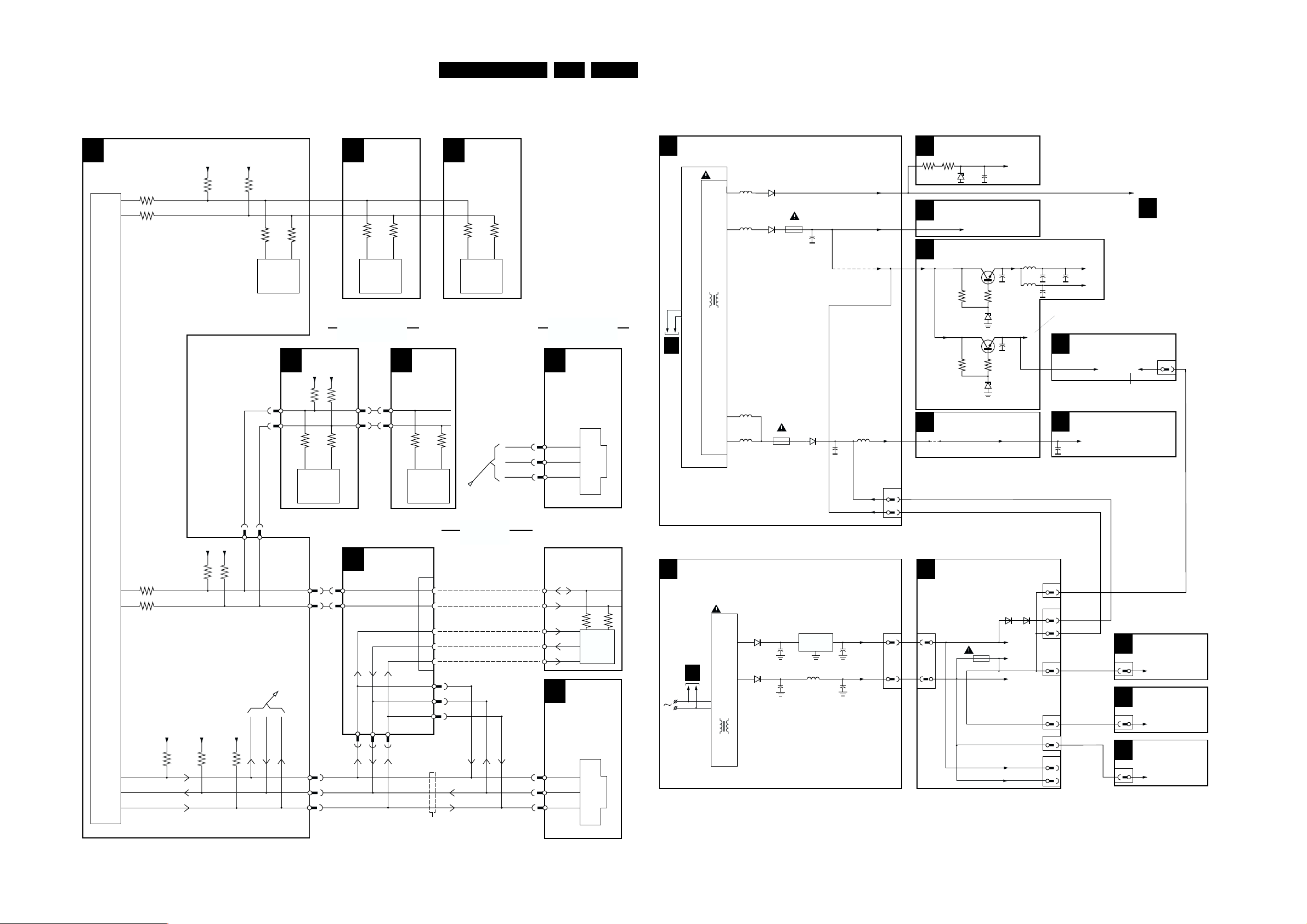
Wiring diagram, blockdiagram, supply diagram and testpoints
22L9H.2E 6.
I2C bus
IIC BUS INTERCONNECTION DIAGRAM
CONTROL
A7
7600
µC
+5VD
3622
50
3623
49
3624-C4
SDA
SCL
3624-C5
+5VD
3626
56
EEPROM
1-0237
2-0237
3625
7601
H1
3811
RADIO
+5VE
3919
3810
15 14
7904
PCF8574A
I/O
EXPANDER
A5
3001
RADIO CLOCK
+5VE
3918
1-0247
2-0247
TUNER +
VIDEO/IF
3000
54
1000
TUNER
G1
1-DP1
2-DP1
3956
CLOCK
DISPLAY
3955
23 24
7951
SAA1064
LED-DRIVER
VIDEO
A6
PROC.
3248783247
7250
TD8844
VIDEO
PROC.
a
4-0238
3-0238
1-0238
CLOCK
(NON SYSTEM)
SP/LS Vbat
H1
1950
SMART
PLUG
1Clock
2
Data-in
Data-out
5
Supply voltages
SUPPLY VOLTAGE DIAGRAM (FOR SYSTEM SETS)
POWER SUPPLY
A1
5545
14
13
POWER
TRAFO
SMPS
F
10
11
(PRESENT FOR
2W/3W AUDIO)
6550
5550
5570 (PRESENT FOR IN AUDIO)
5572
VBATT (MAIN SUPPLY 95V)
6560
1572
800mA
1571
T1.6A
6570
2561
PRESENT FOR
SYSTEM SETS)
MAIN AUX
V
AUX
4510
(4510 NOT
2571
5571
AUDIO
SUPPLY
10V/14VA
0241
1
5
TUNER + VIDEO IF
A5
3002
3003
6007
-/C33
LINE DEFLECTIONA2
MAIN AUX
A7
V
AUX
A5
9507
To 3435
CONTROL
3601 3600
V
AUX-1
3602 3603
TUNER + VIDEO IF
AUDIO SUPPLY 10V/14VA
TO (9-1000)
TUNER
2008
5601
3.3VD
7602
2600 2604 2605
5602
6600
-/3V9
7612
2601
6601
-/3V9
2606
FOR SYSTEM SETS ONLY USED
FOR µC AND NVM SUPPLY
+5D
FRONT CONTROL
A8
SMART SOUND + MONO
A10
SOUND AMPLIFIER
2955
HORIZONTAL
DEFLECTION
(SEE DIAGRAM
FOR NON SYSTEM
SETS)
3V3A
3V3B
+5VD +5VD
FOR SYSTEM SETS ONLY
AUDIO SUPPLY 10V/14VA
TO
A2
0259
3645
52
3644
51
+5VD +5VD +5VD
3616-I10 3617-D5
CLOCK
9
D-IN
17
D-OUT
18
SDA2
SCL2
+5VD+5VD
3624-B3
3624-A2
3617-C4
a
1-0237
2-0237
4-0238
3-0238
1-0238
SMART CARD
J
INTERFACE
1-1237
2-1237
3-0238
4-0238
32-pole
SMART
2-0238
15 SDA2
14 SDL2
PLUG
7
8
9
4-1238
3-1238
2-1238
ONLY FOR
BASIC
SYSTEM
CLOCK
DCM DATA
TV DATA
4-0238
3-0238
1-0238
SMART CARD
µC ON
SMART
CARD
SMART
I
LOADER
SMART
PLUG
1Clock
2
Data-in
Data-out
5
CL 06532004_004.eps
130100
FOR SYSTEM SETS ONLY
EPS (EXTERNAL POWER SUPPLY)
F
T1
CR2
B
A1
POWER
TRAFO
CR1
C
IC4
2
STABILISER
C11 C35
1
L5
C21 C23
+12V
3
1
0228
SMART CARD INTERFACE
J
0228
3
1
1700
250mA
6711 6712
+12Veps
+5Vchas
+5Veps
+5Vchas
+5Veps
+12Veps
+5Veps
0259
0241
1
5
1237
3
0259
1
0237
3
1800
3
10
DCM
CONNECTOR
CONTROL
A7
0237
3
+5VD
SP/LS
I
0259
1
+5V
CLOCK DISPLAY
G1
0259
3
+5V
CL 06532004_002.eps
100100

Wiring diagram, blockdiagram, supply diagram and testpoints
Supply voltage
SUPPLY VOLTAGE DIAGRAM
POWER SUPPLY
A1
5545
6550
5550
14
13
POWER
TRAFO
SMPS LOT
(PRESENT FOR IN AUDIO)
5570
10
5572
11
(PRESENT FOR
2W/3W AUDIO)
VBATT (MAIN SUPPLY 95V)
6560
1572
800mA
1571
T1.6A
0255
1
MAIN AUX
2561
V
*
AUX
4510
NOT PRESENT
*
IN "RADIO" AND
"SYSTEM" SETS
6570
2
0241
3
2571
4
5571
SUPPLY
10V/14VA
5
AUDIO
TUNER + VIDEO IF
A5
3002
3003
6007
-/C33
LINE DEFLECTIONA2
MAIN AUX
A7
CONTROL
V
AUX
TUNER + VIDEO IF
A5
9507
V
AUX-1
To 3435
3601 3600
3602 3603
AUDIO SUPPLY 10V/14VA
7602
7612
2008
6600
-/3V9
6601
-/3V9
TO (9-1000)
TUNER
5601
3.3VD
2600 2604
5602
2606
+5D
2601
23L9H.2E 6.
3V3A
2605
3V3B
FRONT
A8
CONTROL
+5VD
SMART SOUND + MONO
A10
SOUND AMPLIFIER
AUDIO SUPPLY 10V/14VA
2955
+5D
1
0259
A2
SUPPLY 95V
FOR BASIC SETS
SP/LS
I
0259
1
+5V
HORIZONTAL DEFLECTION
MAIN
2552
5551
2409
ON to
A2
3400
3431
3433
6431
5445
2
7
EHT
FOCUS
VG2
3416
6409
9 filement
ON to
6402
5
6
6410
4
9403
9403
3417
+160 160V
2413
A2
6406
6418
2410
2414
0220
3
2
V
LOT AUX
ON to
A2
C-6406
-13V
ON to
A2
A-6403
V
LOT AUX
13V
5V
CRT
B
EHT
FOCUS
VG2
0244
A3
0240
4
A5
A13
ANODE CRT
FOCUS
VG2
3
3349
2
TO CRT
FILEMENT
3350
VERTICAL DEFLECTION
V
LOT AUX +
13V
TUNER + VIDEO IF
7010
LM7805
1
3
+5VA
2
REAR I/O SCART
3316
3326
3336
-13V
C-7312
C-7322
C-7332
to 2-7460
to 4-7460
to (6-1000)
TUNER
+5VA
RADIO + SP/LS + Vbat
H1
OR SP/LS + Vbat
0244
1
2
3
4
5
LM7805
I
1920
7520
O
Vbat (for radio tuning)
+5E
+5E
3
0247
CLOCK DISPLAY
G1
0247
3
+5V
SYNCHRONISATION
A4
5405
VIDEO PROCESSING
A6
SMART SOUND + MONO
A10
SOUND AMPLIFIER
REAR I/O SCART
A13
V
LOT AUX
V
LOT AUX
V
LOT AUX
V
LOT AUX
3411
6412
3
2415
TUNER + VIDEO IF
A5
8V
3207
8V
8V
8V
ON to
2207
V
LOT
C-6400
8V
A2
V
LOT AUX
8V
+8VA
(BIMOS SUPPLY)
SYNCHRONISATION
A4
+8VA
CL 06532004_003.eps
130100

Wiring diagram, blockdiagram, supply diagram and testpoints
Blockdiagram
24L9H.2E 6.
REAR I/O SCART
A15
CVBS_TERR
A5
A6
A6
A6
OUT L (MONO)
A5,A10
A10
RADIO-SP/LS-Vbat
H1
0255
3
5
Vbat
1
0237
SDA2
196
211
SCL2
TUNER / IF / VIDEO DETECTOR
A5
VLOT
AUX+5V
ERR
1000
I6 I5
SDAA7
A7 SCL
POWER SUPPLY
A1
0231
150-276V SINGLE RANGE
7520
MC44603A
OSC
2.5V
14
HOT
GROUND
EPS (EXTERNAL SUPPLY)
F
SCART 1
21
19
17
EXT1R
15
13
11
EXT1G
9
EXT1B
7
5
AUDIO
3
1
AUDIO
OUT R
FOR SP/LS SEE
Vbat
7920-LM7805
1920
RADIO
7904
PCE8574A
I/O
EXPANDER
7010
L78M05
2
11
TUNER
49
5
1500
T 4 AL
1
BUFFER
CURRENT
SENSE
4
VBATT
3540
ADJ
A5
6
31
5500
5501
P3
3935
7
M
1
33V
3
7
8
3520
2
3528
20
18
16
14
12
10
8
6
4
2
6007
-/33V
1901
TUNER
11
6502:6505
EXT1VIDEO
EXT1FB
P4SCART
FRONT EXT1
FRONT EXT1/
AUDIO R
I
+5VE
8
FM
I1
RF-AGC
3002
-
AC
3538
6925
BZX79C12
7903
TDA1308
2
DC
2540
2537
A6
A6
A7
A5
A5
3525
SP/LS
I
SMART PLUG
LOADER
BATHROOM SPEAKER
CONNECTION
7
7250-A
TDA
8842
1003
48
49
38,9
54
VBATT A1
P1
2508
P2
G
7518
STP6NA60
3518
1
6540
2
6537
IC1
CONTROL
1
U1
Clock
Data-in
+5V
Data-out
Ground
IR-data
RJI1
7901
HEF4053B
2
1
IF
5545
D
S
P11
IC2
TV
VIDEO
14
16
13
15
10
11
12
T1
1
2
3
4
5
6
DET
15
V
LOT AUX 8V
5573
PRESENT
2X2W
5570
5572
PRESENT
1X2W
GR2
GR1
0264
SMART CARD INTERFACE
J
32 PIN
0238
1
2
3
4
5
6
J3
1
2
4
2
1
A9
IF
2
3207
+8VA
12
3204
7266
6
I2
3206
6550
5550
1572
6560
800mA
1571
T1.6A
+5Vchas
IC4
SMART CARD
CONNECTOR
VIDEO
AUDIO
IIC2
RESET
RESET FOR
µC ON A7
Spk +
Spk -
0241
INTERFACE
CIRCUITS
Vaux
3
RESET
FORMER
AM MONO DEMODULATOR (FOR BG/I/LL'ONLY)
EXT AUDIO
1701
2561
6570
2571
+12Veps
7705
TDA 9830
16
A1
VIDEO OUT
5202
1200
5.5MHz
CVBS_INT
1201
6MHz
P4
MAIN SUPPLY 9.5V
P5
4510 NOT PRESENT
IN SYSTEM SETS
4510
P4
5571
0241
1
2
3
4
5
0228
+12V
3
2
+5V
1
SOUND
AM
DEM.
A2
SIF
A5
A12
+VBATT
MAIN AUX
V AUX
(µP SUPPLY)
AUDIO SUPPLY
10V/14V
From
0241
J
(SMART CARD
INTERFACE)
To
0228
J
6
7703 7704
A6
CVBSTXT
A7
EXT1
VIDEO
A13
V1
A4
HFLYBK
A2
ABL INFO
A2
HEW_PROTN
A2
G1
SDA
SCL
9
7
8
3710
AUDIO MONO
VIDEO PROCESSING
7256
7250-B
TDA8844
17
13
SYNC
7250-D
TDA8844
SYNC
41
S1
CLOCK DISPLAY
7951
SAA1064
23
LED DRIVER 4x LED
24
MONO
A15
FM, AM EXT.
FM AUDIO
MONO
A5
A12
A12
EXT2
EXT2C
38
10 11
VIDEO OUT
CVBS
Y/C
SWITCH
35 34
1205
4.43
G
50kHz
50
3423
VIDEO/Y
5205
16kHz
E/W
VERT.
DRIVE
SMART SOUND + MONO AMPLIFIER
A10
(ONLY MONO SETS)
7951:7955
A9
SMART
SOUND
MONO
BASS
TREBLE
FRONT HEADPHONE
A11
AUDIO FM DEMODULATOR
A5
(ONLY FOR MONO SETS)
4,5 MHz
1001
5,5 MHz
6,0 MHz
SIF
1002
A5
6,5 MHz
Y-DELAY
R-Y
PAL/NTSC
SECAM
B-Y
DECODER
1208
3.579
+8VA
37
H-DRIVE
G
A7
40
S2
45
S4
47
46
S3
-
DELAY
7953 TDA 7052B (2,3,4 W)
7954 TDA 7056B (1W)
3
A3
7250-A
TDA 8844
FM
AUDIO
DET
I3
A7
V2
V3
28
Y
V4
29
U
30
V
EXT1B
EXT1R
EXT1G
A12
HORIZONTAL DEFLECTION
A2
5551
VBATT
3400
7400
L1
BF422
H-DRIVE µC
A7
HFLYBK
A4
VERTICAL DEFLECTION
A3
VDRIVE-
VDRIVE+
3461
3462
VLOT AUX +11V
F1
BASE
BAND
1
6
A5
8
A4
VOLUME
MONO
HP
7250-C
TDA 8844
27
31
32
23 24 25 26
EXT1FB
5444
TDA9302H
F2
2
RGB
MATRIX
RGB
INPUT
R G B
R-TXT OSD
24092551
7402
BU1508DX
L2
3404
7460
A7
I4
A7A7
SCL
V9 V10
7
R
CONTROL
G
CATHODE
B
CALIBRA-
6212
B-TXT OSD
G-TXT OSD
FB-TXT OSD
A7
6460
2
7
+
OP. AMP
1
-
3407
15
EXT AUDIODUAL / MONO
SDA
8
RGB
TION
22
L3
6
4
MONO
A10
A15
ERR5ERR
+
R
G
B
18
V8
6434
6404
3405
6461
2464
3
VLOT AUX
-13V
6
21
20
19
5
FRONT
A8
CONTROL
6680
LTL-307 X
7680
GP1U 280P
LOCAL
KEYBOARD
FOR SYSTEM SETS
J
Vaux
7605
uPreset
FORMER
FOR NON SYSTEM SETS
BCL_PROTN
HDRIVE
A4
7607
NE555D
LINE
63
DRIVE
START UP
CIRCUIT
HDRIVE µC
A2
V5
0243 0245
V6
V7
ERR
12
ABL INFO
A2
6409
0221
2440
3406
F4
V_GUARD
F5
0 222
1
F5
2
3401
LED
A7
IR RECIEVER
RC5
A7
7611, 7620, 7621
PROT.
CIRCUIT
7608
B
1
2
3
4
5
6
+160V
3416
2413
A7
VERT.
DEFL.
COIL
RESET
HORDEFLCOIL
A7
A10,D2
A7
A7
CRT
V11
V12
V13
BLKCURINFO
+160
2
7
1
CONTROL
BUZZER (N.A)
VOLUME +
W_DISABLE
A7
BASS
A10
DUAL/MONO
A5
EXT 1/2
A5
TREBLE
A10
SCART PIN8
A13
0605
A13
RF/VIDEO 2
SWITCHING
KEY BD 1
KEY BD 2
KEY BD 3
STANDBY
A5
LED
A8
AV MUTE
A13
CVBS TXT
A6
7311:
-
7313
0244
0220
5445
10
11
12
13
14
15
16
17
18
19
20
21
22
23
24
25
26
3316 3326 3336
7321:
-
7323
7331:
-
7333
FILEMENT
3 2 1
FOCUS VG2
8
6402
5
3409
6410
11
6412
3
3411
10
9
6405
6403
6406
3412
1
2
3
4
5
6
7
8
9
7600
SAA
CVBS
3417
µC
ERR
P2
P3
ERR
8
HSYNC
P0
R
G
B
VLOT AUX 13V
+
ERR9ERR
+
10
7601
EEPROM
4
7
52
51
C2
50
7
49
P1
48
47
46
45
44
C4
43
RESET
42
41
40
39
38
37
VSYNC
36
35
VDS
34
R
33
G
32
B
31
30
29
28
27
V14
V15
V16
3415
2410
2414
L6
2415
L7
2417
2411
+160V
7401
PROT
CIRCUIT
L4
L5
R
G
B
+3V2
C1
+3V3
SDA
SCL
33503349
C3
SYS1/AM
VD
HD
FB_TXT_OSD
R_TXT
G_TXT_OSD
B_TXT_OSD
LLP\M TRAP
G2
V
BCL_PROTN
ABLINFO
VLOTAUX 13V
VLOTAUX 5V
A3
VLOTAUX+8V
FILEMENT
VLOTAUX+13V
6415
HEW_PROTN
CL 06532004_001.eps
W_DISABLE
SDA
SCL
VD
RC5
RESET
X - TAL
12MHz
7609
V-GUARD
7608
OSD
_
0267
1
2
3
V FOCUS
ERR
2
A5,A6,D1
A5,A6,D1
A9
A8
A7
ERR
HFLYBK
A6
A6
A6
A6
A5
FOR
COMPAIR
CRT
25kV
EHT
A7
A4
A4
130100
A7
3
A3
A2

Wiring diagram, blockdiagram, supply diagram and testpoints
25L9H.2E 6.
Waveform Overview
P1
50V / div DC
5ms / div
P1
300V DC
P3 15V DC
P3 13V DC
9V5 DC
P4
95V DC
P4
P5 9V5 DC
P5
8V DC
P6 17V DC
P6
15V DC
P2
2V / div DC
10µs / div
P2
2V / div DC
10µs / div
L1
L3
100V / div DC
L3 0V DC
SDM
L4
L4
L5 8V DC
SDM
L5
L6 8V DC
SDM
L6
L7 -13V DC
SDM
L7 -0V2 DC
F1
F2
F3
20µs / div
13V DC
0V1 DC
0V2 DC
2V DC
0.5V / div DC
5ms / div
0.5V / div DC
5ms / div
S2
1V / div DC
20µs / div
S3
1V / div DC
5ms / div
S4
1V / div DC
5ms / div
I1
0.2V / div DC
5µs / div
I3
1V / div DC
5µs / div
I4
V7
0.5V / div AC
20µs / div
V14
50V / div DC
20µs / div
V15
50V / div DC
10µs / div
V16
50V / div DC
10µs / div
C1
1V / div DC
0.5µs / div
C4
A3d
1V / div DC
0.5ms / div
A20 1V5 DC
A21
0.5V / div DC
0.5ms / div
A22
0.5V / div DC
0.2ms / div
A23 SCL uP
1V / div DC
10µs / div
A24 SDA uP
Testpoint overview
MAIN PANEL COMPONENT VIEW
13
0267
17
AUDIO PANEL
02390240
1
COMPAIR
A3
4
2
7954
5
6
A5 A4
7953
1
8
EEPROM
1
8
V3
V4
S2
S1
S3
S4
A3
A5
A4
7601
4
5
7250
TV PROC.
29
30
40
41
46
47
56
28
21
20
19
18
15
1
3
6
8
9
0232
7680
C5
31
7600
uC
27
26
42
C1
43
C4
49
C3
50
C2
52
1
V2
V5
V6
V7
V8
l4
8
V10
7
V9
6
I1
1
l3
3212
L1
V1
9636
9633
P4
9234
SDM
0225 0226
SDM
1572
6550
HOT GROUND
BORDER
P6
6570
P5
6502
7518
SDG
P3
0231
2
4
1500
P2
1
7520
8
P1
16
9
1
3
VBATT ADJ
L2
L3
7402
2508
95V
3540
B
C
E
1V / div DC
20µs / div
L1
1V / div DC
20µs / div
L2
2V / div DC
20µs / div
0V DC
L2
10V / div DC
5ms / div
F4 V2
2V / div DC
5ms / div
F5
V5
0.5V / div DC
5ms / div
S1
V6
1V / div DC
20µs / div
1V / div DC
2µs / div
0.5V / div AC
20µs / div
0.5V / div AC
20µs / div
0.5V / div AC
20µs / div
1V / div DC
5µs / div
C5
1V / div DC
5µs / div
A1
10mV / div AC
5µs / div
A3b
1V / div DC
0.2ms / div
1V / div DC
20µs / div
= 0V
CL 96532028_053.eps
210499
17
1
1000
TUNER
11
5
4
I1
I6
I5
CRT PANEL (COPPER TRACK VIEW)
1
0244
9
4
10
B
V16
11
12
CRT
SOCKET
V13
R
V14
8
G
7
V15
6
G
V12
V11
16
R
B
5
0245
3417
F4
6461
L6
3411
L7
6405
9403
LOT
FOCUS
VG2
L4
CL 06532044_010.eps
100100
L5
F5
F1F3F2
7460
7 1
3465
3466
652

Schematics and PWB’s
7. Schematics and PWB’s
Power supply
26L9H.2E 7.
A
FOR NON SYSTEM SETS
150 - 276 V SINGLE RANGE
90 - 276 V FULL RANGE
B
FOR SYSTEM SETS
C
(EPS, EXTERAL
POWER SUPPLY)
D
E
F
G
H
12345678910
POWER SUPPLY
MAINS
To
0211
F
DEGAUSSING COIL
Not used
0212
B2P3-VH
0211
0213
2520
82p
3524
2531
560p
3536
39K
3532
6K8
2532
RES
2533
330p
3534
220K
1
1
2
9500
0231
2
2
4
1
9501
4M7
3542
2M2
3502
2
1
7520
MC44603A
82K
3520
Vdem in
8
0V3
9 2
Sync
C
2V6
T
10
(2V6)
R standby
15
F
(2V5)
2V5
R standby
12
P
0V7
(1V7)
2.5V
14
VOLTAGE
2V5
FEEDBACK
(2V5)
13
E/A OUT
3V2
(2V2)
1n
2534
FOLDBACK INPUT
2504
SDKE
1
3
5689
DEMAGNETICATION
MANAGEMENT
Vdem out
Iref
OSCILLATOR
(REDUCED FREQUENCY)
ERROR
AMP
FOLDBACK
3512
15K
2n2
3504
2
9504
2501
33n
1500
T4A
3537
10K
Rref
Vosc prot
Vosc
Iref
STANDBY
CURRENT SENSE INPUT
5
1V1
5521
2U2
3513
220K
3
6501
3501
470R
2500
220n
2506
2V5
(2V5)
16
Vref
REFERENCE
BLOCK
2522
2n2
BZX79-C30
470n
Iref
Vref
enable
7
2521
6500
3505
DSP
5501
DMF-2820
5500
DMF-2405
6510
BZX79-C20
2529
100n
CURRENT
SENSE
Dmax & SOFT-START
Iref
2n2
+t
ZPB
3503
23
14
23
14
3510
3530
3529
INITIALIZATION BLOCK
Latch
Reset
THERMAL
SHUTDOWN
CONTROL
33K
3K9
4R7
SUPPLY &
QSet
2530
3506
2R2
3547
B57237
Vovp out
Soft Start & Dmax
11
2V4
(2V4)(1V)
1u
2505
2502
t
BUFFER
Vref
OVERVOLTAGE
MANAGEMENT
2n2
1N5062
2n2
1N5062
P3
Vcc
UVLO1
OUTPUT
Vcc
OVERVOLTAGE
PROTECTION
UVLO1
Vref
6504
6503
9506
3548
B57237
5552
GND
t
100MHZ
(13V2)
14V
1
18V
Vc
(12V7)
13V
3
1V2
4
6
(2V)
9503
6502
1N5062
6505
1N5062
3525
33R
5502
2524
6507
6508
470p
3528
BYD33J
BYD33J
2517
330R
150R
P2
1n
3521
1V2
3517
6520
6521
2540
3539
3540
309V
2508
220u
7518
STP6NA60
G
S
0V
10K
1N5062
1N5062
2590
330p
6540
BAV21
100u
3538
100K
18K
4K7
VBATT
ADJ
2511
D
3519
(318V)
308V
470R
220u
2518
3518
P1
5516
100MHZ
470p
R27
100n
2537
P1
50V / div DC
5ms / div
3509
2509
2510
5540
4U7
6537
BAV21
G5P
1580
23
FOR USA ONLY
100R
5545
2084
7
820p
820p
4
1
2
47R
3541
4n7
2541
2545
1n5
EAR
P1
P3 15V DC SDM
P3 13V DC
P4 9V5 DC SDM
P4
14
14
16
13
15
10
11
12
MainSupplyGnd
300V DC
95V DC
6585
BAS216
13V
7591
BC847B
F01
TO SIN OF
P5 9V5 DC SDM
P5
P6 17V DC SDM
P6
3598
22K
6584
5573
*
100MHZ
*
100MHZ
8V DC
15V DC
BAS216
100MHZ
BYV27-200
5570
5572
2572
Europe Only
7590
BC847B
2560
1n
6560
3570
100p
0V7
123456789
10K
3597
100MHZ
2565
1572
800mA
1571
T1.6A
10R
P2
2V / div DC
10µs / div
3595
3596
10K
5550
220p
MP
1m
2561
SignalGnd
6570
EGP20DL
2570
2n2
AudioSupplyGnd
10 11 12
VlotAux13V
68K
6590
BAS216
220u
2586
6550
21
BY229X-600
2550
1n
NOT PRESENT
IN SYSTEM AND "RADIO"SETS
4510
18V
2571
P2
2V / div DC
10µs / div
11 12
2509
2510
3528
7518
P4
95V
0255
2
1
(RADIO-SP/LS-Vbat)
P5
9V5
0241
5
4
3
9V5
2m2
(RADIO-SP/LS-Vbat)
2
1
5571
10u
P6
AUDIO O/P
*
2W/3W
5570
5572
1W
...V... Normal Operation
(...V...) StandBy Operation
20/21" 14"
820p
820p
220
6NA60FI
VBatt
MainSupply95V
TO PIN 1-2
OF 0255
0241
H1
MainAux
Vaux
TO PIN 3,4,5
OF 0255
0241
H1
AudioSupply10V|14V
HOT GROUND
CL 06532004_012.eps
1n
1n
270
4NA60FI
TO
0241
OR
J
(SMART CARD
INTERFACE)
130100
C
D
G
H
F01 F9
0211 C2
0211A C2
0211B C2
0212 A2
0213 D2
0231 B2
0241 D11
0255 C11
1500 B3
A
1571 E10
1572 D10
1580 A8
2500 C3
2501 B3
2502 B5
2504 A3
2505 B5
2506 C3
2508 B6
2509 C7
B
2510 C7
2511 B7
2517 C6
2518 C7
2520 E2
2521 H4
2522 H3
2524 F6
2529 D4
2530 H4
2531 E2
2532 F2
2533 G2
2534 G2
2537 F7
2540 E6
2541 F7
2545 G8
2550 C10
2560 C9
2561 D10
2565 C10
2570 E10
2571 F10
2572 F9
2586 A10
2590 E7
3501 B3
3502 C2
3503 A4
3504 A3
3505 B4
3506 B5
3509 B7
3510 C4
E
3512 H2
3513 H3
3517 C6
3518 D7
3519 D7
3520 E2
3521 D6
3524 E2
3525 C6
3528 E6
3529 D4
3530 D4
F
3532 F2
3534 G2
3536 F2
3537 D3
3538 F7
3539 F6
3540 F6
3541 E7
3542 C2
3547 C5
3548 C5
3570 F9
3595 A10
3596 A10
3597 A10
3598 A9
4510 D10
5500 C4
5501 B4
5502 E6
5516 C7
5521 H3
5540 E7
5545 B8
5550 C10
5552 D5
5570 E9
5571 E11
5572 E9
5573 C9
6500 B4
6501 B3
6502 B6
6503 B5
6504 B5
6505 B6
6507 B6
6508 C6
6510 D4
6520 D6
6521 D6
6537 F7
6540 E7
6550 C10
6560 D9
6570 E10
6584 A9
6585 A8
6590 A10
7518 C6
7520 E2
7590 A9
7591 A9
9500 B2
9501 C2
9503 D5
9504 B3
9506 C5

Schematics and PWB’s
Main panel (component side)
27L9H.2E 7.

Schematics and PWB’s
Main panel (copper side)
28L9H.2E 7.

Schematics and PWB’s
Line deflection
29L9H.2E 7.
123456789101112
LINE DEFLECTION
MainAux
3435
CRT_Discharge
A6-63
A3-63
A7-32
A4-32
A7-8
2407 9.1nF 11nF 11nF
2411 1uF 1uF 1uF
2416 NA
2434 NA NA NA
3411 1R
3414 1K8 Jumper Jumper
3415 12K 10K 10K
5401
5404
56uH NA
5406
5408 27uH 27uH 27uH
6434
Jumper Jumper Jumper
9402 NA NANA
9408
9424
9425
14"
2407 8.2nF 10nF 11nF
2411 100uF 100uF 100uF
2416
680pF 680pF 330pF
2434
3411 1R 1R 2R2
3414 1K 1K8 2K2
15K 10K
3415
5401
5404
56 uH
5406
5408 15uH
6434
Jumper Jumper Jumper
9402 NA NA NA
9408
9424
9425
7431
BC857B
Hflybk
HdriveUC
NA 560pF
NA 100uH NA
NA NA Linearity Drum
NA NA
NA
NA
NA NA NA
NA NA
NA NA Linearity Drum
NA
NA
Yes Yes NA
Ye s
NA
20" 21"BRAZIL
56uH NA
15uH 22uH
NA
NA
2432
6432
10V
9V5
100u
L1
21"20"14"
56uH
NA
NA
NANAYe s
10K
NA
NA
Ye s
10K
4435
1N4148
6435
BAS216
3421
100R
5410
5U6
VBatt
MainSupply95V
2431
3434
47K
Vlot8V
6400
1N4148
3404
12K
6401
1N4148
2402
USAEurope
2407
8.2nF 10nF 9.1nF
2411 100uF 100uF 100uF
680pF 560pF 330pF
2416
2434 NA NA NA
3411 1R1R 1R
3414 2K7 1K8 2K2
3415 12K 10K 10K
5401
5404
5408 15uH 15uH 22uH
6434
9402
9408
9424
9425
2407 9.1nF
2411
2416
2434 NA NA NA
3411 1R 1R 2R2
3414
3415 15K 10K 10K
5401
5404
5406
5408 15uH 15uH 22uH
6434
9402 NA NA NA
9408
9424
9425
NA NA NA
56uH 27uH 56uH
NA NA5406
Jumper Jumper Jumper
NA
NA
Yes Yes NA
14" 20" 21"AP
100uF 100uF 100uF
680pF
1K 1K8
NA 100uH NA
56 uH NA NA
NA NA Linearity Drum
Jumper
NA
NA
Ye s
5551
27u
47u
2551
9425
3433
220K
6431
2u2
BAV21
47n
2400
4n7
2406
0V4
75R
330p
3420
1R 2R2
NA
NA
11nF 10nF
680pF 330pF
Jumper Jumper
NA
NA
NA NA
12u
5401
3431
220K
82K
3432
47n
2401
Linearity Drum
3400
5444
31V
7400
BF422
21"20"14"
NA
NA
NA
2K2
NA
Ye s
5406
4K7
3403
5K6
6433
BYD33M
9424
5404
56u
DC12
3402
U10
2403
3407
220R
3405
2405
470p
L2
27R
680p
2416
1n5
2407 11nF
2411 100uF
2416
2434 NA
3411
3414
3415 10K
5401
5404
5406
5408 22uH
6434
9402 NA
9408
9424
9425
2420
4K7
3406
-0V2
7402
BU1508DX
Linearity Drum
2404
560n
4K7
9402
L3
3436
2K2
21"CHINA
NA
2R2
2K2
NA
56uH
Jumper
NA
NA
NA
0221A
0221B
0221C
330n
2434
47n
6434
BYD33D
88V
FISH HOOKS
FOR
BRAZIL ONLY
0221
4
1
VH
3474
22R
6404
BYD33M
6419
1N4148
2409
2407
1N4148
HORIZONTAL
DEFLECTION
COIL
5408
27u
9408
2408
22n
47u
8n2
6418
FILEMENT
+160
1
7
2
6
9
10
3
4
5
6409
BYD33D
5445
AT2078
0220
1
2
3
3416
EHT
8
TO 0224 OF
CRT PANEL
1V / div DC
20µs / div
3R9
22u
2413
TO PICTURE TUBE
TO CRT
VFOC
PANEL
VG2
L1
1V / div DC
20µs / div
+160
2412
6406
1N4148
3414
33n
3415
2K2
4401
15K
6403
2418
470n
6413
BZX79-C12
10K
3423
BAS216
1N4148
3412
1R
L2
2V / div DC
20µs / div
6402
BYD33D
6410
BYD33D
6412
BYD33D
6405
BYD33D
6415
3440
2411
6414
BAS216
10K
1u
3441
3424
9403
3417
3411
9404
3418
150K
1R
1R
22K
6K8
5V7
3419
2410
2414
2415
2417
7403
BC847B
VlotAux13V
7401
BC857B
13V
470u
1m
ITV fish hook
1400
1m
470u
3426
8V7
6V1
47K
6408
L3L1
100V / div DC
20µs / div
13V
3425
100R
1K
10K
3427
BZX79-F6V2
L4
L5
L6
L7
BC857B
7404
2V4
3428
10K
For USA only
L3 0V DCL2 0V DC
L4
13V DC
0V1 DC
L4
L5 8V DC
L5
0V2 DC
BCL_Protn
ABLinfo
VlotAux13V
VlotAux5V
Vlot8V
-13V
Vlot8V
HEW_Protn
L6 8V DC
L6
L7 -13V DC
L7 -0V2 DC
A7-20
A6-62
A4-62
A4-81
2V DC
A
B
C
D
E
F
G
H
0220 F7
0221 B6
0221A A6
0221B A6
0221C A6
1400 D10
2400 D4
2401 D4
2402 E4
2403 E5
2404 B5
2405 D5
2406 E4
2407 D6
2408 C7
2409 C6
2410 C10
2411 F9
2412 C8
2413 A8
2414 D10
2415 E10
2416 D5
2417 E10
2418 B9
2420 B5
2431 C3
2432 D2
2434 C6
2551 B4
3400 D4
3402 D5
3403 E5
3404 D3
3405 B5
3406 B5
3407 B5
3411 D10
3412 F9
3414 B8
3415 B8
3416 A8
3417 D10
3418 F10
3419 F10
3420 E4
3421 E3
3423 B9
3424 B10
3425 C10
3426 F10
3427 F10
3428 F11
3431 C4
3432 D4
3433 C4
3434 C3
3435 C3
3436 E5
3440 F9
3441 F10
3474 C6
4401 B9
4435 C3
5401 B4
5404 B5
5406 B5
5408 B6
5410 E3
5444 D4
5445 B7
5551 B4
6400 D3
6401 E3
6402 C9
6403 F9
6404 D6
6405 E9
6406 F8
6408 G10
6409 A7
6410 D9
6412 D9
6413 B9
6414 B9
6415 E9
6418 E6
6419 E6
6431 C4
6432 C3
6433 B5
6434 C6
6435 C3
7400 E4
7401 B10
7402 D5
7403 F10
7404 F11
7431 C2
9402 B5
9403 C10
9404 E10
9408 C6
9424 B5
9425 B4
123456789101112
CL 96532028_036.eps
070499

Schematics and PWB’s
30L9H.2E 7.
Frame deflection
123456
FRAME DEFLECTION
A
B
C
D
CRT_Discharge
E
Europe
V_Guard
A7-31
VdriveNeg
A4-64
VdrivePos
A4-65
A2-63
3465
3466 5R6 4R7 4R7
F4
3469
3461
1K
2K2
3460
3472
2K2
14" 20" 21"
5R6 4R7 3R3
6461
BZX79-C33
VlotAux13V
10K
2463
F1
2460
470p
2461
F2
2462
1K
3462
0V
4n7
2470
3471
390R
3465 5R6 3R9 4R7
3466 5R6
1V
3470
820p
1V
470p
3473
18K
100n
7460
TDA9302H
1V
1
7
100R
7469
BC847B
14" 20" 21"USA
IN-
IN+
-13V
POWER
AMPLIFIER
6460
BYD33D
13V
2
VSUP6VSUPO
GND
4
100n
2465
3R34R7
2464
100u
-13V
3
FLYB
FLYBACK
GENERATOR
THERMAL
PROTECTION
3463
1R5
3464
2K2
OUT
Synchronisation
0222 C5
0222A C5
0222B C5
2460 C2
2461 C2
2462 C2
2463 B3
2464 B4
2465 D3
2466 C4
2467 C5
A
2470 E2
3460 C2
3461 C2
3462 D2
3463 D4
3464 D4
3465 D5
3466 D5
3467 D5
3468 C5
3469 B2
3470 B3
B
3471 E2
3472 D2
3473 D3
6460 B3
6461 B2
0222B
FISH HOOKS
FOR
0222A
BRAZIL ONLY
F3
0V5
5
220n
2466
3468
220R
3467
220R
2467
100n
F5
0222
1
2
VERTICAL
DEFLECTION
COIL
7460 B3
7469 D3
C
D
A
B
C
D
4R7
4R7
3466
3465
E
E
123456
SYNCHRONISATION
+8VA
Hflybk
A2-32
2237
100p
3268
33K
2238
15p
2233
S1
3271
1u
4M7
3266
15K
2239
4V2
3270
4M7
100n
3V8
2234
0V7
3269
7250-D
TDA8842
43
4n7
41
51
52
4V
39K
PH1LF
FBISO
VSC
I_REF
VlotAux8V
3265
1M
2n2
2231
42
37
3V
8V
V_P2
PH2LF
VDRA46VDRB
1V4
1n
2240
2241
CL 96532028_040.eps
S3
S4
1K
3276
2232
47
1V4 2V4
1n
070499
3274
2n2
HOUT
DECDIG
EWD
GND2
EHTO
50
1K
2243
5205
2244
40
2V3
39
5V
45
0V2
44
VlotAux8V
220n
22u
3272
3273
100u
VlotAux8V
S2
2242
27K
3275
220K
10K
10u
2255
100p
2236
220n
AVL
5405
27u
2235
Vlot8V
Hdrive
1n
XRAY_Protn
ABLinfo
A7-7
A2-81
A2-62
A
B
C
D
E
2231 C3
2232 C4
2233 C2
2234 C3
2235 D5
2236 C5
2237 D2
2238 E2
2239 E2
2240 D4
2241 D4
2242 D5
2243 E4
2244 C4
2255 C5
3265 B4
3266 C2
3268 D2
3269 D3
3270 E3
3271 E2
3272 E5
3273 E5
3274 E4
3275 E5
3276 E4
5205 B4
5405 B5
7250-D C3
F
14" 20" 21"Brazil
3465 5R6 4R7 3R3
3466 5R6 3R9 4R7 3466
G
AP 21"20"14"
3R34R76R83465
4R7 3R35R6
F
F
StereoMono
1nF
2235
1nF--
2242
VdriveNeg
VdrivePos
A3-64
F
A3-65
G
G
G
F1 F2 F3 F5F4
H
0.5V / div DC
5ms / div
0.5V / div DC
5ms / div
10V / div DC
5ms / div
2V / div DC
5ms / div
0.5V / div DC
5ms / div
CL 96532028_037.eps
H
H
070499
S1
1V / div DC
20µs / div
123456
1
S2 S3 S4
H
1V / div DC
20µs / div
1V / div DC
5ms / div
1V / div DC
5ms / div
CL 06532004_013.eps
110100
23456

Schematics and PWB’s
Tuner video IF
1
TUNER, VIDEO IF, VIDEO DET, FM-AUDIO DET.
SCL
A5-25
A7-25
SDA
A5-24
A7-24
FM|AM|ExtAudioMono
A9-37
ExtAudioMono
A9-38
A13-38
LLp|Mtrap
A7-23
LLp|F1
A9-39
LLp|F2
A9-40
*
3031
4K7
234567891011
1000
12
13
MT
14
15
AS
3000
100R
3001
100R
1012
1011
1010
VlotAux8V
3029
*
7001
*
BC847B
1K
3033
3
I5
For EMC shield
2K2
6008
BAS216
**
5V
*
VBatt
SCL5SDA
4249
*
3032
0V7
3034
TUNER
4
I6
F02
SIN
6009
7002
*
22K
BC847B
1K
3002
15K
+58ADC
from SIN of
3030
BAS216
*
31L9H.2E 7.
F02 C3
9000 B6
0239 A11
9203 G6
0240 A9
9204 E4
1000 B2
ONLY USED FOR MECHANICAL FIXATION OF "RADIO -SP/LS-Vbat" PANEL
##
Dual|Mono
3021
#
3208
220R
A7-6
1K
4215
4221
3209
VlotAux8V
3003
13
2252
100n
2003
6003
6004
3013
10K
3015
3
1005
OFWK6272K
SWI
IN
ING
GND
38
7010
L78M05
2
3014
100u
3016
680R
100K
4
5
O1
O2
18K
4
5
2004
3277
3278
#
1K
1K
2227
2200
22n
2V4
4V7
49
48
2
470n
1n
2208
#
+5VA
IFIN2
IFIN1
AUDIOEXT
4201
1V5
7254
#
BC847B
*
220n
#
12K
2008
6007
BZX55-C33
1
1V6
2
6
5V
NC
9
34V
10
11
7
I1
820n
5004
*
4000
*
4001
6K8
3027
*
2012
*
10n
2K2
2K2
3028
*
#
#
*
*
9204
4218
4248
10u
2001
4247
VlotAux5V
47n
2002
1
2
*
BAS216
*
BAS216
*
10u
1003
*
*
10
1
2
1V
54
AGCOUT
2201
3226
330K
53
4V4
1u
#
3V2
IntCarSIF
#
#
1N4148
#
1N4148
2K2
3018
2005
100p
##
IFDEM13IFDEM2
7250-A
TDA8842
DEC_AGC
AUDEEM
DECSDEM
55
56
4V7
4V7
33p
2202
2203
##
+5VA
3K3
3227
2209
220n
220R
0V9
3229
#
9000
6005
6006
4
10u
#
AUDIOOUT
15
3200
#
3017
3V4
I4
680R
4K7
#
3020
22K
I3
112
V_P1
SNDIF
GND1
IFVO
PLLLF
5
2V9
390R
3201
2205
100n
4200
#
9203
AudioSupply10V|14V
3V1
#
7000
BC847B
VlotAux8V
3R3
3207
100n
2206
2207
100u
14
I2
3205
6
1K
1M
3202
*
#
9220
#
9205
#
#
+8VA
2220
7266
BC847B
EGP20DL
6216
9279
1001
SFSH
1
1002
SFSH
1
100n
2
2
3204
8V6
3206
AudioSupply10V|14VA
3
#
2006
47p
3
100R
4210
4222
2256
220n
4223
#
2V6
560R
SDA
A5-24
SCL
A5-25
AudioOutL|Mono
A13-41
AudioOutR
A13-42
Ext2AudioL|Mono
A5-43
A13-43
A13-44
A5-45
A9-45
1K
Ext2AudioR
VlotAux8V
+5VA
FM|AM|Audio
5202
*
6u8
1200
*
TPS
1I3
O
G
2
1201
*
TPS
3
I1O
G
2
# SEE DIVERSITY LIST FOR A5
0240
1
2
3
4
5
6
7
8
9
10
11
12
13
14
15
16
17
3216
470R
3212
470R
3213
470R
I1 I3 I4
0.2V / div DC
5µs / div
1V / div DC
5µs / div
SIF
A5-46
Front|Ext1AudioL
A11-47
Front|Ext1AudioR
A11-48
Volume
A7-3
Buzzer
A7-2
MainAudioL|Mono
A10-49
AudioSupplyGnd
AudioSupply10V|14VA
SIF
VideoOut
CVBS_INT
FM|AM|Ext_VC_AudioMono
FM|AM|Audio
AudioOutL|Mono
FM_AudioMono
1V / div DC
2µs / div
A5-46
A13-50
A6-51
A10-37
A5-45
A5-43
A9-53
0239
1
2
3
4
5
6
7
8
9
10
11
12
13
14
15
16
17
CL 06532004_014.eps
130100
A
B
C
D
E
G
G
H
A
B
C
D
E
F
F
H
1001 A7
1002 B7
1003 E4
1005 G4
1010 D2
1011 C2
1012 C2
1200 E9
1201 E9
2001 B4
2002 C4
2003 B4
2004 C5
2005 B5
2006 B8
2008 A3
2012 E3
2200 F5
2201 F5
2202 F5
2203 F6
2205 F6
2206 D7
2207 D7
2208 G5
2209 G6
2220 D7
2227 E5
2252 B4
2256 E8
3000 C2
3001 C2
3002 A3
3003 A3
3013 C4
3014 B4
3015 C4
3016 C5
3017 A6
3018 B6
3020 B6
3021 B8
3027 E3
3028 E3
3029 E2
3030 E3
3031 F1
3032 F2
3033 F2
3034 F2
3200 F6
3201 F6
3202 F7
3204 D7
3205 E7
3206 F7
3207 D7
3208 E8
3209 F8
3212 E9
3213 F9
3216 D9
3226 G5
3227 G5
3229 G6
3277 E5
3278 E5
4000 D3
4001 E3
4200 G6
4201 F5
4210 D8
4215 C8
4218 F4
4221 D8
4222 E8
4223 E8
4247 E4
4248 F4
4249 E2
5004 C3
5202 D9
6003 C4
6004 C4
6005 B6
6006 B6
6007 A3
6008 E2
6009 E2
6216 A7
7000 B7
7001 F2
7002 F2
7010 A4
7250-A E6
7254 G5
7266 E7
9205 G7
9220 G7
9279 A7
1234567891011

Schematics and PWB’s
Personal notes:
32L9H.2E 7.
DIVERSITY TABLE FOR A5
TUNER VIDEO IF (Europe)
*
1003 K3953M G1965M 1005
1200
1201
2012
2014
2201
3013
3027
3028
3029
3030
3031
3032
3202
4000
4247
4248
4249
5004
5006
5202
6003
6004
6008
6009
7001
7002
9207
B/G, D/K SW
-
TPT02 TPT02 TPWA04
- 6MHZTPS 6.5MHZTPS
10 n 10 n Jumper
5p6 2u2
10k 10k Jumper
6k8 6k8 6k8
2k2 2k2 2k2
2k2 2k2 2k2
2k2 2k2
4k7
22k 22k -
- - 1M5
Jumper Jumper 10n
Jumper Jumper
-
- - Jumper
0u22 0u82 0u82
78MHzVCO - -
3u3 3u9
Bas216
Bas216 Bas216 -
BA792 BA792 BA792
BA792 BA792 BC847B BC847B BC847B
BC847B
Jumper Jumper
- K6289K
2u2 1u
4k7 4k7
- Jumper
Bas216 -
BC847B -
3u9
G1984M J1980M
TPWA04 6MHZTPS
-
Jumper Jumper
-
Jumper Jumper
Jumper Jumper
-
-
Jumper Jumper
BG ILL’ST LL’MN
--
--
--
--
1u 1u
-
-
--
-
--
--
1M5 1M5
--
--
0u82 0u82
--
6u8 6u8
--
--
-
-
-
--
-
-
-
-
-
-
TUNER SOUND IF (Europe)
#
BG I BG/DK
0239
0240
1001
1002
1204
2005
2006
2202
2203
2208
2209
2227
2245
3017
3018
3020
3200
3226
3227
3229
4202
4218
4221
4223
4283
4284
5204
6005
6006
7000
7254
9000
9203
9204
9205
9220
9253
--
---
5.5 6.0 5.5
- - 6.5
---
100p 100p
82p
3n9 3n9 3n9
10u 10u 10u
220n 220n 220n
Jumper Jumper Jumper
470n
--
- - 4k7
- - 2k2
- - 22k
680R
330k 330k
680R 680R 680R
270R 270R 270R
---
Jumper Jumper Jumper
-Jumper
Jumper Jumper Jumper
Jumper Jumper Jumper
---
- - 1N4148
- - 1N4148
--
BC847C
Jumper Jumper
Jumper Jumper Jumper
---
---
--Jumper Jumper Jumper
Mono
-
100p
82p 82p
470n 470n
-
680R 680R
330k
-
Jumper Jumper
BC847B
BC847C BC847C
-
BG/I/LL’ BG/I/DK
-Yes
-
5.5
6.0
--
100p -
82p 3n9 10u -
220n -
Jumper -
470n Jumper
-4k7 2k2 22k -
680R -
330k
680R
270R
--
--
- Jumper
Jumper Jumper
Jumper Jumper
Jumper Jumper
--
1N4148 -
1N4148 BC847B BC847C -
-
Jumper
Jumper Jumper -
- Jumper
Ye s
-
-
-
-
-
-
-
-
Stereo
BG/I/LL’
Ye s
Ye s
-
-
K9456M
-
-
-
-
-
-
Jumper
4u7
-
-
-
-
-
-
-
Jumper
-
-
-
-
-
1u8
-
-
-
-
-
-
-
-
-
Jumper
CL 96532028_041.eps
070499

Schematics and PWB’s
Video processing
33L9H.2E 7.
1 2 3 4 5 6 7 8 9 10 11 12
VIDEO PROCESSING (EUROPE)
SDA
A7-24
SCL
A7-25
Ext2Video|Y
A13-54
Ext2C
A13-55
CVBSTxt
A7-22
Ext1Video
A11-57
A13-57
CVBS_INT
A5-51
DIVERSITY TABLE
3218
100R
3223
75R
V1
SC1 (Mono)
2212
2213
3224
1208 3.58MhzXtl 3.58MhzXtl 3.58MhzXtl
2211
2248 15pF
3206
3213
3217 6K8
7250 TDA8845N1 TDA8842S1
-
-3228
LL’ST LL’MN
100nF 470nF 100nF 470nF
270R 270R
470R 560R 560R 470R
VlotAux8V
3219
560R
2210
470n
2211
470n
SC1
Front Cinch (Mono)
100nF-
100R
15pF 15pF
----
7256
BC847B
3V3
2V6
7250-B
TDA8842
17
13
22n
2214
--
75R
PAL/SECAM
NTSC
TDA8842S1 TDA8841S1 TDA8841S1
3V3
38
CVBS_EXT
CVBSO
DEC_BG
CVBS_INT
9
6V8
2u2
2215
2216
SC1, SC2
(Stereo)
1nF
100nF
75R
100R
3.58MhzXtl - -
150R 270R 270R 150R
82R68R68R3208
XTAL2
SECPLL
35
16
2V
220n
Front Cinch (Stereo)
PA L
NTSC
W/O NTSC
15pF - -
82R 82R 82R
3228
2213
2212
470n
1V3 3V6
10
11
CVBS_Y
CHROMA
1205
4M433619
2217
SC1
-
-
-
-
PAL/SECAM
PA L
W/O NTSC
470nF 470nF
560R 560R
-
TDA8842S1
75R
3224
100R
470n
33
REFO
1208
3M579545
15p
15p
2248
SC1, SC2
Side AV (Stereo)
1nF
100nF
75R
100R
V2
27
2V9
LUMIN
31
2V4
28
LUMOUT
2V9
29
BYO
2V9
30
RYO
2V4
XTAL1
34
2V52V6
2222
3225
100K
100n
36
5V
2221
DET
3n3
A7-34
A13-58
A7-35
A13-59
A7-36
A13-60
A7-33
A13-61
V3
V4
R_Txt|Osd
Ext1R
G_Txt|Osd
Ext1G
B_Txt|Osd
Ext1B
FB_Txt|Osd
Ext1FB
2V4
BYI
32
RYI
3233
330R
3234
330R
3235
330R
3236
100R
3247
7
SCL
100R
3248
2223
2224
2225
3237
100R
4237
8
SDA
47n
47n
47n
100R
V10V9
5260
47p
2230
22u
6213
1N4148
6214
1N4148
6215
1N4148
47p
1
2
3
4
5
6
2250
1n
3214
220R
A2-63
CRT_Discharge
0243
2218
TO
0245
OF
CRT
PANEL
6n8
7250-C
TDA8844
V5
21
RO
2V6
20
GO
2V6
19
BO
2V6
18
BLKIN
GI
G
6211
24
3V73V7
BI
25
3V7
B
4206
1N4148
RGBIN
3243
BCLIN
26
22
2V9
6212
1N4148
4K7
3246
4K7
2226
ABLinfo
10u
A2-62
RI
23
R
3257
47R
V6
3258
47R
V7
3259
47R
V8
3260
1K
47p
2228
2229
A
B
C
D
E
F
G
0243 B12
1205 D4
1208 D5
2210 C2
2211 C2
2212 B4
2213 B4
2214 D2
2215 D3
2216 D3
2217 D4
2218 E12
2221 D6
2222 D5
2223 D8
2224 E8
2225 E8
2226 G9
2228 E11
2229 E11
2230 E11
2248 D4
2250 C11
3214 E11
3218 C2
3219 C2
3223 C2
3224 B4
3225 D6
3228 B4
3233 E8
3234 E8
3235 E8
3236 F8
3237 F8
3243 G9
3246 F10
3247 B8
3248 B8
3257 B10
3258 C10
3259 C10
3260 C10
4206 F9
4237 F8
5260 B11
6211 F9
6212 E9
6213 D11
6214 D11
6215 D11
7250-B C3
7250-C B10
7256 B3
12
0.5V / div AC
20µs / div
V2 V5
0.5V / div AC
20µs / div
0.5V / div AC
20µs / div
V6V7
0.5V / div AC
20µs / div
CL 06532004_015.eps
3 4 5 6 7 8 9 10 11 12
H
110100

Schematics and PWB’s
A13
Control
34L9H.2E 7.
2
1
12345678
2
3
3
4
4
CONTROL
3.3V Regulator Circuit
A
B
C
D
E
F
G
H
Vaux
Vaux
6669
BZX79-F6V8
BCL_Protn
A2-20
VlotAux13V
LED
A8-21
AV_Mute
A12-13
CVBSTxt
A6-22
Hdrive-uC
A2-8
Hdrive
A4-7
Standby
A7-19
7602
BD135-16
9V5 3V5
4V1
1K2
3601
3600
BZX284-C3V9
4616
7612
BD135-16
9V5
3603
3602
470R
2675
470n
3650
1K
3651
2608
Startup Circuitry
3.3VD
2600
180R
6600
5V Regulator/Reset Circuit
5V3
6V
1K
6601
BZX284-C3V9
3606
22K
1n
BZX79-F6V2
3652
7620
BC547B
1K
13V
3n3
2610
8K2
3611
0V7
3605
6610
470R
2651
10u
3609
820R
6 THR
+5VD
3610
7 DISC
2V9
22u
3.3VD
22K
3636
12V
6612
BZX79-F8V2
+5VD
7607
NE555D
COMP
470R
2601
3607
2K2
GND
+5VD
22u
10K
7605
BC848B
7611
BC847B
7621
BC848B
3653
470R
8
VCC
COMP
FF
1
NOT PRESENT
FOR SYSTEM SETS
Reset
5V3
1n
2607
4V7
5V3
5CTRL
2TR
2V4
4RES
3OUT
2V3
3615
820R
A7-1
3655
100K
1M
3654
0225
"SDM"
0226
Service alignment mode
9636
9633
PMBT2369
0V4
5V3
3613
3K3
A5-2
A10-2
A5-3
A10-3
A7-4
A5-5
A10-5
A5-6
A5-9
A7-10
A5-11
A10-11
ScartPin8|SVHS
A12-12
A13-12
A8-14
A8-15
A18-16
A7-17
A7-18
A7-19
7608
3K3
3614
Buzzer
Volume
W_Disable
BassSw
Dual|Mono
Ext1|2
POR|CLK
TrebleSw
KeyBd1
KeyBd2
KeyBd3
Din
Dout
Standby
SDM
GND
+5VD
3612
820R
1V1
3618
4614
3670
5
5
+5VD
3616-A
12
8K2
3616-B
13
8K2
3616-C
14
8K2
3616-D
15
8K2
3616-E
16
8K2
3616-H
19
8K2
3616-I
110
8K2
3616-J
111
8K2
3616-K
112
8K2
+5VD
3617-F
17
8K2
3617-E
16
8K2
3617-D
15
8K2
3617-C
14
8K2
3617-B
13
8K2
3617-A
12
8K2
3618
560R
3608
2K2
2625
100p
Sc1
(Mono)
Cinch(Mono)
560R
Ye s
Stereo Mono
3K9 2K2
4615
3619
Sc1,Front
560R
-
3635
2K2
2670
10u
4K7
RF/VIDEO2
SWITCHING
2609
100n
Sc1,Sc2
(Stereo)
3670
100R
TO 0105
A13
2624
560R
Ye s
6
4614
0605
2611
100n
Cinch(Stereo)
3.3VD
5V3
1V
5V3
5V3
5V3
5V3
5V3
1
5V3
5V3
5V3
5V3
5V3
2V8
0V9
1V2
0V7
1V3
100n
27K
3620
Sc1,Front
560R
Ye s
3637
4K7
7600
PAINTER
1
P2-0|TPWM
2
P2-1|PWM0
3
P2-2|PWM1
4
P2-3|PWM2
5
P2-4|PWM3
6
P2-5|PWM4
7
P2-6|PWM5
8
P2-7|PWM6
9
P3-0|ADC0
10
P3-1|ADC1
11
P3-2|ADC2
12
P3-3|ADC3
13
VSSC
14
P0-0
15
P0-1
16
P0-2
17
P0-3
18
P0-4
19
P0-5
20
P0-6
21
P0-7
22
VSSA
23
CVBS0
24
CVBS1
25
SYNC_FILTER
26
IREF
5601
8u2
2604
5602
8u2
5605
2U2
SAA5564PS
P3-4|PWM7
Sc1,Sc2,Side
AV(Stereo)
560R
Ye s
76
7
100n
P1-5|SDA1
P1-4|SCL1
P1-7|SDA0
P1-6|SCL0
P1-3|T1
P1-2|INT0
P1-1|T0
P1-0|INT1
VDDP
RESET
XTAOUT
XTAIN
OSCGND
VDDC
VSSP
VSYNC
HSYNC
VDS
VDDA
CORB
VPE
FRAME
2605
2606
R
G
B
100n
100n
52
51
50
49
48
47
46
45
44
43
42
41
40
39
38
37
36
35
34
33
32
31
30
29
28
27
+5VD
8
81 10
3V3A
+5VD
3V3B
3645
100R
3646
100R
3622
100R
3623
100R
5V3
5V3
5V3
5V3
2616
1V7
C1
1V7
3V3A
5V1
4V3
3V3B
5V
10K
3643
10K
3644
1600
5604
0u10
12MHZ
22p
2617
22p
3649
4K7
9620
3648
4K7
9619
3647
4K7
9618
3624-A
2
1
8K2
3624-B
13
8K2
3624-C
14
8K2
3624-D
15
8K2
3624-E
16
8K2
3624-F
17
8K2
3624-G
18
8K2
2615
100n
2619
BC847B
3639
150R
2620
RES
2621
RES
3640
150R
2622
RES
3641
150R
2623
RES
3642
150R
9101112
9
911
5603
+5VD
6u8
3626
100R
C2
+5VD
7609
3629
3634
2614
82p
5V1
4K7
5K6
2613
82p
2618
220p
2626
3628
100R
100p
7610
C3
C4
+5VD
3632
BC847B
4K7
4V3
10
7601
ST24W16BS
10K
3627
3625
6
100R
5
EEPROM
16K BIT
1
SM
5V3
SDA2
SCL2
SDA
SCL
Sys1|AM
Sys2|AMFM_ExtSel
Reset
Horizontal & Vertical Pulse
Derivation Circuit
3630
V_Guard
330K
3631
220K
3633
Hflybk
27K
68p
9652
6602
FB_Txt|Osd
1N4148
9653
6603
R_Txt|Osd
1N4148
9654
6604
G_Txt|Osd
1N4148
9655
6605
B_Txt|Osd
LLp|Mtrap
1N4148
12
11
8
W_Disable
5V3
7
4
3
2
VD
IR
VD
HD
2612
22n
A7-82
A7-83
A5-24
A6-24
A5-25
A6-25
A6-26
A9-26
A7-29
A5-27
A9-27
A8-28
A7-1
A7-29
A3-31
A7-30
A2-32
A4-32
A6-33
A13-33
A7-33
A6-34
A7-34
A6-35
A7-35
A6-36
A7-36
A6-23
A7-4
R_Txt|Osd
A7-34
G_Txt|Osd
A7-35
B_Txt|Osd
A7-36
FB_Txt|Osd
A7-33
Standby
A7-19
Dout
A7-18
Din
A7-17
POR|CLK
A7-10
Reset
A7-1
VD
A7-29
HD
A7-30
SDA2
A7-82
SCL2
A7-83
+5VD
TrebleSw
BassSw
SDA
SCL
12
ITV Connectors
0219
1
2
3
4
5
0238
1
2
3
4
5
0236
1
2
3
4
0237
1
2
3
4
0256
1
2
0267
1
2
3
For Compair
TO
0219
J
(INTERFACE)
TO
0238
J
(INTERFACE)
OR
T0
0238
I
(SP/LS)
OR
TO
0238
H1
(RADIO-SP/LS)
TO
0236
J
(INTERFACE)
To
1237
J
(INTERFACE)
OR
TO
0237
H1
(RADIO-SP/LS)
Not used
C1 C4
1V / div DC
0.5µs / div
1V / div DC
5µs / div
CL 09532004_017.eps
130100
A
A
A
B
B
B
C
C
C
DD
D
E
E
E
F
F
F
G
G
G
H
H
H
0219 A12
0224 A10
0225 F3
0226 F3
0228 A10
0236 D12
0237 E12
0238 C12
0256 F12
0267 G12
0605 D6
1600 D8
2600 B2
2601 C3
2604 A7
2605 A7
2606 B7
2607 E3
2608 G2
2609 F5
2610 G2
2611 F6
2612 A11
2613 B10
2614 B10
2615 D9
2616 D8
2617 D8
2618 E10
2619 D8
2620 E9
2621 F9
2622 F9
2623 G9
2624 G6
2625 G5
2626 E10
2651 F2
2670 B5
2675 D2
3600 B2
3601 B1
3602 C2
3603 C2
3605 D2
3606 D2
3607 C3
3608 F5
3609 F2
3610 G2
3611 G2
3612 G4
3613 H4
3614 H4
3615 H3
3616-A A5
3616-B A5
3616-C B5
3616-D B5
3616-E B5
3616-H B5
3616-I C5
3616-J C5
3616-K C5
3617-A F5
3617-B F5
3617-C E5
3617-D E5
3617-E E5
3617-F E5
3618 F5
3619 G5
3620 G6
3622 B8
3623 B8
3624-A A9
3624-B A9
3624-C B9
3624-D B9
3624-E B9
3624-F C9
3624-G C9
3625 A10
3626 A10
3627 A10
3628 C9
3629 D9
3630 D10
3631 E10
3632 E9
3633 E10
3634 E9
3635 C5
3636 E3
3637 B6
3639 E9
3640 F9
3641 F9
3642 G9
3643 F8
3644 F7
3645 B8
3646 B8
3647 G8
3648 F8
3649 F8
3650 E2
3651 F2
3652 E2
3653 F3
3654 E3
3655 E4
3670 A6
4614 C6
4615 D5
4616 B2
5601 A7
5602 A7
5603 A9
5604 E8
5605 B7
6600 B2
6601 C2
6602 E10
6603 F10
6604 F10
6605 G10
6610 E2
6612 E3
6669 D2
7600 B6
7601 A10
7602 A2
7605 D3
7607 G2
7608 G4
7609 D9
7610 E9
7611 D3
7612 B2
7620 E2
7621 E3
9618 G8
9619 G8
9620 F8
9652 E10
9653 F10
9654 F10
9655 G10
1 7
2 11
2
234567891011
3
3
41
4
5
5
61
6
7
8
8
9
9
10
10
11
12
12
12
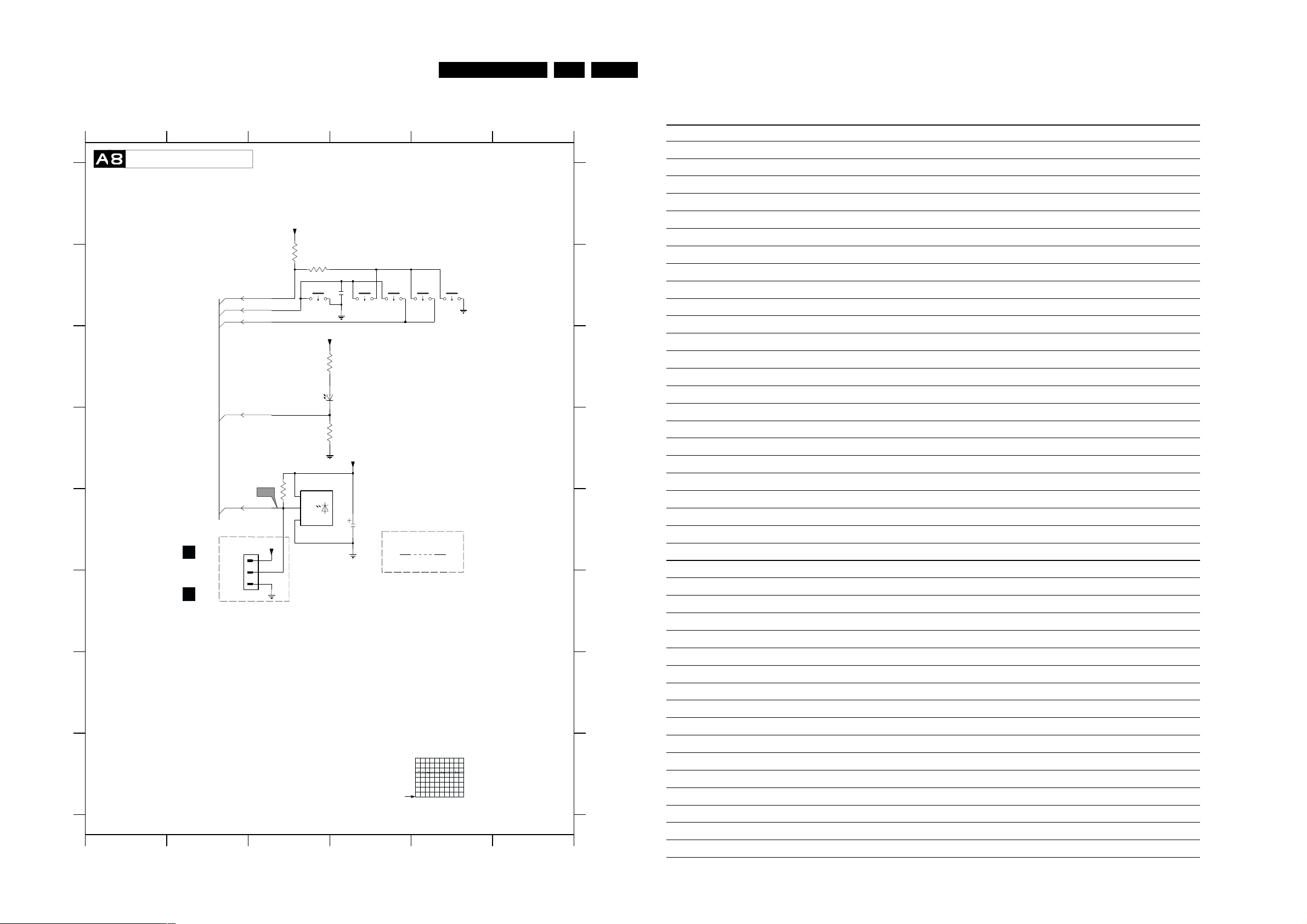
Schematics and PWB’s
Personal notes:
Front control
35L9H.2E 7.
A
A
B
B
C
C
D
D
123
123456
456
FRONT CONTROL
+5VD
8K2
3682
3683
100R
A7-14
A7-15
A7-16
A7-21
KeyBd1
KeyBd2
KeyBd3
LED
1684
USA
MAINS
+5VD
3680
6680
3681
2697
680R
LTL-307X
4K7
+5VD
1n
16821683 1681 1680
CH
CH
UP
DN
VOL
VOL
UP
FN
0259 E3
1680 B5
1681 B5
1682 B4
1683 B4
1684 B3
2680 E4
2697 B4
3680 C3
3681 D3
3682 B3
3683 B3
A
A
3684 E3
4600 E5
6680 C3
7680 D4
B
B
C
C
D
D
G
G
7680
3684
GP1U28QP
2
3K3
1
OUT
3
GND
VS
10u
2680
For Engg purpose only
46000259
E
E
C5
A7-28
E
E
TO
0259
For ITV only
I
SP/LS
OR
0259
IR
+5VD
1
2
3
J
F
F
H
H
(INTERFACE)
C5
G
G
F
F
H
H
1V / div DC
5µs / div
123456
12
34
56
CL 06532004_016.eps
110100

Schematics and PWB’s
Smart sound + Mono sound amplifier
36L9H.2E 7.
123456789101112
1701 D4
2702 E5
2703 E6
AM MONO DEMODULATOR
(for BG/I/LL’ Mono sets only)
2704 E7
2705 F7
2706 E7
2707 E9
2709 C7
2710 C7
A
3707 E8
3709 F7
3710 F8
3712 E9
3713 E9
4220 E8
7703 E8
7704 E9
7705 C5
B
+5VA
4u7
2710
100n
A5-39
A5-40
LLp|F1
LLp|F2
1
2
1701
2709
7705
TDA9830
4
CREF
4V4
16
2702
1V8
1V8
4u7
1
IFIN1
IFIN2
4
5
3
A1
13
GND
SUPPLY
BANDGAP
AGC
CONTROL
14
VP111VP2
AGC
DETECTOR
CAGC
3
2V4 1V2
2703
AMOUT
4u7
AMIN
6
A2
220n
2704
27K
3709
7
2V2
1552
NC
12
MUTE
SWITCH
EXTIN
9
2V2
0 dB
220n
2706
220n
2705
AFOUT
10
5V2
8
4220
2V2
3707
1V8
7703
47K
BC847B BC847B
3V1
4K7
3710
7704
3V7
2707
220n
3712
47K
FM|AM|ExtAudioMono
3713
150K
Sys2|AMFM_ExtSel
Sys1|AM
FM_AudioMono
FM|AM|Audio
ExtAudioMono
A7-27
A5-37
A7-26
A5-53
A5-45
A5-38
C
D
E
F
123456789
A1
10mV / div AC
5µs / div
CL 96532028_045.eps
10 11 12
G
H
070499

Schematics and PWB’s
Smart- and Mono sound Amplifier
37L9H.2E 7.
123456789101112
SMART SOUND + MONO SOUND AMPLIFIER
A
VlotAux8V
RES
3980
FM|AM|Ext_VC_AudioMono
A5-37
BassSw
A7-5
TrebleSw
A7-11
MainAudioL|Mono
A5-49
Buzzer
A7-2
Volume
A7-3
AudioSupply10V|14VA AudioSupply10V|14VA
4906
3V
3981
TO
0264
H1
(RADIO-SP/LS)
2955
470u
2V4
RES
SMART SOUND (MONO)
4907
3971
270R
7951
BC847B
3972
0264
2971
10u
1K
1
2
7952
BC847B
VlotAux8V
9953
2972
3975
3978
33n
5K6
12K
3973
470R
3974
6K8
3977
1K8
2950
10u
3983
RES
4908
1K8
3976
AudioSupply10V|14VA
100n
2973
3950
2976
RES
15K
3982
7955
BC847B
6953
BZX284-C3V3
27K
82n
2974
2975
3979
4905
* for ITV only
10n
220R
2953
220n
7956
BC857B
3953
2952
*
3K3
2956
*
A3
2951
10u
SpkrLpIn
AudioSupply10V|14VA
7953
*
3
2V4
5
0V7
Vref
NC
19
7954
*
NC1
7
2
4
Vref
19V
+
STABILIZER
TEMPERATURESTABILIZER
2954
*
2
VP
PROTECTION
AudioSupply10V|14VA
2957
1
+
-
TEMPERATURE
PROTECTION
0215A
RES
2959
0215B
1
2
RES
9V
8
9V
2958
764
A4
A5
*
5
8
SpkrLpOut
0215
A11-66
A11-67
Fishhooks for
Brazil only
SpkrLp
SpkrLn
To loudspeakers
OR
TO
0215
H1
(RADIO-SP/LS)
OR
TO
L3
I
( SP/LS)
B
C
D
E
0215 C10
0215A B11
0215B B11
0264 D4
2950 E5
2951 E7
2952 C7
2953 B6
2954 B8
2955 E3
2956 D7
2957 D9
2958 C10
2959 C10
2971 B4
2972 B5
2973 C5
2974 C6
2975 C6
2976 B6
3950 E5
3953 E7
3971 B3
3972 C3
3973 B5
3974 B5
3975 C5
3976 C5
3977 C5
3978 C5
3979 D6
3980 B3
3981 C3
3982 C5
3983 B5
4905 D6
4906 B3
4907 B4
4908 B5
6953 E6
7951 B3
7952 C4
7953 B7
7954 D7
7955 D5
7956 E6
9953 E5
9958 F3
AudioSupplyGnd
9958
MainSupplyGnd
36
F
Sound Control
Smart Sound
33nF
100nF -2973
82nF -2974
10nF -2975
470R -3973
6K8 Jumper3974
5K6 -3975
1K8
1K8 -3977
12K -3978
7952
7955 -BC847B
220R
BC847B -
-2972
-3976
-3979
2952
ON
OFFLHLH
*
BassSw
Sound Amplifier
1W
- 220nF2954
2n2 -2956
220nF -2957
- TDA7052B7953
TDA7056B -7954
TrebleSw
2W/3W/4WBasic Sound
2n2-
G
A3bA3d
1V / div DC
0.5ms / div
1V / div DC
0.2ms / div
CL 06532004_018.eps
110100
H
123456789101112

Schematics and PWB’s
Front cinch + Headphone
38L9H.2E 7.
1 2 3 4 5 6 7 8 9 10 11 12
FRONT CINCH + HEADPHONE
FRONT CINCH
4151
LEFT
5
5
6
6
YKC21-5599
YKC21-5599 7
4151,4153 for stereo set without front cinch
9122 for mono set without front cinch
4152 For Mono set Only
YKC21-5599
A6-57
SpkrLpIn
A10-66
SpkrRpIn
A11-70
0218-B
0218-A
0218-C
RIGHT
VIDEO IN
Ext1|2
3158
4
4
8
9
2
2
3
3
1
1
47K
3159
4152
47K
1153
1154
2174
4u7
4154
2177
4u7
4156
3156
120R
3157
120R
3151
1K
47K
3150
2171
330p
4153
3153
1K
47K
3152
1152
6161
330p
2172
BZX79-C6V8
HEADPHONE / SPEAKER
330p
2173
1150
2176
330p
1151
0249
3155
75R
Front|Ext1AudioL
Front|Ext1AudioR
Front|Ext1Video
Ext1Video
4
3
2
1
1
2
3
A5-47
A5-48
0230
TO 0260 OF
OR
TO 0229 OF
OR
NOT USED
FOR ITV
NOT USED
FOR ITV
Front I/O Configuration
SC1
SC1,Front
Cinch Mono
Mono
0218 - 0230
-0249 2171 - 2172 - 3150 - 3151 - 3152 - 3153 - 3155 - 4151 - Yes
4152 - 4153 - Yes
4155 - 4156 - -
-----
6161
Ye s
Ye s
SC1,SC2
Stereo
Ye s
-
SC1,Front
Cinch Stereo
A,B,C
Ye s
Ye s
330pF
330pF
47K
1K
47K
1K
-
-
-
-
-
Ye s
SC1,SC2,Side
AV Stereo
-B,C
-Ye s
-Ye s
--
-330pF
--
--
-47K
-1K
-
--
-
-
-Ye s
--
Headphone Configuration
Headphone
Stereo
0232
0232
YKB21-5099A1
6
5
4
2
3
7
8
9
4150
SpkrLpIn
SpkrLpOut
SpkrRpOut
SpkrRpIn
0217
1
2
3
1
2
3
4
5
0234
FOR
INDIA
ONLY
TO
0247
OF
OR
NOT USED
FOR ITV
NOT USED
FOR ITV
2173
330pF
2174 10uF 10uF
2176 330pF 330pF
2177 10uF 10uF
3156 270R 270R
3157 270R 270R
4154 - Yes
Headphone
Stereo
Ye sYes
-Ye s0234
330pF
C
D
0217 E6
0218-A C2
0218-B B2
0218-C D2
0230 C5
0232 E4
0234 F6
0249 B5
1150 E3
1151 F3
A
B
1152 D3
1153 B3
1154 C3
2171 B4
2172 C4
2173 E3
2174 E3
2176 F3
2177 F3
3150 B3
3151 A3
3152 C3
3153 B3
3155 D4
3156 E3
3157 F3
3158 E2
3159 E2
4150 F5
4151 A3
4152 B2
4153 B3
4154 F2
4156 D3
6161 D4
E
F
SpkrRpIn
SpkrLpIn
NOTE : 0191 use 242202604471 for INDIA only
for other regions use 242202604747
SpkrLpOut
SpkrRpOut
A11-73
A10-67
CL 06532004_019.eps
1 2 3 4 5 6 7 8 9 10 11 12
G
H
110100

Schematics and PWB’s
Rear I/O scart
39L9H.2E 7.
123456789101112
1
2
3
4
5
6
7
8
9
10
11
12
REAR I/O SCART (EUROPE)
2101
2103
75R
3109
75R
3112
6107
BZX284-C6V8
47K
TO 0605
A7
75R
3124
150R
330p
3104
150R
330p
100R
100R
3125
100R
3128
75R
3100
3108
3113
1109
3101
3105
220K
220K
1113
1107
1108
2109
7141
BC847B
+5VA
3142
1K
1101
1103
330p
5V
1V8
3120
1K
680R
3143
3102
330p
2102
3106
330p
2104
3110
3114
Ext1AudioL|Mono
47K
3121
2V4
1K
1K
1104
100R
75R
3115
100R
75R
3116
75R
Ext1AudioR
3111
3103
3107
4139
47K
47K
3122
10K
4141
4142
4133
3123
6K8
7140
BC847B
4140
0229
1
2
3
+5VA
3140
1K
4147
5V
1V8
2105
100u
680R
3141
0227
1
2
3
4
2V4
To 0253 of
or 0230 of
TO 0252 OF
OR 0249 OF
NOT USED
FOR ITV
4131
4132
7130
OR
7131
0V7 0V7
33R
TO
1227
3131
3130
J
33R
7132
4143
4148
0V7
3132
33R
7133
2106
10u
0V7
3133
33R
AudioOutL|Mono
Ext2AudioL|Mono
Ext1B
ScartPin8|SVHS
Ext1G
Ext1R
Ext1FB
VideoOut
AV_Mute
Ext1Video
Ext2Video
Ext2AudioL|Mono
ExtAudioMono
Ext2C
VideoOut
Ext2Video
Ext2Video|Y
Ext1Video
A5-44
A13-44
A5-42
A5-43
A5-41
A6-60
A7-12
A6-59
A6-58
A6-61
A12-13
A6-50
A13-50
A6-57
A13-57
A13-76
A13-41
A5-38
A6-55
A13-55
A13-50
A13-76
A6-54
A13-57
AudioOutR
A13-44
A13-55
A13-50
A13-76
Ext2C
VideoOut
Ext2Video|Y
SC1
SC1,Front
Mono
Cinch Mono
AA,B
0223
0227 0229 - 2107 - 330pF
2109
3102 1K 1K
3103 - 3106
3107 47K 47K
3118 - 1K
3119
3120 3121 - 47K
3124
3125 3128 - 75R
3135
3136 3140 Jumper Jumper
3142 - Jumper
3143 - 1K
4133 - -
4140
4141 - Yes
4147 Yes 6110
7141-9649 Yes -
Ye s
-
- 330pF
1K 1K
Jumper
- 47K
-
- 75R
-
-
-
Ye s -
-
- BZX284
-
SC1,SC2
Stereo
Ye s
1K
100R
4K7
15K
Ye s-4139
C6V8
BC847B
for ITV only
0214
1
2
3
0216
1
2
3
4
SC1,Front
Cinch Stereo
Jumper
Ye s
Ye s
47K
47K
Ye s
A
-
-
1K
1K
-
-
-
-
-
-
-
-
-
-
-
-
-
-
-
-
-
--Yes
TO
0214
J
(SMART CARD
INTERFACE)
TO
0216
J
(SMART CARD
INTERFACE)
SC1,SC2,Side
AV Stereo
A,BA
Ye s
Ye sYe s
330pF330pF
1KJumper
47K-
1K
47K-
Jumper-
-
Jumper-
--
75R-
100R-
75R4K7-
15K
JumperJumper
Jumper-
1K
-Yes
--
-
Ye sYe s
-Yes
BZX284
C6V8
BC847B
A
A
B
B
C
C
D
D
E
E
F
F
G
G
H
H
Audio R O/P
Audio R I/P
Audio L O/P
Audio L I/P
RGB B I/P
RF/Video1 Switching
RGB G I/P
RGB R I/P
RGB FB I/P
CVBS O/P
Video 1 I/P
Audio R O/P
Audio R I/P
Audio L O/P
Audio L I/P
RF/Video2 Switching
C I/P
CVBS O/P
Video 2/Y I/P
0223-A
SCART 1
0223-B
SCART 2
1A
2A
3A
4A
5A
6A
7A
8A
9A
10A
11A
12A
13A
14A
15A
16A
17A
18A
19A
20A
21A
1B
2B
3B
4B
5B
6B
7B
8B
9B
10B
11B
12B
13B
14B
15B
16B
17B
18B
19B
20B
21B
1111
2107
1119
1110
1102
1105
1106
1132
3118
1K
330p
3136
15K
3135
1115
6110
1117
BZX284-C6V8
5100
1U
5101
1U
3119
0105
1
4K7
1118
0105 E3
0214 A11
0216 B11
0223-A A2
0223-B E2
0227 E6
0229 H6
1101 A4
1102 B3
1103 B4
1104 C5
1105 C3
1106 C3
1107 C4
1108 D4
1109 D3
1110 A3
1111 E2
1113 F3
1115 G2
1117 H2
1118 G3
1119 F2
1132 D3
2101 A3
2102 A4
2103 B3
2104 B4
2105 C6
2106 B8
2107 E2
2109 F3
3100 A3
3101 A4
3102 A5
3103 A5
3104 B3
3105 B4
3106 B5
3107 B5
3108 B3
3109 C3
3110 C4
3111 C5
3112 C3
3113 C3
3114 D4
3115 C5
3116 D5
3118 E3
3119 E3
3120 E4
3121 F4
3122 B5
3123 C6
3124 G3
3125 G3
3128 G3
3130 D7
3131 D7
3132 D8
3133 D8
3135 F3
3136 F3
3140 D6
3141 D6
3142 F4
3143 G4
4131 A7
4132 A7
4133 F6
4139 H5
4140 F6
4141 H5
4142 H5
4143 E8
4147 F6
4148 E8
5100 A3
5101 B3
6107 D3
6110 H3
7130 D7
7131 D7
7132 D8
7133 D8
7140 D6
7141 G4
1
1234
2
3
4
CL 06532004_020.eps
5
6
756789101112
9
10
11
130100
128

Schematics and PWB’s
CRT
40L9H.2E 7.
123456789101112
2
3
4
5
6
7
8
91
10
11
12
CRT PANEL
160V 160V
A
A
B
B
C
C
D
D
E
E
F
F
TO 0243
OF
0245
6
5
4
3
2
1
OLDGND
BLKCURINFO
BLUE
GREEN
RED
V13
V11
160V
33K
3334
129V
7331
2V4
BF422
1V9
2331
220p
1K
3332
3331
OLDGND
3321
OLDGND
3311
OLDGND
470R
33R
160V
V12
129V
7321
2V4 1V2
BF422
1V9
2323
1K
3322
330R
3323 3333
129V
7311
BF422
1V9
2313
1K
3312
470R
3313
220p
33R
220p
33R
3324
160V
3314
33K
33K
9300
6342
1N4148
129V
129V
129V
3336
190V
7332
BF422
140V
7333
BF423
1V2
160V
3326
190V
7322
BF422
140V
7323
BF423
160V
3316
190V
7312
BF422
140V
7313
BF423
1V22V4
OLDGND
220R
220R
220R
6341
BAV21
6321
6311
BAV21
6331
BAV21
BAV21
3347
0165
GND
1K5
3337
V16
V14
3317
1K5
3327
1K5
1300
1
3
4
5
6
7
8
9
Blue
Green
Blue
Green
Red
Red
V15
0254
1
G
4
5
6
7
8
100R
NEWGND
9
10
11
12
1K5
1K5
3341
3348
NEWGND
3349
3350
100R
NEWGND
1K
2341
680p
Ground
Heater
Heater
CRT
9 Pin 12 Pin
GND
Green
Pin 7 Pin 8
Red
Heater Pin 5 Pin 9
Heater Pin 4 Pin 10
Blue Pin 3 Pin 11
VG1 VG2
Pin 1 & 12Pin 1
Pin 5Pin 6VG1
Pin 6Pin 9
Pin 7Pin 8VG2
VG2
FROM MAIN CHASSIS
FOCUS
LOT OF
EHT
VG2 F10
0165 B8
0244 G3
0245 C2
0254 D8
1300 B8
2313 F4
2323 D4
2331 B4
2341 F6
2342 H3
2343 H4
3311 F3
3312 F4
3313 F4
3314 E4
3316 D5
3317 C6
3321 D3
3322 D4
3323 E4
3324 C4
3326 C5
3327 C6
3331 C3
3332 C4
3333 C4
3334 B4
3336 A5
3337 B7
3341 E6
3347 F5
3348 E6
3349 F7
3350 F7
5341 G3
5342 H3
6311 E5
6321 C5
6331 B5
6341 A5
6342 G4
6343 G6
7311 F4
7312 E5
7313 E5
7321 D4
7322 C5
7323 D5
7331 B4
7332 B5
7333 B5
9300 F4
G
070499
G
H
H
160V
0244
TO
0220 OF
123456789101112
1
3
2
1
37
2342
NEWGND
5341
47n
5342
22u
22u
2343
OLDGND
FILEMENT
15n
4
5
6343
OLDGND
BZX284-C8V2
6
82 9
V14 V15 V16
50V / div DC
20µs / div
10
50V / div DC
10µs / div
11
50V / div DC
10µs / div
CL 96532028_049.eps
12

Schematics and PWB’s
41L9H.2E 7.
CRT panel (component side)
CRT panel (copper side)
External power supply
EPS (external power supply)
TO
(Power supply)
MAINS
HOT GROUND
0211
A1
live
neutral
ZD1
P6KE150
D1
UF4005G
IC1
TOP222P OR
MIP222P
1
2
3
4CONTROL
L6
HF50B
0211
live
1
neutral
2
0213
1
2
8
7
6 SOURCE
DRAIN5
400V
C38
RES
F1
T1A/250V
1
2
C4
RES
T1
C2
470P
P11
L2
22mH
B
C
A
3
4
R12
22R
R23
43R
C20
100n
C12
1n
CR2
SB3100
CR1
SB540
51DQ04
1N4148
C24
FF
+
L7
HF70B
R16
2k0
P10
300V
C5
33u
0228
+12V
P13
5V
C23
470u
R15
2k05
C36
100n
+
R24
1k0
L8
HF70B
+5V
TO
3
0228
2
J
(Interface)
1
J1
TO GROUND
1
MAIN CHASSIS
CL 96532141_026.eps
071299
+
C11
220u
+
C7
470u
C21
100n
6V
R11
22R
C6
47u
L1
22mH
IC4
KA78R12 AN7812
32
1
4V
IC3
UTC431/
AN431
-
12V
+
5V
C29
100n
C35
330u
R13
22R
DI106
P12
L5
12u
IC2
PS2561-V
TLP-721
R14
2k0
2V5
C1
0u1
1n
19V
5V
D2
13V5

Schematics and PWB’s
42L9H.2E 7.
Clock display panel
1
2
3
4
5
6
7
CLOCK DISPLAY
A A
2V8
2V11
7955
3954
DP1
4
3
2
1
+5v+5v +5v+5v
BC817C
100R
TO 0247
(RADIO)
OR
TO
0237
(INTERFACE)
J
7
2V5
BC817C
8
DP
G
F
6
1
7953
3952
100R
7951
SAA1064
+5v
6951
6952
ALARM
7957
3
PC
10
A
9
B
D
C
5
4E2
7
5137910816431220 18 16215 172319 21242211 14
P6
P2P1P3
MX2
MESSAGE
8
B656
2V8
6
DP
1
G
F
P7
P8
P14
P12
P10
P9
10
9
7
P11
A
B
C
P13
3
PC
D
5
4E2
P15
P16
LED-DRIVER WITH I2C-BUS INTERFACE
VCC P4
ADR P5
VEE
5V
2951
2953
100u
100nF
3
4
CEXT
2V9
2952
2n7
B653
SDA
4V8
SCL
7958
8
DP
G
F
B652
4V6
2V8
BC817C
7952
B B
3951
C C
D D
100R
B655
2V11
7956
10
9
7
3
PC
A
B
D
C
5
4E2
E E
1
2
5
6
1
3953
MX1
100R
3956
BC817C
7954
100R
+5v
10
3955
100R
7959
3
8
PC
6
A
DP
1
9
B
G
D
C
F
5
4E2
7
B651
B650
+5V
SCL
SDA
6
2951 E 3
2952 E 4
2953 E 4
3951 B 1
3952 B 3
3953 B 5
3954 B 7
3955 E 6
3956 E 5
6951 B 4
6952 B 4
7951 D 3
7952 B 1
7953 B 3
7954 B 5
7955 B 7
7956 B 2
7957 B 3
7958 B 5
7959 B 6
B650 E 6
B651 E 6
B652 E 5
B653 E 5
B655 D 1
B656 B 4
DP1 D 7
Radio panel
1
EC
9942
LS
J1
J2
SP
1
6
11
B
EC
B
EC
3940
B
EC
3941
9940
AK
KA
KA
KA
AK
14
13
FM TUNER
1901
9941
1
2
11
12
AK
9941
B
8
11
1
717
C
B
E
9910
16 9
1
OG I
8
9912
1
9913
10 9
3900
9922
1
48
AK
1
CL0532004_025.pdf
270100
0237
0255
1
0247
1
0256 0264
4921
3908
2930
E
B
3934
7930
3930
C
3931
4930
9
8
12
16
1
111
2
3908
9
16
4920
8
1
3907
3902
3921
3920
3912
2906
2907
3915
3911
3909
3905
CL 06532004_023.pdf
170100

Schematics and PWB’s
Radio panel
43L9H.2E 7.
1
2
3
4
5
6
7
8
9
10
11
12
13
14
RADIO - SP/LS - Vbat
2940
2942
100n
10K
3945
1920
MP25
7920
LM7805
IN
GND
G
B027
2
9942
3941
res
3940
res
res
2941
SP/LS
3944
0V
10K
3946
100
3947
100
6950
0V
res
2952
3948
0V
res
7950
res
Vbatt
B013
OUT
2n2
3952
res
res
+5E
2920
9943
9944
+5E
10K
3943
7940
BC547B
B006
B008
res
7951
res
res
3951
B012
1V6
7925
BF422
10uF
5940
res
5941
res
7952
+5E
res
3949
0V
3K3
3928
3
B025
SpkrLp
SpkrLn
B026
B007
5V
Dout
Din
POR-CLK
B009
0V
B010
res
3950
1V8
+5E
Vbat SUPPLY
res
3932
3930
100K
3933
SMD
5W
0215
1
2
res
5950
res
TO 0215
(AUDIO)
STANDBY
0238
1
2
3
4
5
3
2
1
0259
res
+5E
4K7
3931
SMD
2930
470p
4
TO 0238
(CONTROL)
N.C.
5V
10K
3934
7930
BC847B
0V7
SMD
ONLY FOR RADIO VERSION
+5E
3910
47K
3911
SMD
2908
2906
2907
3926
3K3
1uF
470p
SMD
470p
SMD
3914
5
6
3
2
33K
3927
3K3
+5E
B029
11V8
6
SMD
3912
3913
SMD
5
47K
33K
2V5 2V5
3925
3K3
22
7903
8
TDA1308
7
4
3915
220K
SMD
7903
B
TDA1308
1
3909
220K
SMD
1901
1
11
9
7
8 10
6925
BZX79C12
AERIAL
4930
res
2909
A
2V5
2V5
OM5610 FM TUNER
B016
47uF
3904
3905
SMD
2
12
5
6
3
4
1413
7
B017
1K
B018
1K
+5E
7904
PCF8574A
5V
STEREO
1V2
DATA
4V
WR-EN
4V8
CLK
B028
0V7
SEL-RADIO
2901
22uF
2904
22uF
13
NC
4
5
6
7
9
10
11
12
B015B014
RADIO
4920
SMD
3907
2V2
3901
1K
6901
P0
P1
P2
P3
P4
P5
P6
P7
VSS
8
2911
2902
10uF
SMD
15K
SMD
res
3921
15K
3902
2903
SMD
3920
10uF
BZX79C2V4
I/O EXPANDER FOR I2C BUS
READ IIC CONTROL
WRITE
8
9
res
res
3917
2V2
1V2
0V2
1V2
0V7
1K
IIC
16
1
2
3
5
13
12
SMD
+5E
678
H
L
1011
VDD
A0
A1
A2
SCL
SDA
10
9
5V
15
4
14
16
5V
1
2
3
14
5V
15
4V5
4V8
1V2
7901
HEF4053B
3916
220
22uF
2910
10K
3919
3918
+5E +5E
11
+5E
3908
2905
B023
B024
10K
4K7
10uF
+5E
4921
res
3906
6K8
9922
res
3922
res
SMD
SEL-RADIO
12
B019
2921
res
+5E
AUDIO-TV
AUDIO-OUT
B020
B021
B022
0247
4
3
0264
1
2
1
2
0256 res
TO DP1
SCL2
2
SDA2
(CLOCK)
1
4
3
SCL2
TO 0237
2
SDA2
1
(CONTROL)
0237
TO 0239 AND 0240
1
1
23456
7
0239
ONLY FOR MECHANICAL CLAMPING
23456
0240
CL 06532004_011.eps
13
TO 0264
(AUDIO)
7
130100
14
A A
1940
HEADPHONE
CONNECTOR
J1
J2
B B
+5E
C C
1950
P3
P2
D D
B001
B002
100
3942
0V
6945
BZX79C5V6
B003
P4
E E
P1
SMART LOADER CONNRCTOR
RJ11
TO 0255
1-2
AND
TO 0241
3-4-5
P5
P6
F F
G G
H H
B004
B005
0255
1
2
3
4
5
4V5
6946
4V3
6947
0V
6948
95V
BZX79C5V6
BZX79C5V6
res
B011
(SUPPLY)
5V
I I
1
1 F 6
2 F 6
3 G 6
4 G 6
5 F 6
6 F 6
7 G 6
8 G 6
9 F 6
10 G 6
11 F 6
12 F 6
13 G 6
14 G 6
0215 A 4
0237 H14
0238 D 4
0239 I12
0239 I12
0239 I13
0239 I13
0239 I13
0239 I13
0239 I13
0240 I13
0240 I14
0240 I14
0240 I14
0240 I14
0240 I14
0240 I14
0247 H13
0255 H 1
0256 C13
0259 F 4
0264 B14
1901 H 6
1920 H 2
1940 A 1
2901 C 8
2902 B 9
2903 E 9
2904 C 8
2905 E11
2906 D 5
2907 D 5
2908 C 5
2909 B 7
2910 F11
2911 B 9
2920 I 2
2921 B13
2930 I 4
2940 B 2
2941 B 3
2942 C 2
2952 F 3
3901 D 8
3902 D 9
3904 C 7
3905 C 7
3906 C12
3907 D 8
3908 E11
3909 D 6
3910 B 6
3911 B 5
3912 C 5
3913 E 5
3914 E 5
3915 C 6
3916 F11
3917 E 9
3918 H11
3919 H11
3920 D 9
3921 D 9
3922 C12
3925 G 3
3926 G 4
3927 G 4
3928 I 3
3930 I 3
3931 I 4
3932 I 3
3933 I 4
3934 G 5
3940 A 3
3941 A 3
3942 C 1
3943 C 3
3944 D 2
3945 D 2
3946 D 2
3947 E 2
3948 F 2
3949 F 3
3950 F 4
3951 G 3
3952 E 3
4920 C 8
4921 A12
4930 I 6
5940 A 3
5941 B 3
5950 G 4
6901 E 8
6925 H 4
6945 D 1
6946 E 1
6947 F 1
6948 G 1
6950 E 2
7901 C11
7903 B 6
7903 D 6
7904 F 7
7920 H 1
7925 I 3
7930 I 5
7940 D 3
7950 G 2
7951 F 3
7952 E 3
9922 C12
9942 A 3
9943 A 3
9944 B 3
B001 C 1
B002 D 1
B003 D 1
B004 E 1
B005 F 1
B006 D 4
B007 D 4
B008 E 4
B009 E 4
B010 E 4
B011 H 1
B012 G 3
B013 H 2
B014 I 5
B015 I 8
B016 G 5
B017 C 7
B018 C 7
B019 B13
B020 C13
B021 C13
B022 C13
B023 H12
B024 H12
B025 A 4
B026 B 4
B027 I 1
B028 G 7
B029 G 5
J1 A 2
J2 B 2
P1 E 1
P2 D 1
P3 C 1
P4 D 1
P5 F 1
P6 F 1

Schematics and PWB’s
CL96532159_032.pdf
060100
Personal notes:
44L9H.2E 7.
Interface panel

Schematics and PWB’s
45L9H.2E 7.
Smart plug / loudspeaker
I
SMART PLUG/LOUDSPEAKER SP/LS
+5V
SMART PLUG LOADER
CONNECTOR
U1
Clock
Data-in
+5V
Data-out
Ground
IR-data
RJI1
1
2
3
4
5
6
R6
100R
C3
100n
0V
D5
BZX79-C3V6
4V6
5V
D1
BZX79-C5V6
R7
100R
D0
BZX79-C5V5
0V
BC547B
Q3
R3
10K
D2
BZX79-C5V6
R2
10K
BC557B
Q2
R4
100R
R5
100R
+5V
R6
47K
R13
47K
+5V
Q1
BC547B
R6
10K
Smart plug / loudspeaker panel
TO/FROM
0238
1
2
3
4
5
0259
1
2
3
0238
A7
CONTROL
TO/FROM
1238
(SMART CARD
INTERFACE)
To/from
0259
(SMART CARD
INTERFACE)
To/from
0259
Stdby
Data-out
Data-in
CLK
Gnd
+5V
R11
5V
47K
+5V
IR-Data
DCM Disable
A8
CONTROL
0V
OR
J
I
or
FOR
NON SYSTEM
FOR
SYSTEM
FOR
SYSTEM
FOR NON
SYSTEM
BATHROOM SPEAKER
CONNECTION
U3
1
4
2
BZX79-C20
D4
0.1V 0V 0V
1N4148
D9
BZX79-C20
D8
R10
10R
C2
100n
R9
10R
JP3
R12
47K
Q4
BC547B
L3
1
Spk +
2
Spk -
J7
1
Not used
2
TO
0215
A10
(SOUND
AMPLIFIER)
CL 06532004_021.eps
110100

Schematics and PWB’s
Smart card interface
46L9H.2E 7.
12345678
SMART CARD INTERFACE
J J
330R
+5Veps
56u
1u
3704
4717
3720
2
68K
1700
250mA
MP
3721
75R
1K
7710
DS1813
RESET
PULS
FORMER
6710
3716
47K
1
3
0V
BAS216
2704
DCM DISABLE
+5Veps
3717
22K
3705
1u
10K
5V4
I
SP/LS
A8
FRONT
CONTROL
+5Veps
7702
BC847B
3708
2701
5K6
3706
100n
0259
1259
22K
1
2
3
1
2
3
3707
4716
IR DATA
0V7
22K
IR DATA
0V
7703
BC847B
+5Vchas
6700
BZX284-C8V2
3711
4K7
+5Veps
4V8
AUDIO OUT
MONO +
AUDIO OUT
BC847B
MONO -
3713
4K7
BC857B
7705
1V2
0V
7707
+5Veps
1215
1
2
3714
4V9
0V
4K7
3712
10K
BC857B
7704
3722
1K8
+5Veps
0V
3715
10K
FROM 0263
A13
I/O SCART
0214
AUDIO RIGHT
1
2
AUDIO LEFT
3
SMART CARD
CONNECTOR
1800
1
2
3
4
5
6
7
8
9
10
11
12
13
14
15
16
17
18
19
20
GND-E GND
GND-D
21
22
23
24
25
26
27
28
29
30
31
32
A
B
C
D
E
F
F
EPS
I
SP/LS
A7
CONTROL
A7
CONTROL
A7
CONTROL
A13
I/O SCART
G1
CLOCK
DISPLAY
A13
I/O SCART
A1
SUPPLY
0228
1238
0238
0236
0219
0216
0237
1227
0241
1
1
2
3
1
2
3
4
5
1
2
3
4
5
1
2
3
4
1
2
3
4
5
1
2
3
4
1
2
3
4
1
2
3
4
1
2
3
4
5
+12Veps
GND-E
SDA2
+5Veps
GND-C
GND-D
+5Veps
TV DATA
DCM DATA
CLOCK
TV DATA
DCM DATA
CLOCK
RESET
ANALOG RED
ANALOG GREEN
ANALOG BLUE
FAST BLANKING
"C" IN
SCL2
AUDIO IN RIGHT
AUDIO IN LEFT
Vaux
VD
HD
6712
BYD33D
+5Vchas
4V6
6701
6707
3703
GND-E
+5Vchas
4V6
4V6
6702
BZX284-C8V2
6706
BZX284-C8V2
75R
3702
6711
BYD33D
2703
1u
+5Veps
47K
10K
3701
3700
6704
SDA2
SCL2
A7
4V6
7701
BC847B
+12Veps
BZX284-C8V2
3718
2V
100R
0V
3719
12V
7706
BC847B
1V4
GND-E
6703
BZX284-C8V2
6705
BZX284-C8V2
VIDEO OUT
CVBS/Y IN
75R
1237
1
2
3
4
7700
BC847B
BZX284-C8V2
0V
0V
0V
0V
BZX284-C8V2
CONTROL
3723
5705
8V
2702
2700
47n
33R
+12Veps
4715
2345678
GND POWER
GND IIC
TV CLOCK
DCM DATA
CVBS_IN
2
2
CVBS_OUT
CVBS_OUT
AUDIO OUT MONO+
(SPEAKER)
AUDIO OUT MONO(SPEAKER)
AUDIO RIGHT OUT
AUDIO LEFT OUT
CL 065320004_022.eps
110100
A
B
C
D
E
F
0214 E7
0216 D1
0219 C1
0228 A1
0236 C1
0237 E1
0238 B1
0241 F1
0259 A4
1215 E6
1227 E1
1237 E2
1238 A1
1259 B4
1700 A3
1800 B8
2700 F3
2703 A3
3700 B2
3701 B2
3702 E2
3703 E2
3704 F3
3705 F3
3711 C5
3712 C6
3713 C6
3714 C6
3715 C7
3716 B3
3717 B3
3718 D2
3719 D3
3721 D3
3722 D6
3723 F3
4715 F2
4717 B3
6701 C2
6702 C2
6703 C2
6704 D2
6705 E3
6706 D2
6707 D2
6710 F3
6711 F2
6712 F1
7700 B2
7701 B3
7704 C6
7706 D3
7707 D6
7710 F3
 Loading...