

Philips 160E1SB/97, 160E1SB/94, 160E1SB/00, 160E1SB/78, 160E1SB/93 Service Manual
...
15.6Ǝ LCD Color Monitor Chassis: Meridian 1
Service
Service
Service
Description
Page Description Page
Page
SAFETY NOTICE
ANY PERSON A TTEMPTING TO SERVICE THIS CHASSIS MUST F A MILIARIZE HIMSELF WITH THE
CHASSIS AND BE AWARE OF THE NECESSARY SAFETY PRECAUTIONS TO BE USED WHEN
SERVICING ELECTRONIC EQUIPMENT CONTAINING HIGH VOLTAGES.
CAUTION: USE A SEPARATE ISOLATION TRANSFOMER FOR THIS UNIT WHEN SERVICING
Table of Contents........................................………….1
Revision List................................................…………….2
Important Safety Notice………….................................3
1. Monitor Specifications….............................................4
2. LCD Monitor Description….........................................5
3. Operation instructions….............................................6
3.1General Instructions……………………………….…...6
3.2 Control buttons…………..……………………….……6
3.3 OSD Menu…………………....................................8
4. Input/Output Specification.........................………….10
4.1 Input Signal Connector...........................…………..10
4.2 Factory Preset Display Modes................................10
4.3 Pixel Defect Policy……………………………………11
4.4 Failure Mode of Panel …………………………….…14
5. Block Diagram……………………………................15
5.1 Software Flow Chart............................………….....15
5.2 Electrical Block Diagram.....................……….........17
6. Schematic Diagram…...............................................19
6.1 Main Board………………………………………………19
6.2 Power Board………….………………..…………………23
6.3 Key Board…….………………………..…………………25
7. PCB Layout………………………………………………...26
7.1 Main Board………………………………………………..26
7.2 Power Board………………………………………...……28
7.3 Key Board………...………………………………………30
8. Wiring Diagram……………………………………….…..31
9. Scalar Board Overview………………………………....32
10. Mechanical Instructions………………………………....33
11. Repair Flow Chart…….…….……………………………36
12. ISP Instructions...….................................................... .42
13. DDC Instructions…................................................. .....45
14. White Balance, Luminance Adjustment……................51
15. Monitor Exploded View….............................................53
16. Recommended & Spare Parts List...……...................54
17. Different Parts List………………………………………67
18. General Product Spe cification………………….……….71
312278518370
GB
REFER TO BACK COVER FOR IMPORTANT SAFETY GUIDELINES
Copyright 2008 Philips Consumer Lifestyle Subject to modification ƻK Jan. 12, 2009
160E1SB/75
160E1SB/70
160E1SB/71
160E1SB1/94
160E1SB1/97
160E1SB/55
160E1SB/93
160E1SB/97
160E1SB/00
160E1SB/05
160E1SB/62
160E1SB/94
160E1SB/78

!
!
Meridian 1
2
Revision List
Version Release Date Revision History
A00 Jan.12,2009 Initial release, Draft Versio n
A01 Jan.20,2009 Add CTV Model 160E1SB/94
A02 May.13,2009 Add CTV Model 160E1SB/78
A03 Oct. 24,2009 Add TPV OWN panel for 160E1SB/62, 160E1SB/94 and 160E1SB/97
A04 Dec.08,2009
Add CTV Model 160E1SB/75
Add TPV OWN panel for 160E1SB/00
Add AUO panel for 160E1SB/00, 160E1SB/62, 160E1SB/93, 160E1SB/94 and
160E1SB/97
A05 Jun.26,2010 Update AUO panel BOM for 160E1SB/93
A06 Jul.30,2010 Add CTV Model 160E1SB/70, 160E1SB/71, 160E1SB1/94 and 160E1SB1/97
A07 Oct.28,2010 Add TPV OWN panel for 160E1SB/70
A08 Jan.19,2011 Add IVO panel for 160E1SB/93
A09 Apr.19,2011 Add AUO pan el for 160E1SB/94
A10 Jul.07,2011 Add CTN mode 160E1SB/55
A11
Jul.13,2011 Update BOM for 160E1SB/55

3
Meridian 1
Important Safety Notice
Proper service and repair is important to the safe, reliable operation of all Philips Company Equipment. The servi ce
procedures recommended by Philips and described in this service manual are effective methods of performing
service operations. Some of these service operations require the use of tools specially designed for the purpose.
The special tools should be used when and as recommende d.
It is important to note that this manual contains various CAUTIONS and NOTICES which should be carefully read
in order to minimize the risk of personal injury to service personnel. The possibility exists that improper service
methods may damage the equipment. It is also important to understand that these CAUTIONS and NOTICE S ARE
NOT EXHAUSTIVE. Philips could not possibly know , evaluate and advise the service trade of all conceivable ways
in which service might be done or of the possible hazardous consequences of each way. Consequently, Philips has
not undertaken any such broad evaluation. Accordingly, a customer who uses a service procedure or tool which is
not recommended by Philips must first satisfy himself thoroughly that neither his safety nor the safe operation of
the equipment will be jeopardized by the service method selected.
Hereafter throughout this manual, Philips Company will be referred to as Philips.
WARNING
Use of substitute replacement parts, which do not have the same, specified safety characteristics, may create
shock, fire, or other hazards.
Under no circumstances should the original design be modified or altered without written permission from Philips.
Philips assumes no liability, express or implied, arising out of any unauthorized modification of design.
Customer assumes all liability.
FOR PRODUCTS CONTAINING LASER:
DANGER- There is invisible laser radiation when open. AVOID DIRECT EXPOSURE TO BEAM.
CAUTION-Use of controls or adjustments or performance of procedures other than those specified herein may
result in hazardous radiation exposure.
CAUTION -The use of optical instruments with this product will increase eye hazard.
TO ENSURE THE CONTINUED RELIABILITY OF THIS PRODUCT, USE ONLY ORIGINAL MANUFACTURER'S
REPLACEMENT PARTS, WHICH ARE LISTED WITH THEIR PART NUMBERS IN THE PARTS LIST SECTION
OF THIS SERVICE MANUAL.
Take care during handling the LCD module with backlight unit
-Must mount the module using mounting holes arranged in four corners.
-Do not press on the panel, edge of the frame strongly or electric shock as this will result in damage to the screen.
-Do not scratch or press on the panel with any sharp objects, such as pen cil or pen as this ma y result in damage to
the panel.
-Protect the module from the ESD as it may damage the electronic circuit (C-MOS).
-Make certain that treatment person’s body is ground ed through wristband.
-Do not leave the module in high temperature and in areas of high humidity for a long time.
-Avoid contact with water as it may a short circuit within the module.
-If the surface of panel becomes dirty, please wipe it off with a soft material. (Cleaning with a dirty or rough cloth
may damage the panel.)

!
!
Meridian 1
4
1. Monitor Specifications
1.1 Technical specifications
LCD Panel
• Type
TFT LCD
• Screen size 15.6Ǝ Visual
• Pixel pitch 0.252 x 0.252mm
• LCD Panel type
1366 x 768 pixels
R.G.B vertical stripe
Anti-glare polarizer, hard coated
• Effective viewing area 3 4.2 x 193.5 mm
Display Colors 16.7M
Scanning
• Vertical refresh rate 56 Hz – 76 Hz
• Horizontal Frequency 30 kHz - 60 kHz
Video
• Video dot rate 140 MHz
• Input impedance
- Video 75 OHM
- Sync 2.2K OHM
• Input signal levels 0.7Vpp
• Sync input signal
Separate Sync
Composite Sync
Sync On Green
• Sync polarities Positive and Negative
* This data is subject to change without notice.
5
Meridian 1
1.2 Physical specifications
• Tilt - 5°~ 20°
• Power supply 100~ 240 VAC, 50/60Hz
• Power consumption <35W * (typ.)
• Temperature
0 to 40 (operating)ćć
-20 to 60 (storage)ćć
• Relative humidity 20% to 80%
• System MTBF 50K hours (CCFL 50K hours)
• Cabinet color 160E1SB: black
2. LCD Monitor Description
The LCD monitor will contain a main board, a power board an d a key board which house th e flat panel control logic,
brightness control logic and DDC.
The power board will provide AC to DC Inverter voltage to drive the backlight of panel and the main board chips
each voltage.
Monitor Block Diagram
AC-IN
100V-240V
Power board
(Include: Adapter, Inverter)
Flat Panel and
CCFL backlight
Main Board
RS232 Connector
For white balance
adjustment in factory
mode
CCFL Drive.
Video signal, DDC
Key Board
HOST Computer
!
!
Meridian 1
6
3. Operating Instructions
3.1 General Instructions
Press the power button to turn the monitor on or off. The other cont rol knobs are located at front panel of the
monitor (see figure). By changing these setting, the picture can be adjusted to your personal preference.
γ The power cord should be connected.
γ Press the power button to turn on the monitor. The power indicator will light up.
3.2 Control Buttons
Front View
1
To switch monitor’s power on and off
2
MENU/OK
To access OSD menu/Confirm
3
/
To adjust brightness of the display
4
/
Auto picture control switching in wide and 4:3 formal
5
AUTO/
Auto adjust the horizontal position, vertical position, phase and clock settings
Return to previous OSD level

7
Meridian 1
Rear View
1 Kensington anti-thief lock
2 AC power input
3 VGA input
!
!
Meridian 1
8
3.3 OSD Menu
Description of the On Screen Display
This is a feature in all Philips LCD monitors. It allows an end user to adjust screen performance of the monitors
directly through an on-screen instruction window. The user interface provides user-friendliness and ease-of-use
when operating the monitor .
Basic and simple instruction on the control keys
When you press the MENU/OK button on the front control of your monitor, the On-Screen-Display (OSD) main
controls window will pop up and you can then start making adjustments to your monitor’s various features. Use the
Ÿź keys to make your adjustments.
9
Meridian 1
The OSD tree
Below is an overall view of the structure of the On-Screen Display. You can use this as a reference when you want
to work your way around the different adjustments later on.
!
!
Meridian 1
10
4. Input/ Output Specification
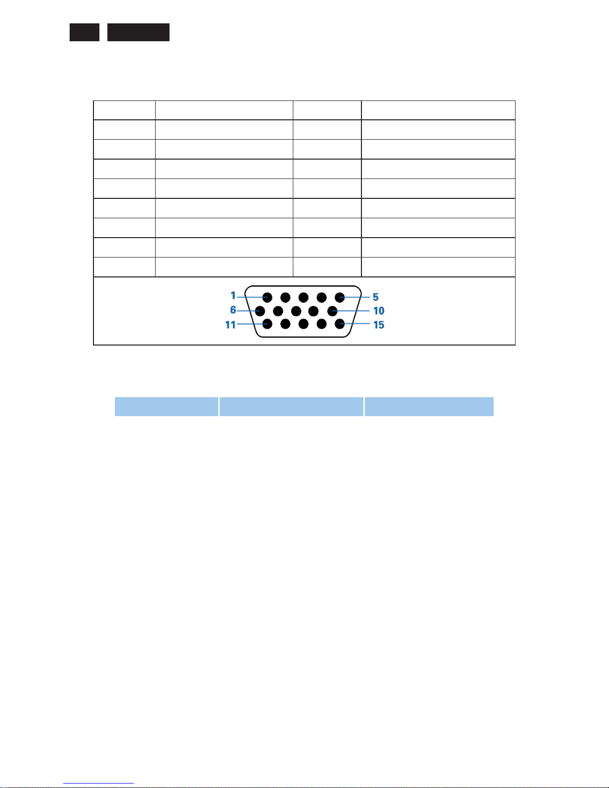
4.1 Input Signal Connector
Analog connectors
Pin No. Description Pin No. Description
1 Red video input 9 DDC +5V
2 Green video i nput (SOG) 10 Logic ground
3 Blue video input 1 1 Ground
4 Sense (GND) 12 Serial data line (SDA)
5 Cable dete ct (GND) 13 H.Sync/ H +V.Sync
6 Red video ground 14 V.Sync
7 Green video ground 15 Data clock line (SCL)
8 Blue video ground
4.2 Factory Preset Modes
H. freq (KHz) Resolution V. freq (Hz)
31.47 720*400 70.09
31.47 640*480 59.94
37.50 640*480 75.00
37.88 800*600 60.32
46.88 800*600 75.00
48.36 1024*768 60.00
60.02 1024*768 75.03
47.74 1366*768 59.79
11
Meridian 1
4.3 Pixel Defect Policy
Philips strives to deliver the highest quality products. We use some of the industry’s most advanced manufacturing
process and practice stringent quality control. However, pixel or sub pixel defects on the TFT LCD panels used in
flat panel monitors are sometimes unavoidable. No manufacturer can guarantee that panels will be free from pixel
defects, but Philips guarantees that any monitor with an unacceptable number of defects will be repaired or
replaced under warranty. This notice explains the different types of pixel defects and defines acceptable defect
levels for each type. In order to qualify for repair or replacement under warranty, the number of pixel defects on a
TFT LCD panel must exceed these acceptable levels. For example, no more than 0.0004% of the sub pixels on a
19Ǝ XGA monitor may be defective. Furthermore, Philips sets even higher quality standard for certain types or
combinations of pixel defects that are more noticeable than others. This policy is valid worldwide.
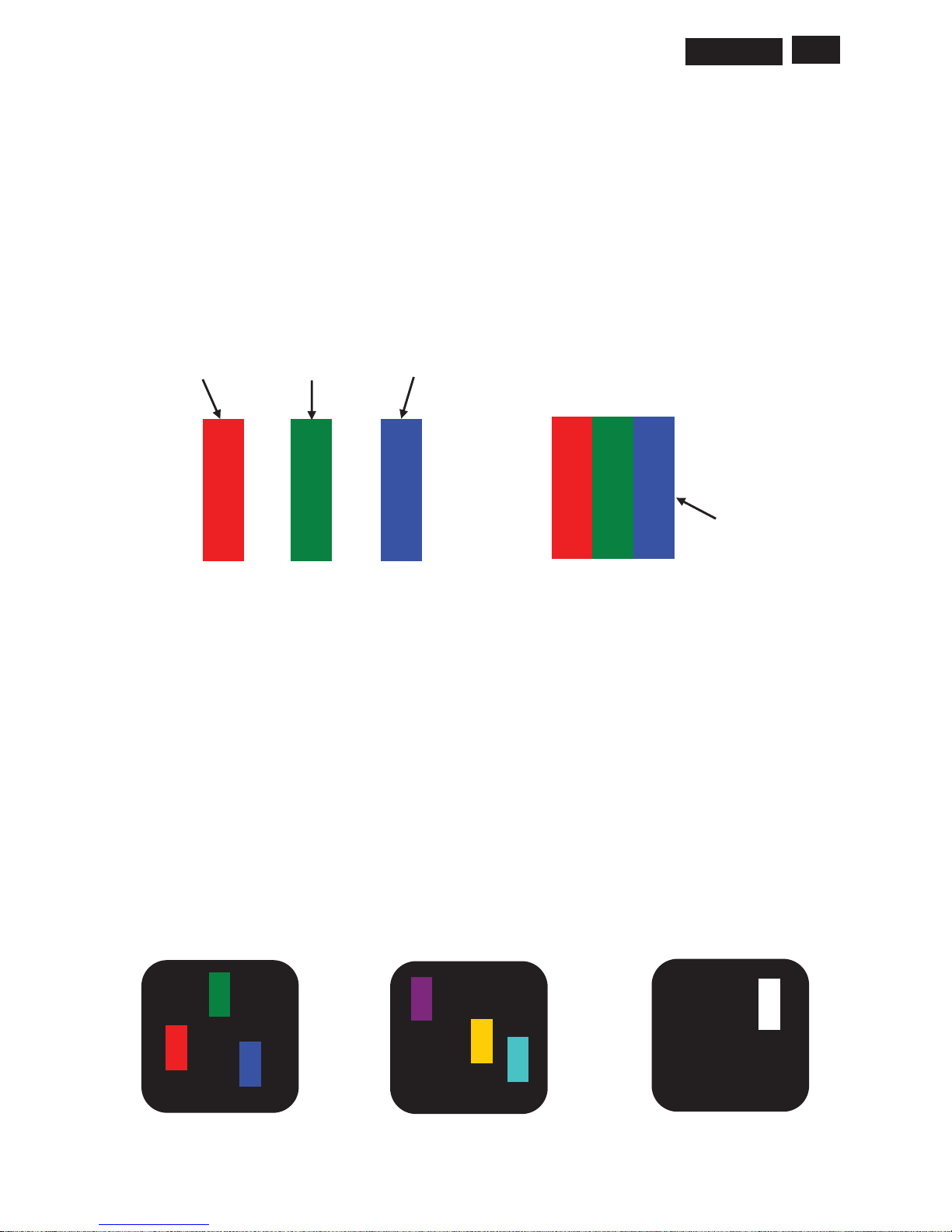
Pixels and Sub pixels
A pixel, or picture element, is composed of three sub pixels in the primary colors of red, green and blue. Many
pixels together form an image. When all sub pixels of pixel are lit, the three colored sub pixels together appear as a
single white pixel. When all are dark, the three colored sub pixels together appear as a signal black pixel. Other
combinations of lit and dark sub appear as single pixels of other colors.
Types of Pixel Defects
Pixel and sub pixel defects appear on the screen in different ways. There are two categories of pixel defects and
several types of sub pixel defects within each category.
Bright Dot Defects Bright dot defects appear as pixels or sub pixels that are always lit or ‘on’. That is, a Bright dot is
a sub-pixel that stands out on the screen when the monitor displays a dark pattern. There are three types of bright
dot defects:
R G B
R G B
subpixel
subpixel
subpixel
pixel
G
R
B
P
Y
C
W

!
!
Meridian 1
12
Two adjacent lit sub pixels:
- Red + Blue = Purple Three adjacent lit sub pixels
(one white pixel) One lit red, green or blue sub pixel - Red + Green = Yellow
- Green + Blue = Cyan (Light Blue)
A red or blue bright dot must be more than 50 percent brighter than neighboring dots while a green
bright dot is 30 percent brighter than neighboring dots.
Black Dot Defects Black dot defects appear as pixels or sub pixels that are always dark or ‘off’. That is, a dark dot
is a sub-pixel that stands out on the screen when the monitor displays a light pattern. There are two types of black
dot defects:
One dark sub pixel Two or three adjacent dark sub pixels
Proximity of Pixel Defects
Because pixel and sub pixels defects of the same type that are near to one another may be more noticeable,
Philips also specifies tolerances for the proximity of pixel defects.
Pixel Defect Tolerances
In order to qualify for repair or replacement due to pixel defects during the warranty period, a TFT LCD panel in a
Philips flat panel monitor must have pixel or sub pixel defects exceeding the tolerances listed in the following
tables.
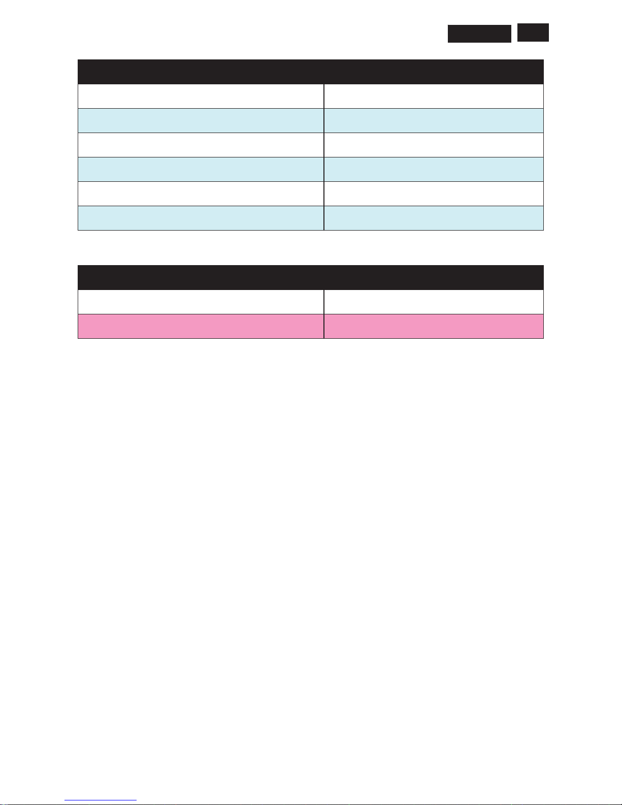
BRIGHT DOT DEFECTS ACCEPTABLE LEVEL
MODEL
160E1
1 lit subpixel 3
2 adjacent lit subpixels 1
3 adjacent lit subpixels (one white pixel) 0
Distance between two bright dot defects * >15mm
Total bright dot defects of all types 3
13
Meridian 1
BLACK DOT DEFECTS ACCEPTABLE LEVEL
MODEL
160E1
1 dark subpixel 5
2 adjacent dark subpixels 2
3 adjacent dark subpixels 0
Distance between two black dot defect s * >15mm
Total black dot defects of all types 5
TOTAL DOT DEFECTS ACCEPTABLE LEVEL
MODEL
160E1
Total bright or black dot defects of all types 5
Note:
* 1 or 2 adjacent sub pixel defects = 1 dot defect
!
!
Meridian 1
14
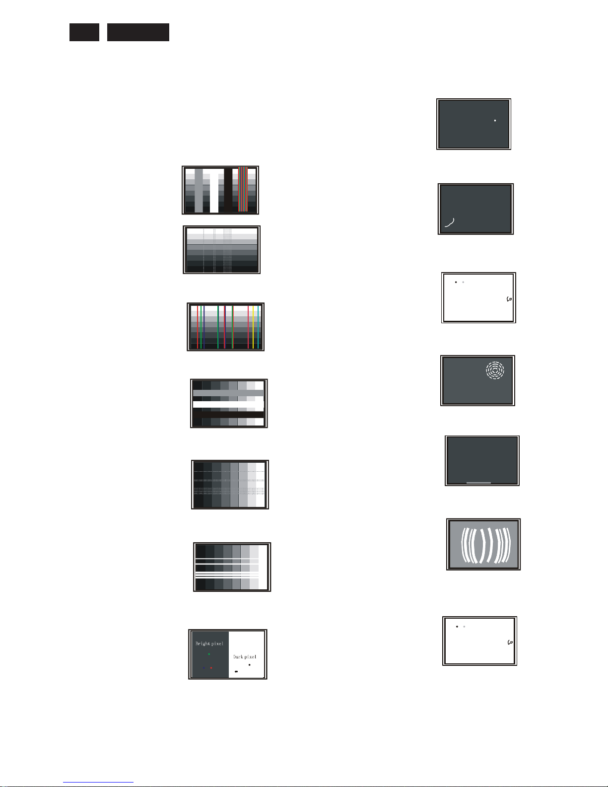
4.4 Failure Mode Of Panel
Failure description
Phenomenon
Vertical block defect
Vertical dim lines
Vertical lines defect
(Always bri
g
ht or dark)
Horizontal block defect
Horizontal dim lines
Horizontal lines defect
(Always bri
g
ht or dark)
Has bri
g
ht or dark pixel
Polarizer has bubbles
Polarizer has bubbles
Foreign material inside
polarizer. It shows liner or
dot shape.
Concentric circle formed
Bottom back light of LCD is
brighter than normal
Back light un-uniformity
Backli
g
ht has foreign material.
Black or white color, liner or
circular type
Quick reference for failure mode of LCD panel
this pa
g
e presents problems that could be made by LCD panel.
It is not necessary to repair circuit board. Simply follow the mechanical
instruction on this manual to eliminate failure by replace LC D panel.
15
Meridian 1
5. Block Diagram
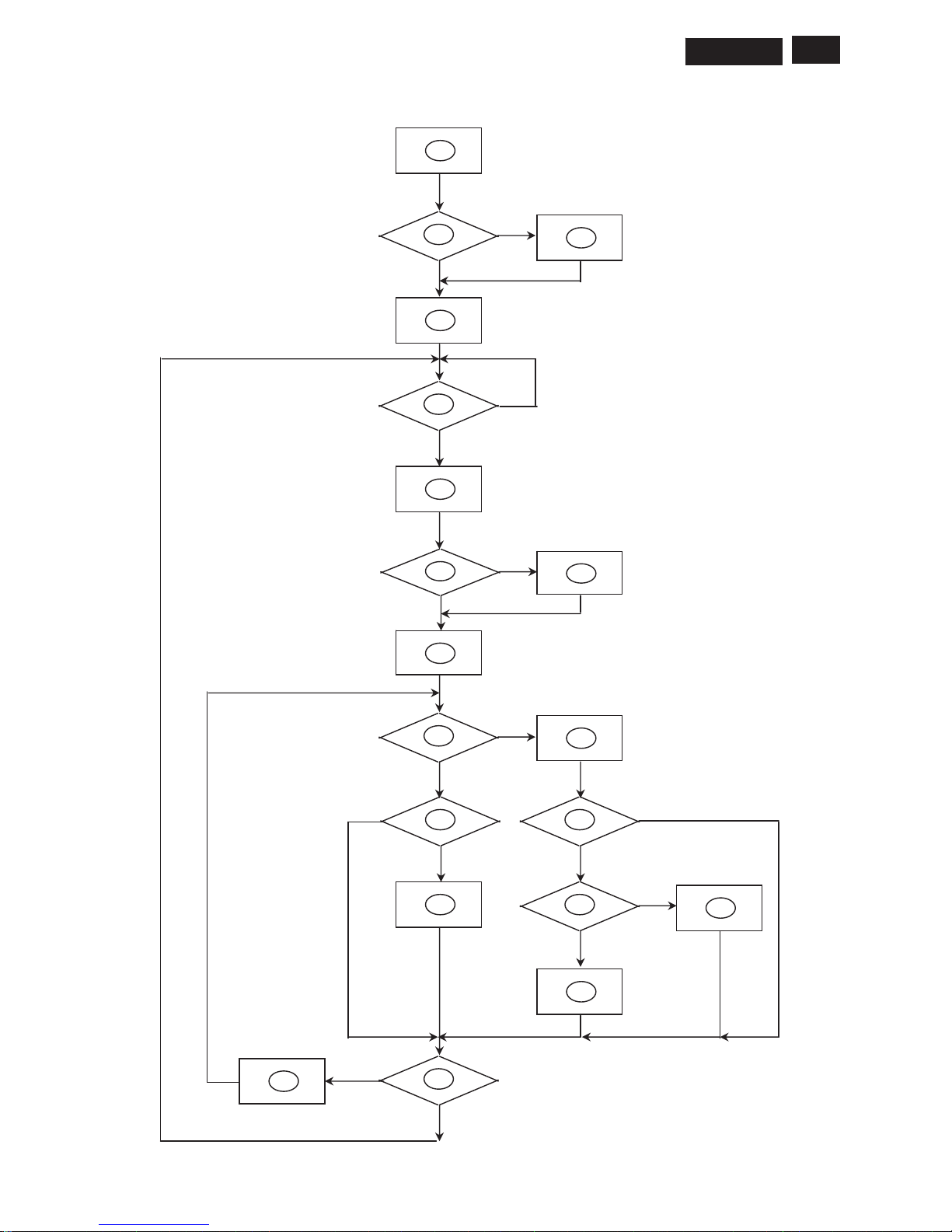
5.1 Software Flow Chat
1
2
N
Y
5
Y
N
10
Y
N
12
Y
N
7
Y
N
6
4
3
9
14
11
13
Y
N
15
Y
N
16
17
19
Y
N
18

!
!
Meridian 1
16
1) MCU initializes.
2) Is the EPROM blank?
3) Program the EPROM by default values.
4) Get the PWM value of brightness from EPROM.
5) Is the power key pressed?
6) Clear all global flags.
7) Are the AUTO and SELECT keys pressed?
8) Enter factory mode.
9) Save the power key status into EPROM.
Turn on the LED and set it to green color.
Scalar initializes
10) In standby mode?
11) Update the lifetime of back light.
12) Check the analog port, are there any signals coming?
13) Does the scalar send out an interrupt request?
14) Wake up the scalar.
15) Are there any signals coming from analog port?
16) Display "No connection Check Signal Cable" message. And go into standby mode after the message
disappears.
17) Program the scalar to be able to show the coming mode.
18) Process the OSD display.
19) Read the keyboard. Is the power key pressed?
17
Meridian 1
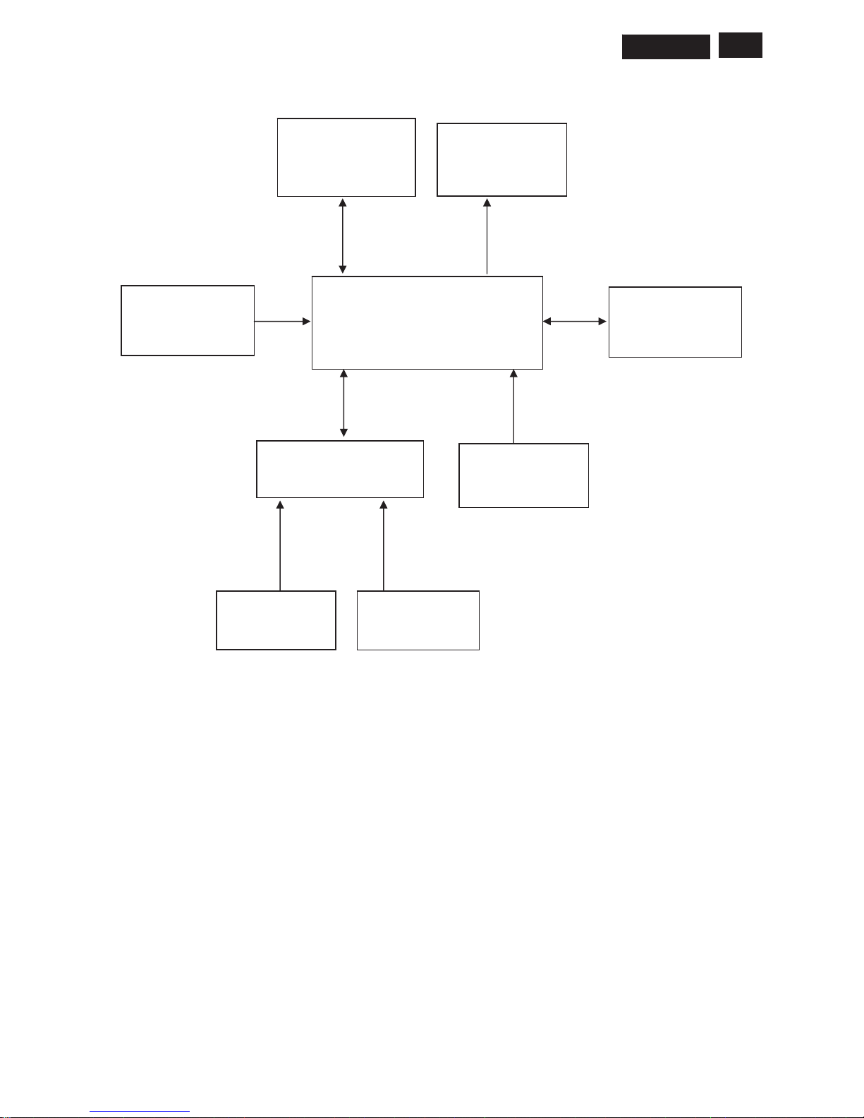
5.2 Electrical Block Diagram
5.2.1 Main Board
Flash Memory
PM25LV010A
(U402)
Panel Interface
(CN405)
Crystal 12MHz
(X401)
Keypad Interface
(CN401)
Scalar IC NT68167FG
(Include MCU, ADC, OSD)
(U401)
D-Sub Connector
(CN101)
ESD AZC099-04S
(U103)
H sync
V sync
RGB
ESD AZC099-04S
(U102)
VGA_R+
VGA_G+
VGA_B+
H_Sync
V_Sync
DSUB_SCL
DSUB_SDA
EEPROM
M24C16
(U407)
!
!
Meridian 1
18
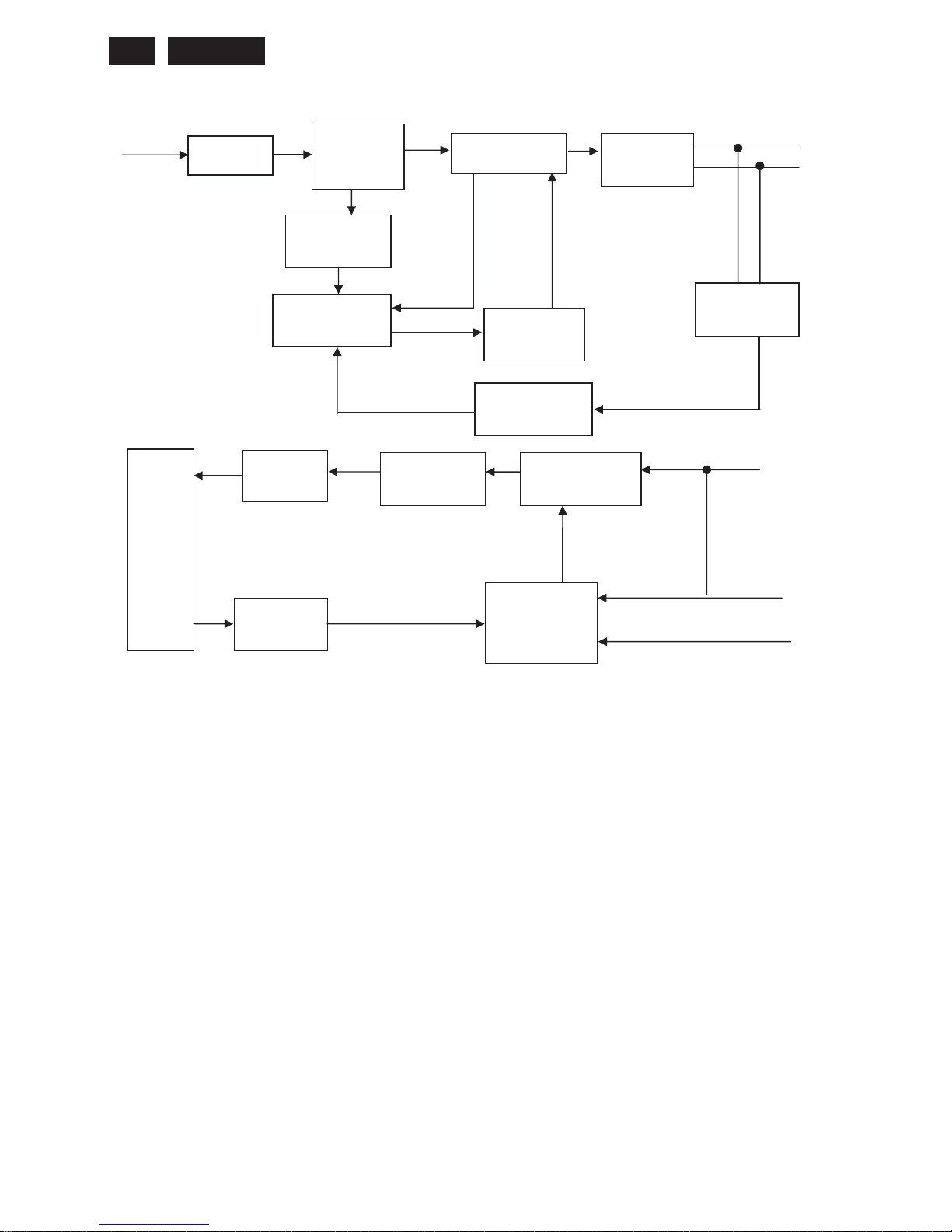
5.2.2 Power/Inverter Board
ON/OFF
EMI filter
Start Re sistor
(R904, R932)
PWM Control
(IC901)
Transformer
AC input
12V
Feedback
Circui
t
Transformer
(T801)
MOSFET
(Q802)
Lamp
5V
Bridge
Rectifier
and Filter
Feedback
Circuit
Rectifier
diodes
Output
Circui
t
PWM Control
TL494IDR
(IC801)
Power Switch
(Q901)
Photocoupler
(IC902)
12V
DIM
19
Meridian 1
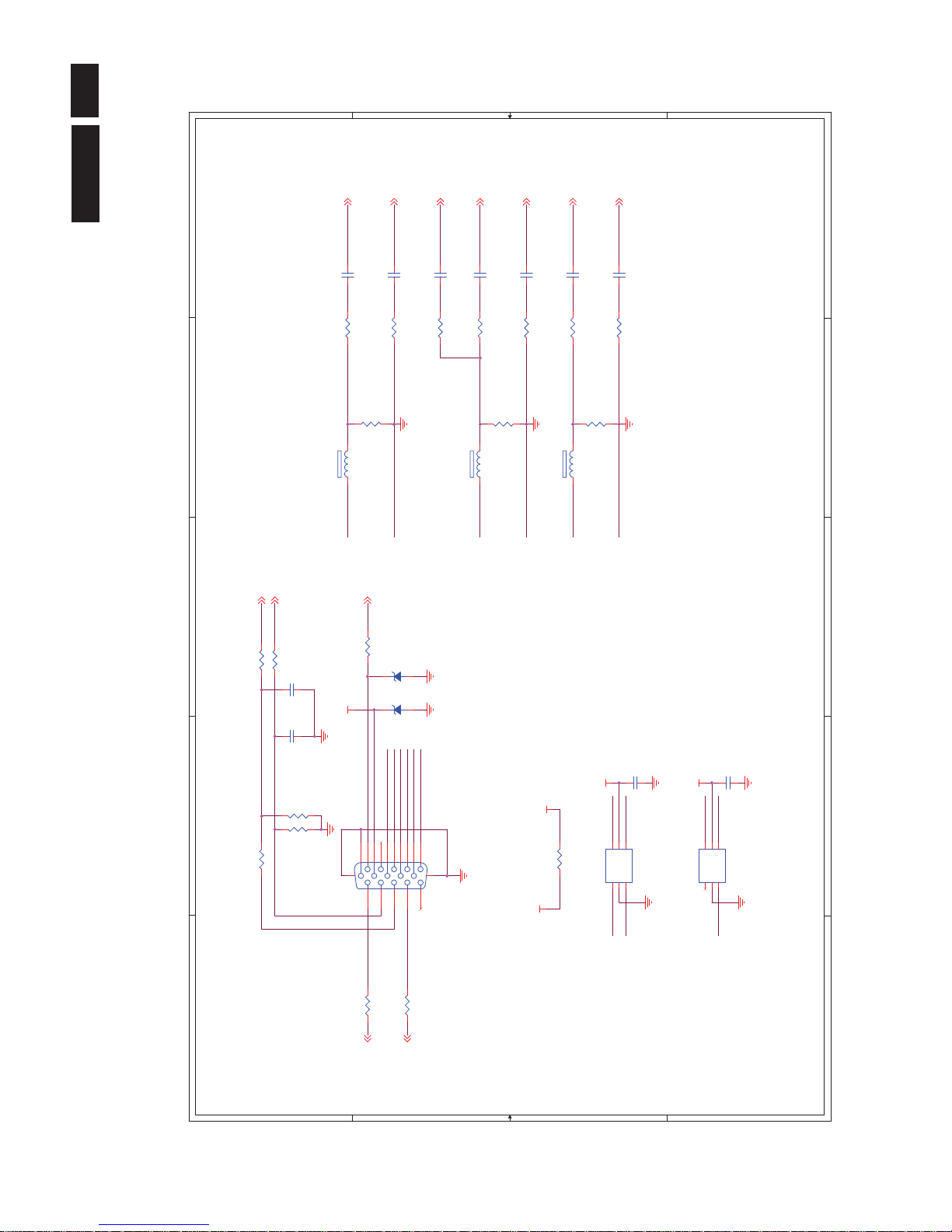
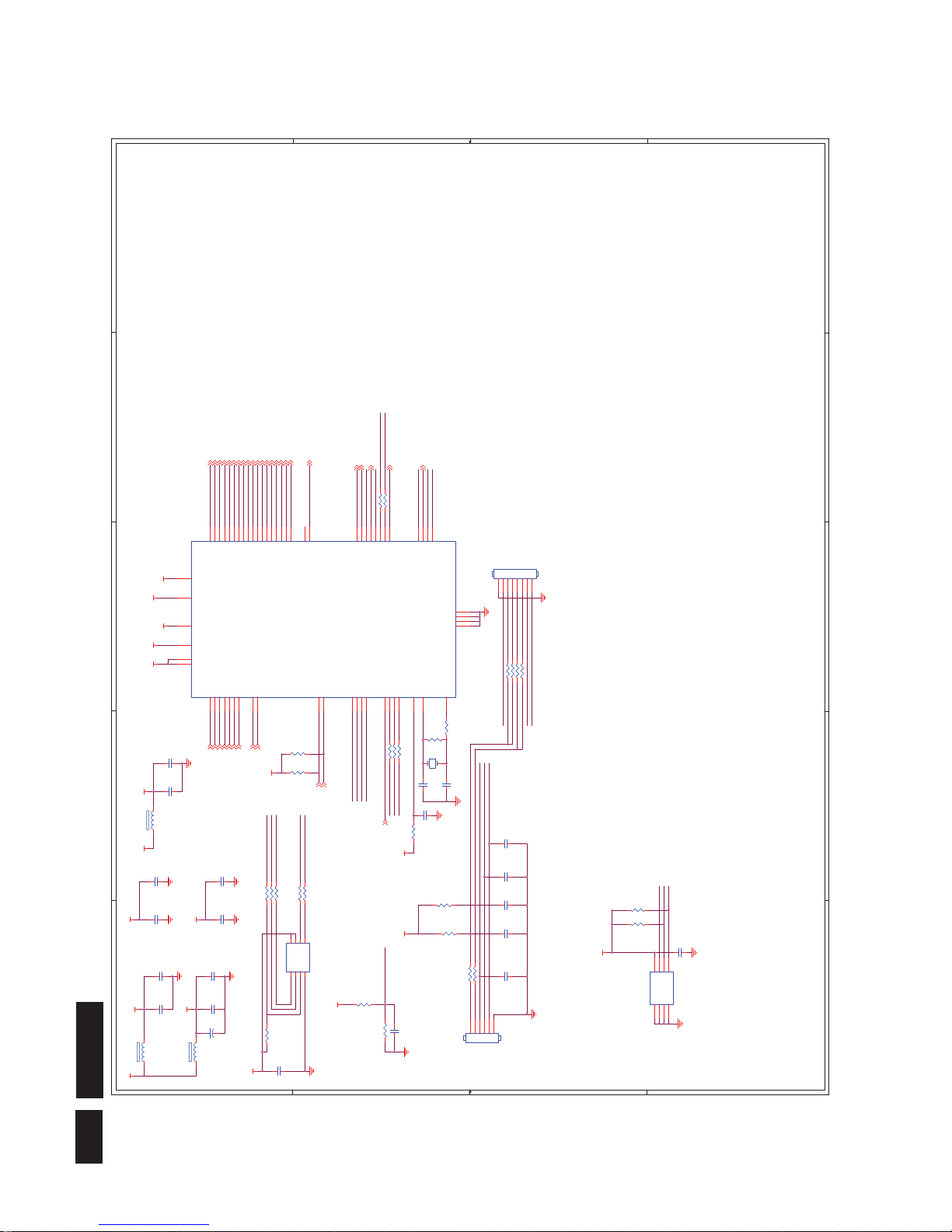
6. Schematic
6.1 Main Board
715G3213-F
1
1
2
2
3
3
4
4
5
5
A A
B B
C C
D D
CN101 A2
C101 A5
C102 A2
C103 A3
C105 B5
C106 B5
C107 B5
C109 C5
C110 C5
C113 C5
C114 D2
C115 C2
FB101 C4
FB102 A4
FB103 B4
R101 A2
R102 A3
R103 A3
R104 A4
R105 A2
R106 A2
R107 B4
R108 B4
R109 B4
R110 B1
R111 B4
R112 B4
R113 B1
R114 C4
R115 C4
R116 C4
R117 C4
R118 B3
R132 C2
U102 D2
U103 C2
ZD103 B2
ZD104 B3
INPUT
VGA_G-
V_Sync
H_Sync
VGA_B-
VGA_G+
VGA_R-
VGA_B+
VGA_B+
VGA_R+
DSUB_5V
VGA_G-
VGA_G+
DSUB_SCL
DSUB_SDA
VGA_R+
DSUB_SDAV_Sync
H_Sync
VGA_PLUG
VGA_R+
DSUB_SCL
VGA_B+
VGA_B-
VGA_R-
VGA_G+
BIN+ 2
BIN- 2
GIN+ 2
GIN- 2
SOGI 2
RIN- 2
RIN+ 2
VGA_DET 2
HSIN 2
VSIN 2
DDC_SDA2
DDC_SCL2
DSUB_5V
ESD_5V5VCC
ESD_5V
ESD_5V
C106
0.047uF
U102
AZC099-04S
123 4
5
6
I/O1
GND
I/O2 I/O3
VDD
I/O4
R118 10K 1/16W 5%
R117
100R 1/16W 5%
R110
100R 1/16W 5%
22pF
C103
ZD104
UDZSNP5.6B
1 2
C113
0.047uF
FB101
30 OHM
1 2
FB102
30 OHM
1 2
220pF
C102
R114
100R 1/16W 5%
R112
75R 1/16W 5%
U103
AZC099-04S
123 4
5
6
I/O1
GND
I/O2 I/O3
VDD
I/O4
R103 100R 1/16W 5%
C115
0.1uF/16V
R101 100R 1/16W 5%
R132
1K 1/16W 5%
CN101
DB15
162738495
11
12
13
14
15
10
17 16
R107
75R 1/16W 5%
R109
390 OHM 1/16W
C110
0.047uF
R113
100R 1/16W 5%
R111
100R 1/16W 5%
C109
0.047uF
C114
0.1uF/16V
C101
0.047uF
C107
0.047uF
R115
100R 1/16W 5%
R102 100R 1/16W 5%
FB103
30 OHM
1 2
R105
2K2 1/16W 5%
R116
75R 1/16W 5%
R106
2K2 1/16W 5%
R108
100R 1/16W 5%
ZD103
UDZSNP5.6B
1 2
C105
0.047uF
R104
100R 1/16W 5%
!
20
Meridian 1
1
1
2
2
3
3
4
4
5
5
A A
B B
C C
D D
Near to Connect
CN401 and CN402 layout together
CN401 B1
CN402 C3
C401 B2
C406 A2
C407 A2
C408 A1
C409 B1
C410 A1
C411 B2
C412 B2
C413 C1
C414 C1
C415 C1
C416 C2
C417 C2
C430 A2
C431 A2
C433 A1
C439 A1
C442 A1
C443 A1
C444 A1
C445 A1
C446 D1
FB404 A2
FB405 A1
FB407 A1
R405 A1
R406 B1
R408 A1
R409 B1
R410 B4
R414 B4
R416 B1
R417 B2
R418 B1
R419 B2
R422 A2
R423 A2
R427 B1
R428 B1
R429 C3
R430 C3
R431 C3
R432 C3
R449 A1
R450 B1
R451 B1
R452 A1
R462 B2
R463 B2
R464 B2
R465 B2
R466 C1
R467 C1
U401 A3
U402 A1
U407 C1
X401 B2
SCALAR
WP
LED_GRN/BLUE
LED_ORANGE
SPI_CE
SPI_SI
SPI_SO
KEY2
SPI_CK
5V_DET
5V_DET
KEY1
WP
POWER_KEY#
LED_GRN/BLUE
LED_ORANGE
KEY_RIGHT
POWER_KEY#
LED_GRN/BLUE
KEY_LEFT
KEY_AUTO
LED_ORANGE
KEY1
KEY2
POWER_KEY#
SPI_SO
SPI_CE
SPI_CK
SPI_SI
EE_WP
MSCL
MSDA
MSCL
MSDA
EE_WP
T1P 3
T0M 3
T2M 3
T0P 3
T2P 3
T1M 3
DDC_SDA1
DDC_SCL1
BIN-1
VSIN1
RIN+1
RIN-1
SOGI1
GIN+1
GIN-1
BIN+1
HSIN1
Volume# 4
Mute# 4
Panel_ID# 4
T4M 3
T3P 3
T3M 3
PANEL_EN 3
BL_ADJ 4
T4P 3
T6M 3
T7P 3
T5P 3
T7M 3
TCLK1M 3
T5M 3
T6P 3
TCLK1P 3
VGA_DET1
BL_ON
4
VCC3.3
DVDD
CVDD_1.8
+5V
ADC_1.8
ADC_2.3
CVDD_2.3
5VCC
DVDD
ADC_2.3
ADC_1.8
CVDD_2.3
CVDD_1.8
VCC3.3
VCC3.3 DVDD
VCC3.3
VCC3.3
R463
0R05 1/16W
C439
1uF 10V
C0402
C406
0.1uF/16V
R418 100R 1/16W 5%
C415
0.1uF/16V
R449 100R 1/16W 5%
R429 NC
C401
0.1uF/16V
+
C445
100UF25V
C416
0.1uF/16V
R467
4K7 1/16W 5%
C410
0.1uF/16V
C442
1uF 10V
C0402
R414 120R 1/16W 5%
R410 120R 1/16W 5%
R432 NC
C443
1uF 10V
C0402
R450 100R 1/16W 5%
R408
10K 1/16W 5%
R430 NC
R466
4K7 1/16W 5%
FB404
120 OHM
1 2
C446
0.22uF16V
R451 100R 1/16W 5%
C411 47pF
C414
0.1uF/16V
R465 100R 1/16W 5%
R422
4K7 1/16W 5%
FB405
300OHM
C430
0.1uF/16V
C409 100pF
C412 47pF
R417
1K 1/16W 5%
R462
1M 1/16W 5%
C413
0.1uF/16V
C431
0.1uF/16V
CN401
CONN
12345
6
CN402
NC/CONN
1234567
8
U402
PM25LV010A
123
4
876
5
CE#SOWP#
GND
VDD
HOLD#
SCK
SI
C444
1uF 10V
C0402
NT68167
U401
NT68167FG
18
11
13
45678
9
10
17
16
14
15
1
23
12
19 20
21
22
23
24
25
26
27
28
29
30
31
3233343537363938414043424544474649
48
50
51
52
53
54
55
56
57
58
596160
62
63
64
RSTB
DVDD_BIAS
MGND
BIN1+
BIN1-
SOG1I
GIN1+
GIN1-
RIN1+
RIN1-
PB5*/DDC_SDA*/TX
PB4*/DDC_SCL*/RX
HSYNCI1
VSYNCI1
ADC_2.3
ADC_1.8AGND
DVDD
P34 PA0/PWM2
PA1/PWM3
PB0/ADC0
PB1/ADC1
DGND
CVDD_2.3
CVDD_1.8
PA4*/PWM6*
PA5*/PWM7*
PWMA*
P30/RXD
P31/TXD
T7P
T7M
T6P
T6M
T5M
T5P
T4M
T4P
T3M
T3P
TCLK1M
TCLK1P
T2M
T2P
T1M
T1P
T0M
T0P
DGND
P35
PWMB*
PA7*/PWM9*
PA6*/PWM8*
PB3/ADC3
PB2/ADC2
PA3/PWM5
PA2/PWM4
SPI_CLK
SPI_SI
SPI_SO
SPI_CE
OSCI
OSCO
R452 100R 1/16W 5%
C417
0.1uF/16V
R409
4K7 1/16W 5%
C433
0.1uF/16V
R419 1K 1/16W 5%
R431 NC
R464 100R 1/16W 5%
R427
3.9K OHM +-1% 1/16W
R428
3.9K OHM +-1% 1/16W
R406
4K7 1/16W 5%
C407
0.1uF/16V
R416 100R 1/16W 5%
X401
12MHz
1 2
U407
M24C16
123
4 5
678
A0A1A2
GND SDA
SCL
WP
VCC
R405 100R 1/16W 5%
FB407
300OHM
C408
0.22uF16V
R423
4K7 1/16W 5%
21
Meridian 1
1
1
2
2
3
3
4
4
5
5
A A
B B
C C
D D
SD2
3
AO3401L
1
G
CN403 A5
CN405 A2
C419 C2
C420 A3
C421 C3
C441 C1
FB402 C3
Q404 C2
Q405 C3
R415 C1
R433 C2
R434 A3
R435 C1
R436 C2
OUTPUT
T0M2
T0P2
T1P2
T1M2
T2P2
T2M2
TCLK1M2
TCLK1P2
T3P2
T3M2
T4P2
T4M2
T5P2
T5M2
T6P2
T6M2
T7P2
T7M2
PANEL_EN2
TCLK1P2
TCLK1M2
T0M2
T0P2
T1M2
T1P2
T2M2
T2P2
TCLK1P2
TCLK1M2
T3M2
T3P2
+5V
PANEL_VCC
PANEL_VCC
PANEL_VCC
R433
10K 1/16W 5%
FB402
120 OHM
R436
10K 1/16W 5%
R435 10K 1/16W 5%
CN403
NC
123456789
101112131415161718192021222324252627282930
C441
0.1uF/16V
Q405
AO3401
R415
10K 1/16W 5%
C420
0.1uF/16V
CN405
CONN
246810121416182022
24
13579
1113151719
21
23
C419
1uF 10V
Q404
2N3904S-RTK/PS
+
C421
100UF25V
R434
220 OHM +-5% 1/4W
!
22
Meridian 1
1
1
2
2
3
3
4
4
5
5
A A
B B
C C
D D
POWER
CN404 A1
C422 B4
C425 D1
C426 B3
C427 B4
C428 B3
D401 A2
D403 A2
Q406 D1
R424 C2
R425 C3
R426 B2
R437 C1
R438 C3
R440 D1
R441 B2
R442 C1
R443 C2
R444 B3
R448 B2
R457 B1
U404 B4
U406 A4
Volume
BKLT-EN
BKLT-VBRI
C_PANEL_INDEX
BKLT-VBRI
Mute
Mute
C_PANEL_INDEX
BKLT-EN
BL_ADJ 2 Mute# 2
Volume# 2
Panel_ID# 2
BL_ON 2
VCC3.3
DSUB_5V
+5V
5VCC
VCC3.3 VCC3.3+5V
VCC3.3+5V
+5V
+5V
5VCC
C425
10K 1/16W 5%
R437
10K 1/16W 5%
R440
4K7 1/16W 5%
R424
NC/100R 1/16W 5%
R442
100R 1/16W 5%
+
C427
100UF25V
R425
NC
CN404
CONN
123456789
R426
NC
R441
10K 1/16W 5%
Q406
2N3904S-RTK/PS
R448
NC/100R 1/16W 5%
R457
NC
D403
SM240A
U404
AP1117D33LA
123
ADJ(GND)
VOUT
VIN
R438
NC
+
C426
100UF25V
C428
0.1uF/16V
R443
NC
U406 NC/AP1117E33LA
1
23
4
VSS
VOUTVIN
4
D401
BAT54C
C422
0.1uF/16V
R444
NC/10K 1/16W 5%

23
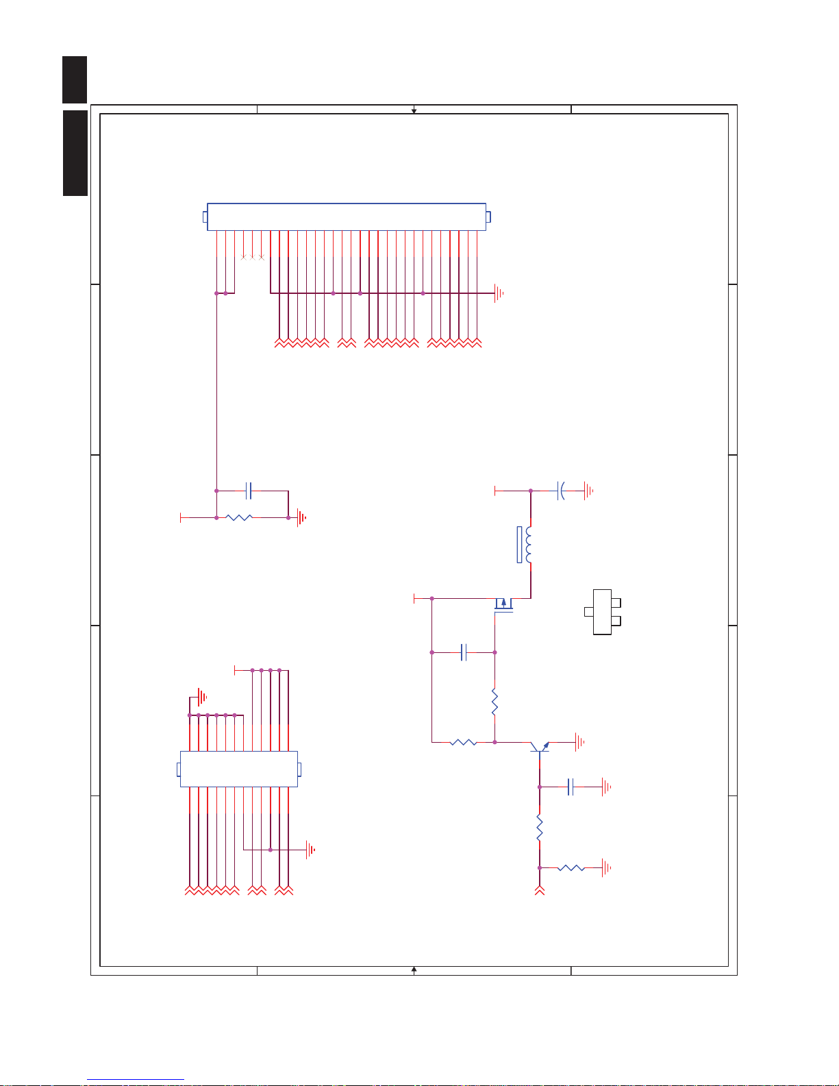
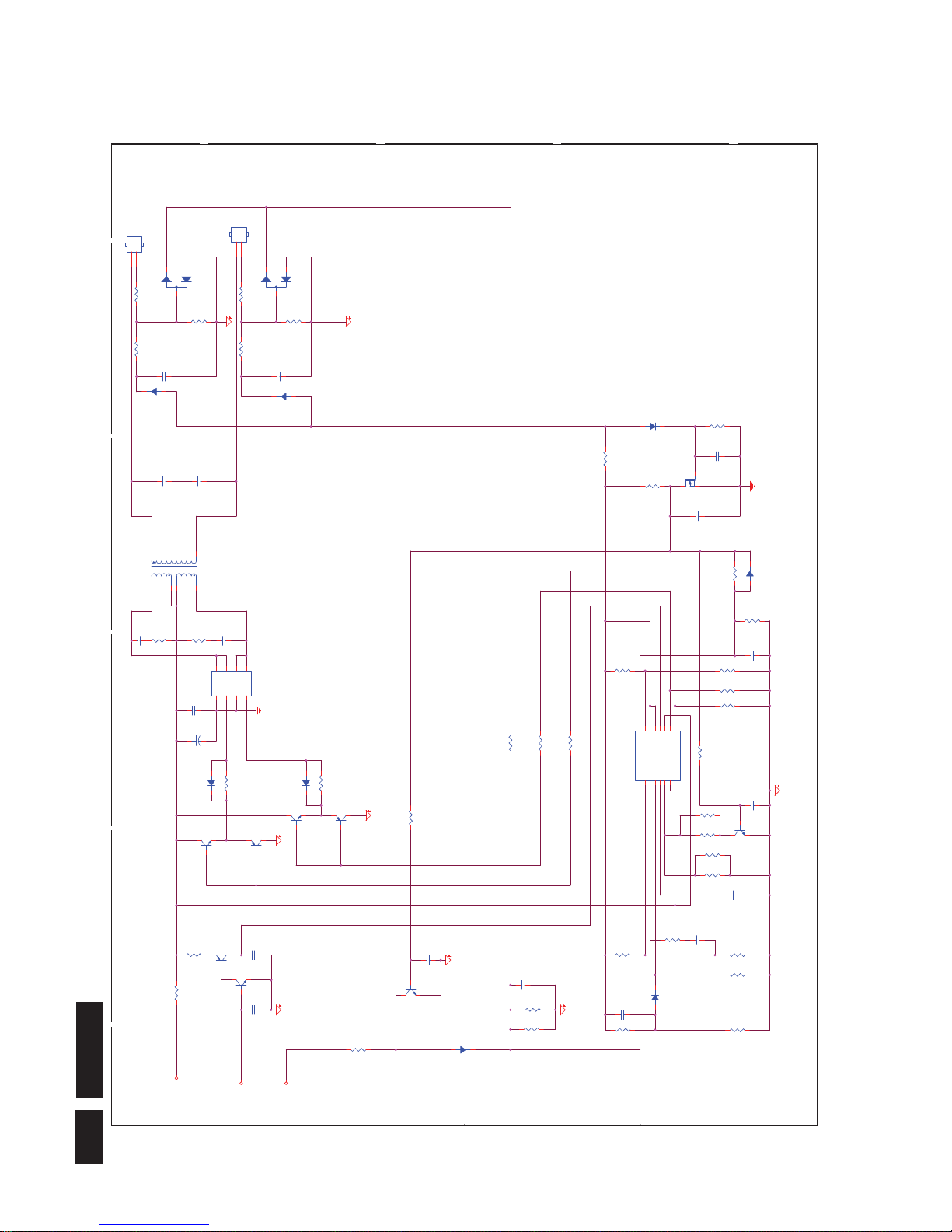
Meridian 1
6.2 Power Board
715G2852-2
1
1
2
2
3
3
4
4
5
5
A A
B B
C C
D D
!
!
!
!
!
N.C
!
!
!
!
!
!
!
!
!
!
!
!
BD901 A1 CN901 D1 CN902 C5 C900 C3 C901 B1 C902 B1
C903 B2 C904 A1 C906 A2 C907 A1 C908 B1 C909 C2
C910 A4 C911 B2 C912 A3 C915 B5 C917 A4 C918 A4
C921 A4 C922 A4 C924 C3 C925 C3 C928 C2 C929 B4
C930 A5 C931 D5 C932 A5 C938 A2 C939 A4 C940 B4
D900 A2 D901 A2 D903 B2 D905 B3 D906 A3 D907 A3
D915 C4 D916 C4 F901 D1 F902 A5 F903 B5 F904 B5
F905 B5 GND1 C2 HS2 D2 HS3 D2 HS5 D2 IC901 B2
IC902 C3 IC903 C3 L901 B1 L903 B4 L904 A4 L905 A4
NR901 C1 01(NC) C1 Q901 B2 Q903 A5 Q904 B4 R900 C1
R901 C1 R902 C1 R904 A2 R905 A2 R906 A2 R907 B2
R908 A2 R909 A2 R910 B2 R912 B2 R914 B2 R915 B1
R918 A3 R919 A3 R920 A3 R921 A3 R922 A3 R923 B3
R924 B4 R925 C3 R926 C3 R927 B4 R930 C4 R932 A2
R935 B3 R938 B2 R939 A5 R940 B5 R942 C4 R943 A5
R946 A5 R947 A4 R948 A4 R952 B4 R961 B3 R962 B3
T901 A3 VAR901 C1 ZD902 A5 ZD905 B2 ZD921 B4 ZD922 B4
POWER
+12V
+5V
+5V1
+5V
DIM
ON/OFF
VOL
MUTE
F903
NC
D900
FR107
C928
0.01uF
R948
NC
C909
470pF/25V
R939
1K 1/8W
R920
100 OHM 1/4W
C902
1000pF
Q904
NC
R923 NC
R962 100 OHM 1/4W
D906
FCH10U10
1
2
3
GND1
GND
1
2
D901
FR103
R925
1K 1/8W
C911
0.1uF
C901
1000pF
C908
0.22uF/275V
HS3
HEAT SINK(Q901_Q90G6263-6)
1
2
C932
0.001uF
+
C903
22uF/50V
ZD902
RLZ13B
1 2
+
C922
470PF50V
+
C915
470uF/16V
R914
0.47 OHM +-5% 2WS
+
C907
100uF450V
CN901
87G 501 32 DL
SOCKET
12
3
L901
30mH
1
4
2
3
HS2
HEAT SINK(D906_Q90G6263-6)
1
2
C912
0.001uF
T901
POWER X'FMR
789
10
11
12
4
5
612
R932
10K OHM 1/4W
R961 100 OHM 1/4W L903
1.0uH
D915
LL4148
R910
10R 1/4W
R909
5.1 OHM 1/4W
R900
680K OHM 1/4W
R940
33K 1/10W
R930
2.43K OHM 1% 1/10W
L905
NC
L904
1.0uH
R924
150R 1/8W
IC902
PC123X2YFZOF
12
43
D916
LL4148
R902
680K OHM 1/4W
R912
220 OHM 1/4W
+
C917
680uF/25V
+
C940
1000UF25V
C904
0.22uF/275V
C924
0.1uF
R907
NC
C938
NC
R921
NC
+
C918
680uF/25V
R915
100K OHM 1% 1/8W
R935 100 OHM 1/4W
R918
100 OHM 1/4W
R926
1K 1/10W 1%
R942
1K 1/10W 1%
D903
LL4148
F901
FUSE
+
C921
NC
R901
680K OHM 1/4W
VAR901
Varistor
R905
NC
IC903
AZ431AZ-AE1
R906
NC
+
C939
NC
R927
3.6K OHM 1% 1/10W
D907 NC
R952
NC
C931
0.1uF
F902
NC
Q903
PMBS3904
C900
3300pF 250V
ZD921
RLZ13B
1 2
t
NR901
NTCR
12
R904
10K OHM 1/4W
C925
NC
C930
0.1uF
IC901
LD7575A PS
123
4 5
678
RT
COMPCSGNDOUT
VCC
NC
HV
t
NR901(NC)
NTCR
12
R919
100 OHM 1/4W
ZD922
RLZ5.1B
1 2
ZD905
RLZ18B
1 2
C929
0.001uF
D905 31DQ06FC3
C910
NC
R943
470R 1/8W
HS5
SHIELD(H85G0002-1)
1
2
-
+
BD901
KBP208G
2
1
3
4
Q901
2SK2645-54MR
R908
100KOHM +-5% 2WS
C906
1500pF2KV
CN902
CONN
123456789
10
R922
NC
F904
NC
R947
NC
R938
10K 1/8W
ZD923
NC
1 2
R946
150 OHM 2W
F905
0 OHM 1/4W
!
24
Meridian 1
1
1
2
2
3
3
4
4
5
5
A A
B B
C C
D D
〱㊸
ᮄ
CN801 A5
CN802 A5
C801 A4
C802 A2
C803 A4
C807 A1
C817 D2
C819 A4
C820 D2
C821 D1
C822 C1
C823 A4
C824 A3
C825 A1
C834 D4
C835 B1
C838 A3
C839 A3
C842 C1
C845 D3
C846 D4
D801 A5
D802 A5
D805 A4
D806 C4
D807 A4
D810 A2
D811 B2
D812 D1
D814 D3
D817 B1
F801 A1
IC801 C2
Q801 A2
Q802 A3
Q804 A2
Q805 A1
Q806 B1
Q807 D2
Q808 A1
Q809 D4
Q811 B2
Q812 B2
R801 A5
R802 C1
R803 D3
R804 A1
R807 C3
R808 D3
R810 D2
R814 A5
R817 A4
R818 C4
R820 D1
R821 A5
R822 A5
R823 D1
R824 D3
R825 C2
R826 D3
R827 B1
R828 A4
R829 C2
R830 C1
R831 D1
R832 C1
R835 D4
R837 C4
R839 A2
R841 C2
R850 B2
R851 C1
R853 B2
R854 D2
R855 A3
R856 A3
R861 D2
R862 D3
R863 D1
R864 D2
R865 D2
T801 A3
INVERTER
+12V
ON/OFF
DIM
C825
0.1uF/25V
F801
0 OHM 1/4W
Q804
PMBS3906
1
23
C835
NC
R832
10K 1/10W 1%
D802
BAV99
3
1
2
CN802
CONN
1
2
R818
1K 1/10W 1%
D811
NC
R814
1K5 1/10W 1%
D812
LL4148
R803
680K 1/10W
R835
1M 1/10W 5%
D806
LL4148
R822
1K 1/8W
C838
1500PF/50V
R817
10K 1/10W 1%
R851
6K8 1/10W
C801
30pF/3KV
R821
1K 1/8W
R839
22R 1/8W
C834
0.1uF/25V
R861
NC
R826
1K 1/8W
R810
51K OHM 1% 1/8W
C821
0.1uF/25V
IC801
TL494IDR
1234567
8 9
10111213141516
1IN+
1IN-
FEEDBACK
DTCCTRT
GND
C1 E1
E2
C2
VCC
OUTPUT CTRL
REF
2IN-
2IN+
R820
10K 1/10W 1%
C807
0.1uF/25V
Q806
PMBS3904
C823
0.0022uF
R808
10K 1/10W 1%
+
C802
470PF50V
C845
2.2uF/16V
R856
15R 1/4W
R837
47K 1/8W
R801
1K5 1/10W 1%
R854
NC
D817
LL4148
Q809
RK7002
D805
LL4148
Q812
PMBS3906
1
23
R830
NC
CN801
CONN
1
2
R825
22R 1/8W
C803
30pF/3KV
D807
LL4148
C824
0.1uF
D814
LL4148
R807
10K 1/10W 1%
R853
68K 1/10W
C820
220pF50V
R824
1K 1/10W 1%
Q801
PMBS3904
C817
NC
D801
BAV99
3
1
2
R841
68K OHM 1% 1/10W
Q802
AM9945N-T1-PF
123
4
876
5
SGS
G
DDD
D
R850
22R 1/8W
R802
8.2K 1/10W 1%
R831
1K 1/8W
Q808
PDTA144WK
R862
1M 1/10W 5%
R823
0R05 1/10W 5%
R829
22R 1/8W
C842
0.01uF
Q805
PDTC144WK
R828
10K 1/10W 1%
R855
15R 1/4W
R864
NC
C819
0.0022uF
Q811
PMBS3904
R863
10K 1/10W 1%
R865
NC
C846
NC
R827
1K 1/10W 1%
R804
100R 1/8W
T801
POWER X'FMR
6
374
81
D810
NC
C822
1uF/25V
Q807
N.C
C839
1500PF/50V
25
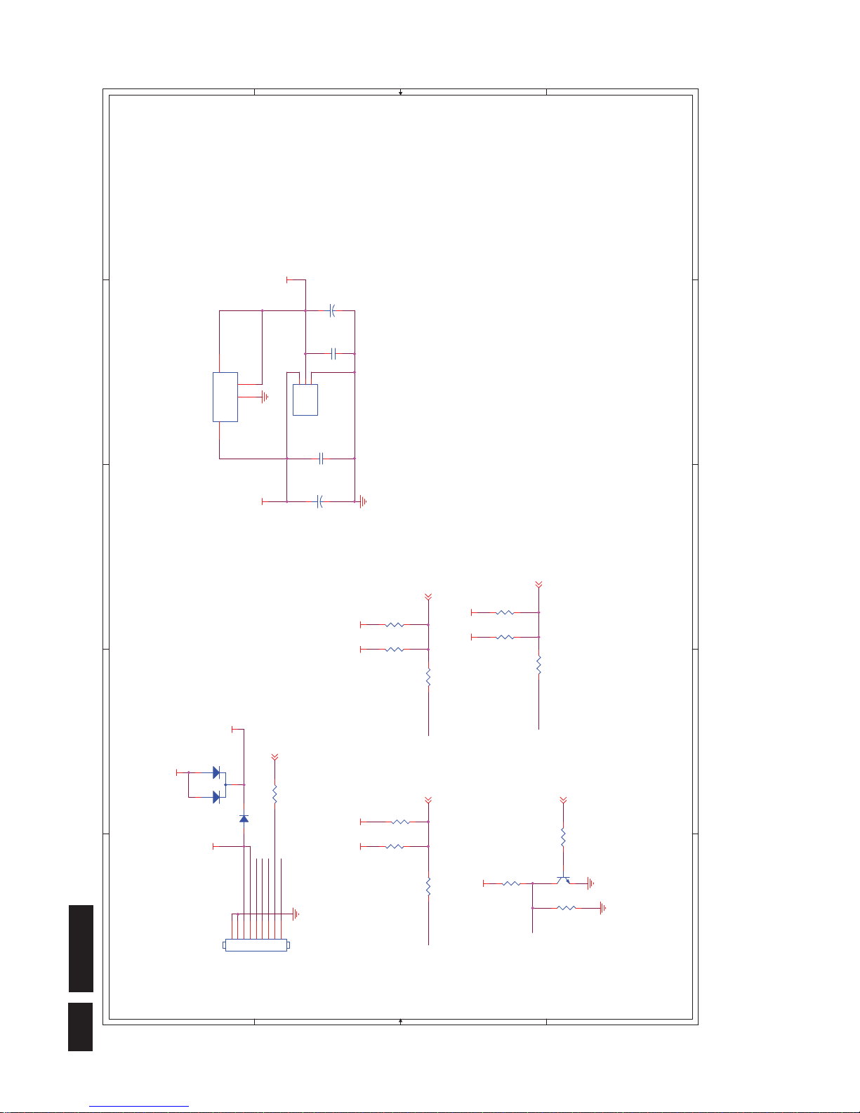
Meridian 1
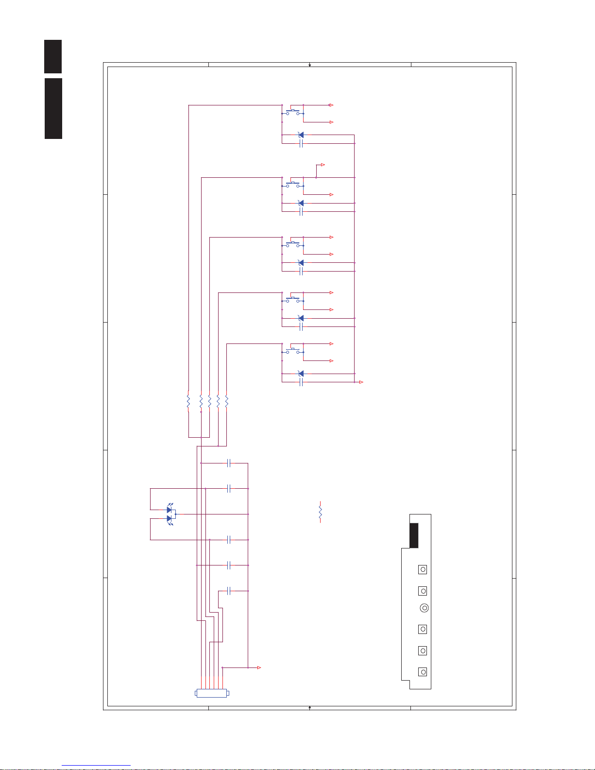
6.3 Key Board
715G3016-1
1
1
2
2
3
3
4
4
5
5
A A
B B
C C
D D
(OK)(UP) (DOWN)
CONNECTOR
(MENU) LED(Power)
KEY-PAD-SWITCH
CN001 A1
C001 B1
C002 B2
C003 B2
C004 B2
C005 B2
C006 B4
C007 B3
C008 B3
C009 B4
C010 B5
LED001 A2
R001 A3
R002 A3
R004 B3
R005 B3
R007 C2
SW001 B4
SW002 B4
SW003 B5
SW004 B4
SW005 B3
ZD001 B4
ZD002 B3
ZD003 B5
ZD004 B3
ZD005 B4
OK
LED_RED#
LED_GRN#
LED_GRN#
LBADC1
LBADC2
DC_POWERON
MENU
POWER
DOWN
UP
GND
SGND SGND
SGND
SGND
SGND SGND SGNDSGND SGND SGNDSGND
ZD004NC/UDZS5.6B
C006NC/0.1uF
CN001
CONN
12345
6
C007NC/0.1uF
R007 0R05 1/4W
R001 4.3K OHM 1% 1/8W
C004
NC/0.001uF
C010NC/0.1uF
R003 910R 1/8W
LED001
LED
1
3
2
C009NC/0.1uF
C001
NC/0.001uF
SW001
SW
21
3 4
5
ZD003NC/UDZS5.6B
C005
NC/0.001uF
ZD002NC/UDZS5.6B
C008NC/0.1uF
C002
NC/0.001uF
C003
NC/0.001uF
SW002
SW
21
3 4
5
SW004
SW
21
3 4
5
ZD005NC/UDZS5.6B
SW003
SW
21
3 4
5
R005 2.4K OHM 1% 1/8W
R002 2.4K OHM 1% 1/8W
SW005
SW
21
3 4
5
R004 4.3K OHM 1% 1/8W
ZD001NC/UDZS5.6B
!
26
Meridian 1
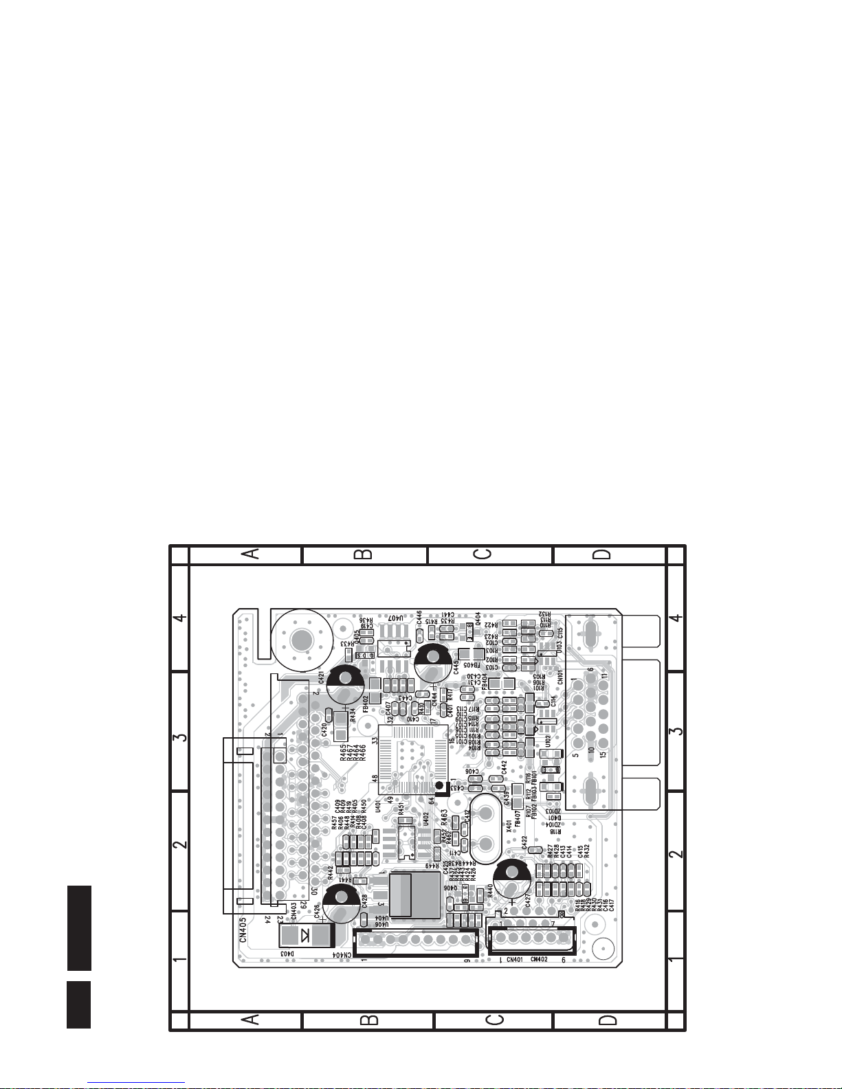
7. PCB Layout
7.1 Main Board
715G3213-F
C101 C3 C422 C2 FB404 C3 R408 B2 R441 B2
C102 C4 C425 C2 FB405 C4 R409 B2 R442 B2
C103 C3 C426 B2 FB407 C2 R410 C3 R443 C1
C105 C3 C427 C2 Q404 C4 R414 B2 R444 C2
C106 C3 C428 B1 Q405 B4 R415 C4 R448 B2
C107 C3 C430 C3 Q406 C2 R416 C2 R449 C2
C109 C3 C431 C3 R101 C3 R417 C3 R450 B2
C110 C3 C433 C2 R102 C4 R418 C2 R451 B2
C113 C3 C439 C2 R103 C4 R419 B2 R452 C2
C114 C3 C441 C4 R104 C3 R422 C4 R457 B2
C115 C4 C442 C3 R105 C4 R423 C4 R462 C2
C401 C3 C443 B3 R106 C4 R424 C1 R463 C2
C406 C3 C444 B3 R107 C3 R425 C1 R464 B3
C407 B3 C445 C4 R108 C3 R426 C1 R465 B3
C408 B2 C446 B4 R109 C3 R427 C2 R466 B3
C409 B2 CN101 D3 R110 C4 R428 C2 R467 B3
C410 B3 CN401 C1 R111 C3 R429 C2 U102 C3
C411 C2 CN402 C1 R112 C3 R430 D2 U103 C4
C412 C2 CN403 B2 R113 C4 R431 D2 U401 B3
C413 C2 CN404 B1 R114 C3 R432 D2 U402 B2
C414 D2 CN405 A2 R115 C3 R433 B4 U404 B2
C415 D2 D401 D3 R116 C3 R434 B3 U406 B2
C416 D2 D403 B1 R117 C3 R435 C4 U407 B4
C417 D2 FB101 C3 R118 C2 R436 B4 X401 C2
C419 B4 FB102 C3 R132 C4 R437 C1 ZD103 C3
C420 B3 FB103 C3 R405 B2 R438 C2 ZD104 C3
C421 B3 FB402 B3 R406 B2 R440 C2
 Loading...