

Philips 42PFL6158K/12, 42PFL7108K/12, 42PFL6158S/12, 40PFL8008S/60, 42PFL6188K/12 Service Manual
...Page 1
Colour Television Chassis
QFU1.2E
LA
Contents Page
1. Revision List 2
2. Technical Specs, Diversity, and Connections 2
3. Precautions, Notes, and Abbreviation List 7
4. Mechanical Instructions 11
5. Service Modes, Error Codes, and Fault Finding 20
6. Alignments 40
7. Circuit Descriptions 45
8. IC Data Sheets 47
9. Block Diagrams 49
10. Circuit Diagrams and PWB Layouts Drawing PWB
310431366124 SSB
59
99-100
310431366185 SSB 101
141-142
310431366186 SSB 143
183-184
C 310431366652 Amplifier panel 185
272217190763, 272217190764, 272217190766
Keyboard Control Module 187
282206502664, 282206502665, 820400159661
Page 2
Revision List
EN 2 QFU1.2E LA1.
1. Revision List
Manual xxxx xxx xxxx.0
• First release.
Manual xxxx xxx xxxx.1
• Chapter 2: Table 2-1
updated (added CTNs).
• Chapter 4: added additional Ambilight unit handling info;
see section 4.3.2
.
Manual xxxx xxx xxxx.2
• Chapter 2: Table 2-1
updated (added CTNs).
Manual xxxx xxx xxxx.3
• Chapter 2: Table 2-1
updated (added CTNs).
• Chapter 6: added white tone values; see section 6.3.1
.
Manual xxxx xxx xxxx.4
• Chapter 2: Table 2-1
updated (added CTNs).
• Chapter 4: updated and added cable wiring (added CTNs).
• Chapter 6: added white tone values (added CTNs).
• Chapter 9: added wiring diagrams (added CTNs).
• Chapter 10: added schematics (AL).
• Chapter 11: added styling sheets (added CTNs).
2. Technical Specs, Diversity, and Connections
Index of this chapter:
2.1
Technical Specifications
2.2 Directions for Use
2.3 Connections
2.4 Chassis Overview
Notes:
• Figures can deviate due to the different set executions.
• Specifications are indicative (subject to change).
2.1 Technical Specifications
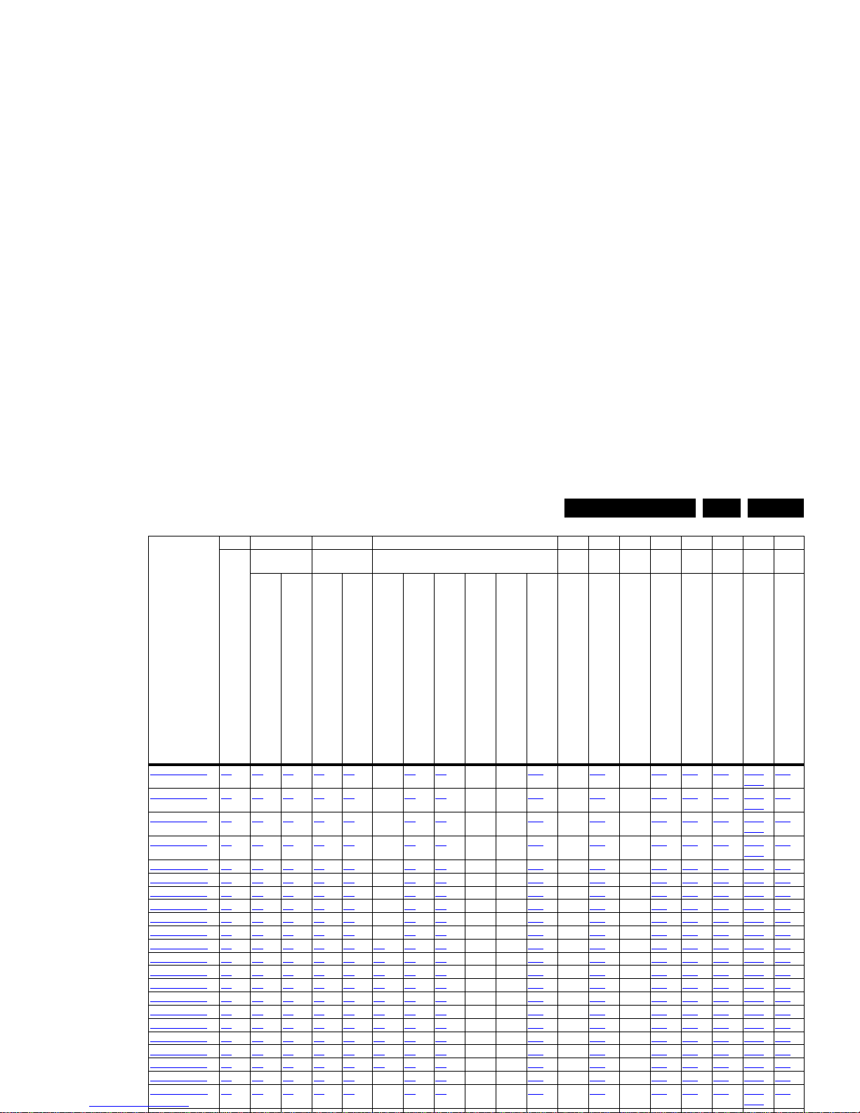
For on-line product support please use the CTN links in Table
2-1. Here is product information available, as well as getting
started, user manuals, frequently asked questions and
software & drivers.
Table 2-1 Described Model Numbers and Diversity
2 4 7 9 10 11
Mechanics Descr. Block Diagrams
Schem
atics Styling
Page 3
Technical Specs, Diversity, and Connections
EN 3QFU1.2E LA 2.
42PFL7108K/12 2.3 4-4 4.3 7.2 7.3 - 9.9 9.9 - - 9.10 - 10.2 - 10.5 10.7 10.9 10.11
10.12
11.2
42PFL7108S/12 2.3 4-4 4.3 7.2 7.3 - 9.9 9.9 - - 9.10 - 10.2 - 10.5 10.7 10.9 10.11
10.12
11.2
42PFL7108S/60 2.3 4-4 4.3 7.2 7.3 - 9.9 9.9 - - 9.10 - 10.2 - 10.5 10.7 10.9 10.11
10.12
11.2
42PFL7108T/12 2.3 4-4 4.3 7.2 7.3 - 9.9 9.9 - - 9.10 - 10.2 - 10.5 10.7 10.9 10.11
10.12
11.2
46PDL8908S/12 2.3 4-7 4.3 7.2 7.3 - 9.9 9.9 - - 9.10 - 10.1 - 10.5 10.8 10.9 10.12 11.4
46PDL8908S/60 2.3 4-7 4.3 7.2 7.3 - 9.9 9.9 - - 9.10 - 10.1 - 10.5 10.8 10.9 10.12 11.4
46PFL8008K/12 2.3 4-5 4.3 7.2 7.3 - 9.9 9.9 - - 9.10 - 10.1 - 10.5 10.7 10.9 10.15 11.3
46PFL8008S/12 2.3 4-5 4.3 7.2 7.3 - 9.9 9.9 - - 9.10 - 10.1 - 10.5 10.7 10.9 10.15 11.3
46PFL8008S/60 2.3 4-5 4.3 7.2 7.3 - 9.9 9.9 - - 9.10 - 10.1 - 10.5 10.7 10.9 10.15 11.3
46PFL8008S/98 2.3 4-5 4.3 7.2 7.3 - 9.9 9.9 - - 9.10 - 10.1 - 10.5 10.7 10.9 10.15 11.3
47PFL6008H/12 2.3 4-3 4.3 7.2 7.3 9.2 9.9 9.9 - - 9.10 - 10.2 - 10.5 10.7 10.9 10.15 11.1
47PFL6008K/12 2.3 4-3 4.3 7.2 7.3 9.2 9.9 9.9 - - 9.10 - 10.2 - 10.5 10.7 10.9 10.15 11.1
47PFL6008S/12 2.3 4-3 4.3 7.2 7.3 9.2 9.9 9.9 - - 9.10 - 10.2 - 10.5 10.7 10.9 10.15 11.1
47PFL6008S/60 2.3 4-3 4.3 7.2 7.3 9.2 9.9 9.9 - - 9.10 - 10.2 - 10.5 10.7 10.9 10.15 11.1
47PFL6158K/12 2.3 4-3 4.3 7.2 7.3 9.2 9.9 9.9 - - 9.10 - 10.2 - 10.5 10.7 10.9 10.15 11.1
47PFL6158S/12 2.3 4-3 4.3 7.2 7.3 9.2 9.9 9.9 - - 9.10 - 10.2 - 10.5 10.7 10.9 10.15 11.1
47PFL6188K/12 2.3 4-3 4.3 7.2 7.3 9.2 9.9 9.9 - - 9.10 - 10.2 - 10.5 10.7 10.9 10.15 11.1
47PFL6188S/12 2.3 4-3 4.3 7.2 7.3 9.2 9.9 9.9 - - 9.10 - 10.2 - 10.5 10.7 10.9 10.15 11.1
47PFL6198K/12 2.3 4-3 4.3 7.2 7.3 9.2 9.9 9.9 - - 9.10 - 10.2 - 10.5 10.7 10.9 10.15 11.1
47PFL6678K/12 2.3 4-3 4.3 7.2 7.3 9.2 9.9 9.9 - - 9.10 - 10.2 - 10.5 10.7 10.9 10.15 11.1
47PFL6678S/12 2.3 4-3 4.3 7.2 7.3 - 9.9 9.9 - - 9.10 - 10.2 - 10.5 10.7 10.9 10.15 11.1
47PFL7008H/12 2.3 4-4 4.3 7.2 7.3 - 9.9 9.9 - - 9.10 - 10.2 - 10.5 10.7 10.9 10.12
10.13
11.2
CTN
24 7 9 10 11
Connection Overview
Mechanics Descr. Block Diagrams
Schem
atics Styling
Wire Dressing
Assembly Removal
Power Supply
General Power Architecture
Wiring Diagram
Video
Audio
Control & Clock
I2C
Supply lines
Power Supply
SSB
Amplifier control module
(Keyboard Control Module)
(Wireless LAN USB, Light Sensor, IR/LED Module)
(Sensor Module)
(AmbiLight)
Sheet
Page 4

Technical Specs, Diversity, and Connections
EN 4 QFU1.2E LA2.
55PFL6188S/12 2.3 4-3 4.3 7.2 7.3 9.3 9.9 9.9 - - 9.10 - 10.2 - 10.5 10.8 10.9 10.16 11.5
55PFL6198K/12 2.3 4-3 4.3 7.2 7.3 9.3 9.9 9.9 - - 9.10 - 10.2 - 10.5 10.8 10.9 10.16 11.5
55PFL6678K/12 2.3 4-3 4.3 7.2 7.3 9.3 9.9 9.9 - - 9.10 - 10.2 - 10.5 10.8 10.9 10.16 11.5
55PFL6678S/12 2.3 4-3 4.3 7.2 7.3 9.3 9.9 9.9 - - 9.10 - 10.2 - 10.5 10.8 10.9 10.16 11.5
55PFL7008H/12 2.3 4-8 4.3 7.2 7.3 9.4 9.9 9.9 - - 9.10 - 10.2 - 10.5 10.8 10.9 10.13
10.10
10.11
11.6
55PFL7008K/12 2.3 4-8 4.3 7.2 7.3 9.4 9.9 9.9 - - 9.10 - 10.2 - 10.5 10.8 10.9 10.13
10.10
10.11
11.6
55PFL7008S/12 2.3 4-8 4.3 7.2 7.3 9.4 9.9 9.9 - - 9.10 - 10.2 - 10.5 10.8 10.9 10.13
10.10
10.11
11.6
55PFL7008S/60 2.3 4-8 4.3 7.2 7.3 9.4 9.9 9.9 - - 9.10 - 10.2 - 10.5 10.8 10.9 10.13
10.10
10.11
11.6
55PFL7108H/12 2.3 4-8 4.3 7.2 7.3 9.4 9.9 9.9 - - 9.10 - 10.2 - 10.5 10.8 10.9 10.13
10.10
10.11
11.6
55PFL7108K/12 2.3 4-8 4.3 7.2 7.3 9.4 9.9 9.9 - - 9.10 - 10.2 - 10.5 10.8 10.9 10.13
10.10
10.11
11.6
55PFL7108S/12 2.3 4-8 4.3 7.2 7.3 9.4 9.9 9.9 - - 9.10 - 10.2 - 10.5 10.8 10.9 10.13
10.10
10.11
11.6
55PFL7108S/60 2.3 4-8 4.3 7.2 7.3 9.4 9.9 9.9 - - 9.10 - 10.2 - 10.5 10.8 10.9 10.13
10.10
10.11
11.6
55PFL8008K/12 2.3 4-9 4.3 7.2 7.3 - 9.9 9.9 - - 9.10 - 10.2 - 10.5 10.8 10.9 10.15 11.7
CTN
2 4 7 9 10 11
Connection Overview
Mechanics Descr. Bl o ck Diagrams
Schem
atics Styling
Wire Dressing
Assembly Removal
Power Supply
General Power Architecture
Wiring Diagram
Video
Audio
Control & Clock
I2C
Supply lines
Power Supply
SSB
Amplifier control module
(Keyboard Control Module)
(Wireless LAN USB, Light Sensor, IR/LED Module)
(Sensor Module)
(AmbiLight)
Sheet
Page 5
Technical Specs, Diversity, and Connections
EN 5QFU1.2E LA 2.
2.3 Connections
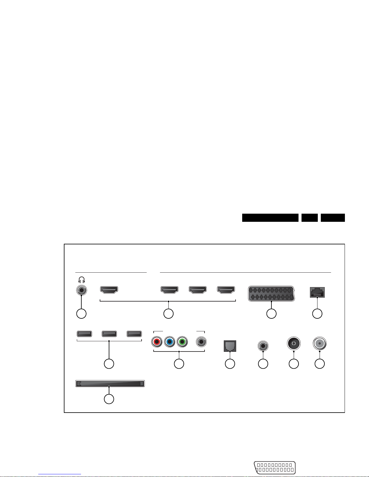
Figure 2-1 Connection overview
Note: The following connector colour abbreviations are used
(acc. to DIN/IEC 757): Bk= Black, Bu= Blue, Gn= Green, Gy=
Grey, Rd= Red, Wh= White, Ye= Yellow.
2.3.1 Connections
20 - Ground Gnd H
3 - Video RGB - In, CVBS - In/Out, Audio - In/Out
Connections
Side Rear
HDMI 4
USB USB USB
COMMON INTERFACE
HDMI 1
ARCARC ARC ARC
HDMI 2 HDMI 3 SCART
NETWORK
AUDIO OUT
ANTENNA
AUDIO IN
L / ROPTICAL
Y Pb Pr - L R
SATELLITE
19370_062_130201.eps
130404
10
5 76 8
321 4
9
11
(optional)
20
2
Page 6

Technical Specs, Diversity, and Connections
EN 6 QFU1.2E LA2.
4 - RJ45: Ethernet
Figure 2-4 Ethernet connector
1 -TD+ Transmit signal k
2 -TD- Transmit signal k
3 -RD+ Receive signal j
4 -CT Centre Tap: DC level fixation
5 -CT Centre Tap: DC level fixation
6 -RD- Receive signal j
7 -GND Gnd H
8 -GND Gnd H
5 - USB2.0
Figure 2-5 USB (type A)
1-+5V k
2 -Data (-) jk
3 -Data (+) jk
4 -Ground Gnd H
6 - Cinch: Video YPbPr - In, Audio - In
Gn - Video Y 1 V
PP
/ 75 ohm jq
Bu -Video Pb 0.7 V
PP
/ 75 ohm jq
Rd -Video Pr 0.7 V
PP
/ 75 ohm jq
Rd -Audio - R 0.5 V
RMS
/ 10 kohm jq
Wh -Audio - L 0.5 V
RMS
/ 10 kohm jq
7 - Cinch: S/PDIF - Out
Bk -Coaxial 0.4 - 0.6V
PP
/ 75 ohm kq
8 - Cinch: Audio - In (VGA/DVI)
Rd -Audio R 0.5 V
RMS
/ 10 kohm jq
Wh -Audio L 0.5 V
RMS
/ 10 kohm jq
9 - Aerial - In
- -IEC-type (EU) Coax, 75 ohm D
10 - Common Interface
68p- See Figure 10-1-35
B06I, CI conditional access jk
11 - SAT - In (optional)
- -F-type Coax, 75 ohm D
2.4 Chassis Overview
Refer to chapter 9. Block Diagrams for PWB/CBA locations.
10000_025_090121.eps
120320
1 2 3 4
10000_022_090121.eps
090121
Page 7
Precautions, Notes, and Abbreviation List
EN 7QFU1.2E LA 3.
3. Precautions, Notes, and Abbreviation List
Index of this chapter:
3.1
Safety Instructions
3.2 Warnings
3.3 Notes
3.4 Abbreviation List
3.1 Safety Instructions
Safety regulations require the following during a repair:
• Connect the set to the Mains/AC Power via an isolation
transformer (> 800 VA).
• Replace safety components, indicated by the symbol h,
only by components identical to the original ones. Any
other component substitution (other than original type) may
increase risk of fire or electrical shock hazard.
Safety regulations require that after a repair, the set must be
returned in its original condition. Pay in particular attention to
the following points:
• Route the wire trees correctly and fix them with the
mounted cable clamps.
• Check the insulation of the Mains/AC Power lead for
external damage.
• Check the strain relief of the Mains/AC Power cord for
proper function.
• Check the electrical DC resistance between the Mains/AC
Power plug and the secondary side (only for sets that have
a Mains/AC Power isolated power supply):
1. Unplug the Mains/AC Power cord and connect a wire
between the two pins of the Mains/AC Power plug.
2. Set the Mains/AC Power switch to the “on” position
(keep the Mains/AC Power cord unplugged!).
3. Measure the resistance value between the pins of the
Mains/AC Power plug and the metal shielding of the
tuner or the aerial connection on the set. The reading
should be between 4.5 M and 12 M.
4. Switch “off” the set, and remove the wire between the
two pins of the Mains/AC Power plug.
• Check the cabinet for defects, to prevent touching of any
inner parts by the customer.
3.2 Warnings
3.3.2 Schematic Notes
• All resistor values are in ohms, and the value multiplier is
often used to indicate the decimal point location (e.g. 2K2
indicates 2.2 k).
• Resistor values with no multiplier may be indicated with
either an “E” or an “R” (e.g. 220E or 220R indicates 220 ).
• All capacitor values are given in micro-farads (10
-6
),
nano-farads (n 10
-9
), or pico-farads (p 10
-12
).
• Capacitor values may also use the value multiplier as the
decimal point indication (e.g. 2p2 indicates 2.2 pF).
• An “asterisk” (*) indicates component usage varies. Refer
to the diversity tables for the correct values.
• The correct component values are listed on the Philips
Spare Parts Web Portal.
3.3.3 Spare Parts
For the latest spare part overview, consult your Philips Spare
Part web portal.
3.3.4 BGA (Ball Grid Array) ICs
Introduction
For more information on how to handle BGA devices, visit this
URL: http://www.atyourservice-magazine.com
. Select
“Magazine”, then go to “Repair downloads”. Here you will find
Information on how to deal with BGA-ICs.
BGA Temperature Profiles
For BGA-ICs, you must use the correct temperature-profile.
Where applicable and available, this profile is added to the IC
Data Sheet information section in this manual.
3.3.5 Lead-free Soldering
Due to lead-free technology some rules have to be respected
by the workshop during a repair:
• Use only lead-free soldering tin. If lead-free solder paste is
required, please contact the manufacturer of your soldering
Page 8
Precautions, Notes, and Abbreviation List
EN 8 QFU1.2E LA3.
result in sets which have the same CTN (Commercial Type
Number; e.g. 28PW9515/12) but which have a different B.O.M.
number.
By looking at the third digit of the serial number, one can
identify which B.O.M. is used for the TV set he is working with.
If the third digit of the serial number contains the number “1”
(example: AG1B033500001), then the TV set has been
manufactured according to B.O.M. number 1. If the third digit is
a “2” (example: AG2B0335000001), then the set has been
produced according to B.O.M. no. 2. This is important for
ordering the correct spare parts!
For the third digit, the numbers 1...9 and the characters A...Z
can be used, so in total: 9 plus 26= 35 different B.O.M.s can be
indicated by the third digit of the serial number.
Identification: The bottom line of a type plate gives a 14-digit
serial number. Digits 1 and 2 refer to the production centre (e.g.
SN is Lysomice, RJ is Kobierzyce), digit 3 refers to the B.O.M.
code, digit 4 refers to the Service version change code, digits 5
and 6 refer to the production year, and digits 7 and 8 refer to
production week (in example below it is 2010 week 10 / 2010
week 17). The 6 last digits contain the serial number.
6 = play 16 : 9 format, 12 = play 4 : 3
format
AARA Automatic Aspect Ratio Adaptation:
algorithm that adapts aspect ratio to
remove horizontal black bars; keeps
the original aspect ratio
ACI Automatic Channel Installation:
algorithm that installs TV channels
directly from a cable network by
means of a predefined TXT page
ADC Analogue to Digital Converter
AFC Automatic Frequency Control: control
signal used to tune to the correct
frequency
AGC Automatic Gain Control: algorithm that
controls the video input of the feature
box
AM Amplitude Modulation
AP Asia Pacific
AR Aspect Ratio: 4 by 3 or 16 by 9
ASF Auto Screen Fit: algorithm that adapts
aspect ratio to remove horizontal black
bars without discarding video
information
ATSC Advanced Television Systems
Committee, the digital TV standard in
the USA
ATV See Auto TV
Auto TV A hardware and software control
system that measures picture content,
and adapts image parameters in a
dynamic way
AV External Audio Video
AVC Audio Video Controller
AVIP Audio Video Input Processor
B/G Monochrome TV system. Sound
carrier distance is 5.5 MHz
BDS Business Display Solutions (iTV)
BLR Board-Level Repair
BTSC Broadcast Television Standard
Committee. Multiplex FM stereo sound
system, originating from the USA and
used e.g. in LATAM and AP-NTSC
countries
Page 9
Precautions, Notes, and Abbreviation List
EN 9QFU1.2E LA 3.
DNR Digital Noise Reduction: noise
reduction feature of the set
DRAM Dynamic RAM
DRM Digital Rights Management
DSP Digital Signal Processing
DST Dealer Service Tool: special remote
control designed for service
technicians
DTCP Digital Transmission Content
Protection; A protocol for protecting
digital audio/video content that is
traversing a high speed serial bus,
such as IEEE-1394
DVB-C Digital Video Broadcast - Cable
DVB-T Digital Video Broadcast - Terrestrial
DVD Digital Versatile Disc
DVI(-d) Digital Visual Interface (d= digital only)
E-DDC Enhanced Display Data Channel
(VESA standard for communication
channel and display). Using E-DDC,
the video source can read the EDID
information form the display.
EDID Extended Display Identification Data
(VESA standard)
EEPROM Electrically Erasable and
Programmable Read Only Memory
EMI Electro Magnetic Interference
EPG Electronic Program Guide
EPLD Erasable Programmable Logic Device
EU Europe
EXT EXTernal (source), entering the set by
SCART or by cinches (jacks)
FDS Full Dual Screen (same as FDW)
FDW Full Dual Window (same as FDS)
FLASH FLASH memory
FM Field Memory or Frequency
Modulation
FPGA Field-Programmable Gate Array
FTV Flat TeleVision
Gb/s Giga bits per second
G-TXT Green TeleteXT
H H_sync to the module
HD High Definition
HDD Hard Disk Drive
The SDI signal is self-synchronizing,
uses 8 bit or 10 bit data words, and has
a maximum data rate of 270 Mbit/s,
with a minimum bandwidth of 135
MHz.
iTV Institutional TeleVision; TV sets for
hotels, hospitals etc.
LS Last Status; The settings last chosen
by the customer and read and stored
in RAM or in the NVM. They are called
at start-up of the set to configure it
according to the customer's
preferences
LATAM Latin America
LCD Liquid Crystal Display
LED Light Emitting Diode
L/L' Monochrome TV system. Sound
carrier distance is 6.5 MHz. L' is Band
I, L is all bands except for Band I
LPL LG.Philips LCD (supplier)
LS Loudspeaker
LVDS Low Voltage Differential Signalling
Mbps Mega bits per second
M/N Monochrome TV system. Sound
carrier distance is 4.5 MHz
MHEG Part of a set of international standards
related to the presentation of
multimedia information, standardised
by the Multimedia and Hypermedia
Experts Group. It is commonly used as
a language to describe interactive
television services
MIPS Microprocessor without Interlocked
Pipeline-Stages; A RISC-based
microprocessor
MOP Matrix Output Processor
MOSFET Metal Oxide Silicon Field Effect
Transistor, switching device
MPEG Motion Pictures Experts Group
MPIF Multi Platform InterFace
MUTE MUTE Line
MTV Mainstream TV: TV-mode with
Consumer TV features enabled (iTV)
NC Not Connected
Page 10
Precautions, Notes, and Abbreviation List
EN 10 QFU1.2E LA3.
PDP Plasma Display Panel
PFC Power Factor Corrector (or Pre-
conditioner)
PIP Picture In Picture
PLL Phase Locked Loop. Used for e.g.
FST tuning systems. The customer
can give directly the desired frequency
POD Point Of Deployment: a removable
CAM module, implementing the CA
system for a host (e.g. a TV-set)
POR Power On Reset, signal to reset the uP
PSDL Power Supply for Direct view LED
backlight with 2D-dimming
PSL Power Supply with integrated LED
drivers
PSLS Power Supply with integrated LED
drivers with added Scanning
functionality
PTC Positive Temperature Coefficient,
non-linear resistor
PWB Printed Wiring Board (same as “PCB”)
PWM Pulse Width Modulation
QRC Quasi Resonant Converter
QTNR Quality Temporal Noise Reduction
QVCP Quality Video Composition Processor
RAM Random Access Memory
RGB Red, Green, and Blue. The primary
color signals for TV. By mixing levels
of R, G, and B, all colors (Y/C) are
reproduced.
RC Remote Control
RC5 / RC6 Signal protocol from the remote
control receiver
RESET RESET signal
ROM Read Only Memory
RSDS Reduced Swing Differential Signalling
data interface
R-TXT Red TeleteXT
SAM Service Alignment Mode
S/C Short Circuit
SCART Syndicat des Constructeurs
d'Appareils Radiorécepteurs et
Téléviseurs
SCL Serial Clock I
2
C
SWAN Spatial temporal Weighted Averaging
Noise reduction
SXGA 1280 × 1024
TFT T hin Film Transistor
THD Total Harmonic Distortion
TMDS Transmission Minimized Differential
Signalling
TS Transport Stream
TXT TeleteXT
TXT-DW Dual Window with TeleteXT
UI User Interface
uP Microprocessor
UXGA 1600 × 1200 (4:3)
V V-sync to the module
VESA Video Electronics Standards
Association
VGA 640 × 480 (4:3)
VL Variable Level out: processed audio
output toward external amplifier
VSB Vestigial Side Band; modulation
method
WYSIWYR What You See Is What You Record:
record selection that follows main
picture and sound
WXGA 1280 × 768 (15:9)
XTAL Quartz crystal
XGA 1024 × 768 (4:3)
Y Luminance signal
Y/C Luminance (Y) and Chrominance (C)
signal
YPbPr Component video. Luminance and
scaled color difference signals (B-Y
and R-Y)
YUV Component video
Page 11
Mechanical Instructions
EN 11QFU1.2E LA 4.
4. Mechanical Instructions
Index of this chapter:
4.1
Cable Dressing-
4.2 Service Positions
4.3 Assy/Panel Removal
4.4 Set Re-assembly
Notes:
• Figures below can deviate slightly from the actual situation,
due to the different set executions.
4.1 Cable Dressing-
Figure 4-1 Cable dressing 40" 8000 series
Page 12

Mechanical Instructions
EN 12 QFU1.2E LA4.
Figure 4-3 Cable dressing 42" - 47" - 55" - 60" 6000 series
19210_104_120516.eps
120516
Not available
Page 13
Mechanical Instructions
EN 13QFU1.2E LA 4.
Figure 4-5 Cable dressing 46" 8000 series
Page 14
Mechanical Instructions
EN 14 QFU1.2E LA4.
Figure 4-7 Cable dressing 46" - 55" 8000 Design series
19210_104_120516.eps
120516
Not available
Page 15

Mechanical Instructions
EN 15QFU1.2E LA 4.
Figure 4-9 Cable dressing 55" 8000 series
Page 16
Mechanical Instructions
EN 16 QFU1.2E LA4.
Figure 4-11 Cable dressing 60" 8000 series
19374_027_140110.eps
140110
Page 17

Mechanical Instructions
EN 17QFU1.2E LA 4.
Figure 4-13 Cable dressing 65" 9000 series - Back cover
19374_029_140110.eps
140110
Page 18
Mechanical Instructions
EN 18 QFU1.2E LA4.
Figure 4-15 Cable dressing 84" 9000 series - Back cover
4.2 Service Positions
For easy servicing of a TV set, the set should be put face down
on a soft flat surface, foam buffers or other specific workshop
tools. Ensure that a stable situation is created to perform
measurements and alignments. When using foam bars take
care that these always support the cabinet and never only the
display.
Caution: Failure to follow these guidelines can seriously
damage the display!
Ensure that ESD safe measures are taken.
4.3 Assy/Panel Removal
19374_031_140110.eps
140110
Page 19
Mechanical Instructions
EN 19QFU1.2E LA 4.
Figure 4-17 Rear cover removal Ambilight models -2-
4.3.2 Ambilight units in Rear Cover
The Ambilight units are affixed in the rear cover and will selfdestruct upon removal.
Attention: it is of the utmost importance to remove all remains
of any adhesive that might be left on the inside of the rear
cover.
The new units come with double-sided adhesive tape. Ensure
a correct mounting to avoid uneven light emission of the units.
4.3.3 SSB
Refer to Figure 4-18
and Figure 4-19 for details.
Some SSBs have a dedicated LVDS connector, requiring
pressing two catches as indicated in the figure, before
removing the LVDS cable.
Figure 4-19 SSB LVDS connector catches (optional) -2-
4.4 Set Re-assembly
To re-assemble the whole set, execute all processes in reverse
order.
Notes:
• While re-assembling, make sure that all cables are placed
and connected in their original position.
• Pay special attention not to damage the EMC foams in the
set. Ensure that EMC foams are mounted correctly.
19370_081_130208.eps
130208
33
19222_001_120626.eps
120626
Click!
LVDS flat foil
Click!
Page 20
Service Modes, Error Codes, and Fault Finding
EN 20 QFU1.2E LA5.
5. Service Modes, Error Codes, and Fault Finding
Index of this chapter:
5.1
Test Points
5.2 Service Modes
5.3 Start-up
5.4 Service Tools
5.5 Error Codes
5.6 The Blinking LED Procedure
5.7 Protections
5.8 Fault Finding and Repair Tips
5.9 Software Upgrading
5.1 Test Points
As most signals are digital, it will be difficult to measure
waveforms with a standard oscilloscope. However, several key
ICs are capable of generating test patterns, which can be
controlled via ComPair. In this way it is possible to determine
which part is defective.
Perform measurements under the following conditions:
• Service Default Mode.
• Video: Colour bar signal.
• Audio: 3 kHz left, 1 kHz right.
5.2 Service Modes
Service Default mode (SDM) and Service Alignment Mode
(SAM) offers several features for the service technician, while
the Customer Service Mode (CSM) is used for communication
between the call centre and the customer.
Note: For the new model range, a new remote control (RC) is
used with some renamed buttons. This has an impact on the
activation of the Service modes. For instance the old “MENU”
button is now called “HOME” (or is indicated by a “house” icon).
5.2.1 Service Default Mode (SDM)
Purpose
• To create a pre-defined setting, to get the same
measurement results as given in this manual.
• To override SW protections detected by the standby
processor and make the TV start up to the step just before
• Digital SDM: use the RC-transmitter and key in the code
“062593”, directly followed by the “MENU” (or "HOME")
button.
Note: It is possible that, together with the SDM, the main
menu will appear. To switch it “off”, push the “MENU” (or
"HOME") button again.
Figure 5-1 Service mode pad
After activating this mode, “SDM” will appear in the upper right
corner of the screen (when a picture is available).
How to Exit SDM
Use one of the following methods:
• Switch the set to STANDBY via the RC-transmitter.
• Via a standard customer RC-transmitter: key in “00”sequence.
5.2.2 Service Alignment Mode (SAM)
19370_061_130201.eps
130507
SDM
Page 21
Service Modes, Error Codes, and Fault Finding
EN 21QFU1.2E LA 5.
be re-written to NVM. The update can be done via the
NVM editor available in SAM.
• Operation hours. Displays the accumulated total of
operation hours (not the standby hours). Every time the TV
is switched “on/off”, 0.5 hours is added to this number.
• Errors (followed by maximum 10 errors). The most recent
error is displayed at the upper left (for an error explanation
see section “5.5
Error Codes”).
• Reset Error Buffer. When “cursor right” (or “OK” button)
pressed here, followed by the “OK” button, the error buffer
is reset.
• Alignments. This will activate the “ALIGNMENTS” submenu. See Chapter 6.
Alignments.
• Options numbers. Extra features for Service. For more
info regarding option codes, see chapter 6.
Alignments.
Note that if the option code numbers are changed, these
have to be confirmed with pressing the “OK” button before
the options are stored, otherwise changes will be lost.
• Initialise NVM. The moment the processor recognizes a
corrupted NVM, the “initialise NVM” line will be highlighted.
Now, two things can be done (dependent of the service
instructions at that moment):
– Save the content of the NVM via ComPair for
development analysis, before initializing. This will give
the service department an extra possibility for
diagnosis (e.g. when Development asks for this).
– Initialise the NVM.
Note: When the NVM is corrupted, or replaced, there is a high
possibility that no picture appears because the display code is
not correct. So, before initializing the NVM via the SAM, a
picture is necessary and therefore the correct display option
has to be entered. Refer to Chapter 6.
Alignments for details.
To adapt this option, it’s advised to use ComPair (the correct
values for the options can be found in Chapter 6.
Alignments)
or a method via a standard RC (described below).
Changing the display option via a standard RC: Key in the
code “062598” directly followed by the “MENU” (or "HOME")
button and “XXX” (where XXX is the 3 digit decimal display
code as mentioned on the sticker in the set). Make sure to key
in all three digits, also the leading zero’s. If the above action is
successful, the front LED will go out as an indication that the
RC sequence was correct. After the display option is changed
• Test settings. For development purposes only.
• RF4CE pairing tables. Clear paired remote control. Repairing (coldboot of platform possibly needed) can be done
by pressing the red/blue hot keys simultaneously for a few
seconds.(be sure the distance between the remote control
and TV set RF4CE receiver is less then 30cm). Message
like “Pairing successful”, confirms the match-make.
• Development 1 file versions. Not useful for Service
purposes, this information is mainly used by the
development department.
• Development 2 file versions. Not useful for Service
purposes, this information is mainly used by the
development department.
• Upload to USB. To upload several settings from the TV to
an USB stick, which is connected to the SSB. The items are
“Personal settings”, “Option codes”, “Alignments”,
“Identification data” (includes the set type and prod code +
all 12NC like SSB, display, boards), “History list”. The “All”
item supports the upload of all several items at once.
A directory “repair\” will be created in the root of the
USB stick.
To upload the settings, select each item separately, press
“cursor right” (or the “OK” button), confirm with “OK” and
wait until the message “Done” appears. In case the
download to the USB stick was not successful, “Failure” will
be displayed. In this case, check if the USB stick is
connected properly and if the directory “repair” is present in
the root of the USB stick. Now the settings are stored onto
the USB stick and can be used to download into another TV
or other SSB. Uploading is of course only possible if the
software is running and preferably a picture is available.
This method is created to be able to save the customer’s
TV settings and to store them into another SSB.
Important remark : to upload the “channel list”, select
“Home” => “Setup” => “TV settings” => “General settings”
=> “Channel list copy” => “Copy to USB”.The procedure is
also described in the (electronic) user manual.
• Download from USB. To download several settings from
the USB stick to the TV, same way of working needs to be
followed as described in “Upload to USB”. The “All” item
supports to download all several items at once.
Important remark : to download the “channel list”, select
“Home” => “Setup” => “TV settings” => “General settings”
=> “Channel list copy” => “Copy to TV”. The procedure is
Page 22
Service Modes, Error Codes, and Fault Finding
EN 22 QFU1.2E LA5.
5.2.3 Customer Service Mode (CSM)
Purpose
When a customer is having problems with his TV-set, he can
call his dealer or the Customer Helpdesk. The service
technician can then ask the customer to activate the CSM, in
order to identify the status of the set. Now, the service
technician can judge the severity of the complaint. In many
cases, he can advise the customer how to solve the problem,
or he can decide if it is necessary to visit the customer.
The CSM is a read only mode, therefore modifications in this
mode are not possible.
Provided CSM is activated, every menu from CSM can be used
as check for the back end chain video.So for all CSM content
displayed, it could be determined that the back end video chain
is working.
When CSM is activated and there is a USB stick connected to
the TV set, the software will dump the CSM content to the USB
stick.The file (CSM_model number_serial number.xml) will be
saved in the root of the USB stick. This info can be handy if no
information is displayed.
Additional in CSM mode (with USB stick connected), pressing
“OK” will create an extended CSM dump file on the USB stick.
This file (Extended_CSM_model number_serial number.xml)
contains:
• The normal CSM dump information,
• All items (from SAM “load to USB”, but in readable format),
• Operating hours,
• Error codes,
• SW/HW event logs.
To have fast feedback from the field, a flashdump can be
requested by development. When in CSM, push the “red”
button and key in serial digits ‘2679’ (same keys to form the
word ‘COPY’ with a cellphone). A file “Dump_model
number_serial number.bin” will be written on the connected
USB device. This can take 1/2 minute, depending on the
quantity of data that needs to be dumped.
Attention: for every dump which imply data tranfers to USB,
• Production code. Displays the production code (the serial
number) of the TV. Note that if an NVM is replaced or is
initialized after corruption, the production code content has
to be re-written to NVM. The update can be done via the
NVM editor available in SAM.
• Installed date. Indicates the date of the first installation of
the TV. This date is acquired by time extraction.
• Options 1. Displays the option codes numbers of option
group 1 as set in SAM (Service Alignment Mode).
• Options 2. Displays the option codes numbers of option
group 2 as set in SAM (Service Alignment Mode).
• 12NC SSB. Gives an identification of the SSB as stored in
NVM. Note that if an NVM is replaced or is initialized after
corruption, this identification number has to be re-written to
NVM. The update can be done via the NVM editor available
in SAM. This identification number is the 12nc number of
the SSB.
• 12NC display. Shows the 12NC of the display. Note that if
an NVM is replaced or is initialized after corruption, this
identification number has to be re-written to NVM. The
update can be done via the NVM editor available in SAM.
• 12NC supply. Shows the 12NC of the power supply. Note
that if an NVM is replaced or is initialized after corruption,
this identification number has to be re-written to NVM. The
update can be done via the NVM editor available in SAM.
• 12NC sensor board. Shows the 12NC of the sensor
board.
Software versions
• Current main software. Displays the build-in main
software version. In case of field problems related to
software, upgrade can be done. As this software is
consumer upgradeable, it will also be published on the
Internet.
Example: QF2xx-1.2.3.4
• Standby software. Displays the build-in standby
processor software version. Upgrading this software will be
possible via USB (see section 5.9
Software Upgrading).
Example: STDBY_77.3.11.16
• e-UM version. Displays the electronic user manual SWversion (12NC version number). Most significant number
here is the last digit.
• Strings database version. Reflects the latest embedded
Page 23
Service Modes, Error Codes, and Fault Finding
EN 23QFU1.2E LA 5.
How to Exit CSM
Press “MENU” (or "HOME") / “Back” key on the RC-transmitter.
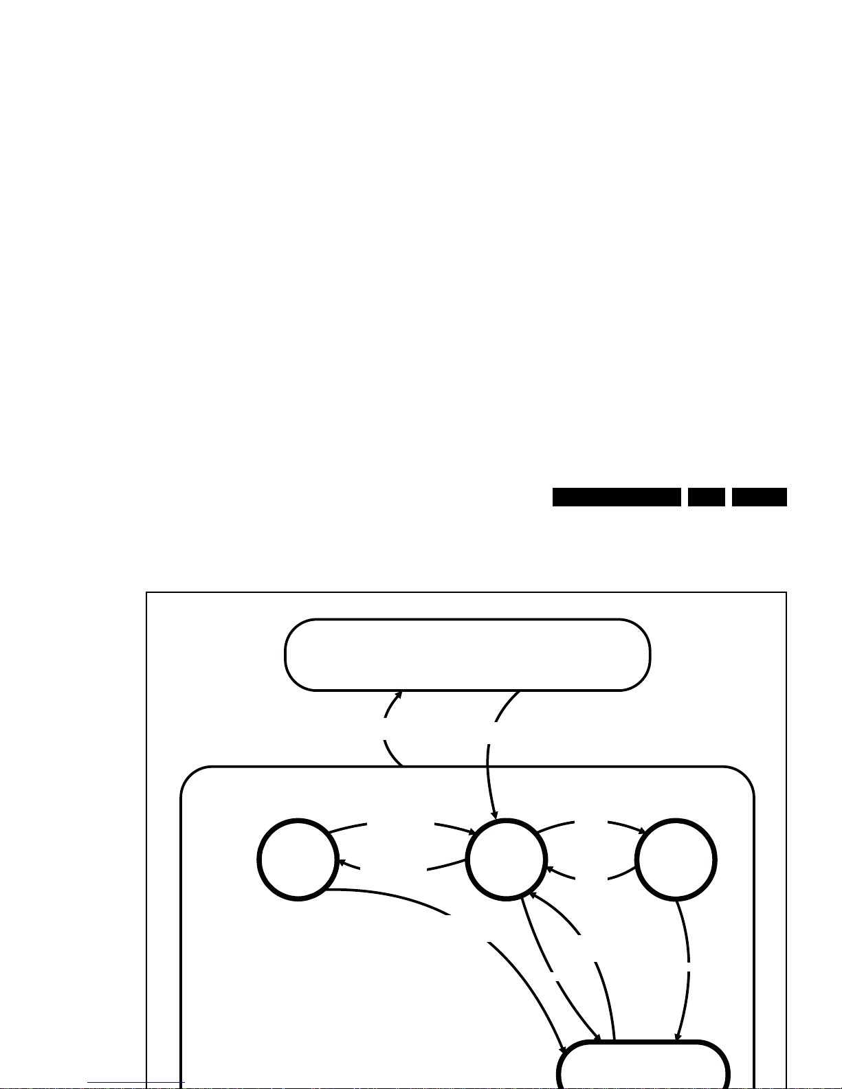
5.3 Start-up
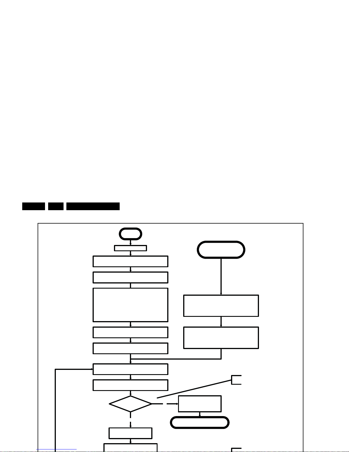
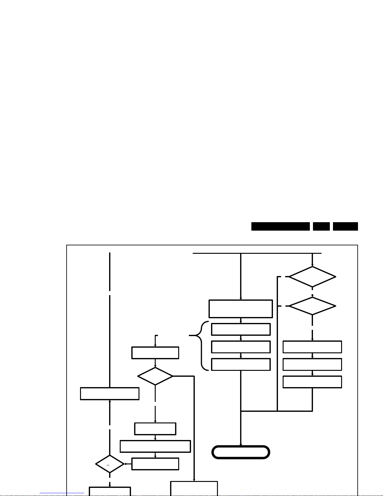
As described, the start-up diagrams below, documents which
supplies are present at any certain moment.
Active
Off
Semi
St by
St by
Mains
on
Mains
off
GoToProtection
-WakeUp requested
-Acquisition needed
- stby requested and
no data Acquisition
required
St by
requested
WakeUp
requested
Protection
WakeUp
requested
(SDM)
GoToProtection
GoToProtection
(triggered during startup
by standby µP)
Page 24
Service Modes, Error Codes, and Fault Finding
EN 24 QFU1.2E LA5.
Off
Standby Supply starts running.
All standby supply voltages become available.
st-by µP resets, resulting in a high impedant output
stage of the I/O ports.
Stand by or
Protection
AC~ Mains is applied
start keyboard scanning, RC detection.
Wake up reasons are off.
If the protection state was left by short circuiting the
SDM pins, detection of a protection condition during
startup shall stall the startup. Protection conditions
occuring in a playing set shall be ignored. The
protection mode shall not be entered.
12V platform is turned on, automatically enabling the
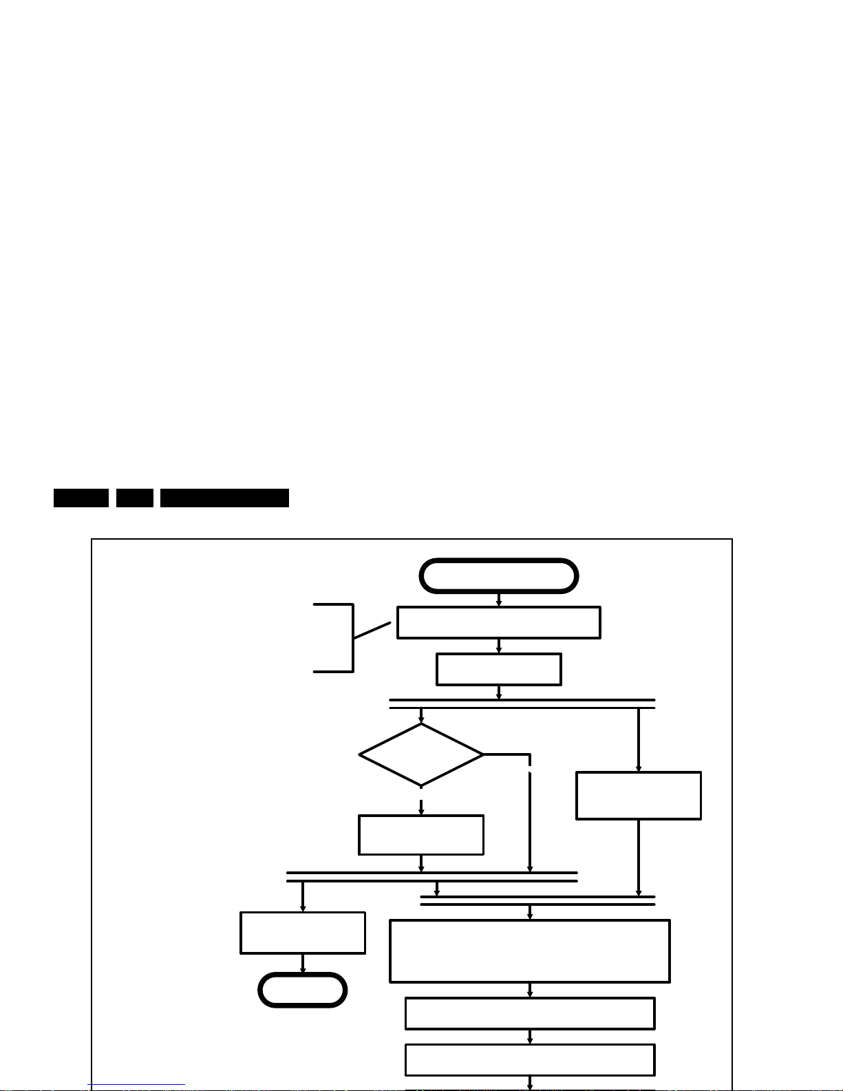
low voltage DCDC converter outputs
Enable the supply detect io n algorithm
Switch ON Platform supply by switching High the
STANDBYn line.
Initialise I/O pins of th e st-by µP
- Keep AVC syste m in reset (internal signal)
- Switch RESET-FUSION-OUTn LOW
- Switch RESET-HDMI-MUXn LOW
- Switch RESET-ETHERNETn LOW
- Switch AUDIO-MUTEn LOW
- Switch SPLASH-ON LOW
- Switch LCD-PWR-ONn High
No
Detect2 high received
within 2 seconds?
12V error:
Layer1: 3
Layer2: 16
Enter protection
Yes
Wait 300ms
All display related I/O lines should be
Switch ENABLE-WOLAN high to power Ethernet PHY
and Wifi dongle
Switch ENABLE-WOLANn high to power Ethernet
PHY and internal Wifi dongle if Networked Standby
was Off in the Standby mode.
Startup shall continue from the
moment a valid detection is received.
Page 25
Service Modes, Error Codes, and Fault Finding
EN 25QFU1.2E LA 5.
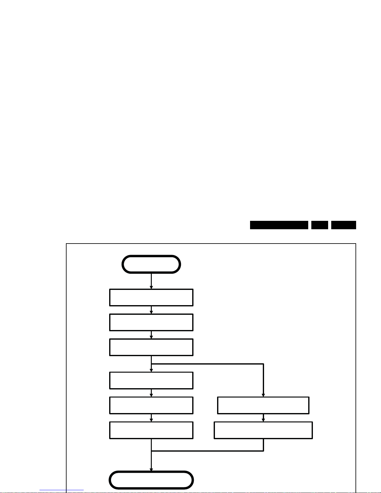
Yes
Semi-Standby
3-th try?NoSwitch Standby I/ O l ine LOW
Switch AVC in reset
Wake up reason
coldboot to Active mode?
Startup screen cfg file
present?
yes
No
No
yes
AUDIO-MUTEn is switched by MIPS code
later on in the startup process w hen audio
needs to be released
Switch RESET-FUSION-OUTn, RESET-
HDMI-MUXn , RESET-ETHE RNETn Low
Boot is failing
Reset-lines are switched
MIPS boots
Standby µP monitors
boot process and will
init a restart if Boot
process hampers
TV application starts
Set was
started with
SDM pin?
Yes
Ignore boot failure:
Stall the startup process.
Blink Layer2 error 53.
No
Wait 4 seconds before restarting
No
Blink error code
MIPS sends out startup screen
MIPS starts up the display.
Startup screen visible
Page 26
Service Modes, Error Codes, and Fault Finding
EN 26 QFU1.2E LA5.
Semi Standby
Initialize audio and video
processing IC's and functions
according needed use case.
Assert RGB video blanking
and audio mute
Wait until previous on-state is left more than2
secondsago. (to prevent LCD display problems)
The assumption here is that a fast toggle (<2s) can
only happen during ON->SEMI ->ON. In these states,
the AVC is still active and can provide the 2s delay. A
transition ON->SEMI->STB Y->SEMI->ON cannot be
made in less than 2s, because the standby state will
be maintained for at least 4s.
unblank the video
Wait until valid and stable audio and video, corresponding to the
requested output is delivered
AND
the backlight has been switched on for at least the time which is
indicated in the display file as preheat time
Release audio mute
No
Start POWER-OK line
detection algorithm as defined
in the CHS service.
return
Display already on?
(cold boot with splash
screen)
Yes
Startup display
(see separate tab)
Page 27
Service Modes, Error Codes, and Fault Finding
EN 27QFU1.2E LA 5.
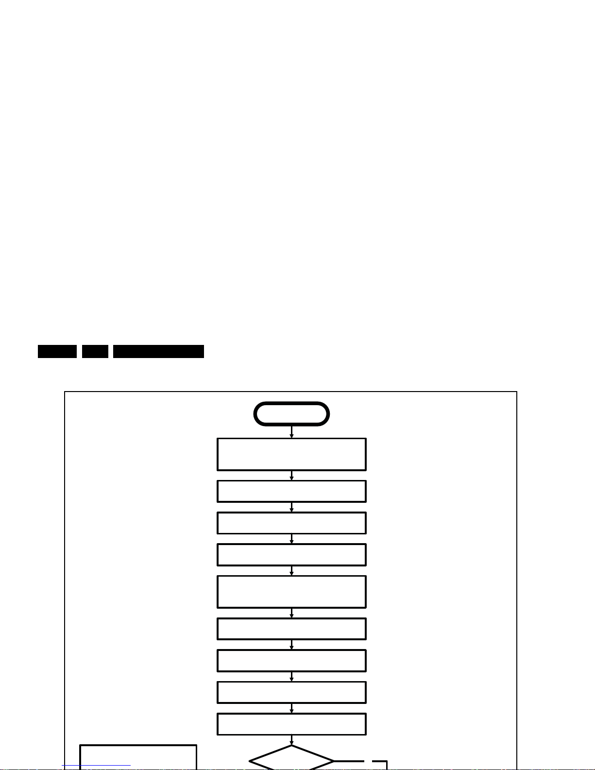
Semi Standby
Active
Mute all sound outputsaccording
information in the FMS AUDIO
Mute all video outputs switch off Ambilight (see CHS ambilight)
Wait 100ms
Wait until Ambilight has faded out:
Output power Observer should be zero
Switch off POK line detection
algorithm (see CHS service)
Shut down the display
(see separate sheet)
Switch Off LCD backlight
Page 28
Service Modes, Error Codes, and Fault Finding
EN 28 QFU1.2E LA5.
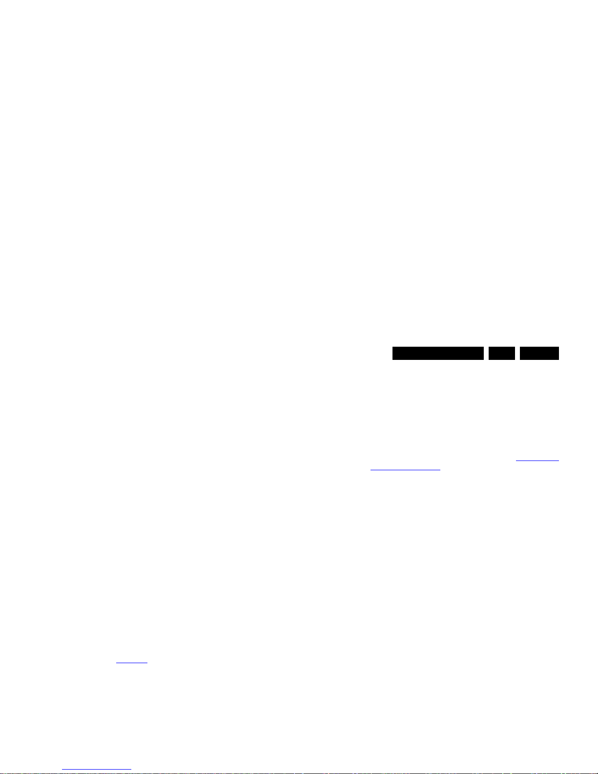
transfer Wake up reasons to the Stand by µP.
Semi Stand by
Disable all supply related protections and switch off
the DC/DC converters (ENABLE-3V3n)
No
Switch OFF all supplies by switching HIGH the
Standby I/O line
Switch AVC system in reset state
Switch reset-USB, Reset-Ethernet and Reset-DVBs
LOW
Important remarks:
release reset audio 10 sec after entering
Wait 10ms
Delay transition until ramping down of ambient light is
finished. *)
If ambientlight functionality was used in semi-standby
(lampadaire mode), switch off ambient light (see CHS
ambilight)
*) If this is not performed and the set is
switched to standby when the switch off of
the ambilights is still ongoing, the lights will
switch off abruptly when the supply is cut.
Switch RESET-FUSION-OUTn, RESET-HDMI-MUXn ,
RESET-ETHERNETn Low
Networked Standby
required?
transfer specific Firmware and Wake up reasons to the
Wifi dongle to allow networked standby
Page 29
Service Modes, Error Codes, and Fault Finding
EN 29QFU1.2E LA 5.
5.4 Service Tools
5.4.1 ComPair
The ComPair Tool is no longer supported.
5.5 Error Codes
5.5.1 Introduction
The error code buffer contains all detected errors since the last
time the buffer was erased. The buffer is written from left to
right, new errors are logged at the left side, and all other errors
shift one position to the right.
When an error occurs, it is added to the list of errors, provided
the list is not full. When an error occurs and the error buffer is
full, then the new error is not added, and the error buffer stays
intact (history is maintained).
To prevent that an occasional error stays in the list forever, the
error is removed from the list after more than 50 hrs. of
operation.
When multiple errors occur (errors occurred within a short time
span), there is a high probability that there is some relation
between them.
• If no errors are there, the LED should not blink at all in
CSM or SDM. No spacer must be displayed as well.
• There is a simple blinking LED procedure for board
level repair (home repair) so called LAYER 1 errors
next to the existing errors which are LAYER 2 errors (see
Table 5-2
).
– LAYER 1 errors are one digit errors.
– LAYER 2 errors are 2 digit errors.
• In protection mode.
– From consumer mode: LAYER 1.
– From SDM mode: LAYER 2.
• Fatal errors, if I2C bus is blocked and the set reboots,
CSM and SAM are not selectable.
– From consumer mode: LAYER 1.
– From SDM mode: LAYER 2.
• In CSM mode.
– When entering CSM: error(s) LAYER 1 will be
displayed via blinking LED.(attention: any new remote
• On screen via the SAM (only when a picture is visible).
E.g.:
– 00 00 00 00 00: No errors detected
– 23 00 00 00 00: Error code 23 is the last and only
detected error.
– 37 23 00 00 00: Error code 23 was first detected and
error code 37 is the last detected error.
– Note that no protection errors can be logged in the
error buffer.
• Via the blinking LED procedure. See section 5.5.3
How to
Clear the Error Buffer.
•Via ComPair.
5.5.3 How to Clear the Error Buffer
Use one of the following methods:
• By activation of the “RESET ERROR BUFFER” command
in the SAM menu.
• If the content of the error buffer has not changed for 50+
hours, it resets automatically.
5.5.4 Error Buffer
In case of non-intermittent faults, clear the error buffer before
starting to repair (before clearing the buffer, write down the
content, as this history can give significant information). This to
ensure that old error codes are no longer present.
If possible, check the entire contents of the error buffer. In
some situations, an error code is only the result of another error
code and not the actual cause.(e.g. a fault in the protection
detection circuitry can also lead to a protection)
There are several mechanisms of error detection:
• Via error bits in the status registers of ICs.
• Via polling on I/O pins going to the standby processor.
• Via sensing of analog values on the standby processor or
the Mips.
• Via a “not acknowledge” of an I
2
C communication.
Take notice that some errors need several minutes before they
start blinking or before they will be logged. So in case of
problems wait 2 minutes from start-up onwards, and then
check if the front LED is blinking or if an error is logged.
Page 30
Service Modes, Error Codes, and Fault Finding
EN 30 QFU1.2E LA5.
Table 5-2 Error code overview
Extra Info
• Rebooting. When a TV is constantly rebooting due to
internal problems, most of the time no errors will be logged
or blinked. This rebooting can be recognized via a ComPair
interface and Hyperterminal (for Hyperterminal settings,
see section “5.8
Fault Finding and Repair Tips, 5.8.6
Logging). It’s shown that the loggings which are generated
by the main software keep continuing.
• Error 13 (I
2
C bus M3, SSB + SRF bus blocked). Current
situation: when this error occurs, the TV can reboot due to
the blocked bus. The best way for further diagnosis here, is
to check the logging output.
• Error 14 (I
2
C bus M2, BE bus blocked). Current situation:
LAYER 2 error = 28 will be logged and displayed via the
blinking LED procedure if SDM is switched on.
• Error 31 (Lnb controller). When there is no I
2
C
communication towards this device, LAYER 2 error = 31
will be logged and displayed via the blinking LED
procedure if SDM is activated.
• Error 34 (Tuner). When there is no I
2
C communication
towards the tuner during start-up, LAYER 2 error = 34 will
be logged and displayed via the blinking LED procedure
when SDM is switched on.
• Error 35 (main NVM). When there is no I
2
C
communication towards the main NVM during start-up,
LAYER 2 error = 35 will be displayed via the blinking LED
Description Layer 1 Layer 2
Monitored
by
Error/
Prot
Error Buffer/
Blinking LED Device Defective Board
I
2
CM3 (SSB + SRF bus) 2 13 MIPS E BL / EB SSB SSB
I2CM2 (BE bus) 2 14 MIPS E BL / EB SSB SSB
I
2
CM1(FE bus) 2 18 MIPS E BL / EB SSB SSB
PNX (Fusion) doesn’t boot 2 15 Stby µP P BL Fusion SSB
12V 3 16 Stby µP P BL / Supply
HDMI mux 2 23 MIPS E EB SII9287 SSB
I2C switch 2 24 MIPS E EB PCA9540 SSB
Channel dec DVB-T2 2 27 MIPS E EB CXD2834 SSB
Channel dec DVB-S2 2 28 MIPS E EB SI2169 SSB
Lnb controller 2 31 MIPS E EB LNBH25 SSB
Hybrid Tuner 2 34 MIPS E EB SUT-RE214Z SSB
Main NVM 2 35 MIPS E EB M24C64 SSB
Tuner DVB-S2 2 36 MIPS E EB STV611X SSB
Class-D 2 37 MIPS E EB TAS 5731 PHP SSB
µProcessor PQ 2 38 MIPS E EB LPC1114 SSB
IO Expander 2 41 MIPS E EB PCA9554 SSB
T° sensor SSB/set 2 42 MIPS E EB LM75 T° sensor/SSB
Light sensor 6 43 MIPS E EB TSL2571 Set
µP touch control 6 44 MI PS E EB / Set
RF4CE 6 46 MIPS E EB / Set
MIPS doesn’t boot (SW cause) 2 53 Stby µP P BL FUSION SSB
NT72314 9 61 MIPS E EB NT72314/ QFHD
NT68361 9 62 MIPS E EB NT68361/ QFHD
NT72314 not alive 9 63 MIPS E EB NT72314/ QFHD
NT68361 not alive 9 64 MIPS E EB NT68361/ QFHD
Page 31

Service Modes, Error Codes, and Fault Finding
EN 31QFU1.2E LA 5.
displayed via the blinking LED procedure when SDM is
switched “on”.
• Error 46 (RF4CE). When there is no I
2
C communication
towards the RF4CE driver during start-up, LAYER 2
error = 46 will be logged and displayed via the blinking LED
procedure when SDM is switched “on”.
• Error 53. This error will indicate that the Fusion device has
read his bootscript (when this would have failed, error 15
would blink) but initialization was never completed because
of hardware problems (NAND flash, DDR...) or software
initialization problems. Possible cause could be that there
is no valid software loaded (try to upgrade to the latest main
software version). Note that it can take a few minutes
before the TV starts blinking LAYER 1 error = 2 or in SDM
(maintain grounding continuously), LAYER 2 error = 53.
• Error 61 (NT72314). When there is no I
2
C acknowledge
from the Novatek device (Quad full HD Bolt-on board)
towards the MIPS during start-up, LAYER 2 error = 61 will
be logged.Here, the Novatek device operates as frame rate
convertor.
• Error 62 (NT68361). When there is no I
2
C acknowledge
from the Novatek device (Quad full HD Bolt-on board)
towards the MIPS during start-up, LAYER 2 error = 62 will
be logged.Here, the Novatek device supports the 4K HDMI
to LVDS conversion.
• Error 63 (NT72314 not alive).Error generated via I
2
C by
the device itself, although acknowledge passed and
confirmed.
• Error 64 (NT68361 not alive).Error generated via I
2
C by
the device itself, although acknowledge passed and
confirmed.
5.6 The Blinking LED Procedure
5.6.1 Introduction
The blinking LED procedure can be split up into two situations:
• Blinking LED procedure LAYER 1 error. In this case the
error is automatically blinked when the TV is put in CSM.
This will be only one digit error, namely the one that is
referring to the defective board (see table “5-2
Error code
overview”) which causes the failure of the TV. This
approach will especially be used for home repair and call
5. One long blink of 3 s to finish the sequence (spacer).
6. The sequence starts again.
5.6.2 How to Activate
Use one of the following methods:
• Activate the CSM. The blinking front LED will show the
layer 1 error(s), this works in “normal operation” mode or
automatically when the error/protection is monitored by the
standby processor.
In case no picture is shown and there is no LED blinking,
read the logging to detect whether “error devices” are
mentioned. (see section “5.8
Fault Finding and Repair
Tips, 5.8.6 Logging”).
• Activate the SDM. The blinking front LED will show the
entire content of the LAYER 2 error buffer, this works in
“normal operation” mode or when SDM (via hardware pins)
is activated when the tv set is in protection.
5.7 Protections
5.7.1 Software Protections
Most of the protections and errors use either the standby
microprocessor or the MIPS controller as detection device.
Since in these cases, checking of observers, polling of ADCs,
and filtering of input values are all heavily software based,
these protections are referred to as software protections.
There are several types of software related protections, solving
a variety of fault conditions:
• Related to supplies: presence of the +5V, +3V3, +2V5,
+1V2 and +1V1 needs to be measured, no protection
triggered here.
• Protections related to breakdown of the safety check
mechanism. E.g. since the protection detections are done
by means of software, failing of the software will have to
initiate a protection mode since safety cannot be
guaranteed any more.
Remark on the Supply Errors
The detection of a supply dip or supply loss during the normal
playing of the set does not lead to a protection, but to a cold
Page 32
Service Modes, Error Codes, and Fault Finding
EN 32 QFU1.2E LA5.
5.8.2 CSM
When CSM is activated and there is a USB stick connected to
the TV, the software will dump the complete CSM content to the
USB stick. The file (Csm.xml) will be saved in the root of the
USB stick. If this mechanism works it can be concluded that a
large part of the operating system is already working (MIPS,
USB...)
5.8.3 Power conversion and distribution.
Description
Input power for the TV platform comes from the main power
supply that delivers +3V5-STANDBY (pin 9 of connector 1M90)
and +12V (pins 11,12 and 25,26 of the same connector). +3V5STANDBY (3.5V nominal) is the permanent voltage while +12V
is started by the STANDBY signal (connector 1M90, pin 10)
when going from high to low. +12V is split in few branches via
fuses 1UA0 (+12Va), 1UA1 (+12Vb) and 1UP1(+12-DVBS):
• +12Va serves as input voltage for the switching voltage
regulators that deliver +1V1-FD and +1V5.
• +12Vb is used as input voltage for the switching voltage
regulators that deliver +3V3 and +5V.
• +12V-DVBS (if DVB-S functionality is present) goes to 12V
and +V-LNB switching regulators.
The on board power supply consists of 4 switching voltage
regulators (5 in case of DVB-S version), 8 linear voltage
regulators (9 in case of DVB-S version) and an over-current
protection circuit for 12V (AMBI-POWER) ambilight boards.
All switching voltage regulators have 12V input voltage and
deliver:
• +1V1-FD Fusion main core supply voltage (0.95V...1.2V depending on DVS1 signal), stabilized close to the point of
load by means of SENSE+1V1-FD signal.
• +1V5 supply voltage (1.53V nominal), for the DDR3
memories and DDR3 interface of the Fusion chip and +1V5
to +1V2-MIPS and +1V5 to +1V2-FE linear voltage
regulators.
• +3V3 supply voltage (3.32V nominal): overall 3.3V for on
board IC’s and external ambientlight panels, also used as
Start-up of switching converters is triggered by DETECT12V
signal that becomes high when +12V rises above 10V and
stays above 9V (1V hysteresis).DETECT12V is used as enable
signal by the +12V to +5V switching converter;+12V to +1V1FD and +12V to +1V5(and +1V2-MIPS) will start at the same
time with +5V due to ENABLE+1V5+1V1 that is set high by
DETECT12V signal.Tuners are supplied from their respective
linear voltage regulators when +5V starts.The rest of the supply
voltages (+3V3, +2V5, +1V2-FA, +1V2-FE and +1V1-FA) are
switched on a few milliseconds later by signal ENABLE+3V3.
In case of TV sets having ambilight consumption from +12V
higher than 1A, the electronic protection circuit (7UAC or 7UAD
and surrounding components) is used instead of fuse 1UA2.
AMBI-POWER should be available shortly (100 ms) after +12V
starts if there is no load on it. The over-current trigger level is
around 4.1A for 7UAC and 3.5A for 7UAD. Once the overcurre
nt protection is triggered, it can be reset by removing the
shortcircuit cause and keeping it under no load condition for
about 100 ms.
Important remark: for tests, GND-AL must be connected to
platform GND.
+V-LNB value is set via the I
2
C bus: around 13V for vertical
polarized satellite channels and around 18V for the horizontal
ones. Maximum output current is limited to 400mA
Debugging
The best way to find a failure in the DC/DC converters is to
check their start-up sequence at power “on”, presuming that
the external supply is operational. Take the STANDBY signal
"high"-to-"low" transition as trigger reference and check the
power start-up sequence as described above.
Tips
• Behaviour comparison with a working Fusion R3 platform
can be a fast way to locate failures.
• Check first the integrity of fuses 1UA0, 1UA1 and (if
present) 1UA2 and 1UP1.
• If a fuse is found interrupted: check the respective +12Va
(or +12Vb or +12V-DVBS) short circuit with all of the
derived supply voltages, for example: a +12Va ->+1V5
Page 33
Service Modes, Error Codes, and Fault Finding
EN 33QFU1.2E LA 5.
in Hyperterminal. The Hyperterminal is available in every
Windows application via Programs, Accessories,
Communications, Hyperterminal. Connect a “ComPair UART”cable (3138 188 75051) from the service connector in the TV to
the “multi function” jack at the front of ComPair II box.
Required settings in ComPair before starting to log:
- Start up the ComPair application.
- Select the correct database (open file “QFUX.X”, this will set
the ComPair interface in the appropriate mode).
- Close ComPair
After start-up of the Hyperterminal, fill in a name (f.i. “logging”)
in the “Connection Description” box, then apply the following
settings:
1. COMx
2. Bits per second = 115200
3. Data bits = 8
4. Parity = none
5. Stop bits = 1
6. Flow control = none
During the start-up of the TV set, the logging will be displayed.
This is also the case during rebooting of the TV set (the same
logging appears over and over). Also available in the logging is
the “Display Option Code” (useful when there is no picture),
look for item “display number xxx” in the beginning of the
logging. Tip: when there is no picture available during rebooting
you are able to check for “error devices” in the logging (LAYER
2 error) which can be very helpful to determine the failure cause
of the reboot. For protection state, there is no logging.
5.8.7 Guidelines Uart logging
Description possible cases:
Uart loggings are displayed:
• When Uart loggings are coming out, the first conclusion we
can make is that the TV set is starting up and
communication with the flash RAM seems to be supported.
The Fusion processor is able to read and write in the
DRAMs.
• We can not yet conclude: Flash RAM and DRAMs are fully
operational/reliable.There still can be errors in the data
transfers, DRAM errors, read/write speed and timing
control.
Startup in Jett Mode:
Check Uart logging in Jet mode mentioned as : “JETT UART
READY”.
5.8.8 Memory test
The memory test is running in the background of the main
TV software.It allocates a memory pool used to write and
read back predefined data, as reference to detect possible
memory corruption.The memory test is enabled by dial-in
of sequence “6636” while the remote control (dedicated) is
in DVD mode and the TV in CSM.Once the red LED in the
front of the TV set starts blinking, exit CSM in order to
display video.As long as the memory test is running and
no error is detected, the standby LED is blinking.Upon
detection of errors, the standby LED stays continuous ON
and details will be shown in the prints of the Uart logging.It
is not possible to stop the memory test once launched
unless the TV is restarted, also increase/decrease the
frequency of the memory interface can not be set.
Startup procedure:
• Switch ON the TV set.
• Set TV use case (preferably DVBT H264 or HDMI1080p).
• Invoke CSM (dial-in “123654”on the remote control).
• Set the remote control in DVD mode, and enter sequence
“6636”.
• Check the loggings coming from the service connector
(Mips Uart prints) :
“**MemoryTest No errors found so far (loop xx)”
xx : number of tests done.
• As long as the memory test is running and no error is
detected, the standby LED is blinking continuously, upon
detection of errors, the standby LED stays ON.
• Get out of CSM in order to see video.
COM port settings:
• Baud rate: 115200
• Data: 8 bits
• Parity: none
• Stop: 1 bit
• Flow control: none
Page 34
Service Modes, Error Codes, and Fault Finding
EN 34 QFU1.2E LA5.
5.8.10 Power Supply
In case of no picture when CSM (test pattern) is activated and
backlight doesn’t light up, it’s recommended first to check the
LED drivers on the PSL(S).
Attention point for cable handling: (dis)connection for power
cable (power supply <=> SSB) should always be executed
without any bending or mechanical stress on the outisdes of
the connector 1M90.Risk of double pins inside the connector
should be avoid in this way.
5.8.11 Display option code
Attention: In case the SSB is replaced, always check the
display option code number (group 2, first option number e.g.
“44855”) in SAM, even when picture is available. Performance
with the incorrect display option code can lead to unwanted
side-effects for certain conditions.
Also supported in this chassis:
The display option code can be changed by “062598 HOME
XXX” special SAM command (XXX=display option in 3 digits).
Page 35
Service Modes, Error Codes, and Fault Finding
EN 35QFU1.2E LA 5.
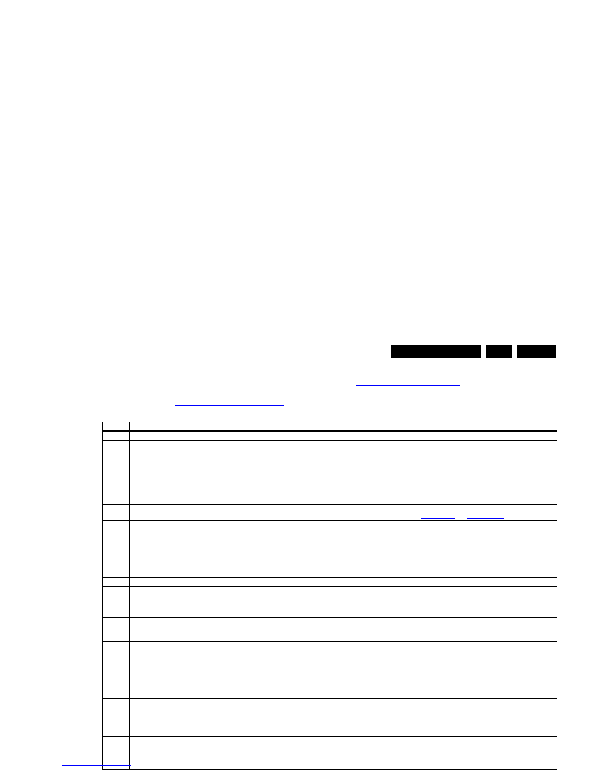
5.8.12 SSB Replacement
Follow the instructions in the flowchart in case a SSB has to be
exchanged. See table 5-3
SSB replacement instructions.
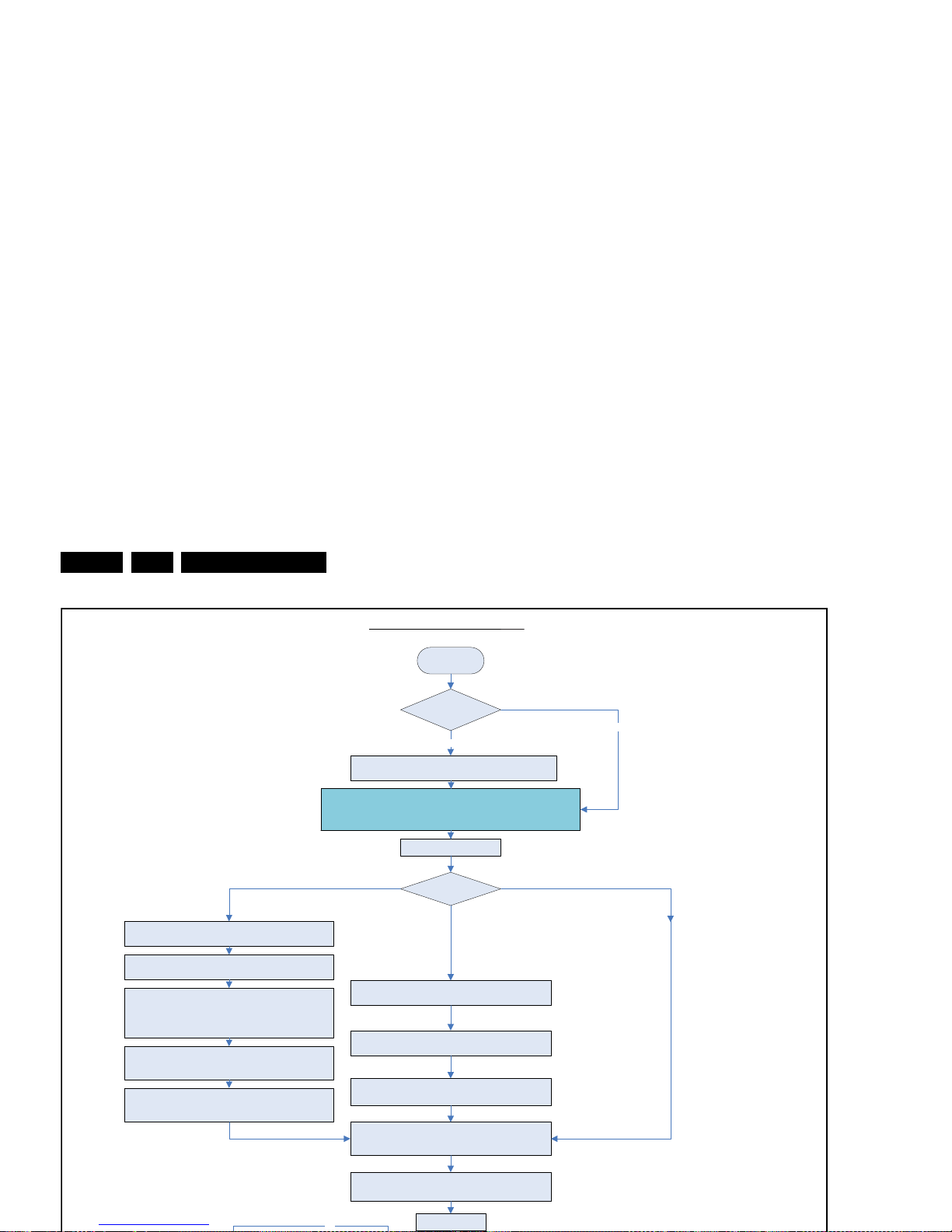
For a more general overview of steps to follow, refer to figure
5-11
SSB replacement flowchart.
Table 5-3 SSB replacement instructions
Step # Action to do Advise / Attention points / Remarks
1 Ensure ESD protection by using a wristband 2 If SSB is still functional: Go via SAM to “upload to USB” and copy Personal
settings - Option codes - Alignments (Presets) - Set Identification.
Advice: because of differences in memory al location, it is adv ised to up grade
main SW before copying data from existing SSB. Copy of Preset list is
possible from normal user interface.
Upload to USB: a directory “repair” will be created on the USB, and all data will be copied in this
directory. In case of issues by copying the program map table, it is advised to reinstall the
programs from Virgin mode instead of using copy via USB.
3 Disconnect set from mains and from antenna. Safety and ESD!
4 Open the set and disconnect LVDS flat cable. Disconnect other cables /
connections.
Always take care for ESD! Be extra careful when removing connectors!
5 Dismount the (defective) SSB from the set. Do not damage SSB copper tracks with your tools! Do not scratch bottom of SSB (be very car eful
by moving SSB over SSB supports). See Figure 5-9 and Figure 5-10.
6 Place new SSB in the set, and fixate/mount carefully. D o not damage SSB copper tracks with your tools! Do not scratch bottom of SSB (be very ca reful
by moving SSB over SSB supports). See Figure 5-9 and Figure 5-10.
7 Connect PSU and other connectors. Insert the optional WiFi module. Make sure that the connectors are correctly plugged-in and locked (click). Special attention for the
optional WiFi module: a defective WiFi module can give re boots or no start- up of the SSB . In this
case do a trial without WiFi module.
8 Connect LVDS connector(s). Be very careful: wrong or bad connection can damage the TCON part on the SSB and damage
the LCD display. Check if flat cables are fitted correctly before closing the connector lock.
9 Connect set to mains and switch TV “On”. Check start-up of the set, backlight switching “On”.
10 If the set does not start (or reboots) check:
- The connectors from the power supply,
- The power supply cable and connec tion pins,
- LVDS cable connection.
Power supply connector must “snap” into the socket.
11 Before programming the new SSB, upgrade to latest software. If set is starting
up in software upgrade mode, then first install new software via software
Upgrade Menu or via the autorun.upg file.
Some SSB’s will start-up in software upgrade mode, and software needs to be installed before you
can program the Display Option codes. It’s adviced to use an autorun.upg file for software
upgrade, this in case you have no OSD on the screen.
12 If set is starting up without picture or menu (OSD), first program the correct
Display Option codes.
Use blind service mode “062598” + “Home” button, directly followed by the
Display Option code (3 digits). Set will switch to Standby after Display Option code is entered.
13 Go to SAM and program “Set type” and “Serial number”. This is possible via
the NVM editor and virtual keyboard. In case personal settings were
recovered from the defective SSB, you can use an “Upload from USB”.
Programming “Set type” and “Serial number” is mandatory to have all functionality of the set, like
DLNA, Net TV… For certain sets you may need to use ComPair for this.
14 Check if option codes are correct, and keys are present. SSBs w ith integrated
TCON needs TCON alignment in SAM.
Validity of HDCP, CI+, Marlin, and WDRM keys can be checked via ComPair.
15 Update to latest software (Standby and main software). This step is necessary
to make sure that the (optional) 200Hz T-CON board has the latest software.
Even when the SSB already has the latest softwar e, it is manda tory to upgrade a gain the softwar e
to update the 200 Hz T-CON part. At the end of the main software update process, a dedicated
software is loaded, from the main processor via the LVDS connection, to upgrade the
200 Hz T-CON part. For certain LCD displays, a dedicated Display software patch (autoscript) is
available. See General Service info GSC_85590.
16 Once the set is playing, check cable connection between PSU and SSB, by
moving the cable if there are no bad connections.
Check the two power connectors on 1M90. Bad co ntact or ba d connectio n here can give rebo ots.
17 Fill in the Electronic DDF (Defect Description Form): Fault symptom, TV type
and TV serial number.
It is mandatory to fill in the E-DDF form (see the “At Your Service” web portal).
Page 36
Service Modes, Error Codes, and Fault Finding
EN 36 QFU1.2E LA5.
START
C onne c t the U SB stic k to the set,
go to SAM and save the current TV settings via “Upload to USB”
Set is stil l operatin g?
Yes
1.
Dismount the defective SSB.
2. Replace the SSB by a Service SSB.
Set behaviour?
No
No
Instruction note SSB replacement Q55x.x
Before starting:
- prepare a USB memory stick with the latest software
- download the latest Main Software (Fus) from www.p4c.philips.com
- unzip this file
- create a folder ”upgrades” in the root of a USB stick (size > 50 MB) and
save the autorun.upg file in this "upgrades" folder.
Note: it is possible to rename this file, e.g."Q54x_SW_version.upg"; this in
case there are more than one "autorun.upg" files on the USB stick.
No picture displayed
Picture displayed
Set is starting up without software
upgrade menu appearing on screen
Picture displayed
Set is starting up with software
upgrade menu appearing on screen
Due to a possible wrong display option code in the received Service
SSB (NVM), it’s possible that no picture is displayed. Due to this
the download application will not be shown either. This tree enables you
to load the main software step-by-step via the UART logging on the PC
(this for visual feedback).
Start-up the set
1) Start up the TV set, equiped with the Service SSB,
and enable the U
ART logging on the PC.
2) The TV set will start-up automatically in the
download application if main TV software is not loaded.
3) Plug the prepared USB stick into the TV set. Follow the
instructions in the UART log file, press “Right” cursor key to enter
the list. Navigate to the “autorun.upg” file in the UART logging
printout via the cursor keys on the remote control. When the
correct file is selected, press “Ok”.
4) Press "Do
wn" cursor and “Ok” to start flashing the main
TV software. Printouts like: “L: 1-100%, V: 1-100% and
P: 1-100%” should be visible now in the UART logging.
5) Wait until the message “Operation successful !” is logged in
the UART log and remove all inserted media. Restart the TV set.
1) Plug the USB stick into the TV set and select
the “autorun .upg” file in the display
ed browser.
2) Now the main software will be loaded automatically,
supported by a progress bar.
3) Wait until the message “Operation successful !” is displayed
and remove all inserted media. Restart the TV set.
Set the correct “Display code” via “062598 -HOME- xxx” where
“xxx” is the 3 digit display panel code (see stic
ker on the side
or bottom of the cabinet)
After entering the “Display Option” code, the set is going to
Standby
(= validation of code)
Restart the set
Page 37
Service Modes, Error Codes, and Fault Finding
EN 37QFU1.2E LA 5.
Set is startin g up in Factory mode
Set is starting up in Factor y mod e?
Noisy picture with bands/lines is visible and the
RED LED is continuous on.
An “F” is displayed (and the HDMI 1
input is displayed).
- Press the “volume minus” button on the TVs local keyboard for 5 ~10
seconds
- Press the “SOURCE” button for 10 seconds until the “F” disappears
from the screen or the noise on the screen is replaced by “blue mute”
The noise on the screen is replaced
with the blue mute or the “F” is disappeared!
Unplug the mains cord to verify the correct
disabling of the Factory mode.
Page 38
Service Modes, Error Codes, and Fault Finding
EN 38 QFU1.2E LA5.
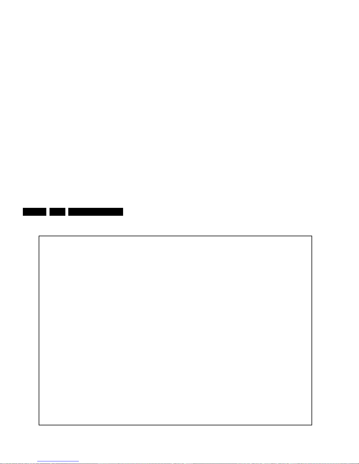
Figure 5-13 SSB start-up
5.9 Software Upgrading
Automatic Software Upgrade
In “normal” conditions, so when there is no major problem with
18753_211_100811.eps
110810
Page 39
Service Modes, Error Codes, and Fault Finding
EN 39QFU1.2E LA 5.
1. Create a directory “UPGRADES” on the USB stick.
2. Rename the “autorun.upg” to something else, e.g. to
“software.upg”. Do not use long or complicated names,
keep it simple. Make sure that “AUTORUN.UPG” is no
longer present in the root of the USB stick.
3. Copy the renamed “upg” file into this directory.
4. Insert USB stick into the TV.
5. The renamed “upg” file will be visible and selectable in the
upgrade application.
Back-up Software Upgrade Application
If the default software upgrade application does not start (could
be due to a corrupted boot sector) via the above described
method, try activating the “back-up software upgrade
application”.
How to start the “back-up software upgrade application”
manually:
1. Disconnect the TV from the Mains/AC Power.
2. Press the “CURSOR DOWN”-button on a Philips TV
remote control while reconnecting the TV to the Mains/AC
Power.(attention : not supported by use of RF4CE remote
due to the fact this application is not running yet at the time
of the “CURSOR-DOWN” request).
3. The back-up software upgrade application will start.
5.9.3 Standby Software Upgrade via USB
In this chassis it is possible to upgrade the Standby software
via a USB stick. The method is similar as upgrading the main
software via USB.
Use the following steps:
1. Create a directory “UPGRADES” on the USB stick.
2. Copy the Standby software (one-zip file StandbyUpgrade,
e.g. StandbyFactory_77.03.12.00_16.00.00.upg) into this
directory.
3. Insert the USB stick into the TV.
4. Start the download application manually (see section “
Manual Software Upgrade”.
5. Select the appropriate file and press the “OK” button to
upgrade.
5.9.4 Content and Usage of the One-Zip Software File
Page 40
Alignments
EN 40 QFU1.2E LA6.
6. Alignments
Index of this chapter:
6.1
General Alignment Conditions
6.2 Hardware Alignments
6.3 Software Alignments
6.4 Option Settings
6.5 Reset of Repaired SSB
6.6 Total Overview SAM modes
6.1 General Alignment Conditions
Perform all electrical adjustments under the following
conditions:
• Power supply voltage (depends on region):
– AP-NTSC: 120 VAC or 230 V
AC
/ 50 Hz ( 10%).
– AP-PAL-multi: 120 - 230 V
AC
/ 50 Hz ( 10%).
– EU: 230 V
AC
/ 50 Hz ( 10%).
– US: 120 V
AC
/ 60 Hz ( 10%).
– LATAM-NTSC: 120 - 230 V
AC
/ 50 Hz ( 10%).
• Connect the set to the mains via an isolation transformer
with low internal resistance.
• Allow the set to warm up for approximately 15 minutes.
• Measure voltages and waveforms in relation to correct
ground (e.g. measure audio signals in relation to
AUDIO_GND). Caution: It is not allowed to use heat sinks
as ground.
• Test probe: Ri > 10 M, Ci < 20 pF.
• Use an isolated trimmer/screwdriver to perform
alignments.
6.1.1 Alignment Sequence
• First, set the correct options:
– In SAM, select “Option numbers”.
– Fill in the option settings for “Group 1” and “Group 2”
according to the set sticker (see also paragraph 6.4
Option Settings).
– Press OK on the remote control before the cursor is
moved to the left.
– In submenu “Option numbers” select “Store” and press
OK on the RC.
•OR:
– In main menu, select “Store” again and press OK on
• LATAM models: an NTSC M TV-signal with a signal
strength of at least 1 mV and a frequency of 61.25 MHz
(channel 3).
6.3.1 White Point
• Choose “Home”, “Setup”, “TV Settings” and then “Picture”
and set picture settings as follows:
• In menu “Picture”, choose “Pixel Precise HD” and set
picture settings as follows:
• Go to the SAM and select “Alignments”-> “White point”.
White point alignment LCD screens:
• Use a 100% white screen (format: 720p50) to the HDMI
input and set the following values:
– “Colour temperature”: “Cool”.
– All “White point” values to: “127”.
In case you have a colour analyser:
• Measure, in a dark environment, with a calibrated
contactless color analyser (e.g.Minolta CA-210) in the
centre of the screen and note the x, y value.
• Apply a 90% full white screen to the HDMI input and select
this input.Format : 720p50.If a Quantum Data generator is
used, it’s recommended to select the “FLAT” predefined
setting from the device.
• Adjust the correct x, y coordinates (while holding one of the
White point registers R, G or B on 127) by means of
Picture Setting
Contrast 100
Brightness 50
Colour 0
Light Sensor Off
Picture format Unscaled
Picture Setting
Dynamic Contrast Off
Dynamic Backlight Off
Colour Enhancement Off
Gamma (advanced) 0
Page 41
Alignments
EN 41QFU1.2E LA 6.
• Select a COLOUR TEMPERATURE (e.g. COOL,
NORMAL, or WARM).
• Set the RED, GREEN and BLUE default values according
to the values in Table 6-5
.
• When finished press OK on the RC, then press STORE (in
the SAM root menu) to store the aligned values to the NVM.
• Restore the initial picture settings after the alignments.
Table 6-3 White tone default settings 40" PFL series
Table 6-4 White tone default settings 42" PFL series
Table 6-5 White tone default settings 46" PFL series
Table 6-6 White tone default settings 46" PDL series
Table 6-7 White tone default settings 47" PFL series
Table 6-9 White tone default settings 55" PDL series
Table 6-10 White tone default settings 60" PFL series
Table 6-11 White tone default settings 65" PFL series
Table 6-12 White tone default settings 84" PFL series
White Tone 40PFL8008/x
Colour Temp R G B
Normal 127 110 110
Cool 123 115 127
Warm 127 99 72
White Tone 42PFLxxx8/x
Colour Temp R G B
Normal 127 118 116
Cool 120 120 127
Warm 127 108 74
White Tone 46PFL8008/x
Colour Temp R G B
Normal 127 99 108
Cool 124 102 125
Warm 127 87 71
White Tone 46PDL8908/x
Colour Temp R G B
Normal 127 92 92
Cool 127 98 110
Warm 127 84 58
White Tone 55PFL8008/x
Colour Temp R G B
Normal 127 103 113
Cool 122 103 127
Warm 127 90 74
White Tone 55PDL8908/x
Colour Temp R G B
Normal 127 96 98
Cool 127 100 116
Warm 127 88 59
White Tone 60PFL6008/x
Colour Temp R G B
Normal 127 108 103
Cool 127 115 121
Warm 127 96 63
White Tone 60PFL8708/x
Colour Temp R G B
Normal 127 123 91
Cool 124 125 111
Warm 127 118 51
White Tone 65PFL9708/x
Colour Temp R G B
Normal 125 123 125
Cool 113 115 127
Warm 127 113 89
White Tone 84PFL9708/x
Colour Temp R G B
Normal 127 112 118
Page 42
Alignments
EN 42 QFU1.2E LA6.
Table 6-13 Overview matrix correction table
6.4 Option Settings
6.4.1 Introduction
The microprocessor communicates with a large number of I
2
C
ICs in the set. To ensure good communication and to make
digital diagnosis possible, the microprocessor has to know
which ICs to address.
Notes:
• After changing the option number(s), save them by
pressing the “OK” button on the RC before the cursor is
moved to the left, select “STORE” in the SAM root menu
and press “OK” on the RC.
• The new option setting is only active after the TV is
switched “off” / “standby” and “on” again with the mains
switch (the NVM is then read again).
6.4.2 (Service) Options
From 2011 onwards, it is not longer possible to change
individual option settings in SAM. Options can only be changed
all at once by using the option codes as described in section
6.4.4
.
6.4.3 Option Code Overview
Refer to the rearcover sticker in the set for the correct option
Diversity
Not all sets with the same Commercial Type Number (CTN)
necessarily have the same option code!
Use of Alternative BOM => an alternative BOM number usually
indicates the use of an alternative display or power supply. This
results in another display code thus in another Option code.
Refer to Chapter 2.
Technical Specs, Diversity, and
Connections.
6.5 Reset of Repaired SSB
A very important issue towards a repaired SSB from a Service
repair shop (SSB repair on component level) implies the reset
of the NVM on the SSB.
A repaired SSB in Service should get the service Set type
“00PF0000000000” and Production code “00000000000000”.
Also the virgin bit needs to be set. To set all this, you can use
the ComPair tool or use the “NVM editor” and “Setup => TV
settings => General settings => Reinstall TV” (virgin mode).
After a repaired SSB has been mounted in the set (set repair
on board level), the type number (CTN) and production code +
12NC’s (SSB, display and supply) of the TV has to be set
according the type plate of the set (no info on 12NC’s here). For
this, you can use the NVM editor in SAM. This action also
ensures the correct functioning of the “Smart TV” feature and
access to the Smart TV portals. The loading of the CTN and
production code can also be done via ComPair (Model number
programming).
After a SSB repair, the original channel map can be restored,
provided that the original channel map was stored on a USB
stick before repair was commenced and that basic functionality
of the TV, needed for this procedure, was not hampered as a
result of the defect. The procedure of “channel map cloning” is
clearly described in the (electronic) user manual.
Matrix # fR fG fB
Matrix 0 1 1 1
Matrix 1 1 0.9 0.9
Matrix 2 0.9 1 0.9
Matrix 3 0.9 0.9 1
Matrix 4 0.9 1 1
Matrix 5 1 0.9 1
Matrix 6 1 1 0.9
Matrix 7 0.95 1 1
Matrix 8 1 0.95 1
Matrix 9 1 1 0.95
Page 43
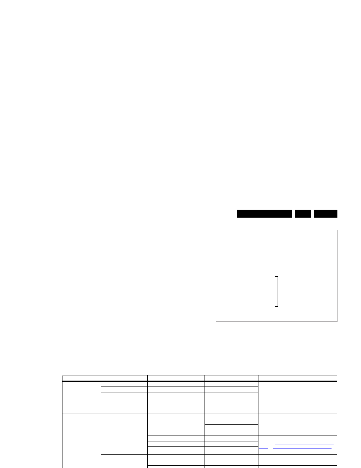
Alignments
EN 43QFU1.2E LA 6.
6.5.1 SSB identification
Whenever ordering a new SSB, it should be noted that the
correct ordering number (12nc) of a SSB is located on a sticker
on the SSB. The format is <12nc SSB><serial number>. The
ordering number of the correct “Service” SSB is the one
preceded by the letter “S” in case 2 or more ordering numbers
are present on the bar code sticker.
Figure 6-1 SSB identification
6.6 Total Overview SAM modes
Table 6-14 SAM mode overview
18310_221_090318.eps
090319
Main Menu Sub-menu 1 Sub-menu 2 Sub-menu 3 Description
Hardware Info A. SW version e.g. “QF2EU_0.49.1.0 Display TV & Standby SW version and CTN serial
number
B. Standby processor version e.g. “STDBY_77.3.11.16”
C. Production code e.g. “see type plate”
Operation hours Displays the accumulated total of operation hours.TV
switched “on/off” & every 0.5 hours is increase one
Errors Displays the most recent errors
Reset error buffer Clears all content in the error buffer
Alignment White point Colour temperature Normal 3 different modes of colour temperature can be
selected
Warn
Cool
White point red LCD White Point Alignment. For values,
see Table 6-5 White tone default settings 46" PFL
series to 6-8 White tone default settings 55" PFL
series
White point green
White point blue
Ambilight Select module
Brightness
Page 44
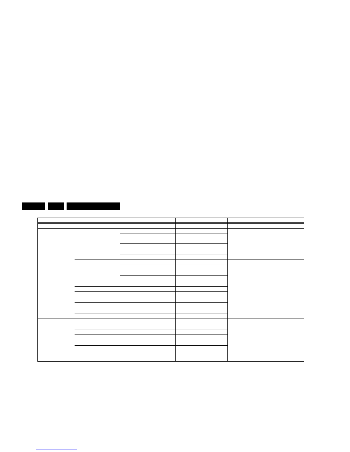
Alignments
EN 44 QFU1.2E LA6.
RF4CE pairing tables Clear paired remote control
Development file
versions
Development 1 file version Display parameters DISPT5.0.9.29 Display information is for development purposes
Acoustics parameters SNDPR
5.0.6.20
PQ parameters FUSIO 1.0.27.22
Ambilight parameters PRFAM 5.0. 5.2
Temp comp parameters 1.3
Development 2 file version 12NC on e zip software Display information is for development purposes
Initial main software
NVM version QF2EU_0.4.5.0
e-Sticker software
Upload to USB Channel list (not) Item “Channel list” removed from the user interface
Personal settings
Option codes
Alignments
Identification data
History list
All (options included)
Download from USB Channel list (not) Item “Channel list” removed from the user interface
Personal settings
Option codes
Alignments
Identification data
All (options included)
NVM editor Type number see type plate NVM editor; re key-in type number and production
code after SSB replacement
Production code see type plate
Main Menu Sub-menu 1 Sub-menu 2 Sub-menu 3 Description
Page 45
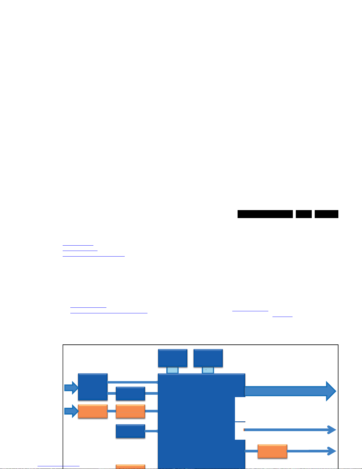
Circuit Descriptions
EN 45QFU1.2E LA 7.
7. Circuit Descriptions
Index of this chapter:
7.1
Introduction
7.2 Power Supply
7.3 General Power Architecture
Notes:
•Only new circuits (circuits that are not published recently)
are described.
• Figures can deviate slightly from the actual situation, due
to different set executions.
• For a good understanding of the following circuit
descriptions, please use the wiring-, block- (see chapter
9.
Block Diagrams) and circuit diagrams (see chapter
10.
Circuit Diagrams and PWB Layouts). Where
necessary, you will find a separate drawing for clarification.
7.1 Introduction
The QFU1.2E LA chassis is part of the FUSION platform and
covers sets in the 6xxx, 7xxx, 8xxx and 9xxx range.
It uses the same chipset as the earlier QFU1.1E LA chassis.
Only circuits that differ from this chassis are described in this
manual. For all other info, refer to the QFU1.1E LA manual.
7.1.1 FUSION 2013 Architecture Overview
For details about the chassis block diagrams refer to
chapter 9.
Block Diagrams. An overview of the FUSION 2013
architecture can be found in Figure 7-1
.
32 16/32
Hybrid
Tuner
DVB-T2
Tuner DVB-S2
CI+
BL uP
Fusion
VByOne OR LVDS
AL
1GB
DDR
1GB
FLASH
GPIO
#mapping
+I2C
Page 46
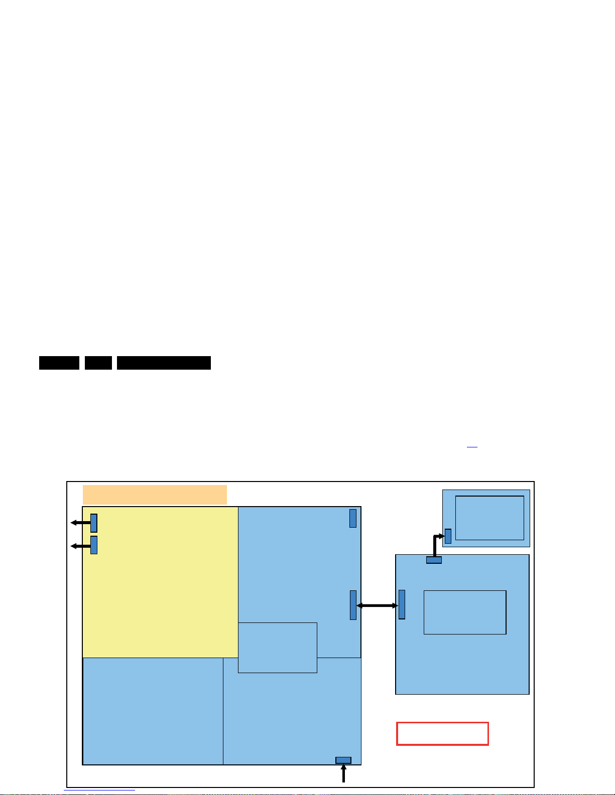
Circuit Descriptions
EN 46 QFU1.2E LA7.
7.2 Power Supply
7.2.1 Power Supply Unit
All power supplies are a black box for Service. When any of
these power supplies is defective, a new board must be
ordered and the defective one must be returned, unless the
main fuse of the board is broken. Always replace a defective
fuse with one with the correct specifications! This part is
available in the regular market.
Consult the Philips Service web portal for the order codes of the
boards.
7.3 General Power Architecture
For the power architecture, refer to figure 7-2
Ac-input +
Mainsfilter
PFC
Display-power
With 16 DRV
Platform
-Power
Display interfacing
1316, 1319
AC-IN
1308
Low Stby
power
Control +
Power
1M90
Ambient
Light
Basic-SSBPlatform
1 power-PCB
1M09
Fully integrated PSLS
19370_084_130208.eps
Page 47
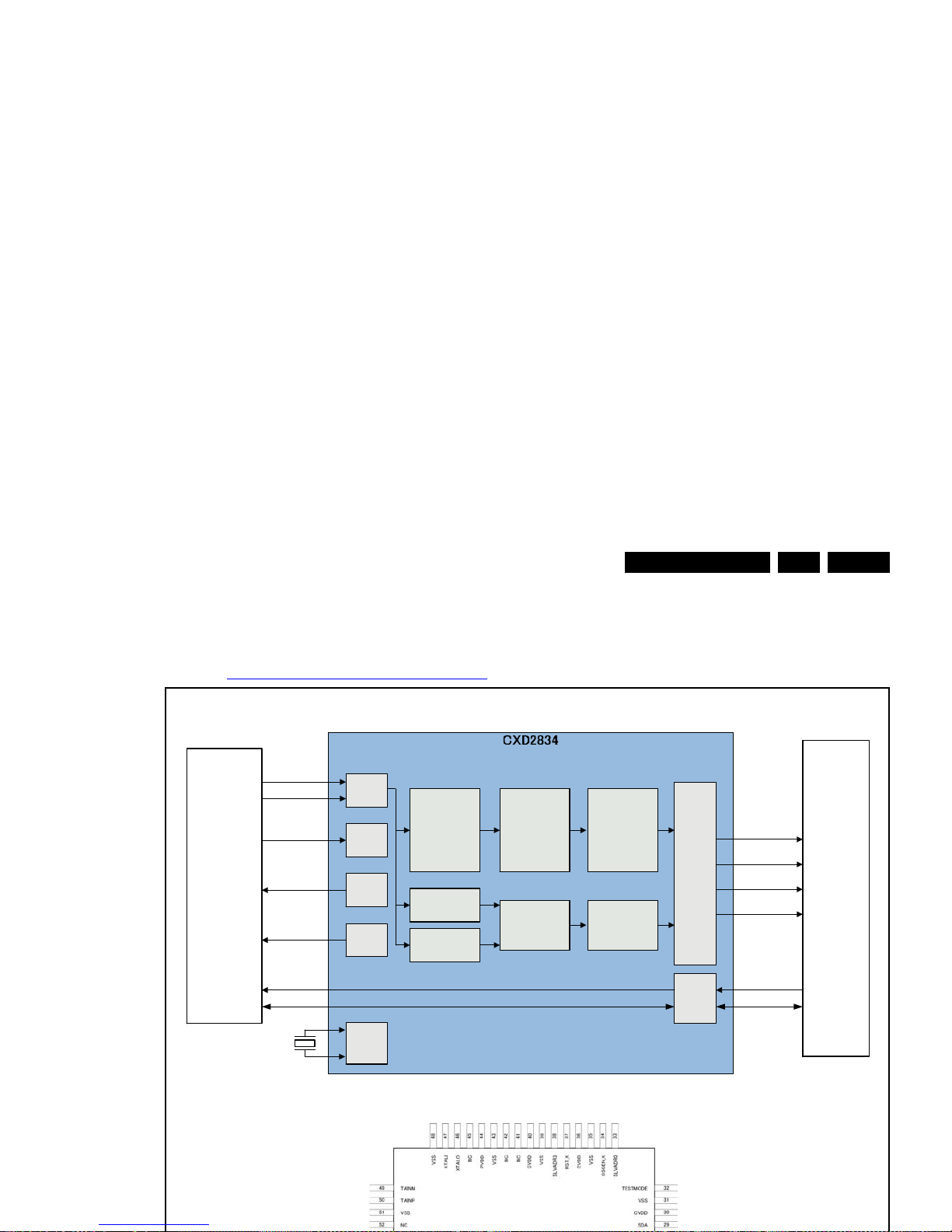
IC Data Sheets
EN 47QFU1.2E LA 8.
8. IC Data Sheets
This chapter shows the internal block diagrams and pin
configurations of ICs that are drawn as “black boxes” in the
electrical diagrams (with the exception of “memory” and “logic”
ICs).
8.1 Diagram 10-1-8 B02C, DVBT2 channel decoder B02C, CXD2834 (IC7KC0)
Block diagram
Pinning information
TSIF
I2C IF
SCL
SDA
RFAIN
TTUSCL
TTUSDA
TAINP (IF)
TAINM (IF)
GPIO1 (PWM)
TIFAGC
XTALI
XTALO
41MHz or
20.5 MHz
IF+
IF-
(RFAGC-MON)
(RFAGC)
IFAGC
SCL
SDA
TUNER
MPEG
Decoder
TSCLK
TSVALID
TSSYNC
TSDATA7-0
TSCLK
TSVALID
TSSYNC
TSDATA7-0
SCL
SDA
DVB-T2
Demodulator
LDPC/BCH
Decoder
Stream
Processor
RS Decoder
TS
Smoothing
DVB-T
Demodulator
DVB-C
Demodulator
OSC
PLL
10-bit
ADC
12-bit
ADC
AGC
GPIO
Page 48
IC Data Sheets
EN 48 QFU1.2E LA8.
Personal Notes:
Page 49

Block Diagrams
EN 49QFU1.2E LA 9.
2014-Jan-10
back to
div. table
9. Block Diagrams
9.1 Wiring Diagram Series 40"
Page 50
EN 50QFU1.2E LA 9.
Block Diagrams
2014-Jan-10
back to
div. table
9.2 Wiring Diagram 42" - 47" 6xxx series
v19374_025_140110.epsvv
Wiring diagram 42"- 47" 6xxx series
Page 51
Block Diagrams
EN 51QFU1.2E LA 9.
2014-Jan-10
back to
div. table
9.3 Wiring Diagram 55" 6xxx series
19374_024_140110.eps
Wiring diagram 55" 6xxx series
Page 52
EN 52QFU1.2E LA 9.
Block Diagrams
2014-Jan-10
back to
div. table
9.4 Wiring Diagram 55" 7xxx series
v19374_026_140110.epsvv
Wiring diagram 55" 7xx8 series
Page 53
Block Diagrams
EN 53QFU1.2E LA 9.
2014-Jan-10
back to
div. table
9.5 Wiring Diagram 60" 6xxx series
19374_023_140110.eps
Wiring diagram 60" 6xxx series
Page 54
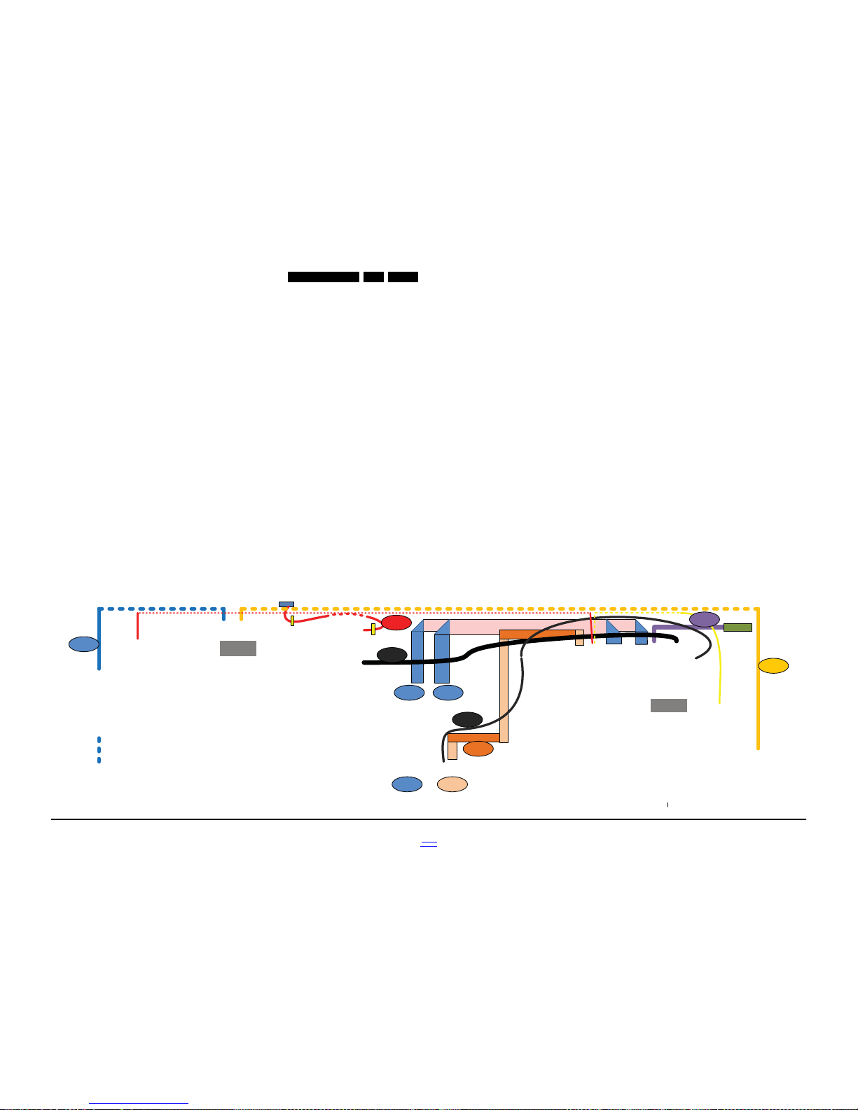
EN 54QFU1.2E LA 9.
Block Diagrams
2014-Jan-10
back to
div. table
9.6 Wiring Diagram 60" 8xxx series
19374_022_140110.eps
Wiring diagram 60" 8xxx series
8C27
PSU
SSB
RF4CE
8C28
8C29
8C31
8G50 8G51
8M09
8M90
8015
8016
8T51
Page 55
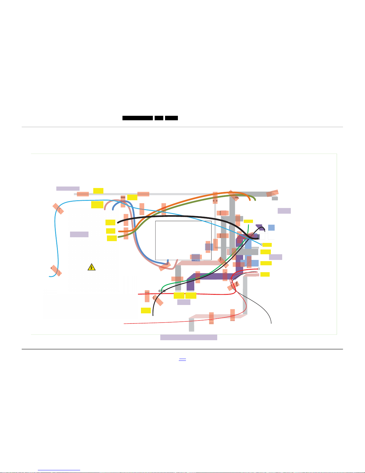
Block Diagrams
EN 55QFU1.2E LA 9.
2014-Jan-10
back to
div. table
9.7 Wiring Diagram 65" 9xxx series
19374_021_140110.eps
Wiring diagram 65" 9xxx series
1050 PSU
809A
809B
8316
8319
8702
8803
8C27
8G50
8G51
8G52 8G53
8M01
8M90
8C20
1012 LED-RECEIVER PANEL
TCON
SSB
FRC
1020 RF4CE
Page 56
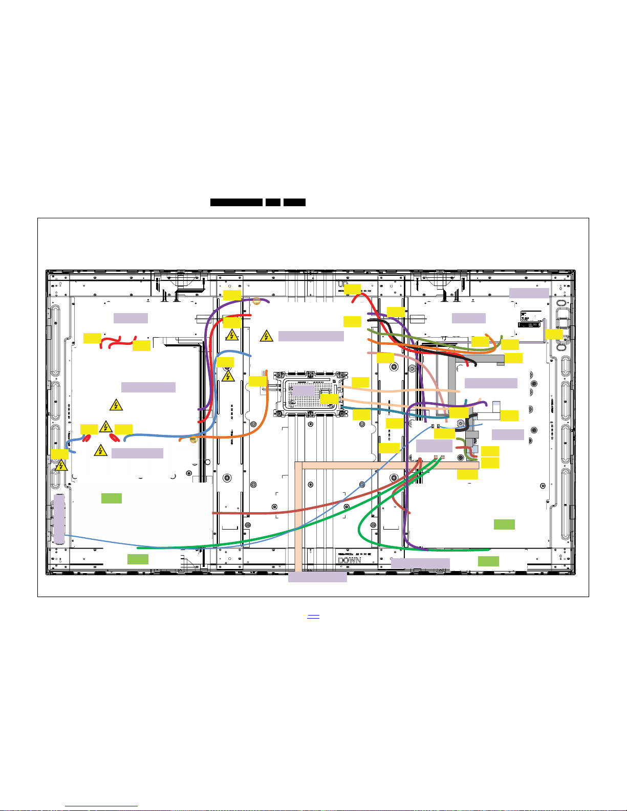
EN 56QFU1.2E LA 9.
Block Diagrams
2014-Jan-10
back to
div. table
9.8 Wiring Diagram 84" 9xx8 Series
19374_015_131126.eps
131126
Wiring diagram 84" 9xx8 series
1050 EMI-boardI
1052 PFC-board
1051 Standby Board
1006 FRC Board
1111 SSB
LED driver
8D01
8D02
8G51
8G50
8S00
8M90
8L24
8M11
5219
5220
TCON
8M01
8C20
8702
8L26
8G52
8G53
8L33
8L32
8P50
8P41
8P40
8P42
8P43
8L11
8L21
1073 Keyboard
1012 LED board
5212
5212
8S01
8M90
8803
1020 RF4CE
8C27
8L25
8L25
Amplifier board
1174
1043 WiFi module
LED driver
Page 57
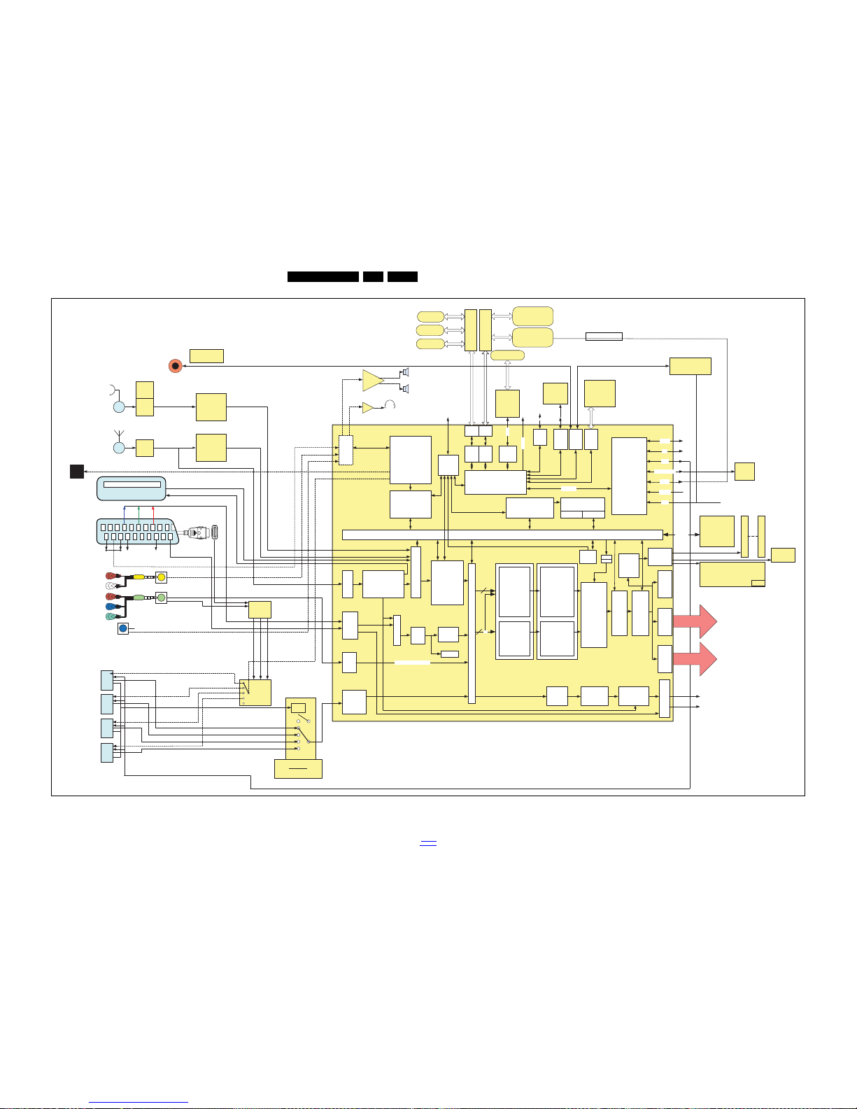
Block Diagrams
EN 57QFU1.2E LA 9.
2014-Jan-10
back to
div. table
9.9 Block Diagram
19370_059_130201.eps
130201
1 3 5791113 15 17
19 21
2468 10 12 14 16 18
20
2/4 LVDS
RGB 1080
× V×1 10
1080
STANDBY POWER ISLAND
74HCT4051
1:8 demux
HDMI
#1
STANDBY
MCU
(8051)
- RTC
- IR decode
- Key pad
- CEC
- Slow ADC
1GB
DDR3
CH DEC
CXD2834ER
SUTRE214
RF In
SmartCard
CA slot (CI+)
CA TS In/ Out
HDMI
#2
L
R
Class D
HP
YPbPr
1GB
8 bit SLC
NAND Flash
Memory
10 bit
p
HDMI-Rx
B1
G1 R1
Status 1
SCART
HDMI
#3
HDMI
#4
CH DEC
SI2169
STV
6111B
Sat In
DVB-T2
DVB-S + S2
TS-DVBS
HDMI mux
SiI9287B (4 inputs)
USB 1
USB-HDD-DM
USB 2
USB-PORTA-DM
Ethernet
S/PDIF-OUT
EDID
HDMI Audio Return Channel (ARC)
HDMI0_ARC
CEC
0
3
2
1
Analog
Audio
AFE
12bit
54MHz
RF4CE module
Ti CC2533
Ethernet
PHY
Atheros
AR8030
10/100Mbit
WoLAN
A
L
1
A
L
n
FBL
UART for
factory/Service
USB 3
USB-PORTB-DM
Optical
S/PDIF
Y
Pb
Pr
L
R
YPbPr
YPbPr
audio
L/R
DVI
audio
L/R
Y3
Y2
Y1
Y0
Y4
HDMI ARC
HDMI ARC
HDMI ARC
Audio
Post-
processing
Audio-Video
Decoder
CPU
MIPS 74kc @700MHz
2 × Channel Memory Bus
EJTAG
AFE
12bit 54MHz
USB
MAC
PLF
MIPS @ 1GHz
USB
MAC
10/100/
1000
Ethernet
MAC
PHY PHY
SDIO
(2)
I2C UART
P-
FLASH
APP CPU
MIPS 74Kf @ 700MHz
Graphics Engine
2D 3D
IMGR
VIF/SIF, ATSC, DVB-
T/C, ISDB-B/QAM
DEMODULATOR
M
U
X
Analog
Video
Mux
AFE:
108MHz
10bit
Analog
Video
Mux
10bit 3D
comb
filter
TRANSPORT DEMUX
MULTI
VIDEO
ENCODER
DECODER
MIPS 4KEc CPU
Video
Decoder
VBI Slicer
S
E
L
E
C
T
Automatic association with:
- HDMI 1/2/3/4 with DVI video
SCART RGB
SCART CVBS
YPbPr
YPbPr L/R Audio
VGA L/R Audio
SCART L/R Audio
Component / PC RGB
TS-DVBT2
Registers
PWM
(3)
/2
64/48bit
Display
CPU
MIPS 24Ke
@ 400MHz
3D BLENDER
- Gamma
- White balance
- 12bit resolution
- RGB
processing
- xvYCC for
main channel
- 2x
programmable
colour matrix
- Bitmask Video
Source Select
Support for 3D
Halo
Free
ME/MC
FRC
Watermark
Insertion
PWM
SPI
IDP
I/F
Quad
LVDS
I/F
Vx1
I/F
Mux
&
6dB
Gain
CVBS Out
Scaler
Video DACTV Encoder
Backlight
Meter
2D Dimming
Ambilight
Fingerprint
detection
IR in
ADC in
GPIO
CEC
I2C
UART
SPI interface
PIP
[...PQ processing...]
MAIN
[...PQ processing...]
PIP
[...PQ processing...]
MAIN
[...PQ processing...]
Main
1080p@60Hz
PIP
1080p@60Hz
8 bit RGB
p
BACKEND
cf. backend requirements
H&V
H&V
OSD Scalers
S1S2 S0
GPIO for WoWLAN
CVBS Not used
LNB
DVB-S2
LNBH25
3D IRL/R + V-sync
Wi-Fi Module
BCM43235 / MIMO 2x2 11n
OR
PCA9554BS
I²C driven
SC1-DETECTn
YPBPR-DETECTn
I2S
Analogue
Stereo
Standby
NVM
512KB flash
NVM
8K×8
EEPROM
Backlight
μP
USB
HUB
USB
HUB
Skype module
camera & mic
USB-CAM-DM
Page 58
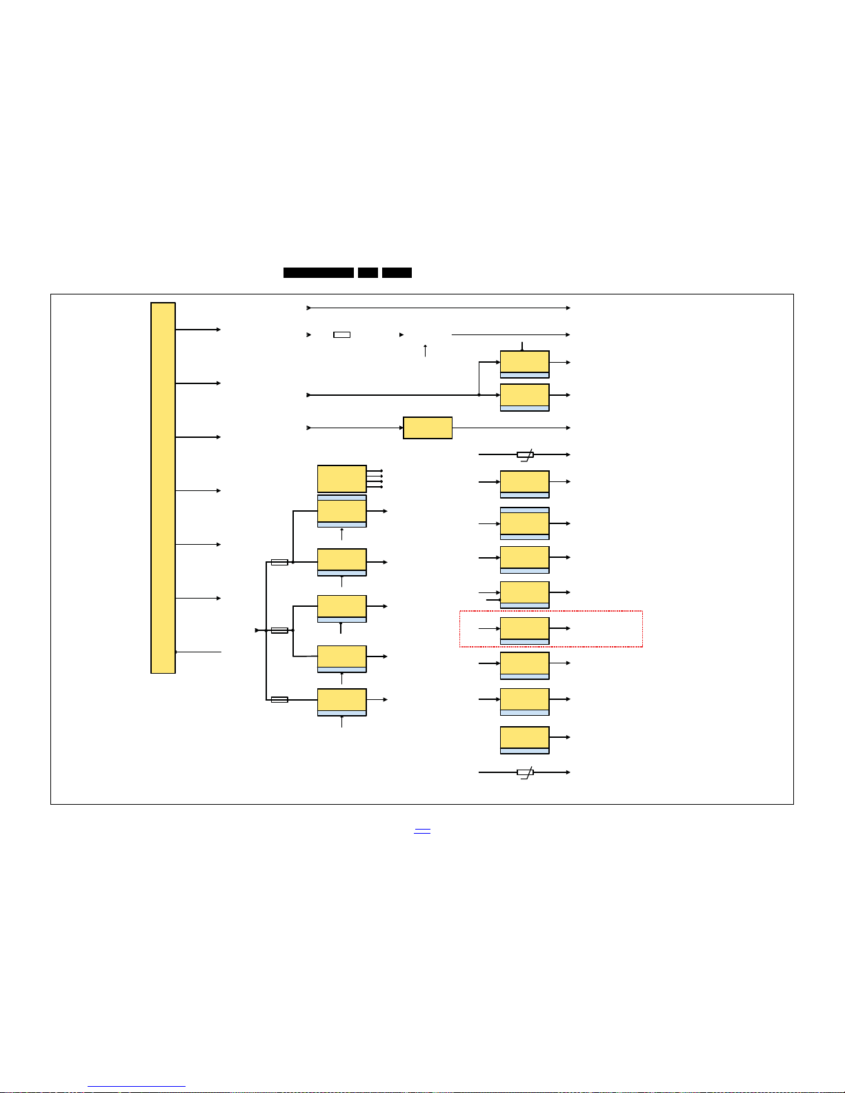
EN 58QFU1.2E LA 9.
Block Diagrams
2014-Jan-10
back to
div. table
9.10 Block Diagram Supplylines
19370_060_130201.eps
130201
12V to 1,1V
switching converter
12V to 1,5V
switching converter
12V to 3,3V
switching converter
12V to 5V
switching converter
+1V1-FD
+1V5
+3V3
+5V
+1V2-FE
+12V
12V to +V-LNB
switching converter
+V-LNB
T 3A 32V
T 3A 32V
T 3A 32V
3,3V to 1,1V
linear regulator
1,5V to 1,2V
linear regulator
3,3V to 1,2V
linear regulator
3,3V to 2,5V
linear regulator
1,5V to 1,1V
linear regulator
+1V1-FA
+1V2-MIPS
+1V2-FA
+2V5
+1V1-DVBT2
1,5V to 1,2V
linear regulator
DVS1
DVS2
5V to 3,3V
linear regulator
VCC-TUNER
5V to 3,3V
linear regulator
+3V3-DVBS
+3V3
+3V3
+3V3
+1V5
+5V
+5V
+1V5
+1V5
+3V3 +3V3AL
over-current protection
1A (2A fuse) or 2,8A
AMBI-POWER+12VAL
(ambilight)
(ambilight)
(Fusion)
(Fusion 2
nd
core voltage)
(Fusion)
(Fusion, PLL)
(DVB-T2, DVB-S2)
(DVB-S2)
(DVB-T/T2)
+12V detector,
power-up and
power-down
sequencer
DETECT12V
ENABLE+1V5+1V1
ENABLE+2V5
ENABLE+3V3
+T
3,5V to 3,37V
linear regulator
3,5V to 3,3V
linear regulator
+3V3-LAN
+3V3-STANDBY
+3V5-STANDBY
((W)LAN)
(Fusion, RC,...)
+12V
T 4A 32V
TCON switch
+VDISP (TCON)
+12V-AUDIO
+12V-AUDIO
(Class-D)
LCD-PWR-ONn
ENABLE-WOLAN
ENABLE+1V5+1V1
ENABLE+1V5+1V1
ENABLE+3V3
DETECT12V
(I2C)
ENABLE+2V5
1M90
+3V5-STANDBY
+12V
+12V-AUDIO
+12VAL
GND-AL
GND
STANDBY
pin 10
pin 9
25 and 26
pins 13 and 14
pins 21 and 22
pins 23 and 24
16, 27 and 28
pins 7, 8, 15,
pins 11, 12,
RT8228DGQW (7UC0)+ ext mosfet
TI TPS54527DDA
RT7297CHZSP
RT8288AZSP
LNBH25LPQ (ST00)
RT9187BGB (RICHTE)
TI TPS7A7001DDA (TI00)
NX1117C12Z (NXP0)
RT9025-12GSP (RICHTE)
RT9025-12GSP (RICHTE)
RT9025-12GSP (RICHTE)
NX1117C33Z (NXP0)
NX1117C33Z (NXP0)
RT9193+33GB (RICHTE)
RT9187GSP (RICHTE)
(chanel decoder)
Reserved
+12Va
+12Vb
(USB )
+5V-PORTA,B, C
+T
1.5A
(0.5A per USB)
1UA0
1UP1
1UA1
Page 59
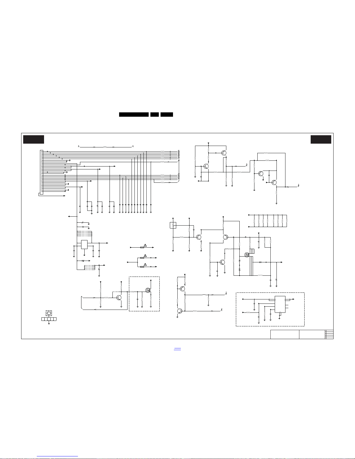
Circuit Diagrams and PWB Layouts
EN 59QFU1.2E LA 10.
2014-Jan-10
back to
div. table
10. Circuit Diagrams and PWB Layouts
10.1 310431366124 SSB
10-1-1 B01A, Power connector
19370_127_130227.eps
130227
Power connector
B01A B01A
2012-11-22
4
3104 313 6612
Power connector
VIN VOUT
GND
FLG
PG
EN
RSET
CSS
COM
OUTIN
EN BP
AMBILIGHT 3-SIDED PROTECTION
RES
+12V DETECTION
optional
5
1
2
9
10
3
4
8
6
11
7
16V
7UAD
SIP32429DN-GE4
2UAT
100u
FUAK
IUAJ
FUAT
FUA2
3UG4-4
100K
2GY7
1n0
2UAA
1u0
FUAU
1M0
3UD0
IUFS
IUFT
3GY8
100R
1u0
2UAR
FUA1
GND-AL
IUF0
2UAW
100n
GND-AL
1u0
2UAM
3UA7
10K
+12VAL
+3V3
3GY5 100R
4K7
FUA4
3UA5
1%
3
2
IUA2
7UAB
BC847BW
1
240R
1%
3UAR
+22V
+12VAL
3UAP-3
4K7
3 6
IUF3
RES
FUA9
10K
3UG9
IUAV
GND-AL
GND-AL
FUAD
1K8
3UGA
1UA1
3UAB
220K
RES
3.0A32VT
100n
2UAS
2
6
1
IUFU
AMBI-POWER
BC857BS(COL)
7UAA-1
IUAP
GND-AL
4K7
3UAN-3
3 6
1%
RES
+12V
100K
3UD1
FUAE
7
8
9
2930
IUAD
23
24
25
26
27
28
3
4
5
6
13
14
15
16
17
18
19
2
20
21
22
1
10
11
12
SMAW200-H28S2
1M90
S1D
9UA1-2
2UF8
1u0
6UAB
RES
3
A
1
K
2
R
GND-AL
RES
7UAF
TS2431
3UA8
100K
100K
+3V3-STANDBY
3UG4-3
2UA4
100p
1UA2
FOR DUAL SIDE AL ONLY
FUAH
22K
3UAF-3
3 6
T63V2.0A
+12VAL
FUA5
3UAL
10K
4K7
3UAP-4RES
45
RES
RES
27
4
123
4K7
3UAP-2
7UAC
5
678
SI4778DY-GE3
1n0
2GY9
IUAA
GND-AL
IUFQ
FUAM
RES
2UAJ
1u0
7
IUF7
3GY1-2
100R
2
3GY6 100R
FUAV
RES
IUAM
9UA2-1 RES
9UA0
GND-AL
+3V3-STANDBY
9UA2-3
RES
FUAF
12K
2
6
1
3UAV-2
1%
10n
BC847BPN(COL)
7UF7-1
8 1
2GY1
FUAA
3UAF-1
22K
6UAC
PDZ15B(COL)
3UG8
22K
+12V
FUAL
+12Va
RES2UA3
100n
+3V5-STANDBY
1X15
REF EMC HOLE
100n
2UAB RES
IUF8
3UA4
100R
FUA6
100R
3GYA
22K
3UG0-2
CUA1
RES
27
2UAD
100n
RES3UAN-2
4K7
FUAN
4K7
3UAN-1
RES
1 8
3UAC
1R0
RES
3UAT-2
10K
100p
2UAN
GND-AL
IUFP
45
+12V
FUAB
3 6
3GY1-4
100R
100R
3GY1-3
GND-AL
2UA2
1u0
IUA3
1n0
2GY6
1n0
2GY5
4
9UA1-3
7UA0-2
BC847BPN(COL)
5
3
3UG0-1
22K
+12VAL
+12VAL
FUAC
9UA1-1
3UAT-1
10K
27
+12V-AUDIO
3UAF-2
22K
IUAF
3u0
5UAA
+12Vb
IUAR
2GY4
1n0
3K3
1%
3UA6
RES
1 8
FUAP
3UAP-1
4K7
1%
3UAV-4
FUAG
+3V3-WIFI
12K
BC857BS(COL)
7UF9-1
3UAV-3
12K
1%
100p
2UAK
3UAK
10K
1u0
2UF6
5
IUAS
3UAN-4
4K7
RES
4
3UG2
22K
10K
3UG0-3
22K
3UAT-4
3UA9
10K
IUAL
2UAL
100p
IUA1
+12VAL
IUAN
1 8
2GYA
1n0
100R
3GY1-1
2GY8
1n0
5
3
4
+12VAL
15
7UF7-2
BC847BPN(COL)
RT9193-33GB
7UF8
43
2
RES
4K7
4
3UAG
3UAF-4
22K
5
7UA2 RES
2
6
1
PMV31XN
+12V
7UA0-1
BC847BPN(COL)
9UA2-2 RES
IUAB
100R
3GYB
1u0
2UA0
3UAS
10K
CUA0
3UAH
47K
68K
3UAE
FUA8
1%
3UAW
0R1
+3V3-STANDBY
AMBI-POWER
+12V-AUDIO
2UF9
100n
6UAF
+3V3
REF
B230LA-M3
1u0
2UAP
1n0
2GY2
100R
3GY7
9UA2-4 RES
IUF1
AMBI-POWER
PDZ15B(COL)
6UAD
3UG4-2
100K
+3V3-STANDBY
RES
3UG3
1K0
IUAK
100R
3GY9
AMBI-POWER
6.3V330u
2UAV
+3V3-STANDBY
RES
2UAU
100n
1UA0
3.0A32VT
2UA1
22u 16V
RES
3
4
7UAA-2
BC857BS(COL)
5
IUF6
+3V3-WIFI
2UA5
10n
RES
IUAT
7UF9-2
BC857BS(COL)
2UF7
22n
IUFR
IUA0
FUA7
FUA3
10n
2GY3
7UA3
BC847BW
10K
3UAT-3
3UAY
100R
1%
IUAC
+12V
3UAV-1
12K
2UA9
330u6.3V
RES
3UG4-1
100K
FUA0
3UG0-4
9UA1-4
POWER-OK
STANDBY
STANDBYn
22K
BL-SPI-CS_BL-I-CTRL BL-I-CTRL
BL-DIM8
BL-DIM5
BL-DIM7
BL-DIM4
BL-DIM6
BL-DIM3
BL-DIM2
BL-I-CTRL
BL-DIM1
STANDBY
ENABLE+1V5+1V1
DETECT12V
ENABLE+3V3
BL-ON
DETECT12V
Page 60
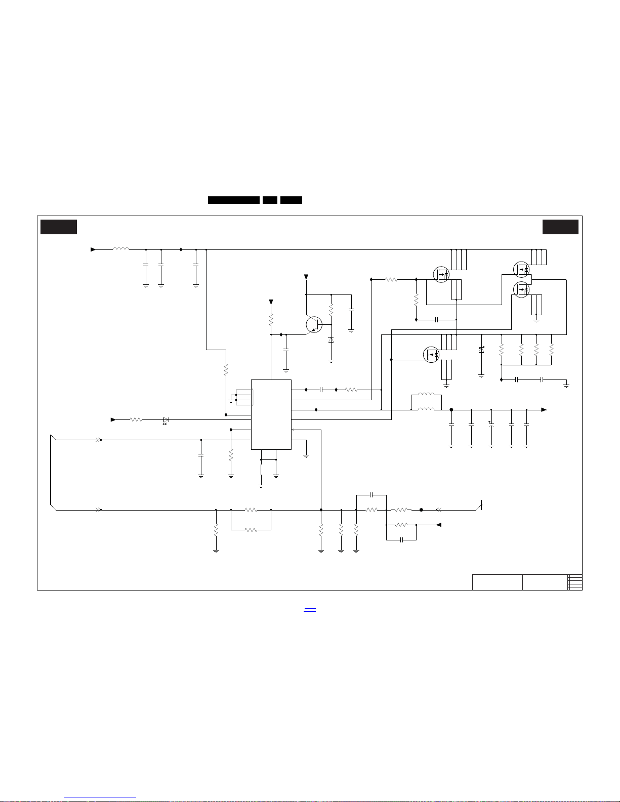
EN 60QFU1.2E LA 10.
Circuit Diagrams and PWB Layouts
2014-Jan-10
back to
div. table
10-1-2 B01B, Fusion supply
19370_128_130227.eps
130227
Fusion supply
B01B B01B
2012-11-22
4
3104 313 6612
Fusion supply
NC
GND_HSGND
BOOT
UGATE
FB
PHASE
LGATE
MODE
TON
PGOOD
CS
EN
VCC
CORE VOLTAGE SUPPLY FUSION
GND-1V1F
3UC4RES
GND-1V1F
1R0
2u0
5UC0
IUC7
3UC2
2K2
+1V1-FD
2UCP
10u
RES
BC847BW
7UC1
+12Va
2UCM
22p
5
IUCB
10R
3UC3-4
4
2UCN
1u0
IUC3
IUC4
22u
2UCB
IUC6
GND-1V1F
1%150K
3UCA
3UCB
22K 1%
220K
3UCN
10R
3UCC
1%
220p
4
123
2UCD
7UC2
SI4778DY-GE3
RES
567
8
4
10
1
8
9
567
7UC4
AON7932
2
3
IUC8
1 8
IUCA
10R
3UC3-1
6UC1
PDZ5.6B(COL)
IUC0
1%12K
3UCP
FUC0
2UCE
10u
2UCL
220u 2.5V
1M0
3UCR RES
1%
2UCF
1n0
3UCF
22K
B340A-M3
IUC1
IUC5
6UC2
3
14
4
7
GND-1V1F
GND-1V1F
15
17
2
10
1
6
9
16
12
RT8228DGQW
5
13
11
8
30R
7UC0
+1V1-FD
5UC1
2UC1
1n0
IUCP
GND-1V1F
2u0
5UC2
10R
3UC3-3
3 6
22u
+12Va
2UCA
22u
2UCK
RES
3UC8
3R3
IUC2
IUC9
2UCH
100n
3R3
1%
3UC1
4
123
3UCE
120K
7UC3
RES
567
8
RES
+5V
GND-1V1F
SI4172DY-GE3
2UCJ
22u
1%180K
3UCG
10R
27
10R
3UCD
RES
3UC3-2
3UC9
2K2
DBG DBG
+5V
22u
2UCC
LTST-C190CKT
6UC0
FUC1
22u
2UCW
2UCY
22u
3UC0
10R
3UC7
270K 5%
1n0
2UCR
DVS1
ENABLE+1V5+1V1
RES
SENSE+1V1-FD
Page 61
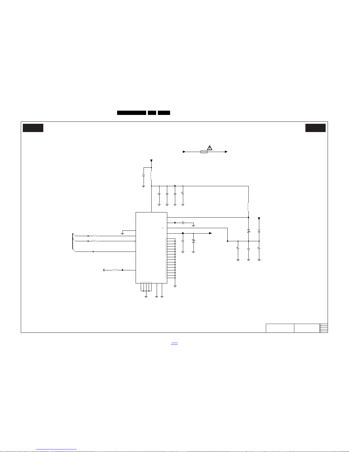
Circuit Diagrams and PWB Layouts
EN 61QFU1.2E LA 10.
2014-Jan-10
back to
div. table
10-1-3 B01C, LNB supply
19370_129_130227.eps
130227
LNB supply
B01C B01C
2012-11-22
4
3104 313 6612
LNB supply
VUP
VOUT
ADDR
VIA
LX
VCC
NC
DSQ
ISEL
GND
PGND
GND_HS
VBYP
SCL
SDA
DSQIN
100n
2UPL RES
+12V-DVBS
T 32V3.0A
1UP1
IUP2
IUPJ
B230LA-M3
2UPE
10u
20
21
6UP6
8
16
17
26
27
28
29
30
31
32
33
1
5
10
11
12
13
14
24
4
7
22
2
1518192325
9
3
Φ
LNBH25LPQ
7UP2
6
47u 25V
+12V-DVBS
+V-LNB
2UPG
10u
2UPD
IUP4
25V47u
2UPF
2UPJ
470n
25V10u
2UPM
+V-LNB
+12V
RES
47R
3UPD
RS1D
6UP5
FUPA
1u0
B230LA-M3
6UP4
2UPH
IUPF
5UP5
10u
30R
5UP6
IUPE
220n
2UPK
3UPE
22K
2UPC
100n
3UPB
47R
SCL-FE
SDA-FE
F22-DISECQ-TX
Page 62
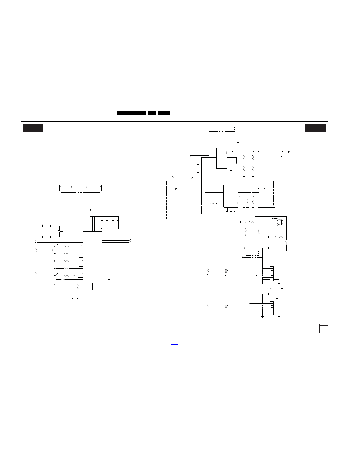
EN 62QFU1.2E LA 10.
Circuit Diagrams and PWB Layouts
2014-Jan-10
back to
div. table
10-1-4 B01D, USB internal
19370_130_130227.eps
130227
USB internal
B01D B01D
2012-11-22
4
3104 313 6612
USB internal
NC
GND
GND
HS
VIN
EN
VIA
VOUT
BP|ADJ
VCC_A_3
VCC_D
XIN
XOUT
DD1DD1+
OVR1
DD2-
VIA3
VIA4
VCC
VCC_A_1
VCC_A_2
DD2+
OVR2
DD3DD3+
OVR3
DD4DD4+
OVR4
VREG
RESET
SELFPWR
GANG
RREF
GND_HS
TEST|SCL
SDA
D-
D+
VIA1
VIA2
GND_HS
VOUT
FB
VIA
VAUX
L
UVLO
EN
PS
VIN
GND
PGND
reserved
RES
2EHS
22u
RES
3EHP
1%120K
100n
2EM2
+5V
+3V3-LAN
3EM3
10K
FEH8
RES9EHE-3
9EH8-1
FEH4
RES
RES9EHE-1
6
78
IEH4
1
2
3
4
5
9EM2
1C31
A1253WRA
+3V5-STANDBY
2EM4
100n
IEH2
680R
RES
5EH0
4u7
IEH0
3EM4
2EHW
10n
47K
3EHV
RES
100n
2EHP
7
10
1
2
3
4
RES
RT9187GSP
7EH2
58
6
9
10u
2EHL
9EM3
RES
3EHT
22K
3EHJ
FEH1
+3V3
+3V3
100K
3EM6
10K
FEH3
IEHJ
IEH3
IEH6
+3V3-WIFI
IEM1
IEM2
+3V3
RES
2EHV
100n
+3V3
3EM1
1M0
FEH2
2EM3
14
21
30
31
32
33
28
10
11
100n
20
19
17
8
26
22
18
2759
12
13
15
16
1
2
23
29
25
24
3
4
6
7
22u
2EHT
7EM1
CY7C65632-28LTXCT
RES
3EM5
100K
IEH5
IEH1
FEH7
2EHY
100u 6.3V
RES
100n
2EHJ
RES9EHE-2
RES
330K
3EHS
3EHU
22K
9EH8-4
RES
9EHE-4
9EM1
RES
1%
+3V3
RES
3EHR
22K
2EHN
100n
RES
+3V3
2EM5
12M
1EM0
100n
22u
2EHR
RES
cEH0
RES
FEH6
3EHN
10K
10K
3EM8
10K
3EM7
18p
2EM1
100n
2EM7
2EM6
100n
3
4
5
67
RES
2EHU
1n0
1C30
A1253WRA
1
2
18p
FEH9
2EM0
+3V3
1%10K
3EM0
7EHJ
BC847BW
+3V5-STANDBY
1M0
3EHY
2
2EH9
47n
9
11
3
4
8
7
1
12
13
5
7EH4
TPS61200DRCG4
016
2EHM
10u
RES
FEH5
RES
+3V3-LAN
+3V3
9EH8-2
RES
9EH8-3
1%33K
3EHW
3EM9
10K
USB-WIFI-DP
ENABLE-WOLAN
+3V3-LAN
MD-IFIW-BSUMD-1BSU
PD-IFIW-BSUPD-1BSU
USB-WIFI-DM
IRQ-WOLANn
USB-CAM-DM
USB-CAM-DP
USB1-DM
USB1-DP
RESET-FUSION-OUTn
USB-CAM-DM
USB-CAM-DP
USB-WIFI-DM
USB-WIFI-DP
Page 63
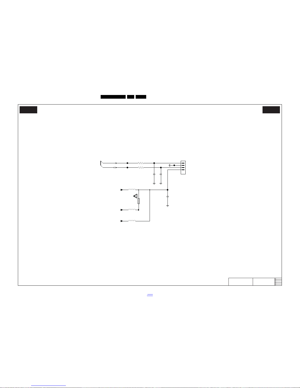
Circuit Diagrams and PWB Layouts
EN 63QFU1.2E LA 10.
2014-Jan-10
back to
div. table
10-1-5 B01E, Miscellaneous
19370_131_130227.eps
130227
Miscellaneous
B01E B01E
2012-11-22
4
3104 313 6612
Miscellaneous
SENSOR
TEMPERATURE
FTA3
5TA3
30R
2
3
4
RES
A1253WRA
1T71
1
FTA1
+3V3-STANDBY
1TA1
1.0A
RES
+12V
63VT
10R
3TA2
RES
FTA6
FTA5
ITA1
RES
5TA1
30R
30R
5TA2
RES
FTA2
FTA4
10R
3TA1
RES
1u0
2TA3
RES
2TA2
10p
2TA1
RES
10p
+3V3
RES
SCL-SRF
SDA-SRF
Page 64
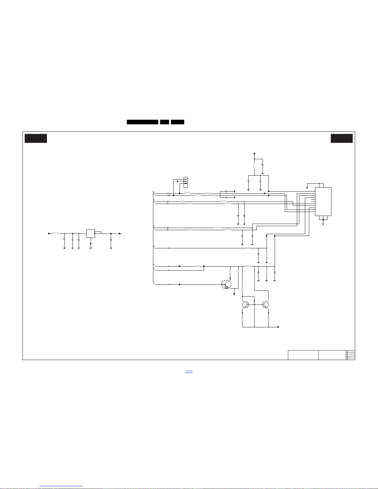
EN 64QFU1.2E LA 10.
Circuit Diagrams and PWB Layouts
2014-Jan-10
back to
div. table
10-1-6 B02A, Hybrid T/C tuner
19370_132_130227.eps
130227
Hybrid T/C tuner
B02A B02A
2012-11-22
4
3104 313 6612
Hybrid T/C tuner
COM
OUTIN
10p
2FAC
RES
6.3V330u
2FA0
2
6
1
7FA1-1
BC857BS(COL)
10p
2FAG
2FA8
100n
RES3KA2
6K8
2FAE
10p
2FAD
22n
FFA3
2FAA
10p
2FA5
22u 16V
5FA1
30R
2FA7
10p
VCC-TUNER
FFA5
FFA4
IFA3
10K
3FAB
4
5FAA
30R
7FA1-2
BC857BS(COL)
5
3
FFA2
1
3
2
4
7FAA
LD1117S33
VCC-TUNER
100R
3KA3
3FAC
470R
PDTA114EU
7KA0
RES
IFA6
FFAC
330n
5FA4
RES3FA8
6K8
2FAF
10p
3FA4
47R
3KA4
100R
RES
FFAD
3FA1
100R
3KA0
47R
FFA6
5FA6
30R
IFA5
10p
2FA9
FFA8
IFAA
FFAA
FFA9
FFAB
VCC-TUNER
IFA4
2FAH
10p
47R
3KA1
14
15
16
NC1
5
NC2
6
10
I2C_SCL
11
I2C_SDA
IF1_N
3
IF1_P
2
8
IF2_N
IF2_P
7
12
13
1F00
SUT-RE214Z
TUNER
A3.3V
1
AGC1
4
AGC2
9
FFA7
2FA3
1n0
470R
3FAA
1FA0
BM03B-SRSS-TBT
1
2
3
45
3FA2
DBG
100R
2FA2
100n
VCC-TUNER
3FAD
2K7
2FAB
10p
+5V
FFAE
5FA5
330n
2FA1
10u
5FA7
30R
22K
3KA5
2K7
3FA9
5KA1
3FA3
330n
47R
100R
RES
330n
5KA0
3FA7
SCL-FE
SDA-FE
SOC-IF-AGC
AGC-SWITCH
IF-AGC-DVBT2
IF-AGC-DVBT2
SOC-IF-N
SOC-IF-P
IF-N-DVBT2
IF-P-DVBT2
Page 65
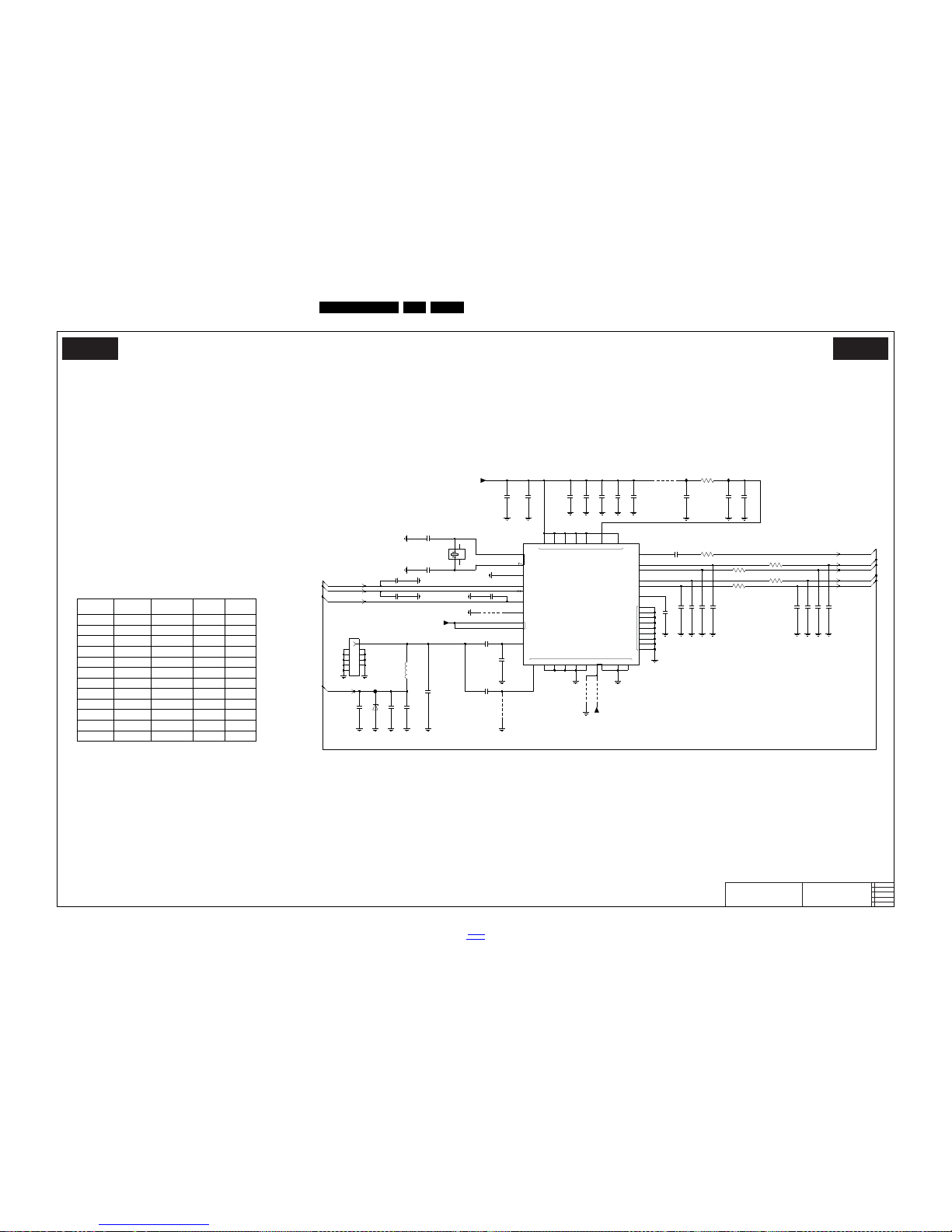
Circuit Diagrams and PWB Layouts
EN 65QFU1.2E LA 10.
2014-Jan-10
back to
div. table
10-1-7 B02B, Satellite tuner
19370_133_130227.eps
130227
Satellite tuner
B02B B02B
2012-11-22
4
3104 313 6612
Satellite tuner
NC
VCO
XTAL_OUT
VIA
IP
NC
RF_OUT
QN
QP
IN
RF LNA LT MIX DIG BB SYN HS
GND
VCOLNA LT MIX DIG BB SYN
VSS
XTAL_IN
XTAL_CMD
SCL
SDA
AGC
AS
RF_IN
-
68P
-
-
27
Diversity Matrix (Satellite Tuner dependant)
X
3RB3
27
2RBW
Affected Pin
27
X
I2C-ADDRESS : C6
100P
Default Value
X
X
2RBV
27P
25
2RBU
-
X
JUMP
X
2RBY
JUMP
2RB1
-
27
-
STV6111
X
27
9RB8
4,5
-
9RB9
10U
-
2K2
X33N
4,52RBM
STV6110
-
7
4N7
X
2RB7
4,5
4R7
JUMP
27P
4,5
9RB6
9RB7
Position Nr
-
X
25
X
JUMP
X
-
10p
2RBA
+3V3-DVBS
2RBP
10p
2RBN
10p
*
2RB6
100n
27
27p
2RBM
*
100R3RB1-2
2RBU
4n7
10n
2RBK
2RB2
1n0
1K0
3RB0
*
10
2RB1
27p
1
2
3
4
5
6
7
8
9
*
1R01
9RB7
IRB0
100p
2RBY
*
2RBL
22u
100R
1 8
+3V3-DVBS
3RB1-1
10p
2RBC
2RBB
10p
4R7
3RB3
*
2RB7
*
10u
2RBS
10p
10p
2RBR
*
3 6
2RBW
33n
3RB1-4
45
3RB1-3 100R
100R
2RBV
68p
*
IRB1
10p
2RBF
2RBE
10p
+3V3-DVBS
3n3
2RBD
*
2RB9
10p
9RB6
24
1
3
16M
NX3225JB
1RB0
5RB0
27n
2RBJ
1n0
RES
SM15T
6RB0
10p
2RK0
2RBH
100p
2RK1
10p
RES
2RB5
100n
31
32
34
35
36
37
38
39
40
41
42
1
30
7
12
13
2214 82118627
25 26
19
18
23
24
20
21
5
4
7RB0
2
16
17 3351920193
STV6110AT
TUNER
SATELLITE
Φ
RES 2RBG
0p56
9RB8
*
1n0
2RB3
2RB4
1n0
100p
2RB8
RES
47p
2RBT
*
RES
9RB0
FRB0
9RB9
+V-LNB
XTAL
DVBS-IP
DVBS-IN
DVBS-QP
DVBS-QN
DVBS-AGC
SCL-S-TUNER
SDA-S-TUNER
Page 66
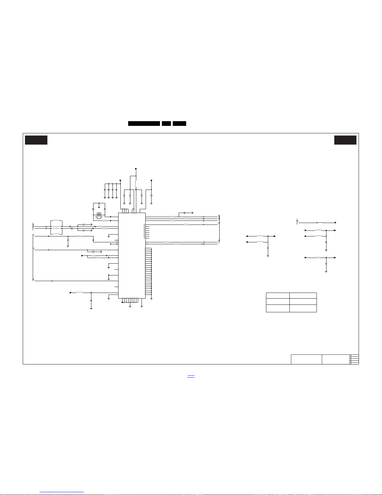
EN 66QFU1.2E LA 10.
Circuit Diagrams and PWB Layouts
2014-Jan-10
back to
div. table
10-1-8 B02C, DVBT2 channel decoder
19370_134_130227.eps
130227
DVBT2 channel decoder
B02C B02C
2012-11-22
4
3104 313 6612
DVBT2 channel decoder
NC
PVDD
DVDDCVDD
VSS
GND_HS
TSDATA
SDA
VIA
TSCLK
TSVALID
TSSYNC
0
1
2
3
4
5
6
7
SCL
XTALO
TAINP
TAINM
RFAIN
GPIO0
GPIO1
GPIO2
TIFAGC
TTUSCL
TTUSDA
TESTMODE
SLVADR0
OSCEN_X
RST_X
SLVADR3
NC1
NC2
XTALI
+1V1-DVBT2
+1V2
CXD2834
0XD8
+1V1
ADDRESS
7KC0
GAIA3
=
I2C
IKC6
IKC7
2KC5
100n
IKC4
2KC0
100n
+1V2-DVBT2-C
VCC-TUNER
1K0
3KC4
RES
9KC0
30R
5KC5
+1V2-DVBT2-C
DKC1
IKC2
+3V3-DVBT2-D
IKC1
5KC6
30R
47p
2KCG
2KCD
47p
IKC0
47R
3KC1
10K
3KC7
DKC0
+1V2-DVBT2-C
2KCP
1u0
2KCR
1u0
10n
RES
2
4
13
2KCH
100n
2KC4
1KC0
41M
3KC9
3K3
3K3
3KC8
+3V3
+1V2-DVBT2-C
2KCC
12p
72
47R
3KC0-2
8
1
IKC3
IKC8
3KC0-1
47R
47R
3KC3
2KCF
100n
+1V1-DVBT2+3V3-DVBT2-D
100n
2KC1
IKC9
43
35
34
57
58
6
11182327313639
69
70
71
72
73
74
52
53
54
55
56
59
60
61
62
63
64
65
66
67
68
51
13
14
15
16
17
3
4
46
45
50
30
37
38
24
48
5
8
9
12
47
2
33
40
26
32
41
29
20
21
25
1022284471942
49
1
+3V3-DVBT2-D
7KC0
CXD2834ER
100n
2KC7
2KC6
100n
1K0
3KC6
6 3
22R
3KCE
47R
3KC0-3
30R
5KCA
2KCK
6p8
RES
100n
2KC3
FKC1
2KC2
100n
IKCB
30R
5KC9
4u7
5KC1
12p
2KCB
30R
RES
5KC7
5KC8
30R
RES
2KCL
100n
RES
3KCB
47R
47R
3KCA
+3V3-DVBT2-D
+1V2-DVBT2-P
100n
2KCE
IKC5
2KCJ
100n
9KC1
5KC0
4u7
+1V2-FE
+1V2-DVBT2-P
IKCA
10u
2KCS
3KC2
47R
SENSE+1V1-DVBT2
TS-CHDEC-CLK
TS-CHDEC-DATA
SCL-FE
SDA-FE
IF-P-DVBT2
IF-N-DVBT2
AGC-SWITCH
IF-AGC-DVBT2
TS-CHDEC-VALID
TS-CHDEC-SOP
RESET-FUSION-OUTn
Page 67
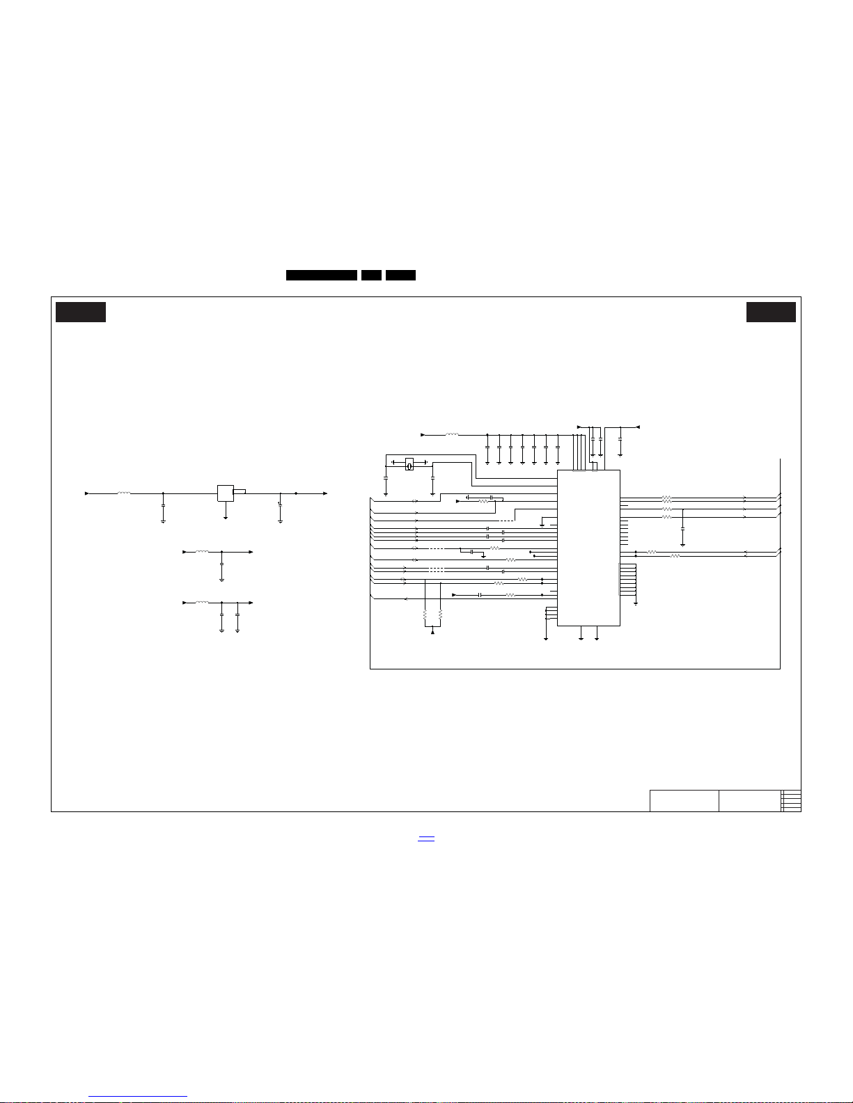
Circuit Diagrams and PWB Layouts
EN 67QFU1.2E LA 10.
2014-Jan-10
back to
div. table
10-1-9 B02D, DVBS/S2 channel decoder
19370_135_130227.eps
130227
DVBS/S2 channel decoder
B02D B02D
2012-11-22
4
3104 313 6612
DVBS/S2 channel decoder
COM
OUTIN
NC
GND_HS
TS_ERR|GPIO_1
TS_CLK
TS_DATA0|TS_SER
TS_DATA1
TS_DATA2
TS_DATA3
TS_DATA4
TS_DATA5
TS_DATA6
TS_DATA7
SDA_HOST
SCL_HOST
VIA
S_ADC_QP
S_ADC_QN
MP_A
MP_B
MP_C
MP_D
TC_ADC_P
TC_ADC_N
SDA_MAST
SCL_MAST
DISEQC_CMD
DISEQC_IN
DISEQC_OUT
GND1|JTAG_TCLK
GND2|JTAG_TDI
GND3|JTAG_TDO
GND4|JTAG_TRSTB
GND5
VDD_VANA
VDD_VIO
VDD_VCORE
TS_SYNC
TS_VAL
XTA_I|CLK_IN
XTA_O
CLK_IN_OUT
RESETB
GPIO_0|JTAG_TMS
ADDR
RSSI_ADC
S_ADC_IP
S_ADC_IN
1
324
LD1117S33
7RDA
2RD8
IRDA
100n
IRD0
1 83RD6
10K
3RD0-1
47R
3RD1
47R
100n
2RDH
+3V3-DEMOD
FRDA
47R
3RD8
DRD1
5RDA
30R
10n
2RDN
2RD1
100n
2RDA
100n
4
1 3
1RD0
NX3225JB
16M
2
2RDC
6p8
4K7
3RDB
RES
RES
3RD4
47R
22u
2RDS
IRD1
DRD0
3RD2
10K
RES
3RDA
4K7
1K0
3RD9
5RDB
+1V2-FE
30R
+3V3-DEMOD
+V-LNB
53
54
55
56
57
58
33
32
+3V3-DVBS
36
72028489
22
50
51
52
17
18
19
23
24
25
26
13
12
45
38
37
40
39
42
41
14
15
16
49
3
1
2
29
30
31
43
10
46
11
34
44
4
5
6
8
21
27
47
35
SI2169-A10-GM
7RD0
9RD3
+5V
100p
2RDT
5RDD
30R
2RD4
100n
100n
2RD3
2RD0
100n
3RD7
47R
9RD0
IRD6
+3V3-ANA
2RD6
100n
5RDC
30R
2RD2
100n
27
+3V3-DVBS
47R
3RD0-2
22u
2RDM
IRD5
100n
2RDP
2RDDRES
10p
+3V3-ANA
9RD2
16V22u
2RDR
100n
2RD7
IRDC
22u
2RDJ
2RDL
22u
RES
2RDF
100n
+3V3-DVBS
100n
2RD9
22u
2RDK
IRD2
RES
47R
3 6
IRDB
3RD0-3
100n
+3V3-DEMOD
2RDB
47R
3RD5
+3V3-DEMOD
2RDG
100n
2RD5
10K
3RD3
100n
IRD3
9RD1
AGC-SWITCH
SDA-S-TUNER
SCL-S-TUNER
RES 2RDE
10p
DVBS-AGC
F22-DISECQ-TX
DVBS-IN
IF-P-DVBT2
IF-N-DVBT2
IF-AGC-DVBT2
XTAL
TS-DVBS-DATA
TS-DVBS-CLK
TS-DVBS-SOP
TS-DVBS-VALID
RESET-FUSION-OUTn
DVBS-QP
DVBS-QN
DVBS-IP
SCL-FE
SDA-FE
Page 68
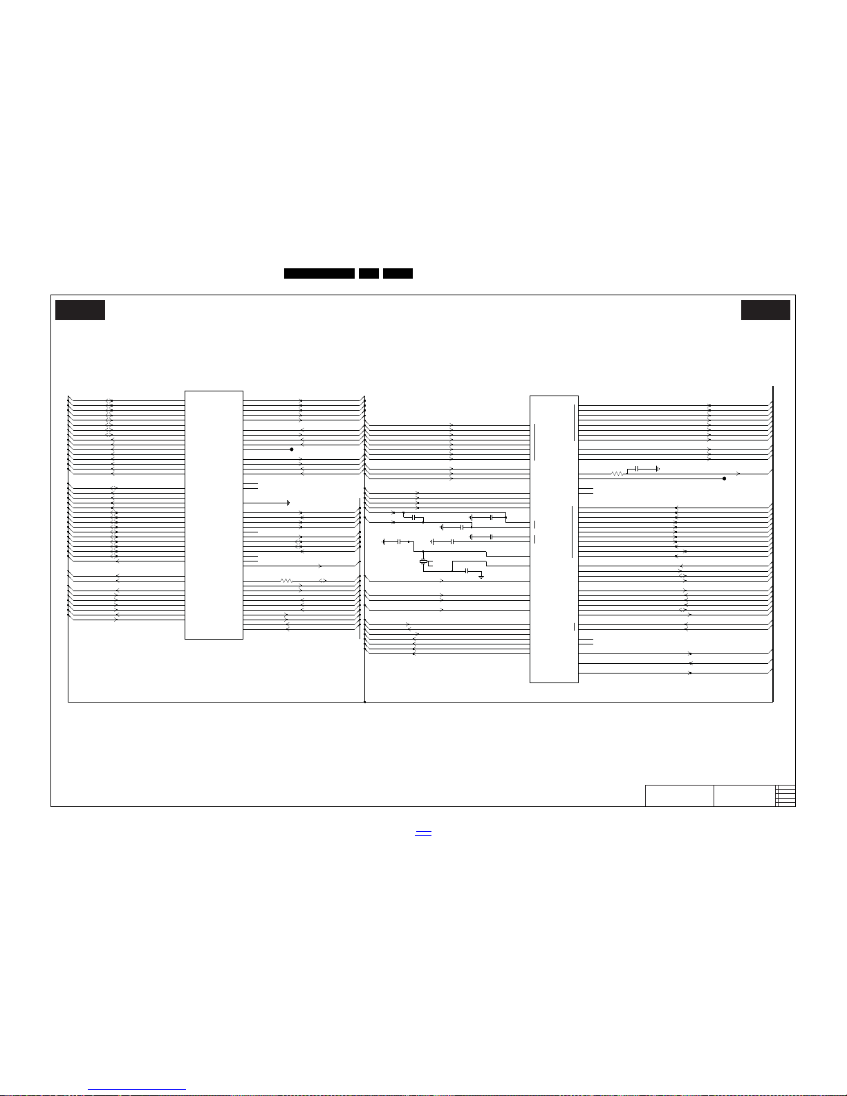
EN 68QFU1.2E LA 10.
Circuit Diagrams and PWB Layouts
2014-Jan-10
back to
div. table
10-1-10 B03A, Fusion
19370_136_130227.eps
130227
Fusion
B03A B03A
2012-11-22
4
3104 313 6612
Fusion
FRA13_CLE
FRA14_ALE
FRA15_PODA14
FOE
FWE
BOOTCS
FCE2N
FINT1
FINT2
FCLK
FAVD_PODA6
FREADY
FRD0_PODD0
FRD1_PODD1
FRD2_PODD2
FRD3_PODD3
FRD4_PODD4
FRD5_PODD5
PODA4
PODA5
POD_A7
POD_A8
FRD10_PODA2
FRD11_PODA3
FRD12_PODA10
FRD13_PODA11
FRD14_PODA12
FRD15_PODA13
FRA0_AD0
FRA1_PODWE
FRA2_PODIORD
FRA3_PODIOWR
FRA4_PODREG
FRA5_AD1
FRA6_AD2
FRA7_AD3
FRA8_AD4
FRA9_PODOE
FRA10_AD5
FRA11_AD6
POD_A9
PODIREQ
PODRST
PODVS1
PODWAIT
POD_DIR
PODCE1
PODCE2
PODCD1
POD_CD2
POD_VCC_EN
POD_VPP_EN
HPD
FRA12_AD7
FRD6_PODD6
FRD7_PODD7
FRD8_PODA0
FRD9_PODA1
LGSEN
CEC
PWRON
PCVS
XTLI24M
XTLO24M
TSSDEN
TSSSYNC
TSSCLK
TSSDI
TS1CLK
TS1SYNC
TS1DEN
TESTMOD
STB_EN
SPI_EN
SFSI
SFSO
N
PD
P
N
IN
0
1
2
3
SFWPN
SFHOLDN
SFCES
SFSCK
STB_SDA
STB_SCL
LED
IR
KYBRD
5
6
7
TS1D
TS2OD
1
2
AVLINK
MUTE
HP_DETECT
STB_RSTO
PCHS
STB_RXD
STB_TXD
0
1
2
3
4
5
6
7
8
DGPIO2
DGPIO1
TAGCO_RF
TAGCO_IF
TS2ODEN
TS2OSYNC
TS2OCLK
RSTN
TESTCON
9
10
STB_GP
P
4
5
6
7
0
1
2
3
4
AF30
AE28
AF22
AJ23
AH23
AD30
AE30
AE29
AD29
A11
GPIO8
A10
GPIO9
R30
AJ22
AH22
AF29
AD28
AD27
AE27
AG30
A12
GPIO22
B13
GPIO23
D10
GPIO24
C9
GPIO3
B9
GPIO4
B8
GPIO5
A7
GPIO6
B11
GPIO7
C12
GPIO15
D12
GPIO16
C13
GPIO17
E10
GPIO18
D11
GPIO19
C10
GPIO2
E11
GPIO20
B12
GPIO21
AF25
AG26
AG23
AK24
B7
GPIO0
B10
GPIO1
C11
GPIO10
A9
GPIO11
A13
GPIO14
AE25
AH26
AH28
AF24
AF26
AE24
AK25
AH25
AH27
AK27
AJ25
AH29
AJ29
AF28
AH30
AG28
AJ30
AJ28
AJ27
AK23
AK26
AG25
AK28
AK29
AG29
AF27
AG27
AG24
AE23
AK22
AJ26
AD26
FLASH_CI_GPIO
FUSION240
7J00-6
AJ24
AG22
AE26
AH24
AF23
FJ10
4n7
2FZ5
4
1 3
1J00
24M
2
U30
H30
H29
AK18
AE19
AF19
AG19
AH19
AJ19
AF20
AE20
U29
T26
U28
AJ20
AK20
AE21
AF21
AG21
AH21
AE22
AK21
AK19
AH18
AJ18
P28
P27
R27
F27
G26
P30
P29
AJ21
AG20
AH20
P26
M25
N30
N29
N28
N27
N26
N25
P25
J29
R28
J26
L29
L27
L30
L28
L26
K30
K28
H25
M27
M26
M29
J30
J25
M30
H26
J28
J27
E27
E28
R29
7J00-7
FUSION240
TS_TSB_MCU
K25
K26
M28
T28
T29
K27
F29
F30
2FZ2
10p
18p
2J11
2FZ6
47p
RES
100n
2FZ3
10p
2FZ1
18p
2J10
FJ16
3FZ0
100R
3FZ1
33R
CA-CE2n
CA-CE1n
GPIO14
2FZ4
100n
MDI3
MDI4
MDI5
MDI6
MDI7
MIVAL
MISTRT
TS-CHDEC-CLK
TS-CHDEC-VALID
TS-CHDEC-DATA
TS-CHDEC-SOP
F-CEn
SOC-IF-AGC
RESET-STANDBYn
GPIO17
CA-MOCLK
CA-MDO0
CA-MDO1
CA-MDO2
CA-MDO3
CA-MDO4
CA-MDO5
CA-MDO6
CA-MDO7
CA-MOVAL
CA-MOSTRT
MICLK
MDI0
MDI1
MDI2
LGSEN
AUDIO-MUTEn
PWRON
SF-CS
SF-HOLDn
SF-CLK
SF-SDI
SF-SDO
SF-WP
SPI-EN
ENABLE-STANDBY
STB-GP0
STB-GP1
STB-GP10
STB-GP2
STB-GP3
STB-GP4
STB-GP5
STB-GP6
STB-GP7
STB-GP8
STB-GP9
STB-RSTO
STB-RXD
STB-SCL
STB-SDA
STB-TXD
TEST-CON
TEST-MOD
CA-A05
CA-CD1n
CA-RDY
CA-RST
CA-VS1n
CA-WAITn
CA-A07
CA-A08
CA-A09
CA-CD2n
AVLINK1
AMBI-TEMP-FUS
HDMI-CEC
HP-DETECT
IF-IN-N
IF-IN-P
IR
KYBRD
LED
F-WEn
GPIO0
GPIO1
GPIO11
GPIO15
GPIO16
GPIO18
GPIO19
GPIO2
GPIO20
GPIO21
GPIO22
GPIO23
GPIO24
GPIO3
GPIO5
GPIO6
GPIO7
GPIO8
CA-A04
CA-OEn
CA-D00
CA-A02
CA-A03
CA-A10
CA-A11
CA-A12
CA-A13
CA-D01
CA-D02
CA-D03
CA-D04
CA-D05
CA-D06
CA-D07
CA-A00
CA-A01
F-RDY
CA-A06
TS-DVBS-DATA
TS-DVBS-CLK
TS-DVBS-VALID
TS-DVBS-SOP
F-OEn
FRA0
FRA10
FRA11
FRA12
NAND-CLE
NAND-ALE
CA-A14
CA-WEn
CA-IORDn
CA-IOWRn
CA-REGn
FRA5
FRA6
FRA7
FRA8
Page 69
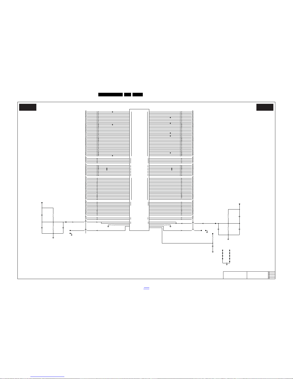
Circuit Diagrams and PWB Layouts
EN 69QFU1.2E LA 10.
2014-Jan-10
back to
div. table
10-1-11 B03B, Fusion Umac controller
19370_137_130227.eps
130227
Fusion Umac controller
B03B B03B
2012-11-22
4
3104 313 6612
Fusion Umac controller
N
P
N
P
N
P
3
MM1ODT
MM1RESETN
MM1CSN
8
7
6
5
4
3
2
P
N
0
1
MZQ1
MM1ANA_TEST
DDR_RETN
15
14
13
12
11
10
9
8
7
6
5
4
3
2
1
0
N
P
MM1DM
MM1DQS0
MM1DQS1
MM1DQS2
MM1DQS3
MM1A
MM1BA
2
1
0
31
MM1RASN
MM1WEN
MM1CKE
26
25
24
23
22
21
20
19
18
17
16
15
14
13
12
11
10
9
13
14
15
0
1
2
MM0CASN
1
0
MM0ANA_TEST
MZQ0
2
1
0
N
0
1
MM0DQ
MM0DM
MM0A
MM0BA
MM0CK
MM0VREF
MM0DQS0
MM0DQS1
P
N
MM0DQS2
P
N
MM0DQS3
MM1DQ
21
22
23
24
25
26
27
MM1CK
MM1VREF
MM1CASN
30
29
28
27
3
P
N
P
N
0
1
2
3
4
5
6
7
8
9
10
11
12
31
0
1
2
0
1
2
MM0RASN
MM0WEN
MM0CKE
MM0ODT
MM0RESETN
MM0CSN
P
3
4
5
6
7
8
9
10
11
12
13
14
15
16
17
18
19
20
28
29
30
1K0
FJ02
3J03
FJ05
FJ04
2J02
100n
FJ03FJ01
3J06
1K0
AE7 T7
3J00
240R1%
N3
AA2
AA3
V3
V4
N1
M3
H4
U7
U6
N2
V5
Y4
R3
U1
P1
U3
L5
R4
T3
T2
N4
AC2
Y2
AC1
U5
AA4
T5
Y5
U4
W5
V1
P5
M5
R5
M4
P4
W1
AB1
Y3
AB3
R1
Y1
K3
J2
J1
J4
T1
P3
AA1
W3
P2
V2
L4
H5
F5
H2
G3
F4
E1
M1
J5
K1
L3
L2
F2
K5
G1
L1
G5
F1
K2
H1
H3
F3
AJ10
AF1
AF2
AG4
AH4
AG11
AF12
AG15
AE11
AE12
AF11
AJ1
AK8
AH6
AJ8
AK5
AK11
AF9
AK6
AK7
AK10
AD3
AD1
AD2
AK4
AG3
AJ3
AK2
AK3
AJ2
AJ5
AG5
AG9
AF10
AG8
AH10
AH9
AG1
AF3
AE3
AH1
AH7
AH2
AJ14
AK14
AG14
AJ6
AK9
AE1
AH3
AH8
AH5
AJ11
AF15
AF17
AJ15
AH16
AG17
AD18
AG12
AF14
AK13
AH12
AH13
AJ12
AJ17
AF13
AK16
AK12
AF16
AK17
AJ13
AK15
AH15
AH17
7J00-8
FUSION240
DDR3
AA7
100n
2J07
100n
DB86
2J06
DB85
1%240R
3J01
2J00
100p
DB80
DB75
1K0
3J05
100n
2J042J03
+1V5-M1
100n
DB82
DB83
DB73
DB47
DB71
DB14
DB74
DB88
DB87
DB81
DB78
DB79
DB46
DB16
1K0
3J04
DB89
+1V5-M1
DB72
100n
2J05
DB76
DB77
+1V5-M0
3J02
1K0
M0-MA0
M0-MVREF0
M1-MVREF1
M0-MA2
M0-MA15
M0-MA14
M0-MA13
M0-MA12
M0-MA11
M0-MA10
M0-MA1
MM0ANA
M0-MA9
M0-MA8
M0-MA7
M0-MA6
M0-MA5
M0-MA4
M0-MA3
M0-CS#
M0-MCLK0
M0-MCLK0#
M0-CKE
M0-CAS#
M0-BA2
M0-BA1
M0-BA0
M0-MD15
M0-MD14
M0-MD1
M0-MD0
M0-DQM3
M0-DQM2
M0-DQM1
M0-DQM0
M0-DQS#2
M0-DQS1
M0-DQS#1
M0-DQS0
M0-DQS#0
M0-MD31
M0-MD2
M0-MD11
MM1ANA
M0-WE#
M0-RESET#
M0-RAS#
M0-ODT
M0-DQS3
M0-DQS#3
M0-DQS2
M0-MD8
M0-MD7
M0-MD6
M0-MD5
M0-MD4
M0-MD3
M0-MD13
M0-MD12
M0-MD20
M0-MD19
M0-MD18
M0-MD17
M0-MD16
M0-MD10
M0-MD9
M0-MD28
M0-MD27
M0-MD26
M0-MD25
M0-MD24
M0-MD2
3
M0-MD22
M0-MD21
M1-MA13
M1-MA12
M1-MA11
M1-MA10
M1-MA1
M1-MA0
M0-MD30
M0-MD29
M1-MA7
M1-MA6
M1-MA5
M1-MA4
M1-MA3
M1-MA2
M1-MA15
M1-MA14
M1-MCLK0#
M1-CKE
M1-CAS#
M1-BA2
M1-BA1
M1-BA0
M1-MA9
M1-MA8
M1-MD0
M1-DQM3
M1-DQM2
M1-DQM1
M1-DQM0
M1-CS#
M1-MCLK0
M1-DQS#1
M1-DQS0
M1-DQS#0
M1-MD31
M1-MD2
M1-MD15
M1-MD14
M1-MD1
M1-RAS#
M1-ODT
M1-DQS3
M1-DQS#3
M1-DQS2
M1-DQS#2
M1-DQS1
M1-MD5
M1-MD4
M1-MD3
M1-MD13
M1-MD12
M1-MD11
M1-WE#
M1-RESET#
M1-MD18
M1-MD17
M1-MD16
M1-MD10
M1-MD9
M1-MD8
M1-MD7
M1-MD6
M1-MD26
M1-MD25
M1-MD24
M1-MD23
M1-MD22
M1-MD21
M1-MD20
M1-MD19
MM0ANA
MM1ANA
M1-MVREF1
DDR-RTN
M0-MVREF0
M1-MD30
M1-MD29
M1-MD28
M1-MD27
Page 70
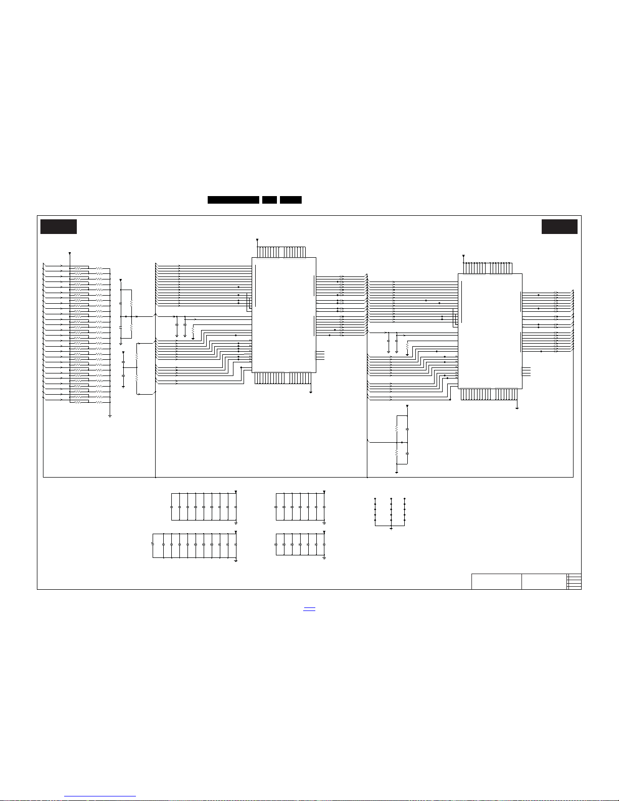
EN 70QFU1.2E LA 10.
Circuit Diagrams and PWB Layouts
2014-Jan-10
back to
div. table
10-1-12 B03C, Umac 1 DDR3
19370_138_130227.eps
130227
Umac 1 DDR3
B03C B03C
2012-11-22
4
3104 313 6612
Umac 1 DDR3
7
15
8
9
10
11
12
13
14
VREFDQ
VREFCA
ZQ
BA0
BA1
BA2
RAS
DQSL
ODT
2
1
0
DMU
DML
RESET
WE
CS
6
5
NC
4
3
CK
CK
CKE
7
BC
AP
VSS
VSSQ
VDD VDDQ
0
1
2
3
4
5
6
DQSU
DQU
0
1
2
3
4
5
6
7
DQL
A
CAS
DQSU
DQSL
7
15
8
9
10
11
12
13
14
VREFDQ
VREFCA
ZQ
BA0
BA1
BA2
RAS
DQSL
ODT
2
1
0
DMU
DML
RESET
WE
CS
6
5
NC
4
3
CK
CK
CKE
7
BC
AP
VSS
VSSQ
VDD VDDQ
0
1
2
3
4
5
6
DQSU
DQU
0
1
2
3
4
5
6
7
DQL
A
CAS
DQSU
DQSL
10n
2J86
3J1D
100R
100R
3J25
3J2B
100R
DB64
DB91
FJ08
3J2L
100R
10u
2J25
100R
3J1R
3J1Z
100R
100R
3J1U
DB53
2J1B
100n
100R
3J1A
DBA7
10n
2J88
100n
2J21
100R
3J2C
G1
G9
L3
L8
J8
M1
M9
P1B1B9
D1
D8
E2
E8
F9
M8
H1
A9
P9
T1
T9
B3
E1
G8
J2
R9A1A8C1C9D2E9F1H2
H9
J3
T2
B2D9G7K2K8N1N9
R1
C3
C8
C2
A7
A2
B8
A3
J1
J9
L1
L9
K1
F8
H3
H8
G2
H7
F3
G3
C7
B7
D7
M3
K3
J7
K9
K7
L2
E7
D3
E3
F7
F2
P3
N2
P8
P2
R8
R2
T8
R3
M2
N8
H5TQ2G63BFR-PBC
7J01
N3
P7
L7
R7
N7
T3
T7
M7
100R
3J2J
+1V5-M1
DB41
+1V5-M1
10n
2J1H
+1V5-M1
3J23
100R
100R
3J2N
10n
2J89
100R
3J2A
3J1T
100R
100R
3J22
75R
3J17
2J85
10n
100R
3J2H
3J18
100R
2J1U
100n
100R
3J29
DB63
3J2G
100R
2J84
10n
3J28
100R
10n
2J1J
10n
2J83
3J20
100R
3J2T
100R
100R
3J1W
DB44
10n
2J81
+1V5-M1
3J24
100R
100R
3J21
100R
3J2M
100n
2J18
+1V5-M1
3J14
1K0
DB51
2J82
10n
+1V5-M1
47u
2J27
16V
2J19
100n
100n
2J1L
2J1K
10n
3J13
240R
100R
3J19
DB59
3J1S
100R
DB38
3J1C
100R
100n
2J1W
100n
2J1A
100R
2J1P
3J27
100n
10n
2J1E
DB62
DB36
2J14
100n
DB55
+1V5-M1
2J87
10n
DBA4
DB01
D1
D8
E2
E8
F9
G1
G9
L3
L8
B3
E1
G8
J2
J8
M1
M9
P1B1B9
D2E9F1H2H9
M8
H1
A9
P9
T1
T9
K2
K8N1N9R1R9A1A8C1C9
A3
J1
J9
L1
L9
K1
J3
T2
B2
D9
G7
G3
C7
B7
D7
C3
C8
C2
A7
A2
B8
E7
D3
E3
F7
F2
F8
H3
H8
G2
H7
F3
R2
T8
R3
M2
N8
M3
K3
J7
K9
K7
L2
R7
N7
T3
T7
M7
P3
N2
P8
P2
R8
H5TQ2G63BFR-PBC
7J02
N3
P7
L7100R
3J1N
DB92
10n
2J1D
3J1B
100R
DB56
DB58
3J1K
100R
DB52
100n
2J1Q
DB49
100n
2J1V
3J2Q
100R
FJ09
240R
3J10
100n
2J15
100n
DB54
2J20
DB45
2J12
10n
RES
1K0
3J11
100R
3J1J
DB40
DB99
DB34
DB32
DB96
3J1M
3J2P
100R
100R
3J16
75R
100R
3J1V
3J2F
100R
100R
3J1E
100R
3J26
3J1Y
100R
DB57
3J1L
100R
DB48
DBA3
2J1N
100n
2J1F
10n
+1V5-M1
DB35
DB94
+1V5-M1
100R
3J2D
3J1P
100R
1K0
3J15
DBA6
2J1S
100n
DB66
DB90
DB98
2J24
10u
DB95
2J1Z
100n
DBA8
DBA2
DB42
DB43
DB97
3J1G
100R
DBA5
2J1G
10n
2J1C
10n
100n
DB50
2J1M
100n
2J17
100n
2J1T
3J2R
100R
2J16
100n
DB31
DB93
DB33
DBA1
100R
3J2E
100R
3J1H
3J1F
100R
2J1R
100n
10u
2J22
DB65
+1V5-M1
DB39
3J2K
100R
100R
3J2S
3J12
1K0
M1-MD17
M1-MD18
M1-MD19
M1-MD20
M1-DQM1
M1-MD26
M1-MD25
M1-MD24
M1-MD29
M1-MD21
M1-MD22
M1-MD23
M1-MD16
M1-MD0
M1-MD7
M1-MD2
M1-MA15
M1-MA15
M1-MD28
M1-MD31
M1-MD30
M1-MD27
M1-DQS#1
M1-DQS0
M1-DQS#0
M1-MD1
M1-MD4
M1-MD3
M1-MD6
M1-MD5
M1-MD15
M1-MD12
M1-MD11
M1-MD8
M1-MD9
M1-MD10
M1-MD13
M1-DQS1
M1-CS#
M1-ODT
M1-CKE
M1-RESET#
M1-MD14
M1-MA8
M1-MA9
M1-MA10
M1-MA11
M1-MA12
M1-MA13
M1-MA14
M1-MA15
M1-BA0
M1-BA1
M1-BA2
M1-RAS#
M1-CAS#
M1-WE#
M1-MCLK0
M1-MCLK0#
M1-MA0
M1-MA1
M1-MA2
M1-MA3
M1-MA4
M1-MA5
M1-MA6
M1-MA7
M1-RESET#
DDR-MVREF12
M1-WE#
M1-RAS#
M1-DQM2
M1-DQM3
DDR-MVREF12
M1-CAS#
M1-MCLK0
M1-CKE
M1-MCLK0#
M1-CS#
M1-DQS3
M1-DQS#3
M1-DQS2
M1-DQS#2M1-MA14
M1-ODT
M1-MA10
M1-MA11
M1-MA12
M1-MA13
M1-MA2
M1-MA3
M1-MA4
M1-MA5
M1-MA6
M1-MA7
M1-MA8
M1-MA9
M1-BA0
M1-BA1
M1-BA2
M1-ODT
M1-RESET#
DDR-MVREF11
M1-WE#
M1-RAS#
M1-DQM0
DDR-MVREF11
M1-MA0
M1-MA1
M1-MA0
M1-MA1
M1-MA10
M1-MA11
M1-MA12
M1-MA13
M1-MA14
M1-MA2
M1-MA3
M1-MA4
M1-MA5
M1-MA6
M1-MA7
M1-MA8
M1-MA9
M1-BA0
M1-BA1
M1-BA2
M1-CAS#
M1-MCLK0
M1-CKE
M1-MCLK0#
M1-CS#
Page 71
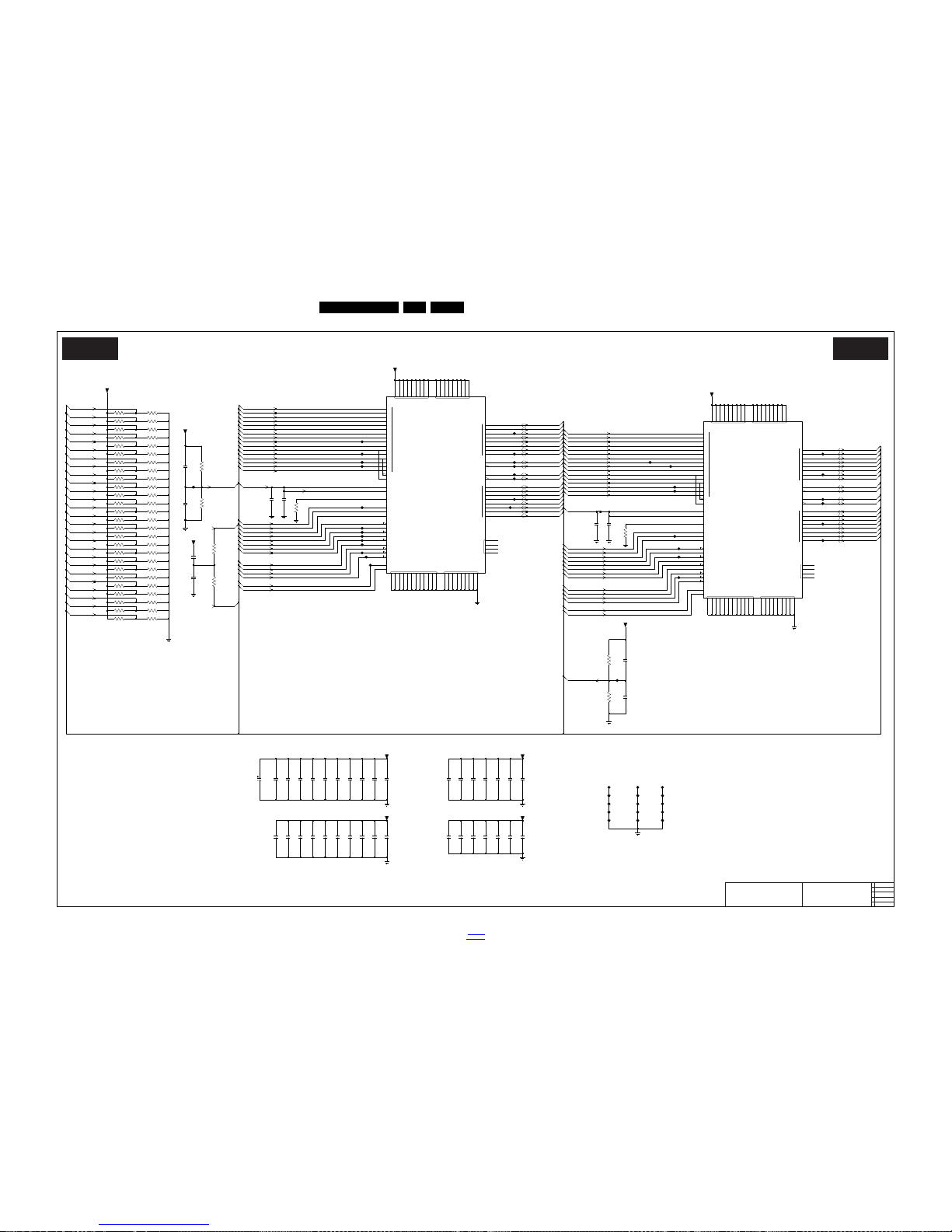
Circuit Diagrams and PWB Layouts
EN 71QFU1.2E LA 10.
2014-Jan-10
back to
div. table
10-1-13 B03D, Umac 0 DDR3
19370_139_130227.eps
130227
Umac 0 DDR3
B03D B03D
2012-11-22
4
3104 313 6612
Umac 0 DDR3
7
15
8
9
10
11
12
13
14
VREFDQ
VREFCA
ZQ
BA0
BA1
BA2
RAS
DQSL
ODT
2
1
0
DMU
DML
RESET
WE
CS
6
5
NC
4
3
CK
CK
CKE
7
BC
AP
VSS
VSSQ
VDD VDDQ
0
1
2
3
4
5
6
DQSU
DQU
0
1
2
3
4
5
6
7
DQL
A
CAS
DQSU
DQSL
7
15
8
9
10
11
12
13
14
VREFDQ
VREFCA
ZQ
BA0
BA1
BA2
RAS
DQSL
ODT
2
1
0
DMU
DML
RESET
WE
CS
6
5
NC
4
3
CK
CK
CKE
7
BC
AP
VSS
VSSQ
VDD VDDQ
0
1
2
3
4
5
6
DQSU
DQU
0
1
2
3
4
5
6
7
DQL
A
CAS
DQSU
DQSL
DB70
1K0
3J2W
DB68
3J3A
100R
3J3V
100R
DBA9
+1V5-M0
100R
3J3U
3J47
DB08
100R
100R
3J4G
100R
3J4F
DBB3
DBB2
DBC1
DBC0
DB03
10n
2J01
DB18
RES
100R
3J3Z
3J36
100R
100R
2J2L
10n
F9
G1
G9
L3
L8
3J3N
J2
J8
M1
M9
P1B1B9
D1
D8
E2
E8
H9
M8
H1
A9
P9
T1
T9
B3
E1
G8
R1R9A1A8C1C9D2E9F1
H2
L9
K1
J3
T2
B2D9G7K2K8N1N9
C3
C8
C2
A7
A2
B8
A3
J1
J9
L1
F2
F8
H3
H8
G2
H7
F3
G3
C7
B7
D7
N8
M3
K3
J7
K9
K7
L2
E7
D3
E3
F7
M7
P3
N2
P8
P2
R8
R2
T8
R3
M2
7J03
N3
P7
L7
R7
N7
T3
T7
10n
2J2V
H5TQ2G63BFR-PBC
DBB5
DBB9
DB22
DB21
3J4E
100R
100R
3J3B
3J3W
100R
2J3B
100n
2J2G
10n
DB15
3J31
1K0
DBC4
100R
3J38
+1V5-M0
DB02
2J3A
100n
DB00
DB13
DB12
100n
2J32
3J45
100R
2J2E
100n
3J2V
1K0
10u
2J3H
100R
3J48
3J3S
100R
FJ0A
DBB6
DB24
3J2Z
100R
1%
240R
3J3M
100R
3J4K
DBB7
3J33
75R
3J41
100R
3J37
2J2Z
10n
DBC7
100R
2J29
100n
2J2C
100n
2J35
100n
+1V5-M0
3J4D
100R
100n
2J37
100n
2J36
DB07
100n
2J2A
2J2W
10n
3J3E
100R
3J40
100R
2J2T
10n
DB29
10n
2J2K
DB61
DB23
+1V5-M0
+1V5-M0
100R
3J43
100n
2J28
2J2M
10n
100R
3J3G
3J3R
100R
+1V5-M0
DB04
DB11
DBC5
DBC6
DB69
100R
DB26
DB25
3J4M
3J4L
100R
DBB1
100R
3J4P
DBB0
100R
100R
3J3T
3J35
100R
3J3P
10n
2J2J
2J3E
100n
2J2B
100n
2J3F
10u
100R
3J44
3J3L
3J46
100R
100R
3J4J
100R
100R
3J3F
2J3J
10u
100n
2J3D
100n
2J3C
DB19
DB20
1%
3J2U
240R
DBC3
DB10
DBC2
DB17
DB30
DBB8
2J2N
DBB4
10n
+1V5-M0
100R
3J4C
1K0
3J30
FJ0B
100n
2J2F
G9
L3
L8
+1V5-M0
M9
P1B1B9
D1
D8
E2
E8
F9
G1
A9
P9
T1
T9
B3
E1
G8
J2
J8
M1
A1A8C1C9D2
E9F1H2
H9
M8
H1
T2
B2D9G7
K2K8N1N9R1
R9
C2
A7
A2
B8
A3
J1
J9
L1
L9
K1
J3
H3
H8
G2
H7
F3
G3
C7
B7
D7
C3
C8
J7
K9
K7
L2
E7
D3
E3
F7
F2
F8
N2
P8
P2
R8
R2
T8
R3
M2
N8
M3
K3
N3
P7
L7
R7
N7
T3
T7
M7
P3
+1V5-M0
7J04
H5TQ2G63BFR-PBC
3J4A
100R
3J3J
100R
DB27
100R
3J4B
2J2Y
10n
3J3D
100R
100n
2J33
DB09
DB67
100R
3J34
100R
3J4H
2J31
100n
3J39
100R
3J3K
2J2H
10n
100R
47u
2J3K
16V
DB05
2J34
100n
100R
3J3C
2J2P
10n
100n
2J2D
3J49
100R
3J3H
100R
+1V5-M0
10u
2J3G
3J32
75R
10n
2J2R
10n
2J2U
3J42
100R
100n
2J39
2J2S
10n
100R
3J3Y
2J38
100n
100R
3J4N
M0-MCLK0#
10n
2J30
M0-RESET#
M0-MA15
M0-MA15
M0-DQM1
M0-MCLK0
M0-MA11
M0-MA12
M0-MA13
M0-MA14
M0-MA15
M0-BA0
M0-BA1
M0-BA2
M0-RAS#
M0-CAS#
M0-WE#
M0-CS#
M0-ODT
M0-CKE
M0-MA0
M0-MA1
M0-MA2
M0-MA3
M0-MA4
M0-MA5
M0-MA6
M0-MA7
M0-MA8
M0-MA9
M0-MA10
M0-MD17
M0-MD21
M0-MD19
M0-MD22
M0-RAS#
M0-DQM2
M0-DQM3
DDR-MVREF02
M0-MA14
M0-ODT
M0-RESET#
DDR-MVREF02
M0-WE#
M0-MD16
M0-MD18
M0-MD20
M0-MD23
M0-MD27
M0-MD30
M0-MD31
M0-MD24
M0-DQS3
M0-DQS#3
M0-DQS2
M0-DQS#2
M0-BA1
M0-BA2
M0-CAS#
M0-MCLK0
M0-CKE
M0-MCLK0#
M0-CS#
M0-MD29
M0-MD28
M0-MD25
M0-MD26
M0-MA0
M0-MA1
M0-MA10
M0-MA11
M0-MA12
M0-MA13
M0-MA2
M0-MA3
M0-MA4
M0-MA5
M0-MA6
M0-MA7
M0-MA8
M0-MA9
M0-BA0
M0-MD7
M0-MD2
M0-MD1
M0-MD6
M0-MD3
M0-RAS#
M0-DQM0
DDR-MVREF01
M0-DQS#1
M0-DQS0
M0-DQS#0
M0-MA14
M0-ODT
M0-RESET#
DDR-MVREF01
M0-WE#
M0-MD0
M0-MD5
M0-MD4
M0-MD12
M0-MD9
M0-MD10
M0-MD11
M0-MD14
M0-MD13
M0-MD8
M0-DQS1
M0-MA0
M0-MA1
M0-MA10
M0-MA11
M0-MA12
M0-MA13
M0-MA2
M0-MA3
M0-MA4
M0-MA5
M0-MA6
M0-MA7
M0-MA8
M0-MA9
M0-BA0
M0-BA1
M0-BA2
M0-CAS#
M0-MCLK0
M0-CKE
M0-MCLK0#
M0-CS#
M0-MD15
Page 72
EN 72QFU1.2E LA 10.
Circuit Diagrams and PWB Layouts
2014-Jan-10
back to
div. table
10-1-14 B03E, Fusion
19370_140_130227.eps
130227
Fusion
B03E B03E
2012-11-22
4
3104 313 6612
Fusion
TXD
RXD
SDAM1
SCLM2
SDAM2
SCLM3
SDAM3
TCK
TMS
TDO
TDI
TRSTN
SCLS
SDAS
SCLM1
TX6_P
TX6_N
TX7_P
TX7_N
HTPDN
LOCKN
IDP_HPD
H_BK_LITE
PWM0
PWM1
BOOST
BKLGON
TCON_ON
TX0_P
TX0_N
TX1_P
TX1_N
TX2_P
TX2_N
TX3_P
TX3_N
GBE_MDC
GBE_MDIO
RX0_P
RX0_N
RX1_P
RX1_N
RX2_P
RX2_N
RXC_P
RXC_N
HEAC
PWR5V
RREF
D1_P
D1_N
USBPPON1
TXRTUNE1
D2_P
D2_N
USBPPON2
TXRTUNE2
GBE_RXD0
GBE_TXD0
GBE_RXD1
GBE_TXD1
GBE_RXD2
GBE_TXD2
GBE_RXD3
GBE_TXD3
GBE_RXC
GBE_TXC
GBE_RXEN
GBE_TXEN
TX4_P
TX4_N
TX5_P
TX5_N
PR_R3
Y_G4
PB_B4
PR_R4
FS1
FB1
FS2
AR_1
AL_1
AR_2
AL_2
AR_3
AOR2
AOL2
SCKI2SOUT
WSI2SOUT
I2SCLK
SPDIFO
FB2
AL_3
AR_4
AL_4
AR_5
AL_5
AR_6
AL_6
SCKIN
WSI2SIN
SDI2SIN
SPDIFIN
GPANA1
CVBS
CVBS2
CVBS3
CVBS4
C
Y_G1
PB_B1
PR_R1
Y_G2
PB_B2
PR_R2
Y_G3
PB_B3
1
2
3
1
2
SDI2SOUT
CVBS_OUT
HPHOL
HPHOR
SUBO
SPK_AOR1
SPK_AOL1
3J55
10R
9GA2
3J09
10R
IJ13
IJ11
3J53
10R
10R
3J52
IJ10
E12
D13
C14
Y28
Y29
AA28
D1
AA26
U26
AA27
E2
AA25
U27
D14
E13
I2C
UART_JTAG
7J00-9
FUSION2403J54
10R
FJ0H
10R
3J50
B20
C20
D20
AA29
AB28
A26
D26 E26
B25
A25
C21
Y27B26
A20
B19
C19
D19
A18
B18
C18
D18
Y26C26
AA30
A14
B14
B17
A17
C17
D17
AC28
B21
A21
Y25
A19
A22
E22
A23
E23
A24
E24
C16
C15
A15
B16
A16
B22
D22
B23
D23
B24
D24
C25
D25
AV_IN_OUT
FUSION240
7J00-4
C5
A5
B5
B6
A6
C6
C7
AB27
AC27
AB26
AB25
B30
C8
B2
A2
C2
C3
A3
B3
B4
A4
C4
D2
T30
C29
B29
A29
B28
A28
B27
A27
C30
V29
V28
V27
V26
V30
T27
D4
A8
D5
E5
E4
AC29
AC30
W25
Y30
V25
W29
W28
W27
W26
W30
U25
PANEL_USB
LAN_IO
FUSION240
7J00-5
D3
E3
AB29
AB30
3J51
10R
10R
FJ0G
3J07
FJ0F
FJ0J
IJ12
10R
3J08
SDI2SOUT1
SDI2SOUT2
SDI2SOUT3
I2SCLK
AUD-R
AUD-L
SPDIFIN
SCKIN
WSI2SIN
SDI2SIN
SCL-M2
SCL-M3
SDA-M1
SDA-M2
SDA-M3
EJT-TCK
EJT-TDI
EJT-TDO
EJT-TMS
EJT-TRSTN
TXD-SERVICE
CVBS-OUT2
CVBS-OUT2
SCKI2SOUT
WSI2SOUT
V1-TX3P
V1-TX4N
V1-TX4P
V1-TX5N
V1-TX5P
V1-TX6N
V1-TX6P
V1-TX7N
V1-TX7P
USB1-RREF
USB2-RREF
RXD-SERVICE
SCL-M1
HDMIF-RXC-
HDMIF-RXC+
BL-SPI-SDO-FUS
V1-TX0N
V1-TX0P
V1-TX1N
V1-TX1P
V1-TX2N
V1-TX2P
V1-TX3N
V1-HTPDn
BL-SPI-CLK-FUS
V1-LOCKn
3D-LR-FUS
BL-SPI-CS_BL-I-CTRL-FUS
PWR5V
RREF
HDMIF-RX0-
HDMIF-RX0+
HDMIF-RX1-
HDMIF-RX1+
HDMIF-RX2-
HDMIF-RX2+
Y-G3
BL-DIM-FUS
USB1-DM
USB1-DP
USB2-DM
USB2-DP
EN-MDC
EN-MDIO
EN-RXC
EN-RXD0
EN-RXD1
EN-RXEN
EN-TXC
EN-TXD0
EN-TXD1
EN-TXEN
HEAC
AL-1
AL-3
AL-4
AR-1
AR-3
AR-4
CVBS
CVBS3
CVBS-OUT1
FB1
SC1-STATUS
HPHOL
HPHOR
PB-B1
PB-B2
PB-B3
PR-R1
PR-R2
PR-R3
SPDIFO
Y-G1
Y-G2
Page 73
Circuit Diagrams and PWB Layouts
EN 73QFU1.2E LA 10.
2014-Jan-10
back to
div. table
10-1-15 B03F, Fusion power supply
19370_141_130227.eps
130227
Fusion power supply
B03F B03F
2012-11-22
4
3104 313 6612
Fusion power supply
AVSSH
DAC1
AVDDH
AVSSH
DAC2
AVSS
VSSA_LPLL
VDD25_LPLL
AVDDH_DRX
AVDD
AVDDL_DRX
VREFAU
SGNDAU
AVDDL_CH234
INN16
AVSSL_CH234
VDD33_XTAL
AVDDH_CH234
AVSS_STB
AVSSH_CH234
AVDD33_STB
AVDDL_CH516
AVDDH_CH516
AVSSL_CH516
AVSSH_DRX
AVSSH
AVSSH
AVSSH_CH516
2
34INN
AVDDH
VDDE2V5
VDD33A
GNDE2V5
VSS11A_2
VDD11A
VSS11A_1
AVDD25_HDMI
VSS11A_3
LDO11_CAP
VQPS
VDDA2V5
GNDA1V1
GNDA2V5
VDDA1V1
VDD2V5_M0P
VSS_M1P
VDD2V5_M1P
VSS_M0P
VDD25
VSSAC_1
VDD33
VSSAC_2
VDD_1V2
VDDM0
VDDM0
VDDM0
VDDM0
VDDF1
VDDF_STB
VDDF2
VDDF2
VDDF2
VDDCVDDC VDDC VDDM1
VSS
VSS
VSS
VDDC
2J3R
100n
IJ0H
+1V2-FA
120R
5J00
2J4P
+1V1-FA
100n
10n
2J65
10n
2J5K
IJ09
10n
2J68
2J60
+2V5
100n
2J13
100u 2.0V
2J6B
10n
2J63
10u
+1V5-M0
2J67
10n
2J3S
10u
120R
5J0P
2J4H
1u0
100n
2J4W
IJ0A
2J51
10n
+3V3
2J47
100n
10u
2J59
+2V5-F
10n
2J7S
100n
2J75
IJ03
2J94
10n
5J0D
120R
22u
2J26
IJ05
5J09
120R
2J73
100n
10u
2J92
IJ14
2J4Z
+1V1-FD
2J78
10u
+3V3
100n
5J04
120R
100n
2J7Z
2J7W
+2V5-F
100n
IJ0N
IJ0L
10u
10u
2J7L
2J7K10n
2J6D
IJ0P
100n
2J5Z
10n
2J66
9J03
2J7B
100n
2J4L
1u0
10u
IJ0B
120R
5J06
2J4N
10u
2J55
2J7V
+2V5
2J5P
100n
100n
10u
2J7R
10n
2J62
10n
IJ0E
2J7Y
+3V3
2J48
10u
100n
2J50
+3V3
2J5W
2J5G
100n
10n
4n7
2J4R
5J0B
120R
10n
2J23
10u
2J46
2J45
100n
100n
2J4M
2J09
+2V5-F
100n
100n
2J4V
2J4J
100n
2J4Y
10u
100n
2J5C
100n
2J5B
120R
5J0N
+3V3
+3V3
120R
5J0H
10n
2J6F
2J3T
IJ01
+1V5
100n
2J72
100n
10n
2J93
10n
2J6G
100n
2J6Z
100n
2J6W
2J42
10u
2J4G
2J41
100n
10n
10u
2J7G
2J7C
120R
100n
+1V2-MIPS
5J0F
IJ0F
5J0K
120R
100n
2J3M
2J43
100n
2J74
100n
2J79
100n
+2V5
IJ04
9J04
2J80
10n
IJ02
+3V3-STANDBY
2J69
10n
2J4A
IJ00
10u
+1V2-FA
+1V1-FA
2J52
10u
10n
2J6C
5J0M
120R
2J40
2J6L
10n
10u
E14
H28
D21
L15
K15
IJ0J
E17
E18
E19
E20
C22
C23
C24
E25
F22
F23
F24
E30
G27
G28
H27
F20
G20
F15
F16
E21
F21
J24
G22
G23
F18
G18
G15
G16
L17
K17
L16
K16
B15
D15
E15
G29
G30F19
G19
D16
E16
E29
F28
SUPPLY_1
FUSION240
7J00-1
K24
F17
G17
120R
5J0A
2J5T
100n
+3V3
RES
100n
2J49
120R
5J08
5J0G
120R
IJ0C
+3V3
2J44
10u
100n
2J5S
+1V5-M1
+1V5
5J0C
120R
2J95
10n
2J4B
100n
+3V3
2J7J
10u
2J7H
10u
2J6Y
10n
10n
2J6P
2J99
10n
2J98
10n
10n
2J6R
120R
5J0E
120R
5J0L
10n
2J6M
2J5A
10u
IJ0R
100n
2J70
10n
2J6V
2J7E
IJ07
10u
IJ06
IJ0D
2J6U
100n
2J76
10n
10n
2J6T
10u
2J3N
2J7T
10n
1n0
5J01
120R
2J91
2J58
100n
100n
2J5U
10n
2J7U
120R
+1V2-FA
5J02
2J5R
100n
120R
IJ0G
5J0J
2J3P
100n
2J6S
10n
+3V3-STANDBY
10n
IJ0M
+2V5-F
2J6H
10n
2J6E
10u
2J4S
IJ08
100n
2J7A
120R
10n
2J97
5J05
K20
AE2
N10
AA16
AA17
AA18
AA19
AB2
U24
V24
W24
A30
AK30
K13
K14
K18
K19
W2
U18
Y18
L19
N19
R19
U19
Y19
AD20
AD21
P24
AJ16
N17
R17
U17
Y17
AD17
AE17
L18
N18
R18
U15
AD15
AE15
N16
R16
U16
Y16
AD16
AE16
AG16
U2
R13
U13
AG13
L14
N14
R14
U14
AH14
N15
R15
R2
AJ9
AG10
N11
AH11
N12
R12
U12
L13
N13
M2
V6
W6
Y6
J7
K7
L7
V7
W7
Y7
G2
AJ7
J3
G4
T4
W4
AJ4
N5
AA5
J6
K6
AK1
L6
H6
M6
N6
W14
W15
W16
Y15
AA15
A1
AG2
V11
P12
V12
P10
V10
AC4
W10
Y10
AB5
AC5
G6
AC6
G7
H7
M7
N7
AB4
P7
R7
AB7
AC7
P11
AF6
AG6
AF7
AG7
K4
P6
R6
T6
AA6
AB6
AD12
AD13
AE13
AD14
AE14
AA10
AA11
AA12
AE5
AF5
AE6
AD8
AE8
AF8
AD9
AE9
AD10
AE10
W11
Y11
AD11
AF4
AD19
AD22
AD23
G24
H24
T24
R24
R25
R26
AE4
AE18
Y24
AA24
AD24
F25
G25
T25
AD25
F26
AF18
AG18
G8
U21
V21
W21
Y21
AA21
AA20
T10
D9
F6
F7
K10
L10
M10
M21
K21
L21
N21
P21
R21
T21
U20
V20
W20
Y20
G21
L24
M24
L25
T11
P14
F8
P19
T19
V19
W19
L20
M20
N20
P20
R20
T20
E8
T17
V17
W17
M18
P18
T18
V18
W18
M19
D8
M15
P15
T15
V15
M16
P16
T16
V16
M17
E7
P17
E6
W12
M13
P13
T13
V13
W13
M14
T14
V14
D7
E9
F9
G9
F10
G10
F11
G11
M11
M12
T12
7J00-3
FUSION240
PWR_GND
D6
100n
2J7D
2J7P
+3V3
10n
10u
2J64
2J5Y
10n
IJ0K
10n
2J6A
100n
2J4F
2J3Y
10u
2J6N
10n
AB24
Y12
Y13
Y14
AA13
AA14
R11
U11
R10
U10
G12
F12
G13
F13
B1
C1
N24
D27
C27
D28
AC25
G14
K29
C28
AC26
AD6
AD7
AC3
AD4
AD5
AC24
D30
SUPPLY_2
FUSION240
7J00-2
D29
L11
K11
L12
K12
F14
IJ0S
5J0R
120R
10n
100n
2J4T
2J5H
10n
2J96
10u
2J7F
2V0
2J08
220u
100n
2J5V
2J77
100n
100n
2J3Z
2J3W
2J3V
10u
2J4U
100n
10u
2J5N
10n
2J5L
10n
2J6J
10n
2J71
100n
100n
120R
5J07
2J90
+3V3-STANDBY
2J54
10n
2J3U
2J53
100n
10u
10u
2J4E
2J4D
2J4C
100n
10u
2J5F
2J61
100n
10n
10u
2J56
10n
2J5M
100n
2J5D
120R
5J03
SENSE+1V2-MIPS
SENSE+1V1-FD
Page 74
EN 74QFU1.2E LA 10.
Circuit Diagrams and PWB Layouts
2014-Jan-10
back to
div. table
10-1-16 B04A, Control
19370_142_130227.eps
130227
Control
B04A B04A
2012-11-22
4
3104 313 6612
Control
VSS
VDD
SCL
SDA
SC1
SD0
SC0
SD1
10p
2CV8
FCVD
100K
3GM3
+3V3
10R
3CVE
2
FCV2
7GM2
PDTC114EU
RES
1
3
3GM5
4K7
RES
3CV7
47R
+3V3
FCVG
9GM4
RES
3CV3
47R
+3V3-STANDBY
47R
3CVG
5
4
+3V3
3CY1-4
4K7
3CVD
10R
10K
3CVB
3CVP
RES
47R
FCV3
FCY4
DC06
47R
3CVS
FCVF
3CVC
10R
1CV2
1
2
3
45
FCV1
DBG
BM03B-SRSS-TBT
100K
3GM2RES
3
45
BM03B-SRSS-TBT
1CV6
1
2
1
2
3
4
5
6
7 8
DBG1CY1
BM06B-SRSS-TBT
3
45
FCY1
BM03B-SRSS-TBT
DBG1CV3
1
2
FCVH
FCY2
DC02
RES
+3V3
3GM1
100K
3CY3-4
47R
45
FCVK
3GD5
10R
FCVA
9GM1
RES
FCVN
RES
4K7
3GM7
3CY2
2CV9
10p
7
2
4K7
3
3CY1-2
4K7
4K7
3CY1-3
6
47R
1 8
3GM4
100K
3CY3-1
10K
3CVU
RES9GM5
+3V3
FCY3
+3V3
FCY5
RES
10K
3CVN
3CV9
10R
3CY4
47R
3 6
+3V3
47R
3CY3-3
47R
3CVM
10R
3CV8
3CYC
47R
10R
3CVW
+3V3
FCVC
FCY8
3CVA
10K
FCVJ
27
47R
3CY3-2
3CVR
10K
FCY6
47R
3CV2
3
45
DC07
1CV1
BM03B-SRSS-TBT
DBG
1
2
FCVB
5
+3V3-STANDBY
BM03B-SRSS-TBT
1CV4
1
2
3
4
FCY7
DBG
10R
3CVY
9GM2
RES
+3V3
4K7
3GM6RES
FCY9
1
4
7
2
36
7GM1
PCA9540BGD
RES
5
8
8
1
DC03
3CY1-1
4K7
2CVA
10p
10K
3CVT
FCVL
10p
2CVB
10p
2CVC
4
5
6
7
8
9
21 22
12
13
14
15
16
17
18
19
2
20
3
DBG
BM20B-SRDS-G-TF
1CV5
1
10
11
2
3
4
5
6
7
8
910
FH52-8S-0.5SH
1C27
1
10R
3CV5
RES9GM6
RES
3CYB
47R
FCVM
3CVF
47R
FCVE
9GM3
3CV4
RES
GPIO6
RES
10R
BL-SPI-CS_BL-I-CTRL
POWER-OK
TXD-RF4CE
RXD-RF4CE
TXD-STANDBY
RXD-STANDBY
RC_IRQ-RF4CEn
3D-LED_3D-RF
RXD-RF4CE
TXD-RF4CE
RESET-RF4CEn
3D-LR3D-LR-FUS
SDA-BE
SDA-BESDA-M2
SCL-BESCL-M2
RXD-RF4CE
GPIO1
TXD-RF4CE
GPIO0
GPIO20
AMBI-SPI-MOSI
GPIO16
AMBI-SPI-CCLK
GPIO15
GPIO21
3D-LR
SDA-DISP
SCL-DISP
SCL-DISP
SDA-BLSDA-BL
SDA-BL
SCL-BL
SCL-BL
IRQ-EXPANDERnGPIO23
LCD-PWR-ONn
DETECT12V
RXD-SERVICE
SCL-M3
3D-LR-DISP
3D-LED_3D-RF
BL-DIMBL-DIM-FUS
POWER-OK
SDA-DISPSDA-DISP
STANDBYn
GPIO5
IRQ-EXPANDERn
BL-SPI-CS_BL-I-CTRL-FUS
EJT-TDI
EJT-TCK
EJT-TDO
EJT-TMS
EJT-TRSTN
GPIO11
GPIO7
TXD-SERVICE
SDA-M3
BL-ON
AMBI-SPI-CCLK
AMBI-SPI-MOSI
TXD-RF4CE
RXD-RF4CE
IRQ-EXPANDERn
TXD-RF4CE
RXD-RF4CE
SCL-BE
SDA-BE
SCL-BE SCL-DISP
SDA-BE SDA-DISP
SCL-BL
SDA-BL
SCL-DISP
SCL-BL
SCL-BE
POWER-OK
SCL-BE
SDA-BE
BL-SPI-CLK-FUS
BL-SPI-SDO-FUS
TXD-STANDBY
RC_IRQ-RF4CEn
RXD-STANDBY
SCL-FE
SDA-FE
Page 75
Circuit Diagrams and PWB Layouts
EN 75QFU1.2E LA 10.
2014-Jan-10
back to
div. table
10-1-17 B04B, V-by-One out
19370_143_130227.eps
130227
V-by-One out
B04B B04B
2012-11-22
4
3104 313 6612
V-by-One out
SAMSUNG
SAMSUNG
SAMSUNG
SAMSUNG
(CTRL-DISP2)
(CTRL-DISP1)
(CTRL-DISP3)
(CTRL-DISP3)
TO DISPLAY
(CTRL-DISP2)
(CTRL-DISP1)
SHARP
SAMSUNG
SHARP
SAMSUNG
(CTRL-DISP3)
SHARP
SHARP
SAMSUNG
SHARP
SHARP
SAMSUNG
SAMSUNG
2GWT
100p
10p
2GWS
100p
2GWR
BGV3
9GW1
FGWK
IGW7
FGU5
10R
3GWH
3GWG
10R
100R
3GWF
RES
3GW3
100R
FGVY
FGWW
FGR2
FGWH
2GWH
100n
FGWQ
2GWW
100n
2GWV
RES
9GW2
100n
2GRE
FGR4
100n
FGWA
IGR1
BGV8
2GWY
FGR9
1n0
FGWZ
FGR8
IGW2
FGVS
IGW4
FGU2
3GWN 100R
100n
2GRD
FGVC
BGVC
BGVD
2GRJ
100n
FGWJ
1n02GWP
BGVM
FGWB
100n
2GWB
IGW9
RES
1u0
BGVJ
2GWL
100R
3GW8
100n
2GR9
2GRA
100n
FGV8
FGWS
100n
IGR2
2GW8
59
60
BGV6
7
8
9
526153
54 55
56 57
58
45
46
47
48
49
5
50
51
6
34
35
36
37
38
39
4
40
41
42
43
44
25
26
27
28
29
3
30
31
32
33
15
16
17
18
19
2
20
21
22
23
24
1
10
11
12
13
14
RES
1G55
20519-051E
3GWE
100R
FGV5
FGU9
+VDISP
FGWU
3GWM
10K
9GW3-3
FGVM
9GW3-4
1n0
2GW2 100R
3GWP
RES
FGR1
100R
3GWL
100R
3GWK
3GW9 10R
RES
BGV2
RES
9GW5
2GWF
100n
3GW1
100R
FGVW
RES
IGV5
FGVJ
FGVK
BGVB
BGV9
BGVA
FGR5
FGV9
IGR8
IGRA
IGR0
FGR7
FGU7
100n
2GWD
100n
2GWG
BGV7
FGVV
BGVE
100R3GW4
BGVG
FGU0
BGVF
FGVD
IGR3
2GW4
100n
FGWM
IGW6
BGVK
FGV7
3GWB 100R
FGV6
IGR5
FGVL
FGVR
100n
2GRG
RES
3GWD
100R
2GWA
IGW5
100n
BGVH
9GW3-2
9GW4
FGWC
FGWL
100n
2GWE
FGVE
FGWT
FGVH
FGU6
IGW1
FGWP
100n
BGV1
BGVL
2GR3
100n
2GR8
100n
2GW7
+3V3
2GR7
100n
IGR9
IGR7
FGR3
3GWJ
100R
RES
3GW7
100R
FGVP
FGWG
FGVF
FGWD
IGW3
FGWY
FGWN
FGWV
2GWC
100n
FGU4
3GW5 100R
10p
2GWU
FGU1
BGVN
FGR6
FGWR
FGWE
100n
2GRC
IGU8
2GRB
100n
FGVN
FGVA
IGR4
10p
FGVT
RES2GWN
FGVZ
100n
FGV0
2GRF
IGW8
BGV5
2GW9
100n
100n
2GWK
FGVB
FGW0
FGVQ
10K
3GW6
2GR4
100R
3GWC
100n
IGR6
RES
9GW0
2GR6
100n
100n
2GR5
2GW5
100n
2GWM
10p
FGUF
FGWF
FGVG
1K0
3GW2
BGV4
RES
100n
2GWJ
FGU3
FGVU
10R3GWA RES
100n
2GW3
100n
2GW6
100n
2GRH
GPIO2
GPIO3
IGV7
3D-LR-DISP
GPIO8
GPIO8
BL-ON
SPLASH-ON
3D-LED_3D-RF
SDA-DISP
SCL-DISP
GPIO3
SCL-DISP
SDA-DISP
3D-LR
GPIO8
BL-DIM
V1-HTPDn
V1-LOCKn
GPIO2
V1-TX1P
V1-TX2N
V1-TX2P
V1-TX0N
V1-TX4N
V1-TX4P
V1-TX0P
V1-TX1N
V1-TX6P
V1-TX7P
V1-TX7N
V1-TX3N
V1-TX3P
V1-TX5N
V1-TX5P
V1-TX6N
Page 76
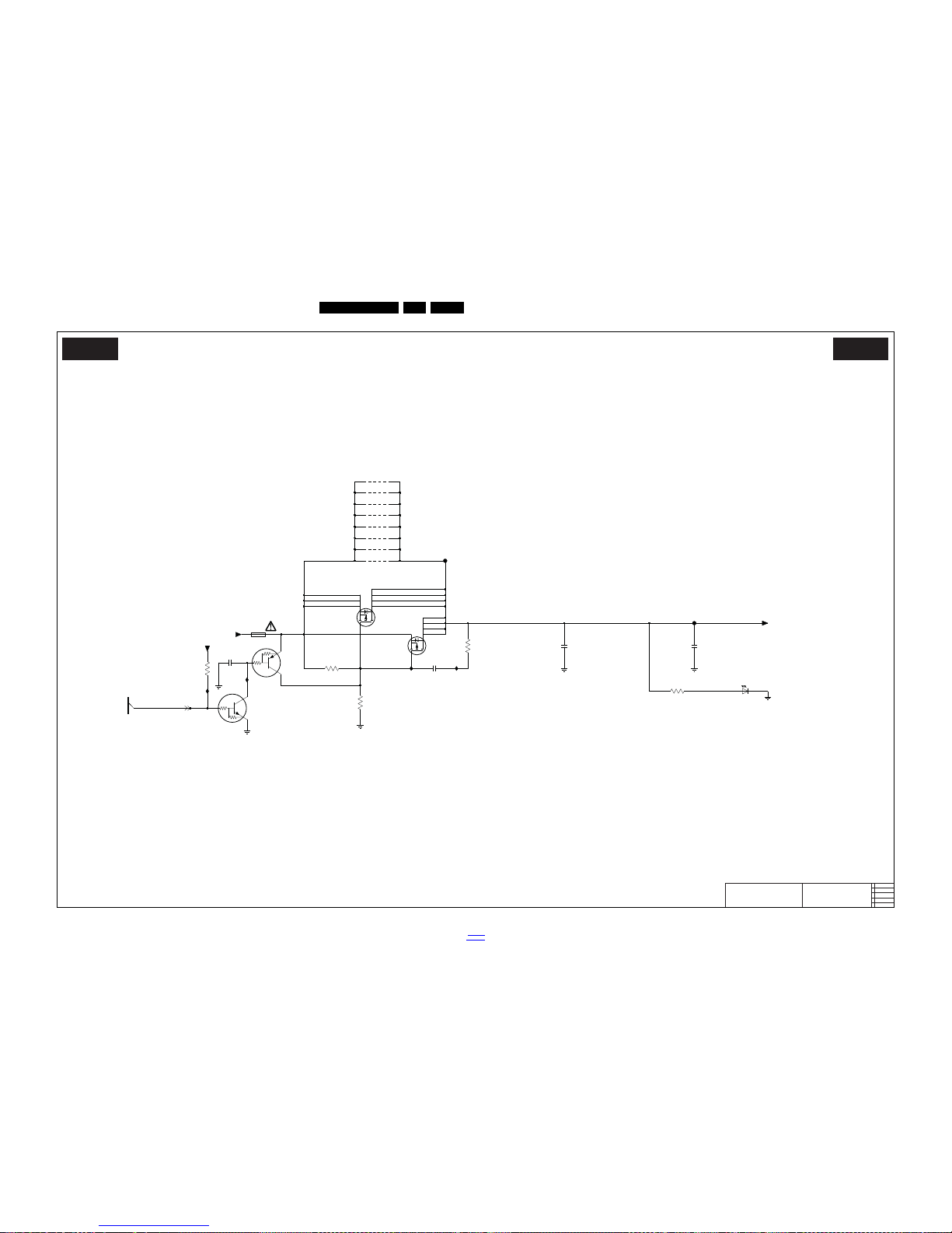
EN 76QFU1.2E LA 10.
Circuit Diagrams and PWB Layouts
2014-Jan-10
back to
div. table
10-1-18 B04C, Output Vdisp
19370_144_130227.eps
130227
Output Vdisp
B04C B04C
2012-11-22
4
3104 313 6612
Output Vdisp
+12V
22n
2GS3
IGS5
RES
4K7
3GS3
3
+3V3
SI4835DDY-GE3
RES
5
6
7
8
4
1
2
9GS1-1
1 8
7GS1
45
RES
RES
3 6
RES
9GS2-4
RES
45
9GS2-3
9GS1-3
3 6
9GS1-4
RES
RES
IGS4
22u
2GS1
LTST-C190KGKT
6GS1
DBG
IGS1
3GS1
47R
7
2GS5
100n
9GS1-2
RES
2
T
1GS1
4.0A32V
DBG
FGS2
4K7
3GS5
5
3
4
FGS1
1
PUMD12
7GS3-2
7GS3-1
PUMD12
2
6
27K
3GS4
3GS6
6
3
4
47K
SI3443CDV
1
2
5
8
IGS2
7GS2
27
9GS2-1
RES
1
RES
9GS2-2
100n
2GS2
+VDISP
LCD-PWR-ONn
RES
Page 77
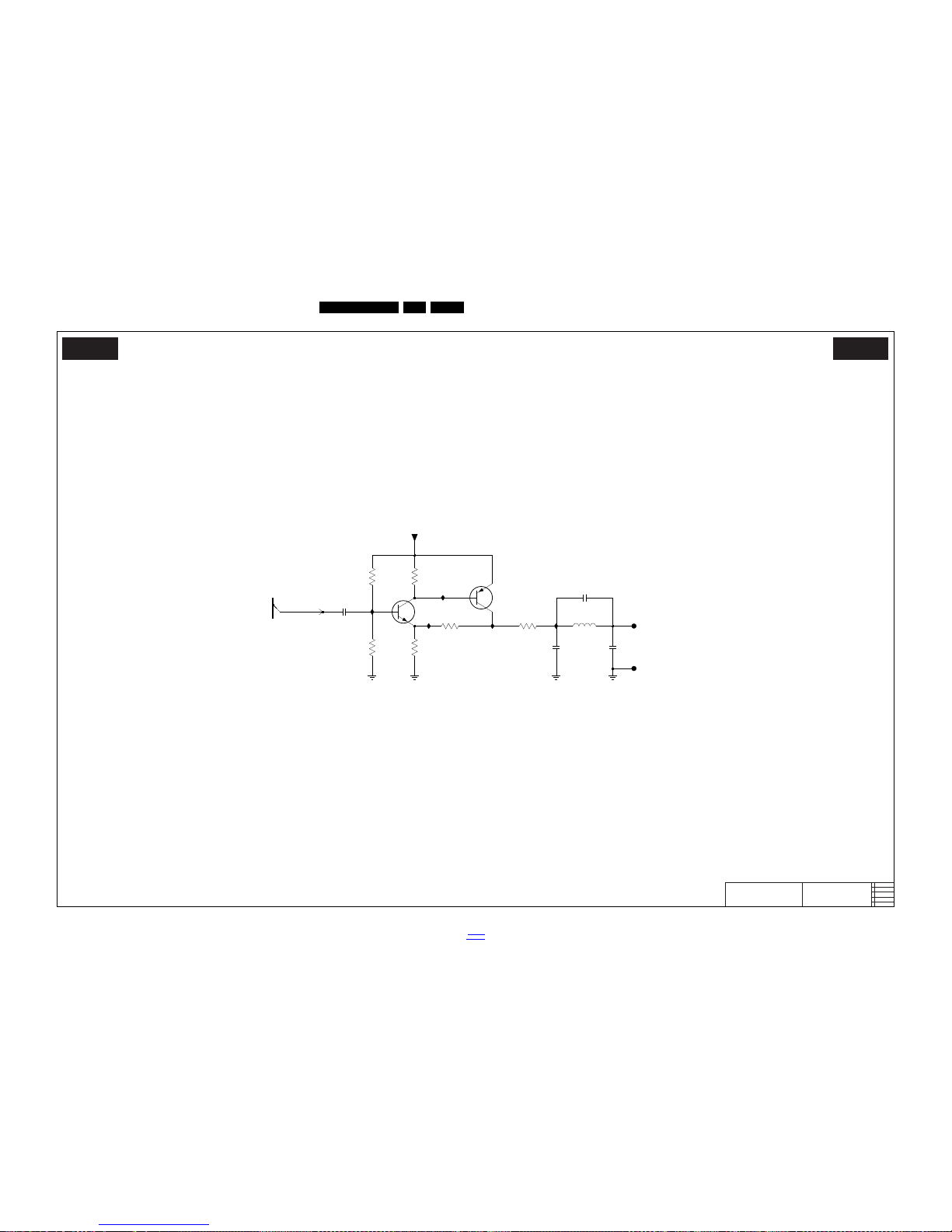
Circuit Diagrams and PWB Layouts
EN 77QFU1.2E LA 10.
2014-Jan-10
back to
div. table
10-1-19 B04D, Tuner CVBS debug
19370_145_130227.eps
130227
Tuner CVBS debug
B04D B04D
2012-11-22
4
3104 313 6612
Tuner CVBS debug
RES
33p
2FW3
100p
2FW5
RES
RESRES
5FW3
1u8
RES
3FW5
R57R051
3FW8
150R
3FW7
SERSER
+12V
470R
3FW4
BC847BPN(COL)
RES
5
3
4
RES
2
6
1
7FW1-2
RES
7FW1-1
BC847BPN(COL)
RES
3FW6
K013K3
3FW3
47u
2FW4
RES
IFW1
RES
IFW5
270p
2FW6
DFW2
DFW1
IFW2
IFW4
CVBS-OUT1
IFW3
Page 78
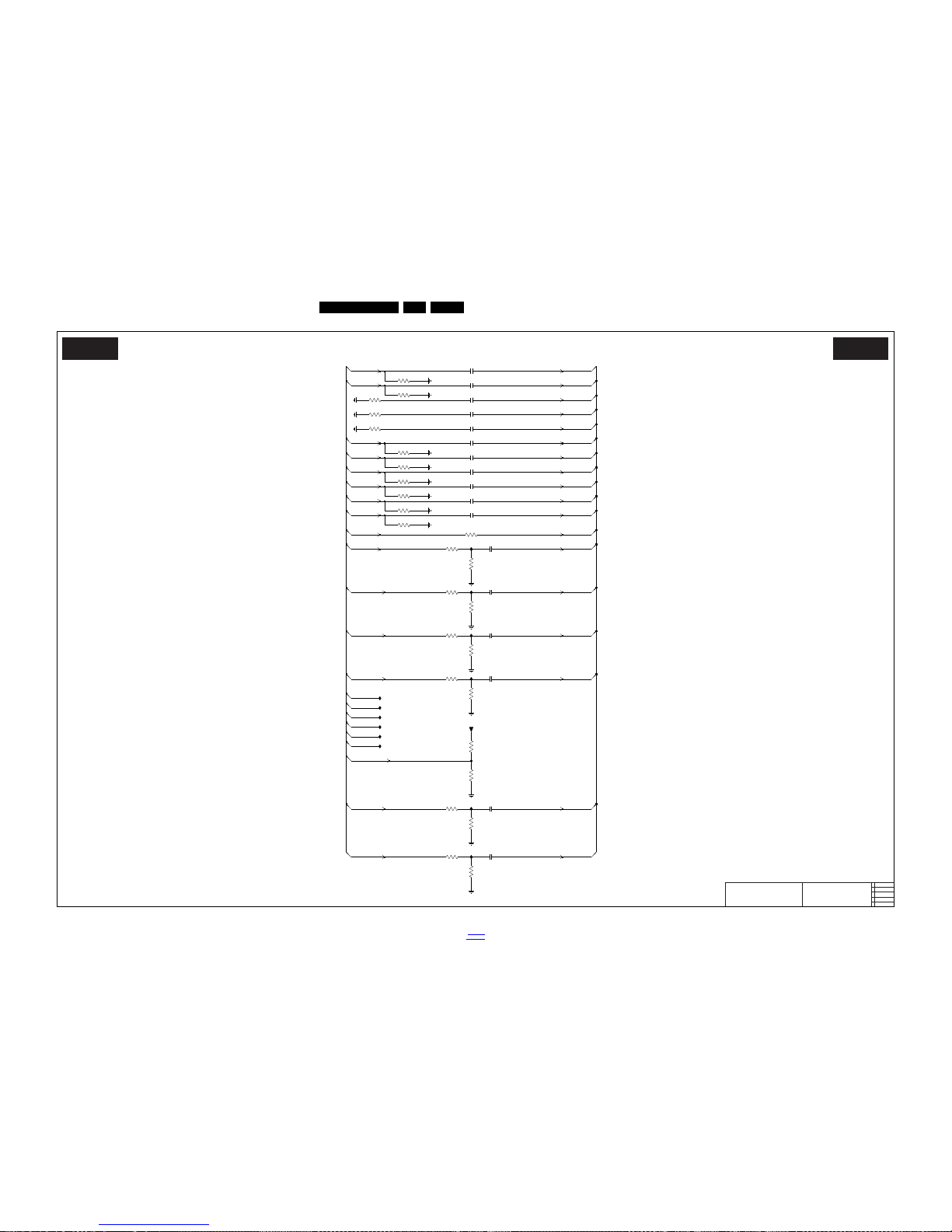
EN 78QFU1.2E LA 10.
Circuit Diagrams and PWB Layouts
2014-Jan-10
back to
div. table
10-1-20 B04E, Audio - video
19370_146_130227.eps
130227
Audio - video
B04E B04E
2012-11-22
4
3104 313 6612
Audio - video
2VW7
100n
3VW6
33K
2VW2
100n
3VWM
150R
150R
100n
2VW6
3VWS
IVW2
2VW9
100n
DVW1
IVW3
3VWA
33K
3VWW
8K2
10K
1u0
2VWC
3VWH
3VWU
150R
DVW2
RES
3VWJ
33K
IVW8
3VWD
150R
DVW4
3VW9
8K2
IVW1
150R
3VWT
2VWB
100n
3VWB
150R
33K
3VW8
8K2
3VW7
2VWD
1u0
33K
3VW4
2VW3
100n
100n
2VW8
8K2
3VW3
DVW6
100n
2VW1
IVW7
2VWF
1u0
33K
3VWL
4K7
3VWF
2VW5
100n
3VW5
8K2
1u0
2VWK
8K2
3VWK
DVW5
2VWJ
1u0
1u0
2VWE
150R
3VWV
150R
3VWC
RES
3VWG
4K7
IVW4
DVW3
100n
2VW4
150R
+3V3
3VWP
150R
3VWR
150R
3VWN
100n
2VWA
SDI2SIN
WSI2SIN
SPDIFIN
SCKIN
AUD-R
AUD-L
SC1-G
AL-4
AUDIO-MUTEn
VGA-LIN AL-3
VGA-RIN AR-3
CVBS1
SC1-B
SC1-R
SC1-BLK FB1
YPBPR-RIN AR-1
YPBPR-LIN AL-1
SC-RIN AR-4
SC-LIN
CVBS
SC1-CVBS CVBS3
Y-G1
PB-B1
PR-R1
Y1-IN Y-G2
PB1-IN PB-B2
PR1-IN PR-R2
Y-G3
PB-B3
PR-R3
Page 79
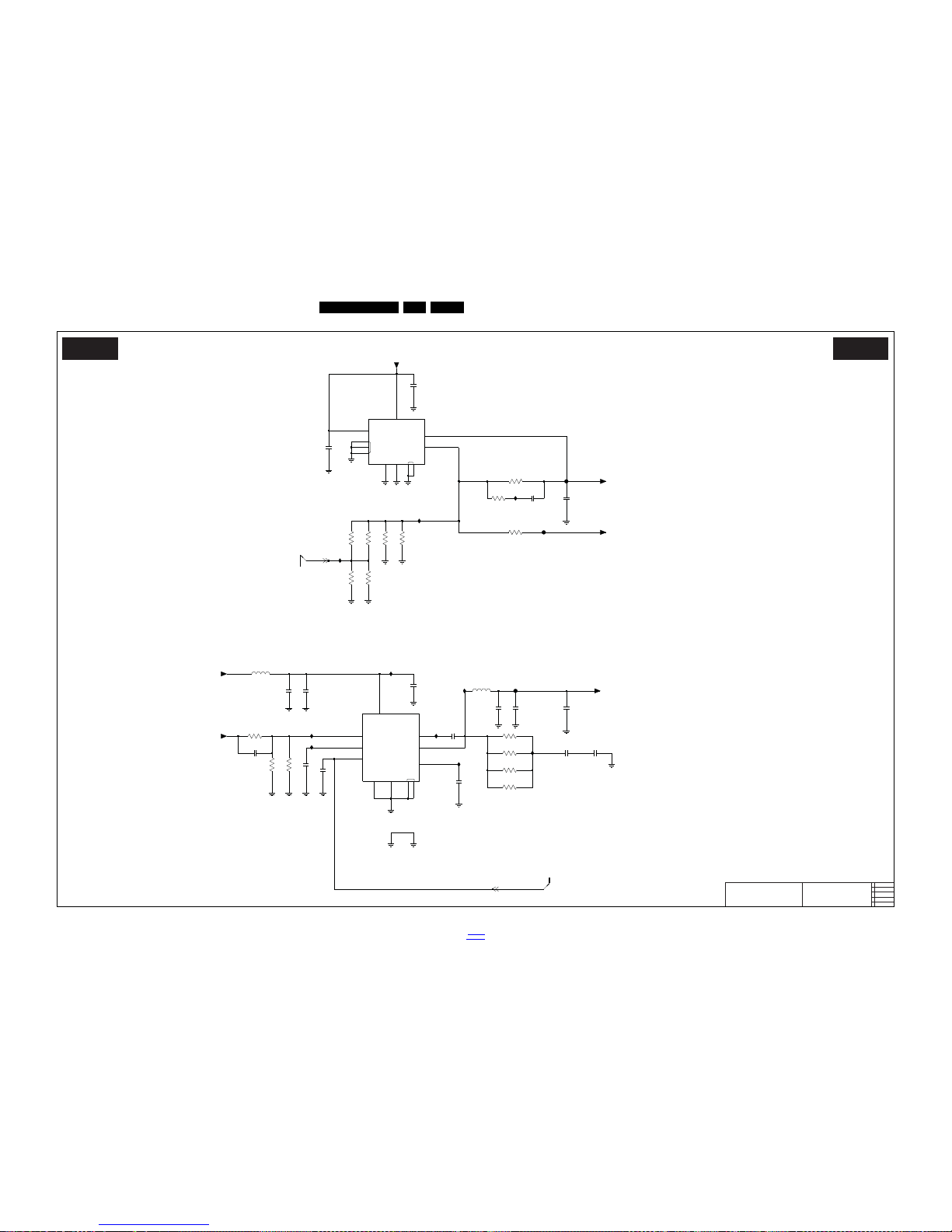
Circuit Diagrams and PWB Layouts
EN 79QFU1.2E LA 10.
2014-Jan-10
back to
div. table
10-1-21 B04F, Fusion supply
19370_147_130227.eps
130227
Fusion supply
B04F B04F
2012-11-22
4
3104 313 6612
Fusion supply
NC
VIA
EN
GND
GND_HS
IN
OUT
FB
SW
VREG5
GNDGND_HS
VFB
VIA
EN
VIN
SS
VBST
CORE VOLTAGE SUPPLY MIPS FUSION
DDR3 SUPPLY FUSION
3UBB
22K 1%
2UB6
100n
1u0
2UBF
3UB9
10K 1%
47K
3UB6RES
1%
GND-1V5
IUB4
3UB4
1K0
IUBC
CUB0
3UBD
470K
RES
5UB0
30R
3
1
4
5
6
10
11
GND-1V5
Φ
TPS7A7001DDA
7UB1
2
7
8
9
3UB7
220K
1%
2UBA
22u
10u
2UB9
3UBC
22K
1%
IUB7
GND-1V5
1%
8
+1V5
3UB8
22K
3UBE-1
10R
1
IUB6
8
3
IUBA
1
5
9
46
72
10
11
STEP DOWN
Φ
TPS54527DDA
7UB5
3UBE-3
10R
3 6
2UB0
10u
2UB8
10u
IUB3
10n
2UBG
100p
2UB3
FUB2
RES
2UBB
22u
2UB4
100n
2UBD
10u
RES
22p
2UBE
+1V2-MIPS
1n0
2UBH
RES
3UBA
1M0
SENSE+1V2-MIPS
+1V5
3UBF
12K
1%
IUB5
2u0
5UB1
2UBC
22u
+12Va
RES
FUB1
3UB3
27K 1%
27
GND-1V5
2UBJ
1n0
10R
3UBE-2
FUB0
IUBB
IUB8
+1V5
10R
3UBE-4
45
100n
2UB7
1%100K
3UB5
1n0
2UBK
GND-1V5
IUB9
DVS2
ENABLE+1V5+1V1
Page 80
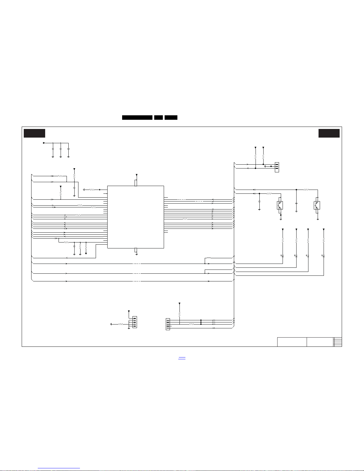
EN 80QFU1.2E LA 10.
Circuit Diagrams and PWB Layouts
2014-Jan-10
back to
div. table
10-1-22 B04G, Backlight microcontroller
19370_148_130227.eps
130227
Backlight microcontroller
B04G B04G
2012-11-22
4
3104 313 6612
Backlight microcontroller
VSS
VDD
XTALIN
XTALOUT
+3V3
1u0
2GE6
100n
2GE1
FGE6
9GE2
4K7
3GE1
5
41
6
7
36
PIO3_0|DTR_|CT16B0_MAT0|TXD
37
PIO3_1|DSR_|CT16B0_MAT1|RXD
43
PIO3_2|DCD_|CT16B0_MAT2|SCK1
48
PIO3_3|RI_|CT16B0_CAP0
18
PIO3_4|CT16B0_CAP1|RXD
21
PIO3_5|CT16B1_CAP1|TXD
8
44
38
PIO2_3|RI_|MOSI1
19
PIO2_4|CT16B1_MAT1|SSEL1
20
PIO2_5|CT32B0_MAT0
1
PIO2_6|CT32B0_MAT1
11
PIO2_7|CT32B0_MAT2|RXD
12
PIO2_8|CT32B0_MAT3|TXD
24
PIO2_9|CT32B0_CAP0
47
PIO1_7|TXD|CT32B0_MAT1
9
PIO1_8|CT16B1_CAP0
17
PIO1_9|CT16B1_MAT0|MOSI1
2
PIO2_0|DTR_|SSEL1
25
PIO2_10
31
PIO2_11|SCK0|CT32B0_CAP1
13
PIO2_1|DSR_|SCK1
26
PIO2_2|DCD_|MISO1
30
PIO1_10|AD6|CT16B1_MAT1|MISO1
42
PIO1_11|AD7|CT32B1_CAP1
34
PIO1_1|R|AD2|CT32B1_MAT0
35
PIO1_2|R|AD3|CT32B1_MAT1
39
PIO1_3|SWDIO|AD4|CT32B1_MAT2
40
PIO1_4|AD5|CT32B1_MAT3|WAKEUP
45
PIO1_5|RTS_|CT32B0_CAP0
46
PIO1_6|RXD|CT32B0_MAT0
14
PIO0_3
15
PIO0_4|SCL
16
PIO0_5|SDA
22
PIO0_6|SCK0
23
PIO0_7|CTS_
27
PIO0_8|MISO0|CT16B0_MAT0
28
PIO0_9|MOSI0|CT16B0_MAT
33
PIO1_0|R|AD1|CT32B1_CAP0
LPC1114FBD48/301
7GE0
3
PIO0_0|RESET_
29
PIO0_10|SWCLK|SCK0|CT16B0_MAT2
32
PIO0_11|R|AD0|CT32B0_MAT3
4
PIO0_1|CLKOUT|CT32B0_MAT2
10
PIO0_2|SSEL0|CT16B0_CAP0
FGE0
DBG
LTST-C190KGKT
6GE2
RES
9GE0
3GEJ
1K0
3GE6
1K0
RES
RES
+3V3
100R
3GEK
2GE2
100n
RES
3GEH
100R
1K0
3GE2
RES
FGE5
+3V3
10R
3GEA
RES
RES
+3V3
100n
2GE3
3GEE
330R
DBG
3GE3
100R
1
2
3
4
DBG
1GE2
SKHUBHE010
FGE7
2GE4
100n
DBG
FGE3
330R
3GEC
10R3GE8
FGE8
FTSH-105-01-L-DV
ROW_1
1GE3-1
1
3
5
7
9
+3V3
DEBUG
3GEM
100K
RES
RES
100K
3GEN
+3V3
+3V3
3GE0
4K7
3GE9
10R
RES
9GE1
RES
SKHUBHE010
1GE1
1
2
3
4
DBG
IGE1
+3V3
10R
3GE7
1
2
3
45
+3V3
DBG
BM03B-SRSS-TBT
1GE0
3GEG
10K
RES
2GE0
1u0
6GE3
LTST-C190KGKT
100n
2GE5
DBG
+3V3
+3V3
9GE3
DBG
3GE5
100R
cGE1
cGE2
FGE4
DBG
4
6
8
10
+3V3
6GE1
LTST-C190KGKT
DEBUG
FTSH-105-01-L-DV
ROW_2
1GE3-2
2
10K
3GEL
FGE1
+3V3
FGE2
330R
3GEF
DBG
9GE4
DBG
100R
3GE4
3GEB
330R
DBG
RESET-FUSION-OUTn
LPC-RESETn
AMBI-SPI-OUT-CCLK
AMBI-SPI-CCLK-OUT
AMBI-SPI-OUT-MOSI
AMBI-SPI-MOSI-OUT
DBG
LTST-C190KGKT
6GE0
AMBI-SPI-MOSI
LPC-LED1
LPC-ISPn
LPC-LED2
LPC-LED3
LPC-LED4
LPC-RESETn
TXD-LPC
RXD-LPC
LPC-SWDIO
LPC-SWCLK
LPC-RESETn
AMBI-SPI-OUT-MOSI
3D-LR-DISP
AMBI-SPI-OUT-CCLK
SCL-SSB
SDA-SSB
AMBI-SPI-MOSI
AMBI-SPI-CCLK
AMBI-SPI-OUT-MOSI
AMBI-SPI-CCLK
BL-DIM BL-DIM1
LPC-SWCLK
BL-DIM1
LPC-ISPn
BL-DIM2
BL-DIM7
BL-DIM3
BL-DIM4
LPC-SWDIO
BL-DIM
RXD-LPC
TXD-LPC
BL-SPI-CS_BL-I-CTRL
LPC-LED4
3D-LED_3D-RF
3D-LR
LPC-LED1
LPC-LED2
LPC-LED3
BL-DIM5
BL-DIM6
BL-DIM8
Page 81
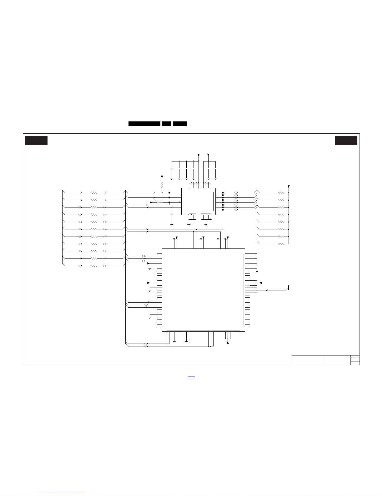
Circuit Diagrams and PWB Layouts
EN 81QFU1.2E LA 10.
2014-Jan-10
back to
div. table
10-1-23 B04H, eMMC
19370_149_130227.eps
130227
eMMC
B04H B04H
2012-11-22
4
3104 313 6612
eMMC
NC
NC
NC
NC
DATA
CMD
CLK
RST
VDDI
VSS VSSQ
VCCQ VCC
0
1
2
3
4
5
6
7
100n
2EJ6
2EJ1
100n
3 6
2EJ4
100n
+3V3
47K
3EJ3-3
C2
C4N2N5
P4
P6
G5
E7
K8
H10
B6
K5
C6
M4
N4P3P5E6F5
K9
J10
M6
M5 A3
A4
A5
B2
B3
B4
B5
MAIN
H26M21001ECR
7EJ0-1
45
3EJ6-4
33R
FEJ1
M3M7M8M9M10
M11
FEJ8
K13
K14
L1
L2
L3
L12
A12
L13
L14
M1
M2
J13
J14
K1
K2
K3
A11
K6
K7
K10
K12
H3
H5
H12
H13
H14A10
J1
J2
J3
J5
J12
F14
G1
G2
G3
G10
A9
G12
G13
G14
H1
H2
E12
E13
E14
F1
A8
F2
F3
F10
F12
F13
D12
D13
D14
E1
A7
E2
E3E5E8
E9
E10
C9
C10
C11
C12
A6
C13
C14
D1D2D3
D4
B11
B12
B13
A2
B14
C1
C3
C5
C7
C8
P10
B1
P11
P12
P13
P14
B7
B8
B9
B10
A14
N11
N12
N13
N14P1P2P7P8
P9
M12
M13
M14
N1
N3N6N7N8N9
N10
A1
A13
+3V3
+3V3
NC
H26M21001ECR
7EJ0-2
FEJ7
3EJ5
33R
100n
FEJ5
2EJ2
FEJ9
FEJ4
FEJB
+3V3
3EJ7-1
33R
1 8
+3V3
+3V3
3EJ0
10K
FEJ6
100n
2EJ3
27
2EJ5
100n
3EJ7-2
33R
3EJ8
33R
3 6
FEJ2
27
3EJ2-3
47K
47K
3EJ2-2
+3V3
1 8
FEJ3
33R
3EJ6-1
2EJ7
100n
5
3EJ7-4
33R
4
33R
3EJ4
27
3EJ3-2
47K
45
+3V3
47K
3EJ2-4
+3V3
FEJ0
1 8
FEJA
3EJ2-1
47K
3EJ6-3
33R
3 6
+3V3
27
5
+3V3
33R
3EJ6-2
3EJ3-4
47K
4
47K
3EJ3-1
1 8
+3V3
4K7
3EJ1
3 6
3EJ7-3
33R
GPIO18SDIO2-D3
GPIO19 SDIO2-D2
GPIO20 SDIO2-D5
GPIO21 SDIO2-D6
GPIO22 SDIO2-D7
GPIO24 SDIO2-D4
GPIO23SDIO2-RESETn
SDIO2-CMD
SDIO2-CLK
SDIO2-D3
SDIO2-RESETn
SDIO2-D4
SDIO2-D0
SDIO2-D1
SDIO2-D2
SDIO2-D3
SDIO2-D4
SDIO2-D5
SDIO2-D6
SDIO2-D7
GPIO16 SDIO2-D0
GPIO14 SDIO2-CLK
GPIO15 SDIO2-CMD
GPIO17 SDIO2-D1
SDIO2-CLK
SDIO2-CMD SDIO2-D0
SDIO2-D1
SDIO2-D2
SDIO2-D3
SDIO2-D4
SDIO2-D5
SDIO2-D6
SDIO2-D7
SDIO2-RESETn
VDDI
VDDI
SDIO2-D4
SDIO2-D5
SDIO2-D6
SDIO2-D7
SDIO2-D5
Page 82
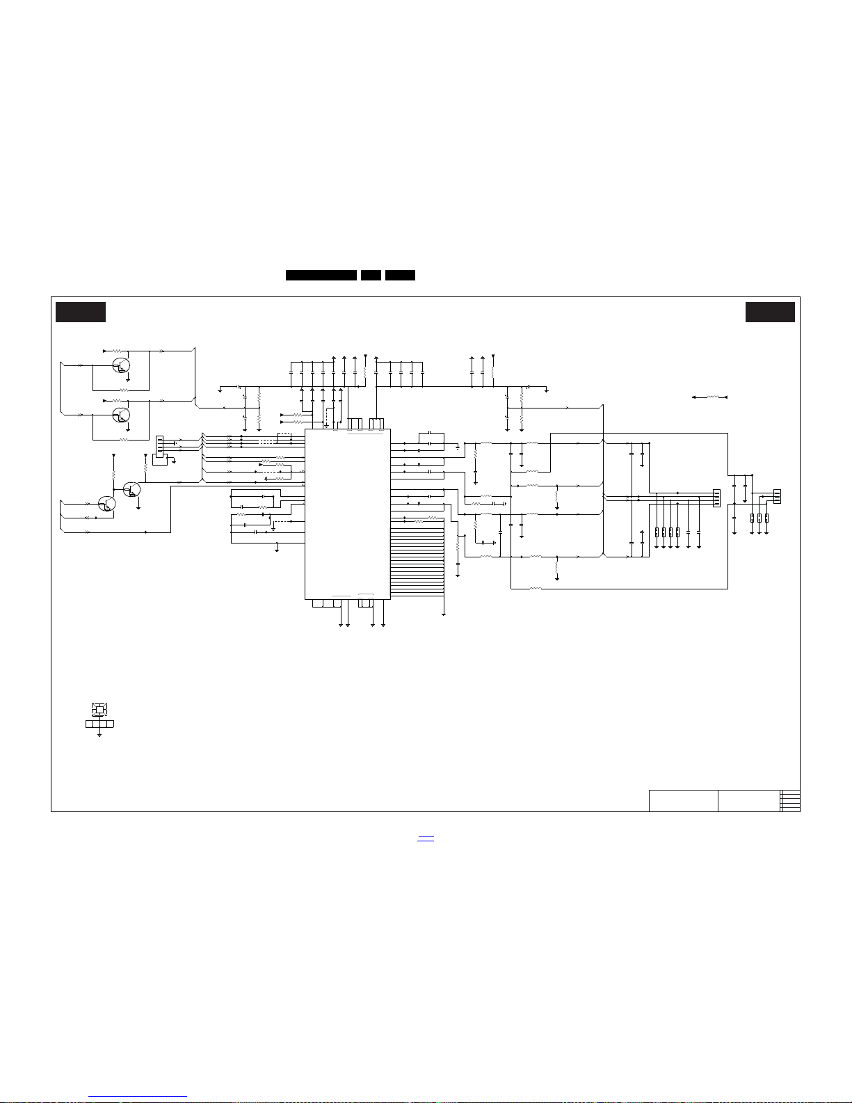
EN 82QFU1.2E LA 10.
Circuit Diagrams and PWB Layouts
2014-Jan-10
back to
div. table
10-1-24 B05A, Class-D amplifier
19370_150_130227.eps
130227
Class-D amplifier
B05A B05A
2012-11-22
4
3104 313 6612
Class-D amplifier
VR_ANA
D
PVDD
AVDD DVDD
OUT
VR_DIG
VREG
RESET
PDN
PLL_FLTP
PLL_FLTM
PBTL
SSTIMER
C
OUT_A
BST_A
BST_B
OUT_B
OUT_C
BST_C
BST_D
OUT_D
OC_ADJ
OSC_RES
VIA
ADDOGND GND_HS
STEST
AGND
LRCLK
SCLK
MCLK
SDIN
SDA
SCL
GVDD
AB CD
PGND
VSS
AB
A_SEL
LeftRight-
Left+
TAS5731P1
Right+
ID61
3D74
18R
2D60
10u
2D59
1
2
3
4
10u
1D01
2041145-4
ID87
330p
2D75
2D93
ID77
RES
1u0
3D52
470R
2D97
10u
3D54
47K
ID69
1D54
2D55
220n
1R0
33n
2D82
3D58
+3V3D
ID91
RES
1
3
2
PDTC144EU
7D71
2D91
10n
220n
2D56
3D79
+12V-AUDIO
10K
+3V3D
220n
2D61
100n
2D74
2D94
330p
2D84
10u
ID58
2D99
10n
3D61
10R
FD66
18R
3D73
220n
2D62
ID75
10n
2D73
2D78
10n
10K
3D82
10u
2D92
ID51
ID76
3D76
10K
RES
1D02
2041145-3
1
2
3
9D51
FD63
ID82
BM04B-SRSS-TBT
DBG
1
2
3
4
56
1D03
ID81
FD70
ID94
10u
2D57
4n7
2D50
9D55
RES
5D01
30R
10u
5D70
10u
47n
2D51
5D74
10K
3D50
10u
2D96
ID78
1
3
2
7D70
PDTC144EU
9D52
RES
ID52
22K
3D70
ID63
10u
2D86
ID50
2D79
33n
ID90
2D5C
100u 16V
10u
2D63
10n
2D76
ID54
16V100u
2D5A
2D48
100u16V
47R
3D56
+3V3-STANDBY
1%18K2
3D71
3D55
47R
330p
2D95
FD69
FD32
2D64
220n
5D79
10u
1D53
+3V3
30R
5D85
1D56
220n
2D71
+3V3D
1D55
30R
5D77
18
ID80
69
52
53
54
55
56
57
58
31
12
59
60
61
62
63
64
65
66
67
68
51
34
35
25
24
21
23
22
6
26
50
37
38
10
11
23444540
41
7
16
1
46
39
36
8
19
47
48
42
33
27
281729
49
5
32
20
15
30 13
9
14
4
43
10u
2D72
TAS5711PHP
7D60
AUDIO
AMPLIFIER
2D65
220n
2D77
100n
2D52
47n
3D60
10K
+12V-AUDIO
15K
3D77
ID66
PUMH2
10n
2D81
7D50-2
ID79
2D5B
100u 16V
2D83
220n
3D78
10K
2D89
220n
2D53
4n7
2D70
10n
ID70
ID98
9D53
RES
3D83
10K
FD67
ID57
ID89
30R
5D81
FD31
5D71
30R
30R
5D75
ID93
10n
2D87
10R
3D63
RES
16V100u
2D49
1D50
+3V3D
+3V3D
ID65
REF EMC HOLE
1X02
2n2
2D54
ID83
FD33
1u0
2D67
33n
2D85
18R
3D75
1D51
ID56
2D58
10u
FD64
10u
5D76
16V100u
2D5D
30R
5D50
ID55
ID62
2D98
10n
ID84
2D88
330p
PUMH2
7D50-1
100n
2D69
1D52
+3V3D
10K
3D62
CD00
1R0
3D57
ID96
ID53
5D80
30R
100n
2D68
ID97
3D72
18R
5D83
30R
ID88
+3V3D
3D51
470R
5D00
30R
ID99
5D51
30R
FD65
2D80
33n
FD50
FD30
9D54
2D66
10u
RES
SPEAKER-L+
SDI2SOUT1
SCKI2SOUT
WSI2SOUT
9D50
SPEAKER-R-SPEAKER-L-
SPEAKER-L+
SPEAKER-L-
SPEAKER-R+
SPEAKER-R-
SPEAKER-R+
SPEAKER-L-
AUDIO-MUTE
DETECT12V
A-STBY
SDI2SOUT3
A-STBY
AUDIO-MUTE
AUDIO-MUTEn
D-RESET
I2SCLK
SCKI2SOUT
RESET-FUSION-OUTn
D-RESET
SPEAKER-R-
SCL-SSB
SDA-SSB
SDI2SOUT1
WSI2SOUT
Page 83
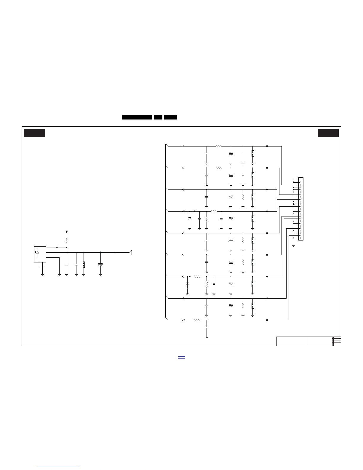
Circuit Diagrams and PWB Layouts
EN 83QFU1.2E LA 10.
2014-Jan-10
back to
div. table
10-1-25 B05B, Analogue externals
19370_151_130227.eps
130227
Analogue externals
B05B B05B
2012-11-22
4
3104 313 6612
Analogue externals
MT
SCART
RES
2D0A
100n
2D0B
100p
6VAE
RES
12V
CDS4C12GTA
3
GND
45
2
VCC
1
VIN
3150-831-030-H1
1J50
ID95
1VAM
RES
6VAG
CDS4C12GTA
12V
6VA9
RES
3VA9
12K
12V
CDS4C12GTA
1VAJ
FVAF
FVAC
RES
6VAA
CDS4C12GTA
12V
2VAB
6n8
3VAE
75R
2VAF
100p
1VAK
75R
3VAC
FVAB
6VAB
PDZ2.4B(COL)
RES
6VA8
CDS4C12GTA
12V
1K0
3VA8
4
5
6
7
8
9
25 26
2VAA
100p
16
17
18
19
2
20
21
22
23
24
3
1
10
11
12
13
14
15
49045-0011
1VA1
FVA2
1VAP
100p
2VAC
FVA1
1u0
2VAD
6VAF
PDZ2.4B(COL)
1VAH
100p
2VAG
1VAN
RES
6VAD
CDS4C12GTA
12V
IVA1
FD90
2VAK
100p
3VAD
100R
3VAK
47R
12V
CDS4C12GTA
6VAC
RES
FVAE
V_NOM
1D0A
75R
3VAG3VAF
150R
1VAL
2VAE
100p
FVAG
FVA4
1R0
3D90
+3V3
FVAD
100p
FVAA
IVA0
2VAH
3VA7
1K0
100p
2VA8
FVA9
12V
CDS4C12GTA
6VAH
RES
12V
CDS4C12GTA
6D0A
RES
2VAJ
100p
6n8
2VA9
3VAA
1K5
1VAG
3VAB
75R
SC1-STATUS
SPDIFO
SC1-R
SC1-CVBS
SC1-DETECTn
SC1-BLK
SC-RIN
SC-LIN
SC1-B
SC1-G
Page 84
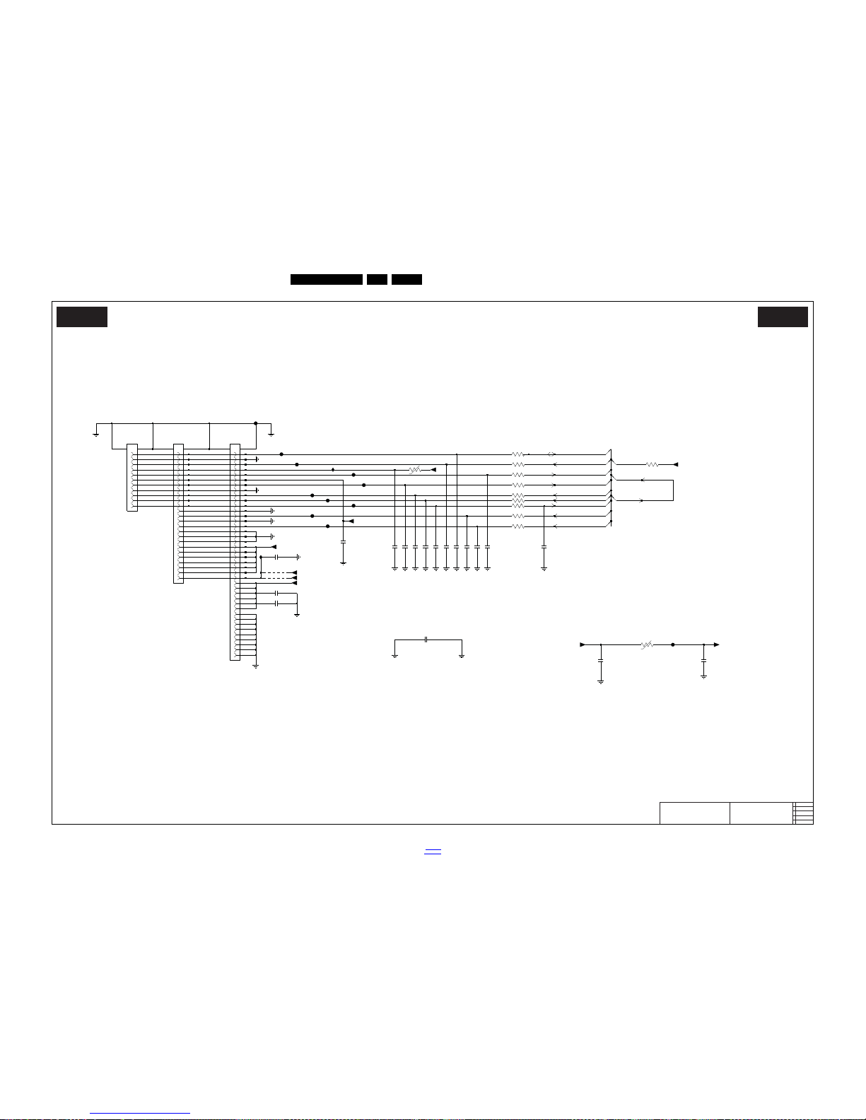
EN 84QFU1.2E LA 10.
Circuit Diagrams and PWB Layouts
2014-Jan-10
back to
div. table
10-1-26 B05C, Sensor board and AmbiLight
19370_152_130227.eps
130227
Sensor board and AmbiLight
B05C B05C
2012-11-22
4
3104 313 6612
Sensor board and AmbiLight
+T
+T
9CAA
FAA4
2AAC
470p
IAA0
FAA9
1u0
FAA7
FAA2
2CAS
FAA1
3CAH
10K
1u0
2AAW
GND-AL
3CAF
10R
GND-AL
10R
3CAE
10p
2CAB
100p
2CAP
AMBI-POWER
2CAR
100p
2CAN
100p
FAA0
FAA8
IAA1
3CAB
100R
GND-AL
AMBI-POWER
+3V3
RES
2CAA
10p
10u
2CAU
100n
2CAT
GND-AL
+3V3-STANDBY
3AAA
100R
FAA3
3AAC
47R
AMBI-POWER
3CAG
0R3
+5V
10p
9CAB
13
GND-AL
2CAD
10
11
2
3
4
5
6
7
8
9
12
1C20
FH52-11S-0.5SH
1
2CAL
RES
100n
10u
2AAD
GND-AL
10R
3CAD
FAA5
1u0
2CAJ
+3V3AL
+3V3-STANDBY
FAAZ
100p
2CAM
3CAC
10R
3CAA
100R
8
9
4142
34
35
36
37
38
39
4
40
5
6
7
25
26
27
28
29
3
30
31
32
33
15
16
17
18
19
2
20
21
22
23
24
1
10
11
12
13
14
6
7
8
9
2627
1C26
FH52-40S-0.5SH
2
20
21
22
23
24
25
3
4
5
1
10
11
12
13
14
15
16
17
18
19
FH52-25S-0.5SH
1C25
470p
2AAV
47R
3AAB
2AAE
10u
FAA6
+3V3AL
2CAK
1u0
0R3
3AAD
SCL-SRF
SDA-SRF
LED2-OUT
AMBI-TEMP
RC_IRQ-RF4CEn
AMBI-SPI-MOSI-OUT
AMBI-SPI-CCLK-OUT
KEYBOARD_IRQ-SRFn
LED2-OUT
LED2-OUT
SDA-MC3D-LED_3D-RF
Page 85
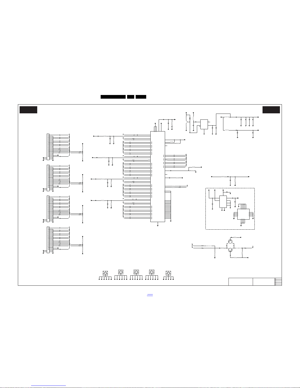
Circuit Diagrams and PWB Layouts
EN 85QFU1.2E LA 10.
2014-Jan-10
back to
div. table
10-1-27 B06A, HDMI
19370_153_130227.eps
130227
HDMI
B06A B06A
2012-11-22
4
3104 313 6612
HDMI
ADJ
VOUT
NC
EN
VIN
HSGND
GND
VDD
PGOOD
VIA
VIA
VIA
VIA
VIN
VOUT
GND
EN
FLG
EN
CEC_A
(CBUS) HPD2
R2PWR5V
DSDA2
DSCL2
DSCL3
DSDA3
R3PWR5V
(CBUS) HPD3
(CBUS) HPD0
R0PWR5V
DSDA0
DSCL0
N
P
DSCL1
DSDA1
R1PWR5V
(CBUS) HPD1
VCC33
SBVCC33
MICOM_VCC33
EPAD
R3XC
N
P
R3X0
N
P
R3X1
N
P
R3X2
TX2
N
P
TX1
N
P
TX0
N
P
TXC
VIA
R4PWR5V
DSCL4
DSDA4
CEC_D
N
P
TPWR_CI2CA
RSVDL
CSDA
CSCL
INT
N
P
R0X1
N
P
R0X2
N
P
R1XC
N
P
R1X0
N
P
R1X1
N
P
R1X2
N
P
R2XC
N
P
R2X0
N
P
R2X1
N
P
R2X2
N
P
R0XC
N
P
R0X0
1V2 DVB-T2 and DVB-S2
HDMI CONNECTOR 4
SII9287B=OXB2
HDMI CONNECTOR 2
HDMI CONNECTOR 1
HDMI CONNECTOR 3
I2C ADDRESS
pin (38)
pin (49)
pins (9,27,64)
PDZ2.4B(COL)
6HA1
FHA7
SBVCC33
100K
3HAR
FHB6
FHAN
72
8
9
5
1
4
63
RT9025-12GSP
7HA1-1
FHAG
AIN-5V
5
6
7
8
9
2021
2223
13
14
15
16
17
18
19
2
3
4
1H01
1
10
11
12
3HAA-1
1 8
47K
FHB0
9HA0
FHAP
RES 2HAK
10u
FHB9
3HA3
10R
IHB4
+5V
FHA3
FHB1
FHA4
2HAG
RES
100n
BC847BW
RES
7HA2
100n
2HAL
25
26
11
12
13
141516
17
18
7HA1-2
10
19
20
21
222324
RT9025-12GSP
AIN-5V
3HB4
FHAM
22K
8
9
2021
2223
15
16
17
18
19
2
3
4
5
6
7
1
10
11
12
13
14
1H02
100K
27
3HA1-2
2HAA
10u
MICOM-VCC33
CIN-5V
2HAJ
10u
47K
3HAB-1
1 8
BIN-5V
1u0
2HAB
54
47K
3HAB-4
+3V3-STANDBY
FHA6
FHAV
VCC33
BIN-5V
EMC HOLE
1X07
72
47K
3HAA-2
FHAF
1M0
3HAL
3HA4
RES
AIN-5V
10R
R4PWR5V
FHBA
DIN-5V
+1V2-FE
100K
3 6
+3V3
3HA1-3
FHAL
FHB2
3HAA-3
3 6
47K
IHB2
2HA9
10u
3HBQ
10K
47K
3HAB-2
72
7HA3
BC847BW
1u0
2HA2
5HA5
30R
RES
VCC33
CIN-5V
4
5
6
7
8
9
2021
2223
11
12
13
14
15
16
17
18
19
2
3
1H04
1
10
2HAM
100n
47R3HAW
+5V
FHB4
CIN-5V
3HB1
RES
4K7
+3V3
100R
MICOM-VCC33
3HB3
4
3
2
5
1
7HA5
RT9715EGB
+3V3-STANDBY
+5V
FHAH
IHB3
CIN-5V
4
DIN-5V
IHB0
47K
3HAA-4
5
2HA5
1u0
3HAS
10R
10R
3HA2
FHAE
100n
IHB5
2HAN
1u0
3HA1-1
1 8
2HB4
100K
100n
2HAP
RES
3HAY
FHAS
4K7
BIN-5V
BIN-5V
3HA0
10R
+3V3
2HAD
1u0
2HA4
1u0
6
7
8
9
2021
2223
13
14
15
16
17
18
19
2
3
4
5
1
10
11
12
1H03
1X09
EMC HOLE
1X01
REF EMC HOLE
IHB1
FHAR
1u0
2HB5
REF EMC HOLE
1X14
FHAW
+3V3
1X08
EMC HOLE
FHBC
DIN-5V
3 6
IHB6
47K
3HAB-3
3HBS
27K
47R3HAV
FHAY
10K
3HBP
30R
5HA9
2K2
5
3HA6
100K
3HA1-4
4
3K3
RES
3HA5
RES
1u0
2HA1
2HAF
10u
75
76
77
78
79
80
81
82
AIN-5V
27
64
74
83
84
85
86
87
88
89
38
55
61
60
59
58
57
56
63
62
9
21
22
23
24
25
26
19
20
49
10
28
42
13
14
15
16
17
18
11
12
46
65
66
36
3
4
5
6
7
8
1
2
73
52
37
32
67
68
69
70
71
72
53
30
34
40
44
48
29
33
39
43
47
7HA0
SII9287B
31
35
41
45
50
51
54
10K
DIN-5V
3HAP
SBVCC33
FHB8
FHB5
+1V5
22K
3HB2
RES
RES
5HA6
30R
3HB0
4K7
R4PWR5V
9HA1
FHB7
FHA8
DRX-HOTPLUG
HDMIF-RXC-
PCEC-QHDMI
PCEC-HDMI
CRX2CRX2+
CRXCCRXC+
DDRX0DDRX0+
DDRX1DDRX1+
DDRX2DDRX2+
DDRXCDDRXC+
ARX1+
ARX2ARX2+
ARXCARXC+
BRX0BRX0+
BRX1BRX1+
BRX2BRX2+
BRXC+
CRX0CRX0+
CRX1CRX1+
HDMIF-RX1-
HDMIF-RX0+
HDMIF-RX0-
BRXC-
BRX-DDC-SDA
ARX-HOTPLUG
BRX-HOTPLUG
CRX-HOTPLUG
ARX-DDC-SCL
BRX-DDC-SCL
CRX-DDC-SCL
DRX-DDC-SCL
ARX-DDC-SDA
CRX-DDC-SDA
DRX-DDC-SDA
ARX0ARX0+
ARX1-
HDMIF-RXC+
HDMIF-RX2+
HDMIF-RX2-
HDMIF-RX1+
DDRXC+
DDRX0-
DDRX0+
DDRX1-
DDRX1+
DDRX2-
DDRX2+
HARC0
CRX1-
CRX1+
CRX2-
CRX-HOTPLUG
CRX-DDC-SDA
CRX-DDC-SCL
PCEC-HDMI
CRXC-
CRXC+
CRX2+
DRX-DDC-SDA
DRX-DDC-SCL
DRX-HOTPLUG
DRX-DDC-SDA
DRX-DDC-SCL
PCEC-HDMI
DDRXC-
BRX-DDC-SDA
BRX-DDC-SCL
BRX0-
BRX0+
BRX1-
BRX1+
BRX2-
BRX-HOTPLUG
BRX-DDC-SDA
PCEC-HDMI
BRXC-
BRXC+
BRX2+
CRX-DDC-SDA
CRX-DDC-SCL
CRX0-
CRX0+
ARX-DDC-SDA
ARX-DDC-SCL
ARX0-
ARX0+
ARX1-
ARX1+
ARX2-
ARX-HOTPLUG
ARX-DDC-SDA
ARX-DDC-SCL
PCEC-HDMI
ARXC-
ARXC+
ARX2+
BRX-DDC-SCL
HARC1
HARC2
SCL-SSB
SDA-SSB
HARC4
HDMI-CEC
Page 86
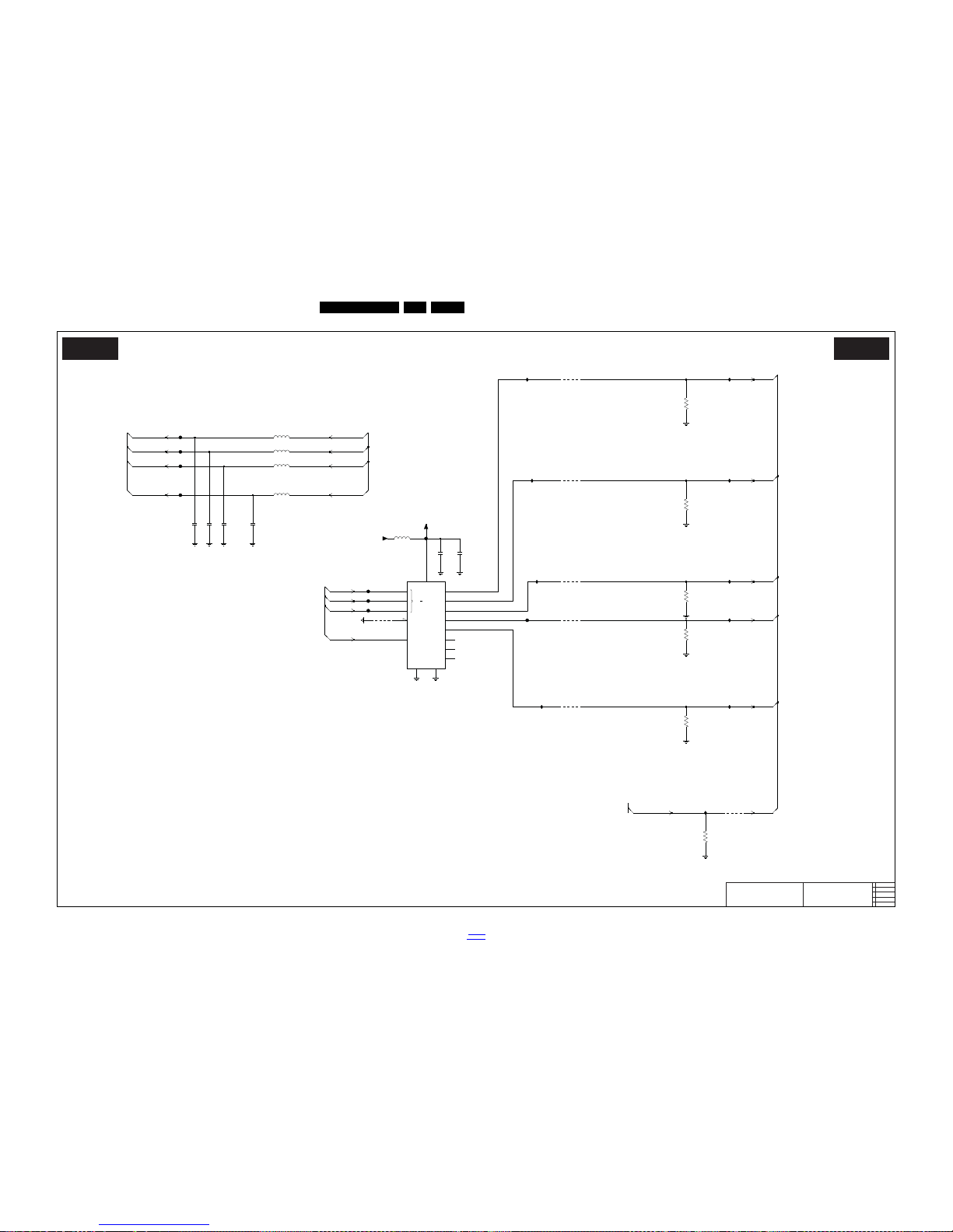
EN 86QFU1.2E LA 10.
Circuit Diagrams and PWB Layouts
2014-Jan-10
back to
div. table
10-1-28 B06B, HDMI-ARC
19370_154_130227.eps
130227
HDMI-ARC
B06B B06B
2012-11-22
4
3104 313 6612
HDMI-ARC
G8
7
8X
0
2
0
VCC
2
3
0
1
5
4
7
6
GNDVEE
IHDK
10p
2HD0
FHD3
9HD5
9HD2
IHDL
RES
100R
3HDS
100R
3HDU
9HD99HD0
IHD1
IHDG
IHDH
10p
2HD5
2HD3
10p
30R
5HD4
3HDE
100R
FHD1
IHDM
1u0
2HD6
IHDF
100R
3HDT
RES
FHD5
+5V
FHD7
1
5
2
4
3
11
10
9
16
7
13
14
15
12
74HC4051PW
7HD0
MDX
6
8
100R
3HD9
+5V-ARC
9HD8
30R
5HD5
30R
5HD2
IHD4
9HD6
3HD4
100R
FHD6
9HD4
FHD2
FHD4
IHD8
IHD7
5HD1
30R
FHD0
2HD1
10p
100n
2HDD
30R
5HD0
ARC-SEL2
ARC0
ARC1
ARC2
ARC4
ARC3
FHD8
ARC4
HDMI-ARC
ARC-SEL0
ARC-SEL1
HDMI-ARC
ARC0
HARC1
HARC2
HARC4
HARC0
ARC1
ARC2
ARC4
Page 87
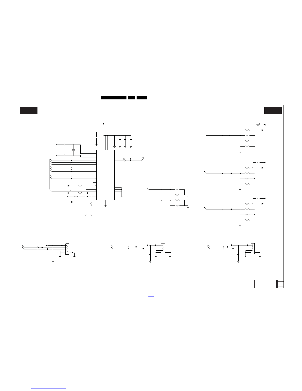
Circuit Diagrams and PWB Layouts
EN 87QFU1.2E LA 10.
2014-Jan-10
back to
div. table
10-1-29 B06C, USB external
19370_155_130227.eps
130227
USB external
B06C B06C
2012-11-22
4
3104 313 6612
USB external
+T
VCC_A_3
VCC_D
XIN
XOUT
DD1DD1+
OVR1
DD2-
VIA3
VIA4
VCC
VCC_A_1
VCC_A_2
DD2+
OVR2
DD3DD3+
OVR3
DD4DD4+
OVR4
VREG
RESET
SELFPWR
GANG
RREF
GND_HS
TEST|SCL
SDA
D-
D+
VIA1
VIA2
+T
+T
FEA9
6
FEAB
+3V3
5401
1E03
1
2
3
4
5
2EA0
18p
3EA8-2
100K
100n
2EAA
3EA1
10K
FEAH
FEA5
IEE0
12M
1EA0
3EA7
+3V3
33
28
10
11
0R3
26
22
18
27591421
30
31
32
1
2
23
29
25
24
20
19
17
8
3
4
6
7
12
13
15
16
7EA0
CY7C65632-28LTXCT
3EA5
100K
+5V-PORTA
FEA4
2EA3
100n
2EA4
100n
100n
2EA2
+3V3
100K
3EA8-1
3EA3
10K
+5V-PORTC
3EAG
0R3
+5V-PORTC
FEA8
3EA8-4
100K
+5V
4
56
1
2
3
+5V
1E02
5401
3EAH-4
100K
+5V
FEAE
FEAC FEA7
+5V-PORTA
FEA6
3EAD-1
100K
100K
3EAH-3
3EA4
680R
IEA2
100n
2EAB
IEA1
3EAH-2
100K
IEA3
100K
3EAH-1
100K
+3V3
3EA8-3
IEA4
1%
27
100n
2EA5
12K
3EE2-2
FEA1
100n
2EA7
1%
12K
3EE2-4
45
FEA3
1%
3 6
3EE2-3
12K
2EA6
100n
4
56
100K
3EAD-2
5401
1
2
3
3EE2-1
12K
1 8
1E01
1%
3EAD-3
100K
0R3
3EAC
+5V-PORTB
FEAA
18p
2EA1
2EA9
100n
+5V-PORTB
100K
3EAD-4
FEAD
IEE1
USB-PORTC-OC
FEA2
USB1-RREF
USB2-RREF
USB-PORTC-DM
USB-PORTC-DP
USB-PORTA-DM
USB-PORTA-DP
USB-PORTA-OC
USB-PORTB-OC
USB-PORTA-OC
RESET-FUSION-OUTn
USB-PORTB-DM
USB-PORTB-DP
USB-PORTB-DM
USB-PORTB-DP
USB-PORTA-DM
USB-PORTA-DP
USB2-DM
USB2-DP
USB-PORTC-DM
USB-PORTC-DP
USB-PORTC-OC
USB-PORTB-OC
Page 88
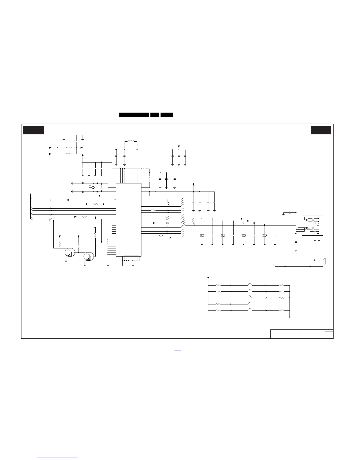
EN 88QFU1.2E LA 10.
Circuit Diagrams and PWB Layouts
2014-Jan-10
back to
div. table
10-1-30 B06D, Ethernet
19370_156_130227.eps
130227
Ethernet
B06D B06D
2012-11-22
4
3104 313 6612
Ethernet
TX+
TX-
RX+
RX-
VIA
VDDH_REG
VDDIO_REG
TRXP0
TRXN0
TRXP1
TRXN1
CLK_RMII
CRS_DV
LX
RXD0
RXD1
RX_ER
TX_EN
TXD0
XTLI
XTLO
CLK_25M
RST
RBBIAS
RES0
RES1
AVDDL
VIA
MDIO
INT
NC
MDC
GND_HS
TXD1
LED_ACT
LED_RES
LED_10_100
DVDDL
VDD33
AVDD33
16V
CDA5C16GTH
6EF2-3
RES
36
2EFL
RES
VDDH-2V5
VDDH-2V5
15p
2EFC
22p
2EF9
10u
10u
2EF2
2EF3
100n
FEF8
FEFE
FEFD
1u0
2EFF
VDDH-2V5
+3V3-STANDBY
IEF2
AVDDL-1V1
IEF3
1%
1K5
3EF3
8
2EF8
100n
1E00
5450-327-194-H3
1
2
3
4
5
6
7
1M0
3EFY
100n
2EFA
FEF7
3EFN
FEFA
5EF4
10K
30R
10n
2EFT
3EFM
10K
3EFU
10K
8
3EFL
10K
RES
16V
CDA5C16GTH
6EF2-1
1
FEF6
+3V3-LAN
FEF9
RES
15p
2EFK
100n
2EFZ
2EFS
10n
FEF0
3EFS
10K
RES
30R
5EF0
15p
RES
2EFN
100n
2EF7
22p
2EFB
FEF3
100n
2EFH
25M
1EF0
22u
2EFV
10K
3EFR
16V
45
2EFP
100n
10K
3EF4
RES
6EF2-4
CDA5C16GTH
1%
2K37
3EF2
5EF5
30R
3EFH
10K
RES
2EF0
1u0
15p
2EFM
IEF1
FEF4
3EFP
10K
FEFC
22R
3EF5
2EFU
100n
VDD33-PHY
3EFJ
10K
100n
2EF1
4u7
5EF1
50
5
4
2EFJ
100n
56
57
58
43444546474849
34
35
32
3
8
27
42
51
52
53
54
55
26
31
1
29
28
25
10
13
9
12
22
2
40
39
15
16
18
19
36
37
7
11
17
23
33
30
38
41
20
24
21
7EF0
AR8030-AL1A-R
14
6
6
1
DEF0
4
7EF1-1
PUMH2
2
7EF1-2
PUMH2
5
3
VDD33-PHY
VDD33-PHY
10K
3EFT
16V
RES
6EF2-2
27
RES
CDA5C16GTH
100n
2EF5
FEFB
FEF2
FEF1
30R
5EF6
VDD33-PHY
VDD33-PHY
FEF5
2EFG
1u0
2EF6
100n
TXP
TXN
RXP
RXN
IRQ-WOLANn
EN-RXC
LED-ACT
RESET-ETHERNETn
RES0
RES1
LED-RES
LED-ACT
EN-RXD0
EN-RXD1
EN-RXEN
RX-ER
LED-RES
EN-RXD0
EN-RXD1
RX-ER
TXN
RXN
TXP
RXP
EN-TXD0
EN-TXD1
EN-TXEN
EN-MDC
EN-MDIO
RES0
RES1 CLK-RMII
CLK-RMII
EN-TXC
EN-RXEN
Page 89
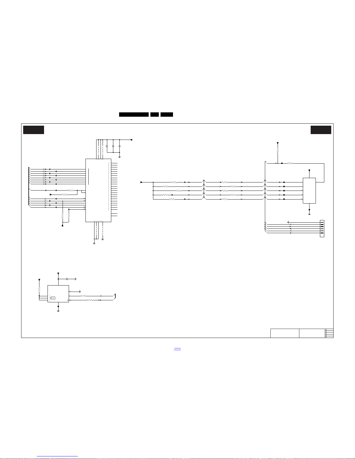
Circuit Diagrams and PWB Layouts
EN 89QFU1.2E LA 10.
2014-Jan-10
back to
div. table
10-1-31 B06E, NAND flash, serial flash and EEPROM
19370_157_130227.eps
130227
NAND flash, serial flash and EEPROM
B06E B06E
2012-11-22
4
3104 313 6612
NAND flash, serial flash
and EEPROM
SCL
ADR
0
1
2 SDA
WC
D
C
S
W
HOLD
VSS
Q
VCC
VSS
B
ALE
CLE
WE
WP
1
2
3
4
5
6
7
8
9
10
11
12
13
14
15
16
17
18
19
20
21
22
23
DNU1
DNU2
0
1
2
3
4
5
6
7
R
RE
CE
NC
IO
VCC
3JA6
33R
DJA6
3CTH
47R
FJA0
FCT2
9JA4
ICT2
DJAE
FCT4
100n
2JA4
DJA4
3CT1
4K7
1
2
3
4
5
6
78
1734260-6
1CTZ
3CTU
270R
IJA0
10K
3JA4
DJA3
47R
3JA3
9JA6
FCT5
ICT3
9JA5
6
5
7
2
1
84
3
7CT3
M25P05-AVMN6
FLASH
512K
Φ
2JA2
100n
+3V3
270R
3CT0
1
2
3
6
5
84
7
M24C64-WDW6
7JA2
EEPROM
Φ
(8K × 8)
DJAC
DJAA
+3V3-STANDBY
9JA3
4K7
3CTB
IJA1
4K7
3JA0
100n
2JA0
+3V3-STANDBY
+3V3-STANDBY
ICT1
47R
3JA2
DJA9
DJA2
DJAD
+3V3
+3V3
FCT6
3CTJ
4K7
DJAB
DJA0
39
132536
48
18
19
5
6
10
11
14
8
7
123437
26
27
28
33
2
35
40
45
46
3
4
42
43
44
1
15
20
21
22
23
24
17
9
16
38
47
29
30
31
32
41
MT29F8G08ABACAWP:C
7JA0
3CTK
4K7
+3V3
10K
3JA5
DJA1
FCT3
3JA1
4K7
RES
DJA8
+3V3
47R
3CT9
3CTZ
270R
DJA7
3CT3
4K7
47R
3CT2
FCT8
FCT7
DJA5
2JA1
100n
4K7
3CTR
SF-CS
F-RDY
SFB-SCK
SFB-CS
SFB-SI
SF-SDO
RESET-STANDBYn
SF-SDI
SF-CLK
SF-WP
SF-HOLDn
SF-CS
SF-CLK
SF-HOLDn
SF-WP
SF-SDI
SFB-SI
SFB-SCK
SFB-WPn
SFB-HOLDn
SFB-CS
SFB-SCK
SFB-SI
SFB-HOLDn
SF-SDO
SFB-CS
SFB-WPn
SDA-SSB
SCL-SSB
NAND-ALE
F-CEn
NAND-CLE
FRA0
FRA5
FRA6
FRA7
FRA8
FRA10
FRA11
FRA12
F-OEn
F-WEn
Page 90
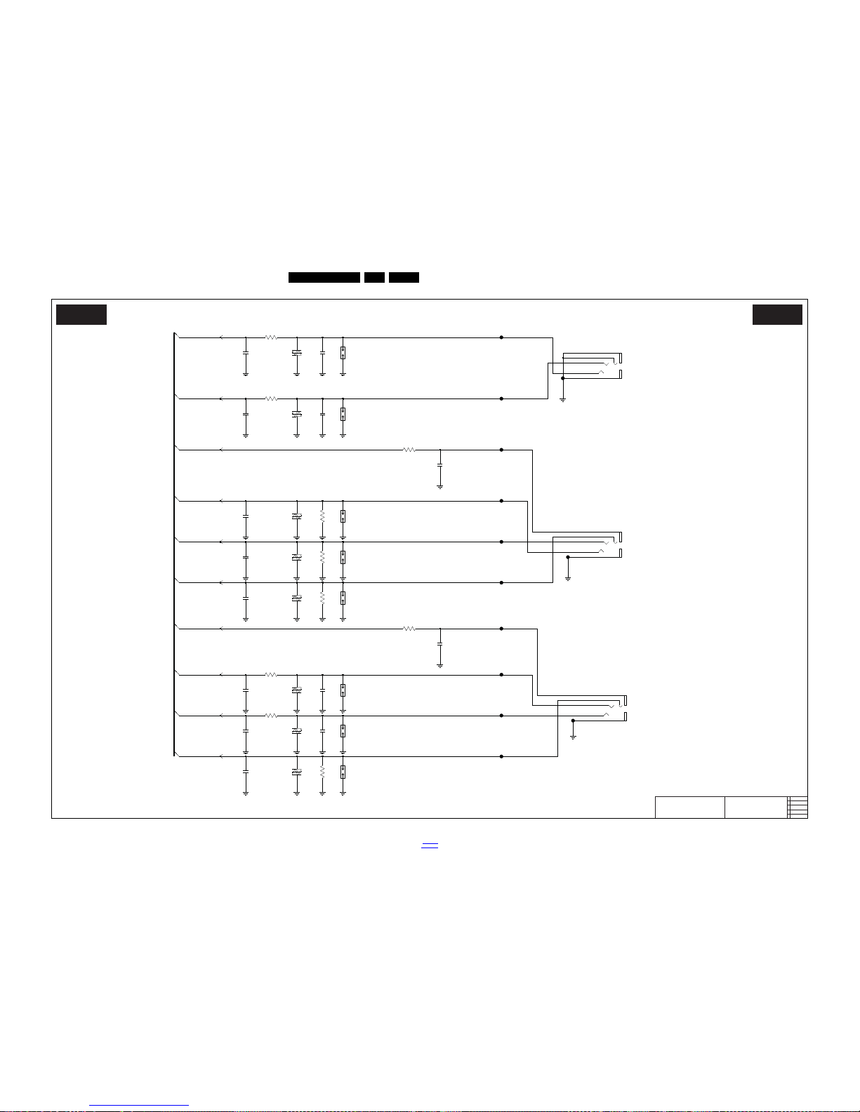
EN 90QFU1.2E LA 10.
Circuit Diagrams and PWB Layouts
2014-Jan-10
back to
div. table
10-1-32 B06F, Analogue externals
19370_158_130227.eps
130227
Analogue externals
B06F B06F
2012-11-22
4
3104 313 6612
Analogue externals
CVBS +
YPBPR
AUDIO VGA/DVI
AUDIO CVBS / YPBPR
1VC4
150R
3VC2
150R
3VC0
3VC6
1K0
FVC6
FVC1
100p
2VC4
1VC3
FVC4
1K0
3VC3
100p
2VCA
3VC4
1K0
1VC6
3VC9
47R
3VC8
47R
3VC1
150R
RES
6VC4
CDS4C12GTA
12V
FVC3
1K0
3VC7
RES
6VC0
CDS4C12GTA
12V
1VC5
MSJ-035-75C-G-RF-PBT-BRF
1VA8
1
2
3
4
5
1VC81VC2
1
2
3
4
5
MSJ-035-75C-BL-RF-PBT-BRF
1VA6
2VC3
100p
FVC5
1n0
2VCB
RES
6VC2
CDS4C12GTA
12V12V
CDS4C12GTA
6VC5
RES
2VC8
100p
FVCA
100p
2VC5
47p
2VC2
1n0
2VC7
2VC1
47p
100p
2VCD 2VCC
100p
FVC7
FVC9
2VC9
1n0
47p
2VC0
1VC7
12V
CDS4C12GTA
6VC3
RES
1VC1
FVCB
FVC2
FVCC
FVCD
RES
12V
CDS4C12GTA
6VC6
150R
3VC5
RES
FVC8
6VC7
CDS4C12GTA
12V
1n0
2VC6
12V
4
5
CDS4C12GTA
6VC1
RES
MSJ-035-75C-Y-RF-PBT-BRF
1VA4
1
2
3
VGA-RIN
PR1-IN
Y1-IN
YPBPR-RIN
YPBPR-LIN
PB1-IN
CVBS1
YPBPR-DETECTn
CVBS-DETECTn
VGA-LIN
Page 91
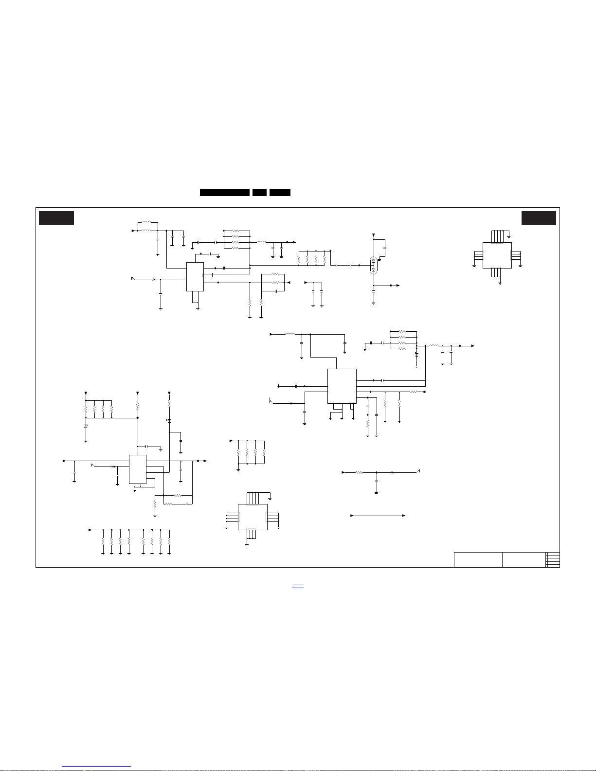
Circuit Diagrams and PWB Layouts
EN 91QFU1.2E LA 10.
2014-Jan-10
back to
div. table
10-1-33 B06G, DC-DC
19370_159_130227.eps
130227
DC-DC
B06G B06G
2012-11-22
4
3104 313 6612
DC-DC
FB
SS
EN
BOOT
VIA
VIN
SW
COMP
GNDGND_HS
ADJ
VOUT
NC
EN
VIN
HSGND
GND
VDD
PGOOD
VIA
VIA
VIA
VIA
SW
BOOTENVIN
GND
GND HS
VCC
FB
VIA
VIA
VIA
VIA
+2V5
1%
3URA
68K
10R
3UWJ-2
2UR3
FURA
100n
+3V3
FUW3
100n
2UWY
+5V
RES
11
2
5UR5
30R
1
6
75
4
9
83
10
7UR6
RT7297CHZSP
Φ
STEP DOWN
2URJ
1n0
10u
2UWT
+2V5
22u
2UR9
+3V3
45
3UWC
470K1%
RES
3UWK-4
100R
1M0
3UR4
2UR6
100n
10u
2UR5
100R
3UWK-1
1 8
3n3
2URG
RES
22u
2URC
+3V3
RES
FUW4
3UR3-4
33R
+3V3
47K
3UWL
GND-3V3r
FUW2
+12Vb
22u
+22V
2URD
100p
2URH
IUR2
+12Vb
RES
3UWA-3
4K7 RES
IUWE
+5V
CUR5
IURA
6UW2
BAV99 COL
1n0
2UR2
+2V5-F
3UWJ-3
10R
5UR6
3u6
2UR7
10u
1%
IURC
3UWF
220K
IURM
IURL
3UWJ-1
10R
1%
120K
3UR5
1n0
2UR0
DBG
+12Vb
LTST-C190CKT
6UW1
RES
470R
3UWH-1
3UR3-2
33R
IUR3
+3V3
+3V3
IUR8
10n
2URF
72
8
9
5
1
4
63
RT9025-12GSP
7UW2-1
IURB
RES
2UR8
22u
3UWH-2
470R
IURK
2UR1
100n
FUR1
33R
3UR3-3
PDZ5.1B(COL)
6UW0RES
RES
470R
3UWH-3
IUR0
RES
IURD
1n0
2UWS
RES
27
IURF
3UWK-2
100R
RES4K7
3UWA-4
2UWU
100n
470R
3UWG-4
RES
100n
2UY2
3UWM
5UR2
4u7
1R0
RES
3UWH-4
470R
1%
3URB
22K
470R
3UWG-2
3UWB
330R
DBG
RES
100n
RES
2URB
3UWA-1
4K7
IURE
2UY3
1u0
GND-3V3r
GND-3V3r
5UR3
30R
1%
3UR7
220K
IUR4
RES
33R
3URG-4
GND-3V3r
RES3URG-3
33R
2URE
100n
3UWK-3
RES
3 6
100R
+2V5
2UY8
100p
IUWF
22u
2UY7
2UY6
22u
30R
5UR1
13
141516
17
18
+12Vb
IUR9
10
19
20
21
22
232425
26
11
12
1
RT8288AZSP
7URA-2
4
5
6
8
9
2
3
7
RT8288AZSP
7URA-1
16
17
18
2UWR
1u0
21
22
232425
26
11
12
13
14
15
RT9025-12GSP
7UW2-2
10
19
20
5%
6K8
3URF
1M0
3URC
2UWV
22u
RES
33R
3URG-2
RES
3URG-1
33R
RES
GND-3V3r
3UWG-1
470R
2UR4
1n0
2UWW
1n0
33R
3UR3-1
22u
2URA
IURn
2URK
1n0 1n0
2URL
RES
22K
3UR6
RES
GND-3V3r
1%
3UWD
22K
RES4K7
3UWA-2
RES
6UW3
B230LA-M3
RES
+5V
+5V
3UWG-3
470R
10R
3UWJ-4
100n
2UY5
2UY1
100n
GND-3V3r
DETECT12V
ENABLE+3V3
ENABLE+2V5
ENABLE+2V5
Page 92
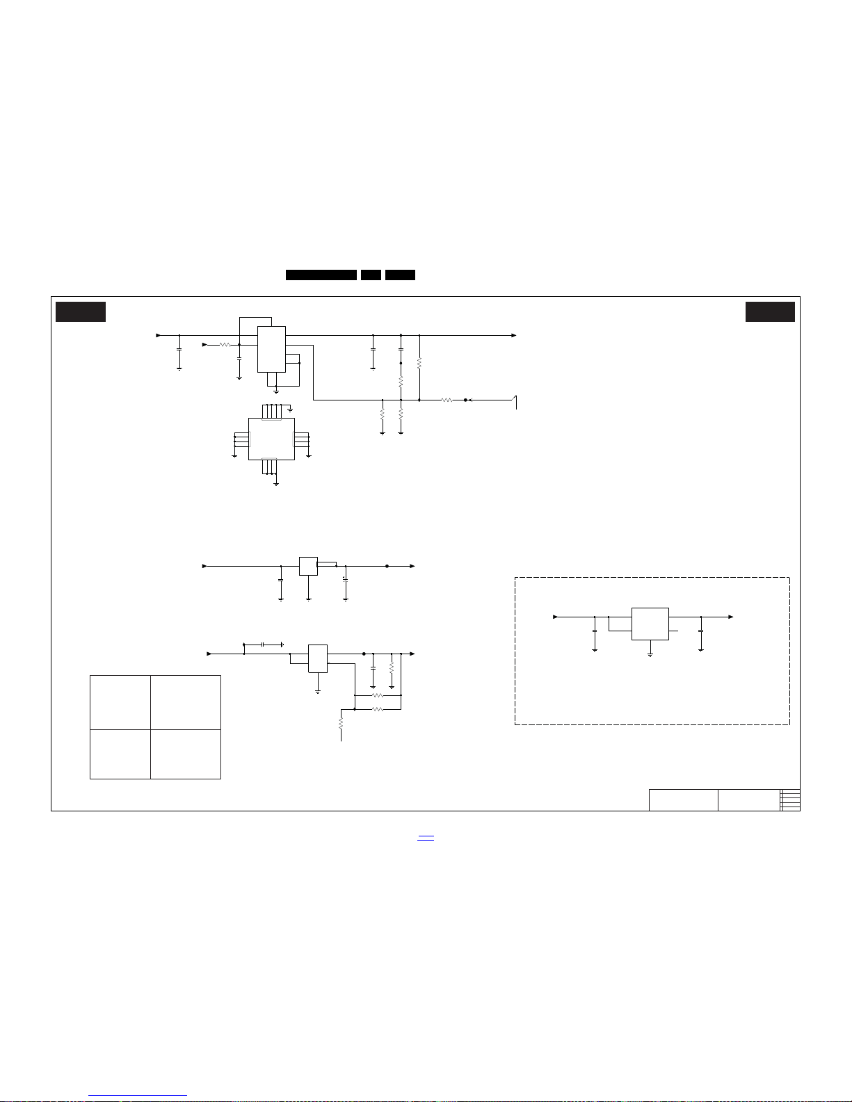
EN 92QFU1.2E LA 10.
Circuit Diagrams and PWB Layouts
2014-Jan-10
back to
div. table
10-1-34 B06H, DC-DC
19370_160_130227.eps
130227
DC-DC
B06H B06H
2012-11-22
4
3104 313 6612
DC-DC
+1V1-DVBT2 (*) 3UU5
1.10 V RES
1.20 V 680 kΩ
COM
OUTIN
VOUT
EN
GND
VIN
NC
EN ADJ
GND
OUTIN
ADJ
VOUT
NC
EN
VIN
HSGND
GND
VDD
PGOOD
VIA
VIA
VIA
VIA
Optional
7UV2
3
2
4
51
3
2
4
RT9030-11GU5
7UV0
NX1117C12Z
1
FUV1
3UU1
22K
IUV3
IUU7
+3V3
IUU2
+1V2-FA
1%82K
3UU6
43
2
15
RT9187GB
7UV1
3UU4
220K 1%
+1V1-DVBT2
IUU8
1%
120K
3UV1
2UVB
10u
2UUA
1n0
22u
2UU5
3UV6
100R
RES
+3V3
22u 16V
2UV7
10u
2UVD
3UV2
33K1%
3UV5
68K1%
FUU1
IUU3
10u
2UV9
1u0
+3V3
2UU1
100n
2UV6
10u
FUV2
2UU0
RES
3UU7
82K 1%
*
680K
3UU5
+1V1-FA
+1V5
3UU2
1R0
2UVC
10u
IUV1
+5V
25
26
11
12
13
141516
17
0181
19
20
21
222324
8
9
5
1
4
3
6
7UU1-2
RT9025-12GSP
7UU1-1
RT9025-12GSP
72
+1V1-FA
SENSE+1V1-DVBT2
Page 93
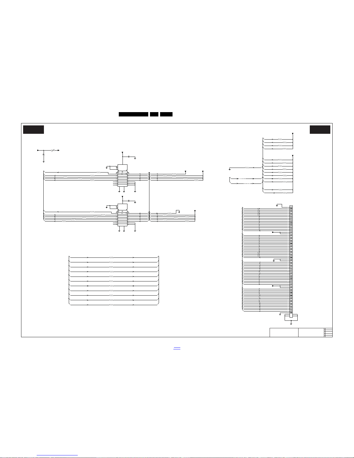
Circuit Diagrams and PWB Layouts
EN 93QFU1.2E LA 10.
2014-Jan-10
back to
div. table
10-1-35 B06I, CI conditional access
19370_161_130227.eps
130227
CI conditional access
B06I B06I
2012-11-22
4
3104 313 6612
CI conditional access
GND
VCC
GND_HS
G3
1
2
3EN2
3EN1
+T
GND
VCC
GND_HS
G3
1
2
3EN2
3EN1
2PA1
22u 16V
20
15
14
13
12
11
1
10
21
19
3
4
5
6
7
8
9
18
17
16
74LVC245ABQ
7PA2
2
3PA5
10K
3PAF
10K
10K
3PASRES
RES
+5VCA
+5VCA
3PAY
10K
RES
+3V3
9PAA
33R
3PAL
+3V3
+3V3
+5V
9PAB
RES
100n
2PA3
3PA3
100R
10K
1
8
3PAA-1
3PA1
10K
3PAA-2
2
7
0R3
3PA7
10K
4
5
RES
3PA8-4
100R
10K
3PAV
10K
RES3PAU
3PA4
100R
+3V3
3PAN
10K
6
+5VCA
3PW2-3
33R
3
+3V3
10K
3PAP
20
15
14
13
12
11
1
10
21
19
2
3
4
5
6
7
8
9
18
17
16
7PA1
74LVC245ABQ
3PA6
+3V3
10K
3PW3
33R
3
6
8
1
3PAB-3
10K
100R
3PA9-1
10K
3PAW RES
6
3PA2
100R
3PAA-3
10K
3
72
65
66
67
68
7
8
9
697071
55
56
57
58
59
6
60
61
62
63
64
46
47
48
49
5
50
51
52
53
54
36
37
38
39
4
40
41
42
43
44
45
28
29
3
30
31
32
33
34
35
18
19
2
20
21
22
23
24
25
26
27
1
10
11
12
13
14
15
16
17
1P00
92789-055LF
100K
3PAM
10K
3PAT
RES
RES3PAR
10K
100R
3PA9-3
6 3
3PW5
33R
8
3PA8-1
100R
1
27
33R
3PW2-2
6
3PA8-3
100R
3
1 8
33R
3PW1-1
3PW2-1
33R
1 8
3 6
33R
3PW1-3
27100R
3PA9-2
10K
3PAE
3PAD
10K
10K
3PAB-4
45
+3V3
33R
3PW2-4
45
54
3PA9-4
100R
5
10K3PAA-4
4
1
8
2PA2
100n
3PAB-1
10K
10K
3PAC
33R
3PW4
2
7
3PA8-2
100R
3PW1-4
45
33R
3PW1-2
33R
27
3PAB-2
2
7
CA-MIVAL
MISTRT CA-MISTRT
10K
CA-MDI1
MDI2 CA-MDI2
MDI3 CA-MDI3
MDI4 CA-MDI4
MDI5 CA-MDI5
MDI6 CA-MDI6
MDI7 CA-MDI7
MICLK CA-MICLK
MIVAL
CA-D06
CA-D07
CA-CE1n
CA-A10
CA-OEn
MDO2
CA-MDO0
CA-MDO1
CA-MDO7
MDI0 CA-MDI0
MDI1
CA-A11
CA-A09
CA-A08
CA-A13
CA-A14
CA-WEn
CA-RDY
CA-MIVAL
CA-D03
CA-MICLK
CA-A12
CA-A07
CA-A06
CA-A05
CA-A04
CA-A03
CA-A02
CA-A01
CA-A00
CA-D04
CA-D00
CA-D01
CA-D02
CA-WP
CA-D05
CA-MDI5
CA-MDI6
CA-MDI7
MOSTRT
MOVAL
CA-CD1n
CA-CD2n
CE2n
MDO2
MDO3
MDO4
MDO5
MDO6
MDO7
MDO0
MDO1
CA-INPACKn
CA-IORDn
CA-IOWRn
REGn
CA-RST
CA-VS1n
MOCLK
CA-WAITn
CA-RDY
CE2n
CA-CE1n
CA-IORDn
CA-IOWRn
CA-OEn
CA-WP
CA-INPACKn
CA-WEn
CA-RST
REGn
CE2n
CA-CE2n
REGn CA-REGn
CA-MISTRT
CA-MDI0
CA-MDI1
CA-MDI2
CA-MDI3
CA-MDI4
CA-MDO2
CA-MDO3
CA-MDO4
CA-MDO5
CA-MDO6
MOCLK
MOVAL
MOSTRT
MDO0
MDO1
MDO6
MDO5
MDO4
MDO7
MDO3
CA-CD1n
CA-CD2n
CA-VS1n
CA-WAITn
MOVAL
MOSTRT
MDO0
MDO1
MDO2
MOCLK
MDO7
MDO6
MDO5
MDO4
MDO3
CA-MOCLK
CA-MOVAL
CA-MOSTRT
Page 94
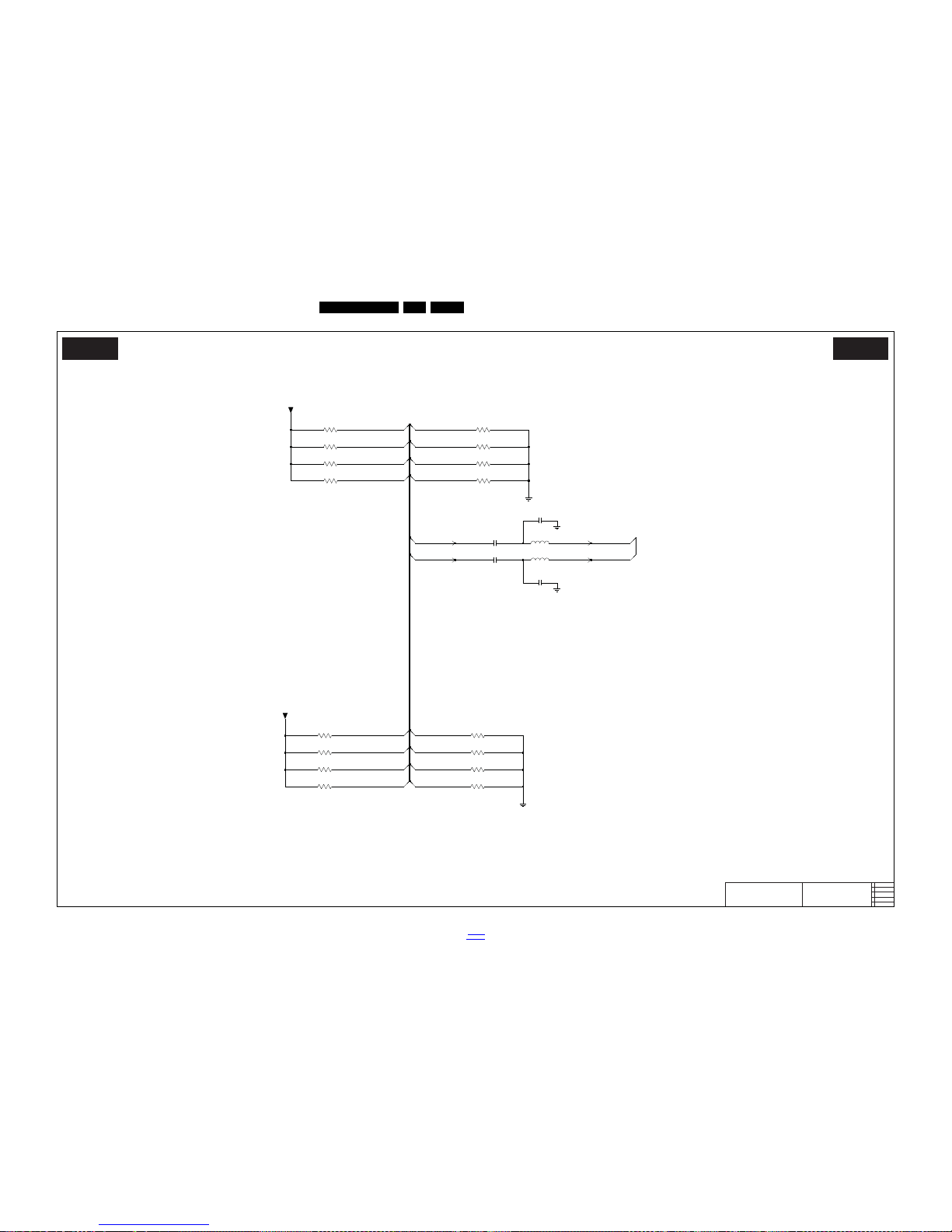
EN 94QFU1.2E LA 10.
Circuit Diagrams and PWB Layouts
2014-Jan-10
back to
div. table
10-1-36 B06J, FE
19370_162_130227.eps
130227
FE
B06J B06J
2012-11-22
4
3104 313 6612
FE
470R
3KW2
3KW7
560R
560R
3KW5
3KW3
560R
3RW2
470R
470R
3RW4
+3V3
470R
3RW8
3RW6
470R
3RW1
560R
4u7
+3V3
3KW8
470R
5FS1
10p
2FS3
RES
RES
2FS4
10p
470R
3KW6
3KW4
470R
560R
3RW3
560R
3KW1
2FS2
100n
3RW7
4u7
5FS2
560R
100n
2FS1
3RW5
560R
SOC-IF-N IF-IN-N
TS-DVBS-DATA
TS
-DVBS-CLK
TS-DVBS-VALID
TS-DVBS-SOP
TS-DVBS-DATA
TS-DVBS-CLK
TS-DVBS-VALID
TS-DVBS-SOP
TS-CHDEC-DATA
TS-CHDEC-CLK
TS-CHDEC-VALID
TS-CHDEC-SOP
TS-CHDEC-DATA
TS-CHDEC-CLK
TS-CHDEC-VALID
TS-CHDEC-SOP
SOC-IF-P IF-IN-P
Page 95
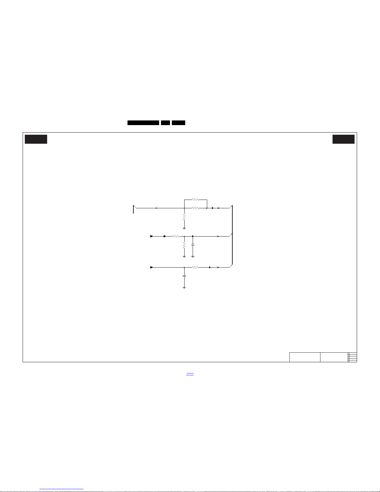
Circuit Diagrams and PWB Layouts
EN 95QFU1.2E LA 10.
2014-Jan-10
back to
div. table
10-1-37 B06K, HDMI
19370_163_130227.eps
130227
HDMI
B06K B06K
2012-11-22
4
3104 313 6612
HDMI
FHW0
IHW2
+5V
IHW1
+3V3
2HW2
100n
3HW5
12K 1%
10n
2HW1
27K
3HW4
10K
3HW3
680R
3HW2
56R
3HW1
RES
1%
RES
390R
3HW6
HDMI-ARC HEAC
IHW3
PWR5V
RREF
Page 96
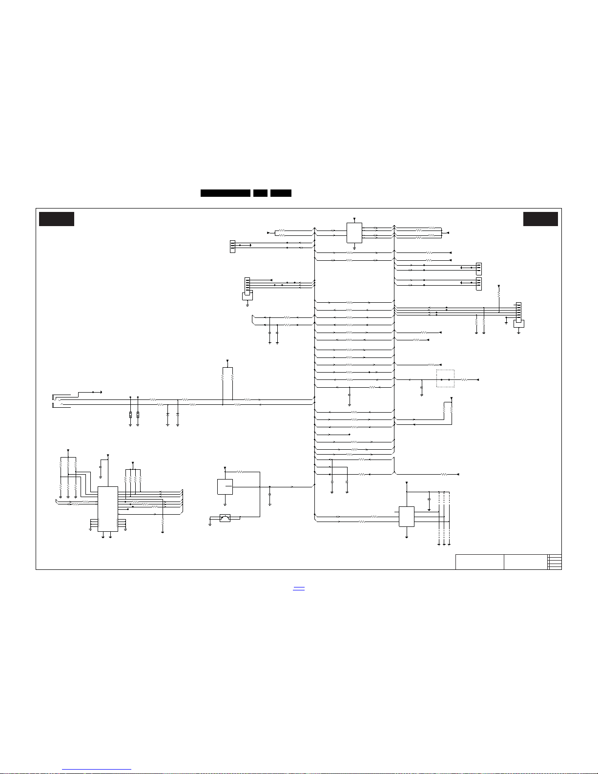
EN 96QFU1.2E LA 10.
Circuit Diagrams and PWB Layouts
2014-Jan-10
back to
div. table
10-1-38 B06L, Control, temperature sensor and service
19370_164_130227.eps
130227
Control, temperature sensor and service
B06L B06L
2012-11-22
4
3104 313 6612
Control, temperature sensor
and service
VSS
VDD
SCL
SDA
SC1
SD0
SC0
SD1
RESET
GND
VCC
VIA
A0
A1
A2
SCL
SDA
VIA
VSS GND_HS
IO0
IO1
IO2
IO3
IO4
IO5
IO6
IO7
INT
VDD
SDM
3CR0
100R
10K
3CS0
3CR3
10K
FCW5
3CWC
22K
47R
3CWJ
3CUU
10K
RES
47R
3CU7
9TW3
1
2
3
45
BM03B-SRSS-TBT
1CW4
10R
3AW0
10R
3CW5
+3V3
47R
3CWM
+3V3
3CWW
4K7
DCW5
FCW6
8 1
47R
3CS4-1
100n
2CW2
+3V3-STANDBY
1CS0
100R
3CUA
3CUW
47R
3CWT
1K0
10K
+3V3-STANDBY
3
4
5
6
78
3CS1
1CW5
BM06B-SRSS-TBT
1
2
3CUN
10K
RES
RES
3CW1
4K7
SCL
2
SDA
1
3CUK
10K
+VS
8
A0
7
A1
6
A2
5
GND
4
OS
3
7TW0
LM75BGD
3CR2100R
+3V3-STANDBY
+3V3-STANDBY
47R
3CU1
+3V3
RES
9TW5
+3V3-STANDBY
47R
3CWK
2CW3
100n
4K7
3CW0
FCWE
FCWF
+3V3
FCWV
FCS1
47R
3CUY
2CW1
100n
10K
3CUL
2TW0
100n
+3V3-STANDBY
+3V3-STANDBY
10R
3CW3
3CU6
47R
1CS1
10K
3CUP
10K
3CW2
3CU3
47R
1
2
3
4
51E06
MSJ-035-75C-B-RF-PBT-BRF
3CU5
47R
2K2
3CWV
3CRA
10K
FCWT
22K
3CWB
3CWD
+3V3
47R
3CU9
47R
9TW1
47R
RES
3CWF
3CUM
10K
RES
47R
3CU4
1CW6
BM03B-SRSS-TBT
1
2
3
45
9TW4
47R
3CWG
1CT7
SKHUBHE010
123
4
DBG
2CW5
100n
FCT9
2CT4
1n0
36
10K
3CR9
PCA9540BGD
7CW0
5
8
1
4
7
2
FCS2
1K0
3CWS
FCS0
100n
2CW4
DCW6
FCWB
DCW4
FCW4
3CU2
47R
FCWD
10K
3CWE
47R
3CS4-2
27
2AW0
1u0
+3V3
10K
3EW0
47R
3CTD
FCW1
FCWC
FCW7
10K
3CU0
100n
2CW6
2K2
3CR6
10K
3CUS
+3V3
9TW2
3CS2
47R
FCWS
FCWR
3CR7
2K2
2
3
7CT4
NCP803
1
10K
3CUT
+3V3
10K
3CUV
3CUR
10K
47R
+3V3
3CUC
+3V3
FCW2
6
FCWH
13
14
18
19
20
21
22
23
24
25
2
3
4
5
7
8
9
10
12
15
16
1
17
11
FCW0
7CW1
PCA9554BS
+3V3-STANDBY
PDZ5.1B(COL)
FCW8
3 6
6CS0
3CS4-3
47R
10K
3CR8
FCWG
47R
3CS3
DCW1
RES
9TW0
47R
3TW1
6CS1
PDZ5.1B(COL)
4K7
3CWR
3CWN
47R
4K7
3CWY
3CS4-4
47R
54
47R
3CWP
FCWU
1
2
3
45
BM03B-SRSS-TBT
1CW7
+3V3-STANDBY
4
5
67
10K
3CTY
BM05B-SRSS-TBT
1
2
3
1CWG
DCW2
3TW0
47R
3CWU
2K2
FCW3
PWRON
STANDBYn
RESET-STANDBYn
3CR1
100R
STB-RSTO
RESET-FUSION-OUTn
KYBRD
LGSEN
RESET-RF4CEn
RESET-RF4CEn
TXD-STANDBY
RXD-STANDBY
SDA-SSB
SCL-SSB
RXD-SERVICE
TXD-SERVICE
SDA-M3
EJTAG-MCU-TCK
EJTAG-MCU-TDO
EJTAG-MCU-TMS
ENABLE-WOLAN
HP-DETECT IRQ-WOLANn
AMBI-TEMP-FUS
SDMn
TEST-MOD
TEST-CON
F-OEn
ARC-SEL0
ARC-SEL1
ARC-SEL2
STB-GP6
SPLASH-ON
SCL-FE
SDA-FE
SCL-M3
STB-SCL
STB-SDA SDA-MC
STB-GP7 RESET-ETHERNETn
IRQ-EXPANDERn
SCL-SSB
SDA-SSB
CVBS-DETECTn
YPBPR-DETECTn
SC1-DETECTn
SCL-SSB
SDA-SSB
SDA-M3
SCL-M3
AMBI-TEMP
AVLINK1 DETECT12V
STB-GP3 ENABLE-WOLAN
EJTAG-MCU-TDO
EJTAG-MCU-TDI
LED
STB-GP0
STB-GP1 EJTAG-MCU-TMS
STB-TXD TXD-STANDBY
STB-RXD RXD-STANDBY
IRQ-WOLANn
DVS1
DVS2
STB-GP4
STB-GP5
KEYBOARD_IRQ-SRFn
IR RC_IRQ-RF4CEn RC_IRQ-RF4CEn
EJTAG-MCU-TDI
SCL-SRF
SDA-SRF
SCL-SSB
SCL-SRF
SCL-M3
SDA-SSB
SDA-SRF
SDA-M3
SCL-SRF
SDA-SRF
SCL-SSB
SDA-SSB
SCL-M1 SCL-FE
SDA-M1 SDA-FE
STB-GP2 EJTAG-MCU-TCK
STB-GP8
STB-GP9 LCD-PWR-ONn
STB-GP10 SDMn
Page 97
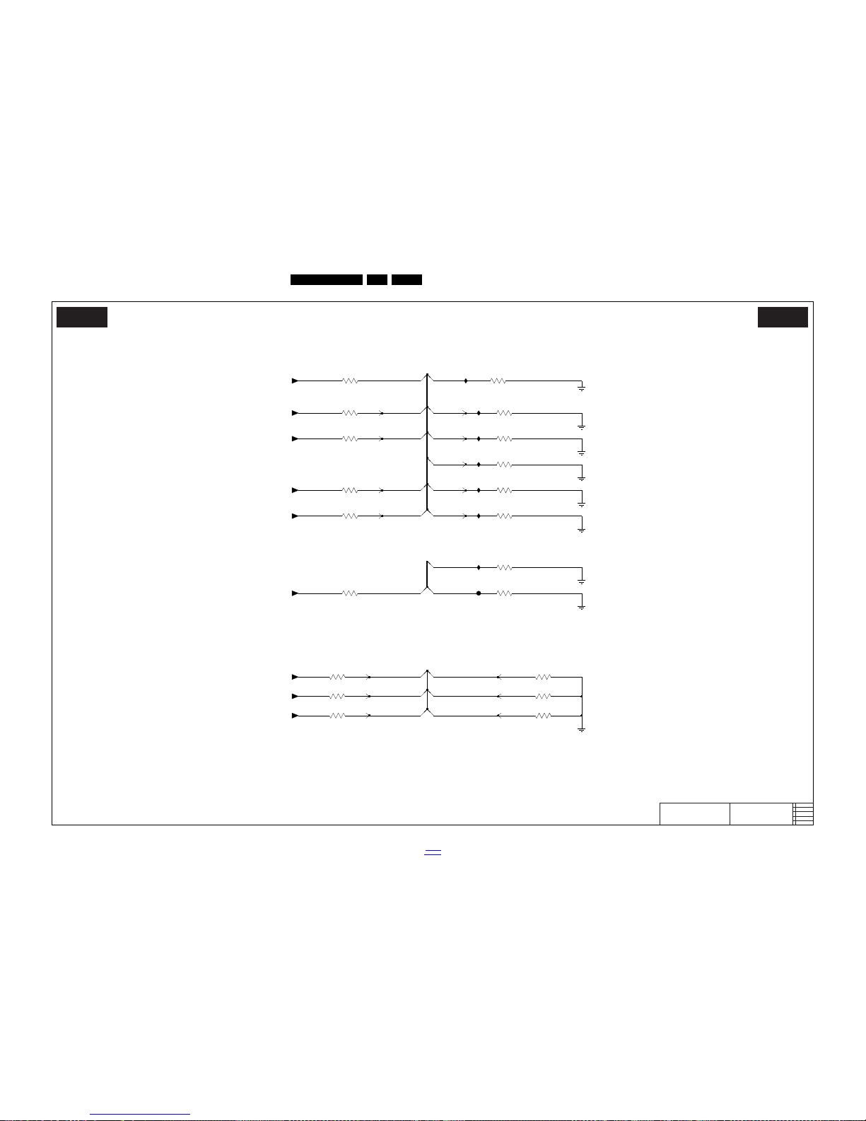
Circuit Diagrams and PWB Layouts
EN 97QFU1.2E LA 10.
2014-Jan-10
back to
div. table
10-1-39 B06M, Strap options
19370_165_130227.eps
130227
Strap options
B06M B06M
2012-11-22
4
3104 313 6612
Strap options
+3V3-STANDBY
3CUD
10K
+3V3-STANDBY
ICW1
+3V3-STANDBY
ICA6
ICA5
ICA3
ICA4
ICA2
ICA1
+3V3-STANDBY
+3V3-STANDBY
3CT8
10K
10K
3CT7
FCP6
RES
3CP5
+3V3-STANDBY
10K
RES3CL1
10K10K
3CL0
3CL5
10K
10K
3CL2
RES
10K
3CP8
10K
+3V3-STANDBY
3CL8
10K
3CP6
3CL6
3CL4
10K
RES
10K
10K
3CL3 RES
10K
3CUE
RES
3CT6
10K
10K
3CTF
3CTC
10K
RES
+3V3-STANDBY
RES
10K
3CTA
+3V3-STANDBY
3CL7
TEST-CON
TEST-MOD
ENABLE-STANDBY
SPI-ENSPI-EN
RES
10K
CA-IORDn
CA-IOWRn CA-IOWRn
TEST-CON
TEST-MOD
ENABLE-STANDBY
NAND-CLE
F-OEnF-OEn
CA-WEn
CA-OEn
CA-IORDn
CA-A14CA-A14
CA-WEn
Page 98
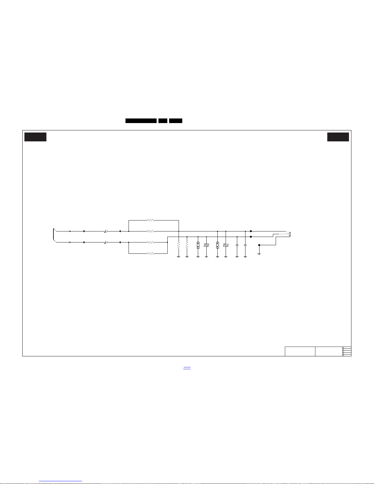
EN 98QFU1.2E LA 10.
Circuit Diagrams and PWB Layouts
2014-Jan-10
back to
div. table
10-1-40 B06N, Headphone
19370_166_130227.eps
130227
Headphone
B06N B06N
2012-11-22
4
3104 313 6612
Headphone
FDH2
2
1
3
FDH3
1DH4
MSJ-035-12D-B-AG-PBT-BRF
3DH3-2
27
12V
CDS4C12GTA
6DH1
RES
68R
2DH7
4V
4V 100u
2DH6
100u
IDHP
IDHN
2DH8
22n
68R
1 8
3DH3-1
3DH4-4
45
1DH3
1 8
1K0
3DH4-1
1K0
3 6
IDHM
68R
3DH3-3
1DH2
FDH1
6DH2
CDS4C12GTA
12V
RES
IDHL
45
22n
2DH9
HPHOR
HPHOL
68R
3DH3-4
Page 99
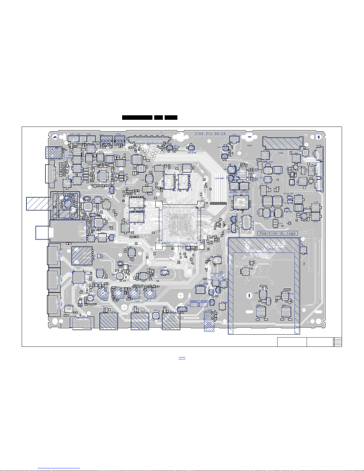
Circuit Diagrams and PWB Layouts
EN 99QFU1.2E LA 10.
2014-Jan-10
back to
div. table
10-1-41 Layout top
19370_167_130228.eps
130228
2012-11-22
4
3104 313 6612
SSB layout bottom
1C20
1C25
1C26
1C27
1C301C31
1CS0
1CS1
1CT7
1CV1 1CV2
1CV3
1CV4
1CV5
1CV6
1CW4
1CW5
1CW6
1CW7
1CWG
1CY1
1D01 1D02
1D03
1D0A
1D501D51 1D521D531D541D551D56
1DH2
1DH3
1DH4
1E00
1E01 1E02 1E03
1E06
1EF0
1F00
1FA0
1G55
1GE0
1GE1
1GE2
1GE3
1H011H021H03
1H04
1J00
1J50
1KC0
1M90
1P00
1R01
1RB0
1RD0
1T71
1UA0
1UA1
1UA2
1UP1
1VA1
1VA4
1VA6
1VA8
1VAG
1VAH
1VAJ
1VAK
1VAL
1VAM
1VAN
1VAP
1VC1
1VC2
1VC3
1VC4
1VC5
1VC6
1VC7
1VC8
2AAC
2AAD
2CAB
2CAJ
2CAK
2CAL
2CAN
2CAS
2CAT
2CAU
2CV8
2CV9
2CVA
2CVB
2CVC
2CW1
2CW6
2D0A
2D0B
2D48
2D49
2D50
2D51
2D52
2D53
2D54
2D55
2D56
2D57
2D58
2D59
2D5A
2D5B
2D5C
2D5D
2D60
2D61
2D62
2D63
2D64
2D65
2D66
2D67
2D68
2D69
2D70
2D71
2D72
2D73
2D74
2D75
2D76
2D77
2D78
2D79
2D80
2D81
2D82
2D83
2D84
2D85
2D86
2D87
2D88
2D89
2D91
2D92
2D93
2D94
2D95
2D96
2D97
2D98
2D99
2DH6
2DH7
2DH8
2DH9
2EA9
2EAA
2EAB
2EF9
2EFA
2EFB2EFC
2EFH
2EFJ
2EFK2EFL
2EFM
2EFN
2EFZ
2EHR
2EHS
2EHU
2EHV
2EHY
2EJ1
2EJ2
2EJ3
2EJ4
2EJ5
2EJ6
2EJ7
2FA0
2FA5
2FS1
2FS2
2FS3
2FS4
2FZ3
2FZ5
2FZ6
2GE1
2GE2
2GE6
2GR3
2GR4
2GR5
2GR6
2GR7
2GR8
2GR9
2GRA
2GRB
2GRC
2GRD
2GRE
2GRF
2GRG
2GRH
2GRJ
2GW2
2GW3
2GW4
2GW5
2GW6
2GW7
2GW8
2GW9
2GWA
2GWB
2GWC
2GWD
2GWE
2GWF
2GWG
2GWH
2GWJ
2GWK
2GWN
2GWR
2GWT
2GWU
2GWV
2GWW
2GWY
2HA1
2HA2
2HA4
2HA5
2HA9
2HAB
2HD6
2HDD
2J08
2J10
2J11
2J13
2J14
2J1B
2J1E
2J1G
2J1H
2J1J
2J1M
2J1N
2J1P
2J1R
2J1V
2J20
2J21
2J24
2J25
2J26
2J27
2J29
2J2D
2J2J
2J2T
2J2U
2J2V
2J2W
2J2Z
2J30
2J31
2J33
2J35
2J37
2J39
2J3D
2J3F
2J3H
2J3J
2J3K
2J41
2J42
2J59
2J7S
2J7T
2J82
2J92
2J95
2KC0
2KC1
2KC2
2KC3
2KC4
2KC5
2KC6
2KC7
2KCB
2KCC
2KCD
2KCE
2KCF
2KCG
2KCH
2KCJ
2KCK
2KCP
2KCR
2KCS
2PA1
2RB1
2RB2
2RB3
2RB4
2RB5
2RB6
2RB7
2RB8
2RB9
2RBA
2RBB
2RBC
2RBD
2RBE2RBF
2RBG
2RBH
2RBJ
2RBK
2RBL
2RBM
2RBN
2RBP
2RBR
2RBS
2RBT
2RBU
2RBV
2RBW
2RBY
2RD7
2RD8
2RD9
2RDA
2RDC
2RDD
2RDE
2RDF
2RDG
2RDJ
2RDP
2RDR
2RK02RK1
2TW0
2UA0
2UA1
2UA9
2UAA
2UAB
2UAD
2UAM
2UAT
2UAV
2UB0
2UB4
2UB6
2UB7
2UB8
2UB9
2UBA
2UBC
2UBD
2UBF
2UCA
2UCB
2UCC
2UCJ
2UCK
2UCL
2UCW
2UCY
2UF6
2UF7
2UF8
2UPC
2UPD
2UPE
2UPF
2UPG
2UPH
2UPJ
2UPK
2UPL
2UPM
2UR0
2UR1
2UR2
2UR3
2UR4
2UR5
2UR6
2UR7
2UR8
2UR9
2URA
2URB
2URC
2URD
2URE
2URF
2URG
2URH
2URJ
2UU0
2UU1
2UUA
2UV6
2UV7
2UVC
2UVD
2UWR
2UWS
2UWT
2UWU
2UWV
2UWW
2UWY
2VA8
2VAA
2VAC
2VAF
2VAG
2VAK
2VC0
2VC1
2VC2
2VC3
2VC4
2VC5
2VC6
2VC7
2VC8
2VC9
2VCA
2VCB
2VCC
2VCD
2VW1
2VW2
2VW3
2VW4
2VW5
2VW8
2VWB
2VWC
2VWD
2VWE
2VWF
2VWJ
2VWK
3AAB
3CAB
3CAF
3CAG
3CAH
3CP63CP8
3CR3
3CR6
3CR7
3CS0
3CS1
3CS2
3CS3
3CS4
3CT0
3CT1
3CT2
3CT3
3CT8
3CTA
3CTD
3CTF
3CTH
3CTJ
3CTK
3CTR
3CTU
3CTZ
3CUA
3CUD3CUE
3CUK
3CUL
3CUM
3CUN
3CUP
3CUR
3CUS
3CUT
3CUU
3CUV
3CUW
3CUY
3CV2
3CV4
3CV5
3CV8
3CV9
3CVC
3CVD
3CVE
3CVF
3CVG
3CVN
3CVR
3CVS
3CVT
3CVW
3CVY
3CW0
3CW1
3CW2
3CWE
3CWK
3CWS
3CWT
3CWW
3CWY
3CY1
3CY2
3CY3
3CY4
3CYB
3D50
3D51
3D52
3D54
3D55
3D56
3D57
3D58
3D603D61
3D62
3D63
3D70
3D71
3D72
3D73
3D74 3D75
3D76
3D77
3D78
3D79
3D82
3D83
3D90
3DH3
3EA7
3EA8
3EAC
3EAD
3EAG
3EAH
3EE2
3EF2
3EF3
3EF5
3EFH
3EFP
3EFU
3EFY
3EHR
3EHS
3EJ0
3EJ1
3EJ2
3EJ3
3EJ4
3EJ5
3EJ8
3EM8
3EM9
3EW0
3FA1
3FA2
3FA3
3FA4
3FZ0
3GD5
3GE0
3GE1
3GE7
3GE8
3GE9
3GEA
3GEG3GEH
3GEJ
3GEL
3GEM
3GEN
3GM1
3GM2
3GM3
3GM4
3GM5
3GM6
3GS5
3GW1
3GW3
3GW4
3GW5
3GW7
3GWA
3GWC
3GWD
3GWE
3GWG
3GWH
3GWN
3GWP
3HA0
3HA1
3HA2
3HA3
3HA4
3HAR
3HAV
3HAW
3HBP
3HBQ
3HDU
3HW4
3J09
3J10
3J13
3J1A
3J1B
3J1G
3J1H
3J1R
3J1W
3J1Y
3J1Z
3J20
3J21
3J24
3J25
3J2E
3J2F
3J2Q
3J2R
3J2U
3J2Z
3J36
3J37
3J3A
3J3B
3J3C
3J3D
3J3G
3J3H
3J3L
3J3M
3J3R
3J3S
3J3T
3J3U
3J3V
3J3Y
3J40
3J41
3J42
3J43
3J44
3J45
3J46
3J47
3J48
3J49
3J4E
3J4F
3J50
3J53
3J54
3J55
3JA6
3KA0
3KA1
3KC0
3KC1
3KC2
3KC3
3KC4
3KC6
3KC7
3KC8
3KC9
3KCA
3KCB
3KCE
3KW2
3KW4
3KW6
3KW8
3RB0
3RB1
3RB3
3RD0
3RD1
3RD3
3RD4
3RD5
3RD7
3RD8
3RDA
3RDB
3RW2
3RW4
3RW6
3RW8
3TW0
3TW1
3UA8
3UAB
3UAC
3UAW
3UC9
3UG9
3UR3
3UR4
3UR5
3UR6
3UR7
3URA
3URB
3URC
3URF
3UU1
3UU2
3UU4
3UU5
3UU6
3UU7
3UV6
3UWA
3UWB
3UWC
3UWD
3UWF
3UWG
3UWH
3UWK
3UWL
3UWM
3VAA
3VAD
3VAK
3VC0
3VC1
3VC2
3VC3
3VC4
3VC5
3VC6
3VC7
3VC8
3VC9
3VW3
3VW4
3VW5
3VW6
3VW7
3VW8
3VW9
3VWA
3VWD
3VWF
3VWG
3VWH
3VWJ
3VWK
3VWL
3VWM
3VWN
3VWP
3VWR
3VWS
3VWV
3VWW
5D00
5D01
5D50
5D51
5D70
5D71
5D74
5D76
5D77
5D79
5D805D83
5D85
5EF1
5EH0
5FA1
5FA4
5FA5
5FA6
5FA7
5FS1
5FS2
5HD5
5J05
5J0R
5KA0
5KA1
5KC0
5KC1
5KC55KC6
5KC7
5KC8
5KC9
5RB0
5UAA
5UB1
5UC0
5UC1
5UC2
5UP5
5UP6
5UR1
5UR2
5UR3
5UR6
6CS06CS1
6D0A
6DH16DH2
6EF2
6GE0
6GE1
6GE2
6GE3
6GS1
6RB0
6UAF
6UC0
6UC2
6UP6
6UW0
6UW1
6UW3
6VAB
6VAF
6VC0
6VC1
6VC2
6VC3
6VC4
6VC5
6VC6
6VC7
7CT3
7CW1
7D50
7D60
7D70
7D71
7EA0
7EF0
7EH4
7EHJ
7EJ0
7EM1
7GE0
7HA0
7HA1
7HD0
7J00
7J01
7J02
7J03
7J04
7KC0
7RB0
7RD0
7RDA
7TW0
7UA2
7UAC
7UB1
7UB5
7UC2
7UC3
7UC4
7UF8
7UP2
7UR6
7URA
7UU1
7UV0
7UV2
7UW2
9CAA
9CAB
9D50
9D51
9D52
9D53
9D54
9D55
9EH8
9EHE
9EM3
9GE0
9GE1
9GE2
9GE3
9GM1
9GM2
9GM5
9GM6
9GW0
9GW2
9GW3
9GW4
9HA1
9HD9
9KC0
9KC1
9RB0
9RB6
9RB7
9RB8
9RB9
9RD0
9RD1
9RD3
9TW0
9TW1
9TW2
9TW3
9TW4
9TW5
9UA1
BGV1
BGV2
BGV3
BGV4
BGV5
BGV6
BGV7
BGV8
BGV9
BGVA
BGVB
BGVC
BGVD
BGVE
BGVF
BGVG
BGVH
BGVJ
BGVK
BGVL
BGVM
BGVN
DB00
DB03
DB09
DB10
DB11
DB12
DB17
DB19
DB21
DB22
DB25
DB26
DB31
DB32
DB34
DB40
DB41
DB42
DB43
DB48
DB49
DB50
DB52
DB53
DB56
DB57
DB61
DB66
DB71
DB76
DB79
DB90
DB93
DBA2
DBA5
DCW4
DRD0
DRD1
Page 100
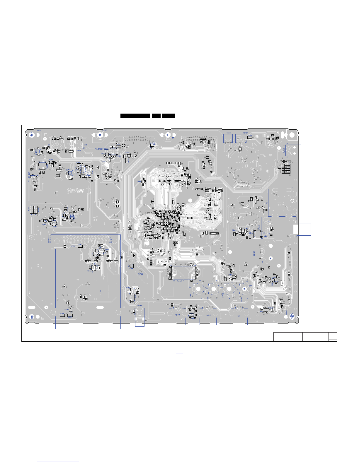
EN 100QFU1.2E LA 10.
Circuit Diagrams and PWB Layouts
2014-Jan-10
back to
div. table
10-1-42 Layout bottom
19370_168_130228.eps
130228
2012-11-22
4
3104 313 6612
SSB layout top
1EA0
1EM0
1GS1
1TA1
2AAE
2AAV
2AAW
2AW0
2CAA
2CAD
2CAM
2CAP
2CAR
2CT4
2CW2
2CW3
2CW4
2CW5
2EA0
2EA1
2EA2
2EA3
2EA4
2EA5
2EA6
2EA7
2EF0
2EF1
2EF2
2EF3
2EF5
2EF6
2EF7
2EF8
2EFF
2EFG
2EFP
2EFS
2EFT
2EFU
2EFV
2EH9
2EHJ
2EHL
2EHM
2EHN
2EHP
2EHT
2EHW
2EM0
2EM1
2EM2
2EM3
2EM4
2EM5
2EM6
2EM7
2FA1
2FA2
2FA3
2FA7
2FA8
2FA9
2FAA
2FAB
2FAC
2FAD
2FAE
2FAF
2FAG
2FAH
2FW3
2FW4
2FW5
2FW6
2FZ1
2FZ2
2FZ4
2GE0
2GE3
2GE4
2GE5
2GS1
2GS2
2GS3
2GS5
2GWL
2GWM
2GWP
2GWS
2GY1
2GY2
2GY3
2GY4
2GY5
2GY6
2GY7
2GY8
2GY9
2GYA
2HAA
2HAD
2HAF
2HAG
2HAJ
2HAK
2HAL
2HAM
2HAN
2HAP
2HB4
2HB5
2HD0
2HD1
2HD3
2HD5
2HW1
2HW2
2J00
2J01
2J02
2J03
2J04
2J05
2J06
2J07
2J09
2J12
2J15
2J16
2J17
2J18
2J19
2J1A
2J1C
2J1D
2J1F
2J1K
2J1L
2J1Q
2J1S
2J1T
2J1U
2J1W
2J1Z
2J22
2J23
2J28
2J2A
2J2B
2J2C
2J2E
2J2F
2J2G
2J2H
2J2K
2J2L
2J2M
2J2N
2J2P
2J2R
2J2S
2J2Y
2J32
2J34
2J36
2J38
2J3A
2J3B
2J3C2J3E
2J3G
2J3M
2J3N
2J3P
2J3R
2J3S
2J3T
2J3U
2J3V
2J3W
2J3Y
2J3Z
2J40
2J43
2J44
2J45
2J46
2J47
2J48
2J49
2J4A
2J4B
2J4C
2J4D
2J4E
2J4F
2J4G
2J4H
2J4J
2J4L
2J4M
2J4N
2J4P
2J4R
2J4S
2J4T
2J4U
2J4V
2J4W
2J4Y
2J4Z
2J50
2J51
2J52
2J53
2J54
2J55
2J56
2J58
2J5A
2J5B
2J5C
2J5D
2J5F
2J5G
2J5H
2J5K
2J5L
2J5M
2J5N
2J5P
2J5R
2J5S
2J5T
2J5U
2J5V
2J5W
2J5Y
2J5Z
2J60
2J61
2J62
2J63
2J64
2J65
2J66
2J67
2J68
2J69
2J6A
2J6B
2J6C
2J6D
2J6E
2J6F
2J6G
2J6H
2J6J
2J6L
2J6M
2J6N
2J6P
2J6R
2J6S
2J6T
2J6U
2J6V
2J6W
2J6Y
2J6Z
2J70
2J71
2J72
2J73
2J74
2J75
2J76
2J77
2J78
2J79
2J7A
2J7B
2J7C
2J7D
2J7E
2J7F
2J7G
2J7H
2J7J
2J7K
2J7L
2J7P
2J7R
2J7U
2J7V
2J7W
2J7Y
2J7Z
2J80
2J81
2J83
2J84
2J85
2J86
2J87
2J88
2J89
2J90
2J91
2J93
2J94
2J96
2J97
2J98
2J99
2JA0
2JA1
2JA2
2JA4
2KCL
2PA2
2PA3
2RD0
2RD1
2RD2
2RD32RD4
2RD5
2RD6
2RDB
2RDH
2RDK
2RDL
2RDM
2RDN
2RDS
2RDT
2TA1
2TA2
2TA3
2UA2
2UA3
2UA4
2UA5
2UAJ
2UAK
2UAL
2UAN
2UAP
2UAR
2UAS
2UAU
2UAW
2UB3
2UBB
2UBE
2UBG
2UBH
2UBJ
2UBK
2UC1
2UCD
2UCE
2UCF
2UCH
2UCM
2UCN
2UCP
2UCR
2UF9
2URK
2URL
2UU5
2UV9
2UVB
2UY1
2UY2
2UY3
2UY5
2UY6 2UY7
2UY8
2VA9
2VAB
2VAD
2VAE
2VAH
2VAJ
2VW6
2VW7
2VW9
2VWA
3AAA
3AAC
3AAD
3AW0
3CAA
3CAC
3CAD
3CAE
3CL0
3CL1
3CL2
3CL3
3CL4
3CL5
3CL6
3CL7
3CL8
3CP5
3CR0
3CR1
3CR2
3CR8
3CR9
3CRA
3CT6
3CT7
3CT9
3CTB
3CTC
3CTY
3CU0
3CU1
3CU2
3CU3
3CU4
3CU5
3CU6
3CU7
3CU9
3CUC
3CV3
3CV7
3CVA
3CVB
3CVM
3CVP
3CVU
3CW3
3CW5
3CWB
3CWC
3CWD
3CWF
3CWG
3CWJ
3CWM
3CWN
3CWP
3CWR
3CWU
3CWV
3CYC
3DH4
3EA1
3EA3
3EA4
3EA5
3EF4
3EFJ
3EFL
3EFM
3EFN
3EFR
3EFS3EFT
3EHJ
3EHN
3EHP
3EHT
3EHU
3EHV
3EHW
3EHY
3EJ6
3EJ7
3EM0
3EM1
3EM3
3EM4
3EM5
3EM6
3EM7
3FA7
3FA8
3FA9
3FAA
3FAB
3FAC
3FAD
3FW3
3FW4
3FW5
3FW6
3FW7
3FW8
3FZ1
3GE2
3GE3
3GE4
3GE5
3GE6
3GEB
3GEC
3GEE
3GEF
3GEK
3GM7
3GS1
3GS3
3GS4
3GS6
3GW2
3GW63GW8
3GW9
3GWB
3GWF
3GWJ
3GWK
3GWL
3GWM
3GY1
3GY5
3GY6
3GY7
3GY8
3GY9
3GYA
3GYB
3HA5
3HA6
3HAA
3HAB
3HAL
3HAP
3HAS
3HAY
3HB0
3HB1
3HB2
3HB3
3HB4
3HBS
3HD4
3HD9
3HDE
3HDS
3HDT
3HW1
3HW2
3HW3
3HW5
3HW6
3J00
3J01
3J02
3J03
3J04
3J05
3J06
3J07
3J08
3J11
3J12
3J14
3J15
3J16
3J17
3J18
3J19
3J1C
3J1D
3J1E
3J1F
3J1J
3J1K
3J1L
3J1M
3J1N
3J1P
3J1S
3J1T
3J1U
3J1V
3J22
3J23
3J26
3J27
3J28
3J29
3J2A
3J2B
3J2C
3J2D
3J2G
3J2H
3J2J
3J2K
3J2L
3J2M
3J2N
3J2P
3J2S
3J2T
3J2V
3J2W
3J30
3J31
3J32
3J33
3J34
3J35
3J38
3J39
3J3E
3J3F
3J3J
3J3K
3J3N
3J3P
3J3W
3J3Z
3J4A
3J4B
3J4C
3J4D
3J4G
3J4H
3J4J
3J4K
3J4L
3J4M
3J4N
3J4P
3J51
3J52
3JA0
3JA1
3JA2
3JA3
3JA4
3JA5
3KA2
3KA3
3KA4
3KA5
3KW1
3KW3
3KW5
3KW7
3PA1
3PA2
3PA3
3PA4
3PA5
3PA6
3PA7
3PA8
3PA9
3PAA
3PAB
3PAC
3PAD
3PAE
3PAF
3PAL
3PAM
3PAN
3PAP
3PAR
3PAS
3PAT
3PAU
3PAV
3PAW
3PAY
3PW1
3PW2
3PW3
3PW4
3PW5
3RD2
3RD6
3RD9
3RW1
3RW3
3RW5
3RW7
3TA1
3TA2
3UA4
3UA5
3UA6
3UA7
3UA9
3UAE
3UAF
3UAG
3UAH
3UAK
3UAL
3UAN3UAP
3UAR
3UAS
3UAT
3UAV
3UAY
3UB3
3UB4
3UB5
3UB6
3UB7
3UB8
3UB9
3UBA
3UBB
3UBC
3UBD
3UBE
3UBF
3UC0
3UC1
3UC2
3UC3
3UC4
3UC7
3UC8
3UCA
3UCB
3UCC
3UCD
3UCE
3UCF
3UCG
3UCN
3UCP
3UCR
3UD0 3UD1
3UG0
3UG2
3UG3
3UG4
3UG8
3UGA
3UPB
3UPD
3UPE
3URG
3UV1
3UV2
3UV5
3UWJ
3VA7
3VA8
3VA9
3VAB
3VAC
3VAE
3VAF
3VAG
3VWB
3VWC
3VWT
3VWU
5D75
5D81
5EF0
5EF4
5EF5
5EF6
5FAA
5FW3
5HA5
5HA6
5HA9
5HD0
5HD1
5HD2
5HD4
5J00
5J01
5J02
5J03
5J04
5J06
5J07
5J08
5J09
5J0A
5J0B
5J0C
5J0D
5J0E
5J0F
5J0G
5J0H
5J0J
5J0K
5J0L
5J0M
5J0N
5J0P
5KCA
5RDA
5RDB
5RDC
5RDD
5TA1
5TA2
5TA3
5UB0
5UR5
6HA1
6UAB
6UAC
6UAD
6UC1
6UP4
6UP5
6UW2
6VA8
6VA9
6VAA
6VAC
6VAD
6VAE
6VAG
6VAH
7CT4
7CW0
7EF1
7EH2
7FA1
7FAA
7FW1
7GM1
7GM2
7GS1
7GS2
7GS3
7HA2
7HA3
7HA5
7JA0
7JA2
7KA0
7PA1
7PA2
7UA0
7UA3
7UAA
7UAB
7UAD
7UAF
7UC0
7UC1
7UF7
7UF9
7UV1
80018002
9EM1
9EM2
9GA2
9GE4
9GM3
9GM4
9GS1
9GS2
9GW1
9GW5
9HA0
9HD0
9HD2
9HD4
9HD5
9HD6
9HD8
9J03
9J04
9JA3
9JA4
9JA5
9JA6
9PAA
9PAB
9RD2
9UA0
9UA2
DB01
DB02
DB04
DB05
DB07
DB08
DB13
DB14
DB15
DB16
DB18
DB20
DB23
DB24
DB27
DB29
DB30
DB33
DB35
DB36
DB38
DB39
DB44
DB45
DB46
DB47
DB51
DB54
DB55
DB58
DB59
DB62
DB63
DB64
DB65
DB67
DB68
DB69
DB70
DB72
DB73
DB74
DB75
DB77
DB78
DB80
DB81
DB82
DB83
DB85
DB86
DB87
DB88 DB89
DB91
DB92
DB94
DB95
DB96
DB97
DB98
DB99
DBA1
DBA3
DBA4
DBA6
DBA7
DBA8
DBA9
DBB0
DBB1
DBB2
DBB3
DBB4
DBB5
DBB6
DBB7
DBB8
DBB9
DBC0
DBC1
DBC2
DBC3
DBC4
DBC5
DBC6
DBC7
DC02
DC03
DC06
DC07
DCW1
DCW2
DCW5
DCW6
DEF0
DFW1
DFW2
DJA0
DJA1
DJA2
DJA3
DJA4
DJA5
DJA6
DJA7
DJA8
DJA9
DJAA
DJAB
DJAC
DJAD
DJAE
DKC0
DKC1
DVW1
DVW2
DVW3
DVW4
DVW5
DVW6
FAA0
FAA1
FAA2
FAA3
FAA4
FAA5
FAA6
FAA7
FAA8
FAA9
FAAZ
FCP6
FCS0
FCS1
FCS2
FCT2
FCT3
FCT4
FCT5
FCT6
FCT7
FCT8
FCT9
FCV1
FCV2
FCV3
FCVA
FCVB
FCVC
FCVD
FCVE
FCVF
FCVG
FCVH
FCVJ
FCVK
FCVL
FCVM
FCVN
FCW0
FCW1
FCW2
FCW3
FCW4
FCW5
FCW6
FCW7
FCW8
FCWB
FCWC
FCWD
FCWE
FCWF
FCWG
FCWH
FCWR
FCWS
FCWT
FCWU
FCWV
FCY1
FCY2
FCY3
FCY4
FCY5
FCY6
FCY7
FCY8
FCY9
FD30
FD31
FD32
FD33
FD50
FD63
FD64
FD65
FD66
FD67
FD69 FD70
FD90
FDH1
FDH2
FDH3
FEA1FEA2FEA3
FEA4
FEA5
FEA6
FEA7
FEA8
FEA9
FEAA
FEABFEAC
FEAD
FEAE
FEAH
FEF0
FEF1
FEF2
FEF3
FEF4
FEF5
FEF6
FEF7
FEF8
FEF9
FEFA
FEFB
FEFC
FEFD
FEFE
FEH1
FEH2
FEH3
FEH4
FEH5
FEH6
FEH7
FEH8
FEH9
FEJ0
FEJ1
FEJ2
FEJ3
FEJ4
FEJ5
FEJ6
FEJ7
FEJ8
FEJ9
FEJA
FEJB
FFA2
FFA3
FFA4
FFA5
FFA6
FFA7
FFA8
FFA9
FFAA
FFAB
FFAC
FFAD
FFAE
FGE0
FGE1
FGE2
FGE3
FGE4
FGE5
FGE6
FGE7
FGE8
FGR1
FGR2
FGR3
FGR4
FGR5
FGR6
FGR7
FGR8
FGR9
FGS1
FGS2
FGU0
FGU1
FGU2
FGU3
FGU4
FGU5
FGU6
FGU7
FGU9
FGUF
FGV0
FGV5
FGV6
FGV7
FGV8
FGV9
FGVA
FGVB
FGVC
FGVD
FGVE
FGVF
FGVG
FGVH
FGVJ
FGVK
FGVL
FGVM
FGVN
FGVP
FGVQ
FGVR
FGVS
FGVT
FGVU
FGVV
FGVW
FGVY
FGVZ
FGW0
FGWA
FGWB
FGWC
FGWD
FGWE
FGWF
FGWG
FGWH
FGWJ
FGWK
FGWL
FGWM
FGWN
FGWP
FGWQ
FGWR
FGWS
FGWT
FGWU
FGWV
FGWW
FGWY
FGWZ
FHA3
FHA4
FHA6
FHA7
FHA8
FHAE
FHAF
FHAG
FHAH
FHAL
FHAM
FHAN
FHAP
FHAR
FHAS
FHAV
FHAW
FHAY
FHB0
FHB1
FHB2
FHB4
FHB5
FHB6
FHB7
FHB8
FHB9
FHBA
FHBC
FHD0
FHD1
FHD2
FHD3
FHD4
FHD5
FHD6
FHD7
FHD8
FHW0
FJ01
FJ02
FJ03
FJ04
FJ05
FJ08
FJ09
FJ0A
FJ0B
FJ0F
FJ0G
FJ0H
FJ0J
FJ10
FJ16
FJA0
FKC1
FRB0
FRDA
FTA1
FTA2
FTA3
FTA4
FTA5
FTA6
FUA0
FUA1
FUA2
FUA3
FUA4
FUA5
FUA6
FUA7 FUA8FUA9
FUAAFUAB
FUAC
FUAD
FUAE
FUAF
FUAG
FUAH
FUAK
FUAL
FUAM
FUAN
FUAP
FUAT
FUAU
FUAV
FUB0
FUB1
FUB2
FUC0
FUC1
FUPA
FUR1
FURA
FUU1
FUV1
FUV2
FUW2
FUW3
FUW4
FVA1
FVA2
FVA4
FVA9
FVAA
FVAB
FVAC
FVAD
FVAE
FVAF
FVAG
FVC1
FVC2
FVC3
FVC4
FVC5
FVC6
FVC7
FVC8
FVC9
FVCA
FVCB
FVCC
FVCD
IAA0
IAA1
ICA1
ICA2
ICA3
ICA4
ICA5
ICA6
ICT1
ICT2
ICT3
ICW1
ID50
ID51
ID52
ID53
ID54
ID55
ID56
ID57
ID58
ID61
ID62
ID63
ID65
ID66
ID69
ID70
ID75
ID76
ID77
ID78
ID79
ID80
ID81
ID82
ID83
ID84
ID87
ID88
ID89
ID90
ID91
ID93
ID94
ID95
ID96
ID97
ID98
ID99
IDHL
IDHM
IDHN
IDHP
IEA1
IEA2
IEA3
IEA4
IEE0
IEE1
IEF1
IEF2
IEF3
IEH0
IEH1
IEH2
IEH3
IEH4
IEH5
IEH6
IEHJ
IEM1
IEM2
IFA3
IFA4
IFA5
IFA6
IFAA
IFW1
IFW2
IFW3
IFW4
IFW5
IGE1
IGR0
IGR1
IGR2
IGR3
IGR4
IGR5
IGR6
IGR7
IGR8
IGR9
IGRA
IGS1
IGS2
IGS4
IGS5
IGU8
IGV5
IGV7
IGW1
IGW2
IGW3
IGW4
IGW5
IGW6
IGW7
IGW8
IGW9
IHB0
IHB1
IHB2
IHB3
IHB4
IHB5
IHB6
IHD1
IHD4
IHD7
IHD8
IHDF
IHDG
IHDH
IHDK
IHDL
IHDM
IHW1
IHW2
IHW3
IJ00
IJ01
IJ02
IJ03
IJ04
IJ05
IJ06
IJ07
IJ08
IJ09
IJ0A
IJ0B
IJ0C
IJ0D
IJ0E
IJ0F
IJ0G
IJ0H
IJ0J
IJ0K
IJ0L
IJ0M
IJ0N
IJ0P
IJ0R
IJ0S
IJ10
IJ11
IJ12
IJ13
IJ14
IJA0
IJA1
IKC0
IKC1
IKC2
IKC3
IKC4
IKC5
IKC6
IKC7
IKC8
IKC9
IKCA
IKCB
IRB0
IRB1
IRD0
IRD1
IRD2
IRD3
IRD5
IRD6
IRDA
IRDB
IRDC
ITA1
IUA0
IUA1
IUA2
IUA3
IUAA
IUAB
IUAC
IUAD
IUAF
IUAJ
IUAK
IUAL
IUAM
IUAN
IUAP
IUAR
IUAS
IUAT
IUAV
IUB3
IUB4
IUB5
IUB6
IUB7
IUB8
IUB9
IUBA
IUBB
IUBC
IUC0
IUC1
IUC2
IUC3
IUC4
IUC5
IUC6
IUC7
IUC8
IUC9
IUCA
IUCB
IUCP
IUF0
IUF1
IUF3
IUF6
IUF7
IUF8
IUFP
IUFQ
IUFR
IUFS
IUFT
IUFU
IUP2
IUP4
IUPE
IUPF
IUPJ
IUR0
IUR2
IUR3
IUR4
IUR8
IUR9
IURA
IURB
IURC
IURD
IURE
IURF
IURK
IURL
IURM
IURN
IUU2
IUU3
IUU7
IUU8
IUV1
IUV3
IUWE
IUWF
IVA0
IVA1
IVW1
IVW2
IVW3
IVW4
IVW7
IVW8
 Loading...