

Philips 10H20EV8-4F, 10020EV8-4F, 10020EV8-4A Datasheet
Philips Semiconductors Programmable Logic Devices Product specification
10H20EV8/10020EV8ECL programmable array logic
113
October 22, 1993 853–1423 11164
DESCRIPTION
The 10H20EV8/10020EV8 is an ultra
high-speed universal ECL PAL
device.
Combining versatile output macrocells with a
standard AND/OR single programmable
array, this device is ideal in implementing a
user’s custom logic. The use of Philips
Semiconductors state-of-the-art bipolar oxide
isolation process enables the
10H20EV8/10020EV8 to achieve optimum
speed in any design. The SNAP design
software package from Philips
Semiconductors simplifies design entry
based upon Boolean or state equations.
The 10H20EV8/10020EV8 is a two-level logic
element comprised of 11 fixed inputs, an
input pin that can either be used as a clock or
12th input, 90 AND gates, and 8 Output Logic
Macrocells. Each Output Macrocell can be
individually configured as a dedicated input,
dedicated output with polarity control, a
bidirectional I/O, or as a registered output
that has both output polarity control and
feedback to the AND array. This gives the
part the capability of having up to 20 inputs
and eight outputs.
The 10H20EV8/10020EV8 has a variable
number of product terms that can be OR’d
per output. Four of the outputs have 12 AND
terms available and the other four have 8
terms per output. This allows the designer the
extra flexibility to implement those functions
that he couldn’t in a standard PAL device.
Asynchronous Preset and Reset product
terms are also included for system design
ease. Each output has a separate output
enable product term. Another feature added
for the system designer is a power-up Reset
on all registered outputs.
The 10H20EV8/10020EV8 also features the
ability to Preload the registers to any desired
state during testing. The Preload is not
affected by the pattern within the device, so
can be performed at any step in the testing
sequence. This permits full logical verification
even after the device has been patterned.
FEATURES
•Ultra high speed ECL device
– tPD = 4.5ns (max)
– t
IS
= 2.6ns (max)
– t
CKO
= 2.3ns (max)
– f
MAX
= 208MHz
•Universal ECL Programmable Array Logic
– 8 user programmable output macrocells
– Up to 20 inputs and 8 outputs
– Individual user programmable output
polarity
•Variable product term distribution allows
increased design capability
•Asynchronous Preset and Reset capability
•10KH and 100K options
•Power-up Reset and Preload function to
enhance state machine design and testing
•Design support provided via SNAP and
other CAD tools
•Security fuse for preventing design
duplication
•Available in 24-Pin 300mil-wide DIP and
28-Pin PLCC.
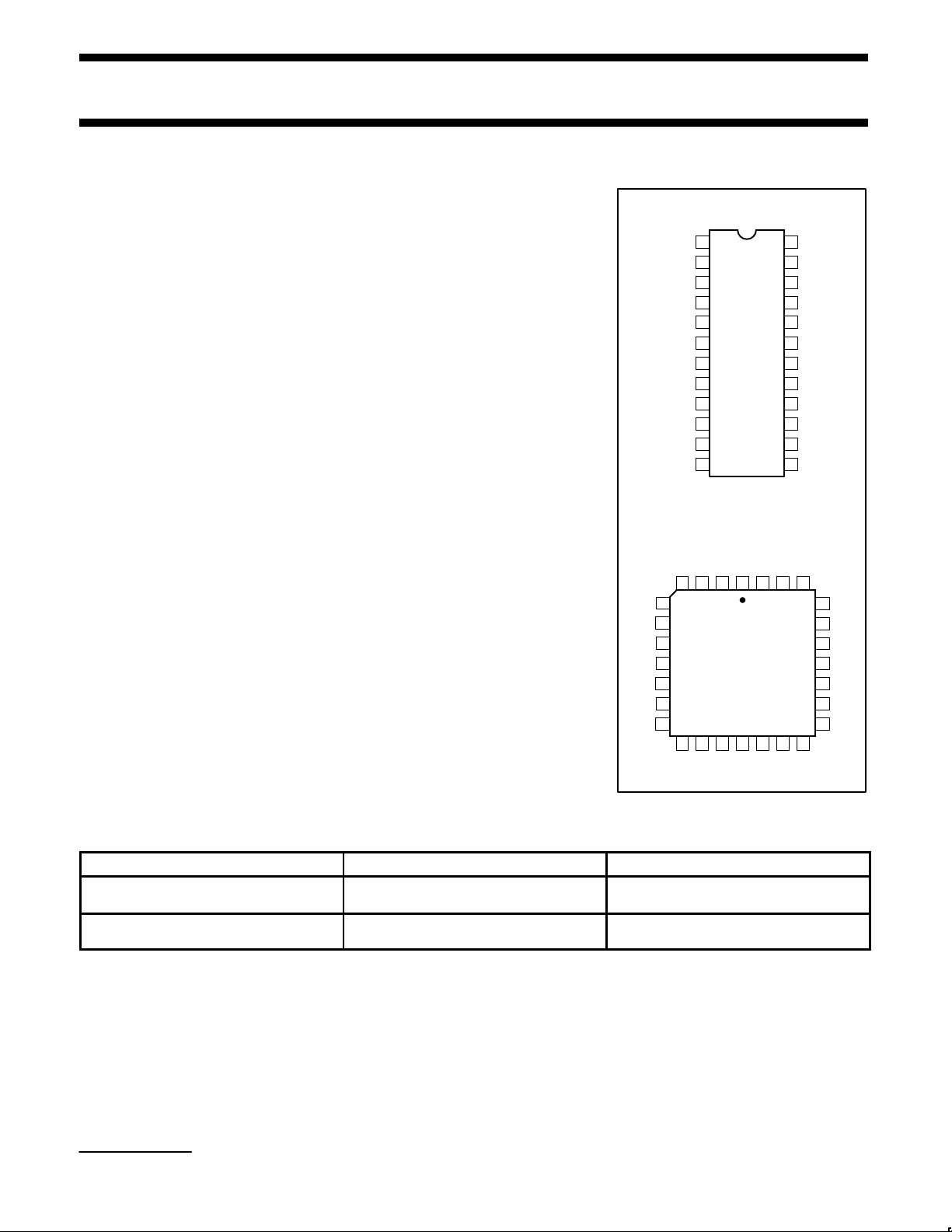
PIN CONFIGURATIONS
1
2
3
4
5
6
7
8
9
10
11
12 13
14
15
16
17
18
19
20
21
22
23
24
F Package
I
1
I
2
CLK/I
12
F
1
F
2
V
CO1
F
3
F
4
I
3
I
4
I
5
V
CC
I
11
I
10
F
8
F
7
V
CO2
F
6
F
5
I
9
I
8
I
7
I
6
V
EE
1234
5
6
7
8
9
10
11
12 13 14 15 16 17
18
19
20
21
22
23
24
25
262728
NC
NC
A Package
F
6
F
4
I1I
2
CLK/I
12
F
1
F
2
V
CO1
NC
F
3
I
3
I4I
5
I6I7I
8
I
9
F
5
F
8
F
7
V
CO2
NC
I
10
I11V
CC
V
EE
F = Ceramic DIP (300mil-wide)
A = Plastic Leaded Chip Carrier
ORDERING INFORMATION
DESCRIPTION ORDER CODE DRAWING NUMBER
24-Pin Ceramic Dual In-Line (300mil-wide)
10H20EV8–4F
10020EV8–4F
0586B
28-Pin Plastic Leaded Chip Carrier
10H20EV8–4A
10020EV8–4A
0401F
PAL is a registered trademark of Monolithic Memories, Inc., a wholly owned subsidiary of Advanced Micro Devices, Inc.
Philips Semiconductors Programmable Logic Devices Product specification
10H20EV8/10020EV8ECL programmable array logic
October 22, 1993
114
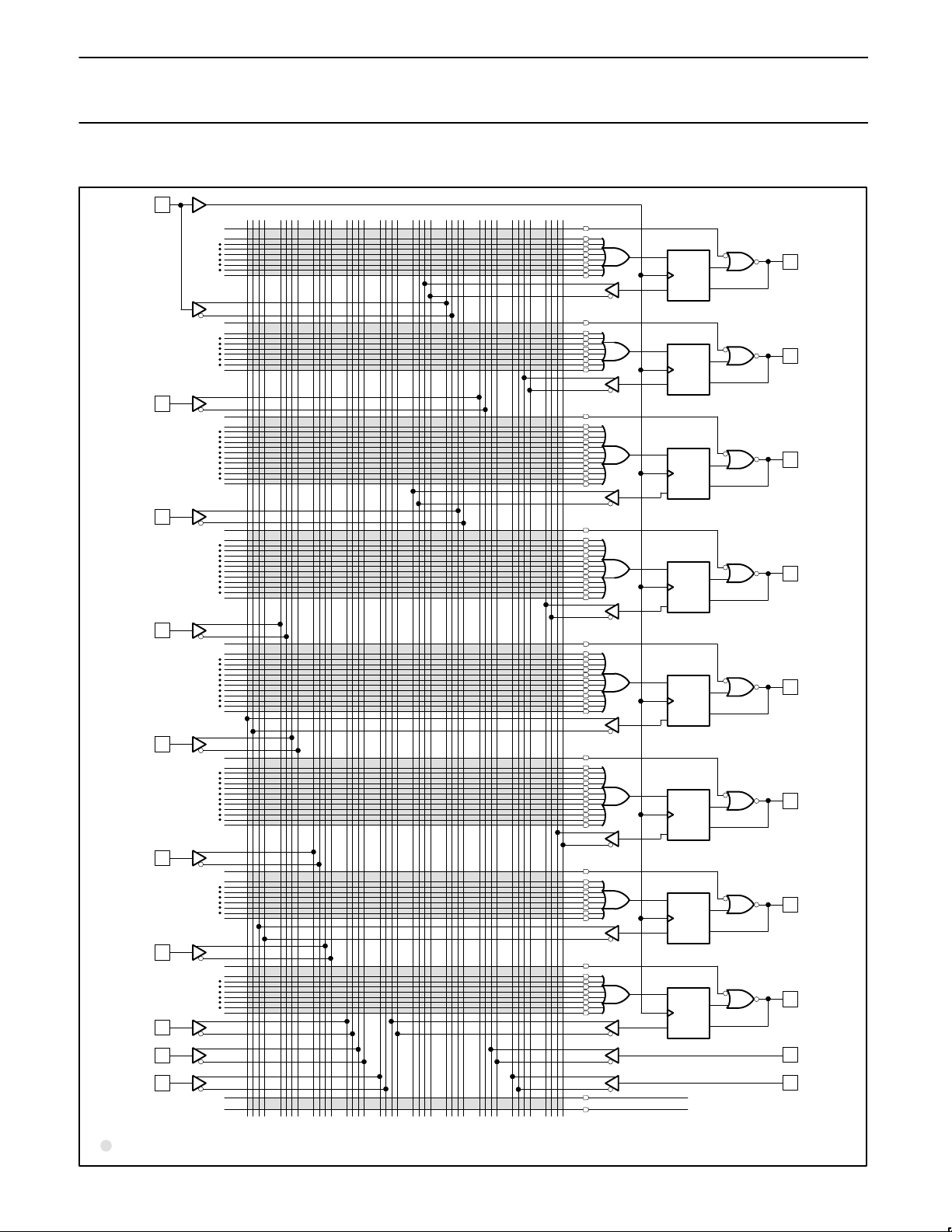
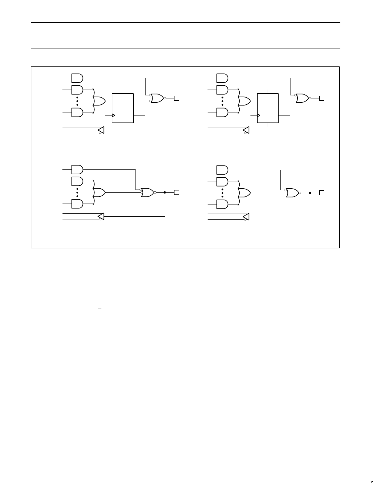
LOGIC DIAGRAM
1. All unprogrammed or virgin “AND” gate locations are pulled to logic “0”
2. Programmable connections
3. Pinout for F Package
18
OUTPUT
LOGIC
MACRO
CELL
D
OUTPUT
LOGIC
MACRO
CELL
D
OUTPUT
LOGIC
MACRO
CELL
D
OUTPUT
LOGIC
MACRO
CELL
D
OUTPUT
LOGIC
MACRO
CELL
D
OUTPUT
LOGIC
MACRO
CELL
D
OUTPUT
LOGIC
MACRO
CELL
D
OUTPUT
LOGIC
MACRO
CELL
D
ASYNCHRONOUS RESET
ASYNCHRONOUS PRESET
3
1
2
9
10
11
13
14
15
16
22
23
17
8
7
20
5
21
4
0 4 8 12 16 20 24 28 32 36
INPUT LINES
0
7
0
7
0
7
0
7
0
11
0
11
0
11
0
11
NOTES:
Figure 1. Output Logic Macrocell
F
n
V
CC
V
CC
CLK
AR
AP
D Q
Q
S
1
S
0
OUTPUT
SELECT
MUX
S
1
FEEDBACK
MUX
Philips Semiconductors Programmable Logic Devices Product specification
10H20EV8/10020EV8ECL programmable array logic
October 22, 1993
115
FUNCTIONAL DIAGRAM
OUTPUT
LOGIC
MACROCELL
OUTPUT
LOGIC
MACROCELL
OUTPUT
LOGIC
MACROCELL
OUTPUT
LOGIC
MACROCELL
OUTPUT
LOGIC
MACROCELL
OUTPUT
LOGIC
MACROCELL
OUTPUT
LOGIC
MACROCELL
OUTPUT
LOGIC
MACROCELL
PROGRAMMABLE AND ARRAY
(90 × 40)
CLK/I I
1 11
12 12 12 128888
RESET
PRESET
FFFFFFFF
FUNCTIONAL DESCRIPTION
The 10H20EV8/10020EV8 is an ultra
high-speed universal ECL PAL-type device.
Combining versatile Output Macrocells with a
standard AND/OR single programmable
array, this device is ideal in implementing a
user’s custom logic.
As can be seen in the Logic Diagram, the
device is a two-level logic element with a
programmable AND array. The 20EV8 can
have up to 20 inputs and 8 outputs. Each
output has a versatile Macrocell whereby the
output can either be configured as a
dedicated input, a dedicated combinatorial
output with polarity control, a bidirectional I/O,
or as a registered output that has both output
polarity control and feedback into the AND
array.
The device also features 90 product terms.
Two of the product terms can be used for a
global asynchronous preset and/or reset.
Eight of the product terms can be used for
individual output enable control of each
Macrocell. The other 80 product terms are
distributed among the outputs. Four of the
outputs have eight product terms, while the
other four have 12. This arrangement allows
the utmost in flexibility when implementing
user patterns.
Output Logic Macrocell
The 10H20EV8/10020EV8 incorporates an
extremely versatile Output Logic Macrocell
that allows the user complete flexibility when
configuring outputs.
As seen in Figure 1, the 10H20EV8/
10020EV8 Output Logic Macrocell consists of
an edge-triggered D-type flip-flop, an output
select MUX, and a feedback select MUX.
Fuses S
0
and S1 allow the user to select
between the various cells. S
1
controls
whether the output will be either registered
with internal feedback or combinatorial I/O.
S
0
controls the polarity of the output (ActiveHIGH or Active-LOW). This allows the user to
achieve the following configurations:
Registered Active-HIGH output, Registered
Active-LOW output, Combinatorial ActiveHIGH output, and Combinatorial Active-LOW
output. With the output enable product term,
this list can be extended by adding the
configurations of a Combinatorial I/O with
Polarity or another input.
Philips Semiconductors Programmable Logic Devices Product specification
10H20EV8/10020EV8ECL programmable array logic
October 22, 1993
116
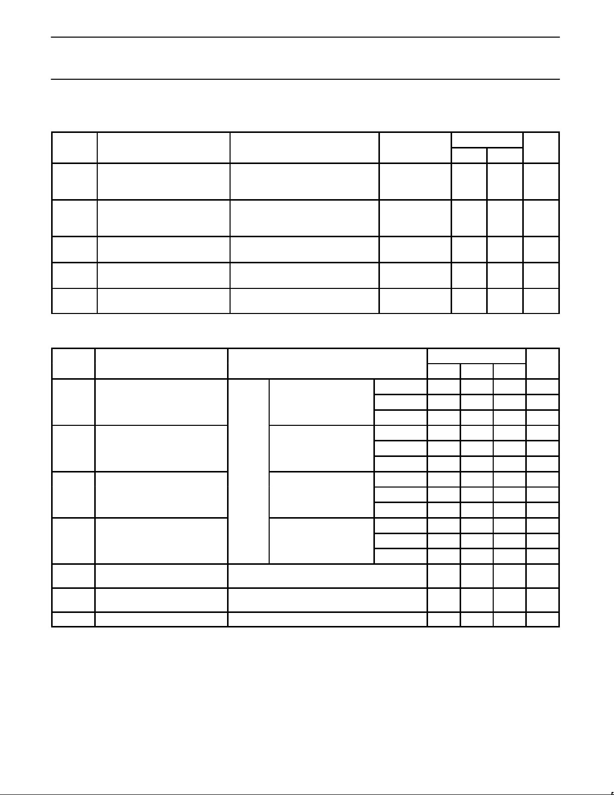
ABSOLUTE MAXIMUM RATINGS
1
SYMBOL PARAMETER RATING UNIT
V
EE
Supply voltage –8.0 V
V
IN
Input voltage (VIN should never be more negative than VEE) 0 to V
EE
V
I
O
Output source current –50 mA
T
S
Operating Temperature range –55 to +150 °C
T
J
Storage Temperature range Ceramic Package +165 °C
Plastic Package +150 °C
NOTE:
1. Stresses above those listed may cause malfunction or permanent damage to the device. This is a stress rating only. Functional operation at
these or any other condition above those indicated in the operational and programming specification of the device is not implied.
DC OPERATING CONDITIONS 10H20EV8
TEST LIMITS
SYMBOL PARAMETER CONDITIONS MIN NOM MAX UNIT
VCC, V
CO1
, V
CO2
Circuit ground 0 0 0 V
V
EE
Supply voltage (negative) –5.2 V
T
amb
= 0°C –1170 –840 mV
V
IH
High level input voltage T
amb
= +25°C –1130 –810 mV
T
amb
= +75°C –1070 –735 mV
T
amb
= 0°C –1950 –1480 mV
V
IL
Low level input voltage T
amb
= +25°C –1950 –1480 mV
T
amb
= +75°C –1980 –1450 mV
T
amb
Operating ambient temperature range 0 +25 +75 °C
NOTE:
When operating at other than the specified V
EE
voltage (–5.2V), the DC and AC Electrical Characteristics will vary slightly from specified values.
DC OPERATING CONDITIONS 10020EV8
TEST LIMITS
SYMBOL PARAMETER CONDITIONS MIN NOM MAX UNIT
VCC, V
CO1
, V
CO2
Circuit ground 0 0 0 V
V
EE
Supply voltage –4.8 –4.5 –4.2 V
V
EE
Supply voltage when opetating with the 10K
or 10KH ECL family
–5.7 V
VEE = –4.2V –1150
V
IH
High level input voltage VEE = –4.5V –1165 –880 mV
VEE = –4.8V –1165
VEE = –4.2V –1475 mV
V
IL
Low level input voltage VEE = –4.5V –1810 –1475 mV
VEE = –4.8V –1490 mV
T
amb
Operating ambient temperature range 0 +25 +85 °C
NOTE:
When operating at other than the specified VEE voltages (–4.2V, –4.5V, –4.8V), the DC and AC Electrical Characteristics will vary slightly from
their specified values.
Philips Semiconductors Programmable Logic Devices Product specification
10H20EV8/10020EV8ECL programmable array logic
October 22, 1993
117
D
AP
AR
D Q
CK Q
D
AP
AR
D Q
CK Q
Registered Active-HIGH Registered Active-LOW
D
Combinatorial Active-HIGH
Figure 2. Output Macro Cell Configurations
D
Combinatorial Active-LOW
output to
the AND array enables one to make state
machines or shift registers without having to
tie the output to one of the inputs. If a
combinatorial output is chosen, the feedback
gate is enabled from the pin and allows one
to create permanent outputs, permanent
inputs, or I/O pins through the use of the
output enable (D) product term.
OUTPUT ENABLE
Each output on the 10H20EV8/10020EV8
has its own individual product term for output
enable. The use of the D product term
(direction control) allows the user three
possible configurations of the outputs. They
are: always enabled, always disabled, and
controlled by a programmed pattern. A HIGH
on the D term enables the output, while a
LOW performs the disable function. Output
enable control can be achieved by
programming a pattern on the D term.
The output enable control can also be used
to expand a designer’s possibilities once a
combinatorial output has been chosen. If the
D term is always HIGH, the pin becomes a
permanent Active-HIGH/LOW output. If the
D term is always LOW (all fuses left intact),
the pin now becomes an extra input.
PRESET AND RESET
The 10H20EV8/10020EV8 also includes a
separate product term for asynchronous
Preset and asynchronous Reset. These lines
are common for all registers and are asserted
when the specific product term goes HIGH.
Being asynchronous, they are independent of
the clock. It should be noted that the actual
state of the output is dependent on how the
polarity of the particular output has been
chosen. If the outputs are a mix of
Active-HIGH and Active-LOW, a Preset
signal will force the Active-HIGH outputs
HIGH while the Active-LOW outputs would go
LOW, even though the Q output of all
flip-flops would go HIGH. A Reset signal
would force the opposite conditions.
PRELOAD
To simplify testing, the 10H20EV8/10020EV8
has also included PRELOAD circuitry. This
allows a user to load any particular data
desired into the registers regardless of the
programmed pattern. This means that the
PRELOAD can be done on a blank part and
after that same part has been programmed to
facilitate any post-fuse testing desired.
It can also be used by a designer to help
debug a circuit. This could be important if a
state machine was implemented in the
10H20EV8/ 10020EV8. The PRELOAD
would allow the entry of any state in the
sequence desired and start clocking from that
particular point. Any or all transitions could be
verified.
OUTPUT MACRO CELL
CONFIGURATION
Shown in Figure 2 are the four possible
configurations of the output macrocell using
fuses S
either be registered Active-HIGH/LOW with
feedback or combinatorial Active-HIGH/LOW
with feedback. If the registered mode is
chosen, the feedback from the Q
and S1. As seen, the output can
0
Philips Semiconductors Programmable Logic Devices Product specification
10H20EV8/10020EV8ECL programmable array logic
October 22, 1993
118
DC ELECTRICAL CHARACTERISTICS 10H20EV8
0°C ≤ T
amb
≤ +75°C, VEE = –5.2V ± 5%, VCC = V
CO1
= V
CO2
= GND
LIMITS
4
SYMBOL PARAMETER
1
TEST CONDITIONS
2
T
amb
MIN MAX UNITS
V
OH
High level output voltage VIN = VIH MIN or VIL MAX 0°C –1020 –840
+25°C –980 –810 mV
+75°C –920 –735
V
OL
Low level output voltage VIN = VIH MIN or VIL MAX 0°C –1950 –1630
+25°C –1950 –1630 mV
+75°C –1950 –1600
I
IH
High level input current VIN = VIH MAX 0°C
+75°C 220 µA
I
IL
Low level input current VIN = VIL MIN 0°C
Except I/O Pins +75°C 0.3 µA
–I
EE
Supply current VEE = MAX 0°C to +75°C
250 mA
DC ELECTRICAL CHARACTERISTICS 10020EV8
0°C ≤ T
amb
≤ +85°C, –4.8V ≤ VEE ≤ –4.2V, VCC = V
CO1
= V
CO2
= GND
LIMITS
4
SYMBOL PARAMETER
1
TEST CONDITIONS
2
MIN TYP MAX UNITS
VEE = –4.2V –1020 –870 mV
V
OH
High level output voltage VIN = VIH MAX or VIL MIN VEE = –4.5V –1025 –955 –880 mV
VEE = –4.8V –1035 –880 mV
Outputs Apply V
IHMIN
or V
ILMAX
to VEE = –4.2V –1030 mV
V
OHT
High level output threshold voltage Loaded one input at a time, other VEE = –4.5V –1035 mV
with 50Ω inuts at V
IHMAX
or V
ILMIN.VEE
= –4.8V –1045 mV
to –2.0V Apply V
IHMIN
or V
ILMAX
to VEE = –4.2V –1595 mV
V
OLT
Low level output threshold voltage ± 0.010V one input at a time, other VEE = –4.5V –1610 mV
inuts at V
IHMAX
or V
ILMIN.VEE
= –4.8V –1610 mV
VEE = –4.2V –1810 –1605 mV
V
OL
Low level output voltage Inuts at V
IHMAX
or V
ILMIN.VEE
= –4.5V –1810 –1705 –1620 mV
VEE = –4.8V –1830 –1620 mV
I
IH
High level input current One input under test at V
IHMAX
. Other inputs at
V
ILMIN
.
220 µA
I
IL
Low level input current One input under test at V
ILMIN
. Other inputs at
V
IHMAX
.
0.5 µA
–I
EE
VEE supply current All inputs at V
IHMAX
. 230 mA
NOTES:
1. All voltage measurements are referenced to the ground terminal.
2. Each ECL 10KH/100K series device has been designed to meet the DC specification after thermal equilibrium has been established.
Thermal equilibrium is established by applying power for at least 2 minutes, while maintaining transverse airflow of 2.5 meters/sec (500
linear feet/min.) over the device, mounted either in a test socket or on a printed circuit board. Test voltage values are given in the DC
operating conditions table. Conditions for testing shown in the tables are not necessarily worst case. For worst case testing guidelines, refer
to DC Testing, Chapter 1, Section 3, of the
Philips Semiconductors 10/100K ECL Data Handbook
.
3. Terminals not specifically referenced can be left electrically open. Open inputs assume a logic LOW state. Any unused pins can be
terminated to –2V. If tied to V
EE
, it must be through a resistor > 10K. It is recommended that pins that have been programmed as RESET,
PRESET, or CLOCK inputs not be left open due to the possibility of false triggering from internally and externally generated switching
transients.
4. The specified limits represent the worst case values for the parameter. Since these worst case values normally occur at the supply voltage
and temperature extremes, additional noise immunity can be achieved by decreasing the allowable operating condition ranges.
All inputs = VIH MAX
 Loading...