

Page 1
PlIOTOFACT*
Folder
PHILCO
MODELS
5O-T14O4,
50-T1432
5O-T14O3
5O-T14O6
(Code
124)
(Codes
(Code
125)
123,124,125),
Ul
p
*
n
O
o
O*
V
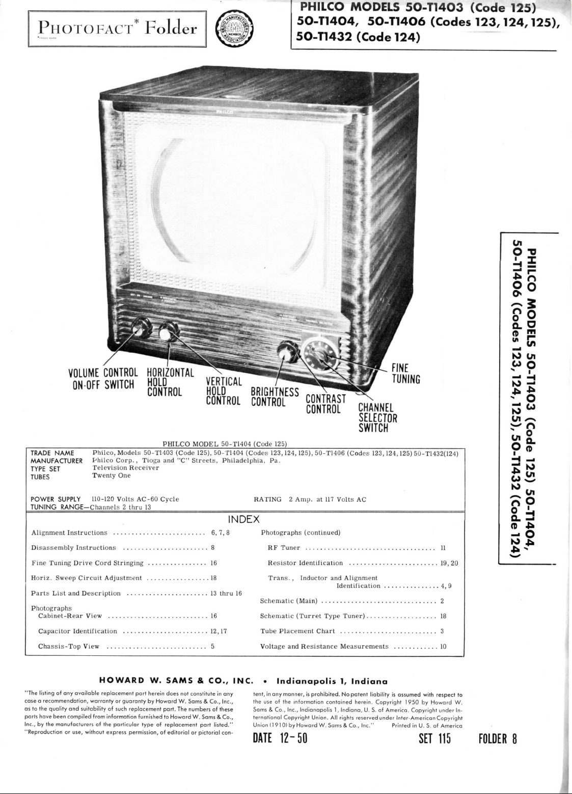
VOLUME CONTROL HORIZONTAL
(IN
(IFF
TRADE
NAME
MANUFACTURER
TYPE
TUBES
POWER
TUNING
Alignment Instructions
Disassembly
Fine Tuning Drive
Horiz. Sweep
Parts
Photographs
Cabinet-Rear View
Capacitor Identification
Chassis-Top
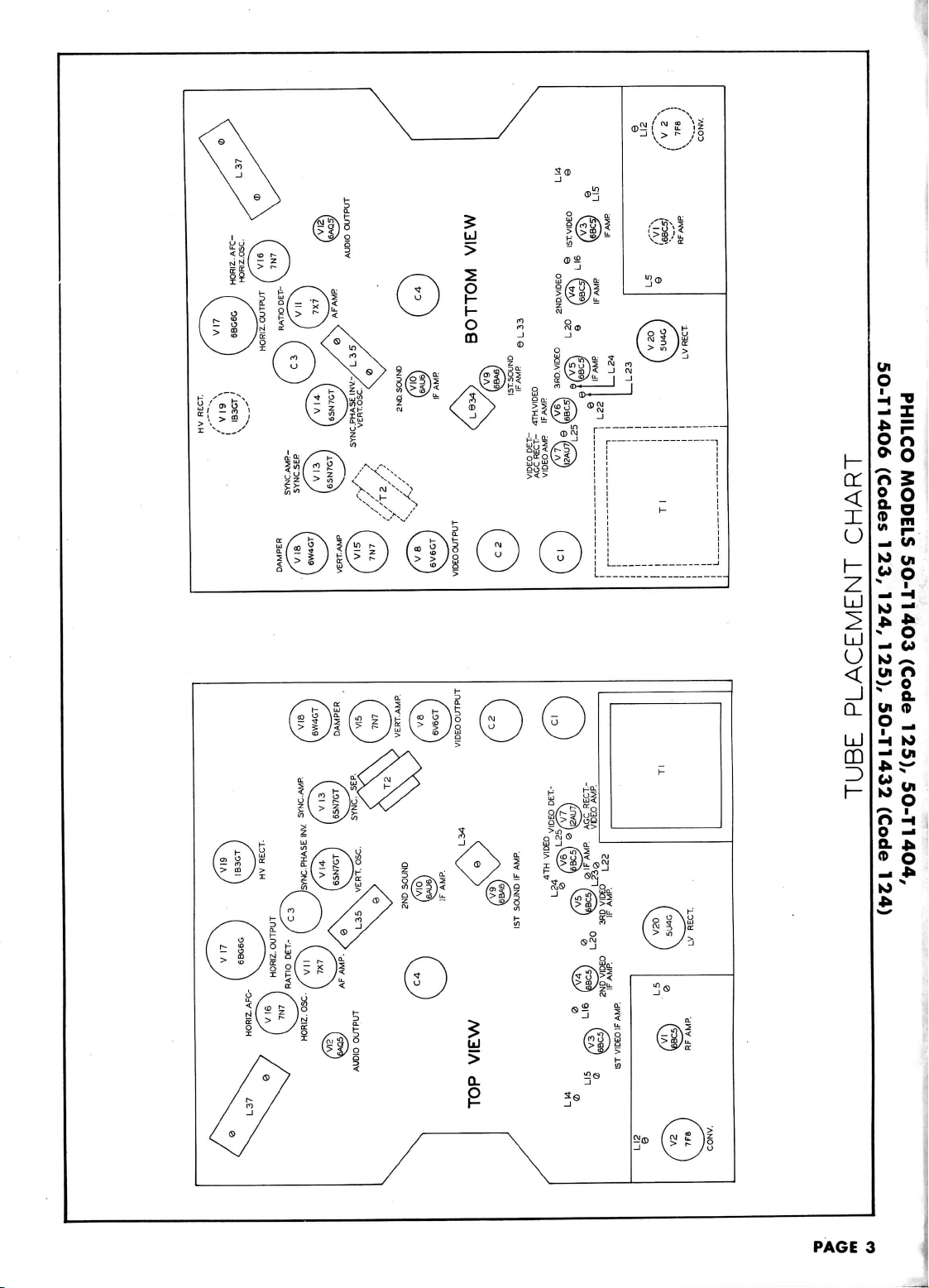
Philco, Models 50-T1403 (Code 125),
SET
Twenty
List
Philco
Television
SUPPLY
110-120
RANGE-Channels 2 thru
Instructions
Cord
Circuit
and
Description
View
SWITCH HOLD VERTICAL
CONTROL HOLD
BRIGHTNESS
CONTROL CONTROL
PHILCO
MODEL 50-T1404 (Code
Corp.,
Tioga
and
Receiver
One
Volts
AC-60
13
6, 7, 8
8
Stringing
Adjustment
5
16
18
13
12,17
"C"
Cycle
Streets,
50-T1404
Philadelphia,
INDEX
thru
16
16
ffiSSF
125)
(Codes
123,124,125),
Pa.
RATING 2 Amp.
Photographs (continued)
RF
Tuner
Resistor
Identification
Trans.,
Inductor
Schematic (Main)
Schematic
Tube
Voltage
(Turret
Placement
and
FINE
TUNING
pnMT-D..,
bUNIKUL
SELECTOR
SWITCH
50-T1406 (Codes
at 117
Volts
11
and
Identification
2
Type
Chart
3
Resistance
Measurements
123,124,125)
AC
19, 20
Alignment
Tuner)
4,9
18
50-T1432(124)
10
?§
0.0
SK
io
ui
Ul
8.2
ffl *>
HOWARD
"The listing
of any
available
case a recommendation, warranty
as
to the
quality
parts have been
Inc.,
by the
"Reproduction
and
compiled
manufacturers
or
replacement
suitability
from information furnished
of the
use, without express permission,
part
or
guaranty
of
such
replacement
particular type
W.
SAMS & CO., INC. . Indianapolis
herein does
by
not
Howard
W.
part.
The
to
Howard
of
replacement part
of
editorial
constitute
Sams & Co.,
numbers
of
W.
Sams & Co.,
listed."
or
pictorial
in any
Inc.,
these
con-
tent,
in any
manner,
the
use of the
Sams & Co., Inc., Indianapolis
ternational
Copyright Union.
Union
(1910)
by
DATE
12-50
1,
Indiana
is
prohibited.
No
patent
liability
information contained herein. Copyright
Howard
1,
Indiana,
All
rights reservedunder Inter-American Copyright
W.Sams & Co.,
is
U.
S. of
America. Copyright under
Inc."
Printed
assumed
1950
in U. S. of
with
by
SET
respect
Howard
America
115
to
W.
In-
FOLDER
Page 2
HH
[X
J
/:
J
/;
J
2
J
/
J
//f
J
/
J
/
J
/
®r~r
L-?T@|-']
®|7F«e
B
J
J
/
^
J
'/,
®!7Fe'
\T STANDARD
©Howard
CHANNEL
NOTATION
W.
Sams & Co.,
SW,
SHOWN
SCHEMATIC
Inc. 1950
IN
CHANNEL 2 POSITION
11
mi
11111
in
111
nil////////////
////////T/
THE
COOPERATION
RECEIVER
MAKES
IT
POSSIBLE
OF THE
or
MANUFACTURER
TO
BRING
MODELS.
USED
YOU
THIS
POINTS
OF
WHEN
MARKED X AT
THIS
SERVICE
DOTTED
II
PAGE
2
Page 3
®17F«
TURER
OF
'OU
THIS
TED IN
RWTTS
ARE
3EL3.
WHEN
DOTTED
D
POINTS MARKED
THIS
SERVICE
NOT
USED
IN
PARTS
X ARE
IN
ALL
ARE
BROKEN,
Page 4
PHILCO MODELS 5O-T14O3 (Code
SO-T14O6 (Codes
123,124,125),
125)
5O-T14O4,
5O-T1432 (Code
124)
Page 5
e
SI
OZA
OW1S
124)
AH
X
/^
\6IA/
•103M
(J.OE9IJ
(Code
5O-T14O4,
iani
125),
5O-T1432
(Code
124, 125),
5O-T14O3
123,
PHILCO MODELS
5O-T14O6 (Codes
Page 6
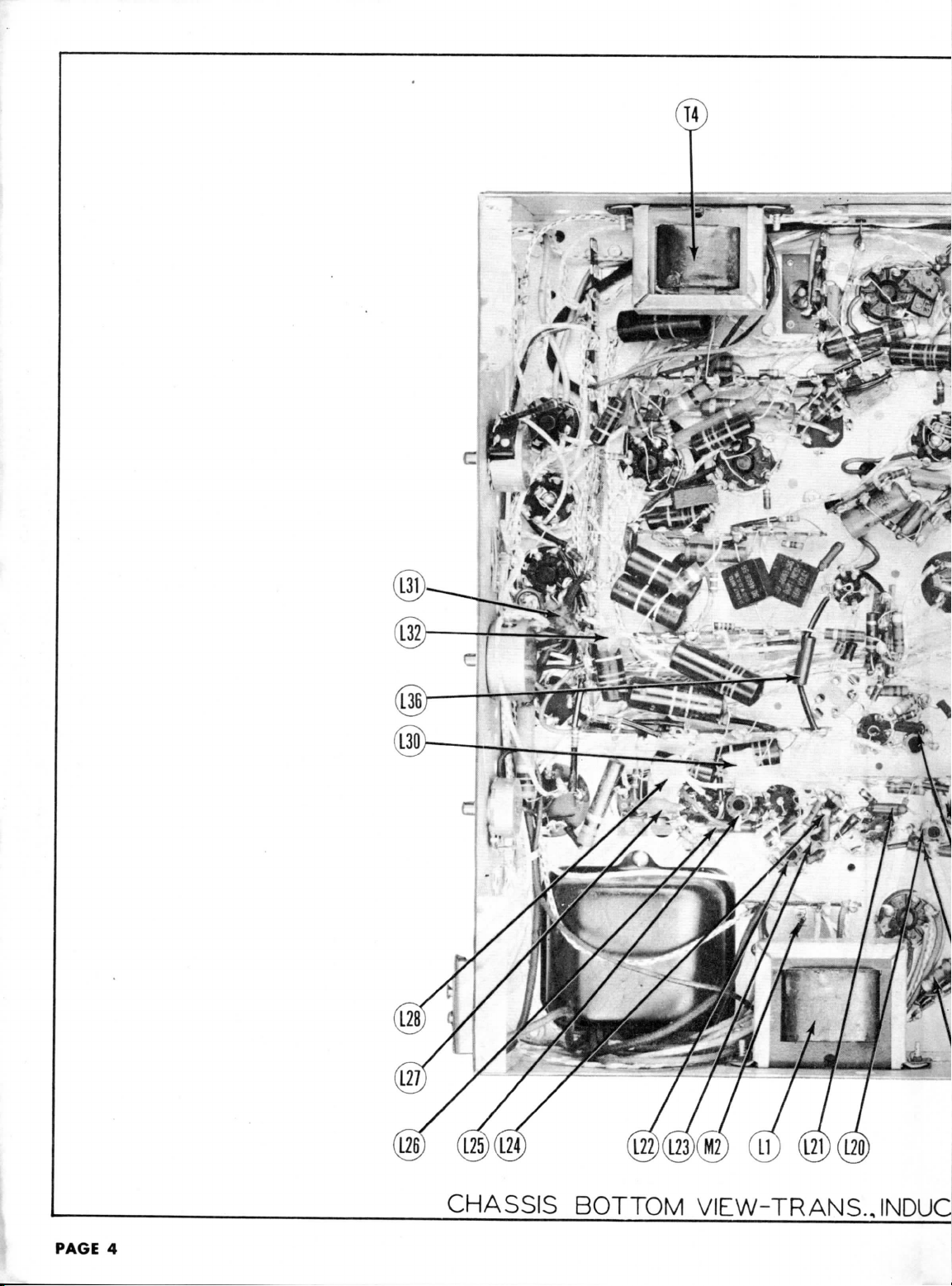
PAGE
4
CHASSIS
BOTTOM
VIEW-TRANS.JNDUC
Page 7
Ul
o
is
n 2
o
n
»
s
in
P
_.
V)
-i
O
KJ
*-^
ui
n
ui
n
O
_
•HI
IO
""
-2
^w
^
'
O
-I
o
->
a.
4a
o
3UCTOR
AND
ALIGNMENT
IDENTIFICATION
PAGE
KJ
9
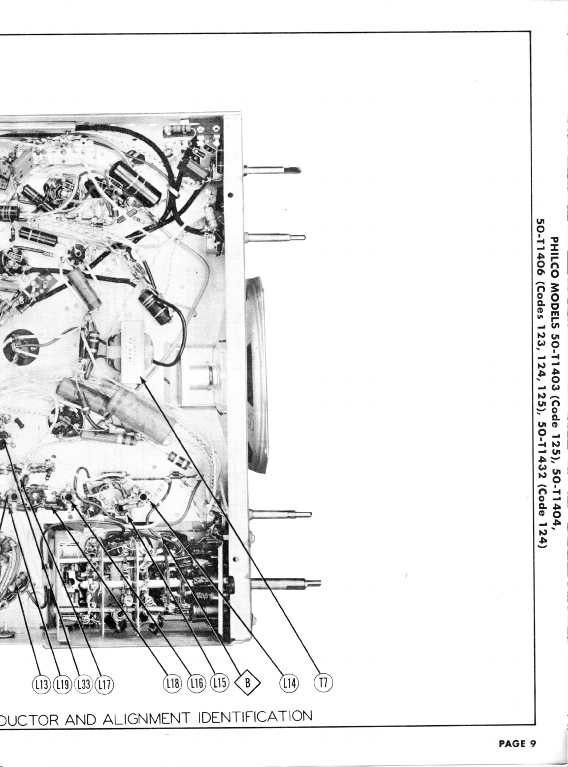
Page 8

5O-T14O4,
125),
(Code
5O-T1403
MODELS
PHILCO
124)
(Code
5O-T1432
125),
SISSVHO
124,
dOl
AOA
(Codes 123,
5O-T14O6
Page 9

If
receiver
is
In
the
codes
In
code
124
Before
attempting alignment
All and A12
A3 and
A7
and A8
Turn
the
contrast control
Connect
the
DUMMY
ANTENNA
.
001MFD
.
001MFD
.
001MFD
.001MFD
.
001MFD
Direct
Direct
Direct
Connect
the
DUMMY
ANTENNA
Direct
Connect
two
as
shown
on the
DUMMY
ANTENNA
Direct
Direct
DUMMY
ANTENNA
Direct
Direct
to
be
aligned
123 and 125
models,
AID
negative
High
of
to
High
of
to
High
of
to
High
of
to
High
tube
converter tube (V2).
Low
synchronized sweep voltage
High
tube
converter tube
Low
High
tube
converter tube (V2).
Low
High
tube
converter tube (V2).
Low
models,disconnect
remove
fully
clockwise
fully
counter-clockwise
until
the top of the
terminal
SIGNAL
GENERATOR
COUPLING
side
to pin 1
6BC5 (V6).
chassis.
side
to pin 1
6BC5
(V5).
chassis.
side
to pin 1
6BC5 (V4).
chassis.
side
to pin 1
6BC5
(V3).
chassis.
side
to
ungrounded
shield
floating
side
to
chassis.
SWEEP
GENERATOR
COUPLING
side
to
ungrounded
shield
floating
side
to
chassis.
matched
lOOKfi
schematic.
SIGNAL
GENERATOR
COUPLING
side
to
ungrounded
shield floating over
side
to
chassis.
SWEEP
GENERATOR
COUPLING
side
to
ungrounded
shield floating over
side
to
chassis.
ALIGNMENT
with
picture tube removed,
the
converter tube (V2) from
pre-set
the
adjusting
fully
counter-clockwise.
of a 1 1/2
(Grid)
Low
side
(Grid)
Low
side
(Grid)
Low
side
(Grid)
Low
side
over
over
(V2).
(i
1%)
S
OUND
ALIGNMENT
the
yellow wire
following
screws
volt
battery
SIGNAL
GENERATOR
FREQUENCY
25.
SMC
(Unmod.)
25MC
24.
SMC
26. 6MC
23.25MC
28. IMC
22.
IMC
25.
BMC
from
the
SWEEP
GENERATOR
FREQUENCY
25MC
(10MC
SWP)
SOUND
resistors
SIGNAL
GENERATOR
FREQUENCY
22.
IMC
(Unmod.
IF
ALIGNMENT
SWEEP
GENERATOR
FREQUENCY
22.
IMC
(450KC
SWP)
INSTRUCTIONS—
adjustments:
are
to pin 2 of
CHANNEL
Any
"
3
OVERALL
signal generator
GENERATOR
FREQUENCY
23MC
23.
25.
26.6MC
IF
ALIGNMENT
in
series
CHANNEL
3
)
MARKER
GENERATOR
FREQUENCY
22.
the
high
voltage lead should
VIDEO
from
the
its
socket
approximately
align
DC
align
mon
11
"
VIDEO
MARKER
SMC
SMC
USING
from
pin 2 of
DC
FM
mon
DC
to
jack. Common
Point<£>.
USING
IMC
READ
INSTRUCTIONS
CAREFULLY
IF
ALIGNMENT
junction
and
test
Probe
test
to
IF
to the
CHANNEL
Any
Probe
test
to
Probe
pin 3 of FM
FM
CHANNEL
3
of
replace
5/8
nch
jack, connect
CONNECT
VTVM
to pin 3 of
jack. Com-
chassis.
RESPONSE
horizontal
Vert.
3
Low
AM
SIGNAL
FM
test
CONNECT
VTVM
to Pin 2 of
jack.
Com-
chassis.
thru
10KSI
test
SIGNAL
Vert. Amp.
of
Low
Vert. Amp. thru
lOK.fl
test
to
BEFORE
ATTEMPTING ALIGNMENT
be
securely
R12,
L10
and C21 to
with a 6J6
with
from
top of
the
positive
ADJUST
Al
A2
A3
A4
A5
A6
A7.A8
A9
CHECK
input
oi the
CONNECT
SCOPE
Amp.
to pin
of
align
test
jack.
side
to
chassis.
GENERATOR
jack
to
chassis.
ADJUST
A11.A12,
A13
A14
to
GENERATOR
CONNECT
SCOPE
to pin 2
FM
test
jack.
side
to
chassis.
to pin 3 of FM
jack.
Low
chassis.
taped
prevent
pin 1
coil mount.
terminal
oscilloscope
A10
AND
The
AND
OSCILLOSCOPE
A11.A12,
A13
A14
side
and
dressed
erroneous
removed
Adjust
for
Adjust
for
Adjust
for
for
ADJUST
VTVM
junction
Adjust
for
Adjust
for
reading will
correct
setting.
ADJUST
away from
to
prevent
to
chassis.
maximum deflection.
MINIMUM
maximum deflection.
horizontal
Adjust
1.
The 26. 6MC
response.
retouch
response.
of
these
maximum deflection.
zero
be
Disconnect
for
maximum amplitude
per
figure
Reconnect
A14
to
line
as per
A13
for
ness
the
indications.
erroneous
REMARKS
"
"
deflection.
"
deflection.
for
response
marker should
If
necessary,
Al
thru
A5, A9 and A10 for
two
resistors
REMARKS
reading. A positive
obtained
on
stabilizer
2.
stabilizer
place
22.
IMC
figure
maximum amplitude
of
diagonal
line.
chassis.
indications.
REMARKS
curve
similar
be at 50%
SLIGHTLY
is
alignment
and
side
capacitor
and
symmetry
center
and
negative
of the
C5.
Adjust
of
diagonal
straight-
either
REMARKS
capacitor.
at
3.
SLIGHTLY retouch
to
figure
proper
Point
Adjust
A
as
PAGE
6
FIG.I
FIG.
2
FIG.3
Page 10

Reconnect
the
Set the
fine
Connect
two
as
shown
on the
The
signal
DUMMY
ANTENNA
Two
I20S!
sweep
120S2
"
Remove
Connect
shown
Complete
not be
turned
Set the
DUMMY
120SJ
Across
als
lead.
generator
Across
als
lead.
the
two
on the
oscillator
it may be
to
adjust
to
each
fine
Across
als
lead.
carbon
res.
Connect a 3300ft
Insert a piece
The
Connect a short
DUMMY
ANTENNA
Two
carbon
res.
as
channels,
should
necessary
is
ANTENNA
Two
carbon
res.
yellow
tuning
matched
schematic.
generator
GENERATOR
COUPLING
antenna
with
between
of
solder
across
GENERATOR
COUPLING
antenna
with
dummy
matched
schematic.
adjusted
the
channel.
tuning
GENERATOR
COUPLING
antenna
with
ALIGNMENT
wire
control
lOOKft
output
SIGNAL
120ft
in
the
into hole adjacent
output
capacitor
SWEEP
120ft
in
converter
100KS2
alignment
possible
for any
individual
control
SIGNAL
120^
in
OSCILLATOR ALIGNMENT- TAPERED LINE TUNER (CODES
to the
junction
to the
mid-position
( t 1%)
resistors
lead
should
GENERATOR
FREQUENCY
termin-
each
termin-
each
to the
termin-
each
junction
lead
( ±
to
corr
indivi
should
C28.
GENERATOR
FREQUENCY
57MC
(10MC
213MC
(10MC
OSCILLATOR
tub
and
W
)
resistors
ma
f
not be
ect
iual
ch
annel
to
the
m
id-position
GENERATOR
FREQUENCY
(Unmod.)
59.75MC
65.75MC
71.75MC
81.75MC
87.75MC
179.75MC
185.75MC
191.
197.75MC
203.75MC
209.75MC
215.75MC
59. 7 SMC
(Unmod.)
65.75MC
71.75MC
81.75MC
87.75MC
179.75MC
185.75MC
191.75MC
197.75MC
203.
209.75MC
215.75MC
R16 and
197.75MC
of
R12,
L10 and
of its
range.
in
series
from
be
terminated
SIGNAL
75MC
RF
ALIGNMENT- TAPERED
to
tuning
be
terminated with
SWEEP
SWP)
SWP)
replace
neces
them
in o
channel,
oscillat
right
SIGNAL
75MC
with
CHANNEL
2
3
4
5
6
7
8
9
10
11
12
13
R19.
The
junction
core
A9.
MARKER
GENERATOR
FREQUENCY
55.25MC
59. 7 SMC
211.25MC
215.75MC
AHGNMENT-12
original
6J6 n its
ir
series
from
sary.
If the
le
step
using A29-step
If
adjustment
or
adjustment
o
the
channel switch shaft.
its
range.
of
CHANNEL
10
2
3
4
5
6
7
8
9
10
11
12
13
its
INSTRUCTIONS
C21.
pin 2 of FM
its
characteristic
DC
FM
to
Allow
characteristic
CHANNEL
pin 2 of FM
oscillator
of A29
for
DC
to pin 3 of FM
jack.
Poin«£>.
test
jack
to
chassis.
The
impedance,
CONNECT
VTVM
Probe
to pin 2 of
test
jack.
PointQ>.
of R16 and the
2
13
POSITION TURRET TUNER (CODE 124)
Common
rUNER
LINE
the
solder
to
impedance, usually
Vert.
<^.
chassis.
socket,
test
jack
seems
to be off
13. It
should
will
not
The
CONNECT
VTVM
thru
Common
bring
correct
10KS2
test
to
each channel that
Probe
(CODES
3300ft
make
CONNECT
SCOPE
Amp.
Low
to
all
usually
ADJUST
A15
A16
AI7
A18
A19
A20
A21
A22
A23
A24
A25
A26
123 & 125)
resistor
will
contact
with
to
Point
side
to
chassis.
The
frequency
be
noted that
channels within
is off
frequency-
adjustment
ADJUST
A29
A30
A31
A32
A33
A34
A35
A36
A37
A38
A39
A40
A41
50
CCONTJ
123 &
125)
junction
of
these
two
resistors
5J
ohms.
REMARKS
Adjust
for
zero
reading
setting.
be
designated
lug
under
ohms.
ADJUST REMARKS
A27
Adjust
A28
junction
approximately
this
is an all
the
The
screw
Adjust
reading
setting.
reading. A positive
will
be
obtained
as
alignment
the
hole
and
for
pass
as per
of
these
two
the
same
channel
range
of the
individual channel
is
accessible
for
zero
reading. A positive
will
be
obtained
on
either
Point
chassis.
maximum amplitude
figure 4 with
resistors
amount
for a
oscillator
circuit
fine tuning
thru
oscillator
this
hole
REMARKS
on
either
control,
is
alignment
and
side
B .
markers
is
alignment
majority
adjustment
as the
and
side
Point
negative
of the
correct
and
band-
as
shown.
Point
of the
adjustment
it
will
be
channel switch
negative
of the
correct
and
A
In
21
-
5E
A
§*•
O (t
is
"
FIG.4
PAGE
7
Page 11

Connect a short
Remove
the
Remove
the
The
sweep
generator
DUMMY
ANTENNA
.
001MFD
Two
120SJ
carbon
res.
Two
120J2
carbon
res.
Two
120J2
carbon
res.
The
FM
trap
other
than
100MC
is
present,
adjust
[f
the FM
input
lead
to
switch
to the
from
the
10
antenna
output
SWEEP
GENERATOR
COUPLING
side
to pin 1
(VI).
contact-panel
Low
antenna termin-
with
12012
is
adjusted
causes
A45 for
is not on the
C , the low
with
Video
(terminal
in
interference.
channel
component cover
High
of
6BC5
7
of
assembly).
to
chassis.
Across
als
lead.
station
Point
channel
ALIGNMENT
output
-RF
plate
lead
(Grid)
side
each
at the
minimum
side
which
lead
coil.
from
the
should
be
SWEEP
GENERATOR
FREQUENCY
19
SMC
(12MC SWP)
19
SMC
(12MC
213MC
(12MC
207MC
(12MC
201MC
(12MC
189MC
(12MC
183MC
(12MC
177MC
(12MC
8
SMC
(12MC
79MC
(12MC
69MC
(12MC
63 MC
(12MC
57MC
(12MC
Not
used
Set to
frequency
lowest frequency
in
area,
using
Sweep.
factory
to
If an FM
interference,
air, connect
to
chassis.
the FM
station interfers.
RF
AUONMENT-12
of the
tuner
tuner.
terminated
SWP)
SWP)
SWP)
SWP)
SWP)
SWP)
SWP)
SWP]_
SWP)
SWP)
SWP]_
SWP)
center
of
station
10MC
FM
resonate
station
an AM
Set the
INSTRUCTIONS
POSITION TURRET TUNER (CODE 124)
to
chassis.
with
its
characteristic
MARKER
GENERATOR
FREQUENCY
192MC
198MC
192MC
198MC
210MC
216MC
204MC
210MC
198MC
204MC
186MC
192MC
180MC
186MC
174MC
180MC
82MC
88MC
76MC
82MC
66MC
72MC
60MC
66MC
54MC
60MC
Set
(mod)
sound
carrier
frequency
of
lowest
frequency
station
area.
Set
sound
and
RF
frequencies
of
lowest
frequency
station
area.
TRAP ADJUSTMENT
at
signal generator
gen.
to
RF
in
gen.
to
RF
picture
carrier
in
100MC
of a
frequency
generator
Adjust
CHANNEL
10
10
13
12
11
9
8
7
6
5
4
3
2
Lowest
frequency
station
in
and
frequency
A45 for
impedance, usually
Vert.
<£>.
Low
chassis.
Use
Probe
pin
area.
jack.
Point<£>.
Vert.
of
align
Low
(CODES
should
not
require
other
than
to the
antenna terminals thru a 120fi
to the
minimum
CONNECT
SCOPE
Amp.
to
Point
side
to
VTVM.
DC
thru
10KJ2
3 of FM
Common
Amp.
side
123 &
100MC
frequency
to
test
to
to pin 3
test
jack.
to
chassis.
125)
adjustment,
causes interference tune
of the FM
indication
on the
CCONTJ
50
ohms.
ADJUST
Adjust
A42,
symmetry
A43
above
and
and
Adjust
A
44
symmetry
channels
If
marker
make
with
Recheck
not
scope
short
step
Adjust
ing.
Check
figure 6 with
response
as in
A4
steps
response
channels
and
except
in the
resistor
station interfering
scope.
REMARKS
for
maximum amplitude
as per
70%
replace
component
for
slight
channel switch
been
from
from video output
13 of
for
figure
and
17 and 18 for
RF
case
in the
in
figure 5 with
response.
Disconnect
channel
10
antenna-RF
cover
plate.
maximum amplitude
as per
figure
for
response
fall below
all
channels
seriously
Point
OSCILLATOR ALIGNMENT.
the
fine tuning
response
does
AS
for
is not
in
area,
alignment.
where
station
each
similar
70% on any
adjustment
6.
of
set for
to see
effected. Remove
C and
control
curve
marker
as
not
fall
within
Slightly readjust
proper
response.
each channel
within
the
check
an FM
station
on
which
lead
and
connect
and
turn
the
and
markers
and
5.
Check
to
channel,
A42,
A43 and A44
that channel.
that they have
disconnect
lead
and
for
similar
shown.
If
the
Repeat
in
limits
tuner
bandpass,
ol a frequency
the
interference
the
channel
generator
coils
all
figure
the
the
repeat
zero
read-
/
to
overall
limits
A9,
Al,
area.
on all
vertical
selector
5.
A2,
If
PAGE
8
FIG.5
DISASSEMBLY
1.
Remove seven push-on type control
2.
Remove
six
wood
screws
3.
Disconnect built-in
4.
Remove power lead located
5.
Disconnect
6.
Release
7.
Remove
8.
Remove
FOR
deflection
ground clamp
high
voltage lead.
four
PICTURE TUBE REMOVAL FOLLOW
5/16"
antenn?..
yoke
at
hex
head
holding
at
leads.
rear
screws
FIG.6
INSTRUCTIONS
knobs.
rear
cover
in
place.
base
of
picture tube.
of
deflection yoke.
from
chassis.
Remove
INSTRUCTIONS
chassis.
ABOVE.
Page 12

9
Pin
8
Pin
lOKn
7
Pin
esn
on
on
esn
on
on
i.6Kn
esn
2.4Kn
loon
on
.20
.in
.in
on
on
esn
on
Inf.
.m
#150Kn
on
i.2Kn
220n
on
soon
»i25n
A
TOP CAP
TOP CAP
t4.9Kn
#.m
Inf.
i2Kn
on
#on
Inf.
Inf.
MEASUREMENTS
RESISTANCE
AND
VOLTAGE
6
Pin
t46Kn
t7Kn
#330n
*.2n
#.4n
#iKn
5
Pin
ti7Knon»33on
4
Pin
.2«
READINGS
3
Pin
RESISTANCE
on
2
Pin
on
Pin 1
Meg.
1.8
Tube
6BC5
Item
V 1
9
Pin
8
Pin
7
Pin
OV
6
Pin
95VDC
5
Pin
80VDC
4
VAC
Pin
3
6.
READINGS
3
Pin
VOLTAGE
OV
.2n
on
»990n
on
.in
esn
lOOKn
810KB
7F8
6BC5
V 2V 3V
5-2.2VDC
OV
IVDC
120VDC
175VDC
OV
120VDC
3VAC
OV
6.
120VDC
OV
#.sn
#.7n
onon.2n
.2n
.20
esn
esn
810KSJ
aioun
6BC5
6BC5
4
V 5V 6V7
.8VDC
.8VDC
125VDC
125VDC
125VDC
125VDC
OV
OV
VAC
VAC
3
6. 3
6.
#6. 6Kn
on
loon
.3(1
6BC5
.8VDC
120VDC
75VDC
3VAC
6.
OV
3Kn
330Kn
*on
.20
330Kn
.2n
*8Kn
on
T3.4KS2
Meg.
.in
1
#3.9Kn
M.
12AU7
6V6GT
V 8V9
OV
VDC
6
OV
4.
-3.4VDC
OV
-2.6VDC
130VDC
7VDC
3VAC
-1.
6.
3VAC
6.
85VDC
320VDC
OV
68Kn
#1.
#4.2Kn
teoon
on
3Kn
#1.
#4.2Kn
Inf.
.in
on
on
Meg.
.2n
on
2
on
on
tssoisn
470KU
68KJ2
on
6BA6
6AU6
7X7
10
VI 1V
V
3VAC
6.
VDC
.8
-.2VDC
OV
-35VDC
70VDC
UOVDC
.2VDC
70VDC
110VDC
VAC
6. 3
OV
OV
3VAC
-7VDC
6.
OV
480Kn
1
tiKn
ti8Kn
2n
Meg.
*.
4
*on
on
t5Kn
ti7Kn
#150Kn
470Kn
6AQ5
6SN7GT
12
13
V
3VAC
6.
-3.8VDC
OV
#165VDC
OV
#145VDC
35VDC
VAC
3
-IVDC
#6.
#ov
OV
on
tsoon
Meg.
Meg.
3
A
2.2
Meg.
470Kn
2. 2
on
tsoon
t40Kn
1.2KO
220n
on
IMeg.
7N7
6SN7GT
14V 15V 16V 17
V
VAC
3
OV
6.
VDC
4
6.3VAC
5.
14VDC
VDC
300
OV
210VDC
70VDC
OV
-37VDC
OV
OV
300VDC
i92Kn
Inf.
450Kn
200KH
IMeg.
Inf.
iisoKn
on
.in
400Kn
.m
Inf.
7N7
6BG6G
TOP CAP
255VDC
OV
OV
OV
190VDC
OV
-45VDC
-13VDC
-2VDC
OV
90VDCOV375VDC
320
Inf.
Inf.
tiaon
Inf.
leosn
Inf.
Inf.
6W4GT
V18
VDC
H
130
130VDC
1
OV
305VDC
OV
12
.in
Inf.
t4.5Kn
PIN
32n
Inf.
PIN 11
lOOKn
Inf.
t2.9Kn
Inf.
PIN 10
the
volt-
to
V12
12M
Inf.
680Kn
PIN 3 OF V18
PIN 8 OF V20
PIN 2 OF
Inf.
Inf.
on
CONTROL COUNTERCLOCKWISE
5U4G
1B3GT
12LP4
MEASURED FROM
MEASURED FROM
MEASURED FROM
FOCUS
1 9
V
V20
340VDC
OV
340VAC
130VDC
PIN 12
340VAC
PIN 11
OV
PIN 10
A
#
t
V21
6.3VAC
125VDC
250VDC
for
volts
117
at
maintained
voltage
Line
4.
1,000
20,000
at
af
are
measured
Voltage
AC
measurements
volt;
per
Vollage
ohms
DC
1.
both minimum
given.
according
minimum.
ore
vary
set at
controls,
may
readings
service
controls
readings
of the
panels
readings,
age
maximum
and
setting
Front
Where
5.
6.
com-
direc-
to
pin
stated.
clockwise
socket
in a
from
otherwise
are
socket.
counted
of
unless
are
values
bottom
negative
on
numbers
mon
tion
Measured
2. Pin
3.
o
2
Pin
3VAC
.BVDC
OV
6.
1
Pin
5VDC
-.6VDC
-1.
Tube
6BC5
7F8
2
Item
V 1V
m
O
.8VDC
IVDC
-.9VDC
.4VDC
.4VDC
6BC5
6BC5
6BC5
4
3
V
V
V 5V 6V7
VAC
3
.8VDC
-.8VDC
6.
OV
OV
180VDC
#ov
135VDC
VDC
.IVDC
0V
UOVDC
6BC5
12AU7
-.4
0V
6V6GT
6BA6
6AU6
8
10
9
V
V
V
4VDC
-3.8VDC
ov
-1.
7X7
6AQ5
6SN7GT
1
12
1
13
V
V
V
-20VDC
5.4VDC
15VDC
.2VDC
6SN7GT
V14
6.3VAC
14VDC
OV
7N7
15
V
OV
MEASURE
VAC
3
6.
OV
OV
• DO NOT
7N7
6BG6G
6W4GT
1B3GT
17
18V 19
16
V
V
V
V20
VOLTMETER
340VDC
OV
5U4G
V12
2.2VDC
TUBE
PIN 2 OF
OV
VACUUM
MEASURED ACROSS FILAMENTS
WITH
CONTROL COUNTERCLOCKWISE
12LP4
TAKEN
MEASURED FROM
V21
6.3VAC
§
FOCUS
f
#
Page 13

TAPERED
LINE
TUNER-RIGHT
SIDE
TAPERED
LINE TUNER-LEFT SIDE
PAGE
11
Page 14

PAGE
12
CHASSIS
BOTTOM
VIEW-CAP
Page 15

m
O
Sfj
o
O
•
_,
to
K)
01
wo
to
^
m
n
Ui
(D
O
_,
Oi
CJ
Ul
so
O
-I
O
-•
a.
J>
-CAPACITOR
IDENTIFICATION
PAGE
17
Page 16

ITEM
No.
RF
VI
V2A
Converter
Converter
B
V3
1st
2nd
V4
V5
3rd
V6
4th
V7
Video
Reel.
V8
Video Output
V9
1st
V10
2nd
VILA
Ratio
Ratio Det.
B
V12
Audio
V13
Sync
V14
Sync
V15A
Vert.
Vert,
B
V16A
Hor.AFC - Hor.Osc
B
Hor.AFC - Hor.
V17
Horiz.
V18
Damper
VI
9
H V Rectitier
V20
L V Rectifier
V21
Picture
ITEM
CAP.
No.
30
CIA
40
B
40
C2A
20
B
10
C
10
D
10
C3A
5
B
80
C
40
D
C4
30
C5
2
C6
5
39
C7
C8
220
220
C9
220
CIO
220
Cll
220
C12
.5-5
CIS
C14
1.5
39
CIS
.5-5
C16
20
C17
10
C18
39
C19
C20
220
C21
220
27
C22
2.2
C23
C24
15
1500
C25
470
C26
C27
1500
2.2
C28
51
C29
C30
51
C31
1500
1500
C32
1500
C33
470
C34
1500
C35
1500
C36
C37
1500
470
C38
C39
1500
C40
1500
470
C41
51
C42
51
C43
C44
1500
1500
C45
470
C46
C47
1500
C48
.047
C49
47
C50
.47
10
C51
C52
.047
.22
C53
.047
C54
.47
C55
56
C56
.01
C57
C58
1500
C59
1500
USE
Amplifier
Video
IF
Video
IF
Video
IF
Video
IF
Det.
- AGC
-Video
Sound
IF
Sound
IF
Det.
-AF
- AF Am
Output
Amp. & Sep.
Phase
Inv.
Vert.
Osc.
Amp.
Amp.
Output
Tube
RATING
VOLT
475
475
475
475
475
475
475
475
450
50
250
50
400
200
400
400
400
400
100
PARTS
Amp.
Amp.
Amp.
Amp.
Amp.
Amp.
Amp.
Amp
-
Osc
PART
6BC5
7F8
6J6
6BC5
6BC5
6BC5
6BC5
12AU7
6V6GT
6BA6
6AU6
7X7
I
6T8
6AQ5
6SN7GT
6SN7GT
7N7
6SN7GT
7N7
6SN7GT
6BG6G
6W4GT
1B3GT
5U4G
12LP4
LIST
REPLACEMENT
PHILCO
No.
Capacity values given
and
Paper
Capacitors,
PHILCO
PART
No.
30-2568-40
30-2570-41
30-2570-55
30-2568-23
30-2417-7
30-1225-11
30-1225-11
30-1225-11
62-022009001
30-1225-11
62-015400021
30-1225-19
62-215001001
30-1221-4
30-1224-62
30-1224-62
62-215001001
62-215001001
62-215001001
62-147001001
62-215001001
62-215001001
62-215001001
62-147001001
62-215001001
62-215001001
62-147001001
30-1224-62
30-1224-62
62-215001001
62-215001001
62-147001001
62-215001001
45-3505-62
62-051009001
45-3505-34
62-010409021
45-3505-62
45-3505-49
45-3505-62
45-3505-34
62-056409001
45-3505-58
62-215001001
62-215001001
TUBES
AEROVOX
PART
No.
AF68X
AF8422X
AF21X16J8B
AF6G
E26E6
SI5
SI39
SI220
SI220
SI220
SI220
SI220
S11.5NPO
SI39
SI20
SI10NPO
SI39
SI220
SI220
SI27
SI15
SI1500
SI470
SI1500
SI1500
SI1500
SI1500
SI470
SI1500
SI1500
SI1500
SI470
SI1500
SI1500
SI470
SI1500
SI1500
SI470
SI1500
P488-047
SI47
P288-47
SI10
P488-047
P488-22
P488-047
484-5
SI56
P488-01
SI1500
S11500
AND
DESCRIPTIONS
(SYLVANIA
DATA
STANDARD
REPLACEMENT
6BC5
7F8
616
6BC5
6BC5
6BC5
6BC5
12AU7
6V6GT
6BA6
6AU6
7X7
6T8
6AQ5
6SN7GT
6SN7GT
7N7
6SN7GT
7N7
6SN7GT
6BG6G
6W4GT
1B3GT
5U4G
12LP4
CAPACITORS
in the
rating
and in
mmfd.
REPLACEMENT
CENTRALAB
PART
No.
TCZ-4.7
D6-390
D6-221
D6-221
D6-221
D6-221
D6-221
TCZ-1.5
D6-390
TCZ-20
TCZ-10
D6-390
D6-221
DS-221
D6-270
TCZ-2.2
D6-150
D6-152
D6-471
D6-152
TCZ-2.2
DS-152
D6-152
D6-152
D6-471
D6-152
D6-152
D6-152
D6-471
D6-152
D6-152
D6-471
D6-152
D6-152
D6-471
D6-152
DF-503
D6-470
D6-100
DF-503
DF-503
D6-560
D6-103
D6-152
D6-152
or
Equivalent)
RMA
BASE
TYPE
7BD
8BW
7BF
7BD
7BD
7BD
7BD
9A
7AC
7BK
7BK
8BZ
9E
7BZ
8BD
8BD
SAC
8BD
SAC
8BD
5BT
4CG
3C
5T
12D
column
for
Mica
DATA
CORNELL-
DUBILIER
PART
No.
UP4450
UPT42114!
UPT423
UP3025
BBR2-50T
1W5D15
1W5D15
1W5D15
1W5D15
5W5T5
1W5D15
1W5D15
1W5D15
5W5T5
1W5D15
1W5D15
5W5T5
1W5D15
1W5D15
5W5T5
1W5D15
PTE4S5
5W5Q5
GT2P25
5W5Q1
PTE4S5
GT4P25
PTE4S5
GT4P5
PTE4S1
1W5D15
1W5D15
Used
in
Codes
Used
in
Code
Used
in
codes
Used
in
code
Used
in
code
Used
in
codes
Used
in
code
Used
in
codes
are in
mfd.
and
Ceramic Capacitors.
ERIE
PART
No.
NPOK-5
GP1K-39
GP2K-220
GP2K-220
GP2K-220
GP2K-220
GP2K-220
532-08-.
5-5
NPOK-1.5
GP1K-39
532-08-.
5-5
NPOK-20
NPOK-10
GP1K-39
GP2K-220
GP2K-220
GP1K-27
GP1K-15
GP2L-0015
GP2K-470
GP2L-0015
N22UK-51
N220K-51
GP2L-0015
GP2L-0015
GP2L-0015
GP2K-470
GP2L-0015
GP2L-0015
GP2L-0015
GP2K-470
GP2L-0015
GP2L-0015
GP2K-470
N220K-51
N220K-51
GP2L-0015
GP2L-0015
GP2K-470
GP2L-0015
GP1K-47
GP1K-10
GP1K-56
811-01
GP2L-0015
GP2L-0015
123 and 125
124
123
and 125
124.
125.
123 and
125.
123 and
for
Electrolytic
SPRAGUE
PART
TVL-283C
TVL-4840
TVL-1515
TVA-1301
19C13
19C13
19C13
19C13
19C13
19C3
19C13
19C13
19C22
29C8
19C15
29C8
29C8
29C8
29C8
19C15
29C8
29C8
29C8
19C15
29C8
29C8
19C15
29C8
29C8
19C15
29C8
4TM-S47
19C25
2TM-P47
19C19
4TM-S47
4TM-P22
4TM-S47
4TM-P5
4TM-S1
29C8
29C8
NOTES
124.
124.
No.
IDENTIFICATION
AND
INSTALLATION
.Filler
i
Filter
.Filter
•Decoupling
^Decoupling
Low
Pass
Filter
.Decoupling
•
Sync
Inv.
Dec.
^Decoupling
Vert.
Output
Trimmer
Coupling
Filter
Screen
Fil.
Bypass
Bypass
Coupling
Trimmer
Coupling
Coupling
Trimmer
Padder
Feedback
Fil.
Bypass
Padder
Trimmer
Plate
Bypass
Bypass
Tr
immer
Trimmer
Filter
Filter
Video
IF
Coupling
Filter
Bypass
Video
Coupling
Filter
Video
Coupling
TRimmer
TRimmer
Video
Video
Coupling
Bypass
Bypass
Filter
Coupling
Tube
Tr
immer
IF
Coupling
Bypass
Sound
IF
Cath.
Capacitor
Bypass
Bypass
Dec.
Dec.
IF
Dec.
IF
Dec.
IF
Dec.
IF
Cathode
Filter
Cath.
Dec.
Decoupling
Stabilizing
Fixed
RF
AGC
RF
RF
RF
RF
Variable
RF
RF
Variable
Osc. Grid Cap.
Fixed
Osc.
Conv.
RF
Fixed
Osc. Coupling
Fixed
Conv.
IF
Coupling
Filament
RF
Fixed
Fixed
AGC
AGC
1st
IF
AGC
RF
2nd
IF
AGC
3rd
IF
Fixed
Fixed
4th
4th
IF
RF
RF
Video Det. -AGC
AGC
Video Diode
Video
Video Coupling
Video Coupling
Pic.
Fixed
Sound
RF
1st
CODES
NOTES
Plate
in
SI
P
II
to
Ul
«-N
^
Ui
is
<">
o
Q.
PAGE
13
Page 17

C65
C66
C67
C6fl
C69
C70
C71
C72
C73
C93
C96
C97
C98
C99
CIOO
C101
H1A
R2A
R3A
H4A
H5
R6
H7
R8
R9
RIO
Rll
RI2
R13
R14
H15
R16
H17
R18
R19
R20
R21
R22
R23
R24
R25
R26
H27
R28
R29
R30
R31
R32
R33
R34
835
R36
R37
C60
C61
C62
C63
C64
C77
C78
C79
C80
C81
C82
C83
C84
C85
C86
C87
C88
C89
C90
C91
C92
C94
C95
ITEM
No.
ITEM
No.
C74
C75
C76
' Use
t Use
t
Codes
§
Codes
«
Codes
t
Codes
»
Codes
ITEM
No.
B
C
B
C
B
B
RATING
CAP.
470
56
1500
150
150
1500
2.2
.01
.0047
.047
.01
.0068
.047
.0047
330
12
.047
220
.002
.0047
.0047
.01
.1
.1
100
180
.0022
10
.22
.022
.047
150
1200
.01
680
330
150
820
.22
.047
.15
500
only
only
123
123 and 124 use
123 and 124 use
123 and 124 use
123 and 124 use
RESIST-
ANCE
2
Meg.
Shaft
Switch
50KSJ
IMeg.
Shaft
50000
100KSJ
2.5
Meg.
Shaft
500t2
1000S2
'
Additional
RESISTANCE
1200SJ
330n
1
Meg.
39KSJ
10KO
330S2
ion
lOOKn
15K«
330!!
lOKf!
3900SJ
3300
470J2
5600SJ
10KSJ
3300O
688
33
OfJ
seoon
esn
3300n
5600SJ
68.Q
8200
saoon
looon
sioon
ISKfi
won
56001!
VOLT
500
500
GOO
600
400
600
1000
400
600
500
500
400
500
600
600
600
600
400
400
500
500
600
500
400
400
400
500
600
600
500
500
500
500
400
400
200
20000
in
codes
in
codes
and 124 use
RATING
WATTS
End
parts
RATING
20%
20%
20%
20%
20%
20%
20%
5%
62-147001001
62-056409001
62-215001001
60-10155407
60-10155407
62-215001001
30-1221-4
45-3505-58
45-3505-56
45-3505-62
45-3505-58
45-3505-91
45-3505-62
45-3505-56
60-10335407
30-1223-2
45-3505-62
62-122001001
45-3505-54
45-3505-56
45-3505-56
45-3505-58
45-3505-47
45-3505-47
60-10105407
30-1220-30
45-3505-54
60-00105407
45-3505-49
45-3505-43
45-3505-62
60-10155407
60-20125404
45-3505-58
60-10685401
60-10335407
60-10155407
60-10825401
45-3505-49
45-3505-62
45-3505-31
30-1229-2
123 and
125.
5MMF
220MMF
1500MMF
390MMF
i
_
2
f
i
4
2
to be
WAHS
f
2
1
~z
i
1
i
i
J
z
-£
i
2
•4
2
~?
J
2
I
2
i
f
1
|
I
1
J
|
t
i
|
2
2
PHILCO
PART
No.
124.
150MMF
in
PHILCO
PART
33-5566-16
Not
Req.
Not
Req.
^
f
(33-5563-23
)
(
(33-5663-22
)
33-5565-10
Not
Req.
33-5546-28
33-5546-31
used with
PHILCO
PART
66-2128340
66-1338340
66-5108340
66-3398340
66-3108340
66-1338340
66-4109340
66-3158340
66-1338340
66-3108340
66-2395340
66-1338340
66-1478340
66-2568240
66-3108340
66-2338340
66-0688340
66-1338340
66-2568340
66-0688340
66-2338340
66-2568340
66-0688340
66-2828340
66-2338340
66-2108340
66-2518240
66-3158340
66-1108340
66-2568340
AEROVOX
PART
SI470
SI56
SI1500
1468-00015
1468-00015
S11500
P688-01
P688-0047
P488-047
P688-01
P1088-0068
P488-047
P688-0047
1468-00035
SI12
P488-047
1468-00025
P688-002
P688-0047
P688-0047
P688-01
P488-1
P488-1
1468-0001
SI180
P688-0022
1468-00001
P488-22
P488-022
P488-047
1469-00015
P688-01
1468-00075
1468-00035
1468-00015
1467-001
P488-22
P488-047
P288-15
HV20B
in
this
application.
this
application.
in
this
application.
in
this
application.
in
this
application. Mfgr's
REPLACEMENT
No.
Q13-139
Not
76-1
"Concentrikif
/
Bll-123
<
811-137
E-187
Qll-239
Not
W-1000
''Concentrikit".
REPLACEMENT
No.
CAPACITORS
REPLACEMENT
CENTRALAB
No.
PART
D6-471
D6-560
D6-152
D6-151
D6-151
D6-152
TCZ-2.2
D6-103
D6-472
DF-503
D6-103
DF-503
D6-472
D6-331
D6-120
DF-503
D6-221
D6-202
D6-472
D6-472
D6-103
DF-104
D6-101
D6-181
D6-222
D6-100
DF-203
DF-503
TCZ-150
D6-122
D6-681
D6-331
D6-151
D6-102
TV1-502
Mtgr's
MIgr's
Mfgr's
Mfgr's
CONTROLS
DATA
IRC
PART
No.
Req
-1
»
}RTV-133
*
•
J
Heq
.
RESISTORS
DATA
IRC
PART
No.
BTS-1200
BTS-330
BTS-330
BTS-330
BTB-3900
BTS-330
BTS-5600
BTS-3300
BTS-330
BTS-3300
BTS-5600
BTS-3300
BTS-1000
BTS-100
No.
part
part
#60-90505007.
part
part
part
CLAROSTAT
PART
No.
AG-66-Z
FS-3
SWB
RTV-132
AM-84-S
FKS-
1/4
RTV-126
43-1000
AGC
RF
RF
Oscillator
Decoupling
Decoupling
Parasitic
Trap
1st
AGC
1st
1st
2nd
2nd
AGC
3rd
3rd
3rd
AGC
Decoupling
Trap
4th
4th
4th
CCONTJ
DATA
CORNELL-
OUBIUER
PART
5W5T5
5W5Q5
1WSD15
5W5T15
5W5T15
1W5D15
PTE 6S1
PTE 6D5
PTE 4S5
PTE6S1
PTE16D7
PTE4S5
PTE6D5
5W5T3
PTE4S5
5W5T25
PTE6D2
PTE6D5
PTE6D5
PTE6S1
PTE4P1
PTE4P1
5W5T1
PTE6D2
5W5Q1
GT4P25
PTE4S2
PTE4S5
5R5T15
PTE6S1
1W5T7
5W5T3
5W5T15
1W5T8
GT4P25
PTE4S5
GT4P2
#60-10155407.
#60-10225417.
#60-20155314.
#60-10395417.
CENTRALAB
PART
AN-83
AK-1
SVP-985
VK-129
ALL
RESISTORS ±10% UNLESS OTHERWISE NOTED
Antenna
Network
HF
Amp. Grid
RF
Amp.
Amp.
Amp. Decoupling
Parasitic
Mixer Grid
Mixer
Plate
Mixer
Plate
Network
Video
Network
Video
Video
Video
Video
Network
Video
Video
Video
Network
Network
Video
Video
Video
No.
GP2K-470
GP1K-56
GP2L-0015
GP2K-150
GP2K-150
GP2L-0015
811-01
GP2M-0047
811-01
GP2M-0047
GP2K-330
GP1K-12
GP2K-220
GP2M-002
GP2M-0047
GP2M-0047
811-01
GP1K-100
GP2K-180
GP2M-0022
GP1K-10
NPOM-100
GP2L-0012
GP2K-680
GP2K-330
GP2K-150
GP2L-001
No.
B-76-S
Not
Heq.
Not
Req.
SBB-567
Loading
Screen
Plate
Suppressor
Coil
Decoupling
Grid
- See
- See
Suppressor
IF
Grid
IF
Cathode
IF
Decoupling
IF
Grid
IF
Cathode
IF
Grid
IF
Cathode
IF
Plate
IF
Grid Coil Shunt
IF
Cathode
IF
Plate
ERIE
PART
No.
INSTALLATION
Volume
Attach
Attach
Horiz.
Vert.
Attach
Contrast
Brightness
Height
Attach
Focus
Vert.
IDENTIFICATION
Shunt
note
1.
note
2.
Coil
Shunt
SPRAGUE
PART
No.
19C15
19C28
29C8
1FM-315
1FM-315
29C8
6TM-S1
6TM-D47
4TM-S47
6TM-S1
MB-D68
4TM-S47
6TM-D47
1FM-315
1FM-21
2TM-P15
1FM-335
4TM-S47
1FM-325
6TM-D2
6TM-D47
6TM-D47
6TM-S1
4TM-P1
4TM-P1
1FM-31
6TM-D22
MS-41
4TM-P22
4TM-S22
4TM-S47
MS-315
6TM-S1
1FM-37
1FM-335
4TM-P22
4TM-S47
Audio
Sync.
Sync. Coupling
NOTES
Control
to
R1A
per
instructions
to
R1A
per
instructions
Hold
Control - Front
Hold
Control - Hear
per
instructions
Control -Wire Wound-Front
Control - Rear
Control
to R4A per
Control - Wire
Linearity
instructions
Control - Wire
CODES
IDENTIFICATION
INSTALLATION
1st
Sound
Sound
2nd
Sound
Diode
Diode Load Cap.
De-Emphasis
Balancing
Audio
Audio
Bias
Output
Sync. Coupling
Sync. Sep. Grid
Sync. Coupling
Sync.
Integrator
Integrator
Integrator
Vert.
Vert.
Vert.
Hor. Sync. Coupling
Voltage
Hor. Sync.
Hor.
AFC
AFC
Hor.
Hor. Osc. Grid
Hor.
Fixed
Hor. Sweep Coupling
Hor. Sweep Coupling
Voltage Divider
Hor. Output
Damper
Damper
Hor. Sweep Coupling
H.
V.
in
Wound
CODES
AND
NOTES
IF
Cath.
IF
Coupling
IF
Dec.
Load
Cap.
Coupling
Coupling
Filter
Coupling
Plate
Bypass
Coupling
Bypass
Inv.
Grid
Bypass
Network
Network
Network
Osc.
Grid
Discharge
Sweep Coupling
Divider
*
Coupling
Feedback
§
Filter
Filter
AFC
Plate
Bypass
#
Discharge
H
Trimmer
t
t
Screen
Filter
Fil
ter
Filter
"Concentrikit"
Wound
PARTS
ITEM
No.
RESISTANCE
B38
330KJJ
R39
470Kn
R40
47Kfi
R41
IMeg.
R42
2400SJ
H43
470KS3
R44
15KS2
R45
3900S2
R46
330Kn
R47
10n
2200B
R48
H49
5600Q
R50
22KS2
H51
lOKn
R52
15Kn
R53
ISOOn
R54
390n
looon
R55
H56
lOOKn
R57
680KS2
H58
10
Meg.
R59
470KS3
R60
68n
R61
t
»
t
R62
R63
H64
R65
R66
H67
R68
H67
H70
R71
H72
R73
R74
R75
R76
R77
H78
H79
R80
R81
R82
R83
R84
R85
R86
R87
R88
R89
R90
R91
R92
R93
R94
H95
H96
H97
R98
R99
R100
R101
R102
R103
R104
R105
R106
H107
R108
R109
R110
Rill
R112
H113
R114
R115
R116
R117
R118
H119
H120
R121
R122
R123
R124
R125
R126
R127
R128
Note
Note
NoteS.
Note
4.
Note
Note
Note
Note
8.
Note
Note
Note
Note
Note
Note
Note
Note
16.
Note
17.
Note
1000!)
330n
68KJ1
22Kn
4700n
330n
47n
68KO
56KS2
4.7Meg.20%
2200S2
3.3
470KS!
330KSJ
lOKn
3.3
150K&
5000n
470n
47n
10S2
470KSJ
10KO
5600n
3300J2
180Kn
10KSI
4.7
lOKn
56Kn
IMeg.
4700S2
3300S!
6800S2
82KS2
22Kn
8200n
8200SJ
22Kn
470KJ2
IMeg.
470KSJ
2200n
2.2
220n
820KO
39Kn
8200S2
470KS2
180KS2
330Kn
330KSJ
3.3
47Kn
68KJJ
lOKf!
1
Meg.
6800n
82KS2
120KSJ
22KS2
180KS2
4700S!
4.7n
680KS2
2700S2
loon
15n
1.
Code
2. Not
Not
Some
5. Not
6.
Code
7.
Code
Some
9.
Some
10.
11. Not
12.
13.
Used
14.
15.
Code
18.
Code
RATING
5%
20%
20%
20%
20%
Meg.
Meg.
20%
20%
Meg.
Meg.
Meg.
5%
20%
124
used n code
used
models
used n code
123 and 124
123 and 124
models
models
Code
123 and 124
used
Code
Code
Code
123 and 124
Code
123 and 124
123 and 124
123 and 124
LIST
WATTS
i
~
2
a~
1
2
f
3
1
i
~2
i
2
1
1
i
2
i
2
I
A
1
2
i
\
1
f
|
t
2
._
£
t
1
~
?
1
A
8
2
|
~2
3
2
2
i
I
-*-
L
2
3
2
A
|
I
^
2
i
\
\
1
'2
|
i
i
1
^
1
1
I
2
i
1
~Z
i
I
2
i
1
2
1
2
models
in all
use a
use a
use two
in
code
123 and 124
only
in
code
123 and 124
PHILCO
PART
66-4338340
66-4478340
66-3478340
66-5108340
66-2248240
66-4478340
66-3158340
66-2394340
66-4338340
66-0108340
66-2228340
66-2565340
66-3228340
66-3108340
66-3158340
66-2185340
66-1398340
66-2105340
66-4108340
66-4688340
66-6108340
66-4478340
86-0688340
66-2108340
66-1338340
66-3688340
66-3228340
66-2478340
66-1338340
66-0478340
66-3688340
66-3568340
66-5478340
66-2228340
66-5338340
66-4478340
66-4338340
66-3108340
66-5338340
66-4158340
33-3435-20
66-1475340
66-0478340
66-0108340
66-4478340
66-3108340
66-2565340
66-2338340
66-4188340
66-3108340
66-5478340
66-3108340
66-2565340
66-5108340
66-2478340
66-2338340
66-2688340
66-3825340
66-3228340
66-2828340
66-2828340
66-3228340
66-4478340
66-5108340
66-4478340
66-2228340
66-5228340
66-1228340
66-4828340
66-3398340
66-2828340
66-4478340
66-4108340
66-4338340
66-4338340
66-5338340
66-3474340
66-3684340
66-3108349
66-5108340
66-2688340
66-3824240
66-4128340
66-3228340
66-4188340
66-2475340
66-9478340
66-4684340
66-2275340
66-1104340
66-0155340
use two
124
models.
models.
10KS2
125
models.
models
models
8200S2
resistors
models
123 and 124
models
123 and 124
models
models
models
models
models
AND
REPLACEMENT
No.
lOKn
resistor
resistor n this
use a
5600SJ
use a
4700n
resistor
in
use a
560K&
models.
use a
lOOKn
models.
use a
42Kn
use a
82K£!
use a
lOKS!
use
56Kn
use a
220Kn
DES<
DATA
IRC
PART
No
BTS-470K
BTS-47K
BTS-1
Meg.
BTS-470K
BTS-15K
BTA-3900
BTS-330K
BTS-2200
BTB-5600
BTA-22K
BTA-10K
BTS-15K
BTB-1800
BTS-390
BTB-1000
BTS-100K
BTS-680K
BTS-10
Meg.
BTS-1000
BTS-330
BTA-4700
BTS-330
BTS-68K
BTS-56K
BTS-4.7Meg.
BTS-2200
BTS-3.3
Meg
BTS-470K
BTS-330K
BTS-10K
BTS-3.3
Meg
BTS-150K
1
3/4A-5000
BTB-470
BTS-470K
BTB-10K
BTB-5600
BTS-3300
BTS-180K
BTS-10K
BTS-4.7
Meg
BTS-10K
BTB-56K
BTS-1 Meg.
BTS-4700
BTS-3300
BTS-6800
BTB-82K
BTS-22K
BTS-8200
BTS-8200
BTS-22K
BTS-470K
BTS-1 Meg.
BTS-470K
BTS-2200
BTS-2.2
Meg
BTS-220
BTS-820K
BTS-39K
BTS-8200
BTS-470K
BTS-100K
BTS-330K
BTS-330K
BTS-3.3
Meg.
BTA-47K
BTA-68K
BTS-10K
BTS-1 Meg.
BTS-6800
BTA-82K-5%
BTS-120K
BTS-22K
BTS-180K
BTB-4700
BTB-2700
BTA-100
BW-2-15
in
parallel
applicati
resistor
resistor
in
this
applicat
parallel
to
obta;
resistor
resistor
temperaturi
resistor
resistor
resistor
in
resistor
in t]
in ti
in t
in
in
this
in
in
PAGE
14
Page 18

IDENTIFICATION
PRAGUE
ART
9C15
9C28
9C8
FM-315
FM-315
9C8
TM-S1
TM-D47
TM-S47
TM-S1
IB-D68
TM-S47
TM-D47
FM-335
ITM-S47
FM-325
iTM-D2
iTM-D47
'TM-D47
1TM-S1
,TM-P1
FM-31
TM-D22
as
TM-S22
TM-S47
1S-315
TM-S1
FM-31
FM-335
FM-315
FM-21
TM-P22
TM-S47
TM-P15
Control
;r
INSTALLATION
No.
1st
Sound
Sound
IF
2nd
Sound
Diode
Load Cap.
Diode
De-Emphasis
Balancing
Audio
Coupling
Audio
Coupling
Bias
Filter
Audio
Coupling
Output
Sync.
Coupling
Sync. Coupling
Sync. Coupling
Sync.
Sync.
Sync.
Integrator Network
Integrator Network
Integrator Network
Vert.
Osc.
Vert.
TM-P1
-41
TM-P22
LATION
R1A
R1A
old
Control - Front
Id
Control - Hear
instructions
Control -Wire
3s
Control - Rear
jntrol
R4A
mtrol - Wire
icarity
ION
CODES
OTHERWISE NOTED
Discharge
Vert. Sweep Coupling
Hor.
Sync.
Voltage
Hor. Sync. Coupling
Hor. Feedback
AFC
Filter
AFC
Filter
Hor.
AFC
Hor. Osc. Grid
Hor. Discharge
Fixed
Trimmer
Hor. Sweep
Hor. Sweep Coupling
Voltage Divider
Hor. Output Screen
Damper
Damper
Hor. Sweep
H.
V.
NOTES
per
instructions
per
instructions
in
Wound-Front
per
instructions
Wound
Control - Wire
CODES
AND
NOTES
IF
Cath.
Coupling
IF
Dec.
Load Cap.
Plate
Bypass
Sep. Grid Bypass
Coupling
Inv.
Grid
Bypass
Grid
Coupling
8
Plate
11
Coupling
|
ter
Coupling
Wound
*
Bypass
#
t
f
•
Divider
Filter
Fil
Filter
"Concentrikit"
PARTS
ITEM
No.
RESISTANCE
R38
330KB
R39
470KB
R40
47KB
R41
IMeg.
R42
2400B
R43
470KB
H44
15KB
R45
3900B
R46
330KB
R47
10!!
R48
2200B
R49
5600!!
R50
22KS2
R5!
10KB
R52
15KB
R53
1800!!
B54
390!!
R55
1000B
R56
100KO
R57
680KI!
H58
10
Meg.
H59
470K!!
R60
68H
H61
IOOOB
R62
3301!
H63
68K!1
R64
22K!1
R65
4700B
R66
330!!
R67
47B
R68
68KB
R67
56KSI
R70
4.7Meg.20%
R7I
2200B
R72
t
H73
R74
R75
R76
H77
R78
R79
R80
R81
R82
H83
R84
R85
R86
R87
R88
R89
R90
R91
R92
R93
R94
R95
R96
R97
R98
R99
R100
R101
R102
R103
H104
R105
H106
R107
H108
R109
R110
Rill
R112
R113
R114
R115
R1I6
R117
RU8
R119
R120
R121
R122
H123
R124
H125
R126
R127
R128
Note
Note
Note
Note
Note
Note
Note
Note
Note
Note
Note
Note
Note
Note
Note
Note
Note
Note
1.
2.
3. Not
4.
5. Not
6.
7.
8.
9.
10.
11. Not
12.
13.
14.
15.
16.
17.
18.
3.3
470KB
330KB
10KB
3.3
150KB
5000B
470!!
47!!
ion
470KI!
10KB
5600B
3300B
180KB
10KB
4.7
10KB
56KB
IMeg.
4700!!
3300B
6800B
82KB
22KB
8200B
8200B
22KB
470KB
1
Meg.
470KB
2200B
2.2
220B
820KB
39KB
8200B
470KB
180KB
330KB
330KI!
3.3
47KB
68KB
10KB
IMeg.
6800B
82KB
120KB
22KB
180KB
4700B
4.7H
680KB
2700B
100B
15B
Code
Not
Some models
Code
Code
Some
Some
Code
Code
Used
Code
Code
Code
Code
Code
RATING
5%
20%
20%
20%
20%
Meg.
Meg.
20%
20%
Meg.
Meg.
Meg.
5%
20%
124
used
used
used n code
123 and 124
123 and 124
models
models
used
LIST
WATTS
|
ft
-*
^
~z
I
1
\
2
1
1
4
2
-2
2
\
s
1
f
f
2
1
1
X
\j
2
i
2
£
1
\
1
a
X
a
2
8
2
i
i
2
1
?,
2
3
•|
1
1
\
4
|
j
2
4
}
I
•i
\i
i
i
\
i
i
i
1
±
|
i
^
i
{
I
2
i
1
|
?
2
3
1
2
1
2
models
in
code
in all
models.
use a
use a
use two
123 and 124
in
code
123 and 124
only
in
code
123 and 124
123 and 124
123 and 124
123 and
124
123 and 124
AND
PfflLCO
PART
66-4338340
66-4478340
66-3478340
66-5108340
66-2248240
66-4478340
66-3158340
66-2394340
66-4338340
66-0108340
66-2228340
66-2565340
66-3228340
66-3108340
66-3158340
66-2185340
66-1338340
66-2105340
66-4108340
66-4688340
66-6108340
66-4478340
66-0688340
66-2108340
66-1338340
66-3688340
66-3228340
66-2478340
66-1338340
66-0478340
66-3688340
66-3568340
66-5478340
66-2228340
66-5338340
66-4478340
66-4338340
66-3108340
66-5338340
66-4158340
33-3435-20
66-1475340
66-0478340
66-0108340
66-4478340
66-3108340
66-2565340
66-2338340
66-4188340
66-3108340
66-5478340
66-3108340
66-2565340
66-5108340
66-2478340
66-2338340
66-2688340
66-3825340
66-3228340
66-2828340
66-2828340
66-3228340
66-4478340
66-5108340
66-4478340
66-2228340
66-5228340
66-1228340
66-4828340
66-3398340
66-2828340
66-4478340
66-4108340
66-4338340
66-4338340
66-5338340
66-3474340
66-3684340
66-3108349
66-5108340
66-2688340
66-3824240
66-4128340
66-3228340
66-4188340
66-2475340
66-9478340
66-4684340
66-2275340
66-1104340
66-0155340
use two
124
models.
10KB
125
models.
models
models
8200B
resistors
models
123 and 124
models
123 and 124
models
models
models
models
models
DESCRIPTIONS
RESISTORS
REPtACEMENT
No.
10K!!
resistor
use a
use a
resistor
use a
use a
use a
use a
use a
use
use a
resistor
in
5600!!
4700ft
in
parallel
560KB
models.
100KB
models.
42KB
82KB
10KT!
56KB
220KB
DATA
IRC
PART
BTS-470K
BTS-47K
BTS-1
Meg.
BTS-470K
BTS-15K
BTA-3900
BTS-330K
BTS-2200
BTB-5600
BTA-22K
BTA-10K
BTS-15K
BTB-1800
BTS-390
BTB-1000
BTS-100K
BTS-680K
BTS-10
Meg.
BTS-1000
BTS-330
BTA-4700
BTS-330
BTS-68K
BTS-56K
BTS-4.7Meg.
BTS-2200
BTS-3.3
BTS-470K
BTS-330K
BTS-10K
BTS-3.3
BTS-150K
1
3/4A-5000
BTB-470
BTS-470K
BTB-10K
BTB-5600
BTS-3300
BTS-180K
BTS-10K
BTS-4.7
BTS-10K
BTB-56K
BTS-1
Meg.
BTS-4700
BTS-3300
BTS-6800
BTB-82K
BTS-22K
BTS-8200
BTS-8200
BTS-22K
BTS-470K
BTS-1 Meg.
BTS-470K
BTS-2200
BTS-2.2
BTS-220
BTS-820K
BTS-39K
BTS-8200
BTS-470K
BTS-100K
BTS-330K
BTS-330K
BTS-3.3
BTA-47K
BTA-68K
BTS-10K
BTS-1
Meg.
BTS-6800
BTA-82K-5%
BTS-120K
BTS-22K
BTS-180K
BTB-4700
BTB-2700
BTA-100
BW-2-15
in
parallel
this
application.
resistor
resistor
in
this
application.
to
resistor
resistor
temperature
resistor
resistor
resistor
resistor
No.
Meg.
Meg.
Meg.
Meg.
Meg.
in
in
obtain required
in
in
in
in
this
in
this
in
CCONT.3
AGC
Diode Load
AGC
Network
Peaking
Coil
Video
Video Det. Diode Load
Voltage
Peaking
Video
Video
Video
Voltage
Bleeder
Voltage
Video
Peaking Coil Shunt
Video Output
Video
Low
Voltage Divider
Picture
Voltage Divider
1st
1st
1st
Decoupling
2nd
Voltage
2nd
Balancing
Balancing
Ratio
De-emphasis
AF
Bias
Bias
Bias
AF
Tone Compensation
Audio
Bias
Decoupling - Wire
Decoupling
Feedback
Feedback
Sync Amp. Grid
Sync
Decoupling
Centering Network
Phase
Isolation
Sync
Voltage
Sync
Voltage Divider
Sync
Sync
Sync
Sync
Integrator Network
Integrator
Integrator
Voltage
Vert.
Vert.
Vert.
Vert. Peaking
Vert.
Vert.
Horiz.
Horiz.
Horiz.
Horiz.
Horiz.
Feedback
Voltage Divider
Voltage
Voltage Divider
Voltage Divider
Filter
Horiz.
Horiz.
Horiz.
Horiz.
Parasitic
Horiz. Output Grid
Horiz.
High
High
Filter
Focus Coil
Bias
to
obtain
this
application.
this
application.
this
application.
this
application.
compensating
this
application.
application.
application.
this application.
Shunt
Amp. Grid
Divider
Coil
Shunt
Amp.
Plate
Output Grid
Output
CaUiode
Divider
- See
note
Divider
Output
Screen
Plate
Output
Plate
Pass
Filter
Tube Grid
Sound
IF
Grid
Sound
IF
Cathode
Sound
IF
Decoupling
Sound
IF
Grid
Divider
Sound
IF
Decoupling
Det. Diode Load
Amp.
Grid
Network
- See
Network
Network
Amp.
Plate
Output
Grid
Network
Amp.
Plate
Shifting
Separator
Grid
Divider
Separator
Plate
Phase
Inverter
Phase
Inverter
Phase
Inverter
Phase
Inverter
Network
Network
Divider
Oscillator
Grid
Hold
Control
Oscillator
Plate
Amp. Grid
Amp. Cathode
AFC
Grid
- See
AFC
Filter
AFC
Filter
AFC
Cathode
AFC
Cathode
- See
note
- See
Divider
- See
~ See
Oscillator
Grid
Oscillator
Filter
Suppressor
Output
Screen - Wire
Filter
Shunt
resistance
resistor
Transformer Shunt
Plate
Wire
resistance
Oscillator
AFC
Voltage Rectifier Filament - Wire
Voltage
Network-
required
(Continued)
IDENTIFICATION
- See
3.
note
4.
Wou nd
- See
Grid
Plate
Plate
Plate
Shunt
note
Network
Network
- See
- See
10
note
note
note
- See
- See
Network
Wound
and
wattage.
in
this
note
5.
note
3.
- See
- See
Decoupling
- See
10.
- See
note
note
11.
14.
15.
note
note
- See
Wound
and
wattage.
application.
note
note
note
12 .
13.
CODES
note
11.
17 .
note
6.
7.
9.
- See
11.
- See
18.
Wound
note
note
8.
16.
ITEM
Tl
ITEM
No.
T2
T3
T4
T5A
T6
ITEM
No.
T7
SP1A
SP2A
ITEM
No.
LI
ITEM
L2
L3
L4
L5
L6
L7
L8
L9
L10
Lll
L12
L13
L14
L15
L16
L17
LIB
L19
L20
L21
L22
L23
L24
L25
L26
L27
L28
L29
L30
LSI
L32
L33
L34
L35
L36
L37
L38
L39
No.
ITEM
No.
No.
PR!.
117VAC
® 2A
)
Drill
)
Mount where
DC
PRI.
17
5B
500B
Tap
97B
61
5B
13. 5B
68B
B
170B
IMPEDANCE
PRI.
5000B
FIELD
PM
PM
B
CONE
4" x 6"
10"
B
TOTAL
DIRECT
CURRENT
.
260ADC
Ant.
Ant.
Ant. Loading
Coil
FM
RF
Grid Coils
RF
Plate
Coils
RF
Coil
Mixer
Coils
RF
Choke
Osc. Coils
Conv.
Fil. Choke
Adj.
Video
1st
Video
2nd
Video
RF
Choke
Fil.
Fil. Choke
3rd
Video
RF
Choke
4th
Video
Plate
Sound
4th
Video
Grid
5th
Video
Fil. Choke
Peaking
Peaking
Peaking
Peaking
Peaking
Peaking
1st
Sound
2nd
Ratio Det.
Trans.
Fil. Choke
Horiz.
Coil
Horiz. Lin.
Width
750VCT
.
260ADC
new
mounting
RATING
RESISTANCE
335B
8.7!!
®
Tap
.6B
18. 5B
RATING
SEC.
411
RATINGS
RES.
DIA.
USE
Coil
Coil
Trap
Grid
Plate
Channel
Trap
IF
IF
Choke
IF
IF
Coil
Trap
IF
Coil
IF
IF
Sound
IF
Osc.
Coil
RATING
SEC.
1
holes.
space
is
SEC.
@
DC
PRI.
435B
V. C.
4B
V. C.
9/16"
RATINGS
D.
C.
RESISTANCE
62B
DC
PRI.
.7fi
.7B
OB
OB
OB
OB
OB
OB
.2B
OB
.IB
.IB
.IB
.31!
.3B
.2B
.IS!
.IB
.3B
.2B
.3B
.IB
.3B
.3B
.IB
2.
m
6B
.6!!
6B
5.2B
5.2B
.IB
.8B
.IB
.IB
93B
.3B
25B
SEC.
5VAC
@ 3A
available
PART
32-8442
32-8437
32-8422-1
32-9622
76-2622-3
RES.
rsEC.
.10
IMP.
DIA.
RES.
OB
2
"SEC
®
TRAh
No.
TRAI
32-8:
36-16;
36-161
INDUCTAh
(0
CURRE
1000
2.8
Henri.
SEC.
.70
.71!
.8B
.IB
SOB
6.31
® 1
6.31
7
ant
PHII
>/-
SFi
PAI
PH
PAI
I
3
3
3
3
3
3
3
3
3
3
3
3
3
3
3
3
3
3
Page 19

IRIPTIONS
AGC
Diode Load
AGO
Network
Peaking Coil Shunt
Video
Amp. Grid
Video
Det. Diode
Voltage
Divider
Peaking
Coil
Video
Video
Video
Voltage Divider
Bleeder
Voltage Divider
Video
Peaking
Video
Video
Low
Voltage
Picture
Voltage
1st
1st
1st
Decoupling
2nd
Voltage Divider
2nd
Balancing
Balancing
Ratio Det. Diode
De-emphasis
AF
Bias
Bias
Bias
AF
Tone
Audio
Bias
Decoupling - Wire
Decoupling
Feedback
Feedback
Sync
Sync
Decoupling
Centering
Phase
Isolation
Sync
Voltage Divider
Sync
Voltage
Sync
Sync
Sync
Sync
Integrator Network
Integrator Network
Integrator
Voltage
Vert.
Vert. Hold Control Shunt
Vert.
Vert.
Vert.
Vert. Amp. Cathode
Horiz.
Horiz.
Horiz.
Horiz.
Horiz.
Feedback
Voltage
Voltage
Voltage Divider
Voltage Divider
Filter
Horiz.
Horiz.
Horiz.
Horiz.
Parasitic
Horiz.
Horiz.
High
High
Filter
Focus
Bias
el
to
obtain
ation.
i
this
application.
i
this
application.
:ation.
>tain
required
in
this
application.
n
this
application,
ure
compensating
i
this
application.
.
this
application,
.his
application.
in
this
application.
Shunt
Amp.
Plate
Output
Grid
Output Cathode
- See
Output
Screen
Coil Shunt
Output
Plate
Output
Plate
Pass
Filter
Divider
Tube Grid
Divider
Sound
IF
Grid
Sound
IF
Cathode
Sound
IF
Decoupling
Sound
IF
Grid
Sound
IF
Decoupling
Amp.
Grid
Network
- See
Network
Network
Amp.
Plate
Compensation
Output
Grid
Network
Amp. Grid
Amp.
Plate
Network
Shifting
Separator
Separator
Divider
Phase
Inverter
Phase
Inverter
Phase
Inverter
Phase Inverter
Network
Divider
Oscillator
Oscillator
Peaking
Amp. Grid
AFC
Grid
AFC
Filter
AFC
Filter
AFC
Cathode
AFC
Cathode
- See
Divider
Divider
Oscillator
Oscillator
Oscillator
AFC
Filter
Suppressor
Output
Output Screen - Wire
Voltage
Rectifier Filament - Wire
Voltage
Filter
Coil
Shunt
Network - Wire
required
resistance
resistor
(Continued)
IDENTIFICATION
- See
note
5.
Load
note
3.
Load
note
4.
Wou
nd
- See
note
3.
Grid
Plate
Grid
Plate
- See
- See
Decoupling
- See
note
note
note
note
- See
~ See
and
wattage.
this
note
note
note
10.
- See
note
note
12 .
note
13.
11.
14.
15.
note
11.
Shunt
note
17 .
- See
note
Wound
wattage.
application.
Plate
Plate
Grid
Plate
- See
Network
Network
note
- See
- See
- See
Grid
Transformer
Plate
Network
Grid
resistance
and
in
- See
- See
10
Wound
CODES
6.
7.
- See
9.
11.
- See
18.
Wound
note
note
8.
16.
ITEM
Tl
ITEM
No.
T2
T3
T4
T5A
T6
ITEM
No.
T7
SP1A
SP2A
ITEM
No.
LI
L2
L3
L4
L5
L6
L7
L8
L9
L10
Lll
L12
L13
U4
L15
Lie
L17
LIB
L19
L20
L21
L22
L23
L24
L25
L26
L27
L28
L29
L30
L31
L32
L33
L34
L35
L36
L37
L38
L39
No.
ITEM
No.
ITEM
No.
B
PRI.
117VAC
® 2A
)
Drill
)
Mount where
DC
PRI.
175S2
soon
Tap
®
9TO
6l5n
13.
5n
680
170n
IMPEDANCE
PRI.
5000O
FIELD
PM
B
PM
CONE
4" a 6"
10"
B
TOTAL
DIRECTCURRENT
.260ADC
Ant.
Coil
Ant.
Coil
Ant.
Loading
Coil
FM
Trap
RF
Grid
HF
Plate
Coils
RF
Coll
Mixer
Coils
RF
Choke
Osc.
Coils
Conv.
Fil.
Choke
Adj.
Channel
Video
1st
Video
2nd
Video
RF
Choke
Fil. Choke
Fil. Choke
3rd
Video
RF
Choke
4th
Video
Plate
Sound
4th
Video
Grid Coil
5th
Video
Fil.
Choke
Peaking
Peaking
Peaking
Peaking
Peaking
Peaking
1st
Sound
2nd
Sound
Ratio
Trans.
Fil. Choke
Horiz. Osc.
Coil
Horiz.
Width
SEC.
750VCT
.
260ADC
new
mounting
space
RATING
RESISTANCE
SEC.
335S!
8.7S2
Tap (3)
.en
18.
5O
RATING
SEC.
4n
RATINGS
RES.
DIA.
RESISTANCE
62O
USE
Coils
Grid
Plate
Trap
IF
IF
IF
IF
Coil
Trap
IF
IF
IF
IF
Det.
Lin.
Coil
RATING
1
holes.
is
DC
PRI.
435S2
V. C.
40
V. C.
9/16"
RATINGS
D. C.
DC
PRI.
.m
.m
on
on
00
00
on
on
.20
on
.in
.in
.10
.sn
.3n
.20
.in
.in
.3n
.2n
.30
.in
.30
.30
.10
2.7S1
60
.en
en
5.2n
5.20
.10
.80
.in
.10
930
.30
25n
SEC.
2
SEC.
5VAC
6.
available
3VAC
®
1.7A
SEC.T
6.
3VAC
® 7. 6A
and use for
® 3A
TRANSFORMER
PHILCO
PART
No.
32-8442
32-8437
32-8422-1
32-9622
76-2022-3
TRANSFORMER
PHILCO
RES.
IMP.
DIA.
SEC.
.7n
INDUCTANCE
tO
2.8
RES.
SEC.
.70
.70
PART
32-8242
PHILCO
PART
36-1633-2
36-1610-6
CURRENT
1000
>/•)
Henries
on
.80
.10
son
TRANSFORMER (POWER)
3
DY-1
No.
REPLACEMENT
No.
@
©
PHILCO
32-8438
REPLACEMENT
PHILCO
PART
No.
32-4432
32-4432
*
32-4438-1
•
»
»
*
32-4112-2
32-4359-8
32-4112-15
32-4234-8
32-4233-4
32-4359
32-4112-15
32-4112-15
32-4112-15
32-4359
32-4112-15
32-4234-1
32-4234-7
32-4233-4
32-4234-1
32-4112-15
32-4143-16
32-4143-14
32-4143-14
32-4143-14
32-4143-13
32-4143-13
32-4303-2
32-4236
32-4317-4
32-4112-15
32-4470-3
32-4211-1
32-4419-3
PHILCO
PART
32-8423-2
SEC.
*3.
REPLACEMENT
STANCOR
PART
No.
REPLACEMENT
STANCOR
PART
A-3877
SPEAKER
VIKING
PART
4616
FILTER
PART
No.
COILS
No.
(SWEEP
(AUDIO
No.
<D
No.
3)
CHOKE
C-2326
DATA
MEISSNER
PART
19-1922
19-1922
19-1922
19-1921
19-1921
P-6315
P-5014
DATA
MERIT
PART
HVO-6
A-3036
MD-3
MF-1
DATA
MERIT
PART
A-30I9
DATA
PART
46A15
REPLACEMENT
STANCOR
PART
No.
(D
(RF-IF)
No.
STANCOR
PART
®
CIRCUITS)
No.
OUTPUT)
No.
QUAM
No.
(J>
DATA
«
Part
40
250
250
250
180
180
Alternate
Alternate part
REPLACEMENT
No.
CHICAGO
PART
TFB-3
CHICAGO
PART
No.
RO-9
©
Used
50-T1403.
(S)
Used
(3)
Drill
MERIT
PART
No.
C-2991
CD
of
tuner
microhenries
microhenries
microhenries,
microhenries
microhenries
microhenries
part
DATA
MERIT
PART
P-3059
No.
CD
Drill
in
models
in
models
and tap
CHICAGO
PART
No.
TR-3300CD
NOTES
476-5433-1
not
used
#32-4317-2
K32-4367
No.
INSTALLATION
magnet frame.
TP-360
NOTES
Vert.
Block Osc.
Hor.
Output
Vert.
Output
Hor. Deflection
Vert.
Deflection
Focus
Coil
one new
mounting
NOTES
50-T1404,
50-T1432.
INSTALLATION
NOTES
CD
Drill
mounting
in all
models.
CHICAGO
PART
No.
©
Trans.
Trans.
Trans.
Coil
Coil
NOTES
hole.
50-T1406,
one new
hole.
in
O
to
m
W
O
8-S
PAGE
15
Page 20

MIA
M2
M3
M4
B9,
B8
ITEM
Kin
INO.
B
B7,
PARTS
PART
RF
Tuner
RF
Tuner
Fuse
Fuse
Ion
Trap
Trimmer
Safely
Glass
Safety
Glass
Safety
Glass
Escutcheon
Knob
Knob
Knob
Knob
Knob
Knob
Knob
Knob
Knob
Knob
Knob
Knob
Knob
Knob
Knob
LIST
NAME
AND
PH1LCO
PART
76-5433-1
76-5411-1
45-2656-17
76-3913-2
31-6477-12
54-4755-1
54-8068
54-7943-8
56-7854
56-6596-11
56-6596-12
54-4662-1
54-4662-2
54-4699-3
54-4699
54-4707-2
54-4707
54-4703-2
54-4703
54-4707-2
54-4707
54-4699-3
54-4699
54-4750
DESCRIPTIONS
MISCELLANEOUS
No.
Tapered
line tuner
Turret
tuner
Length
of
#26
. 5A
3
section,
Horiz.
Model
Model
Model
Channel
Channel
Fine
Fine
Brightness, Model
Brightness, Models 50-T1406, 50-T1432
Contrast, Model
Contrast,
Volume,
Volume,
Horiz. hold, Model 50-T1404
Horiz. hold, Models 50-T1406, 50-T1432
Vert,
Vert,
Antenna
•**
^^
/^^^^CX
wire
250V
Type
MDL
Horiz.
drive
range
45-370MMF
50-T1404
50-T1406
50-T1432
selector
Model 50-T1404
selector,
tuning.
tuning,
hold, Model 50-T1404
hold, Models 50-T1406, 50-T1432
Models 50-T1406, 50-T1432
Model 50-T1404
Models
50-T1406, 50-TI432
50-T1404
50-T1404
Models 50-T1406, 50-T1432
Model 50-T1404
Models
50-T1406, 50-T1432
tuning
FULLY
COUNTERCLOCKWISE
(Continued)
NOTES
45-370MMF,
Horiz.
lock
20-160MMF,
FINE
TUNING
TAPERED LINE TUNER
DRIVE
CORD
STRINGING
PAGE
16
HEIGHT
FOCUS VERTICAL
CONTROL
CONTROL
LINEARITY LINEARITY
CONTROL
CABINET-REAR
HORIZONTAL
VIEW
WIDTH
m
Page 21

1
HORIZONTAL
If a tube
or
frequency
of the
1.
Pre-set
Turn
Turn
Turn
2.
Turn
horizontally.
3.
Connect
peaks
Turn
4.
Turn
hole!
Turn
There
are
present
Turn
back again.
5.
Turn
wise
this sequence
HORIZONTAL
Pre-set
the
Horizontal
Horizontal
Horizontal
Turn
Turn
Adjust
Turn
Turn
Adjust
counter-clockwise
Turn
hold
sent
until
HORIZONTAL
Adjust
the
to
right.
HORIZONTAL
SWEEP
CIRCUIT
circuit components
horizontal oscillator,
the
adjustments
the
stabilizing slug (B2)
the
horizontal drive trimmer (B3)
the
horizontal hold control
the set on and
the
vertical
arc of
equal amplitude
B3
counter-clockwise
the
horizontal
control counter-clockwise until picture
the
hold control
should"
be
turn
the
hold control
If
the
hold control
slowly, noting whether
is not
SWEEP CIRCUIT
following
lock-in
frequency
drive trimmer (B9)
the set on and
the
horizontal hold control
the
horizontal
the
contrast control
the
hold control
BIO
until
the
hold
control
control clockwise
just before pull-in, turn
3^
to
4g
bars
LINEARITY
width slug (B5),
ADJUSTMENTS
are
changed
it may be
as
follows:
fully
tune
input
hold
clockwise
2^
to
Bl
slightly
fully
picture does
fully
obtained,
adjustments:
trimmer
trimmer (B8) 1 ^
tune
oscillator
fully
8 to 10
and
fully
are
AND
to the
in a TV
lead
of
an
as
shown
until
variation
control
slowly
3|
bars
present
counter-clockwise.
counter-clockwise,
not
pull-in
clockwise
the
picture goes
repeat
ADJUSTMENTS
(B7)
two
in a TV
station preferably a test
to the
slug
to
approximately
clockwise.
stationary
repeat this
counter-clockwise
and
carefully
B7 1/4
present just before pull-in.
WIDTH
ADJUSTMENTS
until
the
picture fills
and
Turn
counter-clockwise.
mid-position
station,
oscilloscope
in
fully
clockwise
and
just before pull-in.
when
and
steps
1/2
turn
turns counter-clockwise
turns counter-clockwise
mid-position
(BIO)
bars
sloping
step.
note
turn clockwise,
SWEEP
(CODE
125)
the
range
of the
necessary
the
horizontal
fully
clockwise, then
preferably a test
figure
7. If
of the
is in
note
the
if
2-£
to
adjust
B4
in and out of
4 and 5.
(CODES
counter-clockwise
until
the
its
normal position.
downward
and
the
least
the
mask
horizontal hold control
to
make
the
lock-in
one
01 its
range.
pattern,
to pin 3 of the
necessary
brightness
control
and
adjust
B4
sync
and
then
number
of
If
there
receiver
does
3i
bars
are
until
4 to 6
sync, then turn
123 and
124)
from a fully
from a fully
pattern.
of its
range.
picture synchronizes horizontally.
to the
momentarily remove
number
of
if
less
than
horizontally.
CIRCUIT
following
trimmer
turn counter-clockwise.
and
horizontal
readjust
justs
until
the
out
again.
blanking
is
more
not
lose
present, repeat
bars
are
present
from a fully
right
are
the
bars
present
3^
bars
Adjust
is not
adjustments.
(Bl)
fully
adjust
the
horizontal
oscillator
B4 to
keep picture
effects
the
horizontal
bars
sloping downward
that?
3i
sync, momentarily remove signal
step
sloping
the
hold control slowly clockwise
clockwise
clockwise position.
clockwise position.
observed.
signal
by
just before
are
present, turn
the
horizontal linearity slug (B6)
ADJUSTMENTS
sufficient
to
clockwise, then
frequency
test
socket
and
in
sync.
horizontal
bar is
present
downward
position.
this
condition
switching
the
picture falls into
B7 1/4
linearity.
to the
to
blanking
bars
4.
If
compensate
one
chassis.
visible
left
turn
Bl
to the
can not be
another
turn counter-clockwise. Repeat this procedure
for
turn
counter-clockwise.
slug
(B4)
until
Adjust
at the
left
just before
slightly clockwise,
by
switching
left.
Turn
until
picture
obtained, turn
channel
and
"sync".
until
picture
normal variations
the
picture synchronizes
B2
until
edge
of the
the
picture
if
to
another channel
the
hold control counter-clock-
is in
FIG.7
back again. Slowly turn
If
more
is
symmetrical from
in the
the
broad
and
picture. Turn
pulls
into sync.
less
than
2|
synchronization.
B8 one
full
than
4^
bars
narrow
bars
and
turn
are
the
If
the
pre-
left
A
PHOTOFACT
PAGE
18
STANDARD
©Howard
NOTATION
W.
Sams & Co., Inc.
SCHEMATIC
1950
TURRET
TYPE
TUNER
Page 22

CHASSIS
BOTTOM
PAGE
19
VIEW-RES
PAG
Page 23

^~'
i
VIEW-RESISTOR
PAGE
2O
I
IDENTIFICATION
 Loading...