

Page 1
SKYWORTH R&D CENTER
Power Supply Service Manual
PART NO. : 168P-P32ELL-W1
DESCRIPTION :
VERSION NO. : 1.0
PAGE : 13
DESCRIBED : Zhou Cong
CHECKED : Hu xiangfeng
APPROVED : Bao xiaojie
Released Date: 2012-05-21
Page 2
168P-P32ELL-W1 Service manual
Modification record
Edition
1.0 2012-5-21 First record Zhou Cong Hu Xiangfeng Bao Xiaojie
Modification
date
Record Described Checked Approved
I
Page 3
168P-P32ELL-W1 Service manual
Contents
NO. Main contents Page
1 General Description
2 General Introduction of Circuit
3 The main chip description
4 PCB TopOverlay or BottomOverlay
5 Maintenance instructions
6 The information of power supply designer
7 Schematic diagram
1
2
3
7
8
12
13
II
Page 4
168P-P32ELL-W1 Service manual
Warning
This manual is only used for the experienced service person , and does not apply to the general
consumer。The manual does not have warnning or alert for the potential hazards caused of the non-technical
personnel attempting to repair this product . Electrical products should be an experienced professional and
technical personnel for maintenance and repair ,any other person attempts to maintain and repair the
products covered by this manual will likely be seriously hurt or even life-threatening.
1.General Description
1.1 General description of power supply
This power apply to 32-inch universal standard power interface; the total standby power consumption
less than 1W (5V DC the Load 50mA); protection functions; low cost; mature power supply structure; the
voltage range is 90-264V and wide supply voltage input.
1.2 Main technical specifications
1.2.1 Input Electrical Characteristics
Input voltage range
90Vac to 264Vac
Rated voltage range 100Vac to 240Vac
Frequency range 50Hz/60Hz±5%
Max input ac current 2Amax at 90VAC input & full load condition
Inrush current (cold start) 50Atyp peak, 120Vac; 100Atyp peak, 220Vac
Efficiency(full load) 82%min @ 115Vac,Full Load
Harmonic current Meet GB17625.1-1998/IEC61000-3-2 class D
Leakage Current Less Than 0.75mA, 230Vac input
Standby Power Loss ≦0.5W, 240Vac input,+5VDC 40mA Load
Input Fuse T3.15AL/250Vac
1.2.2 Output Electrical Characteristics
Output
Regulation Min. current Rated current Peak current
Voltage
+24V +24V±5% 0.1A 2.0A 2.5A
+12V +12V±5% 0.1A 2.0A 3.0A
+5VSB +5V±5% 0.1A 0.5A 0.8A
Note:* pulse width within 100ms .
1
Page 5
168P-P32ELL-W1 Service manual
1.2.3 Output ripple and noise
Output Voltage Ripple & Noise (Max.)
+24V 240mVp-p@25℃; 350mVp-p@-10℃
+12V 120mVp-p@25℃; 200mVp-p@-10℃
+5VSB 100mVp-p@25℃; 200mVp-p@-10℃;
Note: 1) Measurements shall be made with an oscilloscope with 20MHz bandwidth.
2) Outputs shall be bypassed at the connector with a 0.1uF ceramic capacitor and a 10uF
electrolytic capacitor to simulate system loading.
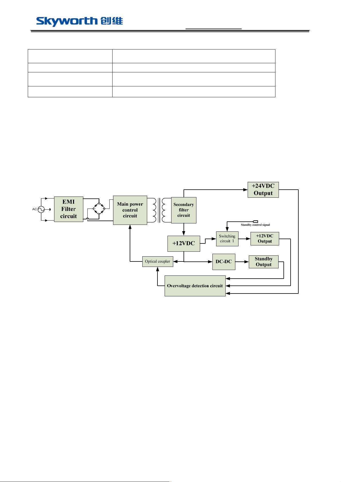
2.Circuit description)
2.1 The power circuit diagram
2.2 Each part of the circuit description
2.2.1 the main part of the circuit):NXP TEA1733P
2
Page 6

168P-P32ELL-W1 Service manual
3. The main chip description
3.1 The main chip
3.1.1 The main chip general description
The main chip of power supply is the TEA1733P which is produced by NXP corporation.
The operating mode is CCM (continuous conduction mode), and the operating frequency is
65KHz.
3.1.2 The chip pin information
3
Page 7

3.1.3 The chip block diagram
168P-P32ELL-W1 Service manual
3.1.4 The IC pin description
4
Page 8

168P-P32ELL-W1 Service manual
3.2 The DC-DC chip
3.2.1
frequency is 700KHz.
3.2.2
General description
The DC-DC used for standby chip, using SY8172Y, double synchronous rectification,and operating
The chip block diagram
3.2.3 The chip pin information
5
Page 9

168P-P32ELL-W1 Service manual
3.2.4 The pin description and the voltage
6
Page 10

168P-P32ELL-W1 Service manual
4. PCB TopOverlay and BottomOverlay
4.1 The power supply TopOverlay
4.2 The power supply BottomOverlay
7
Page 11

168P-P32ELL-W1 Service manual
5. Maintenance instructions
5.1 Common Fault Analysis and Notes
1.No +5VSB output voltage
If there is no +5VSB output voltage , we should focus on checking the DC-DC IC(IC301) and judge
whether the IC is operating . Monitor its VIN pin and check voltage is normal or abnormal . If it is normal ,
firstly , check the DC-DC IC peripheral circuit . Secondly, check DC-DC IC(IC301)and judge it has broken
or not. If the VIN pin voltage is abnormal, you need to check the IC100 power circuits.
2.+5VSB output is normal ,+12V output is abnormal
First, check +12 V voltage of the MOS transistor(Q300) S pole is normal or abnormal , if it is
normal,please check the MOS transistor(Q300) peripheral circuit is normal or not. If the +12 V voltage of
the MOS transistor(Q300) S pole is abnormal, please check the IC100 circuits.
3.+5VSB is abnormal
Check the +5 VSB feedback loop , and the reference voltage of the IC301 is normal or not.
8
Page 12

5.2 Service process
NO +5VSB
168P-P32ELL-W1 Service manual
Check + 5V output , Whether
the short-circuit
N
Is IC301 damaged?
N
Examine the positive voltage
of C312: 11.8V-12.2V?
N
Is IC100 damaged?
Y
Y
Y
Examine the reason
Change the damaged component
Check the peripheral circuit of
IC301
Y
Change the damaged component
N
Y
Check the peripheral
circuit of IC100
N
Examine the reason a n d
Change the damaged component
Examine overvoltage detection
circuit:Q304 ZD304 ZD302
ZD303
& Change the damaged component
9
Page 13

168P-P32ELL-W1 Service manual
5.2 Port and the connection defined
5.2.1 PIN11 CN200 Connection And Function
NO. Pin Connection Function
1 GND GND
2 GND GND
3 24V +24VDC OUTPUT
4 24V +24VDC OUTPUT
5 24V +24VDC OUTPUT
6 GND GND
7 ADJ ADJ
8 ENA ENA
9 GND GND
10 5VSB +5VSB DC OUTPUT
11 ON/OFF POWER_ON/OFF
Note: CN200 TYPE : 2.5mm
5.2.2 PIN14
CN300 Connection And Function
NO.
1 +24V +24V DC OUTPUT
2 +24V +24V DC OUTPUT
3 GND GND
4 GND GND
5 +12V +12V DC OUTPUT
6 +12V +12V DC OUTPUT
7 GND GND
8 GND GND
9 +5VSB +5VSB DC OUTPUT
Pin Connection Function
10 GND GND
11 ON/OFF POWER_ON/OFF
12 GND GND
13 ADJ BL_ADJUST
14 ENA BL_ON/OFF
Note: CN300 TYPE : 2.5mm
10
Page 14

168P-P32ELL-W1 Service manual
5.3 Key components and service parts list
Material
NO. Material number
models
1 4706-B17330-0080 TEA1733P IC100
2 47EC-S81721-0080 SY8172Y IC301
3 4600-P27610-00
4 4500-210200-0000
5 5132-064955-0000
6 47AH-P817C0-04 BPC-817C0 IC101
AOTF10N65
HBR10200HF
SANHE-42-102
Position
number
Q201
D301
D302
T101
Function
Main chip
DC-DC chip
Main MOS
Secondary
Schottky
transformer
Optocoupler
Substitute
Material
5.4 Storage, transportation and using conditions
5.4.1 Package
Box must have the product name, model, identification,quality inspection department certification,the
date of manufacture and so on.
Remar
k
5.4.2 Transportation
The productor adapted to cars, boats, aircraft transport .Transportation should be covered, prevented
sunshine and loading lightly.
5.4.3 Storage
Products should be stored in a box if it is not used .The storehouse environment temperature is from
-40 ℃ to -55 ℃, relatived humidity is from 10% to -95%. The storehouse must not allow any harmful
gases, flammable ,explosive and corrosive product chemicals, and must not allow strong mechanical
vibration, shock and strong magnetic field. Boxes should be at least 20cm high from the ground .The
distance from the wall, heat source, windows or air enter is at least 50cm. The storage period is about two
years, more than two years should be re-tested under the regulation .
11
Page 15

168P-P32ELL-W1 Service manual
6.Information of Power supply designers
Team Ⅱ Power Supply,R&D Center
Hu Xiangfeng and Zhou Cong
Email: huxiangfeng@skyworth.com
zhoucong@skyworth.com
12
Page 16

7. Schematic diagram
D101
VDR101
D102
213
2008*4
D104
-+
D103
4
C102
C101
472/1KV
472/1KV
LF102
1 2
3 4
CX102
471/400VAC
1 2
3 4
LF101
224/275VAC
N
CN101
10MH
10MH
CX101
TNR101
CY102
471/400VAC
2M/1/4W
2M/1/4W
123
L
R104
R102
R106
A2
R201
10K/1/4W
F101
FUSE T3.15A 250VAC
R105
100R/2W
474/275VAC
CY101
A1
R103
2M/1/4W
R101
2M/1/4W
TH101
5.0
C104
C103
+
+
68U 450V
68U 450V
R203A
R203
10M/1/2W
R202
10M/1/2W
10M/1/2W
R204
R202A
10M/1/2W
C202
ZD206
R216
27V
R217
200K/1/6W
C204
D201
IN4007
100R/2W
D202
IN4007
VDR102
ZD204
27V
168P-P32ELL-W1 Service manual
C301
102/1KV
SB10200
D301
D302
SB10200
102/1KV
R301
22R/1W
L301
5UH
C302
+
C303
104
1000U 35V
C305
R302
22R/1W
C310
C311
C309
+
+
104
1000UF25V
R312
220/1/4W
R314
1K/1/6W
C320
R315
10K/1/6W
224
IC300
TL431
+
C304
1000U 35V
Q301
C307
104
8050
R305A
10K/1/6W
R303
R305
Q308
20K/1/6W
2K/1/6W
L302
5uH
1000uF/25V
R313A
NC
4.7K/1/6W
PNP
+
C312
Q300
1000uF/25V
60N04
R313
R319
18K/1/6W
10k
C327
C328
R326
4.7K/1/6W
10UF
10uF
R316
R316A
NC
R310
R309
4.7K/1/6W
R328
10K/1/6W
1K/1/6W
Q303
PNP
Q302
PNP
R308
R300
1K/1/6W
500R/5W
ZD301
15V
D303
LL4148
R320
100k
R323
18k
R327
+12V/2A
+5V/0.5 A
C321
C332
+
22uF
R311
4.7K/1/6W
100uF/16V
ZD304
6V2
D305
LL4148
4.7K/1/6W
R304
20K/1/6W
PS_ON
2K/1/6WR306
+
C308A
NC
R307
10K/1/6W
+
C314
ZD302
1000uF/25V
27V
C323
103
R317
0R
IC301
IN
BST
2
5
L303
SW
6
FBEN
15uF
SY8172Y
8
1
4
C322
GND
220PF
ZD303
15V
D304
LL4148
R323A
62k
Q304
8050
C330
104
C210
R210
103/630V
100K 2W
D205
BA158
Q201
D206
2761
LL4148
R209
10K/1/6W
R207
R208
470K/1/4W
IC100
TEA1733
5
Visense
104
6
Protect
C203
7
104
8
Optimer
10K/1/6W
C205
R206
1M/1/6W
224
102
33R/1/6W
10R/1/6W
ZD205
R211
4
Isense
1K/1/6W
3
Driver
C206
102
GND2CTRL
1
VCC
C207
104
18V
R212
ZD202
33K/1/6W
C208
5V6
224
D207
BA158
+
ZD201
C209
27V
10U 50V
ZD203
SPECIFICATION
INPUT: 90-264V AC
+24V/2A
OUTPUT:
+12V/3A
+5VSB/0.5A
R213
0.18/2W
6R8/1/4W
R215
T101
9
10
7
8
15
16
5
1
11
2
12
13
CY105
222/400VAC
IC101
PC817C
1
4
27V
23
13
 Loading...