

查询PLL520-38OC-R供应商
PLL520-38/-39
PECL and LVDS Low Phase Noise VCXO (for 65-130MHz Fund Xtal)
FEATURES
• 65MHz to 130MHz Fundamental Mode Crystal.
• Output range: 65MHz – 130MHz (no PLL).
• Low Injection Power for crystal 50uW.
• PECL (PLL520-38) or LVDS output (PLL520-39).
• Integrated variable capacitors.
• Supports 2.5V or 3.3V-Power Supply.
• Available in 16-Pin (TSSOP or 3x3 QFN).
DESCRIPTION
The PLL520-38/-39 is a family of VCXO IC’s
specifically designed to pull high frequency
fundamental crystals from 65MHz to 130MHz, with
selectable PECL or LVDS outputs.. They achieve
very low current into the crystal resulting in better
overall stability. Their internal varicaps allow an on
chip frequency pulling, controlled by the VCON
input. Their very low jitter makes them ideal for the
most demanding timing requirements.
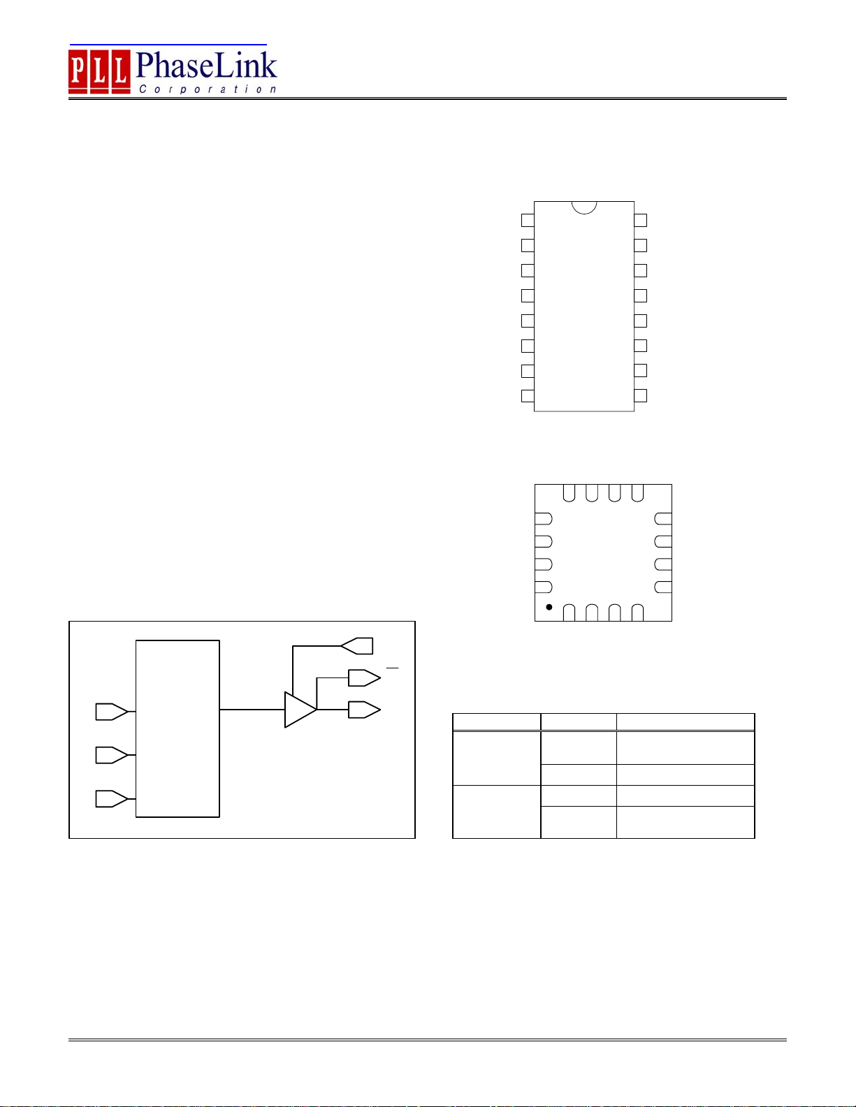
BLOCK DIAGRAM
PIN CONFIGURATION
VDD
P520-3x
16
15
14
13
12
11
10
9
N/C
VDD
XIN
XOUT
N/C
N/C
OE
VCON
GND
XOUT
XIN
N/C
OE
1
2
PLL 520-3x
3
4
5
6
7
8
VDD
12 11 10 9
13
14
15
16
123
4
N/C
8
7
6
5
N/C
N/C
GND
CLKC
VDD
CLKT
N/C
N/C
GND
CLKC
VDD
CLKT
VCON
XIN
Oscillator
Amplifier
w/
integrated
varicaps
OE
Q
Q
OUTPUT ENABLE LOGICAL LEVELS
Part # OE State
PLL520-38
XOUT
PLL520-38/-39
PLL520-39
OE input: Logical states defined by PECL levels for PLL520-38
47745 Fremont Blvd., Fremont, California 94538 Tel (510) 492-0990 Fax (510) 492-0991 www.phaselink.com Rev 09/20/04 Page 1
Logical states defined by CMOS levels for PLL520-39
GND
GND
VCON
0
(Default)
GND
Output enabled
1 Tri-state
0 Tri-state
1
(Default)
Output enabled

PLL520-38/-39
PECL and LVDS Low Phase Noise VCXO (for 65-130MHz Fund Xtal)
PIN DESCRIPTIONS
Name Number Type Description
XIN 2 I Crystal input. See Crystal Specifications on page 2.
XOUT 3 I Crystal output. See Crystal Specifications on page 2.
OE 6 I Output enable. See Output Enable Logic table on page 1.
VCON 7 I Voltage control input.
GND 8, 14 P Ground.
CLKT 11 O True output PECL (PLL520-38) or LVDS (PLL520-39).
CLKC 13 O Complementary output PECL (PLL520-38) or LVDS (PLL520-39).
N/C 4,5,9,10,15,16 - Not connected.
VDD 1, 12 P Power supply.
ELECTRICAL SPECIFICATIONS
1. Absolute Maximum Ratings
PARAMETERS SYMBOL MIN. MAX. UNITS
Supply Voltage VDD 4.6 V
Input Voltage, dc VI -0.5 VDD+0.5 V
Output Voltage, dc VO -0.5 VDD+0.5 V
Storage Temperature TS -65 150
Ambient Operating Temperature* TA -40 85
Junction Temperature TJ 125
Lead Temperature (soldering, 10s) 260
ESD Protection, Human Body Model 2 kV
Exposure of the device under conditions beyond the limits specified by Maximum Ratings for extended periods may cause permanent damage to the
device and affect product reliability. These conditions represent a stress rating only, and functional operations of the device at these or any other
conditions above the operational limits noted in this specification is not implied.
* Note: Operating Temperature is guaranteed by design for all parts (COMMERCIAL and INDUSTRIAL), but tested for COMMERCIAL grade only.
°C
°C
°C
°C
2. Crystal Specifications
PARAMETERS SYMBOL CONDITIONS MIN. TYP. MAX. UNITS
Built-in Capacitance
Inter-electrode capacitance C0
C0/C1 ratio (gamma)
Oscillation Frequency OF Fund. 65 130 MHz
CX+ 2
CX- 2
γ
65MHz to 130MHz
(VDD=3.3V)
300 -
pF
2.6
47745 Fremont Blvd., Fremont, California 94538 Tel (510) 492-0990 Fax (510) 492-0991 www.phaselink.com Rev 09/20/04 Page 2

PLL520-38/-39
PECL and LVDS Low Phase Noise VCXO (for 65-130MHz Fund Xtal)
3. Voltage Control Crystal Oscillator (3.3V)
PARAMETERS SYMBOL CONDITIONS MIN. TYP. MAX. UNITS
VCXO Stabilization Time * T
VCXO Tuning Range
From power valid 10 ms
VCXOSTB
F
= 100 – 200MHz;
XIN
XTAL C
0/C1
< 250
200* ppm
0V ≤ VCON ≤ 3.3V
CLK output pullability
On-chip Varicaps control range
VCON=1.65V, ±1.65V ±100*
VCON = 0 to 3.3V 4 – 18* pF
ppm
Linearity 10* %
VCXO Tuning Characteristic
VCON input impedance
VCON modulation BW
Note: Parameters denoted with an asterisk (*) represent nominal characterization data and are not production tested to any specific limits.
65 ppm/V
60
0V ≤ VCON ≤ 3.3V, -3dB
25 kHz
kΩ
4. General Electrical Specifications
PARAMETERS SYMBOL CONDITIONS MIN. TYP. MAX. UNITS
Supply Current (Loaded
Outputs)
Operating Voltage V
Output Clock Duty Cycle
Short Circuit Current
I
DD
DD
PECL/LVDS 100/80 mA
2.97 3.63 V
@ 1.25V (LVDS)
@ V
– 1.3V (PECL)
DD
45
45
50
50
±50
55
55
%
mA
5. Jitter Specifications
PARAMETERS CONDITIONS MIN. TYP. MAX. UNITS
Period jitter RMS 77.76MHz 2.5 ps
Period jitter peak-to-peak 77.76MHz 18.5 ps
Integrated jitter RMS Integrated 12 kHz to 20 MHz at 77.76MHz 0.5 ps
6. Phase Noise Specifications
PARAMETERS FREQUENCY @10Hz @100Hz @1kHz @10kHz @100kHz UNITS
Phase Noise relative
to carrier
Note: Phase Noise measured at VCON = 0V
77.76MHz -75 -95 -125 -145 -155 dBc/Hz
47745 Fremont Blvd., Fremont, California 94538 Tel (510) 492-0990 Fax (510) 492-0991 www.phaselink.com Rev 09/20/04 Page 3
PLL520-38/-39
PECL and LVDS Low Phase Noise VCXO (for 65-130MHz Fund Xtal)
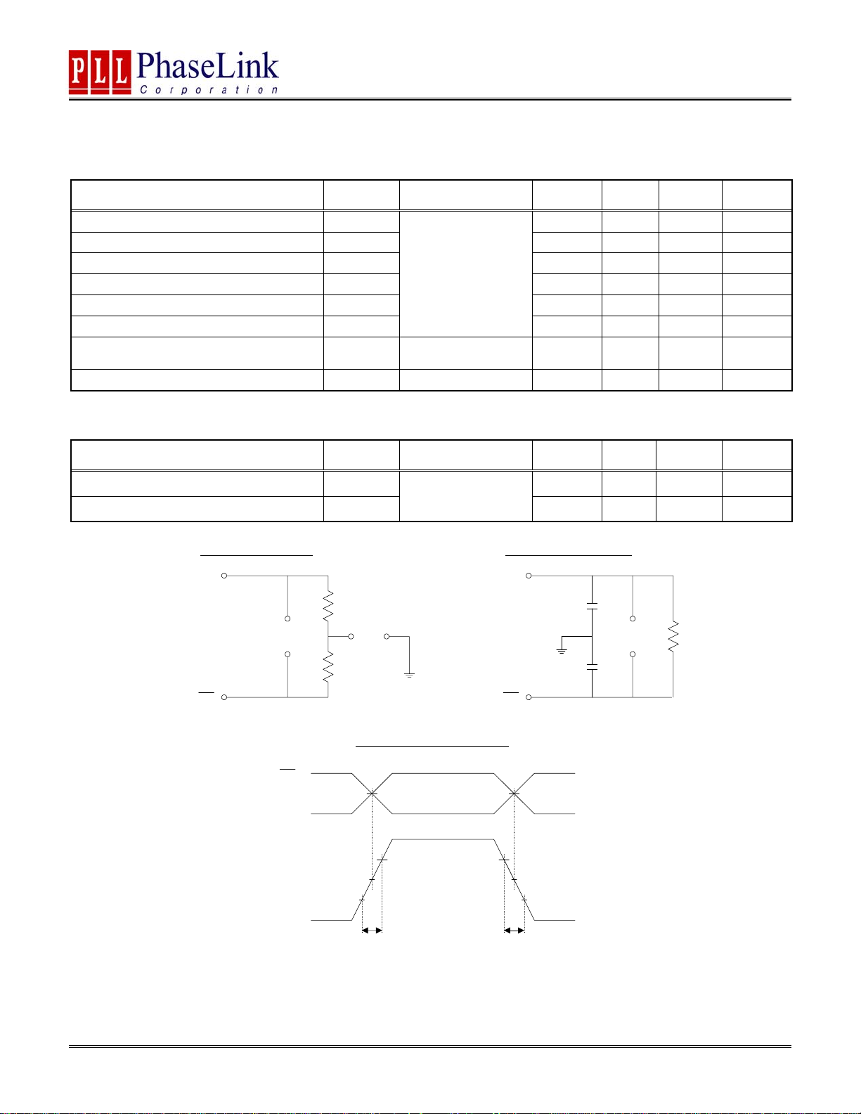
7. LVDS Electrical Characteristics
PARAMETERS SYMBOL CONDITIONS MIN. TYP. MAX. UNITS
Output Differential Voltage VOD 247 355 454 mV
VDD Magnitude Change
Output High Voltage VOH 1.4 1.6 V
Output Low Voltage VOL 0.9 1.1 V
∆V
OD
R
= 100 Ω
L
(see figure)
Offset Voltage VOS 1.125 1.2 1.375 V
Offset Magnitude Change
Power-off Leakage I
Output Short Circuit Current I
∆V
OS
V
= VDD or GND
OXD
-5.7 -8 mA
OSD
out
V
DD
= 0V
8. LVDS Switching Characteristics
PARAMETERS SYMBOL CONDITIONS MIN. TYP. MAX. UNITS
-50 50 mV
0 3 25 mV
±1 ±10
uA
Differential Clock Rise Time t
Differential Clock Fall Time t
OUT
OUT
V
OUT
OUT
V
OD
DIFF
r
f
50
Ω
V
OS
50
Ω
LVDS Transistion Time Waveform
0V (Differential)
80%
0V
20%
RL = 100 Ω
C
= 10 pF
L
(see figure)
80%
LVDS Switching Test CircuitLVDS Levels Test Circuit
OUT
OUT
0.2 0.7 1.0 ns
0.2 0.7 1.0 ns
CL = 10pF
20%
C
= 10pF
L
V
DIFF
RL = 100
Ω
t
R
t
F
47745 Fremont Blvd., Fremont, California 94538 Tel (510) 492-0990 Fax (510) 492-0991 www.phaselink.com Rev 09/20/04 Page 4

PLL520-38/-39
PECL and LVDS Low Phase Noise VCXO (for 65-130MHz Fund Xtal)
9. PECL Electrical Characteristics
PARAMETERS SYMBOL CONDITIONS MIN. MAX. UNITS
Output High Voltage VOH V
Output Low Voltage VOL
R
= 50 Ω to (VDD – 2V)
L
(see figure)
– 1.025 V
DD
V
– 1.620 V
DD
10. PECL Switching Characteristics
PARAMETERS SYMBOL CONDITIONS MIN. TYP. MAX. UNITS
Clock Rise Time t
Clock Fall Time t
r
f
@20/80% - PECL 0.6 1.5 ns
@80/20% - PECL 0.5 1.5 ns
PECL Levels Test Circuit
OUT
50
Ω
50
Ω
OUT
VDD
2.0V
PECL Transistion Time Waveform
DUTY CYCLE
PECL Output Skew
OUT
50%
OUT
t
SKEW
45 - 55% 55 - 45%
OUT
80%
50%
20%
OUT
t
R
t
F
47745 Fremont Blvd., Fremont, California 94538 Tel (510) 492-0990 Fax (510) 492-0991 www.phaselink.com Rev 09/20/04 Page 5
PLL520-38/-39
PECL and LVDS Low Phase Noise VCXO (for 65-130MHz Fund Xtal)
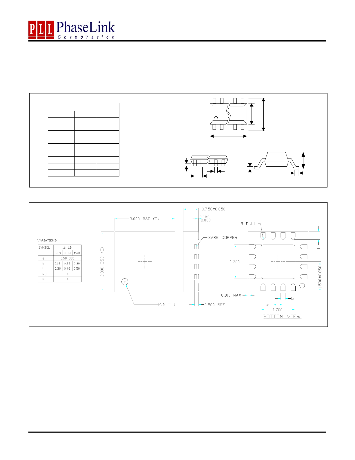
PACKAGE INFORMATION
16 PIN TSSOP ( mm )
Symbol Min. Max.
A - 1.20
A1 0.05 0.15
B 0.19 0.30
C 0.09 0.20
D 4.90 5.10
E 4.30 4.50
H 6.40 BSC
L 0.45 0.75
e 0.65 BSC
A1
e
D
B
EH
A
C
L
3x3mm QFN
47745 Fremont Blvd., Fremont, California 94538 Tel (510) 492-0990 Fax (510) 492-0991 www.phaselink.com Rev 09/20/04 Page 6

PLL520-38/-39
PECL and LVDS Low Phase Noise VCXO (for 65-130MHz Fund Xtal)
ORDERING INFORMATION
For part ordering, please contact our Sales Department:
47745 Fremont Blvd., Fremont, CA 94538, USA
Tel: (510) 492-0990 Fax: (510) 492-0991
PART NUMBER
The order number for this device is a combination of the following:
Device number, Package type and Operating temperature range
PLL520-3x O C
PART NUMBER
TEMPERATURE
C=COMMERCIAL
I=INDUSTRAL
PACKAGE TYPE
O=TSSOP Q=QFN
Order Number Marking Package Option
PLL520-38OC P520-38OC TSSOP - Tube
PLL520-38OC-R P520-38OC TSSOP - Tape & Reel
PLL520-38QC P520-38QC QFN - Tube
PLL520-38QC-R P520-38QC QFN - Tape & Reel
PLL520-39OC P520-39OC TSSOP - Tube
PLL520-39OC-R P520-39OC TSSOP - Tape & Reel
PLL520-39QC P520-39QC QFN - Tube
PLL520-39QC-R P520-39QC QFN - Tape & Reel
PhaseLink Corporation, reserves the right to make changes in its products or specifications, or both at any time without notice. The information
furnished by Phaselink is believed to be accurate and reliable. However, PhaseLink makes no guarantee or warranty concerning the accuracy of said
information and shall not be responsible for any loss or damage of whatever nature resulting from the use of, or reliance upon this product.
LIFE SUPPORT POLICY: PhaseLink’s products are not authorized for use as critical components in life support devices or systems without the
express written approval of the President of PhaseLink Corporation.
47745 Fremont Blvd., Fremont, California 94538 Tel (510) 492-0990 Fax (510) 492-0991 www.phaselink.com Rev 09/20/04 Page 7
 Loading...