

Page 1

VCT-V, VCU-V, VCD-V
GRAPHICS BOARDS
USER'S MANUAL
Copyright (c) 1995 by
Peritek Corporation
5550 Redwood Road
Oakland, CA 94619
(510) 531-6500
FAX (510) 530-8563
email: [email protected]
Release 2.3
April 19, 1995
Applies to:
VCT-V FAB REV 4 and up
VCU-V FAB REV 4 and up
VCD-V FAB REV 2 and up
Page 2

Peritek
Page 3

Peritek
Page 4

Table of Contents
Introduction......................................................................................................................i-1
The Organization of This Manual ................................................................................................i-1
Getting Help.................................................................................................................................i-2
Manual Revisions.........................................................................................................................i-2
Notices .........................................................................................................................................i-3
Conventions Used In This Manual...............................................................................................i-4
Chapter 1 General Information .......................................................................................1-1
1.1 Introduction...........................................................................................................................1-1
1.2 Functional Description ..........................................................................................................1-2
Special Features of the VCU-V......................................................................................1-3
Special Features of the VCT-V......................................................................................1-3
Special Features of the VCD-V......................................................................................1-3
TMS 34020 Graphics Processor ....................................................................................1-3
TMS 34082 Floating Point Coprocessor.......................................................................1-4
Video RAM....................................................................................................................1-4
34020 Processor Memory (DRAM and PROM)............................................................1-5
Display Features.............................................................................................................1-5
VMEbus Interface..........................................................................................................1-6
Peripheral Support .........................................................................................................1-7
1.3 Additional References ...........................................................................................................1-8
1.4 General Specifications...........................................................................................................1-9
1.5 Monitor Requirements...........................................................................................................1-16
1.6 Configuration Information.....................................................................................................1-16
Chapter 2 Installing Your Peritek Graphics Board .........................................................2-1
2.1 Introduction...........................................................................................................................2-1
2.2 Unpacking Your Board .........................................................................................................2-2
2.3 VMEbus Installation .............................................................................................................2-3
2.3.1 Default Interrupt Settings on Peritek Video Boards.............................................2-3
2.3.2 Checking Board Addresses..................................................................................2-4
2.3.3 Installing the Graphics Board...............................................................................2-5
Figure 2-1 Example VMEbus Backplane ......................................................2-6
2.3.4 What's Next? ........................................................................................................2-7
2.3.5 Connecting the Mouse, Keyboard, and Console ..................................................2-8
2.3.6 Checking your Display.........................................................................................2-9
Figure 2-2 Jumper Locations for the VCT-V and VCU-V........................................................2-10
Figure 2-3 Jumper Locations for the VCD-V............................................................................2-11
2.4 Option Selection....................................................................................................................2-12
2.4.1 CSR Addresses.....................................................................................................2-12
2.4.2 Interrupt Grant Receive/Acknowledge.................................................................2-13
2.4.3 Interrupt Priority ..................................................................................................2-14
Page 5

Peritek
Page 6

Peritek
Page 7

Peritek
2.4.4 Flash EEPROM....................................................................................................2-15
2.4.5 Autoboot Enable ..................................................................................................2-15
VCD Autoboot Enable.....................................................................................2-15
VCT-V and VCU-V Autoboot Enable.............................................................2-15
2.4.6 DRAM and VRAM Size ......................................................................................2-16
2.4.7 Master Pixel Clock Oscillator Frequency ............................................................2-17
2.4.8 Interlaced Operation and VCU-V Slow Mode .....................................................2-18
2.4.9 BT482 Output Level (VCD-V/T - special order only).........................................2-18
2.4.10 Selecting PTERM Options.................................................................................2-19
2.4.11 Selecting Serial I/O Options...............................................................................2-20
2.5 Connections to the VCU-V, VCT-V, and VCD-V................................................................2-22
2.5.1 Console, Mouse, Trackball, and Keyboard Connectors.......................................2-23
2.5.1a Console...............................................................................................................2-23
2.5.1b Mouse and Trackball..........................................................................................2-24
2.5.1c Serial and PC Keyboards....................................................................................2-26
2.5.2 Video Connector..................................................................................................2-27
2.5.3 High Speed Data Port (HSP)................................................................................2-28
2.5.4 8-bit SCSI Port (VCT-V and VCU-V).................................................................2-29
2.5.5 Digital Video Connector (VCD-V only)..............................................................2-30
Chapter 3 Software Summary.........................................................................................3-1
3.1 Introduction...........................................................................................................................3-1
3.2 Software Availability by Platform and OS ............................................................................3-2
3.3 Write Posting.........................................................................................................................3-3
3.4 PX Windows Server ..............................................................................................................3-4
3.5 Graphics Subroutine Package................................................................................................3-5
3.6 PTERM Terminal Emulator..................................................................................................3-8
3.7 Software Development Package............................................................................................3-9
Features of the 34020 Development Tools ....................................................................3-10
3.8 Ancillary Programs................................................................................................................3-11
3.8.1 Initialization Tables .............................................................................................3-11
3.8.2 Software Installation Examples............................................................................3-11
3.8.3 VCnVINT ............................................................................................................3-12
3.8.4 VCnVTST............................................................................................................3-12
3.8.5 VCnVLD..............................................................................................................3-14
3.8.6 VCnVWT.............................................................................................................3-14
3.8.7 VCnVHLT ...........................................................................................................3-14
3.8.8 VCnVGO .............................................................................................................3-14
3.8.9 VCnVOFF............................................................................................................3-15
3.8.10 VCnVDMP ........................................................................................................3-15
3.8.11 TIDTSK .............................................................................................................3-15
Chapter 4 Theory of Operation .......................................................................................4-1
4.1 Introduction...........................................................................................................................4-1
4.2 System Architecture ..............................................................................................................4-2
VMEbus Interface..........................................................................................................4-2
Control Registers ...........................................................................................................4-2
Page 8

Peritek
34020/VMEbus Host Interface ......................................................................................4-3
34020 Functional Unit ...................................................................................................4-3
34020 Data and Address Buses......................................................................................4-3
4.3 Graphics Board Clock Sources..............................................................................................4-4
Phase Locked Loop (PLL) Clock...................................................................................4-4
34020 Video and Processor Clock Synchronization......................................................4-5
4.4 VMEbus Interface.................................................................................................................4-5
Address Decoding..........................................................................................................4-5
Data Bus Transceivers and the Byte Swapper................................................................4-6
4.5 VMEbus Interrupt Controller................................................................................................4-7
4.6 System Arbitration ................................................................................................................4-7
Control Register Decoding (CSRREQ)..........................................................................4-8
Line Buffer Decoding (IOREQ).....................................................................................4-8
34020 Host Interface Arbitrator.....................................................................................4-9
VMEbus Block Mode ....................................................................................................4-9
4.7 Display Memory....................................................................................................................4-9
VCD-V and VCU-V Pixel Size......................................................................................4-10
VCT-V Pixel Size..........................................................................................................4-10
VCD-V Display Memory Size.......................................................................................4-10
VCU-V Display Memory Size.......................................................................................4-10
VCT-V Display Memory Size........................................................................................4-11
4.8 System Memory.....................................................................................................................4-11
SIMM Sockets ...............................................................................................................4-11
Flash EEPROM..............................................................................................................4-11
4.9 Programmed Logic Devices ..................................................................................................4-12
AMD MACH Field Programmable Gate Arrays (FPGA)..............................................4-12
PAL22V10 Field Programmable Gate Array (FPGA) ...................................................4-12
Chapter 5 Programming On-board Devices and Memories............................................5-1
5.1 Introduction...........................................................................................................................5-1
5.2 VMEbus and Control Registers.............................................................................................5-3
5.2.1 Control/Status Register (CSR) .............................................................................5-4
5.2.2 Line Address Register (LAR) ..............................................................................5-6
5.2.3 A32 Address Map and the XARADR Address Match Register...........................5-8
5.2.4 A16/A24 Address Map and DBRADR Address Match Register.........................5-9
5.2.5 VECADR Interrupt Vector Address Register ......................................................5-10
5.2.7 VMEbus Block Transfers (BLT) .........................................................................5-11
5.2.8 Device Register Access........................................................................................5-11
5.3 TMS 34020 Graphics Systems Processor..............................................................................5-14
5.3.1 34082 Floating Point Coprocessor.......................................................................5-15
5.3.2 Writemask Register..............................................................................................5-15
5.3.3 VRAM Color Register and Block Fill Special Function......................................5-16
5.3.4 Memory Types and Sizes.....................................................................................5-17
5.3.5 Byte Ordering and the Hardware Byte Swapper ..................................................5-17
5.3.5a VMEbus and 34020 Byte Order Mapping .........................................................5-18
5.3.5b Example Code for Software Byte Swapping......................................................5-19
Page 9

Peritek
5.3.5c The Hardware Byte Swapper .............................................................................5-19
5.3.6 Virtual Memory, Page Faults, and Autoincrement Registers ...............................5-20
5.3.7 34020 Memory and Device Addresses.................................................................5-20
5.3.8 Sample Address Calculations...............................................................................5-22
5.4 Initialization Tables...............................................................................................................5-27
5.4.1 Application Note: Tweaking 34020 Initialization Parameters .............................5-31
Request for Timing Table................................................................................5-34
5.5 Vertical and Horizontal Zoom...............................................................................................5-35
Vertical Zoom................................................................................................................5-35
Horizontal Zoom............................................................................................................5-35
5.5.1 ICS1562 Type Horizontal Zoom Register ...........................................................5-36
5.5.2 VCD-V/A6 Type ICS1562 Version Horizontal Zoom Register...........................5-37
5.5.3 VCD-V/A6/D8 Type ICS1562 Version Horizontal Zoom Register.....................5-38
5.5.4 Horizontal Zoom Control Register (Non-ICS1562 VCD-V's).............................5-39
5.6 BT463 - Color Map Controller for the VCT-V.....................................................................5-43
5.7 BT468 - Color Map Controller for the VCU-V.....................................................................5-47
5.8 BT459 - Color Map Controller for the VCD-V.....................................................................5-50
5.9 BT482 - Color Map Controller for the VCD-V.....................................................................5-53
5.10 VCD-V Digital Lookup Table (DLUT) ..............................................................................5-57
5.11 Hardware Cursors................................................................................................................5-61
5.12 Serial I/O Ports (DUART)...................................................................................................5-64
5.13 SCSI Port.............................................................................................................................5-66
5.14 PC Keyboard Controller (8242PC) .....................................................................................5-69
5.15 High Speed Data Port (HSP)...............................................................................................5-69
5.16 Graphics Board Interrupts...................................................................................................5-72
5.17 Flash EEPROM and Serial EEPROM.................................................................................5-73
Chapter 6 Troubleshooting .............................................................................................6-1
6.1 Introduction...........................................................................................................................6-1
6.2 Selecting an Address Range for your Board..........................................................................6-2
Memory Map Example ..................................................................................................6-4
6.3 Does this board talk at all? ....................................................................................................6-5
6.4 General Procedures ...............................................................................................................6-7
6.6 Maintenance, Warranty, and Service.....................................................................................6-9
Maintenance...................................................................................................................6-9
Warranty ........................................................................................................................6-9
Return Policy .................................................................................................................6-9
Out of Warranty Service ................................................................................................6-9
Page 10

Peritek
Page 11

Introduction
This introductory chapter contains information about the organization of
this manual, how to get technical support, and the typographical
conventions used throughout the manual.
The Organization of This Manual
This manual provides information about how to configure, install, and
program the Peritek 34020-based VMEbus graphics controllers. Products
covered include the VCU-V ultra-high resolution controller, the VCT-V
24-bit true-color controller, and the VCD-V analog/digital controller. The
boards can be covered in one manual because their feature set is largely
the same, and the software is identical.
This manual is broken down into six chapters:
Chapter 1: Overview of the Peritek graphics boards
Chapter 2: Installing Peritek graphics boards
Chapter 3: Summary of Peritek's Software Products
Chapter 4: Theory of Operation
Chapter 5: Programming On-board Devices and Memories
Chapter 6: Troubleshooting
Chapter 1 provides interesting background material about Peritek graphics
boards. Understanding the information in the chapter, however, is not
essential for the hardware or software installation.
If you want to perform the installation as quickly as possible, start with
Chapter 2. If you have problems installing the hardware, refer to Chapter 6
for help.
Introduction-1
Page 12

Peritek
Getting Help
This installation manual gives specific steps to take to install your Peritek
graphics board. There are, however, variables specific to your computer
configuration and monitor that this manual cannot address. Normally, the
default values given in this manual will work. If you have trouble
installing or configuring your system, first read Chapter 6,
"Troubleshooting". If this information does not enable you to solve your
problems, do one of the following:
1) call Peritek technical support at (510) 531-6500,
2) fax your questions to (510) 530-8563,
3) or send E-mail to [email protected].
If your problem is monitor related, Peritek technical support will need
detailed information about your monitor.
Manual Revisions
Revision 2.0 January 11, 1995 First Word for Windows 2.0 Master
Revision 2.1 March 27, 1995 Compensate for WFW bug which
Revision 2.2 April 6, 1995 Fixed cursor address error in Ch. 5.
Revision 2.3 April 19, 1995 Fixed some format errors. Changed
yielded incorrect Table of Contents
and Index page numbers, fix minor
factual errors in Chapter 1.
the pagination style.
Introduction-2
Page 13

Peritek
Notices
Information contained in this manual is disclosed in confidence and may
not be duplicated in full or in part by any person without prior approval of
Peritek Corporation. Its sole purpose is to provide the user with adequately
detailed documentation to effectively install and operate the equipment
supplied. The use of this document for any other purpose is specifically
prohibited.
The information in this document is subject to change without notice. The
specifications of the VCU-V, VCD-V, VCT-V, and other components
described in this manual are subject to change without notice. Although it
regrets them, Peritek Corporation assumes no responsibility for any errors
or omissions that may occur in this manual.
Peritek Corporation assumes no responsibility for the use or reliability of
software or hardware that is not supplied by Peritek, or which has not been
installed in accordance with this manual.
PX Windows and Peritek are trademarks of Peritek Corporation. The
products, HP-UX, OS-9, pSOSystem, SunOS, OpenVMS, VAXeln,
Ultrix, VMEexec, V/68 SVR3, V/88 SVR3, and VxWorks are registered
trademarks of Hewlett-Packard, Microware, Integrated Systems, Sun,
DEC, DEC, DEC, Motorola, Motorola, Motorola, and Wind River,
respectively.
Copyright (c) 1994 by Peritek Corporation
Introduction-3
Page 14
Peritek
Conventions Used In This Manual
The following list summarizes the conventions used throughout this
manual.
Code
fragments
Code fragments, file, directory or path names and
user/computer dialogs in the manual are presented in the
courier typeface.
Commands or
program names
System prompts
and commands
Commands, or the names of executable programs, except
those in code fragments, are in bold.
Commands in code fragments are preceded by the system
prompt, a percentage sign (%), the standard prompt in UNIX's
C shell, a dollar sign ($), the OS-9 prompt, or the hash-mark
(#), the standard UNIX prompt for the Super-User.
Note Note boxes contain information either specific to one or more
platforms, or interesting, background information that is not
essential to the installation.
Caution Caution boxes warn you about actions that can cause damage
to your computer or its software.
Warning! Warning! boxes warn you about actions that can cause
bodily or emotional harm.
Keyboard usage <CR> stands for the key on your keyboard labeled
Introduction-4
“RETURN” or “ENTER”
Page 15

Chapter 1
General Information
1.1 Introduction
This chapter provides an overview of the VCT-V, VCD-V, and VCU-V
graphics controllers. Additional sections contain a bibliography,
specifications, monitor requirements, and common configurations.
This is summary information, and is not critical to the one who wishes to
press on to the installation procedures, which are contained in Chapter 2.
General Information 1-1
Page 16

Peritek
1.2 Functional Description
The Peritek VCD-V, VCT-V and VCU-V are based on the second
generation TMS 34020 32-bit Graphics System Processor (GSP). The
boards offer a high degree of on-board intelligence and functionality, as
well as a straightforward frame buffer interface.
The boards are differentiated chiefly by the bits/pixel of the primary
display memory and the video output sections. The VCD-V and VCU-V
have 8 bits/pixel in the primary plane and the VCT-V has 24-bits. The
VCU-V and VCT-V have only analog RGB outputs and the VCD-V offers
both analog and digital.
The common feature set of the VCU-V, VCT-V and VCD-V includes:
40 MHz 34020
Optional 34082 Floating Point Unit (FPU)
4 RS-232 serial I/O ports
PC Keyboard
4 Kb serial EEPROM
up to 2 MB autoboot Flash PROM
up to 32 MB 34020 memory
Optional multiple display pages
Hardware pan, zoom, and scroll
Hardware bitmapped cursors,
4 bit overlay
SIMMs for display and 34020 memory
PLL controlled pixel clock
genlock support for system wide synchronization
analog RGB video output
Up to 72 Hz display refresh rate
Optional 32-bit High Speed Data port
Optional autoboot simple console terminal emulator
BiCMOS bus transceivers and AMD MACH FPGAs
(for low power consumption)
Single 6U VMEbus board
Graphics Subroutine Package
X11R6 X Window System Server
1-2 General Information
Page 17

Peritek
Special Features of the VCU-V
The VCU-V has an 8-bit primary screen, an optional 8-bit SCSI port, and
up to two pages of 1600 x 1280 display. Programmable screen resolution
ranges from 640 x 480 pixels up to better than 1600 x 1280 with refresh
rates between 60 and 72 Hz vertical and 31 to 85 KHz horizontal refresh
rates non-interlaced.
Special Features of the VCT-V
The VCT-V supports displays up to 1280 x 1024, has a true color (24-bit)
primary screen, an optional 8-bit SCSI port, and up to four pages of 1280 x
1024 display. Programmable screen resolution ranges from 640 x 480
pixels up to 1280 x 1024 with refresh rates between 30 and 72 Hz vertical
and 15.7 to 73 KHz horizontal refresh rates, non-interlaced or noninterlaced, including NTSC sync compatible 640 x 483.
Special Features of the VCD-V
The VCD-V supports displays up to 1280 x 1024, has an 8-bit primary
screen, both analog and digital (flat panel) outputs (digital is limitied to
1024 x 768), simultaneous analog and dital operation (with VGA timing
compatible panels) and up to two pages of 1280 x 1024 display.
Programmable screen resolution ranges from 640 x 480 pixels up to 1280
x 1024 with refresh rates between 30 and 72 Hz vertical and 15.7 to 73
KHz horizontal refresh rates, non-interlaced or non-interlaced, including
NTSC sync compatible 640 x 483.
The VCT and VCU are also available in DEC compatible Q-Bus and
TURBOchannel versions.
TMS 34020 Graphics Processor
The TMS 34020 is a CMOS 32-bit processor with hardware support for
graphics operations such as PIXBLT and curve-drawing algorithms.
Included is a complete set of general purpose instructions with addressing
modes tuned to high level languages. In addition to addressing a 512 MB
external memory range, the 34020 contains 30 general purpose 32-bit
registers, stack pointer, and a 512 byte LRU instruction cache. On chip
functions include 64 programmable registers used for CRT timing, I/O
control, and instruction parameters. The 34020 can receive interrupts from
the the VMEbus, serial I/O, and SCSI.
General Information 1-3
Page 18

Peritek
The 34020 mediates all host accesses to display and processor memory
and control registers through a byte addressable 32 bit interface port. Bus
transceivers between the 34020 bus and VMEbus support D16 and D32
data transfers for the VMEbus.
The 34020 features single-cycle execution of general purpose instructions
and most common integer arithmetic and Boolean operations from
instruction cache. A 32-bit barrel shifter supports single cycle shift and
rotation for 1 to 32 bits.
The 34020 graphics processing hardware supports pixel and pixel-array
processing. It incorporates two and three operand raster operations with
Boolean and arithmetic operations, XY addressing, window clipping and
checking, 1 to n bits/pixel transforms, transparency, and plane masking.
Operations on single pixels (PIXT instruction) or two-dimensional arrays
(PIXBLT) are supported.
TMS 34082 Floating Point Coprocessor
For floating point intensive applications, a socket is provided for a 34082
FPU coprocessor. It conforms to the IEEE floating point standard 7541985 for binary floating point single or double precision addition,
subtraction, multiplication, division, square root, and comparison. In
addition, it offers 32-bit integer arithmetic, logical comparisons, and shifts.
Complex operations for graphics support include: matrix operations (1 x 3,
3 x 3, 1 x 4, and 4 x 4), backface testing, polygon elimination and clipping,
viewport scaling and conversion, 2D and 3D linear interpolation, 2D
window compare, 3D volume compare, 2 plane clipping (X, Y, Z), 2 plane
color clipping (R, G, B, I), 2D and 3D cubic splines, 3 x 3 convolution,
vector operations (add, subtract, dot and cross products, magnitude,
scaling, normalization and reflection), polynomial expansion,
multiply/accumulate, and 1D and 2D min/max.
Video RAM
The display memories use advanced 2 Mbit (256K x 8) 2-port Video RAM
(VRAM) technology, which gives approximately 95% memory availability
to the 34020 and host processors. A writemask register supports write
protection of bit planes.
The 34020 supports the VRAM accelerated functions such a block write
and fill with special VFILL and VBLT instructions. These can be used to
quickly replicate one and two dimensional patterns in memory, at up to 16
1-4 General Information
Page 19

Peritek
times the single pixel rate. On the VCD-V and VCU-V, up to sixteen 8-bit
pixels can written in each 100 ns page mode cycle, resulting in a 160
Mpixel/sec VFILL time. The VCT-V, which has 32-bit pixels, has a 40
Mpixel/sec VFILL time.
34020 Processor Memory (DRAM and PROM)
The 34020 has its own "system" memory, which is independent of the
video memory. However, it does share a common address space with the
display memory and can thus be used for program store or off-screen
display data. The standard size is 1 MB of 0 wait state DRAM, and is
expandable to 32 MB.
There are four 32-pin PLCC sockets which support up to 2 MB (using
29F020 devices) of 0 wait state Flash PROM. Jumpers can be installed
which cause the 34020 to automatically start executing from PROM on
power-up. An additional 512 byte serial EEPROM can be installed which
can be used by an PROM-based program to store information necessary at
power-up (such as initialization data). PROM sets can be ordered from
Peritek which include a simple console terminal emulator combined with
the graphics subroutine package or X11R6 X Windows server.
Display Features
All boards support binary vertical zoom (1, 2, 4, 8, 16, 32), horizontal
zoom (except some VCD-Vs), multi-pixel horizontal pan and vertical
smooth scroll.
For the VCD-V and VCU-V, the display memory data is directed to the
analog monitor via a Brooktree RAMDAC color map control chip which
provides a programmable 24 bit wide color map (8 bits each red, green,
and blue). The 8-bit pixel is used as an index into the lookup table, giving
256 colors out of a palette of 16.7 Million. A two bit cursor with a 64 x 64
x 2 bit map function is also included on chip.
For the VCT-V, the display memory data is directed to the analog monitor
via a Brooktree BT463 color map control chip which provides a
programmable 24 bit wide color map (8 bits each red, green, and blue).
The 24-bit pixel is used as an index into the lookup table, giving a full
16.7 Million colors. A two bit cursor with a 64 x 64 x 2 bit map function is
also included, but incorporated in separate BT431 cursor chips.
For all boards, additional color map entries are provided for the overlay
screen and cursors. Any plane can be blanked or blinked. The analog Red,
General Information 1-5
Page 20

Peritek
Green, and Blue signals from the RAMDAC are connected to a monitor
such as the Peritek CVM-19/E-7.
On the VCD-V (only) the display memory data is also directed to a
proprietary Digital LookUp Table (DLUT) which provides a
programmable 8-bit wide map. Depending on how the VCD-V is
configured, 1, 4, or 8 bit monochrome or 8-bit color (3 bits red, 3 bits
green, and 2 bits blue) can be supported. The VCL-V, available in May
1995, will support expanded 12 to 24 bit color map options. The eight
bit pixel is used as an index into the lookup table, giving 256 colors out of
a palette of 16.7 Million. A two bit cursor with a 64 x 64 x 2 bit map
function is also included. Additional color map entries are provided for the
overlay screen and cursors. Contact Peritek for information on what panels
are supported.
VMEbus Interface
The VMEbus host interface accesses Peritek graphics board memory and
on-board devices through four control registers and a 1 KB line buffer
which are located in VMEbus A16 space. The line buffer can also appear
in A24 space.
The CSR contains device interrupt enables, line buffer response enable,
and 34020 hardware reset. The LAR is a 16 bit register which maps a
portion of the address space of the graphics board into a 1 KB line buffer.
Two additional registers include programmable line buffer address,
interrupt vector address and programmable extended address (A32)
decoder. Access to the board through the A16 space provides a "lowest
common denominator" access mode which allows the board to be
compatible with any host CPU. In an A16 VMEbus system it is necessary
to "window" into on-board memory because it is so large (maximum
memory capacity on the board is more than 48 MB!) The 1 KB window is
actually an efficient way of doing this.
The graphics boards also have an 64 MB window in A32 VMEbus address
space which allows direct access to all on-board memory.
VMEbus D32 block transfers are supported for A16/A24 and A32 address
spaces, which allows up to 256 bytes to be transferred at high speed over
the VMEbus. Another performance feature for the boards is a hardware
byte swapper. When enabled, four 1KB buffers are mapped to the board
which provide unswapped, byte, word, and long swaps, respectively.
The board has a VMEbus interrupt controller which supports a vectored
interrupt from the 34020.
1-6 General Information
Page 21

Peritek
Peripheral Support
The graphics board has four asynchronous RS-232 data-leads-only serial
I/O ports. Ordinarily, the board is configured to support 3 channels (serial
mouse/trackball, LK401-type keyboard, and console port), with the I/O
lines for the fourth port being "stolen" to support RTS/CTS on the console
port. Each port can be programmed separately for transmit and receive
baud rates up to 38.4 Kb. Each receive buffer is quadruply buffered to
minimize the possibility of data overrun. Each channel has an internal
loopback mode for testing.
An 8242PC keyboard controller gives a PC-compatible keyboard port and
a PS/2 mini-DIN connector is used.
The VCU-V and VCT-V also have an optional 8 bit Small Computer
Systems Interface (SCSI) peripheral port.
All three designs can be supplied with a 32-bit High Speed Port (HSP)
which allows 32-bit data to read or written directly by the 34020 to/from
system or graphics memory.
The Peritek graphics boards are highly configurable for special
requirements. In order to ensure optimum performance at the lowest OEM
cost, please contact Peritek for quotes for customized feature sets.
General Information 1-7
Page 22

Peritek
1.3 Additional References
Peritek documentation includes User's Manuals, Graphics Subroutine
Package Manual, and Peritek PX Windows Server Installation and User's
Guide. Due to lack of demand, data sheet extracts are no longer included
as Appendices to the manual. They are available upon request. The
manufacturer sources of this information are:
TMS 34020 User's Guide Texas Instruments
Order # SPVU019 Customer Response Center
TMS 340 Math/Graphics Function Library 1-800-232-3200
Order # SPVU006
TMS 340 Assembly Language User's Guide
Order # SPVU004
TMS 340 Family Code Generation Tools
Order # SPVU020B
SCN2681 Dual Asynchronous Receiver- Philips Semiconductors
Transmitter (DUART) Data Sheet 811 E. Arques Avenue
Signetics Microprocessor Data Manual Sunnyvale, CA 94088-3409
1986, pages 2-189 to 2-208 800-234-7381
BTxxx Product Descriptions Brooktree Corporation
9950 Barnes Canyon Road
Product Data Book, 4th Edition San Diego, CA 92121
619-452-7580
NCR5380 SCSI Processor NCR Microelectronics
1988 Standard Products Data Book 1635 Aeroplaza Drive
pages 75 - 115 Colorado Springs, CO 80916
1-800-525-2252
VMEbus Specification VITA
10229 N. Scottsdale Road
Suite B
Scottsdale, AZ 85253
(602) 951-8866
Graphics Textbooks
Fundamentals of Interactive Computer Graphics
Addision Wesley, 1982. Foleyand Van Dam
Principles of Interactive Computer Graphics
McGraw-Hill, 1979 Newman and Sproull
1-8 General Information
Page 23

Peritek
1.4 General Specifications
Graphics Processor: 40 MHz TMS 34020 Graphics System Processor has a
complete instruction set 32-bit CPU, vector and pix-blt
functions, and programmable video timing.
Floating Point Unit: A socket is provided on the board for the companion 40
MHz TMS 34082 Floating-Point Unit (FPU) coprocessor,
which can accelerate floating-point intensive operations by
an order of magnitude.
Non-Display Memory: Memory is 1 MB of 32-bits/word, byte addressable, no-wait
state, dynamic RAM. This memory is in the same memory
space as the display memory, so it can hold program store
and off screen display data. It is expandable in steps of 4, 8,
16 and 32 MB. A minimum of 4 MB is required for PX
Windows.
PROM Memory: Four 8-bit Flash PROMs support no-wait state firmware
storage of up to 2 MB (total) of 32-bit wide permanent
storage. A user jumper allows the board to auto-start from
EPROM.
Peritek can supply dumb terminal emulation (PTERM),
Graphics Subroutine Package (CnP), and Peritek's PX
Windows X11R6 server in PROM. Possible combinations
are PTERM alone, CnP alone, PX Windows alone, or a
combination of PTERM and either CnP or PX Windows.
An optional 4 Kbit (512 byte) serial Electrically Eraseable
Programmable Read Only Memory (EEPROM),
programmed via DUART 0, supplies non-volatile readmostly memory for an EPROM-based application to retain
some changeable data during power down. Software
support for this function is under development.
General Information 1-9
Page 24

Peritek
Video Display: On the VCD-V and VCU-V, the display word size is 32
bits, and is divided into 1 byte per pixel. Overlay is
allocated a byte per pixel, but only the low 4 bits are valid.
The lookup table (LUT) resolves the display priority
between the primary, overlay, and cursor (last through first,
respectively) screens.
On the VCT-V, the display word size and pixel size is 32
bits. Bits 0-7 are Red, bits 8-15 are green, bits 16-23 are
blue, bits 24-27 are overlay, bits 28-29 are for window type
table, and bits 30-31 are read/write but not used. The
BT463 RAMDAC lookup table resolves the display priority
between the primary, overlay, and cursor (last through first,
respectively) screens.
Display Memory: The basic display memory size for the VCD-V is 1 MB of
32-bits/word, byte addressable, no-wait state, dual-port
Video RAM. This provides 1024 x 1024 x 8 bit/pixel
primary screen. Overlay may be specified at order time. The
display memory is expandable to 8 MB. The /2M option
can give either 1280 x 1024 displayable or two pages of
1024 x 1024 pixels. The /4M option can give two pages of
1280 x 1024 displayable or four pages of 1024 x 1024
pixels.
The basic display memory size for the VCU-V is 2 MB,
which provides 2048 x 1024 addressable pixels (8 bit/pixel
primary, 4 bit/pixel overlay). The memory is expandable to
16 MB. The /4M option gives one page of 1600 x 1280,
two pages of 1280 x 1024 or four pages of 1024 x 1024
pixels. The /8M option can give two pages of 1600 x 1280,
four pages of 1280 x 1024 or eight pages of 1024 x 1024.
The standard memory size for the VCT-V is 8 MB of 32bits/word, byte addressable, no-wait state, dual-port Video
RAM. This provides a 1280 x 1024 display size with 2048
x 1024 x 32 bit/pixel addressable pixels. The display
memory is expandable to 16 MB. The /4M option can give
one page of two pages of 1280 x 1024 or four pages of
1024 x 1024.
Writemask Register: A 32-bit Writemask register permits individual bits in
display memory to be write protected. This allows write
operations (as opposed to read-modify-write) on display
memory.
1-10 General Information
Page 25

Peritek
Pixel Clock: The VCU-V, VCT-V, and (optionally) the VCD-V utilize
an ICS 1562 PLL controlled user programmable pixel clock
generator. Most VCD-V configurations use a standard fixed
frequency oscillator.
Scroll, Pan, and Zoom: Scroll - single line (smooth scroll).
Pan - resolution depends on initialization and color map:
VCU-V: anywhere on 8 or 16 pixel boundaries.
VCT-V: anywhere on 4 or 8 pixel boundaries.
VCD-V: anywhere on 2, 4, or 8 pixel boundaries.
Zoom - vertical (1, 2, 4, 8, 16, 32) - horizontal
(depends on board type):
VCT-V and VCU-V: sub-integer, uses the ICS1562
to adjust master pixel clock.
VCD-V: BT459 color map based supports 1-16
BT482 and DLUT based has no zoom function
VCD-V Color Maps: The VCD-V analog output uses a Brooktree BT482
RAMDAC for low frequency (up to 1024 x 768) analog
displays. The BT482 contains a 32 x 32 x 2 bitmapped
cursor and works correctly with interlaced displays.
The VCD-V uses a Brooktree BT459 RAMDAC for high
frequency (above 1024 x 768) analog displays. The BT459
contains a 64 x 64 x 2 bitmapped cursor, which does not
work correctly with interlaced displays.
The VCD-V digital output consists of a 32K x 8 lookup
table (LUT) and a 32 x 32 x 2 bitmapped cursor controller.
8 bit primary, 4 bit overlay, and 2 bit cursor data are passed
through the LUT, which provides an 8 bit pixel output to
the digital output connector.
VCU-V Color Map: The VCU-V output uses a Brooktree BT468 RAMDAC for
displays ranging from 640 x 480 up to better more than
1600 x 1280 non-interlaced (only). The BT468 also
contains a 64 x 64 x 2 bitmapped cursor which does not
work correctly with interlaced displays.
VCT-V Color Map: The VCT-V output uses a Brooktree BT463 True Color
RAMDAC for displays ranging from 640 x 480 interlaced
up to better more than 1280 x 1024 non-interlaced. A
separate dual BT431 cursor contains both crosshair and a
64 x 64 x 2 bitmapped cursors and works correctly with
interlaced displays.
General Information 1-11
Page 26

Peritek
Serial I/O Ports: Four asynchronous serial I/O ports are contained in two
Signetics 2681 DUARTs. Each port can be programmed for
transmit and receive baud rates up to 38.4 Kb. Receive
buffers are quadruply buffered to minimize the possibility
of data overrun. Each DUART also contains a
programmable timer/counter. Ordinarily, one port is for a
serial mouse, one port is for the console (PTERM), one port
is for LK401-type keyboard. The I/O lines for the fourth
port are normally allocated as RTS/CTS for the console
port, but can be rejumpered as a serial port.
PC Keyboard Port: An Intel 82C42PC keyboard controller supports standard
PC keyboards (PTERM and PX Windows software support
available). Connection is made via a mini-DIN PS/2
connector.
SCSI Port: On the VCT-V and VCU-V an optional Small Computer
Systems Interface (SCSI) peripheral port, using an NCR
5380 controller, supports up to 7 high speed (1 MB/second)
8-bit parallel intelligent devices. It allows any compatible
device (such as a SCSI disk) to be used.
For improved performance, an alternate port address mode
allows the 34020 to utilize the 5380 pseudo-DMA mode,
which automatically operates the SCSI handshake lines
during data transfers.
Since the 5380 is highly programmable, the SCSI port may
also be used as an 8-bit parallel I/O port.
At this time, no direct software support is available for
the SCSI.
High Speed Port (HSP): A direct reading 32-bit port allows the 34020 to connect to
an external device and read data directly into memory at
page-mode speeds (100 ns per transfer). A simple
handshake interface is used to control the external device.
Special routines in the graphics subroutine package support
HSP transfers.
The HSP is connected via the VMEbus P2 connector, using
the VSB pinout for most signals. However, it is not VSB
compatible.
1-12 General Information
Page 27

Peritek
VMEbus Access: All device registers (34020, color map(s), DUARTs, PC
Keyboard port, High Speed Port, and SCSI) and on-board
memory are accessible to the bus through a 1K byte
window in the A16 I/O space which uses the 16-bit Line
Address Register (LAR).
The Line Buffer may also be located in A24 space if the
host CPU only supports A16/D16. Best performance results
if the VMEbus address space supports D32 transfers.
Contact Peritek if you need to use this mode.
An optional direct A32 address mapping gives a 64 MB
window into board memory. Except for PX Windows when
used in a multi-processor environment, Peritek software
does not use the A32 addressing feature.
Control Registers: The graphics board has a four register block in the A16
space which contains the Control Status Register (CSR),
Line Address Register (LAR), Line Buffer Address
Register, Extended Address Register, and Interrupt Vector
Address Register.
VMEbus Interrupts: VMEbus interrupt controller supports a vectored interrupt
from the 34020.
Bus Loading: Two bus loads
Data Strobe to DTACK: Times were measured using an HP1650A logic analyzer at
the VME P1 connector, using 1000 test cycles. The 34020
was halted. The host CPU was a Motorola MVME162.
Depending on the host, you need to add about 150 ns of
VMEbus overhead to get the total cycle time. The long
maximum access time is due to access during a memory
refresh cycle.
Assuming 150 ns VMEbus overhead, write transfer rates
will be about 12.7 MB/s, and read transfer rates will be
about 6.2 MB/s (when doing long word accesses).
34020 arbitrated accesses: Write: min: 140 ns Read: min: 420 ns
max: 1.2 us max: 2.0 us
average: 168 ns average: 497 ns
General Information 1-13
Page 28

Peritek
Module Size: 6U Eurocard, 233 mm x 160 mm.
Power Requirements: +5V +/- 5%, 3.0 A typical.
Environment: Temperature: 0 to 70 degrees C, operating
Humidity: 10% to 90%, non-condensing
Analog Video Connections: 15-pin VGA style, with Red, Green with Composite Sync,
and Blue, separate horizontal and vertical sync. On the
VCD-V, the pixel clock can optionally be output.
Genlock option includes HSYNC in, VSYNC in. Contact
Peritek for details regarding genlock operation.
Digital Video Connector: On the VCD-V, a 26-pin (2 x 13) header supplies TTL level
8-bit digital, sync, blanking, and +5 to flat panel displays. A
variety of 1, 4, and 8 bit monochrome and color panels
have been tested and qualified. In the case of color panels,
9-bit panels such as the LQ10DH011 are connected 3 bits
red, 3 bits green, and 2 bits blue. Contact Peritek about
information regarding panel compatibility.
Serial Connector: DB-9 connectors are provided for the console and mouse
connectors. A 4-pin modular (phone, RJ-11) connector is
provided for the LK401 type keyboard. When a fourth
serial port is desired, the RTS/CTS lines on the console
connector are rejumpered for serial I/O. Fused +12 volts is
provided on the the LK401 and mouse connectors. Fuses
are actually Positive Temperature Coefficient (PTC)
resistors which reset automatically when overload is
removed.
SCSI Connector: Connection to the optional SCSI port is made on the
VMEbus P2 connector following the standard P2 SCSI
connector pinout. See Chapter 5.
1-14 General Information
Page 29

Peritek
Standard Display Timing Specifications
Display Vertical Horizontal Pixel
Format Refresh Refresh Clock
640 x 480 60 Hz 31.5 KHz 27 MHz
1024 x 768 70 Hz 60 KHz 55 MHz
1024 x 1024 57 Hz 60 KHz 80 MHz
1024 x 1024 60 Hz 64 KHz 100 MHz
1280 x 1024 67 Hz 64 KHz 110 Mhz
1280 x 1024 72 Hz 72 KHz 125 MHz
1600 x 1280 60 Hz 79 KHz 170 MHz
See Table 5-14 for more initialization table information.
Composite Video Signal: 1 Volt peak to peak consisting of:
660 mV Reference White +
54 mV Reference Black +
286 mV Sync Level
General Information 1-15
Page 30

Peritek
1.5 Monitor Requirements
Peritek graphics boards can be used with a wide variety of monitors. For
best performance a monitor should have the following features:
Color RGB with composite sync on green analog video input
Switchable Termination (for monitor loopthrough)
Height, pincushion, width, phase, and position controls
Autotracking horizontal and vertical synchronization
High bandwidth - 70 MHz (VCD-V)
Horizontal refresh rate - 55 KHz (VCD-V)
135 MHz (VCT-V)
180 MHz (VCU-V)
70 KHz (VCT-V)
90 KHz (VCU-V)
1.6 Configuration Information
The basic graphics board includes:
40 MHz TMS 34020 Graphics Systems Processor,
1 page (1024 x 1024) of display memory
1 MB 34020 memory,
hardware cursors,
hardware pan, scroll, and zoom
hardware byte swapper
VMEbus interrupts.
Everything else is controlled by the options. Please contact Peritek and/or
refer to the short form catalog for more information about configurations
and accessories. The table on the next page shows some common models.
Note
X Windows requires serial I/O and 4 MB minimum 34020 system
memory. All boards with a /Xn designation are X compatible.
1-16 General Information
Page 31

Peritek
Table 1-1 Common Board Configurations
Model
Overlay
Memory
Serial
I/O
4 MB 34020
Memory
X Windows
Compatible
Display
Format
Pixel
Size
VCU-V/X12 yes yes yes yes 1280 x 1024 8 + 4
VCU-V/X16 yes yes yes yes 1600 x 1280 8 + 4
VCT-V/X12 yes yes yes yes 1280 x 1024 24 + 4
VCD-V
yes yes yes yes 640 x 480 8 + 4
/X6/XD8
Options: /X6 640 x 480 display (1024 x 1024 addressable)
/X10 1280 x 1024 display (1024 x 1024 addressable)
/X12 1280 x 1024 display (2048 x 1024 addressable)
/X16 1600 x 1280 display (2048 x 2048 addressable)
/nSM 34020 system memory in megabytes, where n = 4, 8, 16, or 32
/2M 2 pages of 1024 x 1024 (2048 x 1024 addressable pixels) primary
and overlay
/4M 4 pages of 1024 x 1024 (2048 x 2048 addressable pixels) primary
and overlay
/8M 8 pages of 1024 x 1024 (2048 x 4096 addressable pixels) primary
and overlay
/SC SCSI port
/4S 4 RS-232 data leads only serial I/O ports
/FPU 34082 Floating Point Coprocessor
/A6 non-X analog VCD-V configuration - no serial I/O and 1 MB of
34020 memory
/D8 non-X digital VCD-V configuration - no serial I/O and 1 MB of
34020 memory
General Information 1-17
Page 32

Chapter 2
Installing Your Peritek
Graphics Board
2.1 Introduction
There are 2 steps involved in getting your Peritek Graphics board to work
in your system:
Unpack and install the Peritek graphics board.
Install the software
This chapter shows you how to install the Peritek graphics board in your
computer. The PX Windows Manual and the Graphics Subroutine Package
Manual provide instructions on how to install the software.
Installing Your Peritek Graphics Board 2-1
Page 33
Peritek
2.2 Unpacking Your Board
When you unpack your board, inspect the contents to see if any damage
occurred in shipping. If there has been physical damage, file a claim with
the carrier at once and contact Peritek for information regarding repair or
replacement. Do not attempt to use damaged equipment.
Caution
Be careful not to remove the board from its antistatic bag until you are
ready to install it. It is preferable to wear a grounded wrist strap whenever
handling computer boards.
Some operating systems require that you reboot your system after
installing a device driver, because only after the reboot will your system
utilize the driver and recognize the board. If yours is such an operating
system, you might like to install PX Windows or the Subroutine Package
before installing the board since you will have to shut down the computer
to install the board anyway. If you want to install the software before
shutting down the computer, proceed to the correct part of the relevant
software manual and return to this chapter afterwards.
2-2 Installing Your Peritek Graphics Board
Page 34
Peritek
2.3 VMEbus Installation
Before installing the board in the backplane, you must confirm that the
addresses used by the Peritek graphics board are not used by other devices
in your computer.
Caution
Only use software designed for your CPU. Do not, for example, use
software designed for a 68030 on a 68040.
Also, do not change the board’s standard register address unless there is an
address conflict. Changing the address might affect the success of the
installation.
.
2.3.1 Default Interrupt Settings on Peritek Video Boards
Peritek boards are normally configured for interrupt level 3 (IRQ3). If you
change this setting, the device driver needs to be changed accordingly.
Peritek boards have a programmable interrupt vector address, which is
usually set by the software to default to E0 (hex). However, some
platforms, such as Sun, permit the vector to be chosen transparently by the
operating system. In these cases, you do not need to specify an interrupt
vector address.
Make sure that any boards which do not use interrupts have their interrupt
pass-grant jumper installed. Conversely, remove the jumpers for all boards
that use interrupts. Finally, make sure you install the jumper in slot 0
IACK to IACKIN. Don't confuse this jumper with the IACKIN to
IACKOUT jumper. On many backplanes, slot 0 IACK to IACKIN does
not have a removable jumper; IACK is always connected to slot 0
IACKIN.
Installing Your Peritek Graphics Board 2-3
Page 35

Peritek
2.3.2 Checking Board Addresses
The Peritek VMEbus graphics boards have three address ranges:
Control Registers Jumper programmable
Line Buffer Software Programmable
64 MB Memory Window Software Programmable
Note
Only the multiprocessor version of the PX Windows server uses the 64
MB memory window.
Before installing the board into your backplane, make sure no other
devices in your computer respond to Peritek's graphics board addresses,
listed in Table 2-1:
Table 2-1 VMEbus graphics board addresses
Standard Address Address
Data Type
Type
Control Registers
Line Buffer
Full Memory
Interrupt Vector
xxxxC000-xxxxC00F
xxxxy000-xxxxy3FF
A0000000-A3FFFFFF
E0
A16 D16, D32
A16 D8, D16, D32
A32 D8, D16, D32
– D8 interrupter
The xxxx is a place holder for digits that are processor specific. Some
common values are shown in Table 2-2. Full memory settings are only
used in multiple Peritek board configurations. The y in the line buffer
address is a placeholder for a digit which is processor specific. The table
on the following page gives you values for xxxx and y for some common
CPUs.
Consult Chapter 6 for more information on determining addresses for
boards not shown in the table.
2-4 Installing Your Peritek Graphics Board
Page 36

Peritek
Table 2-2 CPU board addresses
Processor/Mfgr. Value of xxxx Value of y Addressing Modes
Force 68K FBFF 0 A16
Force SPARC FBFF 0 A16/D32
GMS 68K FBFF 8 A16
Heurikon 68K 0100 8 A16
Motorola 68K,88K FFFF 8 A16
Themis 68K FFFF 0 A16/D32
Themis SPARC FFFF 0 A16/D32
Sun, HP 0000 8 A16
These addresses are the defaults used by Peritek. Only the Control Register
address is set by jumpers on the graphics board. The Line Buffer and Full
Memory addresses and the Interrupt Vector are software configurable.
2.3.3 Installing the Graphics Board
Use the following procedure to install the Peritek graphics board into the
VMEbus backplane.
1. Shut down the operating system and turn off the power.
Warning!
Never open the computer without turning off the power supply. Unless
internal AC wiring is exposed, leave the power cord plugged in, so as to
ground the computer chassis. You can easily get shocked, ruin computer
parts or both unless you turn off the power. Even with power switched off,
lethal voltages can exist in the equipment.
2. Open the computer and identify the empty slot in the card cage that is
closest to the CPU. Do not leave any slots empty between the graphics
board and the CPU.
Installing Your Peritek Graphics Board 2-5
Page 37
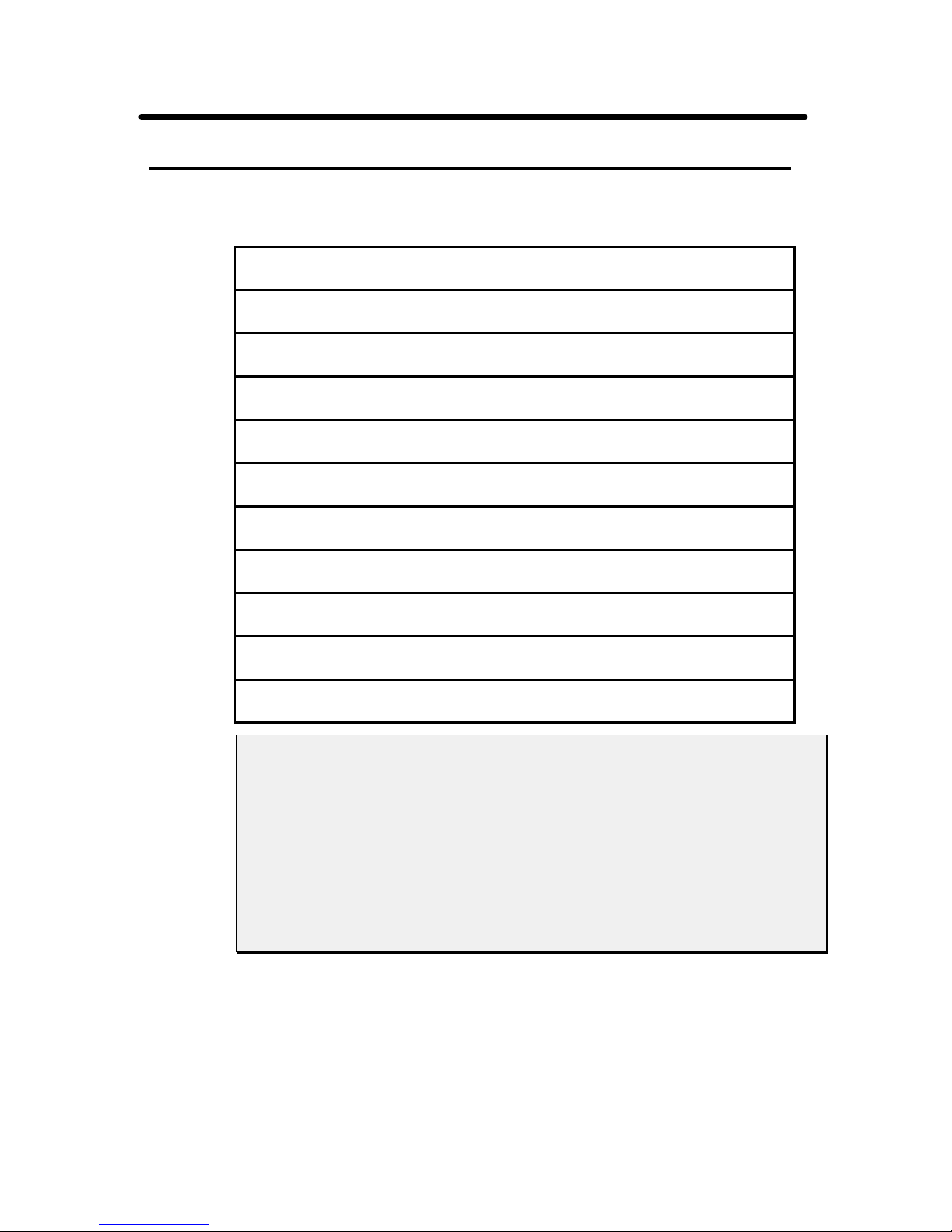
Peritek
SLOT
Figure 2-1 Example VMEbus Backplane
P1 P2
1 MVME167 (or equivalent) Single Board Computer
2 Peritek Graphics Board (VCT-V, VCU-V, or VCD-V)
3 Spare
4 Spare
5 Spare
6 Spare
7 Spare
^ Spare
|
Spare
v Spare
21 Spare
Note
Note: There must not be any open slots between the first and last boards
which use either DMA or interrupts (this includes the Peritek graphics
board, which uses interrupts).
The shorting jumper for Slot 2 IAKIN/OUT should be removed (assuming
the graphics board is installed in that slot). Shorting jumpers should be
installed for all unused slots..
2-6 Installing Your Peritek Graphics Board
Page 38

Peritek
3. Remove the interrupt pass/grant from the board slot.
The jumper may be on the front or back of the backplane. Some
backplanes don't have jumpers to remove. The jumper is an integral
part of the slot. It is activated automatically when the card is inserted.
4. Wear a grounded wrist strap. Touch a metal part of the computer
chassis, remove the graphics board from its anti static bag, and
immediately slide it into the slot.
Caution
The static electricity that your body builds up normally can seriously
damage the integrated circuits on the graphics board. You should first
touch the metal part of the chassis, which will short circuit the static
charge on your body to ground. It is preferable to wear a grounded wrist
strap whenever handling computer boards.
Handle the graphics board only by its edges. Oils from your hand can
break down the metal used in the circuit board.
5. After making sure the board is seated correctly, tighten the screwlock
on each end of the board.
6. Close the computer and plug the video cable into the monitor and the
graphics board. Make sure to plug the three BNC cables, colored red,
green, and blue, into the monitor's corresponding red, green, and blue
inputs. Also, make sure the 75 ohm switch on the monitor is turned on.
VGA monitors which use a 5-wire cable (which can be obtained on
special order), may also require modified initialization tables.
2.3.4 What's Next?
Now at this point you can continue to the next section, 2.3.5 Connecting
the Mouse, Keyboard, and Console, or if you are not using them, skip it
and go on to the following section, 2.3.6 Checking your Display.
Installing Your Peritek Graphics Board 2-7
Page 39
Peritek
2.3.5 Connecting the Mouse, Keyboard, and Console
This section applies only to applications which use a mouse (or trackball)
and keyboard. Plug in the mouse and the keyboard cables.
Note
If you have an older style Peritek board, it will have a 20-pin header which
accepts a ribbon connector instead of separate keyboard, mouse and
terminal connectors.
If your graphics board does not use PTERM, your ribbon cable will have
two connectors, labeled M and K. These letters stand for "mouse" and
"keyboard." Plug these connectors in to the mouse and keyboard.
If your graphics board uses PTERM, your ribbon cable will have four
connectors, labeled M, K, C, and S. These letters stand for "mouse,"
"keyboard," "console," and "special." The S plug is not used. Plug the
other three connectors in to the mouse, keyboard, and the console ports on
your computer.
Plug the mouse cable into the 9-pin male connector labelled MOUSE.
Plug an LK201 or LK401 keyboard into the RJ-11 socket labelled
LK401, or plug a PC keyboard with a PS/2 style connector or adapter
into the round 6-pin socket labelled PC KBD.
If you are using the PTERM terminal emulator, plug the console cable
from the computer into the 9-pin female connector labelled
CONSOLE.
PTERM supports 9600 baud. Jumpers control the data bits, parity, and
RTS/CTS and XON/XOFF protocol. See Section 2.4.10.
The console port of your computer should be set to these values. If you
have trouble matching the board and computer console ports, refer to
Chapter 6 or contact Peritek.
2-8 Installing Your Peritek Graphics Board
Page 40

Peritek
2.3.6 Checking your Display
Turn on the power and check your monitor's display.
If your graphics board does not use a PTERM terminal emulator or the
CnP Graphics Subroutine Package autoboot PROM there will be no
display. This is because the board doesn't have an automatic bootup
sequence to initialize itself.
Only when you boot your computer and the graphics board software
has been downloaded will you see anything. In the case of PX
Windows, your monitor should display a uniform stippled raster and a
colored cross cursor, which is controlled by the mouse. For the CnP,
you have to load both the CnP.RAM and a test program (e.g.
TQT01.RAM) before you will see anything.
If your graphics board uses the PTERM terminal emulator, a white,
rectangular cursor should appear in the upper left corner of the
monitor. As the computer boots, it should print messages on the
screen. If none appear, make sure the console connector is correctly
plugged in and the console terminal parity and data bits are set
correctly (see Jumper Settings).
Once you have a picture on the screen, you may need to adjust the
width, height, brightness, contrast, and hold controls on your monitor
to get a good, centered image. If these controls don't adjust the image
properly, the parameters used to set the 34020 graphics timing registers
might be wrong. If you encounter display problems with PTERM, the
timing parameters may need to be changed. However, are not user
definable; they are hard-coded into the PROM. Contact Peritek for a
different PROM set to set the correct display timings for your
installation.
If you encounter display problems when the X server or CnP is
running, the values in the initialization table you used may not be
correct (see the Section 5.4. You can select a different table or call
Peritek for assistance.
If you have any trouble with any part of the installation, refer to Chapter 6.
Otherwise, proceed to the instructions supplied in your software manual.
Installing Your Peritek Graphics Board 2-9
Page 41

Peritek
Figure 2-2 Jumper Locations for the VCT-V and VCU-V
2-10 Installing Your Peritek Graphics Board
Page 42

Peritek
Figure 2-3 Jumper Locations for the VCD-V
Installing Your Peritek Graphics Board 2-11
Page 43

Peritek
2.4 Option Selection
It is best to first test out a board with the factory default configuration
whenever possible. This minimizes the chance of introducing a problem
into a known good board when you are not very familiar with the product.
Sometimes, however, something must be changed. That is what this
section is for. Before changing addresses, please read the commentary on
VMEbus addressing which is in Section 6.2 of this manual.
The VCD-V, VCT-V, and VCU-V share virtually all jumper
configurations. Only the jumper locations differ. Therefore, this section
covers the changes to all three products. The VCT-V and VCU-V actually
use the identical PC board. They differ only with plug in parts such as
FPGA, color map, cursor, and memory configuration.
The following instructions tell how to modify the VCD-V FAB REV 2
(and on) and the VCU-V and VCT-V FAB REV 4 (and on) to a nonstandard configuration. Refer to Figure 2-3 Jumper Option Locations for
VCD and VCT/VCU (previous two pages) for jumper locations. For wirewrap changes, only KYNAR or TEFLON, not enamel or plastic coated,
insulated wire should be used.
2.4.1 CSR Addresses
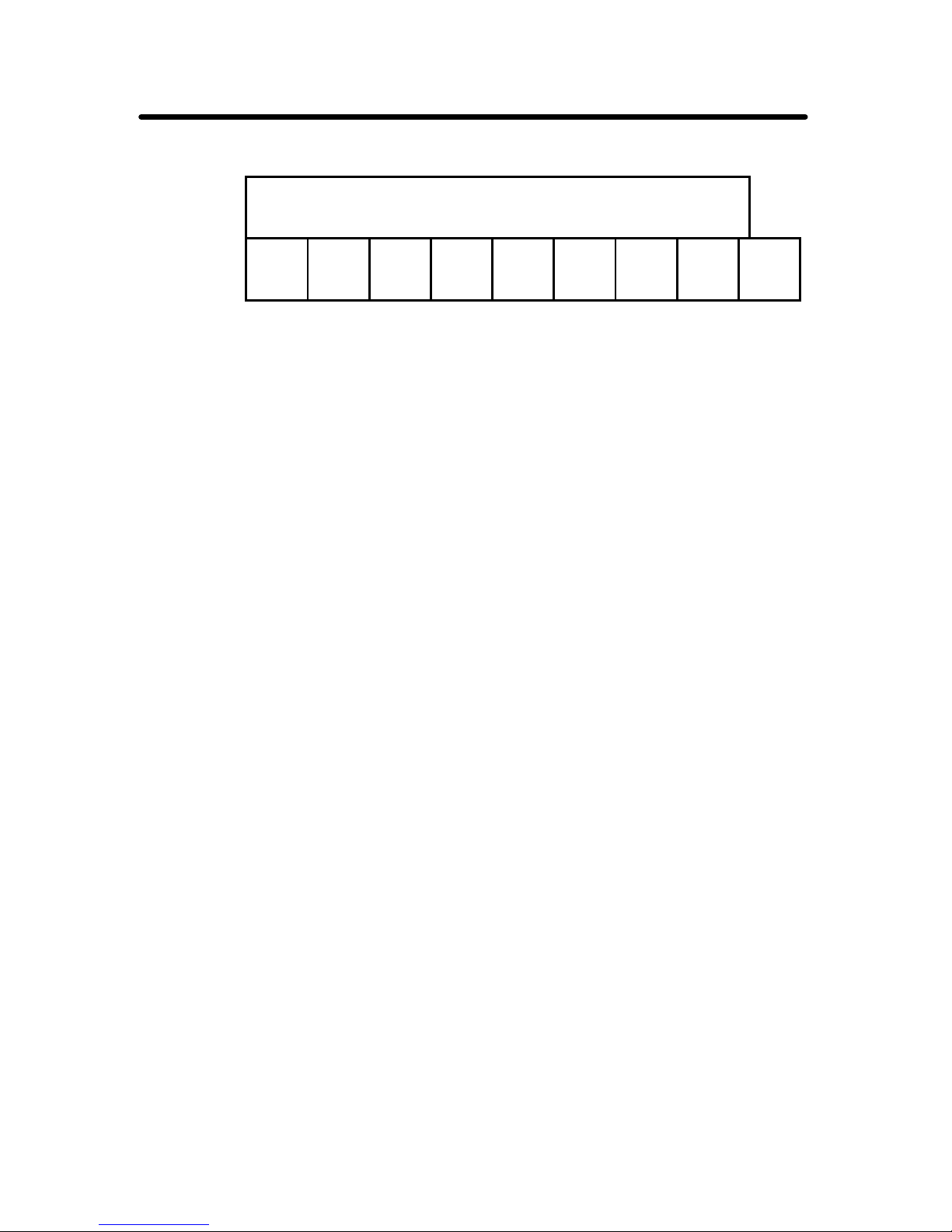
The address range for the CSR block is jumper selectable to certain
addresses in A16 space. As configured at the factory, bits 4, 5, 14, 15 are
used in the address selection, bits 0-3 are used in the register selection, and
bits 6-13 are hardwired low. If required, bits 6-13 can be some other
pattern - contact Peritek if you need this.
Remember that the base addresses for the Line Buffer, Extended Address
Block, and Interrupt Vector are all software programmable. Furthermore,
if you select the Alternate group 12-15, you will conflict with the standard
Line Buffer address (FFFF0000-FFFF03FF) used by Peritek software for
the Line Buffer. Section 5.2 has complete information about programming
these registers. Refer also to Chapter 6 and note the comments concerning
use of the Motorola MVME167 and MVME187.
2-12 Installing Your Peritek Graphics Board
Page 44
Peritek
Figure 2-4 CSR Address and Interrupt Grant Level Jumpers
8-pin resistor pack
1 2 3 4 5 6 7 8 9
Pin Number Function
1 GRD
2 A15
3 A14
4 A5
5 A4
6 VS2
7 VS1
8 VS0
9 GRD
Address Selection VMEbus (Hex) default jumpers
Standard xxxxC000-xxxxC00F A4, A5 installed
Alternate 1 xxxxC010-xxxxC01F A5 installed
Alternate 2 xxxxC020-xxxxC02F A4 installed
Alternate 3 xxxxC030-xxxxC03F --
Alternate 4-7 xxxx80n0-xxxx80nF A14, A5, A4
Alternate 8-11 xxxx40n0-xxxx40nF A15, A5, A4
Alternate 12-15 xxxx00n0-xxxx00nF A14, A15, A5, A4
Note: xxxx depends on host processor's A16 VMEbus address space.
2.4.2 Interrupt Grant Receive/Acknowledge
The VMEbus has a seven level interrupt grant receive/acknowledge
protocol which requires each board to acknowledge that it is responding to
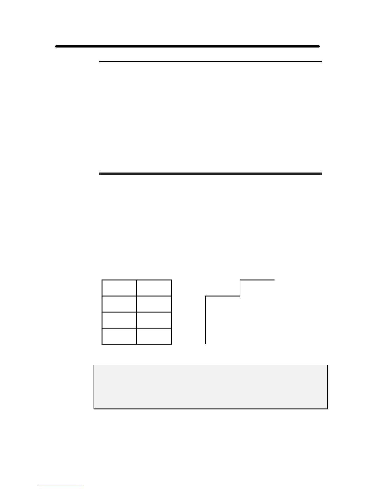
the interrupt grant level that it requested. Three jumpers set this response
level. Refer to the Jumper Location Figures for VCD and VCT/VCU and
Figure 2-4 (above) for the location of the jumpers. In the table below, 0
equals jumper installed.
Installing Your Peritek Graphics Board 2-13
Page 45
Peritek
Table 2-3 Interrupt Grant Level
Grant Level VS Jumper Number Default
1 0 0 1
2 0 1 0
3 0 1 1 yes
4 1 0 0
5 1 0 1
6 1 1 0
7 1 1 1
2.4.3 Interrupt Priority
2 1 0
The VMEbus interrupt request priority is jumper programmable for the
seven levels (1-7). The lower the priority number the less likely the board
will be serviced. The Interrupt Request Priority jumper is located to the
left side of J1 (VME P1 connector) and is labeled JP1. The pin layout is as
follows:
Figure 2-5 Interrupt Priority Jumpers
IRQ7 IRQ3
IRQ6 IRQ2
IRQ5 IRQ1
J1
IRQ4 IRQ
Caution
The Vector Priority setting must match the Interrupt Request Priority
setting.
2-14 Installing Your Peritek Graphics Board
Page 46

Peritek
2.4.4 Flash EEPROM
The graphics boards allocate address space for 32-bit wide EEPROM.
There are sockets for four 8-bit 32-pin PLCC Flash EEPROMS. Sizes
supported are 32Kx8 e.g. AM28F256-150JC (for 128 KB total) through
256Kx8 e.g. AM28F020-150JC (for 1 MB total). 1 wait state is provided
so access time should be less than 200nS. By virtue of the pin and address
arrangement on these devices no size jumpers are required.
Peritek has a program which is available upon request which can be used
to load images into the the EEPROMs. In order to allow the devices to
program, a jumper must be installed on the board to enable 12 Volts to the
EEPROMs (see below). If you have any questions, please contact Peritek.
VCD-V Program Voltage Enable
As shown in Figure 2-2, install a jumper between pins 2 and 3 of JP6.
VCT-V and VCU-V Program Voltage Enable
As shown in Figure 2-3, install a jumper between pins 2 and 3 of JP6.
Caution
Remove the jumper once you are done programming.
2.4.5 Autoboot Enable
The graphics boards can run automatically from on-board EEPROM on
powerup or anytime SYSRESET is asserted. Peritek can supply a terminal
emulator (PTERM) preloaded and ready to run (see Chapter 3). Note: if
this jumper is installed then autoboot EEPROMS must be installed,
otherwise the 34020 executes garbage.
VCD Autoboot Enable
As shown in Figure 2-2 and Figure 2-6 (below), install a jumper in the
jumper pair labelled BEN to enable autoboot operation.
VCT-V and VCU-V Autoboot Enable
As shown in Figure 2-3, the jumper pair just to the right of U27
(MACH230 chip near the center of the board) and is labeled JP18. Install a
jumper to enable autoboot operation.
Installing Your Peritek Graphics Board 2-15
Page 47
Peritek
2.4.6 DRAM and VRAM Size
The on-board 34020 DRAM and display memory VRAM are contained in
SIMMs (Single Inline Memory Module) and may be changed in the field.
Two pairs of jumpers allow for different size memories. The video
memory size is in pages, where one page = 1024 x 1024 pixels.
On the VCD-V, the jumpers are part of jumper strip JP5.
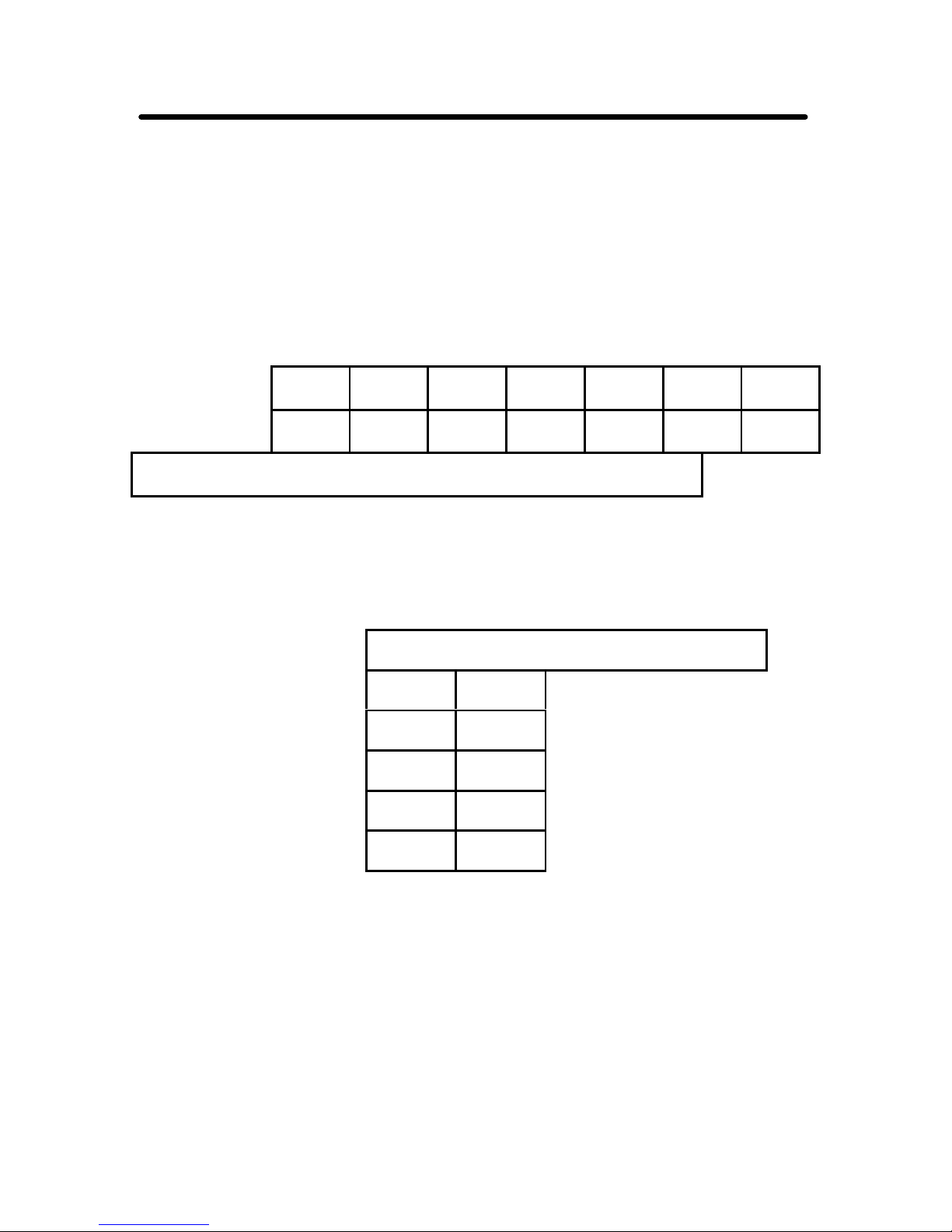
Figure 2-6 VCD-V DRAM and VRAM Size and Autoboot Enable
GRD GRD GRD GRD GRD GRD GRD
D0 D1 V0 V1 resv resv BEN
RP4
On the VCT-V and VCU-V, the jumpers are part of jumper strip JP19:
Figure 2-7 VCT/VCU DRAM and VRAM Size
Lower edge of U27 - MACH230
GRD D1
GRD D0
GRD V1
GRD V0
GRD resv
The tables on the next page shows how to set the DRAM and VRAM
jumpers. Note that for both the DRAM and VRAM tables, 0 = Jumper
Installed
2-16 Installing Your Peritek Graphics Board
Page 48

Peritek
Table 2-4 DRAM Size Jumpers
D1 D0 DRAM Size
0 0 1 or 4 MB
0 1 8 MB
1 0 16 MB
1 1 32 MB
Table 2-5 VRAM Size Jumpers
V1 V0 VCD-V & VCT-V
VCU-V VRAM Size
VRAM Size
0 0 1 page 2 page
0 1 2 pages 4 pages
1 0 4 pages 8 pages
1 1 4 pages 8 pages
2.4.7 Master Pixel Clock Oscillator Frequency
VCU-V and VCT-V
VCU-V and VCT-V boards have a software programmable pixel clock,
which allows virtually any frequency pixel clock to be chosen. Peritek
distributes an number of standard initialization tables, and can provide
custom versions upon request. See Section 5.4 for more information
The VCU-V uses the ICS1562 clock chip, which actually gives a
maximum pixel clock in excess of 200 MHz. Note that the BT468 color
map chip must be upgraded from its standard 170 MHz to take advantage
of this.
The VCT-V uses either the ICS1562 or the ICS1572 (in some special
configurations). The ICS1572 has a 150 MHz maximum clock frequency,
which is more than what the BT463 color map chip is limited to (135
MHz). The 1562 and 1572 take exactly the same program parameters.
Installing Your Peritek Graphics Board 2-17
Page 49

Peritek
VCD-V
Most VCD-V boards have a fixed frequency crystal controlled oscillator
to maintain compatibility with earlier revision VCD-Vs. However, a
software programmable pixel clock (ICS1572) is being phased into the
standard configuration VCD-V/X6/D8 and VCD-V/X12/D8 for new
customers only. If this presents a problem, please contact the factory.
Routines provided in Peritek's Graphics Subroutine Package and PX
Windows software are used to set the pixel clock. Please contact Peritek if
you require assistance in selecting a correct table from those distributed
with the software.
2.4.8 Interlaced Operation and VCU-V Slow Mode
Peritek's VCT-V and VCD-V/X6 type boards support interlaced operation
when the proper initialization is specified. No other changes are required.
The VCU-V and VCD-V/X12 type boards will operate in interlaced mode,
but the cursor appearance and positioning will not be correct. This is
because the cursor built into the color map does not know about interlaced
operation.
In order to run the VCU-V in 640x480 interlaced mode (or any mode with
a pixel clock of less than 18.25 MHz) the blanking jumper must be
changed to the slow mode. This jumper is labeled JP7 and is located just
below the BT468 (VCU-V) - see Figure 2.3. Connect pins 1 and 2
(leftmost 2 pins) for regular mode or connect pins 2 and 3 (rightmost 2
pins) for slow mode. The jumper may be left in the slow position for
resolutions up to 1280x1024, but the horizontal cursor position will be off
8 or 16 pixels. The minimum pixel frequency in the slow mode is 4 MHz.
2.4.9 BT482 Output Level (VCD-V/T - special order only)
A 15-turn potentiometer (R74) can be used to precisely adjust the peak
voltage level. Refer to Figure 2.2 for the location of the control, which can
be accessed through a small hole in the front panel near the VGA
connector.
2-18 Installing Your Peritek Graphics Board
Page 50
Peritek
2.4.10 Selecting PTERM Options
Table 2-6 PTERM Serial Control Options
Jumper Open Shorted
A 8 bits/No parity 7 bits/Even parity
B XON/XOFF disabled XON/XOFF enabled
C RTS/CTS disabled RTS/CTS enabled
The default with no jumpers installed is 9600, 8 bits, no parity, and no
flow control. The PC Keyboard is auto detected. If it is installed it will be
used, otherwise the LK401 serial interface will be used.
The XON/XOFF flow control only applies to data being sent to PTERM.
Keyboard data send from PTERM to the host is not flow controlled with
XON/XOFF.
PTERM has a 8KB input buffer so that it can handle bursts of up to 8KB
without requiring XON/XOFF flow control.
The RTS/CTS flow control is done by programming the UART to enable
UART control of the RTS/CTS lines. THIS OPTION HAS NOT BEEN
COMPLETELY TESTED. It is unlikely that the CTS signal will be
asserted because the 34020 should in general service UART interrupts
prior to the next character being received. The RTS signal will control
output from PTERM to the host. If this signal is not connected the UART
will refrain from sending characters to the host.
Figure 2-8 VCD-V PTERM Serial Jumpers (JP33)
RP20
RP23
GRD GRD GRD
A B C
RP15
Installing Your Peritek Graphics Board 2-19
Page 51
Peritek
Figure 2-9 VCT-V and VCU-V PTERM Serial Jumpers (JP22)
GRD GRD GRD
A B C
RP17
2.4.11 Selecting Serial I/O Options
Section 2.5.1 has connector pinouts for the Serial I/O ports. In the
follwoing tables, CnP Port refers to the way the Graphics Subroutine
Package uses these ports.
RP22
RP5
Note
Total current draw for all fused +5 volt outputs should not exceed .5 A.
Total current draw for all fused +12 volt outputs should not exceed .5 A.
There is a 470 ohm current limiting resistor in the -12 volt line. There is a
1K ohm current limiting resistor power source to the Mouse Connector
pins 4 and 7.
Table 2-7 Mouse Port or
CnP Port 0 (DUART 0 channel A)
Jumper Mouse Connector Pin Option Default
JP8 1-2 pin 3 to -12V yes
JP8 2-3 pin 3 to Port 0 TX no
JP20 1-2 pin 6 to Port 1 RX no
JP21 1-2 pin 8 to Port 1 RX no
JP10 1-2 (only) pin 9 to fused (.5A) +12 volts no
JP20 2-3 (only) pin 9 to fused (.5A) +5 volts no
The mouse port is a DB9 male connector.
Combined current draw on pins 4 and 7 should not exceed 10 mA. Current
draw on pin 3 should not exceed 10 mA.
2-20 Installing Your Peritek Graphics Board
Page 52

Peritek
Table 2-8 LK401 Keyboard Port or
CnP Port 1 (DUART 0 channel B)
There are no jumper options.
RJ11 "handset" type jack. Keyboard plugs straight in. Pin 2 is on the fused
(.5A) +12 volt supply.
Table 2-9 Console Port or
CnP Port 2 (DUART 1 channel A)
Jumper Console Port Connector Pin Option Default
JP13 1-2 pin 7 to CTS yes
JP13 2-3 pin 7 to Port 3 RX no
JP12 1-2 pin 8 to RTS yes
JP12 1-3 pin 8 to Port 3 TX no
JP11 1-2 (only) pin 9 to fused (.5A) +12 volts no
JP11 2-3 (only) pin 9 to fused (.5A) +5 volts no
The console port is a DB9 female connector.
At the connector, CTS is an input and RTS is an output. Not all
installations require these signals.
Table 2-10 Extra Port or
CnP Port 3 (DUART 1 channel B)
No connector is supplied for this port, but the signals can be output from
the Console Port with option jumpering. See Console Port Options, above.
Installing Your Peritek Graphics Board 2-21
Page 53

Peritek
2.5 Connections to the VCU-V, VCT-V, and VCD-V
With the introduction of the VCU-V and VCT-V FAB REV 4 and the
VCD-V FAB REV 2, the connector layout has been completely revamped
in the interest of providing a more "user friendly" front panel. The mouse
and keyboard connectors now use standard interface connectors and the
SCSI (available only by special order) has been moved to the VMEbus P2
standard SCSI pinout. A new option, the High Speed Port (HSP), also
makes use of the P2 A and C rows and cannot coexist with the SCSI
option. Only the Video connector and the VCD-V digital connector remain
un
changed from earlier revisions.
The 34020 emulator connector, while still included in the PCB artwork,
has been deleted as an orderable option. It is for factory use only. Contact
Peritek if you need emulator connections.
There are five unique connectors installed on the VCU-V, VCT-V, and
VCD-V. An additional 26 pin header is installed on the VCD-V for digital
output.
The connectors include:
Section 2.5.1a a console (PTERM) 9-pin female connector
Section 2.5.1b a Serial PC Mouse/Trackball DB-9 male connector
Section 2.5.1c a PS/2 mini-DIN PC Keyboard connector
Section 2.5.1c an LK401 (RS-232 serial) RJ-11 modular connector
Section 2.5.2 a VGA-style high density DB-9 video connector
Section 2.5.3 VMEbus P2 connections for High Speed Port (HSP)
Section 2.5.4 VMEbus P2 connections for SCSI port (VCT and VCU)
Section 2.5.5 Digital Video connector (VCD-V only)
2-22 Installing Your Peritek Graphics Board
Page 54

Peritek
2.5.1 Console, Mouse, Trackball, and Keyboard Connectors
The graphics board connectors match the standard connectors for the
Console, Keyboard, Mouse, and Trackball. Connectors are provided for
both LK401 (RS-232 type) keyboard and PC compatible keyboard. Note
that the graphics boards supports Data-Leads-Only RS232C for the
keyboard, but RTS/CTS is supported for the console terminal port. The
RTS/CTS lines can be redefined as an additional Data-Leads-Only
RS232C data port. Data-Leads-Only means that the XON/XOFF software
protocol must be used to control data flow.
Note
Section 2.4.11 provides information on the jumper configuration options
for the RS-232 ports.
Fused +12 and +5 are provided since the mouse and keyboard require
power. The +5 and +12 are protected by auto-resetting fuses, which are
actually PTC elements which reset automatically when an overload is
removed.
The Peritek Graphics Subroutine Package (CnP) includes general purpose
serial I/O routines, but has no knowledge of the device connected to the
port. Sample programs exist which process keyboard and mouse inputs,
but no "intelligent" keyboard or mouse software is available. That is why
we have PX Windows!
Peritek can supply cables and devices - please contact the factory for
ordering information.
2.5.1a Console
The console port is used in conjunction with the PTERM terminal
emulator, and allows the graphics board to function as a "dumb terminal".
The console port is connected to the host CPU serial terminal connector
(serial port 1 on most systems). The graphics board functions as a terminal
on power up. Once the PX Windows or Graphics Subroutine Package
program starts up the console terminal function goes away and may not be
recalled. No "hot-key" provision to dynamically switch between the
application program and PTERM exists at this time. However, in PX
Windows, the PTERM may be restarted by running a special program
which kills the server and starts up PTERM.
Installing Your Peritek Graphics Board 2-23
Page 55

Peritek
The console port is suitable for applications which require long cables,
because it uses the RS-232C electrical protocol which can support cable
lengths well in excess of 100 feet. Peritek uses a DB9 female D-Sub
connector.
Table 2-11 Console Connector Pinout
9-pin D-Sub Pin Number Description
1 not used
2 Transmit Data to Console Port
3 Receive Data from Console Port
4 not used
5 Ground
6 not used
7 CTS (from Console Port)
8 RTS (to Console Port)
9 not used
2.5.1b Mouse and Trackball
If you buy the Keyboard and Mouse or Trackball directly from Peritek they
will come tested and prepared to work correctly with Peritek PX Windows
and PTERM Terminal Emulator. The software will work automagically
with either a PC compatible keyboard or an LK401 compatible keyboard.
If no keyboard is installed the default is the LK401. The PX Windows
mouse or trackball should be a 3 button, Mouse Systems protocol (5 byte)
device, although the 2-button Microsoft Mouse protocol is now supported.
The Peritek Optical Mouse is a Mouse Systems Serial PC Mouse. It uses
optical technology for postioning, thus requiring a small pad, which is
included. Peritek can also supply the low-cost Peritek Roller Mouse
which uses a small rolling ball and mechanical position encoders. A pad is
not supplied, but can sometimes make the roller mouse operation
smoother. The Peritek Trackball works like an upside-down roller mouse,
but the ball is much larger.
In all cases, the unit operate in 3 button Mouse Systems protocol, which is
best suited for PX Windows. However, 2 button Microsoft Mouse mode
can be supported with a special command line option when starting the PX
Windows server (see the PX Windows User Manual "Man Page" section.
If you purchase your own mouse, make sure it can operate in the more
desirable 3 button mode.
2-24 Installing Your Peritek Graphics Board
Page 56
Peritek
The mouse relies on the current which can be sourced through the serial
port's transmit, RTS and CTS lines for power. However, since the graphics
board mouse port is really just data leads only, fused +12 and -12 volts are
supplied to these lines instead.
Both Peritek Mouse units are suitable for applications which require long
cables, because they use the RS-232C electrical protocol which can
support cable lengths well in excess of 100 feet. Peritek uses a DB9 male
D-Sub connector to pass data and power to the mouse, which requires +12
and -12.
Note
If you experience difficulty getting a device to work, especially a Mouse or
Trackball, you may be drawing too much current from pins 3, 4, or 7.
There are current limiting resistors in series with the power sources for
these lines.
Table 2-12 Mouse Connector Pinout
9-pin D-Sub Pin Number Description
1 not used
2 Data from Mouse
3 -12 Volts via 470 ohm resistor
4 +12 Volts via 1000 ohm resistor
5 Ground
6 not used
7 +12 Volts via 1000 ohm resistor
8 not used
9 not used
The resistors are to make the marginal RS-232 circuits of low-cost mice
and trackballs work correctly. They also limit current inrush which can
damage some devices.
Installing Your Peritek Graphics Board 2-25
Page 57

Peritek
2.5.1c Serial and PC Keyboards
Peritek Serial Keyboard
The Peritek Serial Keyboard is a DEC LK401-AA unit which is
especially suited for applications which require long cables. The Serial
Keyboard uses the RS-232C protocol which can support cable lengths in
excess of 100 feet. It is a 4800 baud unit, and supplies a keyswitch matrix
code to the software. It uses an RJ11 4 pin (handset) phone connector to
pass data and power (+12) to the Keyboard.
Table 2-13 LK401 Connector Pinout
RJ11 Pin Number Description
1 Data from Serial Keyboard
2 Fused +12 Volts
3 Ground
4 Data to Serial Keyboard
Peritek PC Keyboard
The Peritek PC Keyboard is suitable for applications which do not
require long cables, because it uses a TTL level electrical protocol which
cannot support cable lengths in excess of about 10 feet. 3rd party cable
extender/amplifiers are available to overcome this limitation. Peritek uses
the mini-DIN PS/2 keyboard connector to pass data and power (+5) to the
Keyboard. If you use a standard PC keyboard, you will need a PC DIN to
PS/2 mini-DIN adapter which is available from most computer stores.
Table 2-14 PC Keyboard Connector Pinout
PS/2 Mini-DIN Pin Number Description
1 Bidirectional Keyboard Data
2 not used
3 Ground
4 Fused +5 Volts
5 Bidirectional Keyboard Clock
6 not used
2-26 Installing Your Peritek Graphics Board
Page 58

Peritek
2.5.2 Video Connector
The video connector is a VGA style compressed 15 pin D-SUB. The R, G,
and B video outputs are driven by the RAMDAC, which is capable of
driving terminated cable (75 ohms) to standard RS-330/IRE levels. Cable
length should be limited to 50 feet unless you use low loss RG-59.
A VGA monitor can be plugged in directly, using a standard VGA
connector. You must use the correct initialization table, since a VGA
monitor depends on the sync polarities to determine operating frequency.
If you use the Peritek VGA-3/20 VGA to BNC cable, only composite
signals are carried to the monitor, and it will "autoscan", if the monitor is
so equipped.
The direction of the TTL Dot Clock, Vertical/Composite Sync, and
Horizontal Sync and the polarity of the Sync signals are controlled by a
combination of jumpers and the Zoom Control Register (see Section 5.5).
Table 2-15 Video Connector Pinout
Pin Description Pin Description
1 RED 8 GND
2 GREEN 9 GND
3 BLUE 10 GND
4 NC 11 HSYNCIN (for genlock option)
5 GND 12 VSYNCIN (for genlock option)
6 GND 13 HSYNCOUT
7 GND 14 VSYNCOUT or CSYNCOUT
Notes for External Sync
Genlock requires separate horizontal and vertical sync signals (active low)
to be input and a jumper change. HSYNCOUT (horizontal sync out)
polarity is programmable. CVSYNCOUT (composite or vertical sync out)
mode (composite or vertical) and polarity are programmable. Refer to
Section 5.5 for information on programming these pins. Contact Peritek if
you are interested in using this feature.
15 DOTCLOCKOUT on
VCD-V/A6 and X6
Installing Your Peritek Graphics Board 2-27
Page 59

Peritek
2.5.3 High Speed Data Port (HSP)
The output buffers on the User Equipment (UE) should be 74ACT374
(FCT, BCT, and ABT are OK), with 64 mA output drivers terminated with
220/330 resistors on the UE. Input signals (from the graphics board to the
UE) will be conditioned by a hysteresis device such as a 74F14. See
Section 5.15 for HSP signal functions.
Table 2-16 HSP P2 Connector Pin Connections
Signal Name Pin Polarity Direction UE Type Board Type
DATA_00 A1 active high VCD input 74ACT374 74ACT652
DATA_01 C1 active high VCD input 74ACT374 74ACT652
DATA_02 A2 active high VCD input 74ACT374 74ACT652
DATA_03 C2 active high VCD input 74ACT374 74ACT652
DATA_04 A3 active high VCD input 74ACT374 74ACT652
DATA_05 C3 active high VCD input 74ACT374 74ACT652
DATA_06 A4 active high VCD input 74ACT374 74ACT652
DATA_07 C4 active high VCD input 74ACT374 74ACT652
DATA_08 A5 active high VCD input 74ACT374 74ACT652
DATA_09 C5 active high VCD input 74ACT374 74ACT652
DATA_10 A6 active high VCD input 74ACT374 74ACT652
DATA_11 C6 active high VCD input 74ACT374 74ACT652
DATA_12 A7 active high VCD input 74ACT374 74ACT652
DATA_13 C7 active high VCD input 74ACT374 74ACT652
DATA_14 A8 active high VCD input 74ACT374 74ACT652
DATA_15 C8 active high VCD input 74ACT374 74ACT652
DATA_16 A9 active high VCD input 74ACT374 74ACT652
DATA_17 C9 active high VCD input 74ACT374 74ACT652
DATA_18 A10 active high VCD input 74ACT374 74ACT652
DATA_19 C10 active high VCD input 74ACT374 74ACT652
DATA_20 A11 active high VCD input 74ACT374 74ACT652
DATA_21 C11 active high VCD input 74ACT374 74ACT652
DATA_22 A12 active high VCD input 74ACT374 74ACT652
DATA_23 C12 active high VCD input 74ACT374 74ACT652
DATA_24 A13 active high VCD input 74ACT374 74ACT652
DATA_25 C13 active high VCD input 74ACT374 74ACT652
DATA_26 A14 active high VCD input 74ACT374 74ACT652
DATA_27 C14 active high VCD input 74ACT374 74ACT652
DATA_28 A15 active high VCD input 74ACT374 74ACT652
DATA_29 C15 active high VCD input 74ACT374 74ACT652
DATA_30 A16 active high VCD input 74ACT374 74ACT652
DATA_31 C16 active high VCD input 74ACT374 74ACT652
REL C25 active low VCD output 74F14/LS244 74ACT244
HSL C28 active low VCD output 74F14/LS244 74ACT244
VSL C27 active low VCD output 74F14/LS244 74ACT244
PRDYL C26 active low VCD input 74LS244 74F14/LS244
GND A17, A25, A26, A27, C17, C18, C19, C20, C24, B2, B12, B22, B31
VCC B1, B13, B32
2-28 Installing Your Peritek Graphics Board
Page 60

Peritek
2.5.4 8-bit SCSI Port (VCT-V and VCU-V)
For its optional SCSI port, Peritek follows the "standard" 8-bit SCSI
pinout on the VMEbus P2 connector popularized by Motorola. P2 is a 96
pin header (3 rows x 32 pins), with the B, or center row reserved for use
by the VMEbus address and data buses. Rows A and C are user assignable.
The SCSI port shares some of the same pins with the HSP (see Section
2.5.3, above). Therfore, you can't have both options on the same board.
The following table lists the P2 pin assignments and the corresponding
cable connections for the SCSI option. Remember that only the SCSI or
the HSP can be used on a particular board.
Table 2-17 VCU-Vand VCT-V SCSI Connections to VMEbus P2
P2 connector Standard SCSI Connector
Pin Signal Name Pin Signal Name
A1 Data Bit 0, Low Active 2 Data Bit 0, Low Active
A2 Data Bit 1, Low Active 4 Data Bit 1, Low Active
A3 Data Bit 2, Low Active 6 Data Bit 2, Low Active
A4 Data Bit 3, Low Active 8 Data Bit 3, Low Active
A5 Data Bit 4, Low Active 10 Data Bit 4, Low Active
A6 Data Bit 5, Low Active 12 Data Bit 5, Low Active
A7 Data Bit 6, Low Active 14 Data Bit 6, Low Active
A8 Data Bit 7, Low Active 16 Data Bit 7, Low Active
A9 Data Bit Parity, Low Active 18 Data Bit Parity, Low Active
A10 Attention, Low Active 32 Attention, Low Active
Spare, Low Active 34 Spare, Low Active
A11 Busy, Low Active 36 Busy, Low Active
A12 Acknowledge, Low Active 38 Acknowledge, Low Active
A13 Reset, Low Active 40 Reset, Low Active
A14 Message, Low Active 42 Message, Low Active
A15 Select, Low Active 44 Select, Low Active
A16 Command, Low Active 46 Command, Low Active
A17 Request, Low Active 48 Request, Low Active
A18 Input, Low Active 50 Input, Low Active
20 Spare
22 Spare
24 Spare
26 Spare
28 Spare
30 Spare
1-49 ODD-numbered pins are Ground
Build the cable so that only the signal lines are connected. The grounds
can be connected just on the peripheral end.
Installing Your Peritek Graphics Board 2-29
Page 61

Peritek
2.5.5 Digital Video Connector (VCD-V only)
The digital video connector is configured at the factory to support a variety
of different requirements. Type 1 supports 1 pixel per clock time, up to 8
bits/pixel. Type 2 supports 2 pixels per clock, up to 4 bits/pixel.
Connection tables are shown on the next 2 pages.
The issue of whether the graphics board should source power to the panel
is somewhat controversial. This is because there is a wide variety of panels
available and some draw a considerable amount of power. Peritek
recommends that you evaluate the power requirements carefully. In
addition, some panels require controlled power sequencing. It has been
Peritek's experience that if the panel and the graphics board are powered
on and off simultaneously that additional sequence control is not required.
Nevertheless, some users feel more strongly. The VCD-V as it exists today
does not include sequenced power. An ECO procedure does exist and can
be supplied if necessary.
The next circuit revision (available 4/95) will include sequenced +5 and
+12 sources on the digital connector. It will also include a wider video
data output path (up to 24 bits).
With respect to the Type 1 panels, since the VCD-V has an 8 bit output
port, and the human eye is least sensitive to variations in blue, the three
bits of blue available on the color panels has been reduced to two bits by
connecting B0 (LSB) and B2 (MSB) together for PX Windows
applications. If you are not using PX Windows, you are free to connect the
lines up in any way you wish. The following table shows some sample
color values.
2-30 Installing Your Peritek Graphics Board
Page 62

Peritek
Table 2-18 PX Windows Basic Color Table for Type 1 TFT-LCD
Panels
RGB Input Values
Color R0 R1 R2 G0 G1 G2 B1 B0/B2
Black 0 0 0 0 0 0 0 0
Blue 0 0 0 0 0 0 1 1
Green 0 0 0 1 1 1 0 0
Light Blue 0 0 0 1 1 1 1 1
Red 1 1 1 0 0 0 0 0
Purple 1 1 1 0 0 0 1 1
Yellow 1 1 1 1 1 1 0 0
White 1 1 1 1 1 1 1 1
Red Scale 0 0 0 0 0 0 0 0
(darker) 1 0 0 0 0 0 0 0
. . . . . . . . .
(brightest) 1 1 1 0 0 0 0 0
Green Scale 0 0 0 0 0 0 0 0
(darker) 0 0 0 1 0 0 0 0
. . . . . . . . .
(brightest) 0 0 0 1 1 1 0 0
Blue Scale 0 0 0 0 0 0 0 0
(darker) 0 0 0 0 0 0 1 0
. 0 0 0 0 0 0 0 1
(brightest) 0 0 0 0 0 0 1 1
Installing Your Peritek Graphics Board 2-31
Page 63

Peritek
Table 2-19 J4 - Type 1 Digital Video Connector to Sharp TFT-LCD Panels
VCD-V J4 connector PX Windows LQ10D011 LQ10DH11 LQ10DH15 LQ10D021
Pin Signal Name Signal Name Pin Pin Pin Pin
1 Data bit 0 R0 3 4 4 CN1-5
3 Data bit 1 R1 4 3 3 CN1-6
5 Data bit 2 R2 5 6 6 CN1-7
7 Data bit 3 G0 7 8 8 CN1-9
9 Data bit 4 G1 8 7 7 CN1-10
11 Data bit 5 G2 9 10 10 CN1-11
13 Data bit 6 B1 12 11 11 CN1-14
15 Data bit 7 B0,B2 11,13 12,14 12,14 CN1-13,15
17 /Composite Blank n/a -- -- 22 CN2-5
19 /Horizontal Sync n/a 15 16 16 CN1-3
21 /Vertical Sync n/a 17 18 18 CN1-4
23 Pixel Clock n/a 1 2 2 CN1-1
25,26 +5 Volts -- use direct power supply connection --
2 Ground n/a 2 1 1 2
4 Ground n/a - 5 5 -
6 Ground n/a 6 - - -
8 Ground n/a - 9 9 8
10 Ground n/a 10 - - 12 Ground n/a - 13 13 12
14 Ground n/a 14 15 15 16 Ground n/a 16 - - -
18-24 Ground n/a - - - -
Computer power supply +5 18 17 17 CN2-1,2
+12 20 19 19 --
Ground 19 20 20 CN2-3,4
Lighting n/a Backlit Backlit Backlit Edgelit
Power Sequencing? n/a yes yes yes no
Typical power sequence: power-up: +5 on --> logic on --> +12
power-down:+12 off --> logic off --> +5 off
Panel Model Logic/Power Connector Power Connector(s)
LQ10D011 Hirose DF11-22DS-2C Molex 51005-0800 (backlight)
LQ10DH11 Hirose DF11-22DS-2C Molex 51005-0800 (backlight)
LQ10DH15 Hirose DF11-22DS-2C Molex 51005-0800 (backlight)
LQ10D021 Hirose DF13-15S-1.25C Hirose DF13-6S-1.25C (logic)
JST S2B-EH (backlight)
2-32 Installing Your Peritek Graphics Board
Page 64

Peritek
Table 2-20 J4 - Type 2 Digital Video Connector to Sharp EL Panels
Sharp EL Panel Model LJ64ZU48/9
J4 J4 connector Standard Sharp Sharp
Pin Signal Name Pin Name Pin Name Signal Name
1 Pixel 1, Data bit 0 24 B2 D10
3 Pixel 1, Data bit 1 23 A2 D11
5 Pixel 1, Data bit 2 22 B3 D12
7 Pixel 1, Data bit 3 21 A3 D13
9 Pixel 0, Data bit 0 20 B4 D00
11 Pixel 0, Data bit 1 19 A4 D01
13 Pixel 0, Data bit 2 18 B5 D02
15 Pixel 0, Data bit 3 17 A5 D03
17 no connect
19 /Horizontal Sync 11 A8 HSYNC*
21 /Vertical Sync 9 A9 VSYNC*
23 Pixel Clock/2 13 A7 2CLK
25,26 +5 Volts -- use direct power supply connection -2,4,6,8 Ground -- -- --
10 Ground 10 B9 GND
12 Ground 12 B8 GND
14 Ground 14 B7 GND
16,18,20,22,24 Ground -- -- --
Power Supply +5 volts 3,4 A12,B12 VL
+24 volts 5,6 A11,B11 VD
Ground 7,8 A10,B10 GND
Logic/power connector is a standard dual row standard .1" connector
Installing Your Peritek Graphics Board 2-33
Page 65

Chapter 3
Software Summary
3.1 Introduction
This chapter provides an overview of Peritek's software offerings. Peritek
also has Software Product Descriptions and complete Technical Manual
sets for the PX Windows and Graphics Subroutine Package products.
Peritek provides software for the VCU-V, VCT-V, and VCD-V including
Peritek PX Windows (X11R6 X Windows Server), 34020 Compiler Tools,
Peritek simple console Terminal emulator (PTERM), and a comprehensive
Graphics Subroutine Package (generically CnP). The following table
summarizes the current availability. Contact Peritek if your choice is not
shown.
Software Summary 3-1
Page 66

Peritek
3.2 Software Availability by Platform and OS
Table 3-1 Peritek Software and Operating Systems Support
Operating
System
Current OS
Version CPU Type PX Windows
Subroutine
Package
HPUX 9.0 PA/RISC yes no
LynxOS 2.2 68K yes no
OSF/1 3.1 Alpha yes no
OS9 3.0 68K yes yes
pSOSystem 2.0 68K yes yes
SGI 5 R3000 yes yes
Solaris 2.3 SPARC yes no
SunOS 4.1.3 SPARC yes yes
Unix/V68 SVR3 68K yes yes
Unix/V88 SVR4 88K yes yes
VMEexec 68K 3.0 68K yes no
VMEexec 88K 3.0 88K yes no
VxWorks 5.1 68K yes yes
VxWorks.alpha 5.1 Alpha yes no
VxWorks.sparc 5.1 SPARC yes no
In addition to being available on tape media, the board side of PX
Windows, PTERM, and CnP Subroutine Package can be provided in
PROM. Jumpers permit the board to "autoboot" into the terminal emulator
for use as a console terminal (see Section 3.4 below).
3-2 Software Summary
Page 67

Peritek
3.3 Write Posting
Features of many of the newer CPU designs include pipelining and write
posting. The CPU, which is much faster than the VMEbus interface, is
allowed to store (or post) a write operation to the CPU board's VMEbus
controller. The controller takes care of the write within the timing
requirements of the VMEbus. Pipelining is a procedure whereby the CPU
can process more than one instruction at a time. As a result, instructions
are not necessarily completed in the order that they were started.
In the case of sequential accesses to the VMEbus, which the Peritek baords
use, it can happen that the a write of the Peritek graphics board Line
Buffer can occur before a write to the Line Address Register (LAR) has
been completed. If you had wanted to change the LAR and then write, you
are not guaranteed that this has happened. This results in incorrect
operation. The way to get around this is to immediately read back the data
which has been written to the LAR, which flushes the pipeline and ensures
correct operation. Since this is a problem just for the LAR, the
performance impact is minor.
Peritek can supply its software with the read after write operation already
incorporated. When ordering software, be sure to specify the CPU. Known
offenders include 68040 and MIPS R3000 based CPUs.
Software Summary 3-3
Page 68

Peritek
3.4 PX Windows Server
Peritek's PX Windows Server is a Motif client compatible X Windows
X11R6 board based server for a variety of Operating Systems (see Table
3-1). All functions of the server are actually executed by the 34020, which
maximizes performance and eliminates many host processor
responsibilities.
Peritek supplies the hardware specific parts of the X Window System,
which is the server. Peritek has written its own highly optimized graphics
layer for the 34020. The software is broken up into 2 functional parts: the
board-based X server and the CPU host side "stub program" which
provides a communication link between the server, clients, and the CPU
network and file system resources.
The board side server code also provides complete support for PCcompatible keyboard or LK401-AA keyboard and Microsoft 2-button and
Mouse Systems 3-button compatible pointing devices (i.e. mouse or
trackball).
X Windows is a machine independent network based windowing system.
It divides graphics functions into two parts:
1) The server, which controls the hardware dependent functions such as
the mouse, keyboard or trackball, and graphics display; and
2) The client(s), which is (are) the actual programs which the user wants
to interact with. This might include a terminal emulator, desktop
publishing program, or an image processing package. The client
application is usually linked with the standard XLIB library which
manages the actual communications between clients and the server.
Most operating systems come supplied with a local xlib and a standard
client package. Many also come with the Motif window manager. Contact
your OS vendor for specifics on what they supply.
Under certain circumstances and for particular operating systems, Peritek
can supply an extended version of PX Windows which includes a client
side package (including Motif). As this software is currently in
development, please contact Peritek for availability.
3-4 Software Summary
Page 69

Peritek
3.5 Graphics Subroutine Package
The Graphics Subroutine Package, comprises a significant "value-added"
component for the Peritek graphics controllers. It is called CDP for VCDV, CUP for the VCU-V, and CTP for the VCT-V and is termed generically
here as CnP. It is intended for the user who wishes to interface an
application program directly to the board. The subroutine package is based
on the TI math/graphics library. Modified and enhanced by Peritek, this
package contains over 200 subroutines. This package is designed to allow
the user to program the board without having to contend with all the
hardware details.
The package is compatible with BSD and System V Unix and many realtime operating systems. Operating systems using memory management
must allow the user to map to the portions of the I/O page where the board
registers are accessed. The packages will map the I/O page for operating
systems using memory management.
The package is a library of subroutines which run under a shell on the
graphics board and provide functions for the board. All characters are
software defined patterns which are drawn in the graphics memory. The
subroutine package supplies a variety of bit-mapped fonts including
contemporary and typewriter styles in different weights and pitches. Two
versions of CnP are included:
a) A hybrid version wherein a front end process running in the host
computer interprets subroutine calls and directs commands to be
executed by the 34020 on the graphics board. In some cases it is more
efficient to directly execute these functions, so the 34020 is not used.
b) A board based version for standalone programs. The user links the CnP
with an application program developed with Peritek's Program
Development Package (compiler, assembler, and linker - see section
3.2). CnP and the application run entirely on the graphics board.
Other software shipped with CnP includes initialization, demo programs,
34020 downloader, and 34020 utilities. Most programs are supplied in
source and executable and are written in C.
A complete list of the Graphics Subroutine Package library functions is
available upon request from Peritek. A sampling of the functions is shown
on the following page.
Software Summary 3-5
Page 70

Peritek
Table 3-2 Graphics Subroutine Package Library Routines
Initialization Functions clear_screen, new_screen, init_grafix,
init_palet, init_screen, init_text,
init_video, init_vuport
3D Transformation Functions copy_matrix, copy_vertex, init_matrix,
perspec, rotate, scale, transform, translate,
vertex_to_point
Text Output Functions draw_char, draw_string
Text Attribute Functions add_text_space, char_high,
char_wide_max, get_ascent, get_descent,
get_first_ch, get_last_ch, get_leading,
get_width
Font Management Functions get_font_max, install_font, select_font
Graphics Output Functions bound_fill, bound_patnfill, draw_line,
draw_oval, draw_ovalarc, draw_point,
draw_polyline, draw_rect, fill_convex,
fill_oval, fill_piearc, fill_polygon,
fill_rect, frame_oval, frame_rect,
patnfill_oval, patnfill_polygon,
patnfill_rect, patnfill_convex,
patnfill_piearc, patnframe_oval,
patnframe_rect, patnpen_line,
patnpen_ovalarc, patnpen_piearc,
patnpen_point, patnpen_polyline,
pen_line, pen_ovalarc, pen_piearc,
pen_point, pen_polyline, styled_line,
seed_fill, seed_patnfill
Pixel Functions bit_expand, get_pixel, get_rect,
move_pixel, put_pixel, run_decode,
run_encode, zoom_rect
3-6 Software Summary
Page 71

Peritek
Table 3-2 Graphics Subroutine Package Library Routines (continued)
Graphics Attribute Functions gets_patn_max, gets_pmask, gets_ppop,
gets_psize, gets_transp, install_patn,
select_patn, set_color0, set_color1,
set_pensize, set_pmask, set_ppop,
transp_off, transp_on, cmmw_command,
cmmw_readmask
Color Palette Functions cmmr_command, cmmr_readmask,
hls_rgb, rgb_hls, rgbrd, rgbwrt, cmmrblk,
cmmwblk, hlsrd, hlswrt
Viewport Functions close_vuport, copy_vuport, cpw,
get_vuport_max, move_vuport,
open_vuport, select_vuport, set_cliprect,
set_origin, size_vuport
Miscellaneous Functions delay, lib_id, lmo, rmo, peek_breg,
poke_breg, rep_pixel, wait_scan, xytoaddr,
pan, panrl, zoom_vert, zoom_horiz
Double Precision Functions acos, asin, atan, atan2, ceil, cos, cosh,
cotan, exp, fabs, floor, fmod, frexp, ldexp,
log, log10, modf, pow, sin, sinh, sqrt, tan,
tanh
Array Conversion Functions fix_to_float, fix_to_long, fix_to_short,
float_to_fix, long_to_fix, short_to_fix
Serial I/O Routines sio_break, sio_error, sio_iflush, sio_init,
sio_oflush, sio_peek, sio_read, sio_write
Software Summary 3-7
Page 72

Peritek
3.6 PTERM Terminal Emulator
Peritek has written a terminal emulator for use as a simple interface where
a console terminal is not available. It is not a VT100 emulator and doesn't
support escape sequences - its functionality is at the level known as "dumb
terminal emulator". It is, nevertheless, very useful. PTERM can be
combined in PROM with PX Windows or CnP.
PTERM can be used to initiate an OS boot procedure. Once the OS is up,
PX Windows can be started, whereupon PTERM ceases to function.
Console terminal output can be redirected to an xterm window, By running
a special program, PX Windows can be killed and PTERM restarted.
There is, at this time, no hot-key function to permit dynamic switching.
A cable is connected between the host computer's console port and the
graphics board Console Port. In addition, a Peritek keyboard must be
connected to either the graphics board's LK401 or PC Keyboard port. The
program runs the console link at 9600 baud, selects automatically between
PC Keyboard or LK401 Keyboard and can be jumper configured for 7 or 8
bit data, and RTS/CTS or XON/XOFF (see Section 2.4.10).
3-8 Software Summary
Page 73
Peritek
3.7 Software Development Package
A SunOS-based C compiler, cross-assembler, and linker for user written
34020 applications is available from Peritek. Its general characteristics are
described below. Contact Peritek for availability.
Figure 3-1 Software Development Flow
C source files
|
C compiler
|
object files assembler
source
| |
archiver assembler
| |
object
libraries
COFF object
files
V V
graphics
subroutinel
---->
linker
ibrary
---->
LD, DMP, GO, HLT, OFF,
WT, and TIDTSK
Software Summary 3-9
Page 74

Peritek
Features of the 34020 Development Tools
* Standard Kernighan and Ritchie C Compiler with extensions - compiles
standard C programs as defined by The C Programming Languge. This is
a full-featured optimizing compiler, using advanced techniques for
generating efficient, compact assembly code. The compiler supports
these standard extensions: enumeration types, structure assignments,
passing structures to functions, and returning structures from functions.
* Assembly Language output is generated by the compiler from the C
source. An interlist utility associates each C source line with its
corresponding assembly code output. The Assembler translates the
assembly language source output from the compiler into 34020 machine
language object files. The Linker combines all object files into a single
executable module.
* The archiver allows you to collect a group of source or object modules
into a library. It also permits you to modify a library by deleting,
replacing, extracting, or adding members. It is functionally equivalent to
ar (Unix).
3-10 Software Summary
Page 75

Peritek
3.8 Ancillary Programs
Some basic utilities are included with the Graphics Subroutine Package
(CnP) which can be used to see that the board works. This section will tell
you a little about these programs, but for complete information, please
refer to Peritek's TMS34020 Software Manual.
Program Manual
Name Section Description
Initialization 3.8.1, 5.4 Initialization tables
Install 3.8.2 Software installation examples.
VCnVINT 3.8.3 Initialize the graphics board.
VCnVTST 3.8.4 Test memories and control registers.
VCnVLD 3.8.5 Load and execute a 34020 demo programs
VCnVWT 3.8.6 Wait for a task to complete.
VCnVHLT 3.8.7 Halt a 34020 program.
VCnVGO 3.8.8 Restart a 34020 program.
VCnVOFF 3.8.9 Turn of the MEMON bit.
VCnVDMP 3.8.10 Formatted dump of 34020 memory.
TIDTSK 3.8.11 Formatted dump of COFF data.
-- 5.4 34020 initialization table examples
3.8.1 Initialization Tables
Programs which initialize the graphics board are shipped in source and
executable form. Initialization parameters that are used within some
programs are provided as ASCII files. A list of tables is provided in
Section 5.4. Both PX Windows and CnP are distributed with a host of
tables appropriate for a wide variety of applications. Please contact Peritek
if you have difficulty selecting a table or getting a good display.
3.8.2 Software Installation Examples
Be sure to consult the printed release notes which accompany your
software before attempting to install or run any programs. Some of
the programs described here or elsewhere in this manual may not be
included in your distribution. Conversely, there may be programs included
on the tape which are not mentioned at all in this manual. Both the PX
Windows and Subroutine Package manuals have complete installation
procedures.
Software Summary 3-11
Page 76

Peritek
While the recovery procedures described below should be sufficient to
recover the files, please refer to the printed release notes which
accompanied the media. The Unix distribution is made in TAR format
tape. The following procedure is for installing the tape.
1) Insert tape
2) Create a directory on the disk where you want to install the tree.
3) Change the default directory to that directory
4) Activate TAR
5) when finished, type
3.8.3 VCnVINT
Purpose: To initialize CnP and clear all memories. When done, load a
simple task into system memory and start the 34020. It is recommended
that this program be included in the user's startup command file. If the
graphics board registers and memory are not found at the expected
addresses, VCnVINT gives an error message and exits.
tar x
mt offl
to rewind and unload the tape.
VCnVINT was designed to run before the Graphics Subroutine Package is
loaded into the board. VCnVINT has several command line options which
supports specification of a non-standard CSR address and line buffer
addresses. Refer to the sample scripts for the different OS's to see how to
use this program. A number of standard initialization tables are supported
and are supplied. See Section 5.4 for more information.
3.8.4 VCnVTST
Note: Contact Peritek for availability of this program. Supported only
on VxWorks.
Purpose: To test the control registers, interrupts, TMS34020 Graphics
System Processor chip (CnP), the primary and overlay graphics display
memory, 34020 system RAM, DUARTs, cursors, and color map chips.
Description: VCnVTST is a menu driven program which allows the user
to select any or all tests, and to change 34020 parameter registers
interactively.
Three menus are supported: The master menu, the 34020 register menu,
and the test menu. Since significant effort has been made to make
VCnVTST "user friendly", the features of the program are pretty self
3-12 Software Summary
Page 77

Peritek
explanatory. However, instructions are included in Peritek's TMS34020
Software Manual.
VCnVTST thoroughly tests the registers and RAM sections on the board.
Bad results in some tests will prevent other tests from being run. A bad
LAR, for instance, will prevent execution of the RAM diagnostics.
Tests are run on the control register block for read/write bits. The
read/write bits in each register are tested by writing and reading back an
incrementing pattern. If the pattern read back does not match what was
written, an error message is printed with the bad bits set in a binary word.
A register uniqueness test is run on the read/write registers within each onboard device. A unique pattern is written to each register, with an
immediate readback performed after each write to verify proper access.
After all of the registers have been written into, another readback is
performed to see that each register still has its unique pattern, thereby
verifying that the registers are being addressed correctly.
Two diagnostic tests are performed on each RAM and the color and cursor
maps. The first test, the RAM uniqueness test, tests RAM addressing by
verifying that each address references a unique location. In this test a
unique value is stored at each address in the memory region under test. As
each location is written into, an immediate readback is performed to rule
out RAM and data line failures. After every address in the memory region
under test has had a unique value written to it, readback of the whole
memory is performed. If a non-unique location is found (i.e., an addressed
location does not contain what was originally written to it) the last address
to access the location can be determined by the new data in the location.
The first and last addresses that referenced that location are printed in an
error message. Three passes are required for the GRAM and System RAM,
first testing byte addressing, then word addressing, and finally, line
addressing.
The second test, the RAM pattern test, makes several passes through the
memory using different data patterns in an effort to detect pattern-sensitive
failures. In each pass, a pattern is written to every word and then its
complement is written to every third word. When the whole memory is
filled, a readback check is made.
When an error occurs, the bad bits are OR'ed into a word (initially all
zero's) and AND'ed into another word (initially all ones). The 16-bit word
address is formed and is OR'ed and AND'ed in a similar manner. Testing
continues until the entire memory has been checked with the current
pattern. If any errors have been detected, this test is terminated (after
Software Summary 3-13
Page 78

Peritek
completing testing with the current pattern) and an error message is
displayed on the console device.
VCnVTST has command line options similar to VCnVINT. Please refer to
the Peritek TMS34020 Software Manual for a description.
3.8.5 VCnVLD
Description: VCnVLD is used to load premade 34020 tasks to be loaded
into the graphics board and executed. Numerous programs of the form
file.RAM are supplied. VCnVLD has the command line options which
allow you to specify the name of the task to be loaded and to force the
loader to wait (normally VCnVLD does not wait for the 34020 task to
complete before exiting). You also have the same non-standard CSR and
line buffer options available in VCnVINT.
3.8.6 VCnVWT
Purpose: Wait for a task started by VCnVLD to complete. This program
duplicates the second half of VCnVLD. If you didn't run VCnVLD with
the -wait option you can "wait" later by running this program.
3.8.7 VCnVHLT
Purpose: Halt a program running in the 34020. This program is used to
debug on board code. It flushes cache and halts the 34020.
3.8.8 VCnVGO
Purpose: Restart a program previously loaded and running in the 34020.
This program is used to debug on board code and can used in conjunction
with VCnVHLT. It restarts the 34020 at the point at which it was halted
(not at the beginning of the 34020 program).
3-14 Software Summary
Page 79

Peritek
3.8.9 VCnVOFF
Purpose: Clears the MEMON bit in the VCnV CSR register. Normally
this is not necessary, since all host programs clear this bit on termination.
However, if the program did not finish normally, it may be necessary to
run this program (especially if you have boards which share the same line
buffer addresses).
3.8.10 VCnVDMP
Purpose: Dumps formatted portions of board memory to the terminal.
This program is useful for dumping the 34020 register block or video
memory. Output is similar to the Unix od command. Command line
options allow on to specify address type and format and data size and
format.
3.8.11 TIDTSK
Purpose: Provides to the terminal a formatted dump of COFF 34020
download images.
Software Summary 3-15
Page 80

Chapter 4
Theory of Operation
4.1 Introduction
This chapter contains a somewhat detailed look at the proprietary parts of
the graphics board design. Standard devices, such as color map chips and
DUARTs are not covered here. Chapter 5 has some relevant information
about the devices. Otherwise, we depend on the manufacturer's data sheet
to provide complete information.
Section 1.2 contains a complete Functional Description. Please refer to
that section before continuing with this chapter.
This chapter has the following sections:
4.2 System Architecture
4.3 Master Clock
4.4 VMEbus Interface
4.5 VMEbus Interrupt Controller
4.6 System Arbitration
4.7 Display Memory
4.8 System Memory
4.9 Summary of Programmed Devices
Theory of Operation 4-1
Page 81

Peritek
4.2 System Architecture
As noted before, this manual deals with all three of Peritek's 34020-based
graphics boards. The awkward places which result are in having to
delineate differences between boards, while maintaining a coherent flow in
the material. In this chapter, the overall board architecture and feature set
is the same. The most significant differences arise out of the variety of
display output options: 24 bit true color for the VCT-V, 8 bit color for the
VCU-V and VCD-V, and digital output for the VCD-V. Referring to the
block diagram appended to this chapter, it is evident that the VCD-V,
VCT-V, and VCU-V graphics boards are divided into two main sections:
the VMEbus interface section and the TMS34020 section.
VMEbus Interface
Rather than use a commercial VMEbus interface controller such as the
VIC064 or the SCV64, Peritek uses a proprietary chip set which is tailored
to the interface requirements of the 34020. Implemented in 3 high density
AMD MACH FPGA devices, the chip set includes control signals for the
VMEbus bus drivers, address decoders for the VMEbus, Control/Status
Register (CSR), Line Address Register (LAR), Line Buffer Address
Register (DBRADR), Extended Address Register (XAR), Interrupt Vector
Address Register (IVAR), an interrupt controller, VMEbus/34020
arbitrator and a byte swapper (see Section 5.3).
Control Registers
The 4 word CSR/LAR group and a 1 KB line buffer are all in the A16
space. A control bit can be used to enable A24 operation for the line buffer
when the VMEbus host doesn't support A16/D32 transfers. D32 capability
is important because long word data transfers will go twice as fast.
The CSR provides basic control over the board, including 34020 reset, line
buffer response enable, A24 enable, A32 enable, hardware byte swapper
enable, and interrupt enable. The LAR selects which 1 KB section of
memory or block of device registers is accessed through the line buffer.
The line buffer mechanism is used instead of direct addressing because the
internal memory capacity of the graphics board is in excess of 48 MB,
which is a substantial amount of address space, one that is outside the
reach of both A16 and A24 bus masters. Alternatively, the graphics board
can respond to a 64 MB section of A32 VMEbus address space, which
might be convenient for a disk controller. Note that Peritek software
4-2 Theory of Operation
Page 82

Peritek
supports only the A16 and A24 space addressing modes except for multiprocessor arbitration on Sun and Motorola 188 systems.
The on-board interrupt controller supports an interrupt from the 34020 to
the VMEbus host. Interrupt level is jumper selectable.
34020/VMEbus Host Interface
The VMEbus/34020 arbitrator allows the VMEbus to access not only the
CSR group but also the 34020-side devices. The 34020 participates in the
termination of those cycles, since it must synchronize them to its own bus
activity. The latching bus transceivers are actually controlled by the 34020,
which reads or writes them in conjunction with the completion of the cycle
requested by the arbitrator.
34020 Functional Unit
The 34020 section of the graphics board is a unit unto itself. It includes
display and 34020 (system) memory, writemask register, color maps
(which one is installed depends on configuration), 2681 DUART (serial
I/O), 8242PC keyboard controller, and local memory and device decoding.
Really, the two sections have little to do with one another except for
passing data back and forth - once loaded with a program and started, the
34020 can run independently of the VMEbus host. Except for the CSR
group, the 34020 has complete control over the functions of the board. The
VMEbus, going through the 34020 "host interface", also has ready access
to those functions. The 34020 provides a very fast and efficient interface to
the host, supporting byte operations and translating VMEbus 8, 16, and
32-bit accesses into the 34020's native 32-bit environment.
34020 Data and Address Buses
The 34020 has a multiplexed address/data bus (MAD) which supplies 32
bit data to memory and devices. The 34020 address is actually a bit
address, not the more customary byte address. Thus, 34020 address line 5
corresponds to VMEbus address 2. 34020 address lines 0-4 are not used to
address memory. 4 CAS lines are used instead to select 1 to 4 bytes of the
data bus. The VMEbus address line 1 and Upper and Lower Data Strobes
are used for byte selection.
The 34020 also has a separate multiplexed row and column address bus
which is used for the dynamic RAMs and video RAMs, both of which
have multiplexed address inputs. In order to ensure retention of the data in
the VRAMs, each row of the 512 rows of data in the memories must be
Theory of Operation 4-3
Page 83

Peritek
refreshed every 8 ms. They are refreshed using the CAS before RAS
refresh mode, which is controlled by the 34020's DRAM refresh logic.
This mode utilizes a refresh counter internal to the memory chip. When
CAS is asserted before RAS (the opposite of the normal order), the
memory chip executes a self-refresh cycle.
In general though, devices themselves (e.g. DUART, color maps) are only
eight bits wide, so the device registers, while located on 32-bit boundaries,
have at most 8 valid bits.
4.3 Graphics Board Clock Sources
There are several clock sources on the graphics board: a 40 MHz clock for
the 34020 and VMEbus/34020 arbitrator, a programmable phase locked
loop (PLL) pixel clock, a 14.7456 MHz reference oscillator for the pixel
clock PLL with a divide-by-4 to provide a 3.6864 MHz clock for the
DUARTs, and for the VCD-V (only) one or two fixed frequency pixel
clock oscillators (24.576 to 110 MHz).
Phase Locked Loop (PLL) Clock
The VCT-V, VCU-V, and some versions of the VCD-V incorporate a
programmable pixel clock oscillator (ICS1562-201AM) which allows the
user to program virtually any frequency pixel clock up to more than 200
MHz. In fact, only the VCU-V is capable of operating at such lofty
frequencies, and even then requires a special order BT468. The 1562 uses
the 14.7456 oscillator as its reference clock to drive an internal phaselocked loop (PLL).
While a PLL clock is being phased into the VCD-V at the time of this
writing, most VCD-V configurations use a fixed frequency oscillator. The
video clock is connected to a GAL16V8-7 high speed PAL which is used
as a programmable synchronous divider controlled by the MACH110based horizontal control register. The function of the register changes
somewhat, depending on configuration. See Sections V.7 and V.8 for
detailed information. The divider output drives a counter in the MACH110
to provide shift and load clocks for the Video RAMs and blanking circuits.
4-4 Theory of Operation
Page 84

Peritek
34020 Video and Processor Clock Synchronization
The 34020, among all of its nice features, has separate processor and video
clocks. It has internal synchronizers which make this work. The 1562
supports a "genlock" feature, which allows the pixel clock to be
synchronized (locked) to external horizontal and vertical signals. This
works in conjunction with the 34020 to provide a completely genlocked
system.
4.4 VMEbus Interface
The VMEbus is an asynchronous bus, consisting of 32-bit bidirectional
address and data busses, a 6-bit address modifier code, and 5 primary
control lines.
The following discussion assumes a working knowledge of these busses.
For detailed information concerning operation of the VMEbus, please refer
to the VMEbus Specification C.1 (available from VITA, see Section 1.2).
The graphics board has two devices connected to the VMEbus: a bus
address register (BAR) and 32-bit bidirectional data transceiver. The BAR
is actually part of a MACH230, which latches the address bits and
provides A16, A24, and A32 address decode ranges and block transfer
requests as determined by the CSR programmable address decoder
registers.
Address Decoding
XMEMON is connected to the A32 main memory address decoder.
XMEMON comes up off on power-up, and prevents the graphics board
from responding to A32 addresses until it is turned on. This may be never,
since Peritek software doesn't use extended addressing except in
multiprocessing Sun and Motorola PX Windows systems.
The valid address decoder provides 3 signals: IOREQ, CSRREQ, and
BFREQ. IOREQ and CSRREQ provide decoding for the A16 space
addresses (CSR and I/O window). In the case of the I/O window, MEMON
must be set to enable board response and the I/O window can be enabled
to appear in A24 space instead of A16. BFREQ is the decode for A32
space addresses (see Section 6.2 for VMEbus address assignments).
Theory of Operation 4-5
Page 85

Peritek
When
[(IOREQ*MEMON)
+ CSRREQ
+ (BFREQ*XMEMON)*!IACK] * AS * DSn = 1
[where + means logical OR, and * means logical AND]
then, VREQ is set. It can be assumed that a valid address has been
clocked into the address register and data is already set up on the VMEbus
(for write) or the CPU is waiting to receive data from the board (read).
VREQ is used to request control of the board by the VMEbus. The
operation of the arbitrator in this case is described in the Section 4.5.
The low 10 bits of the BAR are always active on the graphics board's
internal CMA bus. If the VMEbus address is an A16 space address, the
LAR is gated onto CMA 10-25. If, instead, the address is an A32 address,
bits 10-25 of the BAR are gated onto the CMA bus.
Data Bus Transceivers and the Byte Swapper
The 74BCT16652 BiCMOS high drive low power registered bidirectional
bus transceivers provide a 32-bit path for data transfers between the
VMEbus processor and the on-board devices during programmed I/O
cycles. Since the board, as a VMEbus slave, must support D32, D16 and
D8 bus transfers, the byte swapper, which sits in the data path, is used to
pass 32 bit data straight to the 34020 side or to multiplex data from the
high data bits to the low data bits for D16 and D8 transfers. Note that
accessing the CSR group with D32 instead of D16 will result in bytes 0
and 1 undefined.
The MACH435 FPGA controls the state of the 74BCT16652s and the byte
swapper when the VMEbus is master. The 74BCT16652 output register,
which drives the VMEbus, is edge triggered. It is clocked at the end of a
read cycle to hold data read from an on-board device. DTACK*READ
allows the 74BCT16652s to drive the VMEbus. The 74BCT16652 inputs,
which receive data from the VMEbus, latch the data at the end of the write
cycle. The 34020 will read the data out of the transceivers later. The 34020
will delay its response if a second write occurs before the 34020 has
finished the first one.
4-6 Theory of Operation
Page 86

Peritek
4.5 VMEbus Interrupt Controller
The interrupt controller FPLA is a D08 RORA (Release On Register
Access) interrupter. It may be used with a D08 interrupt handler, which is
the most common interrupter type, and includes CPUs that use the
"VIC068" chip.
If the board is not requesting an interrupt and it receives an IAKI it will
drive IAKO. As IAKI is internally synchronized it may take up to two
34020 clocks (50 ns) to drive IAKO after receipt of IAKI. IAKO is
asynchronously reset (immediately negated) upon the negation of AS, as
required by the VME specification. When the 34020 sets its HINT
interrupt flag, and the DEVINTEN in the CSR is set, the board will drive
one of IRQ1 through IRQ7 lines, depending on the IRQ jumper option
selection. The VME interrupt handler will then drive (true) VIACK,
IACKO, and AS, and drive (true or false) A01-A03, LWORD, DS1, and
DS0, depending if it wants a D32, D16, or D08 Status ID. A01-A03 reflect
the interrupt priority the interrupt handler is acknowledging. When the
interrupt controller receives these signals it compares A01-A03 with the
vector priority select jumpers (VPSEL0-2). If there is not a match it will
drive IAKO as outlined above. If there is a match it will cause a read of the
8 bit Interrupt Vector Register (IVAR). The board will drive the contents
of the IVAR into bits 0-7 of the transceivers. Bits D08-D31 are not driven
by the board. They are pulled high by the VMEbus terminators. The
interrupt cycle then terminates as a normal read cycle. The interrupt
handler uses the vector number read from the board to point to an
exception routine address. As the interrupter is a RORA device, the
exception routine should negate (or toggle) the DEVINTEN bit in the
CSR. The exception routine then executes its function and ends with an
RTE (return from exception) instruction.
4.6 System Arbitration
One of the most important pieces of logic on the graphics board is the
system arbitrator. The function of the arbitrator is to allow the VMEbus to
access the non-34020 related functions on the graphics board and to
provide handshaking between the 34020 and the VMEbus for 34020
related functions.
The graphics board has four addressable registers (CSR group) on the
VMEbus side of the board and 8 devices on the 34020 side (34020,
writemask register, color map/cursor controller, 2 DUART serial I/O
Theory of Operation 4-7
Page 87

Peritek
chips, PC Keyboard controller, zoom control register, and for the VCD-V,
the digital lookup table). Although the VMEbus can access the 34020 side
devices, the 34020 cannot access the CSR group. Separate device address
decoders are therefore required to select the 34020 devices. Note that
because they are all on the 34020 "side" of the board, the arbitrator is not
required for 34020 access to display or processor memory or any device
(except the CSR group, which the 34020 can't access anyway). Arbitration
is required for VMEbus access to any part of the board.
Control Register Decoding (CSRREQ)
CSRREQ is used to request non-34020 related functions (CSR group).
When the arbitrator receives a valid request it grants access by asserting
VSTRB and gating the address and data onto the board's internal busses.
Once the operation is complete (about 100 ns) DTACK is set, terminating
the VMEbus request.
Line Buffer Decoding (IOREQ)
IOREQ is used to request 34020 related functions. A valid LAR (see
Section 4.2) and an offset into the line buffer address block will select a
unique address in the 34020 address space. The following diagram
illustrates the mapping.
CMA 25 24 23 22 21 20 19 18 17 16 15 14 13 12 11 10 9 8 7 6 5 4 3 2
LAR 15 14 13 12 11 10 9 8 7 6 5 4 3 2 1 0
LAD 29/28 27 26 25 24 23 22 21 20 19 18 17 16 15 14 13 12 11 10 9 8 7 6 5
Notes: CMA is VMEbus address, LAR is Line Address Register and
LAD is 34020 address bus - note: LAD 31 and 30 are tied high, 29
and 28 are wired together.
4-8 Theory of Operation
Page 88

Peritek
34020 Host Interface Arbitrator
When the arbitrator receives the request from the VMEbus, it asserts the
34020 control lines (HCS, HWR, HRD) and waits until the 34020
responds, typically within 100 ns. If data is being read from the 34020
side, then that data is loaded into the VMEbus/34020 32-bit bus
transceivers when the 34020 responds. If data is being written to the 34020
side, the bus transceivers are latched into the 34020-side 32-bit
address/bus, where it is loaded directly into memory or a device.
Once the reply phase is entered, the arbitrator sets VMEbus DTACK.
When VMEbus signals DS0 and DS1 go false, (which indicates that read
or write has become false), DTACK is negated.
VMEbus Block Mode
The VMEbus supports a high-speed data transfer method known as block
mode. According to the specification, up to 64 contiguous long words may
be transferred using the technique of implied addressing. However, the
graphics board can support as many transfers as you wish.
Using the Address Modifier control lines, the bus master signals its intent
to initiate block transfers. It supplies a memory starting address and the
bus slave (i.e. the graphics board), using the 34020's block transfer
function, supplies its own addresses, which increments after each memory
cycle. This allows the bus master to skip the address output cycle, which
can result in significantly higher data transfer rates.
4.7 Display Memory
The memory devices used in the display memories are expressly designed
for high speed graphics applications. These devices are called video RAMs
(VRAMs). They are like ordinary DRAMs, but they also contain an
internal 512 x 8 line buffer. During a special data transfer cycle, an entire
row address worth of data is loaded into this line buffer. The VRAMs have
a mode control input (DT/OE), which is used to trigger a data transfer.
When DT/OE is active when RAS is asserted, a data transfer cycle occurs.
The row address selects a line of data, and the column address selects the
starting position within that line. The data are then shifted out by a serial
clock, 8 bits/clock appearing at the outputs.
Theory of Operation 4-9
Page 89

Peritek
Since the internal VRAM buffer needs to be loaded only once per line
time, the VRAM is available for random access operations at all other
times. There is a small additional overhead time for memory refresh,
which occurs about once every 15 us. Thus, the availability of the VRAM
to external access is about 95\% as compared with approximately 35\% for
normal DRAM designs.
The VMEbus accesses the memory via the 34020 host interface which
includes two 74BCT16652 bus transceivers. The 34020 accesses the
memory via its 32 bit data bus and multiplexed (row and column) address
bus. Access is controlled by the 34020.
The graphics board display memory size is a function of the board type
and the display configuration.
VCD-V and VCU-V Pixel Size
On the VCD-V and VCU-V, pixel memory size is 8 bits for both primary
and overlay. The overlay actually only uses the low 4 bits because that is
all the color map will use. Separate address spaces are allocated for the
primary and overlay memories.
VCT-V Pixel Size
On the VCT-V, pixel memory size is 24 bits for primary and 8 bits for
overlay. The overlay actually only uses the low 4 bits because that is all
the color map will use. The primary and overlay share the same address
space: the primary uses the low 24 bits of each word, and the overlay uses
the top 8 bits. The writemask is very useful on the VCT-V for this reason.
VCD-V Display Memory Size
For a VCD-V with a 640 x 480 display, the minimum video memory is 1
MB of byte-addressable memory, expandable to 4 MB. Each byte is a
pixel, and there are 4 pixels to each 34020 long word. The overlay
memory occupies a similar amount of address space, but only uses the low
4 bits of each byte. The other 4 bits have valid data, but are not used.
VCU-V Display Memory Size
For a VCU-V with a 1280 x 1024 display, the minimum video memory is
a 2 MB of byte-addressable memory, expandable to 8 MB. Each byte is a
pixel, and there are 4 pixels to each 34020 long word. The overlay
memory occupies a similar amount of address space, but only uses the low
4 bits of each byte. The other 4 bits have valid data, but are not used.
4-10 Theory of Operation
Page 90

Peritek
VCT-V Display Memory Size
For a VCT-V with a 1280 x 1024 display, the minimum video memory is a
8 MB of byte-addressable memory, expandable to 16 MB. Each 32-bit
34020 longword is a pixel position, where bits 0-23 are primary and bits
24-31 are overlay. The overlay memory uses the low 4 bits of each byte.
Bits 28 and 29 are used for window type table, and bits 30 and 31 are valid
but not used.
4.8 System Memory
The 34020 has its own private 32-bit memory which is independent of the
video RAM (VRAM) configuration and timing. Obviously, the writemask
register is not used with system memory, because it would cause
unpredictable operation of the board. The system memory resources for
the graphics board are comprehensive, and consist of four components:
SIMM sockets for field upgradability and Flash EEPROM. Section 5.3.4
has address ranges and memory maps for the DRAM and EEPROM
memories.
SIMM Sockets
The graphics board is built with SIMM sockets because it allows
considerable manufacturing flexibility. 1 MB, 4 MB, 8 MB, 16 MB, and
32 MB units can be fit into the same slot, with only jumper changes
required to accommodate the different capacities. Peritek makes its own
SIMMs because most commercial vendors do not make modules short
enough to fit into the VMEbus form factor. The SIMM module must not
exceed .95 inches in overall height.
Flash EEPROM
The Flash EEPROM uses four 150 ns 32-pin PLCC 8-bit wide parts, for a
maximum capacity of 2 MB. The graphics board is designed to permit onboard reprogramming. However, as yet no software has been released (to
customers) to support this.
Theory of Operation 4-11
Page 91

Peritek
4.9 Programmed Logic Devices
Virtually all logic on the graphics board is contained in commercial parts
such the 34020, bus buffers, and programmed parts. The board uses
numerous Programmed Logic Devices (PLDs). This section will briefly
describe each part used and then outline the functions implemented by
them.
AMD MACH Field Programmable Gate Arrays (FPGA)
The lion's share of the programmed parts are MACH pin parts, where a
MACH210, MACH230, and MACH435 parts are used. The are
characterized by a high degree of flexibility. All parts are EEPROM
technology, which permits easy reprogrammability.
The MACH parts are essentially 26V16 building blocks linked by a
partially implemented crossbar switch built into a single package. The
MACH210 part has two blocks and the 230 has four blocks. Registered
and asynchronous I/O pins abound, and I/O and buried register per pin
capability, global clocks and resets are included. The MACH435 adds
input registers.
PAL22V10 Field Programmable Gate Array (FPGA)
The 22V10 part contains a general AND-OR array, with 8 OR terms that
can drive a particular output. Each output can be programmed for active
high or low, and can function as a tristate output as well. The parts are
EEPROM technology, which permits easy reprogrammability.
4-12 Theory of Operation
Page 92

Peritek
Table 4-1 VCT, VCU, VCD Common PLD Device Summary
Part Device
Number Type Description
VCDTU1 MACH230 Provides LRDY and BUSFLT to 34020. Supplies address
decoders for color maps, cursors, HSP, zoom register, PC
Keyboard, serial I/O, SCSI (VCT/VCU only), and DLUT
and pixel mux (VCD only). Has input jumpers for DRAM
size and 8 bit/pixel (VCD, VCU) or 32-bit/pixel (VCT)
VRAM. Supplies RAS lines for graphics and system
memory. Decodes LAD0-3 for page mode writes, refresh,
VRAM special functions (shift register load, writemask,
block fill, color register, ), and FPU select. Provides
modified SF line to VRAMs for correct special function
operation. Controls 74BCT16652 hidden writemask
register. Provides chip select and special address decoding
shift for autobooting PROMS.
VCDTU10 MACH230 Functions as a 32-bit registered bus transceiver with byte,
word, and long data swapping. All data passing between
VMEbus and 34020 side goes through this device.
VCDTU11 PALC22V10 Supplies CAS lines for display and system memory.
Decodes LAD0-3 to support VRAM block fill. Different
versions are required for VCD, VCT, and VCU.
VCDTU234 MACH435 A16, A24, A32 space VMEbus decoder, CSR bits 0-15,
LAR bits 0-15, A16/A24 DBR (line buffer base address)
bits 0-13, XAR (A32 space base address) bits 0-5, VEC
(interrupt vector) bits 0-7. Outputs drive 34020 host address
lines CMA 10-25. Data lines DA0-DA15 are I/O's for the
registers and output bits 0-7 of the interrupt vector.
Generates byte swap and bus control for VCDTU10.
Enables A24 and A32 VME block transfers.
VCDTU78 MACH230 VMEbus arbitrator and bus control. Address modifier
decoder. Generates 34020 autoboot/CRTCON, byte selects
and chip select. Control VMEbus 74BCT16652 bus
transceivers. Interrupt arbitrator. Transmits 34020 interrupt
to VMEbus. Buffers VMEbus address lines 2-9.
Theory of Operation 4-13
Page 93

Peritek
Table 4-2 VCT, VCU, VCD Unique PLD Device Summary
Part Device
Number Type Description
VCTUV19 MACH210 Used for VCT and VCU. Zoom control register. Provides
ICS1562 3-wire control interface. Provides programmable
polarity for HSYNC and VSYNC. Supports external
sync/genlock function. Controls blanking, VRAM shift
clocks, and VCLK. VCT version includes support for
interlaced cursors.
VCTU9 MACH210 Used for VRAM block write operation. Takes the two low
order 34020 low address lines and CAS lines and recodes
them according to the VCT or VCU memory architecture to
correctly select up to four pixels in a VRAM for
simultaneous writing from the VRAM color register.
Table 4-3 VCD Unique PLD Device Summary
Part Device
Number Type Description
VCDV19 MACH230 Used for VCD. Zoom control register. Provides GAL
(crystal clock) and ICS1562 3-wire control interface.
Provides programmable polarity for HSYNC and VSYNC.
Supports external sync/genlock function. Controls
blanking, VRAM shift clocks, and VCLK. Includes support
for interlaced cursors. Contains multiplexer and latches for
DLUT output for 1, 4, and 8 bit/pixel digital output.
VCDV5 MACH130 Pixel multiplexer. Latches 4 pixels (32 primary and 16
overlay data bits) and pipes the pixels out one at a time to
the SRAM and BT482. Latches six 34020 multiplexed
address (RCA) lines and presents a 12-bit address to the
SRAM for read/write by the 34020 or VMEbus host CPU.
4-14 Theory of Operation
Page 94
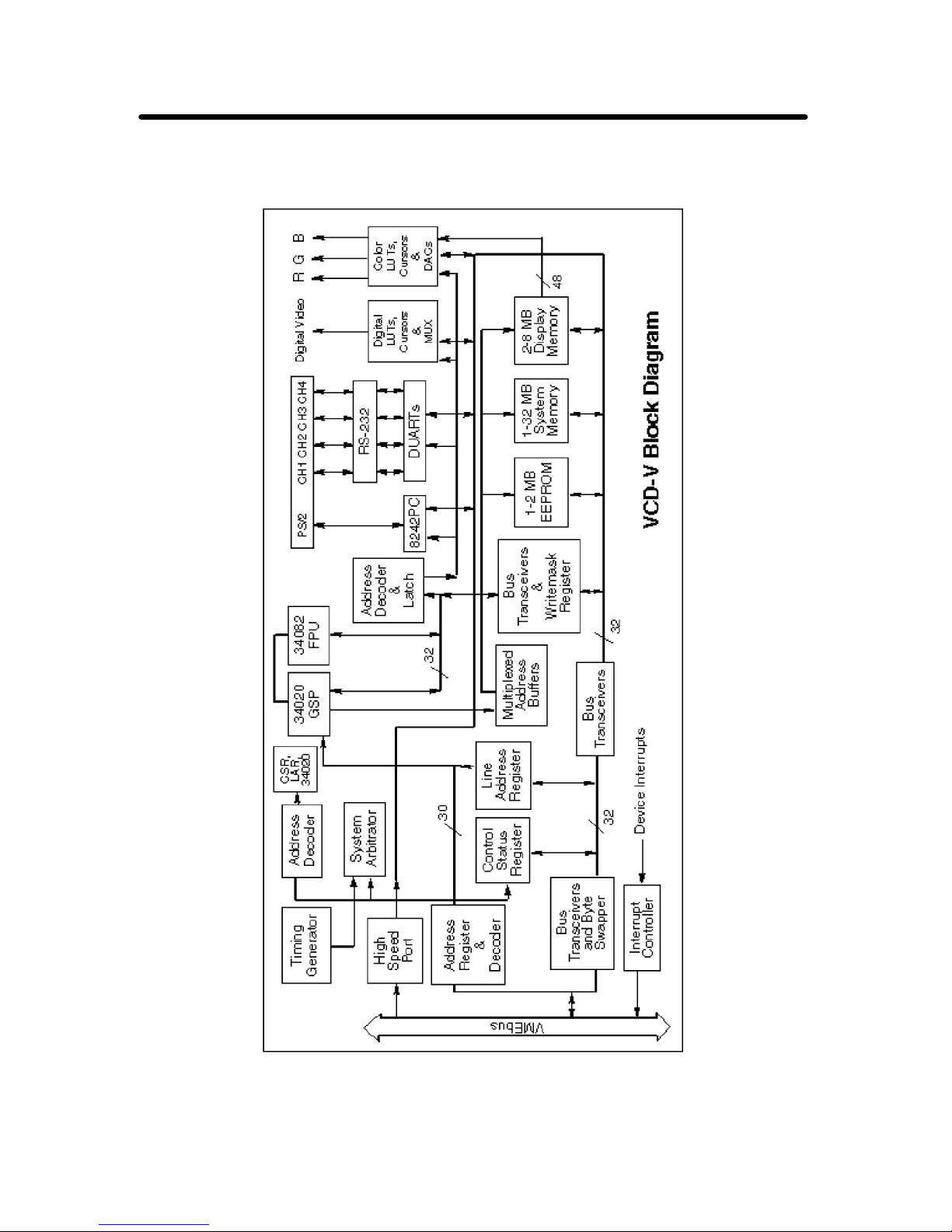
Peritek
Figure 4-1 VCD-V Block Diagram
Theory of Operation 4-15
Page 95
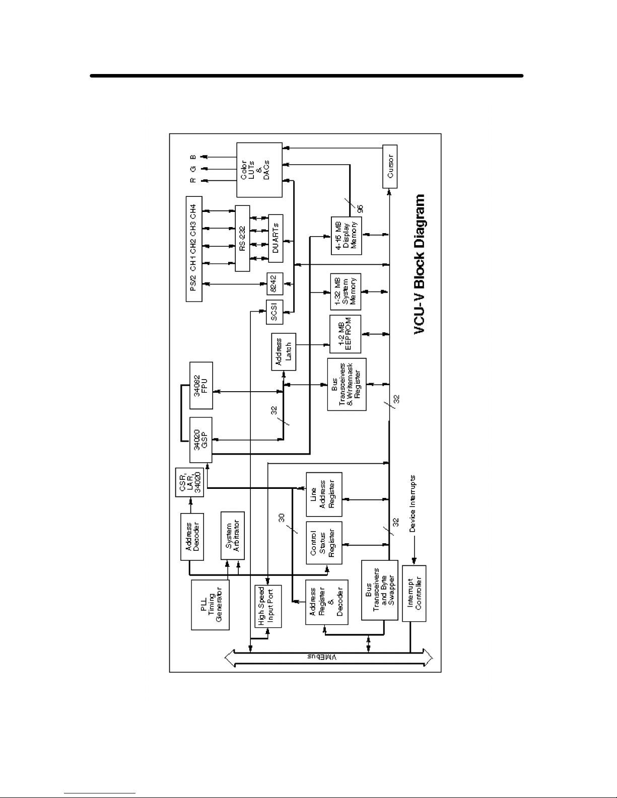
Peritek
Figure 4-2 VCU-V Block Diagram
4-16 Theory of Operation
Page 96
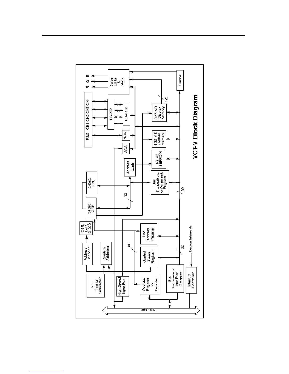
Peritek
Figure 4-3 VCT-V Block Diagram
Theory of Operation 4-17
Page 97

Chapter 5
Programming On-board
Devices and Memories
5.1 Introduction
As with the other chapters, this one covers the VCT-V, VCU-V, and
VCD-V. Most of the features are common, so the number of exceptions
does not get out of control. In the interest of reducing superfluous
information, and operating on the assumption that most users have either
PX Windows or CnP, this chapter has undergone some heavy duty editing.
In addition, the data sheet extracts which have heretofore been appended
to the manual have been removed, as they are little used. They are still
available upon request.
This chapter covers the special programming features of the individual
devices used on the graphics board. It is intended to supply information
unique to the board or to the application of a particular chip. Section 1.2
provides a list of appropriate publications which include manufacturer's
data sheets and manuals.
Peritek offers a variety of software to support the VCD-V, VCT-V, and
VCU-V in both Unix and real-time environments. Software includes
demo, test and initialization programs, a very comprehensive Graphics
Subroutine Package (generically CnP), and an X Windows X11R6 server
(PX Windows). These offerings are covered in detail in Chapter 3.
Programming On-board Devices and Memories 5-1
Page 98
Peritek
Note
Please read these sections before starting on this chapter:
Section 1.2 Functional description of the VCD-V, VCU-V, and
VCT-V graphics boards.
Sections 2.2-5 Installation.
Section 2.4 Jumper options.
Chapter 3 Summary of software support from Peritek.
Chapter 4 Theory of operation
This chapter includes the following sections:
5.1 Introduction
5.2 VMEbus and Control Registers
5.3 34020
5.4 Board Initialization Tables
5.5 Vertical and Horizontal Zoom Register
5.6 BT463 Lookup Table (VCT-V LUT)
5.7 BT468 Lookup Table (VCU-V LUT)
5.8 BT459 Lookup Table (VCD-V High Resolution Analog LUT)
5.9 BT482 Lookup Table (VCD-V Low Resolution Analog LUT)
5.10 Digital Lookup Table (VCD-V DLUT)
5.11 Hardware Cursors
5.12 2681 Serial I/O Ports (DUART)
5.13 5380 SCSI Port (VCT-V and VCU-V)
5.14 8242PC PC Keyboard Controller
5.15 High Speed Port (HSP)
5.16 Interrupts
5.17 Flash EEPROM and Serial EEPROM
5-2 Programming On-board Devices and Memories
Page 99

Peritek
5.2 VMEbus and Control Registers
The control registers and I/O window lie in a region of the VMEbus
address space reserved for peripheral devices and is usually to be found in
A16 space. The I/O window can also be placed in A24 space. Multiuser
operating systems (i.e. Unix) do not automatically allow a user to access
the VMEbus or physical memory. All Peritek software (including CnP
and PX Windows) include special mapping calls to give access to that
part of the VMEbus where the board addresses are located.
The VMEbus interface is implemented as a 1024 byte byte-addressable
raster line buffer (DBR) and a 4 word CSR group (16-bit word, long word
boundaries, VMEbus bits 0-15) in A16 space (the DBR can also be in A24
space - see Sections 5.2.1 and 5.2.4). For the sake of compatibility over
numerous CPUs and OS's (or as one might say, the lowest common
denominator) A16 space is the most general, and there is a minimal
performance impact for using the line buffer. Thus Peritek software
supports A16/A24 space addressing only. The standard addresses are
shown in Section 2.4.1. For linear address access to the entire board, it can
also respond to a 64 MB byte-addressable section of the 32-bit VMEbus
memory map, Contact Peritek for assistance in determining when it is
appropriate to use A32 space.
High speed VMEbus block transfers are supported for accesses to the A24
and A32 (64 MB block). Using the 34020's implied address mode, this
permits up to 64 long words to be transferred over the VMEbus with only
one address cycle. See 4.5 for more information.
Hardware byte swapping is now included in the graphics board. This can
be used to advantage in transferring large blocks of data between the bigendian VMEbus and the little-endian graphics board (see Section 5.3 for
more information.
Note
When byte swapping is enabled the 1KB line buffer expands to 4KB
and the 64 MB block expands to 256 MB.
Programming On-board Devices and Memories 5-3
Page 100

Peritek
The CSR group consists of 4 registers:
Relative Register Section
Offset Mnemonic Description Reference
0 CSR General Control 5.2.1
4 LAR Line Address Register 5.2.2
8 XARADR A32 Address Match Register 5.2.3
DBRADR A16/A24 Address Match Register 5.2.4
C VECADR Interrupt Vector Address Register 5.2.5
The XAR/DBRADR and VECADR registers allow all VMEbus address
areas to which the board responds to be programmable except for the CSR
base address, which is (necessarily) jumper selected from 16 different
combinations (see Section 2.4.1).
Note
CSR group registers should be accessed as words, not long words,
because the high word will not read back useful data.
5.2.1 Control/Status Register (CSR)
Table 5-1 CSR Bit Summary
Bit Mnemonic Function R/W Reset
15 spare was BIGEND, now reads back 0 no no
14 REVFLAG was r/w, now read back set no no
8-13 spare not used, reads back 0 no no
7 A24EN clear = A16 DBR access,
set = A24 DBR access yes sysreset
6 CRTCON turns on the 34020 yes sysreset
5 MEMON enables the DBR addresses yes sysreset
4 XMEMON Enables 32-bit address response. yes sysreset
3 A1624SWAPEN Enables A16 and A24 swap mode yes sysreset
2 VINTEN VMEbus interrupt enable yes sysreset
1 A32SWAP Enables A32 swap mode yes sysreset
0 XARSEL Select XAR register access yes sysreset
5-4 Programming On-board Devices and Memories
 Loading...