

2
查询PI6C2502供应商
234567890123456789012345678901212345678901234567890123456789012123456789012345678901234567890121234567890123456789012345678901212345678901
PI6C2502
Phase-Locked Loop Clock Driver
Product Features
• High-Performance Phase-Locked-Loop Clock Distribution
for Networking,
• Synchronous DRAM modules for server/workstation/
PC applications
• Allows Clock Input to have Spread Spectrum
modulation for EMI reduction
• Zero Input-to-Output delay
• Low jitter: Cycle-to-Cycle jitter ±100ps max.
• On-chip series damping resistor at clock output drivers
for low noise and EMI reduction
• Operates at 3.3V V
• Wide range of Clock Frequencies up to 80 MHz
• Package: Plastic 8-pin SOIC Package (W)
CC
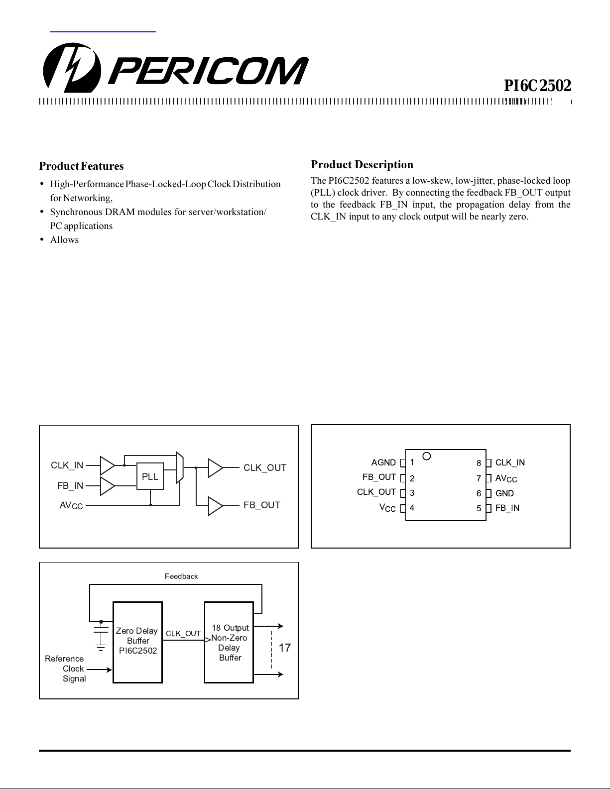
Product Description
The PI6C2502 features a low-skew, low-jitter, phase-locked loop
(PLL) clock driver. By connecting the feedback FB_OUT output
to the feedback FB_IN input, the propagation delay from the
CLK_IN input to any clock output will be nearly zero.
Application
If a system designer needs more than 16 outputs with the features
just described, using two or more zero-delay buffers such as
PI6C2509Q, and PI6C2510Q, is likely to be impractical. The
device-to-device skew introduced can significantly reduce the
performance. Pericom recommends the use of a zero-delay buffer
and an eighteen output non-zero-delay buffer. As shown in Figure
1, this combination produces a zero-delay buffer with all the signal
characteristics of the original zero-delay buffer, but with as many
outputs as the non-zero-delay buffer part. For example, when
combined with an eighteen output non-zero delay buffer, a system
designer can create a seventeen-output zero-delay buffer.
Logic Block Diagram
CLK_IN
FB_IN
AV
CC
Zero Delay
Buffer
Reference
Clock
Signal
PI6C2502
PLL
Feedback
CLK_OUT
18 Output
Non-Zero
V
Delay
Buffer
CLK_OUT
FB_OUT
17
Product Pin Configuration
CC
1
2
3
4
AGND
FB_OUT
CLK_OUT
V
8-Pin
W
8
7
6
5
CLK_IN
AV
CC
GND
FB_IN
Figure 1. This Combination Provides Zero-Delay Between the
Reference Clocks Signal and 17 Outputs
1
PS8382B 03/20/02
Pin Functions
emaNniPrebmuNniPepyTnoitpircseD
NI_KLC8I .tupnikcolCecnerefeRNI_KLC.tupnikcolcmurtcepsdaerpsswolla
NI_BF5I .tupnikcabdeeFNI_BF.LLPlanretniehtotlangiskcabdeefehtsedivorp
TUO_BF2O
PI6C2502
Phase-Locked Loop Clock Driver
tuptuokcabdeeFTUO_BF.kcabdeeflanretxerofdetacidedsi
eulavemasehtforotsisergnipmad-seiresdeddebmenasahTUO_BF
stuptuokcolcehtsa.TUO_KLC
TUO_KLC3O
VA.ylppusrewopgolanA
CC
VA
CC
7rewoP
VAnehW.sesopruptset
CC
dnaNI_KLC.stuptuoecivedehtotyltceriddereffubsi
DNGA1dnuorG .yrtiucricgolanaehtrofecnereferdnuorgehtsedivorpDNGA.dnuorggolanA
V
CC
4rewoP.ylppusrewoP
DNG6 dnuorG.dnuorG
DC Specifications (Absolute maximum ratings over operating free-air temperature range)
lobmySretemaraP.niM.xaMstinU
V
I
V
O
I
CD_O
T
GTS
rewoPTtanoitapissidrewopmumixaM
egnaregatlovtupnI
egnaregatlovtuptuO
tnerructuptuoCD 001Am
o
55=
A
riallitsniC0.1W
erutarepmetegarotS56051
foseipocweks-woledivorpstuptuoesehT.stuptuokcolC.NI_KLC
.rotsisergnipmad-seiresdeddebmenasahtuptuohcaE
5.0V
5.0+V
CC
rofLLPehtssapybotdesuoslaebnac
dessapybsiLLP,dnuorgotdeppartssi
o
C
Note: Stress beyond those listed under absolute maximum ratings may cause permanent damage to the device.
retemaraPsnoitidnoCtseTV
I
CC
C
I
VIV=
VIV=
CC
CC
I;DNGro
DNGro
)1(
0=
O
CC
V6.301
.niM.pyT.xaMstinU
4
V3.3
C
O
VOV=
CC
DNGro6
Note: 1. Continuous Output Current
2
µA
Fp
PS8382B 03/20/02
12345678901234567890123456789012123456789012345678901234567890121234567890123456789012345678901212345678901234567890123456789012123456789012
12345678901234567890123456789012123456789012345678901234567890121234567890123456789012345678901212345678901234567890123456789012123456789012
Recommended Operating Conditions
lobmySretemaraP.niM.xaMstinU
PI6C2502
Phase-Locked Loop Clock Driver
V
CC
V
HI
V
LI
V
I
T
A
egatlovylppuS0.36.3
egatlovtupnilevelhgiH0.2
egatlovtupnilevelwoL 8.0
egatlovtupnI0V
erutarepmetria-eerfgnitarepO007Cº
Electrical Characteristics
(Over recommended operating free-air temperature range Pull Up/Down Currents, VCC = 3.0V)
lobmySretemaraPnoitidnoC.niM.xaMstinU
I
HO
tnerrucpu-lluP
V
V
V
I
LO
tnerrucnwod-lluP
V
V4.2=
TUO
V0.2=
TUO
V8.0=52
TUO
TUO
V55.0=71
AC Specifications Timing Requirements
(Over recommended ranges of supply voltage and operating free-air temperature)
lobmySretemaraP.niM.xaMstinU
V
CC
− 81
− 03
Am
F
D
CLK
CYI
ycneuqerfkcolC5208zHM
elcycytudkcolctupnI0406%
purewopretfaemiTnoitazilibatS1sm
Switching Characteristics
(Over recommended ranges of supply voltage and operating free-air temperature, CL=30pF)
retemaraP)tupnI(morF)tuptuO(oT
rettijtuohtiwrorreesahptNI_KLC ↑ zHM66dnazHM001taNI_BF ↑ 051051+
elcyc-ot-elcyc,rettiJzHM66dnazHM001tATUO_KLC001001+
zHM001tawekS
zHM66dna
TUO_KLCroTUO_BF
elcycytuD
V0.2otV4.0,emit-esir,rt 0.1
V4.0otV0.2,emit-llaf,ft 1.1
Note: These switching parameters are guaranteed by design.
TUO_KLC
TUO_BFro
TUO_KLC
TUO_BFro
V
CC
C°07-0,V3.0±V3.3=stinU
.niM.pyT.xaM
sp
002
5455%
sn
3
PS8382B 03/20/02
Application Note
Layout and Schematic Guidelines
Introduction
Because of todays high-speed design demands, board designers
must have extensive knowledge concerning transmission line
effect, EMI, and crosstalk. They also need to understand board
materials, signal and power stacking, connectors, cables, vias, and
trace dimensions. Pericom Semiconductor Corporation offers an
extensive line of high-speed clock products for desktop, notebook,
set top boxes, information device, servers, and workstations. To
make high-speed chips function properly, a designer needs to rely
on accurate schematics and layout guidelines.
This application note focuses on Pericoms PI6C2502 Zero- Delay
Clock Buffer, presenting schematics and layout guidelines for the
chip. Also listed are some decoupling guidelines that are important
for this chips varied applications.
Decoupling Capacitors
Every printed circuit board needs large bypass capacitors to
balance the inductance of the power-supply wiring. These capacitors have some lead inductance that increase as the frequency goes
higher, which is why it is very important to place the capacitors as
close as possible to the V
To reduce the series lead inductance effect, avoid the following:
1. Long traces larger than 0.01 inch between capacitor pad and via
2. Use of capacitors other than surface mount
3. Via holes less than 0.035-inch diameter
Pericoms clocks use high-precision, integrated analog PLL that can
be effected by the power supply and ground pins. Noise on these
two pins can dramatically increase skew and output jitter.
To minimize these problems, connect a 4.7µF, a 220nF , and a 2.2nF
capacitor to the digital supply pin. Also use one 4.7µF , one 220nF,
and one 2.2nF capacitor on the analog supply pin. Connect the other
side to the analog ground pin.
Place a 10µF capacitor from the main power island to the power plane
that is supplied to the clock chip.
Use high-quality, low ESR, ceramic surface-mount capacitors.
and Ground Pins on the Chip.
CC
PI6C2502
Phase-Locked Loop Clock Driver
This location minimizes the total loops needed between the outgoing and returning paths. That is why it is important to separate the
signal layers by ground planes if possible. Also avoid totally
cutting part of the ground plane to be used for a signals path. That
is totally unacceptable, because it will increase crosstalk considerably and does not provide a clean return to those signals. Also use
lower trace impedance because it lowers undershoot and overshoot. Always use FR-4 material for board fabrication. Use 4- layer
stack-up arrangement. Make sure you have a signal layer that is
followed by the ground layer, then a power layer, and finally the
second signal layer. Please see Figure 1 below.
CORE
Clock
Primary Signal
Layer (½ oz. cu.)
Ground Plane
(1 oz. cu.)
Power Plane
(1 oz. cu.)
Secondary Signal
Layer (½ oz. cu.)
Z = 60 Ohms
5 mils
47 mils
5 mils
Z = 60 Ohms
PREPREG
PREPREG
Total Board Thickness = 62.6
Figure 1: Four-Layer Board Stack-up
Clock routing and spacing
To minimize crosstalk on the clock signals, use a minimum of
0.014-inch spacing between clock traces and others. If you have to
use serpentine to match trace lengths on similar chips, make sure
that you have at least 0.018-inch spacing for serpentines. Please see
Figure 2 below.
0.014"
Stacking
At low speeds, currents follow the least resistance path, but at high
speeds current follows the least inductance path. The lowest
inductance return path lies directly under the signal conductor.
0.018"
Figure 2: Clock Trace Spacing Guidelines
4
PS8382B 03/20/02

Schematic Drawing
PI6C2502
Phase-Locked Loop Clock Driver
3.3V
Power
Supply
1.5µH
Clock Chip Layout
4.7µF
.22µF
PI6C2502
AGND
FB_OUT
CLK_OUT
.002µF
VCC
Decoupling Capacitors
Series Terminating Resistor
PI6C2502
CLK_IN
AVCC
GND
FB_IN
INPUT_CLOCK
25-150 MHZ
4.7µF
5-12pF
Feedback
Capacitor
AVCC Island for PI6C2510
.22µF
.002µF
1.5µH
Board
AVCC
GND
AGND
FB_OUT
R
C
C
C
L
VCC
CLK_OUT
Use Wider Traces for Ground and Power
(0.034-inch width, 0.1-inch pitch)
Legend:
GND = Via to Digital Ground
AGND = Via to Analog Ground
VCC = Via to 3.3V Digital Power
AVCC = Via to 3.3V Analog Power
R = Termination Resistor 12-32Ω
C = Decoupling Capacitor
L = Inductor
CFB = Feedback Capacitor
GND
FB_IN
AVCC
L
CFB
C
C
C
5
CLK_IN
AGND
AGND
AGND
GND
PS8382B 03/20/02
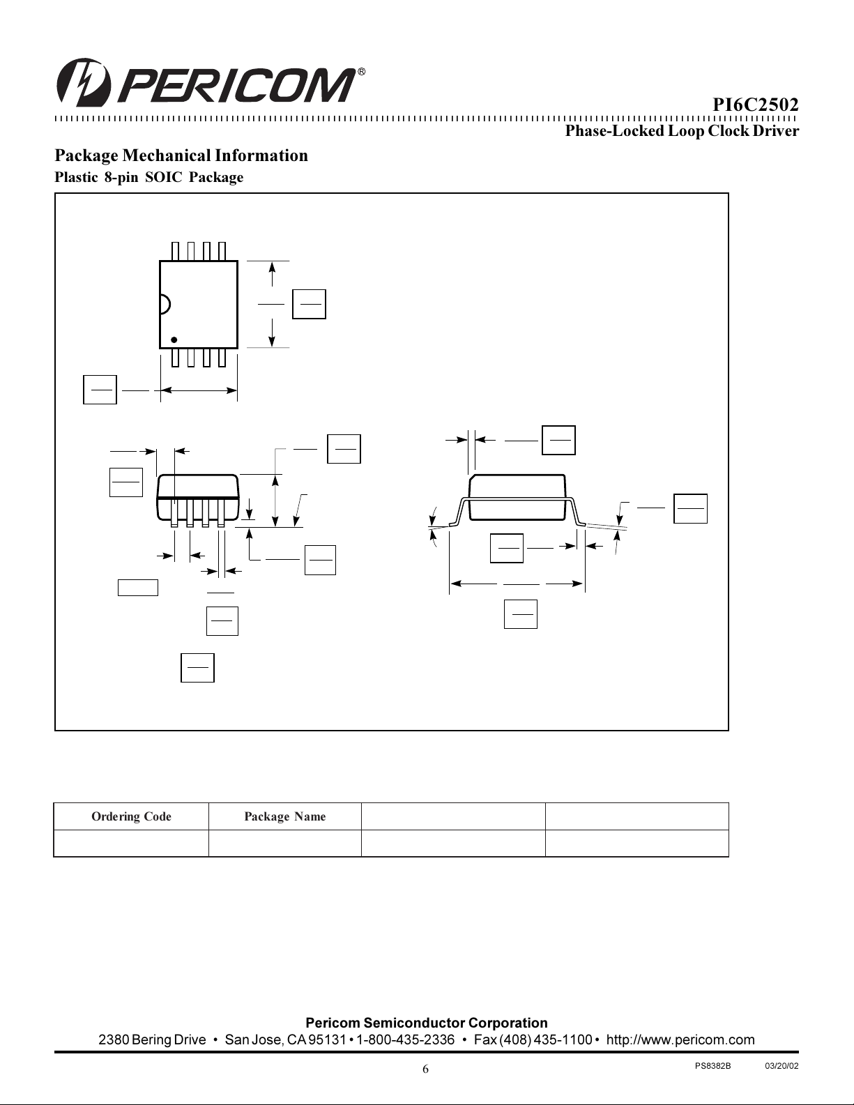
Package Mechanical Information
Plastic 8-pin SOIC Package
8
.149
.157
PI6C2502
Phase-Locked Loop Clock Driver
3.78
3.99
4.80
5.00
REF
.189
.196
.016
.026
0.406
0.660
.050
BSC
1.27
1
X.XX
X.XX
.053
.068
.0040
.0098
.013
.020
0.330
0.508
DENOTES DIMENSIONS
IN MILLIMETERS
1.35
1.75
SEATING PLANE
0.10
0.25
0-8˚
.0099
.0196
0.40
1.27
.2284
.2440
5.80
6.20
.016
.050
0.25
0.50
x 45˚
.0075
.0098
0.19
0.25
Ordering Information
edoCgniredrOemaNegakcaPepyTegakcaPegnaRgnitarepO
W2052C6IP8WCIOSlim-051nip-8laicremmoC
2380 Bering Drive San Jose, CA 95131 1-800-435-2336 Fax (408) 435-1100 http://www.pericom.com
Pericom Semiconductor Corporation
6
PS8382B 03/20/02
 Loading...