


V
DD_A
V
SS_A
I
REF
LOCK
OE_7
OE_4
OUT7
OUT7#
OE_INV
V
DD
OUT6
OUT6#
OE_6
OE_5
OUT5
OUT5#
V
SS
V
DD
OUT4
OUT4#
PLL_BW#
SRC_STOP#
PWRDWN#
V
SS
48
47
46
45
44
43
42
41
40
39
38
37
36
35
34
33
32
31
30
29
28
27
26
25
1
2
3
4
5
6
7
8
9
10
11
12
13
14
15
16
17
18
19
20
21
22
23
24
SRC_DIV#
V
DD
V
SS
SRC
SRC#
OE_0
OE_3
OUT0
OUT0#
VSS
V
DD
OUT1
OUT1#
OE_1
OE_2
OUT2
OUT2#
V
SS
V
DD
OUT3
OUT3#
PLL/BYPASS#
SCLK
SDA
07-0237
查询PI6C20800SVE供应商
PI6C20800S
PCI Express 1:8
HCSL Clock Buffer
Features
• Phase jitter fi lter for PCIe application
• Eight Pairs of Differential Clocks
• Low skew < 50ps
• Low Cycle-to-cycle jitter < 50ps
• Output Enable for all outputs
• Outputs Tristate control via SMBus
• Power Management Control
• Programmable PLL Bandwidth
• PLL or Fanout operation
• 3.3V Operation
• Packaging (Pb-Free & Green):
— 48-Pin SSOP (V)
— 48-Pin TSSOP (A)
Block Diagram
PLL/BYPASS#
OE_INV
OE [0:7]
SRC_STOP#
PWRDWN#
SCLK
SDA
SRC_DIV#
SRC
SRC#
PLL_BW#
Output
Control
SMBus
Controller
PLL
DIV
OUT0
OUT0#
OUT1
OUT1#
OUT2
OUT2#
OUT3
OUT3#
OUT4
OUT4#
OUT5
OUT5#
OUT6
OUT6#
OUT7
OUT7#
LOCK
Description
PI6C20800S is a PCI Express, high-speed, low-noise differential
clock buffer designed to be a companion to PI6C410BS PCI
Express clock generator for Intel server chipsets. The device
distributes the differential SRC clock from PI6C410BS to eight
differential pairs of clock outputs either with or without PLL.
The input SRC clock can be divided by 2 when SRC_DIV# is
LOW. The clock outputs are controlled by input selection of
SRC_STOP#, PWRDWN# and SMBus, SCLK and SDA. When
input of either SRC_STOP# or PWRDWN# is LOW, the output
clocks are Tristated. When PWRDWN# is LOW, the SDA and
SCLK inputs must be Tristated.
Pin Confi guration
1
PS8887B 10/19/07

PI6C20800S
07-0237
PCI Express 1:8
HCSL Clock Buffer
Pin Descriptions
Pin Name
SRC_DIV# Input 1
SRC & SRC# Input 4, 5 0.7V Differential SRC input from PI6C410 clock synthesizer
OE [0:7] Input
OE_INV Input 40
OUT[0:7] & OUT[0:7]# Output
PLL/BYPASS# Input 22 3.3V LVTTL input for selecting fan-out of PLL operation.
SCLK Input 23 SMBus compatible SCLOCK input
SDA I/O 24 SMBus compatible SDATA
I
REF
SRC_STOP# Input 27 3.3V LVTTL input for SRC stop, active LOW
PLL_BW# Input 28 3.3V LVTTL input for selecting the PLL bandwidth
PWRDWN# Input 26 3.3V LVTTL input for Power Down operation, active LOW
LOCK Output 45
V
DD
V
SS
V
SS_A
V
DD_A
Type Pin # Descriptions
3.3V LVTTL input for selecting input frequency divide by 2,
active LOW.
6, 7, 14, 15, 35, 36,
43, 44
3.3V LVTTL input for enabling outputs, active HIGH.
3.3V LVTTL input for inverting the OE, SRC_STOP# and
PWRDWN# pins.
When 0 = same stage
When 1 = OE[0:7], SRC_STOP#, PWRDWN# inverted.
8, 9, 12, 13, 16 17,
20, 21, 29, 30, 33, 34,
0.7V Differential outputs
37, 38, 41, 42
Input 46 External resistor connection to set the differential output current
3.3V LVTTL output, transition high when PLL lock is achieved
(Latched output)
Power 2, 11, 19, 31, 39 3.3V Power Supply for Outputs
Ground 3, 10, 18, 25, 32 Ground for Outputs
Ground 47 Ground for PLL
Power 48 3.3V Power Supply for PLL
Serial Data Interface (SMBus)
PI6C20800S is a slave only SMBus device that supports indexed block read and indexed block write protocol using a single 7-bit
address and read/write bit as shown below.
Address assignment
A6 A5 A4 A3 A2 A1 A0 R/W
110 1 1 1 0 0/1
Slave
Addr
(1)
R/W Ack
Register
offset
Ack
Byte
Count
= N
Ack
2
Data
Byte 0
Ack
Data
Byte N
- 1
Ack
Stop
bit
PS8887B 10/19/07
Data Protocol
1 bit 7 bits 1 1 8 bits 1 8 bits 1 8 bits 1 8 bits 1 1 bit
Start
bit
Note:
1. Register offset for indicating the starting register for indexed block write and indexed block read. Byte Count in write mode cannot be 0.

PI6C20800S
07-0237
PCI Express 1:8
HCSL Clock Buffer
Data Byte 0: Control Register
Bit Descriptions Type Power Up Condition Output(s) Affected Pin
SRC_DIV#
0
0 = Divide by 2
1 = Normal
PLL/BYPASS#
1
0 = Fanout
1 = PLL
PLL Bandwidth
2
0 = HIGH Bandwidth,
1 = LOW Bandwidth
3 RESERVED
4 RESERVED
5 RESERVED
SRC_STOP#
6
0 = Driven when stopped
1 = Tristate
PWRDWN#
7
0 = Driven when stopped
1 = Tristate
RW 1 = x1 OUT[0:7], OUT[0:7]# NA
RW 1 = PLL OUT[0:7], OUT[0:7]# NA
RW 1 = Low OUT[0:7], OUT[0:7]# NA
RW 0 = Driven when stopped OUT[0:7], OUT[0:7]#
RW 0 = Driven when stopped OUT[0:7], OUT[0:7]# NA
Data Byte 1: Control Register
Bit Descriptions Type Power Up Condition Output(s) Affected Pin
0
1 RW 1 = Enabled OUT1, OUT1# NA
2 RW 1 = Enabled OUT2, OUT2# NA
3 RW 1 = Enabled OUT3, OUT3# NA
4 RW 1 = Enabled OUT4, OUT4# NA
5 RW 1 = Enabled OUT5, OUT5# NA
6 RW 1 = Enabled OUT6, OUT6# NA
7 RW 1 = Enabled OUT7, OUT7# NA
OUTPUTS enable
1 = Enabled
0 = Disabled
RW 1 = Enabled OUT0, OUT0# NA
3
PS8887B 10/19/07
PI6C20800S
07-0237
PCI Express 1:8
HCSL Clock Buffer
Data Byte 2: Control Register
Bit Descriptions Type Power Up Condition Output(s) Affected Pin
0
1 RW 0 = Free running OUT1, OUT1# NA
2 RW 0 = Free running OUT2, OUT2# NA
Allow control of OUTPUTS with
3 RW 0 = Free running OUT3, OUT3# NA
assertion of SRC_STOP#
0 = Free running
4 RW 0 = Free running OUT4, OUT4# NA
1 = Stopped with SRC_Stop#
5 RW 0 = Free running OUT5, OUT5# NA
6 RW 0 = Free running OUT6, OUT6# NA
7 RW 0 = Free running OUT7, OUT7# NA
RW 0 = Free running OUT0, OUT0# NA
Data Byte 3: Control Register
Bit Descriptions Type Power Up Condition Output(s) Affected Pin
0
1RW
2RW
3RW
RESERVED
4RW
5RW
6RW
7RW
RW
Data Byte 4: Pericom ID Register
Bit Descriptions Type Power Up Condition Output(s) Affected Pin
0
1R0NANA
2R0NANA
3R0NANA
4R0NANA
5R1NANA
6R0NANA
7R0NANA
Pericom ID
R 0 NA NA
4
PS8887B 10/19/07

PCI Express 1:8
07-0237
HCSL Clock Buffer
Functionality
PWRDWN# OUT OUT# SRC_Stop# OUT OUT#
1 Normal Normal 1 Normal Normal
0I
× 2 or Float LOW 0 I
REF
× 6 or Float LOW
REF
Power Down (PWRDWN# assertion)
PI6C20800S
PWRDWN#
OUT
OUT#
Power Down (PWRDWN# De-assertion)
Tstable
<1ms
OUT
OUT#
Tdrive_PwrDwn#
<300us, >200mV
Figure 2. Power down de-assert sequence
PWRDWN#
Figure 1. Power down sequence
5
PS8887B 10/19/07
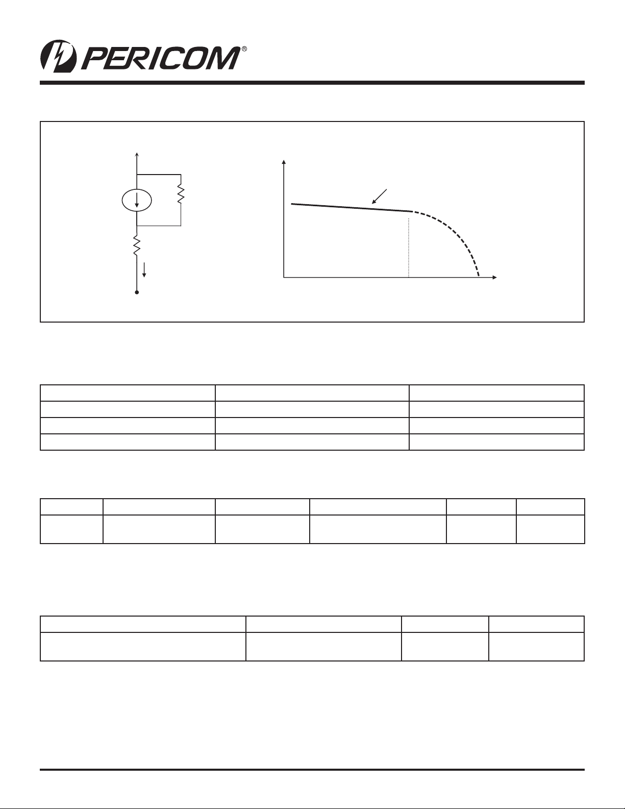
Current-mode output buffer characteristics of OUT[0:7], OUT[0:7]#
07-0237
V
DD
(3.3V ± 5%)
Slope ~ 1/Rs
R
O
I
OUT
R
OS
Iout
V
= 0.85V max
OUT
Figure 9. Simplifi ed diagram of current-mode output buffer
0V
PI6C20800S
PCI Express 1:8
HCSL Clock Buffer
0.85V
Differential Clock Buffer characteristics
Symbol Minimum Maximum
V
R
R
O
OS
OUT
3000Ω N/A
unspecifi ed unspecifi ed
N/A 850mV
Current Accuracy
Symbol Conditions Confi guration Load Min. Max.
R
Note:
1. I
I
OUT
NOMINAL
= 475Ω 1%
VDD = 3.30 ±5%
refers to the expected current based on the confi guration of the device.
REF
I
REF
= 2.32mA
Nominal test load for given
confi guration
-12%
I
NOMINAL
Differential Clock Output Current
Board Target Trace/Term Z Reference R, Iref = VDD/(3xRr) Output Current VOH @ Z
100Ω
(100Ω differential ≈ 15% coupling ratio)
R
= 475Ω 1%,
REF
I
= 2.32mA
REF
IOH = 6 x I
REF
0.7V @ 50
+12%
I
NOMINAL
6
PS8887B 10/19/07
PI6C20800S
07-0237
PCI Express 1:8
HCSL Clock Buffer
Absolute Maximum Ratings
(1)
(Over operating free-air temperature range)
Symbol Parameters Min. Max. Units
V
DD_A
V
V
V
DD
IH
IL
3.3V Core Supply Voltage -0.5 4.6
3.3V I/O Supply Voltage -0.5 4.6
Input HIGH Voltage 4.6
Input LOW Voltage -0.5
Ts Storage Temperature -65 150 °C
V
ESD
Note:
1. Stress beyond those listed under “Absolute Maximum Ratings” may cause permanent damage to the device.
DC Electrical Characteristics (V
ESD Protection 2000 V
= 3.3±5%, V
DD
DD_A
= 3.3±5%)
Symbol Parameters Condition Min. Max. Units
V
V
V
V
V
V
I
C
C
L
I
DD_A
DD
IH
IL
I
IK
OH
OL
OH
IN
OUT
PIN
DD
SS
I
SS
T
A
3.3V Core Supply Voltage 3.135 3.465
3.3V I/O Supply Voltage 3.135 3.465
3.3V Input HIGH Voltage V
DD
2.0 VDD + 0.3
3.3V Input LOW Voltage VSS – 0.3 0.8
Input Leakage Current 0 < VIN < V
DD
-5 +5 μA
3.3V Output HIGH Voltage IOH = -1mA 2.4
3.3V Output LOW Voltage IOL = 1mA 0.4
Output HIGH Current
IOH = 6 x I
I
= 2.32mA
REF
REF
,
12.2
15.6
Logic Input Pin Capacitance 1.5 5
Output Pin Capacitance 6
Pin Inductance 7 nH
Power Supply Current VDD = 3.465V, F
= 100MHz 250
CPU
Power Down Current Driven outputs 80
Power Down Current Tristate outputs 12
Ambient Temperature 0 70 °C
V
V
V
mA
pF
mAI
7
PS8887B 10/19/07

PI6C20800S
07-0237
PCI Express 1:8
HCSL Clock Buffer
AC Switching Characteristics
(1,2,3)
(V
DD
= 3.3±5%, V
DD_A
= 3.3±5%)
Symbol Parameters Min Max. Units Notes
SRC/SRC# Input Frequency PLL Mode 100 MHz 6
SRC/SRC# Input Frequency Bypass Mode 100 400 MHz 6
Rise and Fall Time (measured between 0.175V to 0.525V) 175 700
fall
/
Rise and Fall Time Variation 125 2
Input to Output Propagation Delay
PLL Mode -250 250 ps
Bypass Mode 2.5 6.5 ns
Output-to-Output Skew 50 ps 3
Voltage HIGH (Measured at 100MHz @ 3.3V) 660 850
Max. Voltage 1150
Min. Voltage -300
Voltage LOW -150 +150 2
Absolute crossing poing voltages 250 550 2
Total Variation of V
over all edges 140 2
cross
Duty Cycle (Measured at 100 MHz) 45 55 % 3
ps
mV
T
rise
ΔT
ΔT
T
V
V
V
V
V
ΔV
F
in
/ T
rise
fall
T
pd
skew
HIGH
OVS
UDS
LOW
cross
cross
T
DC
Jitter, Cycle-to-cycle (PLL Mode, Measurement for differential
T
jcyc-cyc
waveform)
50 ps 4
Jitter, Cycle-to-cycle (BYPASS mode as additive jitter)
J
add
Notes:
1. Test confi guration is RS = 33.2Ω, Rp = 49.9Ω, and 2pF.
2. Measurement taken from Single Ended waveform.
3. Measurement taken from Differential waveform.
4. Measured using M1 timing analyzer from Amherst.
5. Additive jitter is calculated from input and output RMS phase jitter by using PCIe Gen II fi lter. (J
6. –0.5% downnspread input
Additive RMS phase jitter for PCIe GenII <0 1 ps 5
= √ (output jitter)2 – (input jitter)
add
2
2
2
)
Confi guration Test Load Board Termination
Rs
33Ω
5%
PI6C20800
475Ω
1%
Rs
33Ω
5%
Rp
49.9Ω
1%
Rp
49.9Ω
1%
8
TLA
TLB
2pF
5%
OUT
OUT#
2pF
5%
PS8887B 10/19/07
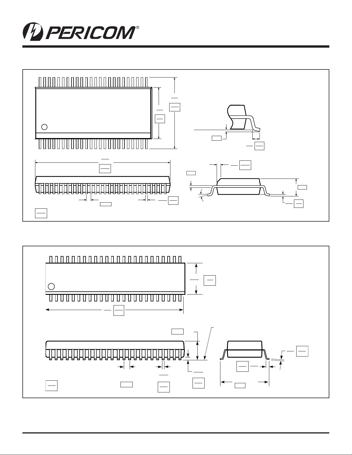
Packaging Mechanical: 48-Pin SSOP (V)
07-0237
48
1
.620
.630
15.75
16.00
.291
.299
7.39
7.59
.395
.420
10.03
10.67
Gauge Plane
.008
0.20
Nom.
.010
0.25
.015
.025
0.381
0.635
.02
.04
0.51
1.01
x 45˚
PI6C20800S
PCI Express 1:8
HCSL Clock Buffer
.110 2.79
Max
.025 BSC
0.635
X.XX
DENOTES DIMENSIONS
X.XX
IN MILLIMETERS
Packaging Mechanical: 48-Pin TSSOP (A)
48
1
X.XX
DENOTES DIMENSIONS
X.XX
IN MILLIMETERS
.488
.496
12.4
12.6
.0197
BSC
0.50 0.17
.008
.0135
.007
.010
0.27
0.20
0.34
.047
1.20 Max
.236
.244
.002
.006
0.05
0.15
0-8˚
6.0
6.2
SEATING PLANE
0.45
0.75
.319
8.1
.018
.030
BSC
.008
.016
.004
.008
0.20
0.40
0.09
0.20
9
PS8887B 10/19/07

PI6C20800S
07-0237
PCI Express 1:8
HCSL Clock Buffer
Ordering Information
(1,2)
Ordering Code Package Code Package Description
PI6C20800SVE VE 48-pin, 300-mil wide, SSOP, Pb-Free and Green
PI6C20800SAE AE 48-pin, 240-mil wide, TSSOP, Pb-Free and Green
Notes:
1. Thermal characteristics can be found on the company web site at www.pericom.com/packaging/
2. E = Pb-free and Green
Pericom Semiconductor Corporation • 1-800-435-2336 • www.pericom.com
10
PS8887B 10/19/07
 Loading...