

Datasheet PI5A121CEX, PI5A121TEX, PI5A121TX, PI5A122CEX, PI5A122TEX Datasheet (Pericom) [ru]
...
PI5A121/PI5A122/PI5A124
PI5A121 PI5A122 PI5A124
2
3
1
NO
GND IN
V+
5
4
COM IN
2
3
1
NC
GND IN
V+
5
4
2
3
1
V+
GND
SOT23-6
NC
NO
COM
5
6
4
SOT23-5
SC70-5
SOT23-5
SC70-5
09-0002
Wide Bandwidth Analog Switches
Features
• Single-Supply Operation (+2V to +6V)
• Rail-to-Rail Analog Signal Dynamic Range
• Low On-Resistance (6Ω typ. with 5V supply)
Minimizes Distortion and Error Voltages
• On-Resistance Flatness, 3Ω typ.
• Low Charge Injection Reduces Glitch Errors. Q = 4pC typ.
• High Speed. t
= 10ns typ.
ON
• Wide -3dB Bandwidth: 326 MHz (typ.)
• High-Current Channel Capability: >100mA
• TTL/CMOS Logic Compatible
• Low Power Consumption (0.5µW typ)
• Small outline transistor package minimizes board area
• Packaging (Pb-free & Green available):
- 5-pin 65-mil wide SOT23 (T) for PI5A121 and PI5A122
- 6-pin 65-mil wide SOT23 (T) for PI5A124
- 5-pin 50-mil wide SC70 (C) for PI5A121/PI5A122
Applications
• Audio, Video Switching, and Routing
• Battery-Powered Communication Systems
• Computer Peripherals
• Telecommunications
• Portable Instrumentation
• Mechanical Relay Replacement
• Cell Phones
• PDAs
Description
The PI5A121/PI5A122/PI5A124 are analog switches designed
for single-supply operation. These high-precision devices are
ideal for low-distortion audio, video, signal switching and routing.
The PI5A121 is a single-pole throw (SPST) normally open (NO)
switch. The switch is open when IN is LOW. The PI5A122 is
a single-pole single-throw (SPST) normally closed (NC) switch.
Each switch conducts current equally well in either direction
when on. When off, they block voltages up to V+.
These switches are fully specied with +5V, and +3.3V supplies.
With +5V, they guarantee <10Ω On-Resistance. On-Resistance
matching between channels is within 2Ω. On-Resistance atness
is less than 55Ω over the specied range. These switches also
guarantee fast switching speeds (tON <20ns).
These products are available in 5-pin SC70 and/or 6-pin SOT23
plastic packages for operation over the industrial (-40
temperature range.
o
C to +85oC)
Functional Diagrams, Pin Congurations and Truth Tables
IN PI5A121 PI5A122
Switches shown for Logic “0” input
0 OFF ON
1 ON OFF
1
PI5A124
LOGIC NC NO
0 ON OFF
1 OFF ON
PS8203H 10/23/09

PI5A121/PI5A122/PI5A124
09-0002
Wide Bandwidth Analog Switch
Absolute Maximum Ratings
Voltages Referenced to Gnd
V+ ..........................................................................-0.5V to +7V
VIN, V
or 30mA, whichever occurs rst
Current (any terminal) ..................................................... ±25mA
Peak Current, COM, NO, NC
(Pulsed at 1ms, 10% duty cycle) ..................................... ±25mA
Caution: Stresses beyond those listed under “Absolute Maximum Ratings” may cause permanent damage to the device. This is a stress only rating
and operation of the device at these or any other conditions beyond those indicated in the operational sections of this specication is not implied.
, VNC, VNO (Note 1) ...................-0.5V to VCC +2V
COM
Thermal Information
Continuous Power Dissipation
SOT23-6 (derate 7mW/ºC above +70ºC) ........................ 550mW
Storage Temperature .........................................-65ºC to +150ºC
Lead Temperature (soldering, 10s) ................................. +300ºC
Note 1:
Signals on NC, NO, COM, or IN exceeding V+ or GND are clamped by
internal diodes. Limit forward diode current to 30mA.
Electrical Specications - Single +5V Supply
(V+ = +5V ± 10%, GND = 0V, V
Parameter Symbol Conditions Temp.(°C) Min.
Analog Switch
Analog Signal
(3)
Range
V
On-Resistance R
On-Resistance
Match Between
(5)
(6)
(6)
(4)
(6)
R
FLAT(ON
I
NO(OFF)
I
I
COM(OFF)
I
COM(ON)
Channels
On-Resistance Flatness
NO or NC Off Leakage Current
COM Off Leakage
Current
COM On Leakage
Current
INH
ANALOG
ON
∆R
ON
NC(OFF)
= 2.4V, V
INL
= 0.8V)
V+ = 4.5V,
I
= -30mA,
COM
V
or V
NO
NC
V+ = 5V,
)
I
= -30mA,
COM
VNO or VNC = 1V, 2.5V, 4V
V+ = 5.5V,
or
V
= 0V,
COM
VNO or VNC = 4.5V
V+ = 5.5V, V
VNO or VNC = ± 0V
V+ = 5.5V,
V
= +4.5V
COM
VNO or VNC = +4.5V
= +2.5V
= + 4.5V,
COM
(1)
Typ.
(2)
Max.
(1)
Units
Full 0 V+ V
25 7.2 10
Full 12
25 0.2 2
Full 4
25 2.72 3.5
Full 4
25 0.18
Full -80 80
25 0.20
Full -80 80
nA
25 0.20
Full -80 80
Ω
2
PS8203H 10/23/09

Electrical Specications - Single +5V Supply (continued)
09-0002
(V+ = + 5V ± 10%, GND = 0V, V
Parameter Symbol Conditions Temp(ºC) Min.
Logic Input
INH
= 2.4V, V
INL
= 0.8V)
PI5A121/PI5A122/PI5A124
Wide Bandwidth Analog Switch
(1)
Typ.
(2)
Max.
(1)
Units
Input High Voltage V
Input Low Voltage V
Input Current with Voltage
High
Input Current with Voltage
Low
I
I
IH
IL
INH
INL
Dynamic
Turn-On Time t
Turn-Off Time t
Charge Injection
(3)
Off Isolation O
Crosstalk
(8)
NC or NO Capacitance C
COM Off Capacitance C
COM On Capacitance C
ON
OFF
Q
IRR
X
TALK
(OFF)
COM(OFF)
COM(ON)
-3dB Bandwidth BW R
Guaranteed logic High Level
2
Guaranteed logic Low Level 0.8
VIN = 2.4V, all others = 0.8V -1 0.005 1
Full
VIN = 0.8V, all others = 2.4V -1 0.005 1
25 7 15
VCC = 5V, Figure 1
Full 20
25 1 7
Full 10
CL = 1nF, V
R
= 0Ω, Figure 2
GEN
RL = 50Ω, CL = 5pF,
f = 10MHz, Figure 3
RL = 50Ω, CL = 5pF,
f = 10MHz, Figure 4
f = 1kHz, Figure 5
GEN
= 0V,
25
1.6 10 pC
-43 dB
-43
5.5 pF
5.5
f = 1kHz, Figure 6 13
= 50Ω, Figure 7 Full 326 MHz
L
V
µA
ns
Supply
Power-Supply Range V+
Positve Supply Current I+ V
Notes:
1. The algebraic convention, where most negative value is a minimum and most positive is a maximum, is used in this data sheet.
2. Typical values are for DESIGN AID ONLY, not guaranteed or subject to production testing.
3. Guaranteed by design
4. ΔR
ON = RON
5. Flatness is dened as the difference between the maximum and minimum value of On-Resistance measured.
6. Leakage parameters are 100% tested at maximum rated hot temperature and guaranteed by correlation at +25ºC.
7. Off Isolation = 20log
8. Between any two switches. See Figure 4.
max - R
ON
10
[ V
min
/ (VNO or VNC) ]. See Figure 3.
COM
= 5.5V, VIN = 0V or V+ 1 µA
CC
3
Full
2 6 V
PS8203H 10/23/09

PI5A121/PI5A122/PI5A124
09-0002
Wide Bandwidth Analog Switch
Electrical Specications - Single +3.3V Supply
(V+ = +3.3V ± 10%, GND = 0V, V
Parameter Symbol Conditions Temp.(ºC) Min.(1) Typ.(2) Max.(1) Units
Analog Switch
(3)
Analog Signal Range
V
ANALOG
On-Resistance R
On-Resistance Match
Between Channels
(4)
On-Resistance Flat-
(3,5)
ness
∆R
R
FLAT(ON)
Dynamic
INH
ON
ON
= 2.4V, V
V+ = 3V, I
INL
= 0.8V)
COM
VNC = 1.5V
V+ = 3.3V, I
COM
VNO or VNC = 0.8V, 2.5V
= -30mA,VNO or
= -30mA,
0 V+ V
25 12 18
Full 22
25 1 1
Full 2
25 0.5 4
Full 5
Ω
Turn-On Time t
Turn-Off Time t
Charge Injection
(3)
ON
OFF
Q
Supply
Positve Supply Current I+
Logic Input
Input High Voltage V
Input Low Voltage V
Input High Current I
Input Low Current I
INH
INL
IH
IL
25 15 25
V+ = 3.3V,
VNO or VNC = 1.5V,
Figure 1
Full 40
25 1.5 12
Full 20
CL = 1nF, V
R
= 0V, Figure 2
GEN
V+ = 3.6V, V
Channels on or off
= 0V,
GEN
= 0V or V+ All
IN
25 1.3 10 pC
Full 1 µA
Guaranteed logic high level Full 2
Guaranteed logic low level Full 0.8
VIN = 2.4V, all others = 0.8V Full -1 1
VIN = 0.8V, all others = 2.4V Full -1 1
ns
V
µA
4
PS8203H 10/23/09

Test Circuits/Timing Diagrams
09-0002
PI5A121/PI5A122/PI5A124
Wide Bandwidth Analog Switch
Figure 1. Switching Time
Figure 2. Charge Injection
5
PS8203H 10/23/09

Test Circuits/Timing Diagrams (continued)
V+
+5V
NC
Capacitance
Meter
GND
COM
10nF
IN
2.4V
f = 1kHz
V+
+5V
NC
Capacitance
Meter
GND
COM
10nF
IN
0V
f = 1MHz
V+
GND
NC or
NO
10nF
COM
+5V
Vo
Rg = 50ohm
R
L
50ohm
09-0002
PI5A121/PI5A122/PI5A124
Wide Bandwidth Analog Switch
Figure 3. Off Isolation
Figure 5. Channel-Off Capacitance
Figure 4. Crosstalk (124 only)
Figure 6. Channel-On Capacitance
Figure 7. Bandwidth
6
PS8203H 10/23/09

Packaging Mechanical: 5-pin SC70 (C)
09-0002
PI5A121/PI5A122/PI5A124
Wide Bandwidth Analog Switch
DOCUMENT CONTROL NO.
PD - 1901
.079 2.00
BSC
.051
1.30
BSC
45
.049
1.25
BSC
3
21
.026 0.65
BSC
1.10
MAX
0 0
0.10
.004
Notes:
1. Controlling dimensions in millimeters
2. Ref: JEDEC MO-203B/AA
3. Package Outline Exclusive of Mold Flash and Metal Burr
XXX
XXX
.006
.011
0.15
0.30
DENOTES DIMENSIONS
IN MILLIMETERS
.083
2.10
BSC
SEATING PLANE
SEATING PLANE
REVISION: D
DATE: 03/09/05
VIEW A
GUAGE PLANE
.010
.018
4˚-10
˚
Pericom Semiconductor Corporation
3545 N. 1st Street, San Jose, CA 95134
1-800-435-2335 • www.pericom.com
DESCRIPTION: 5-Pin, SC70
PACKAGE CODE: C
0.26
0.46
.321
0.15
0
˚-8˚
REV
0.42.017
BSC
Note:
• For latest package info, please check: http://www.pericom.com/products/packaging/mechanicals.php
7
PS8203H 10/23/09
Packaging Mechanical: 5-pin SOT23 (T)
09-0002
PI5A121/PI5A122/PI5A124
Wide Bandwidth Analog Switch
DESCRIPTION: 5-pin, Small Outline Transistor Plastic Package (SOT23)
PACKAGE CODE: T (T5)
DOCUMENT CONTROL #: PD-1911
09-0130
Note:
• For latest package info, please check: http://www.pericom.com/products/packaging/mechanicals.php
DATE: 10/19/09
REVISION: C
8
PS8203H 10/23/09

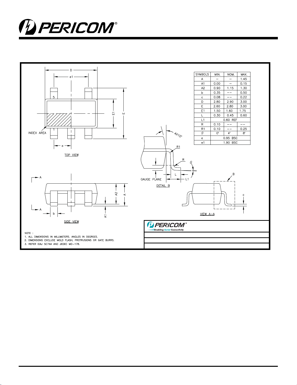
Packaging Mechanical: 6-pin SOT23 (T)
09-0002
PI5A121/PI5A122/PI5A124
Wide Bandwidth Analog Switch
DESCRIPTION: 6-pin, Small Outline Transistor Plastic Package (SOT23)
PACKAGE CODE: T (T6)
DOCUMENT CONTROL #: PD-1912
09-0131
Note:
• For latest package info, please check: http://www.pericom.com/products/packaging/mechanicals.php
Ordering Information
Ordeing Code Packaging Code Package Type Top Marking
PI5A121TX T 5-pin, 65-mil wide SOT-23 ZV
PI5A121TEX T Pb-free & Green, 5-pin, 65-mil wide SOT23
PI5A121CEX C Pb-free & Green, 5-pin, 50-mil wide SOT23
PI5A122TEX T Pb-free & Green, 5-pin, 65-mil wide SOT23
PI5A122CEX C Pb-free & Green, 5-pin, 50-mil wide SOT23
PI5A124TX T 6-pin, 65-mil wide SOT23 ZT
PI5A124TEX T Pb-free & Green, 6-pin, 65-mil wide SOT23
Notes:
• Thermal characteristics can be found on the company web site at www.pericom.com/packaging/
• E = Pb-free and Green
• Adding an X sufx = Tape/Reel
Pericom Semiconductor Corporation • 1-800-435-2336 • www.pericom.com
DATE: 10/19/09
REVISION: C
ZV
ZV
ZU
ZU
ZT
9
PS8203H 10/23/09

 Loading...