

12345678901234567890123456789012123456789012345678901234567890121234567890123456789012345678901212345678901234567890123456789012123456789012
1
2
12345678901234567890123456789012123456789012345678901234567890121234567890123456789012345678901212345678901234567890123456789012123456789012
查询PI3C16215供应商
234567890123456789012345678901212345678901234567890123456789012123456789012345678901234567890121234567890123456789012345678901212345678901
PI3C16215
3.3V, 2-Port, 20-Bit Bus Switch
with Precharged Outputs
for Live Insertion
Product Features
Near zero propagation delay
5-ohm switch connection between two ports
High Bandwidth (>200 MHz)
Rail-to-Rail 3.3V Switching
Outputs are precharged by bias voltage to
minimize signal distortion during live insertion
5V I/O Tolerant
Package options:
48-pin 150 mil wide plastic BQSOP (B)
48-pin 240 mil wide plastic TSSOP (A)
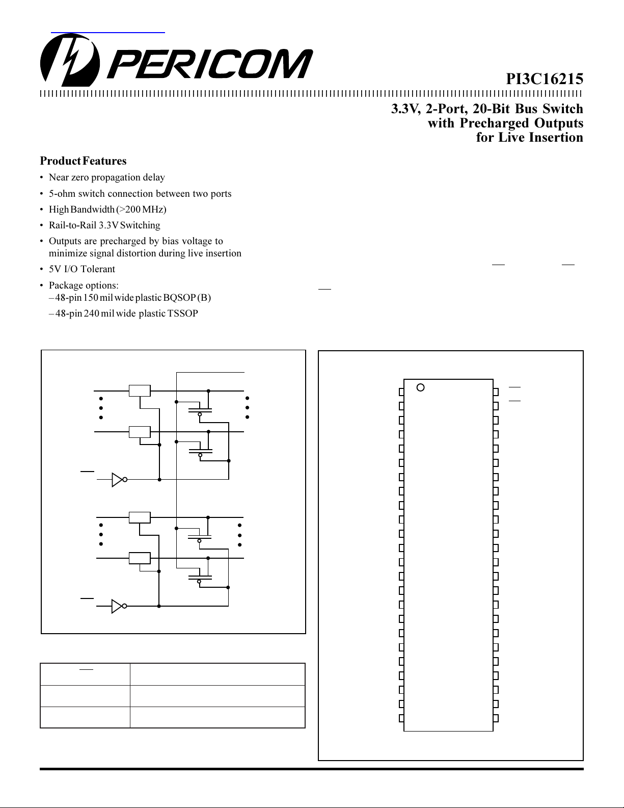
Logic Diagram
1
1
1
1
2
A
A
OE
OE
10
2
1
12
48
13
24
47
SW
SW
SW
SW
46
36
35
25
Truth Table
EOnoitcnuF
LtropB=tropA
HVSAIB=tropA,Z=tropA
Note:
1. H= High Voltage Level 2. L= Low Voltage Level
BIASV
1B1
1
B10
2B1
2
B10
Product Description
Pericom Semiconductors PI3C series of logic circuits are produced
using the Companys advanced submicron CMOS technology,
achieving industry leading performance.
The PI3C16215 is a 20-bit bus switch with low ON-State resistance.
The bus switch creates no additional propagation delay. To minimize
live-insertion noise, the device also precharges the B port to a userselectable bias voltage (BIASV).
The switch is turned on by a single enable (OE) input. When OE is
LOW, the switch is on and port A is connnected to port B. When
OE is HIGH, the switch between port A and port B is open and
the B port is precharged to BIASV through the equivalent of a
10k-ohm resistor.
Product Pin Configuration
BIASV
1A1
1A2
1A3
1A4
1A5
1A6
GND
1A7
1A8
1A9
1A10
2A1
2A2
V
CC
2A3
GND
2A4
2A5
2A6
2A7
2A8
2A9
2A10
1
2
3
4
5
6
7
8
9
10
11
12
13
14
15
16
17
18
19
20
21
22
23
24
48-Pin
A,B
48
47
46
45
44
43
42
41
40
39
38
37
36
35
34
33
32
31
30
29
28
27
26
25
1OE
2OE
1B1
1B2
1B3
1B4
1B5
GND
1B6
1B7
1B8
1B9
1B10
2B1
2B2
2B3
GND
2B4
2B5
2B6
2B7
2B8
2B9
2B10
1
PS8409D 03/19/01

PI3C16215
3.3V, 2-Port, 20-Bit Bus Switch with
Precharged Outputs for Live Insertion
Absolute Maximum Ratings Over Free-Air Temperature Range
(Above which the useful life may be impaired. For user guidelines, not tested.)
Storage Temperature...................................... 65°C to +150°C
Supply Voltage Range .......................................... 0.5V to 4.6V
DC Input Voltage
Input Clamp Current, IIK (V1< 0) ..................................... 50mA
DC Output Current .......................................................... 120mA
Power Dissipation
Notes:
1. The input and output negative-voltage ratings may be exceeded if the input and output clamp-current ratings are observed.
2. The maximum package power dissipation is calculated using a junction temperatue of 150°C and a board trace length of 750 mils.
(1)
............................................ 0.5V to +5.5V
(2)
..........................................................0.5W
Note:
Stresses greater than those listed under MAXIMUM
RATINGS may cause permanent damage to the device. This
is a stress rating only and functional operation of the device
at these or any other conditions above those indicated in
the operational sections of this specification is not implied.
Exposure to absolute maximum rating conditions for
extended periods may affect reliability.
*
Recommended Operating Conditions
.niM.xaMstinU
V
CC
VSAIBegatlovylppuS3.1V
V
HI
V
LI
T
A
egatlovylppuS0.33.3
egatlovtupnilevel-hgiH2
egatlovtupnilevel-woL8.0
erutarepmetria-eerfgnitarepO0458C°
CC
V
Electrical Characteristics (Over Recommended Operating Free-Air Temperature Range)
1
2
3
4
5
6
7
8
sretemaraPnoitpircseDsnoitidnoCtseT.niMpyT .
V
KI
I
I
I
O
I
CC
∆I
CC
C
NI
C
FFO
*
R
NO
Notes:
* Measured by the voltage drop between the A and B terminals at the indicated current through the switch.
On-state resistance is determined by the lower of the voltages of the two (A or B) terminals.
This is the increase in supply current for control input.
All typical values are at VCC = 3.3V, TA = 25°C.
egatloVedoiDpmalCV
tnerruCtupnIV
tnerruCtuptuOVCCV,V4.2=VSAIB,V0.3=
tnerruCylppuSrewoPtnecseiuQV
tupnIreptnerruCylppuSrewoP
ecnaticapaCtupnIV
ecnaticapaCB/AV
ecnatsiseRnohctiwSV
CC
CC
CC
V
CC
CC
CC
CC
I,V0.3=
,V6.3=VNIV=
I,V6.3=
O
,V6.3=V7.2tatupnienO
tarehtOVCCDNGro
V0=5.3
,V0=ffOhctiwS0.5
V0.3=
81=mA 37.02.1V
NI
DNGro5±
O
CC
I,0=
46=Am55.8
NI
I,V4.2=
NI
I,V4.2=
NI
V
V
V
CC
,0=VNIV=
NI
NI
NI
0=52.0Am
DNGro062058
03=Am0.851
51=Am0.851
.xaMstinU
9
µA
10
µA
11
5.2Am
12
Fp
13
Ω
14
15
2
PS8409D 03/19/01

PI3C16215
3.3V, 2-Port, 20-Bit Bus Switch with
Precharged Outputs for Live Insertion
Switching Characteristics (Over Recommended Operating Free-air Temperature Range, C
)tupnI(morF)tuptuO(oT
BroAAroB52.0
)1(
t
DP
t
HZP
retemaraPsnoitidnoCtseT
DNG=VSAIB
= 50pF)
L
.niM.xaMstinU
5.15.6
NOBroA
t
LZP
t
ZHP
V3=VSAIB5.15.6
DNG=VSAIB
5.15.5
sn
NOBroA
t
ZLP
V3=VSAIB5.15.5
Note:
1. This parameter is warranted but not production tested. The propagation delay is based on the RC time constant of the typical on
state resistance of the switch and a load capacitance of 50pF, when driven by an ideal voltage source (zero output impedance).
Parameter Measurements
tseT1S
t
DP
t
t/
ZLP
LZP
t/
t
ZHP
HZP
nepO
V6
DNG
From Output
Under Test
CL = 50pF
(See note 1)
500
Ohm
500
Ohm
S1
6V
Open
GND
1
2
3
4
5
6
7
LOAD CIRCUIT
VOLTAGE WAVEFORMS
PROPAGATION DELAY TIMES
Output
Control
(Low Level
Enabling)
Output
Waveform 1
S1 at 6V
(see Note 2)
Output
Waveform 2
S1 at Open
(see Note 2)
1.5V
t
PZL
t
PZH
VOLTAGE WAVEFORMS
ENABLE AND DISABLE TIMES
1.5V
1.5V
t
PLZ
t
PHZ
1.5V
V
OL
V
+0.3V
OH
-0.3V
3V
0V
3.5V
V
V
0V
OL
OH
Notes:
1. CL includes probe and jig capacitance.
2. Waveform 1 is for an output with internal conditions such that the output is LOW except when disabled by the output control.
Waveform 2 is for an output with internal conditions such that the output is HIGH except when disabled by the output control.
3. All input pulses are supplied by generators having the following characteristics: PRR<10MHz, Z
= 50Ω, tR ≤ 2.5ns, tF ≤ 2.5ns.
O
4. The outputs are measured one at a time with one transition per measurement.
5. t
6. t
7. t
PLZ
PZL
PLH
and t
and t
and t
are the same as t
PHZ
are the same as tEN.
PZH
are the same as tPD.
PHL
DIS
.
8
9
10
11
12
13
14
15
3
PS8409D 03/19/01
PI3C16215
3.3V, 2-Port, 20-Bit Bus Switch with
Precharged Outputs for Live Insertion
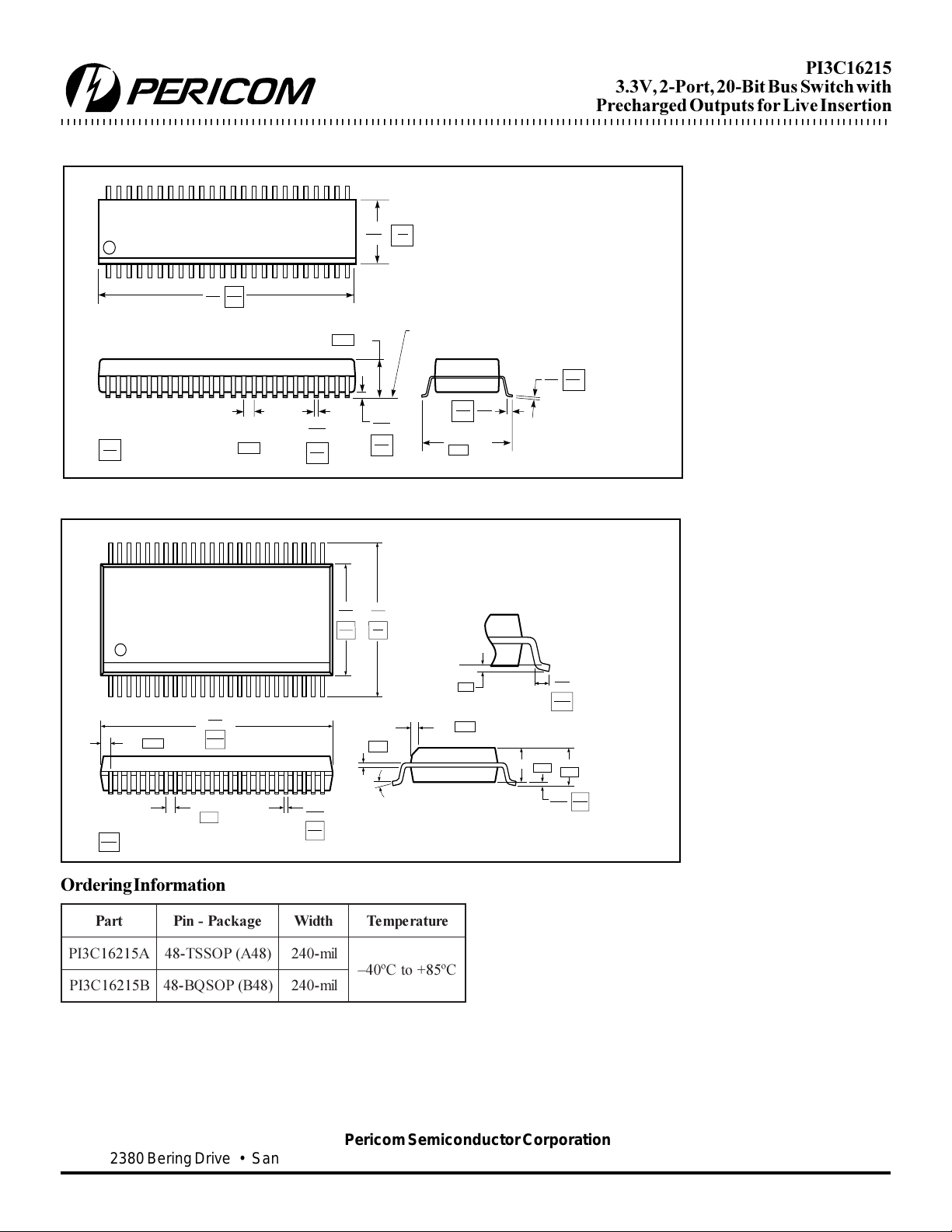
48-Pin TSSOP (A) Package
48
1
X.XX
DENOTES DIMENSIONS
X.XX
IN MILLIMETERS
.488
12.4
.496
12.6
.0197
BSC
0.50 0.17
48-Pin BQSOP (B) Package
48
.007
.010
0.27
.047
1.20 Max
.236
.244
.002
.006
0.05
0.15
6.0
6.2
SEATING PLANE
.319
8.1
0.45
0.75
BSC
.018
.030
.004
.008
0.09
0.20
1
2
3
4
5
6
1
.014
0.356
X.XX
DENOTES DIMENSIONS
X.XX
IN MILLIMETERS
REF
.386
.394
9.80
10.00
.0157 BSC
0.40
Ordering Information
traPegakcaP-niPhtdiWerutarepmeT
A51261C3IP)84A(POSST-84lim-042
B51261C3IP)84B(POSQB-84lim-042
.0051
.009
0.13
0.23
.150
.157
3.80
4.00
.228
.244
5.80
6.20
.008 0.20
Nom
5˚
Gauge Plane
.010
.015 0.381
Cº58+otCº04
.020
.063
Nom
1.60
.002
.009
.029
0.50
0.75
.079
2.0
0.05
0.25
Max
BSC
0.25
x 45˚
Applications Information
Logic Inputs
The logic control inputs can be driven up to +3.6V regardless of the
supply voltage. For example, given a +3.3V supply, IN may be driven
low to 0V and high to 3.6V. Driving IN Rail-to-Rail® minimizes power
consumption.
Power-Supply Sequencing
Proper power-supply sequencing is recommended for all CMOS
devices. Always apply VCC before applying V
input/output or control pins.
Rail-to-Rail is a registered trademark of Nippon Motorola, Ltd
and signals to
BIAS
7
8
9
10
11
12
13
14
15
Pericom Semiconductor Corporation
2380 Bering Drive • San Jose, CA 95131 • 1-800-435-2336 • Fax (408) 435-1100 • http://www.pericom.com
4
PS8409D 03/19/01

Copyright © Each Manufacturing Company.
All Datasheets cannot be modified without permission.
This datasheet has been download from :
www.AllDataSheet.com
100% Free DataSheet Search Site.
Free Download.
No Register.
Fast Search System.
www.AllDataSheet.com
 Loading...