


12345678901234567890123456789012123456789012345678901234567890121234567890123456789012345678901212345678901234567890123456789012123456789012
1
2
12345678901234567890123456789012123456789012345678901234567890121234567890123456789012345678901212345678901234567890123456789012123456789012
PI74FCT373T
PI74FCT573T
234567890123456789012345678901212345678901234567890123456789012123456789012345678901234567890121234567890123456789012345678901212345678901
Octal Transparent Latches
Fast CMOS Octal
Transparent Latches
Features:
• PI74FCT373/573T are pin compatible with bipolar FAST™
Series at a higher speed and lower power consumption
• TTL input and output levels
• Low ground bounce outputs
• Extremely low static power
• Hysteresis on all inputs
• Industrial operating temperature range: –40°C to +85°C
• Device models available upon request
• Packaging:
– 20-pin TSSOP (L)
– 20-pin SSOP (H)
– 20-pin QSOP (Q)
– 20-pin SOIC (S)
Block Diagram
D0
D
D1
D
O
G
D2
D
O
G
D3
O
G
Description:
Pericom Semiconductor’s PI74FCT373T and PI74FCT 573T are
8-bit wide octal transparent latches designed with 3-state outputs
and are intended for bus oriented applications. When Latch Enable
(LE) is HIGH, the flip-flops appear transparent to the data. The data
that meets the set-up time when LE is LOW is latched. When OE is
HIGH, the bus output is in the high impedance state.
D4
D
O
G
D
D5
D
O
G
D6
D
O
G
D7
D
O
G
O
G
LE
OE
O0
O1
O2
O3
1
O4
O5
O6
O7
PS2015B 10/06/04

PI74FCT373T
PI74FCT573T
OCTAL TRANSPARENT LATCHES
PI74FCT373 Pin Configuration
1
OE
O
0
2
D
0
3
4
5
6
7
8
9
10
20-PIN
L20
P20
Q20
S20
D
O
O
D
D
O
GND
1
1
2
2
3
3
PI74FCT573 Pin Configuration
1
OE
0
D
2
3
4
5
6
7
8
9
10
20-PIN
L20
P20
Q20
S20
D
D
D
D
D
D
D
GND
1
2
3
4
5
6
7
20
19
18
17
16
15
14
13
12
11
20
19
18
17
16
15
14
13
12
11
Vcc
O
7
D
7
D
6
O
6
O
5
D
5
D
4
O
4
LE
Vcc
O
0
O
1
O
2
O
3
O
4
O
5
O
6
O
7
LE
Pin Description
Pin Name Description
OE Output Enable Input (Active LOW)
LE Latch Enable Input (Active HIGH)
D0-D7 Data Inputs
O0-O7 3-State Outputs
O0-O7 Complementary 3-State Outputs
GND Ground
VCC Power
Truth Table
DN LE OE ON
HHLH
LHLL
XXHZ
1. H = High Voltage Level
L = Low Voltage Level
X = Don’t Care
Z = High Impedance
(1)
Inputs Outputs
2
PS2015B 10/06/04

PI74FCT373T
12345678901234567890123456789012123456789012345678901234567890121234567890123456789012345678901212345678901234567890123456789012123456789012
12345678901234567890123456789012123456789012345678901234567890121234567890123456789012345678901212345678901234567890123456789012123456789012
PI74FCT573T
OCTAL TRANSPARENT LATCHES
Maximum Ratings
(Above which the useful life may be impaired. For user guidelines, not tested.)
Storage Temperature ................................................................. –65°C to +150°C
Ambient Temperature with Power Applied ................................. -40°C to +85°C
Supply Voltage to Ground Potential (Inputs & Vcc Only) .......... –0.5V to +7.0V
Supply Voltage to Ground Potential (Outputs & D/O Only) ....... –0.5V to +7.0V
DC Input Voltage ......................................................................... –0.5V to +7.0V
DC Output Current ................................................................................... 120 mA
Note:
Stresses greater than those listed under MAXIMUM RATINGS may cause permanent damage to
the device. This is a stress rating only and functional
operation of the device at these or any other
conditions above those indicated in the operational
sections of this specification is not implied.
Exposure to absolute maximum rating conditions for
extended periods may affect reliability.
Power Dissipation ......................................................................................... 0.5W
DC Electrical Characteristics (Over the Operating Range, TA = –40°C to +85°C, VCC = 5.0V ± 5%)
Parameters Description Test Conditions
(1)
Min. Typ
VOH Output HIGH Voltage VCC = Min., VIN = VIH or VIL IOH = –15.0 mA 2.4 3.0 V
VOL Output LOW Current VCC = Min., VIN = VIH or VIL IOL = 64 mA 0.3 0.55 V
(2)
Max. Units
VOL Output LOW Current VCC = Min., VIN = VIH or VIL IOL = 12 mA (25Ω Series) 0.3 0.50 V
VIH Input HIGH Voltage Guaranteed Logic HIGH Level 2.0 V
VIL Input LOW Voltage Guaranteed Logic LOW Level 0.8 V
IIH Input HIGH Current VCC = Max. VIN = VCC 1µA
IIL Input LOW Current VCC = Max. VIN = GND – 1 µA
IOZH High Impedance VCC = MAX.VOUT = 2.7V 1 µA
IOZL Output Current VOUT = 0.5V –1 µA
VIK Clamp Diode Voltage VCC = Min., IIN = –18 mA –0.7 –1.2 V
IOFF Power Down Disable VCC = GND, V OUT = 4.5V — — 10 0 µA
IOS Short Circuit Current VCC = Max.
(3)
, VOUT = GND –60 –120 mA
VH Input Hysteresis 200 mV
Capacitance (TA = 25°C, f = 1 MHz)
Parameters
CIN Input Capacitance VIN = 0V 6 10 pF
COUT Output Capacitance VOUT = 0V 8 12 pF
(4)
Description Test Conditions Typ Max. Units
Notes:
1. For Max. or Min. conditions, use appropriate value specified under Electrical Characteristics for the applicable device type.
2. Typical values are at Vcc = 5.0V, +25°C ambient and maximum loading.
3. Not more than one output should be shorted at one time. Duration of the test should not exceed one second.
4. This parameter is determined by device characterization but is not production tested.
3
PS2015B 10/06/04
PI74FCT373T
PI74FCT573T
OCTAL TRANSPARENT LATCHES
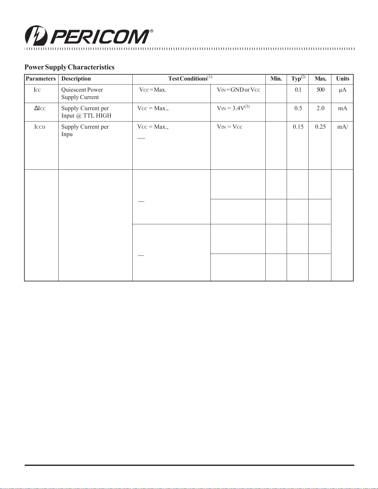
Power Supply Characteristics
Parameters Description Test Conditions
(1)
Min. Typ
ICC Quiescent Power VCC = Max. VIN = GND or VCC 0.1 500 µA
Supply Current
∆ICC Supply Current per VCC = Max., VIN = 3.4V
(3)
Input @ TTL HIGH
(2)
Max. Units
0.5 2.0 mA
ICCD Supply Current per VCC = Max., VIN = VCC 0.15 0.25 mA/
Input per MHz
(4)
Outputs Open VIN = GND MHz
OE = GND
LE = VCC
One Bit Toggling
50% Duty Cycle
IC Total Power Supply VCC = Max., VIN = VCC 1.5 3.0
Current
(6)
Outputs Open VIN = GND
(5)
fI = 10 MHZ
50% Duty Cycle
OE = GND VIN = 3.4V 1.8 4.5
(5)
LE = VCC VIN = GND
One Bit Toggling
VCC = Max., VIN = VCC 3.0 6.0
(5)
Outputs Open VIN = GND
fI = 2.5 MHZ
50% Duty Cycle
OE = GND VIN = 3.4V 5.0 14.0
LE = VCC VIN = GND
Eight Bits Toggling
Notes:
1. For conditions shown as Max. or Min., use appropriate value specified under Electrical Characteristics for the applicable device.
2. Typical values are at Vcc = 5.0V, +25°C ambient.
3. Per TTL driven input (V
4. This parameter is not directly testable, but is derived for use in Total Power Supply Calculations.
5. Values for these conditions are examples of the Icc formula. These limits are guaranteed but not tested.
C =IQUIESCENT + IINPUTS + IDYNAMIC
6. I
IC = ICC + ∆ICC DHNT + ICCD (fCP/2 + fINi)
CC = Quiescent Current
I
∆I
CC = Power Supply Current for a TTL High Input (VIN = 3.4V)
H = Duty Cycle for TTL Inputs High
D
T = Number of TTL Inputs at DH
N
ICCD = Dynamic Current Caused by an Input Transition Pair (HLH or LHL)
CP = Clock Frequency for Register Devices (Zero for Non-Register Devices)
f
I = Input Frequency
f
N
I = Number of Inputs at fI
All currents are in milliamps and all frequencies are in megahertz.
IN = 3.4V); all other inputs at Vcc or GND.
mA
(5)
4
PS2015B 10/06/04

12345678901234567890123456789012123456789012345678901234567890121234567890123456789012345678901212345678901234567890123456789012123456789012
12345678901234567890123456789012123456789012345678901234567890121234567890123456789012345678901212345678901234567890123456789012123456789012
PI74FCT373T Switching Characteristics over Operating Range
373T 373AT 373CT 373DT
Com. Com. Com. Com.
Parameters Description Conditions
t
PLH
t
PHL
t
PLH
t
PHL
t
PZH
t
PZL
t
PHZ
t
PLZ
t
SU
t
H
t
W
Propagation Delay CL = 5 0 p F 1.5 8.0 1.5 5.2 1.5 4.2 1.5 3.8 ns
DN to O
N
RL = 500
Propagation Delay 2.0 13.0 2.0 8.5 2.0 5.5 1.5 4.9 ns
LE to O
N
Output Enable Time 1.5 12.0 1.5 6.5 1.5 5.5 1.5 5.5 ns
OE to O
N
Output Disable Time
OE to O
N
(3)
Setup Time HIGH or 2.0 — 2.0 — 2.0 — 2.0 — ns
LOW, D
N
to LE
Hold Time HIGH or 1.5 — 1.5 — 1.5 — 1.5 — ns
LOW, D
N
to LE
LE Pulse Width
(3)
HIGH
(1)
Min Max Min Max Min Max Min Max Unit
Ω
1.5 7.5 1.5 5.5 1.5 5.0 1.5 5.0 ns
6.0 — 5.0 — 5.0 — 4.0 — ns
PI74FCT373T
PI74FCT573T
OCTAL TRANSPARENT LATCHES
PI74FCT573T Switching Characteristics over Operating Range
573T 573AT 573CT 573DT
Com. Com. Com. Com.
Parameters Description Conditions
t
PLH
t
PHL
t
PLH
t
PHL
t
PZH
t
PZL
t
PHZ
t
PLZ
t
SU
t
H
t
W
Propagation Delay CL = 5 0 p F 1.5 8.0 1.5 5.2 1.5 4.2 1.5 3.8 ns
DN to O
N
RL = 500
Propagation Delay 2.0 12.0 2.0 8.5 2.0 5.5 2.0 4.9 ns
LE to O
N
Output Enable Time 1.5 9.5 1.5 6.5 1.5 5.5 1.5 5.5 ns
OE to O
N
Output Disable Time
OE to O
N
(3)
Setup Time HIGH or 2.0 — 2.0 — 2.0 — 1.5 — ns
LOW, D
N
to LE
Hold Time HIGH or 1.5 — 1.5 — 1.5 — 1.0 — ns
LOW, D
N
to LE
LE Pulse Width
(3)
HIGH
Notes:
1. See test circuit and wave forms.
2. Minimum limits are guaranteed but not tested on Propagation Delays.
3. This parameter guaranteed but not production tested.
(1)
Min Max Min Max Min Max Min Max Unit
Ω
1.5 6.5 1.5 5.5 1.5 5.0 1.5 5.0 ns
6.0 — 5.0 — 5.0 — 3.0 — ns
5
PS2015B 10/06/04
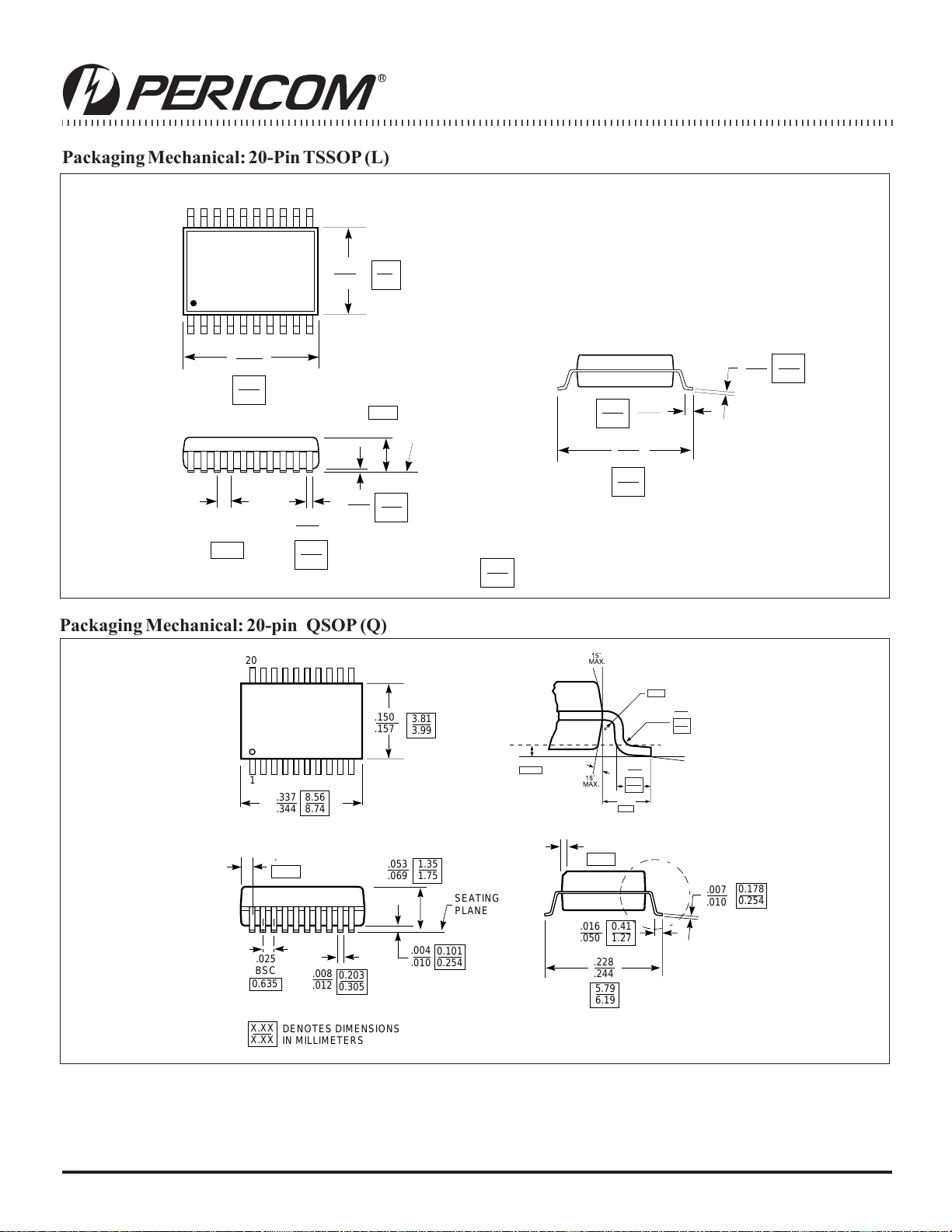
Packaging Mechanical: 20-Pin TSSOP (L)
20
.169
4.3
.177
4.5
PI74FCT373T
PI74FCT573T
OCTAL TRANSPARENT LATCHES
1
.252
.260
6.4
6.6
.047
1.20
Max
.002
.0256
BSC
0.65
.007
.012
0.19
0.30
.006
Packaging Mechanical: 20-pin QSOP (Q)
20
.150
.157
1
8.56
.337
.344
8.74
0.05
0.15
SEATING
PLANE
3.81
3.99
0.45
0.75
X.XX
DENOTES CONTROLLING
X.XX
DIMENSIONS IN MILLIMETERS
Guage Plane
.010
0.254
Detail A
.238
.269
6.1
6.7
.041
1.04
REF
.016
.035
0.41
0.89
.018
.030
.008
0.20
MIN.
0.09
.004
0.20
.008
.008
.013
0.20
0.33
0˚-6˚
.058
REF
1.47
.025
BSC
0.635
X.XX
X.XX
.008
.012
DENOTES DIMENSIONS
IN MILLIMETERS
0.203
0.305
.053
.069
1.35
1.75
.004
.010
0.101
0.254
SEATING
PLANE
6
.015 x 45˚
0.38
.016
.050
.228
.244
5.79
6.19
0.41
1.27
Detail A
.007
.010
0.178
0.254
PS2015B 10/06/04

12345678901234567890123456789012123456789012345678901234567890121234567890123456789012345678901212345678901234567890123456789012123456789012
12345678901234567890123456789012123456789012345678901234567890121234567890123456789012345678901212345678901234567890123456789012123456789012
Packaging Mechanical: 20-Pin SSOP (H)
20
.197
.220
5.00
5.60
PI74FCT373T
PI74FCT573T
OCTAL TRANSPARENT LATCHES
X.XX
X.XX
1
.272
.295
6.90
7.50
.0256
BSC
0.65
DENOTES DIMENSIONS
IN MILLIMETERS
.0098
Max.
0.25
.078
2.00
Packaging Mechanical: 20-pin SOIC (S)
20
1
.496
12.60
.511
12.99
.020
0.508
.030
0.762
REF
.0926
.1043
Max
.2914
.2992
.002
0.050
2.35
2.65
Min
7.40
7.60
SEATING
PLANE
SEATING
PLANE
0-8˚
.010
.029
0.41
1.27
.394
.419
10.00
10.65
0.55
0.95
.291
.322
7.40
8.20
.022
.037
0.254
0.737
.016
.050
x 45˚
.0091
.0125
.004
.009
0.23
0.32
0.09
0.25
0.10
.0040
0.30
.050
BSC
1.27
.013
.020
0.33
0.51
.0118
X.XX
DENOTES CONTROLLING
X.XX
DIMENSIONS IN MILLIMETERS
7
PS2015B 10/06/04

OCTAL TRANSPARENT LATCHES
PI74FCT373T Ordering Information
Ordering Code Package Code Speed Grade Package Type
PI74FCT373TL L Blank 20-pin TSSOP
PI74FCT373TQ Q Blank 20-pin QSOP
PI74FCT373TS S Blank 20-pin SOIC
PI74FCT373ATH H A 20-pin SSOP
PI74FCT373ATL L A 20-pin TSSOP
PI74FCT373ATS S A 20-pin SOIC
PI74FCT373ATQ Q A 20-pin QSOP
PI74FCT373CTH H C 20-pin SSOP
PI74FCT373CTL L C 20-pin TSSOP
PI74FCT373CTS S C 20-pin SOIC
PI74FCT373CTQ Q C 20-pin QSOP
PI74FCT373DTH H D 20-pin SSOP
PI74FCT373DTL L D 20-pin TSSOP
PI74FCT373DTQ Q D 20-pin QSOP
PI74FCT373T
PI74FCT573T
PI74FCT573T Ordering Information
Ordering Code Package Code Speed Grade Package Type
PI74FCT573TQ Q Blank 20-pin QSOP
PI74FCT573TS S Blank 20-pin SOIC
PI74FCT573ATH H A 20-pin SSOP
PI74FCT573ATL L A 20-pin TSSOP
PI74FCT573ATS S A 20-pin SOIC
PI74FCT573ATQ Q A 20-pin QSOP
PI74FCT573CTH H C 20-pin SSOP
PI74FCT573CTL L C 20-pin TSSOP
PI74FCT573CTS S C 20-pin SOIC
PI74FCT573CTQ Q C 20-pin QSOP
PI74FCT573DTQ Q D 20-pin QSOP
Notes:
1. Thermal characteristics can be found on the company web site at www.pericom.com/packaging/
Pericom Semiconductor Corporation • 1-800-435-2336 • www.pericom.com
8
PS2015B 10/06/04

WWW.ALLDATASHEET.COM
Copyright © Each Manufacturing Company.
All Datasheets cannot be modified without permission.
This datasheet has been download from :
www.AllDataSheet.com
100% Free DataSheet Search Site.
Free Download.
No Register.
Fast Search System.
www.AllDataSheet.com
 Loading...