

Page 1

Document Number 126A0190
Performance
Computer
USER’S MANUAL
PT-VME161
Extensible Single Board Computer/Controller
A Performance Technologies Company
315 Science Parkwa y
Rochester, New York USA 14620
Page 2

Rev ECN Pages Affected Date Approvals
10 - All 09/20/94
REVISION CONTROL
When reviewing this document please note any issues that you may have with the document (errors,
points of confusion, grammar or spelling mistakes, etc.) and contact Technical Publications at (716) 2560200 or [email protected]. All comments, su ggestions, and criticisms are welcome.
Copyright Notice
© 1993-1994 by Performance Computer, a Performance Technologies Company. -- Printed in USA.
315 Science Parkway, Rochester, New York 14620
Trademarks
Microware
PTbug
All other brands or names are trademarks of their respective holders.
All rights reserved. This document is the sole property of Performance C omputer.
OS-9
and
is a trademark of Performance Computer.
are trademarks of Microware Systems Corporation.
Page 3

NOTICE
This document presents information for users of the Performance Computer Models PT-VME161 Extensible Single Board Computer/Controller.
Although the information contained within this document is considered accurate and characteristic of the
subject product, Performance Computer reserves the right to make changes to this document and any products described herein to improve reliability, function, or design. Performance Computer does not assume
any liability arising out of the application or use of any product or circuit described herein.
No part of this document may be copied or reproduced in any form or by any means without the prior
permission of Performance Computer.
WARNING
THIS EQUIPMENT GENERATES, USES, AND CAN RADIATE RADIO FREQUENCY ENERGY
AND, IF NOT INSTALLED AND USED IN ACCORDANCE WITH THE INSTRUCTION MANUAL,
MAY CAUSE INTERFERENCE TO RADIO COMMUNICATIONS. AS TEMPORARILY
PERMITTED BY REGULATION, IT HAS NOT BEEN TESTED FOR COMPLIANCE WITH THE
LIMITS FOR CLASS A COMPUTING DEVICES PURSUANT TO SUBPART J OF PART 15 OF FCC
RULES, WHICH ARE DESIGNED TO PROVIDE REASONABLE PROTECTION AGAINST SUCH
INTERFERENCE. OPERATION OF THIS EQUIPMENT IN A RESIDENTIAL AREA IS LIKELY TO
CAUSE INTERFERENCE, IN WHICH CASE THE USER, AT HIS OWN EXPENSE, WILL BE
REQUIRED TO TAKE WHATEVER MEASURES MAY BE REQUIRED TO CORRECT THE INTERFERENCE.
Page 4
Safety Information
This section is provided as a summary of the safety recommendations throughout this manual. Performance Computer (PCC) recommends that all safety precautions are followed to prevent harm to yourself
or the equipment. Please follow all warnings marked on the equipment.
Safety Precautions
• Follow all warnings and instructions marked on the equipment.
• Ensure that the voltage and frequency of your power source matches the voltage and frequency
• Never push objects of any kind through the openings in the equipment. Dangerous voltages may be
Symbols
The following symbols appear in th is document.
inscribed on the equipments electrical rating label.
present. Conductive foreign objects could produce a short circuit that could cause fire, electrical
shock, or damage your equipment.
!
CAUTION: There is risk of personal injury or equipment damage. Follow the instructions.
WARNING: Hazardous voltages are present. To reduce the risk of electric shock and dang er to personal
heath, follow the instructions.
Page 5

Performance Computer
Table of Contents
Section 1 PT-VME161 INTRODUCTION
Scope
Applicable Documents
Model Designations
Features
Family Members
Glossary and Conventions
Section 2 GETTING STARTED
Unpacking and Inspection
Hardware Configuration
............................................................................................................................. 1
............................................................................................. 2
.................................................................................................. 3
........................................................................................................................ 4
......................................................................................................... 6
PT-VME131/131E........................................................................................................ 6
PT-VME141/141E........................................................................................................ 7
PT-VME151A/151AE................................................................................................... 7
..................................................................................... 8
Glossary ...................................................................................................................... 8
Conventions............... .................................................................................................. 9
.................................................................. 11
..................................................................................... 11
......................................................................................... 12
Device Positions......................................................................................................... 12
U24 PROM/ROM/SRAM/EEPROM Socket Configuration......................................... 14
Location U24 Setup............................................................................................... 15
Location U36 Setup............................................................................................... 15
SCSI Termination....................................................................................................... 17
Disabling Termination........................................................................................... 17
Termination Power Source.................................................................................... 17
TERMPWR Overview...................................................................................... 17
DRAM Module Upgrading........................................................................................... 19
EPAK Installation........................................................................................................ 20
.............................................. 1
Board Installation
Power Considerations................................................................................................ 21
Slot Considerations.................................................................................................... 21
Backplane Insertion.................................................................................................... 21
..................................................................................................... 21
SCSI Considerations
Cabling ....................................................................................................................... 23
Example................................................................................................................ 23
Mechanical restraints............................................................................................ 24
............................................................................................... 23
Extensible Single Board Computer/Controller User’s Manual v
Page 6

Table of Contents
SCSI device grounds............................................................................................ 24
Device addresses....................................................................................................... 25
Serial Port Cabling
Example...................................................................................................................... 25
Mechanical restraints..................................................................................................26
................................................................................................... 25
Section 3 FUNCTIONAL DESCRIPTION
Microprocessor
Memory
DRAM......................................................................................................................... 28
Parity ..........................................................................................................................30
PROM/SRAM Sockets................................................................................................31
Nonvolatile SRAM and Time of Day/Calendar Clock .................................................31
Serial EEPROM.......................................................................................................... 31
......................................................................................................................... 28
DRAM Mapping..................................................................................................... 29
Sizing.................................................................................................................... 29
Checking............................................................................................................... 30
Initialization ........................................................................................................... 31
Testing .................................................................................................................. 31
Interval Timer
VMEbus Interface
SCV64........................................................................................................................ 33
VME64 Transfers.................................................................................................. 33
Transfer Modes..................................................................................................... 33
Decoupled........................................................................................................ 33
Atomic.............................................................................................................. 34
VMEbus Control Logic.......................................................................................... 34
VMEbus Slave Accesses...................................................................................... 35
SCV64 register access from the VMEbus ....................................................... 35
EPAK access from the VMEbus......................................................................35
VMEbus Master Accesses.................................................................................... 35
68060 Accesses........... ..... .... .......................................................................... 35
Read-Modify-Write............................................. ..... ..... .................................... 36
DMAC............................ ..... ................................................................................... 36
Location Monitor.................................................................................................... 37
Registers............................................................................................................... 37
Test and Diagnostics.............................................................................................37
Reset..................................................................................................................... 38
Local Bus Timer.................................... .... ..... ....................................................... 38
Watchdog Timer........................................ ..... ..... .... .............................................. 38
Tick Timer .............................................................................................................38
Register Block....................................................................................................... 39
Interrupt Handler................................................................................................... 39
......................................................................................................... 28
.............................................................................................................32
...................................................................................................... 33
........................................... 27
vi Extensible Single Board Computer/Controller User’s Manual
Page 7

Performance Compute
r
Local Level 7 Sources................ ..... ................................................................ 39
Abort............................................... ..... ..... .................................................. 39
SCSI Bus Reset......................................................................................... 40
AC Fail.......................... .... ..... ..... ................................................................ 40
System Fail................................................................................................. 40
General Purpose Local Interrupts.................................................................... 40
Location Monitor FIFO................ .... ............................................................40
SCV64 VME Event..................................................................................... 41
Timer Event................................................................................................ 41
Tick ....................................................................................................... 41
Interval.................................................................................................. 42
I/O Event.................................................................................................... 42
FAS216 Requests................................................................................. 42
EPAK Requests (-EPIRQ).................................................................... 42
EPAK Vectored Interrupt Request.............................................................. 42
DUART Interrupt Request (-INTP<5>)....................................................... 43
VMEbus Interrupts...........................................................................................43
Interrupt Acknowledgment............................................................................... 43
VMEbus Requester..........................................................................................44
System Monitor Functions...............................................................................44
Reset.......................................................................................................... 44
System Clock Driver................................................................................... 44
VMEbus Arbiter.......................................................................................... 44
IACK Daisy Chain Driver............................................................................ 45
Bus Timer................................................................................................... 45
I/O UTILITIES
..............................................................................................................45
System Control Registers........................................................................................... 45
System Control Register 1.................................................................................... 45
VMEbus Page Select.......................................................................................45
User LEDs ....................................................................................................... 46
SCSI DMA Read/Write Direction..................................................................... 46
EPAK Space Cache Enable ............................................................................ 46
VMEbus Space Cache Enable ........................................................................ 46
System Control Register 2.................................................................................... 46
Enable EPAK Access from the VMEbus.......................................................... 47
Enable Parity Error Checking.......................................................................... 47
Enable Bad Parity............................................................................................ 47
Enable Interval Timer Interrupts ...................................................................... 48
Enable Tick Timer Interrupts............................................................................ 48
Enable Bus Snooping...................................................................................... 48
System Status Registers............................................................................................ 49
System Status Register 1...................................................................................... 49
Hex Switch.......................................................................................................49
System Status Register 2...................................................................................... 49
68060 Parity Error.................. ..... ..... .... ............................................................49
Extensible Single Board Computer/Controller User’s Manual vii
Page 8

Table of Contents
SCSI DMA Parity Error....................................................................................49
DARF Parity Error............................................................................................ 49
EPAK Parity Error............................................................................................ 50
SCSI Present................................................................................................... 50
System Status Register 3...................................................................................... 50
DRAM Size...................................................................................................... 50
Parity Installed................................................................................................. 50
Interval Timer Interrupt Pending............... ..... .... .............................................. 50
DUART.................................... ..... .... ..... ..................................................................... 51
Utility Serial Ports.................................................................................................. 51
General Purpose Timer/Counter........................................................................... 51
Parallel Input Port..................................................................................................51
Clear-to-Send.................................................................................................. 51
Data-Terminal-Ready...................................................................................... 51
EPAK General Purpose Input................................. ..... .... ..... ........................... 52
Serial EEPROM Data In.................................................................................. 52
Parallel Output Port...............................................................................................52
Request-to-Send.............................................................................................. 52
Data-Set-Ready...............................................................................................52
EPAK General Purpose Output..................... .... .............................................. 52
Serial EEPROM Select.................................................................................... 52
Serial EEPROM Control.................................................................................. 52
Serial EEPROM Data Out................................................................................ 53
SCSI Controller
SCSI Bus.................................................................................................................... 54
Register Access.......................................................................................................... 54
DMA Mechanism........................................................................................................ 55
Interrupts.................................................................................................................... 55
Termination................................................................................................................. 55
EPAK Interface
.......................................................................................................... 54
...........................................................................................................57
Section 4 FUNCTIONAL SUMMARY
Memory Map
Default VMEbus Slave Addressing............................................................................. 60
161 System Registers
System Control Register 1.......................................................................................... 61
System Control Register 2.......................................................................................... 63
System Status Register 1........................................................................................... 64
System Status Register 2........................................................................................... 65
System Status Register 3........................................................................................... 66
SCSI Memory Address Register................................................................................. 67
Jumper List (Defaults)
...............................................................................................................59
.............................................................................................. 61
............................................................................................. 67
....................................................59
viii Extensible Single Board Computer/Controller User’s Manual
Page 9

Performance Compute
r
Interrupt Control
Register Maps
SCV64........................................................................................................................ 69
DS1643 Nonvolatile Timekeeping RAM.....................................................................71
82C54 Interval Timer.................................................................................................. 71
EMULEX FAS216 SCSI Controller............................................................................. 72
68681 DUART.............................. .... ..... ..................................................................... 72
Controls and Indicators
Rotary Switch............................................................................................................. 73
“RUN” Indicator........................................................................................................... 74
“FAULT” Indicator....................................................................................................... 74
“VME” Indicator........................................................................................................... 74
RESET Switch............................................................................................................ 74
ABORT Switch............................................................................................................ 74
User Programmable LEDs.......................................................................................... 74
........................................................................................................ 68
............................................................................................................69
.......................................................................................... 73
Section 5 CONNECTOR PINOUTS
Utility Serial Port Pin Assignments
VMEbus Pin Assignments
..................................................................................... 76
.................................................................... 75
......................................................... 75
EPAK Connectors
DRAM Module
..................................................................................................... 78
............................................................................................................79
Section 6 MECHANICAL AND ENVIRONMENTAL
Power Requirements
Ambient Temperature
Humidity
Vibration
....................................................................................................................... 81
....................................................................................................................... 81
Mechanical Shock
Physical Dimensions
Section 7 APPENDICES
Product Warranty
Product Return Procedure
Product Support
Installation Notes
EEPROM Usage
PTbug......................................................................................................................... 87
OS-9........................................................................................................................... 88
........................... .............................................................................. 87
............................................................................................... 81
.............................................................................................. 81
..................................................................................................... 82
.......................... ..................................................................... 82
..................................................................................83
.................................................................................... 84
........................................................................................................ 85
...................................................................................................... 86
................... 81
83
Extensible Single Board Computer/Controller User’s Manual ix
Page 10

Table of Contents
The differences between the PT-VME161 and the VME151
SCV64........................................................................................................................ 90
Differences:........................................................................................................... 90
68060 Versus 68040.......... ..... ................................................................................... 91
The differences between the PT-VME151A and the VME151
Renamed Registers....................................................................................................92
New Devices...............................................................................................................92
DRAM Sizing.............................................................................................................. 92
SRAM Access............................................................................................................. 93
PT-VME151A Differences From VME131/141
DARF64 uses 68040 mode........................................................................................ 94
SCSI Controller differences........................................................................................94
Effects of 68040 vs. 68030......................................................................................... 94
Cacheability and Serialization............................................................................... 94
68040 Cache Control Registers............................................................................ 95
68040 Cache Clearing................ .......................................................................... 96
68040 Exception Processing............ ..................................................................... 96
PT-VME151A Control Register Differences......................................... .... ..... ............. 96
SCV64 Overview
Functional Description................................................................................................ 98
BI-mode................................................................................................................. 98
Location Monitor.................................................................................................... 99
VMEbus Master Memory Map............................................................................... 99
Master VMEbus Accesses................................................................................... 101
Slave VMEbus Accesses.......................... ..... ..... ................................................. 102
........................................................................................................ 98
................................................. 94
.......................90
.................... 92
AVICS Application Notes
Local Interrupts.......................................................................................................... 104
Example:................................. ............................................................................. 104
Setting Up the Master Bus Memory Map................................................................... 105
Example:.............................................................................................................. 105
Setting Up A24/A32 Slave Images on the Bus.......................................................... 105
Example A:........................................................................................................... 106
Example B:........................................................................................................... 107
Generating VMEbus Interrupts.................................................................................. 108
Example:.............................................................................................................. 108
Receiving VMEbus Interrupts....................................................................................108
Example:.............................................................................................................. 108
Initiating a DMA Transfer...........................................................................................109
Example:.............................................................................................................. 109
...................................................................................... 104
VMEbus Address Modifiers
Section 8 SCHEMATICS
..................................................................................111
................................................................................123
x Extensible Single Board Computer/Controller User’s Manual
Page 11

Performance Computer
List of Figures
Figure 1: PT-VME161 Device Positions................................................................................ 12
Figure 2: EPROM/ROM/SRAM/EEPROM Device Orientation.............................................. 14
Figure 3: K4 and K10Jumpers............................................................................................... 15
Figure 4: K3 and K11 Jumpers.............................................................................................. 15
Figure 5: U24 and U36 Jumper Settings............................................................................... 16
Figure 6: SCSI Components.................................................................................................17
Figure 7: PT-VME161 Front Panel........................................................................................ 22
Figure 8: Example SCSI Cable............................................................................................. 24
Figure 9: Example Serial port Cable..................................................................................... 26
Figure 10: Block Diagram...................................................................................................... 27
Figure 11: Interval Timer Block Diagram............................................................................... 32
Figure 12: Timer Block Diagram............................................................................................41
Figure 13: PT-VME161 Front Panel Controls and Indicators................................................ 73
Figure 14: SCV64 Memory Map...........................................................................................100
Extensible Single Board Computer/Controller User’s Manual xi
Page 12

List of Figures
xii Extensible Single Board Computer/Controller User’s Manual
Page 13

Performance Computer
List of Tables
Table 1: EPAK Caching Options...........................................................................................46
Table 2: Memory Map........................................................................................................... 59
Table 3: Default VMEbus A24 Memory Map......................................................................... 60
Table 4: Default VMEbus A32 Memory Map......................................................................... 60
Table 5: Interrupt Request Summary.................................................................................... 68
Table 6: SCV64 Register Map............................................................................................... 69
Table 7: DS1643 Nonvolatile Timekeeping RAM Registers................................ ..... ..... .... ....71
Table 8: 82C54 Interval Timer Registers................... ............................................................71
Table 9: EMULEX FAS216 SCSI Controller Register Map................................................... 72
Table 10: Motorola 68681 DUART Register Map........... ..... .................................................. 72
Table 11: Utility Serial Port Pin Assignments........................................................................ 75
Table 12: VMEbus “P1” Connections.................................................................................... 76
Table 13: VMEbus” P2” Connections.................................................................................... 77
Table 14: EPAK Connections ................................................................................................ 78
Table 15: EPAK mounting standoffs..................................................................................... 79
Table 16: DRAM Module Connections..................................................................................79
Table 17: EPAK mounting standoffs..................................................................................... 80
Table 18: Power Requirements............................................................................................. 81
Table 19: Ambient Temperature............................................................................................ 81
Table 20: Humidity Constraints............................................................................................. 81
Table 21: Physical Dimensions............................................................................................. 82
Table 22: EEPROM Default Values ...................................................................................... 88
Table 23: 151 to 161 Register Map DIfferences.................................................................... 92
Table 24: EPAK Caching....................................................................................................... 96
Table 25: Recommended Interrupt Assignments.................................................................104
Table 26: VMEbus Address Modifiers.................................................................................. 111
Extensible Single Board Computer/Controller User’s Manual xiii
Page 14

List of Tables
xiv Extensible Single Board Computer/Controller User’s Manual
Page 15

Section
Scope
1
PT-VME161 INTRODUCTION
This document provides informat i on for users of t he Model P T-VME16 1 and P T-VME16 1E Ext en sibl e
Single Board Computer/Cont ro llers .
This manual is not intended as a stand-alone document. If you plan on writing software for the board or
developing an Expansion Module the references cited below in the Applicable Documents section are
necessary.
This manual does provide the information necessary to understand the operation and features of the
board. A prime objective was to answer those questions raised by system developers as to whether the
PT-VME161 will complement their architecture. When combined with the supporting documentation
listed below, a complete description of PT-VME16 1 faciliti es are presented.
Section 1 Provides an introduction and general overview of the PT-VME161. It is intended as a quick
summary of PT-VME161 features and provides a framework for the rest of the document.
Section 2 (Getting Started) describes the physical setu p and installation procedures.
Section 3 The Functional Description provides a detailed description of PT-VME161 architecture and
functional blocks.
Section 4 Summarizes the PT-VME161 memory map, registers, controls, indicators, etc.
Section 5 (Connector Pinouts) summarizes the PT-VME161 external connections.
Section 6 Describes mechanical and environmental characteristics of the PT-VME161.
Section 7 Appendices.
Section 8 Index.
Section 9 Schematics.
Extensible Single Board Computer/Controller User’s Manual 1
Page 16

1
Section
PT-VME161 INTRODUCTION
Applicable Documents
a. VMEbus Specification Manual, Revision ANSI/IEEE STD 1014-1987, VMEbus International
Trade Association (VITA). VITA; 10229 N. Scottsdale Road, Suite B; Scottsdale, AZ 85253.
b. M68000 Family Programmer’s Reference Manual
Motorola Literature Distribution; P.O. Box 20912; Phoenix, AZ 85036.
c. MC68060, MC68EC060, MC68LC060 Microprocessor User’s Man ual
Incorporated, 1994. Motorola Literature Distribution; P.O. Box 20912; Phoenix, AZ 85036.
d. MC68681 Multi-Function Peripheral Specification (DUART)
conductor Products Incorporated; 3501 Ed Bluestein Boulevard; Austin, TX 78721.
e. PT-VME131/141/151 Expansion Module Design Guide
mance Technologies, Incorporated.
f. 93C46 Data Sheet
g. FAS216/226/236 Technical Manual
Devices; 3545 Harbor Boulevard; Costa Mesa, CA 92626.
h. Intel Peripherals Handbook
P.O. Box 7641; Mt. Prospect, IL 60056-7641.
i. Openbus Interface Components - SCV64 User Manual
Newbridge Microsystems; 603 March Road; Kanata, Ontario, Canada K2K 2M5.
j. Dallas Semiconductor, 1992-1993 Product Data Book
Dallas Semiconductor; 4401 South Beltwood Parkway; Dallas, Texas 75244-3292.
; Catalyst Semiconductor, Inc. or International CMOS Technology, Inc.
; VLSI51007-00 Rev A, January 4,1991. Emulex Micro
; Literature Order Number 296467. Intel Corpo ration, Literature Sales ;
; M68000PM/AD; Motorola Incorporated, 1989.
; M68060UM/AD; Motorola
; September, 1985. Motorola Semi-
; Document Number 126A0075, Perfor-
; Issue 1; Document: 891078.MD301.01.
. DS1643 Nonvolatile Timekeeping RAM.
k. American National Standard for Information System - Small Computer System Interface (SCSI)
ANSI X3.131-1986. American National Standa rd for Institute, Inc.; 1430 Broadway; New York,
New York 10018.
Information regarding EPAKs is provided in a separate User’s Manual for the specific EPAK.
,
2 Extensible Single Board Computer/Controller User’s Manual
Page 17

Model Designations
The PT-VME161 is available with a 50 MHz 68060 microprocessor or a 50 MHz 68EC060 (68060
without MMU or FPU). Additionally, the PT-VME161 has options of 4, 8, 16, 32 or 64 megabytes of
main memory. Model designations are as follows:
Model PT-VME161-10491 68060-50MHz, 4 Mbyte
Model PT-VME161-10492 68060-50MHz, 8 Mbyte
Model PT-VME161-10493 68060-50MHz, 16 Mbyte
Model PT-VME161-10494 68060-50MHz, 32 Mbyte
Model PT-VME161-10495 68060-50MHz, 64 Mbyte
Model PT-VME161E-10496 68EC060-50MHz, 4 Mbyte
Model PT-VME161E-10497 68EC060-50MHz, 8 Mbyte
Performance Computer
Model PT-VME161E-10498 68EC060-50MHz, 16 Mbyte
Model PT-VME161E-10499 68EC060-50MHz, 32 Mbyte
Model PT-VME161E-10500 68EC060-50MHz, 64 Mbyte
Extensible Single Board Computer/Controller User’s Manual 3
Page 18

Section
1
Features
PT-VME161 INTRODUCTION
• MC68060 Thirty-Two Bit Microprocessor With Internal Cache and FPU
PT-VME161 utilizes 50 MHz MC68060 MPU w/Memory Management Unit
PT-VME161E utilizes 50 MHz MC68EC060 MPU w/o MMU or FPU
MC68040-Compatible Integer Execution Unit
MC68881/MC68882-Compatible Floating Point Unit
Independent Instruction and Data Memory Management Units
8KByte Physical Instruction Cache and 8KByte Physical Data Cache Accessible Simultaneously
Low Latency Bus Accesses for Reduced Cache-Miss Penalty
Concurrent Integer Unit, FPU, MMU, and Bus Controller Operation Maximizes Throughput
User Object-Code Compatibility with all Earlier M68000 Microprocessors
• 4, 8, 16, 32 or 64 Megabytes of Shared DRAM
4 Clock Local Access
68060 Cache Burst Read Mode (4-2-2-2 Clock Timing)
• Parity Checking
For 16, 32 or 64 Megabyte configurations
• Two 32 Pin JEDEC Sockets (Bytewide Port)
Both sockets support ROM, PROM, EPROM, and Flash EPROM devices
One socket is additionally capable of su pporting SRAM and RTC devices
• Flexible EPAK Interface Extension Capability
Supports Slave, DMA, and Buffered DMA I/O Functions
Options for Ethernet, High Speed SYNC SIO, High Density ASYNC SIO, etc.
Front Panel Interconnect
•VME64™ VMEbus Interface Features
SCV64 ASIC
Full VMEbus System Controller w/Auto-Program Optio n
VMEbus Requester, Interrupter, and Interrupt Handler
Tick and Watchdog Timers, General Purpose Clocks
60 MByte per second D64MBLT (VME64) Data Transfer Rate
VMEbus A64/A32/A24/A16 Address Interface
VMEbus D64MBLT/D32BLT/D16BLT/D32/D16/D8(EO), UAT, RMW Data Interface
Location Monitor w/Message FIFO
Programmable Slave Address Mapping And Protection
Integral A32:D32 Local DMA Controller w/Burst Capabilities
Programmable Burst Sizes on Local Bus DMA Operations
• Fast SCSI-2 Single Ended Interface Based Upon EMULEX FAS216
Supports ANSI X3.131-1986 and X3T9.2/86-109 Rev. 10c Standards
10 MByte per second SCSI Data Transfer Rate
Active SCSI bus termination
DMA Support To Local DRAM
P2 SCSI Interc onnect
• 82C54 CHMOS Programmable Interval Time r
Three independent 16-bit counters
Provides Interrupt
4 Extensible Single Board Computer/Controller User’s Manual
Page 19

• General Purpose Local I/O
68681 DUART
Dual RS-232 ASYNC Serial I/O ports w/Front Panel Interconnect
16-bit General Purpose Timer
128 Byte EEPROM
• DS1643 Nonvolatile Timekeeping RAM
8184 Bytes of Nonvolatile SRAM
Real-Time Clock with Integrated Crystal
Power Fail Control Circuit
Lithium Energy Source
• Front Panel User Interface Features
Reset and Abort Switches
General Purpose Hexadecimal Switch
68060 (RUN) and VMEbus (VME) Activity LED indicators
User Programmable FAULT LED
Four User Programmable LEDs
• Software Support
PTbug Debugger/Monitor
OS-9 Real-Time Operating System
VxWorks Real-Time Operating System
Performance Computer
Extensible Single Board Computer/Controller User’s Manual 5
Page 20

1
Section
PT-VME161 INTRODUCTION
Family Members
The PT-VME161 and PT-VME161E are members of a family of PTI Extensible Sin gle Board Computer/
Controllers. They each represent a high ly integrated M680 00-compatible MPU based VMEb us platform
designed to offer the user significant flexibility in meet ing specific architectural requirements.
The base modules support all standard VMEbus data and operating modes including the newly defined
VME64 mode pioneered by Performance Technologies. Operating in VME64 mode the PT-VME161
can burst data over the VMEbus at rates up to 60 MBytes per second. This high speed transfer capability
makes the 161 ideal for applications that require maximum VMEbus utilization. The base modules
provide many I/O features tightly coupled to the MPU. These features include five DRAM capacities
from four to sixty-four megabytes, a Fast SCSI-2 interface with DMA support for direct flexible/hard
disk interconnect, and dual serial I/O ports for asynchronous communication connectivity.
In addition to the standard base module features, the PTI specs provide an option for even further
extending their single VMEbus slot functionality through its “EPAK” extension interf ace. This interface
provides for the addition of a plug-in daughterboard (EPAK) with selectable functionality to meet
current or future I/O needs. Performance Technologies offers “off-the-shelf” EPAKs which support
Ethernet, high speed synchronous communications, additional asynchronous serial I/O, etc. If these
EPAKs do not match the requirements, the user also has the option for a custom design based upon an
available wire wrap prototyping EPAK and supplied interface documentation. Contact Performance
Technologies for custom EPAK design quotations.
A key design criterion was to maintain user software compatibility across the family members. The
command and register set of the EMULEX SCSI controller on the PT-VME161, PT-VME151 and PTVME141 is a super set of the PT-VME131’s NCR SCSI controller. The MC68060 of the PT-VME161
is user code compatible with the MC68030 of the PT-VME131, PT-VME141 and PT-VME151. These
and other design considerations were made to preserve your investment in code development. See “PTVME151A Differences From VME131/14 1” on page 94 for a discussion of the system level diff erences.
PT-VME131/131E
The features of the PT-VME131 and PT-VME131E are identical to the PT-VME16 1 with the fo llowin g
exceptions:
• Advanced Thirty-Two Bit Microprocessor With Internal Cache
PT-VME131 utilizes 25 MHz 68030 MPU w/MMU
PT-VME131E utilizes 25 MHz 68EC030 MPU w/o MMU
• 1, 2, 4, or 8 Megabytes of Shared DRAM
• Data/Address Register File (DARF32) ASIC (not VME64)
VMEbus Master/Slave A32/A24/A16:D32/D16/D8(EO) Interface
Location Monitor with Message FIFO
Programmable Slave Address Mapping and Protection
Integral A32:D32 Local Bus to the VMEbus DMA Controller
• SCSI-I Single Ended Interface
NCR 53C94 Based
16 Bit DMA support to local DRAM
P2 SCSI Interc onnect
• No 82C54 CHM O S Programmable Inter va l Timer
6 Extensible Single Board Computer/Controller User’s Manual
Page 21

Performance Computer
• No DS1643 Nonvolatile Tim e keeping RAM
PT-VME141/141E
The PT-VME141 and PT-VME141E were designed as the VME64 entry level members of the family.
Their features are described in this manual and summarized in the previous section.
These boards make the step into the newly defined VME64 mode pioneered by Performance Technologies. Operating in VME64 mode the PT-VME141 can burst data over the VMEbus at rates up to 60
MBytes per second. This high speed transfer capability makes the 141 ideal fo r ap plications that req uire
maximum VMEbus utilization.
The features of the PT-VME141 and PT-VME141E are identical to the PT-VME16 1 with the fo llo wing
exceptions:
• Advanced Thirty-Two Bit Microprocessor With Internal Cache
PT-VME141 utilizes 25 MHz 68030 MPU w/MMU
PT-VME141E utilizes 25 MHz 68EC030 MPU w/o MMU
• 1, 2, 4, or 8 Megabytes of Shared DRAM
• 256 Kbytes or 1 Mbyte Of Optional SRAM
2 Clock Local Access
68060 Cache Burst Read Mode (2-1-1-1 Clock Timing)
• No 82C54 CHM O S Programmable Inter va l Timer
• No DS1643 Nonvolatile Tim e keeping RAM
PT-VME151A/151AE
As the top performers in the family the PT-VME151A and PT-VME151AE utilize the Motorola
MC68040 and MC68EC040, respectively. The MC68040 is Motorola’s third generation of M68000compatible, high performance, 32-bit microprocessors that offers approximately twice the processing
power of the MC68030 running at th e same clock rate.
The features of the PT-VME151A and PT-VME151AE are identical to the PT-VME161 with the
following exceptions:
• 4,8, 16, 32 and 64 Megabytes of Shared DRAM
4 Clock Local Access
68040 Cache Burst Read Mode (4-2-2-2 Clock Timing)
• 256 Kbytes or 1 Mbyte Of Optional SRAM
2 Clock Local Access
68060 Cache Burst Read Mode (2-1-1-1 Clock Timing)
• No 82C54 CHM O S Programmable Inter va l Timer
Extensible Single Board Computer/Controller User’s Manual 7
Page 22

1
Section
PT-VME161 INTRODUCTION
Glossary and Conventions
Glossary
CPU - Central Processing Unit (MC68040 or MC68EC040)
DMA - Direct Memory Access, hardware controller block data transfers.
DMAC - Direct Memory Access Controller.
DRAM - Dynamic Random Access Memory.
longword - In this manual, this term indicates a 32-bit value.
MByte - Megabyte.
ms. - Millisecond.
reserved - The term used for bits, bytes, fields, code values, etc. that are set aside for future use.
RTC - Real Time Clock.
SCSI - Small Computer System Interface.
SCV64 - Advanced single chip VMEbus interface.
word - In this manual, this term indicates a 16-bit value.
xxh - Numbers followed by lowercase h are hexadecimal values. All other numbers are decimal values.
8 Extensible Single Board Computer/Controller User’s Manual
Page 23

Performance Computer
Conventions
Upper case names enclosed in square brackets ([,]) represent signal names that can be found in the schematics.
Numbers enclosed in “less than” (<) and “greater than” (>) symbols refer to individual bits of a signal
bus. i.e. +MPA<0> represents a the least significant bit of the 32 bit MicroProcessor Address bus.
+MPA<0:31> represents all signals associated with the MicroProcessor Address bus.
Device pins are referenced with a Reference Designator, hyphen, pin number. i.e. U52-30 indicates pin
30 of location U52.
A Jumper Block can contain one or many individual Jump ers. If a Jumper Block contains more th an two
pins then the individual Jumpers consist of three pin groups starting with pin 1. (i.e., Jumper 1 is
comprised of pins 1 through 3, Jumper 2 is comprised of pins 4 through 6, etc.) The individual Jumpers
in a Jumper Block are referenced with the Jumper Block Reference Designator, un derscor e, and Jum per
number. (i.e., K6_2 indicates jumper 2 of Jumper block K6.) The individual pins in a Jumper Block (or
Jumper) are referenced with a Reference Designator, hyphen, pin number. (i.e., K7-30 indicates pin 30
of Jumper Block K7 (or Jumper K7_10).)
VMEbus signal pins are referenced with the Connector Designator, hyphen, Row Designator, Pin
number. (i.e., P2-B3 refers to Pin 3 of Row B on the VMEbus “P2” connector.)
Throughout this document references to the Moto rola MC 680 60 pro cessor also imply the MC 68EC 060.
Specific differences will be cited as necessary.
Extensible Single Board Computer/Controller User’s Manual 9
Page 24

Section
1
PT-VME161 INTRODUCTION
10 Extensible Single Board Computer/Controller User’s Manual
Page 25

Section
2
GETTING STARTED
Unpacking and Inspection
CAUTION: ELECTRONIC COMPONENTS ON MODERN PRINTED CIRCUIT BOARDS ARE
!
EXTREMELY SENSITIVE TO STATIC ELECTRICITY. ORDINARY AMOUNTS OF STATIC
ELECTRICITY GENERATED BY YOUR CLOTHING OR WORK ENVIRONMENT CAN
DAMAGE THE ELECTRONIC EQUIPMENT. IT IS RECOMMENDED THAT WHEN
INSTALLING THE PT-VME161 IN A SYSTEM OR THE COMPONENTS ON THE BOARD ITSELF
THAT ANTI-STATIC GROUNDING STRAPS AND ANTI-STATIC MATS A RE USED TO HELP
PREVENT DAMAGE DUE TO ELECTROSTATIC DISCHARGE.
The shipping carton should be inspected for any possible damage that may have occurred during shipment. If there is any physical damage to the package y ou have opened, imm ediately contact the Shipp ing
Carrier and/or Performance Technologies, Incorporated.
If this shipment is being received outside the United States or Canada and there is damage to the package,
contact your local distributor or agent.
If there is shipping damage, failure to make an immediate claim may void any insurance coverage.
If no external damage is visible, carefully unpack contents from shipping carton, observing anti-static
precautions identified above and verify against packing list. Inspect the PT-VME161 for any visible
signs of shipping damage. If such phy sical damag e is noted, rep ort it immediat ely to Perf ormance Technologies or appropriate agent. DO NOT PROCEED with any further configuration or installation.
NOTE: If any damage is detected follow the Product Return Procedure described in the appendix.
If no damage is visible, check that all socketed parts are firmly seated. Occasionally parts work them-
selves loose or partially out of their sockets during the shipping process. Reseat any loose devices by
placing the printed circuit board on a flat surface and pressing firmly down on the part. If a part has
worked itself completely free of the board (a highly unlikely event) be sure to verify its position and
orientation before reinsertion. Check that all mounting screws of attached assemblies are tight.
The serial number can be found stamped on the solder side of the PCB along the edge closest to the front
panel. A printed label identifying the assembly revision level can be found on the component side of the
“P1” connector. See “PT-VME161 Device Positions” on page 12.
Extensible Single Board Computer/Controller User’s Manual 11
Page 26
2
Section
Hardware Configuration
GETTING STARTED
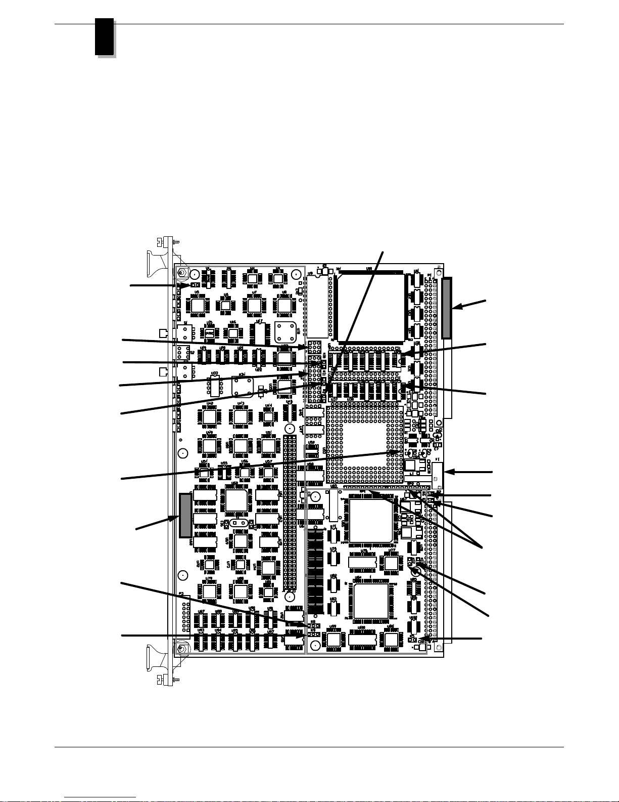
A layout for the PT-VME161 is shown in “Figure 1: PT-VME161 Device Positions”. The model
PT-VME161 and PT-VME161E are two versions of the same PCB with different component options.
There are various jumpers to configure user options which must be set before initial bootup. Refer to the
information in this section to verify that you have the correct settings.
Device Positions
K2
K1
K3
K10
K4
K11
Serial
No.
Assy
Rev
Label
U24
Caution:
Note Orientation
U36
Caution:
Note Orientation
F1
K6
K7
SCSI
TERM
K8
K9
Figure 1: PT-VME161 Device Positions
12 Extensible Single Board Computer/Controller User’s Manual
K13
K12
K5
Page 27
Performance Computer
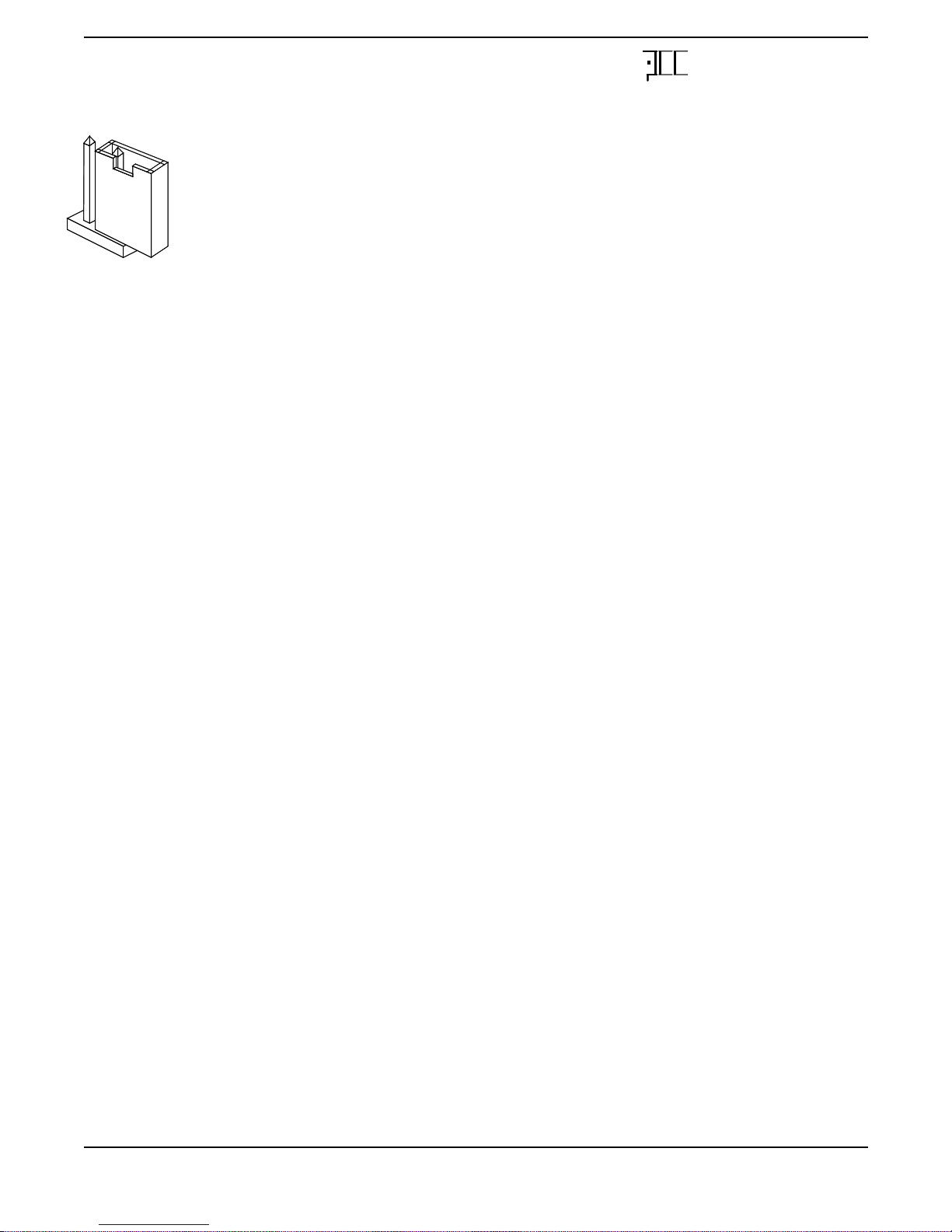
All Jumper Blocks are designed to mate with standard 2 pin jumper shunts. Spare jumper shu nts can be stored
by slipping one side o f the jumper s hunt on a sing le, unu sed pin of a j umper bloc k and allowi ng the other si de
of the jumper shunt to hang in space. As shown at left:
Extensible Single Board Computer/Controller User’s Manual 13
Page 28
Section
2
GETTING STARTED
U24 PROM/ROM/SRAM/EEPROM Socket Configuration
Locations U24 and U36 both pr ovide suppor t f or read only d evices such as ROM, PROM, EPROM, and
Flash EPROM. Location U24 has additional su pport for read/write devices as wel l, SRAM and non-volatile SRAM.
The positions of locations U2 4 and U36 are i den tif ied i n Fig ure 1 : on pag e 12 and Figure 2: on page 14.
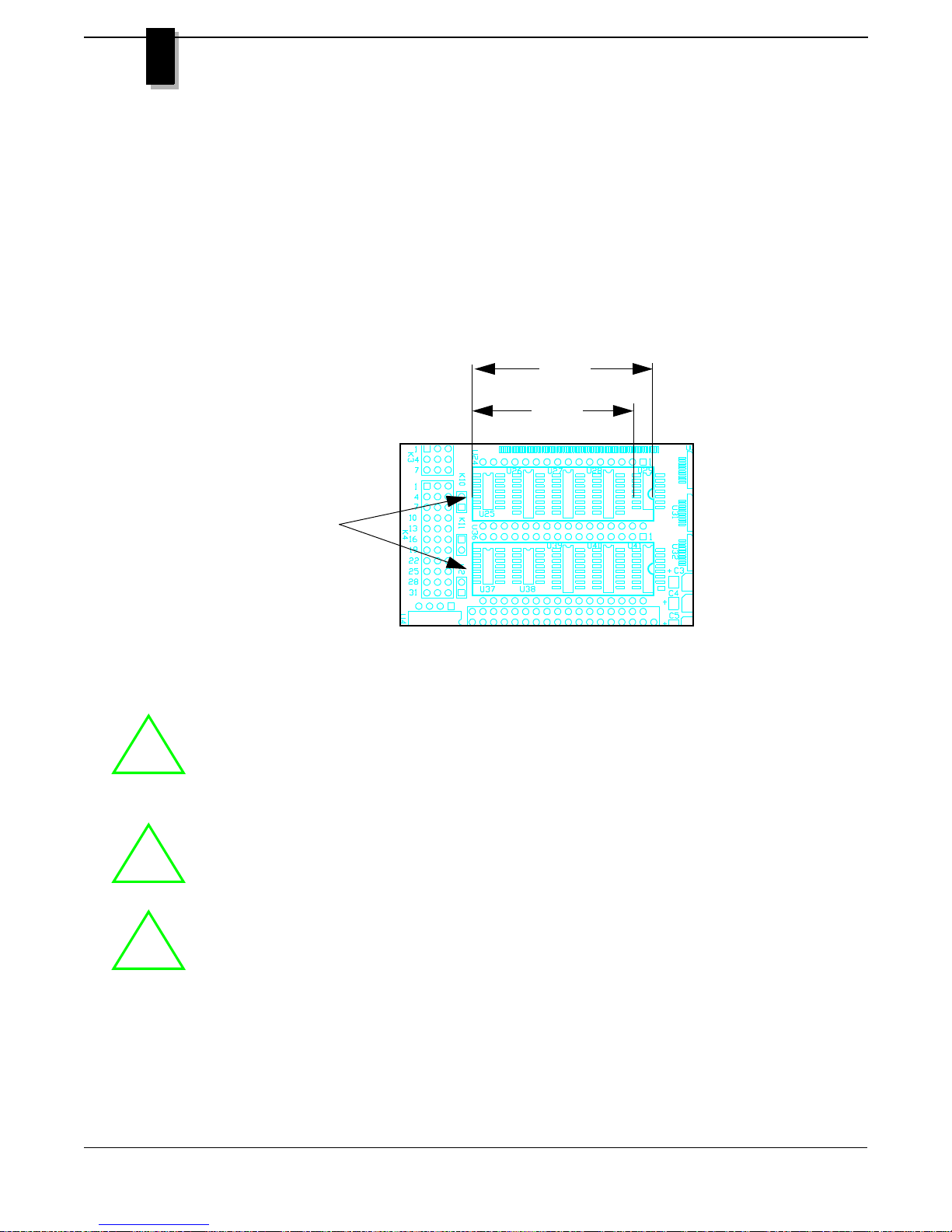
Both locations are capable of supporting 32 or 28 pin devices. The figure b elow demonstrates the neces-
sary pin alignment for the respective devices. See CAUTIONS below!
Figure 2: EPROM/ROM/SRAM/EEPROM Device Orientation
32-pin
28-pin
!
!
!
BOTTOM
CAUTION: WHEN INSERTING 28 OR 32 PIN DEVICES INTO LOCATIONS U24 OR U36 NOTE
THE ORIENTATION OF THE CHIP! THE BOTTOM OF THE CHIP WILL BE ALIGNED WITH
THE BOTTOM OF THE SOCKET STRIPS. THE “BOTTOM” OF THE SOCKET STRIPS ARE THE
ENDS FURTHEST FROM THE VME CONNECTORS. PIN 14 OF A 28 PIN DEVICE SHOULD
ENTER PIN 16 OF THE SOCKET.
CAUTION: PIN ONE OF THE CHIP SHOULD BE POINTING TOWARDS THE VME CONNECTORS.
CAUTION: THE DEVICE MUST HAVE AN ACCESS TIME OF LESS THAN OR EQUAL TO 200
NS.
14 Extensible Single Board Computer/Controller User’s Manual
Page 29
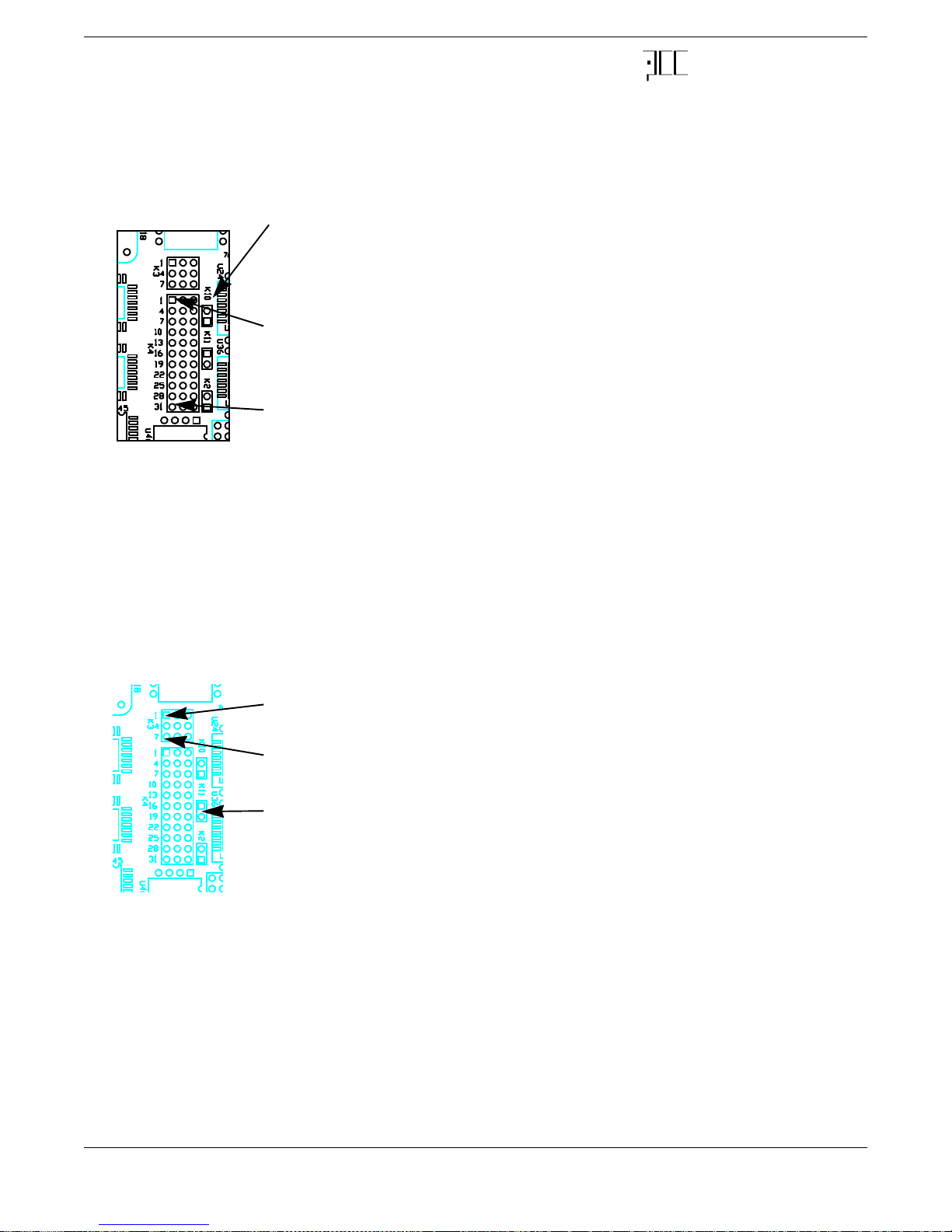
Location U24 Setup
Figure 3: K4 and K10Jumpers
K10
K4 - Jumper 1
(Pin 1)
K4 - Jumper 3
The orientation of figure 3 is with the VMEbus connectors on the right.
Performance Computer
The pin out configuration for location U24 is defined by Jumper Blocks
K4 and K10. There are eleven jumpers at location K4 and a single jumper
at K10.
Each K4 jumper position consists of a row of three adjacent pins. The
Jumpers are numbered from 1 to 31 starting with Jumper 1 at the pin 1
end of the Jumper Block K4. In fi gure 3, pi n 1 is in the upp er left corn er.
K4 pins are numbered from left to right and top to bottom.
There are three possible states for each jumper: the center pin shorted to
the left pin (bottom justified jumper sh unt in figure 5), the center pin
shorted to the right pin (top justified jumper shunt in figure 5), or all three
pins unconnected (no jumper shunt in figure 5).
Jumper Block K10 is a simple two pin jumper where the pins are either
open or shorted.
Figure 5 displays a schemati c representation of K4 and K10 jumpers for typical U24 co nfigurations .
Location U36 Setup
Figure 4: K3 and K11 Jumpers
K3 - Jumper 1
(Pin 1)
K3 - Jumper 3
K11
The orientation of figure 4 is with the VMEbus connectors on the right.
The pin out configuration for location U36 is defined by Jumper Blocks
K3 and K11. There are three jumpers at location K3 and a single jumper
at K11.
Each K3 jumper position consists of a row of three adjacent pins. The
Jumpers are numbered from 1 to 3 starting with Jumper 1 at the pin 1 end
of the Jumper Bloc k K3. I n f igure 4, pin 1 is in the upp er lef t corn er. The
pins are numbered from left to right and top to bottom. The orientation
of figure 4 is w ith the VMEbus connectors on t he right.
There are two possible states for each jumper: the center pin shorted to
the right pin (bottom justified jumper shunt in figure 5) or the center pin
shorted to the left pin (top justified jumper shunt in figure 5).
Jumper Block K11 is a simple two pin jumper where the pins are either
open or shorted.
Figure 5 displays a schemati c representation of K3 and K11 jumpers for typical U36 co nfigurations .
Extensible Single Board Computer/Controller User’s Manual 15
Page 30
Section
2
GETTING STARTED
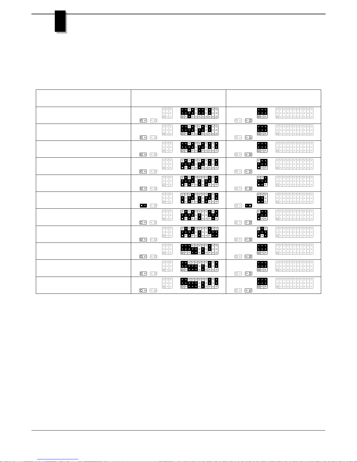
Figure 5 displays Jumper Blocks K10, K4, K11, and K3 from the component side of the PCB. The
pattern represented below is viewed when the PT-VME161 is placed on a work surface component
side up and the Front Panel closest to the observer. “*” indicates factory configuration.
Figure 5: U24 and U36 Jumper Settings
Device Type
32Kx8, 28 pin
PROM/ROM
* 64Kx8, 28 pin
PROM/ROM
128Kx8, 32 pin
PROM/ROM
256Kx8, 32 pin
PROM/ROM
512Kx8, 32 pin
PROM/ROM
512Kx8, 32 pin, Flash EPROM
Vpp = 5V
All other 32 pin Flash EPROMs
Vpp = 5V
32 pin1 Flash EPROMs
Vpp = 12V
8Kx8, 28 pi n
SRAM/EEPROM/RTC
32Kx8, 28 pin
SRAM/EEPROM
128Kx8, 32 pin
SRAM/EEROM
U24 Jumper Positions
K10 K11 K3 K4
10131619222528
1 4 7
1 4 7
1 4 7
1 4 7
1 4 7
1 4 7
1 4 7
1 4 7
1 4 7
1 4 7
1 4 7
1 4 7
10131619222528
1 4 7
10131619222528
1 4 7
10131619222528
1 4 7
10131619222528
1 4 7
10131619222528
1 4 7
10131619222528
1 4 7
10131619222528
1 4 7
10131619222528
1 4 7
1 4 71013161922252831
1 4 71013161922252831
U36 Jumper Positions
K10 K11 K3 K4
31
31
31
31
31
31
31
31
31
1 4 7
1 4 7
1 4 7
1 4 7
1 4 7
1 4 7
1 4 7
1 4 7
1 4 7
1 4 7
1 4 7
10131619222528
1 4 7
10131619222528
1 4 7
10131619222528
1 4 7
10131619222528
1 4 7
10131619222528
1 4 7
10131619222528
1 4 7
10131619222528
1 4 7
10131619222528
1 4 7
10131619222528
1 4 7
1 4 71013161922252831
1 4 71013161922252831
31
31
31
31
31
31
31
31
31
16 Extensible Single Board Computer/Controller User’s Manual
Page 31
SCSI Termination
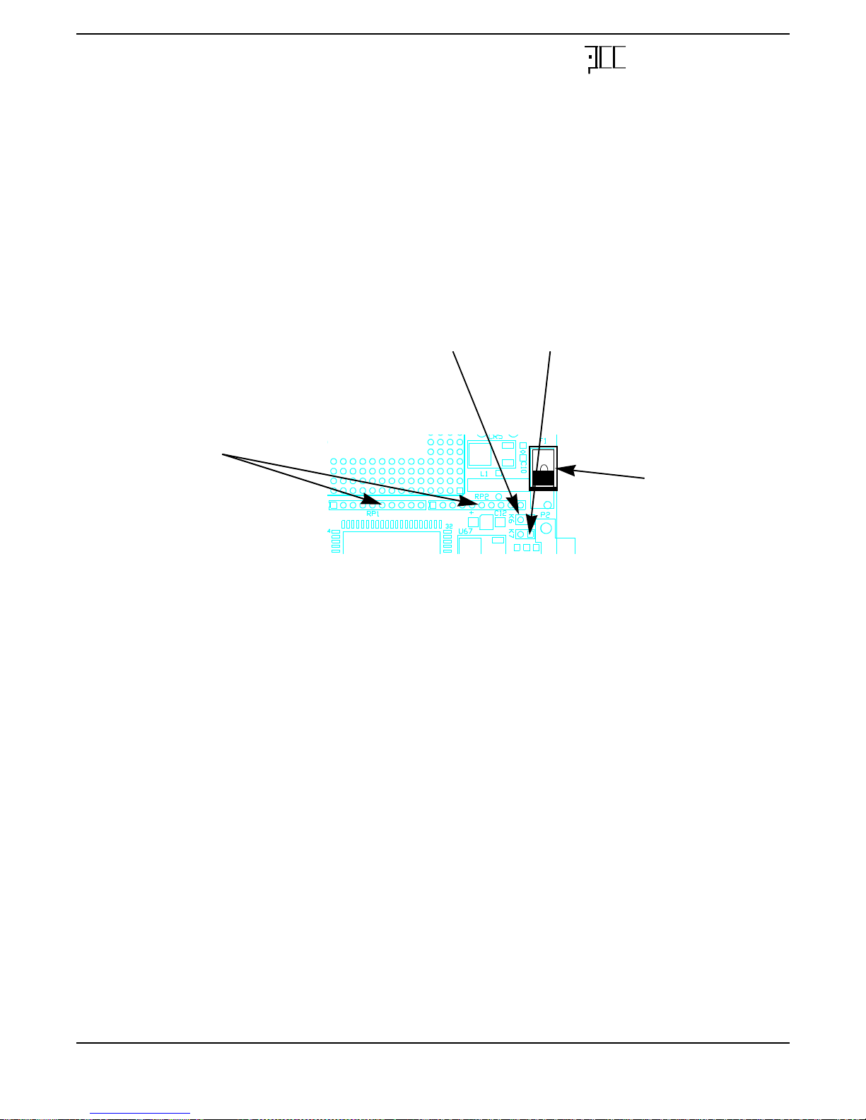
The configuration shipped from PTI assumes that the PT-VME161 is at the end of the SCSI cable,
providing termi nat ion and the terminator po wer i s provided directly from t he bo ard’ s +5V supply, SCSI
Termination resistor packages RP1 and RP2 are installed and Jumper K6 is set appropriately.
If the PT-VME161 does not need to terminate the SCSI cable then see “Disabling Termination” below.
You might want to review the section “Termination Power Source” if you are going to be bringing the
PT-VME161 up and down and there are other SCSI Initiators attached to the SCSIbus.
SCSI
Termination
Resistor Packs
Performance Computer
Figure 6: SCSI Components
Jumper K6 Jumper K7
SCSI
Terminator
Fuse
Disabling Termination
If the PT-VME161 is not at one end of the SCSI cable then the termination will be supplied by
another SCSI device and, SCSI Termin ation resi stor packages RP 1 and RP2 (shown above) must be
removed.
Termination Power Source
The active termination circuit on the PT-VME161 draws its power from the SCSI TERMPWR
signal pin. For proper termination some device on the SCSI cable must supply +5V on the
TERMPWR line. Through jumper K6 the PT-VME161 is capable of doing this. With pins 1 and 2
of K6 shunted the power is provided to TERMPWR pin directly by the board’s +5V supply. When
the pins 1 and 2 are open another device on the SCSI bus must supply TERMPWR. See
“TERMPWR Overview” below for more information.
TERMPWR Overview
There are two classes of devices on a SCS bus, Initiators and Targets. The SCSI controller on
the PT-VME161 can act as either but it typically is an initiator. Disk drives, tape drives, etc. are
Extensible Single Board Computer/Controller User’s Manual 17
Page 32

Section
2
GETTING STARTED
normally target devices. W ith a single t arget (disk drive) and a single initiator (the PT-VME161)
on a SCSIbus, termination is provided by the respective devices at each end of the cable. If
either end were to lose power then termination would be moot because there would be no data
to transfer.
Multiple PT-VME161s have been tied together on a single SCSIbus to use the SCSIbus as a
very high performance Local Area Network. In this application it was advantageous to be able
to power down an individual PT-VME161 withou t having to worry about whether it was the one
supplying the SCSIbus termination. The SCSI TERMPWR mechanism provided the sol ution.
The PT-VME161’s +5V supply goes thr ough fuse F1 then diode CR2 t o be OR’ed into the SCSI
TERMPWR signal. This allows the PT-VME161 to supply SCSIbus termination power when it
is powered up and some other device on the SCSIbus to provide it when it is not. The fuse
protects the PT-VME161’s power supply from short circuit conditions on the TERMPWR
signal.
If for some reason you do not want the PT-VME161 to contribute to TERMPWR remove fuse
F1. Fuse F1 is removed by pulling it to the right as shown by the bidirectional arrow on top of
it in Figure 6.
NOTE: If unreliable SCSI operation occurs, the fuse, terminator resistor packs and jumper
settings should be checked.
18 Extensible Single Board Computer/Controller User’s Manual
Page 33
Performance Computer
DRAM Module Upgrading
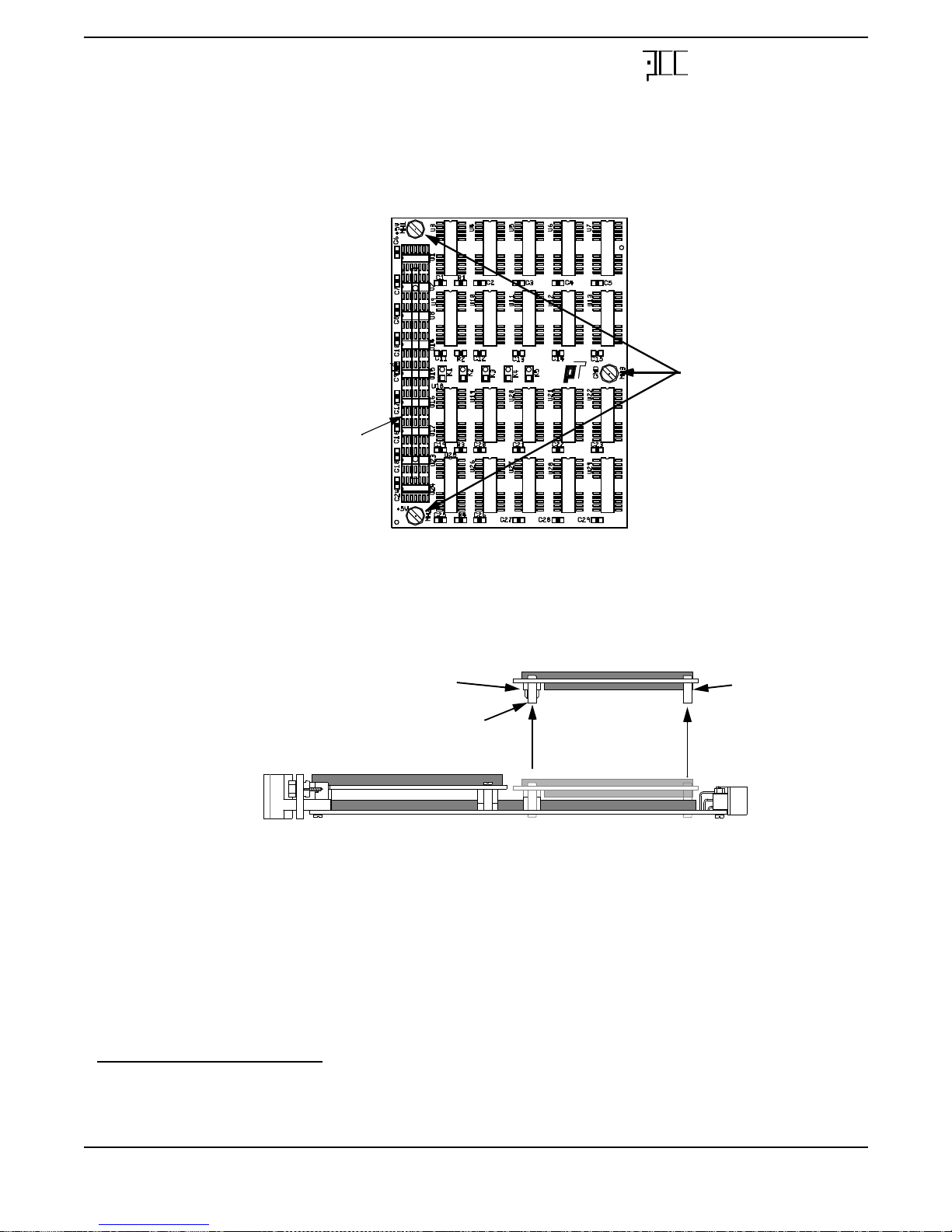
The DRAM module is designed to be easily upgraded by the user1. The low insertion force 80 pin surface
mount connection to the PT-VME161 allows the module to be snapped on.
Standoffs
Base Module Connector
(underside of board)
2
There are three standoffs
that support the DRAM module. To upgrade the DRAM module, place the
PT-VME161 on a work surface component side down and remove the three screws from the standoffs.
Turn the board over and pop off the DRAM module by lifting it straig ht up from the boa rd. In the drawing
below the grayed area indicates the “component” side.
Base Module
Connector
Standoff
DRAM Module
Standoffs
Optional EPAK
PT-VME161 Base Module
To install the new DRAM module, place the PT-VME161 on a work surface component side up. Carefully align the bodies of the DRAM module connectors, and press firmly on top of the connector with
both thumbs to snap it in. Check to see that the DRAM Module connector is tightly seated. The standoff s
should be flush with the surface of the PT-VME161.
Turn the PT-VME161 with the attached DRAM Module over (component side down) then install and
tighten the three screws into the standoffs.
1
The jumpers (K1-K5) on the DRAM Module are factory configured, no user modifications are required.
2
Standoff - A threaded tube with a screw in each end.
Extensible Single Board Computer/Controller User’s Manual 19
Page 34

Section
2
GETTING STARTED
NOTE: All 3 standoffs must be properly installed because they are also used to carry power and ground
to the DRAM Module.
EPAK Installation
If not already installed do it now! Follow the instructions contained in your EPAK User’s Manual.
20 Extensible Single Board Computer/Controller User’s Manual
Page 35
Board Installation
Power Considerations
The PT-VME161 typically draws 25 ma. of +12V and -12V, and 3.9 Amps of +5V. These figures must
be added to those of any attached EPAK or EBOARD to determine the total power requirements. It is
recommended that Maximum values are used to ensure adequate margins. Add these numbers to those
of the other devices in the system and check that the incorporation of the PT-VME161 (and Option
Modules) does not exceed the system power supply ratings.
NOTE: On the PT-VME161 both 12V supplies are used by the RS-232 drivers attached to the DUART
and passed to the EPAK connector. +12V can also be used by EPROMS that require a VPP = 12V.
Slot Considerations
If you plan on using t he System Cont roller funct ions of the PT-VME1 61 then it mu st be plugge d into the
Slot 1 position of t he VME backplane. The S ystem Controller function s will be aut omatically enabled
after reset if the Slot 1 [BG3IN*] signal is open (or grounded).
Performance Computer
For applications that do not require system controller functions the PT-VME161 can reside in any other
VMEbus Slot. There are two considerations that must be made when not using the PT-VME161 in Slot
1, any jumpers on the backplane for the Bus Grant and Interrupt Priority chains must be removed, and
the choice of slot location can effect the system level performance of the board.
Relative to other devices at the same Bus Grant and Interrupt Priority levels, the priority of a board goes
down as it moves away from Slot 1. Typically, slot position only becomes an issue when there are
extremely high levels of bus activity. The slot position, bus grant and interrupt priority levels should be
reviewed from a system perspective whenever a new board is configured into a system.
Backplane Insertion
WARNING: The chassis must be switched off before inserting the board or making any cable connections to avoid damage to yo urself or the components!
After reviewing the Power Considerations and selecting a slot, insert the PT-VME1 61 into the backplane.
Be sure that it is seated completely into the backplane then tighten the two Captive Chassis Mounting
Screws on the front panel. See “Figure 9: Example Serial port Cable” on page 26. Attach cables as necessary then power up the system.
NOTE: The first time the system is powered up after inserting the card, check the supply voltages at the
PT-VME161 backplane P1 and P2 connectors. Adjust the supplies as necessary to the nominal voltage
levels (+12.00V, - 12.00V and +5.00V)
Extensible Single Board Computer/Controller User’s Manual 21
Page 36
Section
2
GETTING STARTED
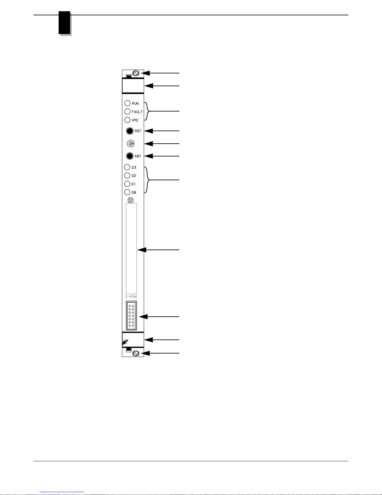
Figure 7: PT-VME161 Front Panel
Captive Chassis Mount Screw
PT-VME
161
Ejector Handle
System Status Indicators
RESET Switch
Rotary Switch
ABORT Switch
User Programmable LEDs
VME64
Performance
Technologies
Optional EPAK I/O Connector
RS-232 Utility Port
Ejector Handle
Captive Chassis Mount Screw
22 Extensible Single Board Computer/Controller User’s Manual
Page 37

SCSI Considerations
Cabling
The PT-VME161 SCSI interconnect is provided through the User Defined Signal pins of the VMEbus
P2 connector. The signals are organized so that a mass terminated Insulation Displacement Connectors
(IDC) can be used to attach SCSI devices to the PT-VME161. See “Table 13: VMEbus” P2” Connections” on page 77.
An interface cable can be constructed using a 50 conductor ribbon cable to attach a Eurocard (DIN 4612)
IDC with only rows A and C populated to a 50 contact ribbon cable IDC socket. The VMEbus User
Definable signals occupy 64 of the 96 positions on the P2 connector (rows A and C), however the SCSI
specification only requir es 50 condu cto rs , so pi n- 1 of t he ribbon cable must be justified to the pin- 1 end
of the Eurocard connector.
The SCSI Specification specifies that the maximum end to end length of a single-ended (TTL) SCSIbus
cannot exceed 6 meters or 19.69 ft.
Example
Performance Computer
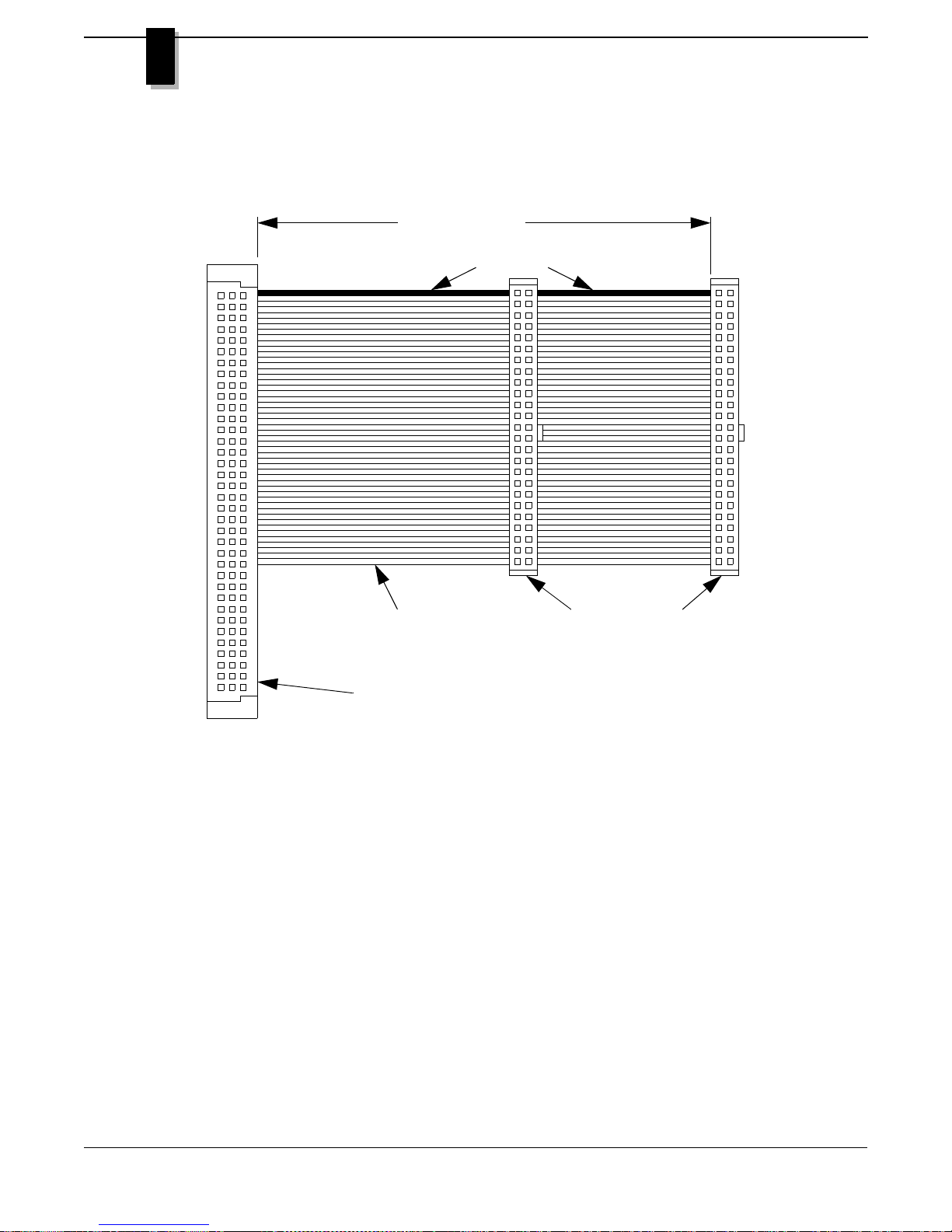
Following is an example cable with vendors and part numbers for the components. These configurations have been tested at PTI. Figure 9 displays an example SCSI cable for the PT-VME161. The
view is with the connector sockets poin ting towards you.
As long as the 6 meter maximum length identified in the SCSI specification is not exceeded there
are no constraints on the spacing between connectors other than those imposed by your physical
configuration. It is recommended that the cable be no longer than necessary for your particular application. The SCSIbus i s bas ically asy nchrono us, so long cable le ngths do contri but e to cont rol si gnal
handshaking delays, affecting the overall performance.
VMEbus P2 Connection
64 position Insulation Displacement Connector derived from DIN 41612 type C, with rows A
and C populated (socket):
Burndy BPS3B96ACROFS Z1 or
AMP 746603-1
Ribbon cable
50 Conductor 28 AWG. Flat Cable
Spectra-Strip 843-191-2801-050 or
3M 3365/50
SCSI device connector
50 Pin Flat Cable Connector center polarized
Burndy FRS50BF-8 (strain relief included) or
Extensible Single Board Computer/Controller User’s Manual 23
Page 38
Section
2
GETTING STARTED
AMP 1-746288-0 (connector)
AMP 499252-4 (strain relief)
Figure 8: Example SCSI Cable
6 Meter Maximum
A B C
Pin 1 Indicator
1
50 Conductor Ribbon Cable
64 Pin VMEbus “P2” Connector
1 1
50 Pin Flat Cable Connectors
for SCSI devices (up to 7)
Mechanical restraints
Depending upon your mechanical configuration, tie wraps or cable clamps may be necessary to
provide mechanical support for the cable. Most VME backplanes and SCSI devices do not provide
locking mechanisms or other means of mechanically securing the connectors. They depend on the
insertion force of 50+ pin and socket connections to hold the attached connector and cable in place.
Nothing is more frustrating than intermittent errors d ue to a connector that ha s been pulled out by
the weight of its own cable.
PTI recommends that, if possible, you attach the cable to some nearby metal work with tie wraps or
cable clamps to provide mechanical support for the cable, especially if it is long (more than 1 8 inches
between device connections) or if it is in a high vibration environment.
SCSI device grounds
Most SCSI device vendors provide a method for connecting their device to chassis ground. It is
suggested that you follow the vendor’s recommendations for its use. Proper use of these connections
generally improves the overall noise margins of a system.
24 Extensible Single Board Computer/Controller User’s Manual
Page 39
Device addresses
Check the device addresses of all SCSI devices to ensure that no conflicts occur. The device address of
the PT-VME161 is programmable and will be determined by yo ur installed software.
Serial Port Cabling
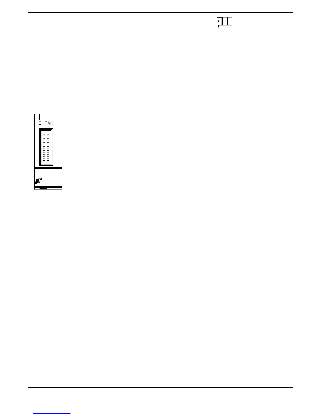
The PT-VME161 Utility Serial Port interconnect is provided on the front panel. The signals are organized so that a mass terminated Insulation Displacement Connectors (IDC) can be used to create an RS232 DTE interconnect. See “Table 11: Utility Serial Port Pin Assignments” on page 75. A 12 inch transition cable is supplied wi th the PT-VME161 which converts between the 14-pin header and a female
shell (male pin) 25-pin D-Shell connector. If a longer cable or a different D-Shell connector sex is
1314
12
10
8
6
4
11
9
7
5
3
12
required it can be assembled by f ollowing t he example b elo w. The Utility P ort pin posi tions are note d in
the figure to the left.
The EIA/RS-232C Specification limits the maximum end to end cable length to 50 ft.
Performance Computer
VME64
Performance
Technologies
Example
Following is an example cable with vendors and part nu mbers for the co mponents. These config urations
have been tested at PTI. Figure 9 displays an example serial cable fo r the PT-VME16 1. The view is with
the connector sockets pointing towards you.
An interface cable can be constructed using a 14 conductor ribbon cable to attach a 25-Pin D-Shell IDC
to a 14 contact ribbon cable IDC socket. To conserve front panel space only a 14 pin connector is used,
however the 25-Pin D-Shell expects 25 conductors, so pin-1 of the ribbon cable must be justified to the
pin-1 end of the D-Shell connector. It is reco mmended that the cable be no longer than necessary for yo ur
particular application.
D-Shell Connection
25 position Insulation Displacement Connector Male, D-Shell connector derived from DIN 41612
type C, with rows A and C populated (socket):
3M 8225-6003 or
T&B 609-25P-MA2
Ribbon cable
14 Conductor 28 AWG. Flat Cable
Spectra-Strip 843-191-2801-014 or
3M 3365/14
RS232 Serial Port connector
14 Pin Flat Cable Connector center polarized
Extensible Single Board Computer/Controller User’s Manual 25
Page 40
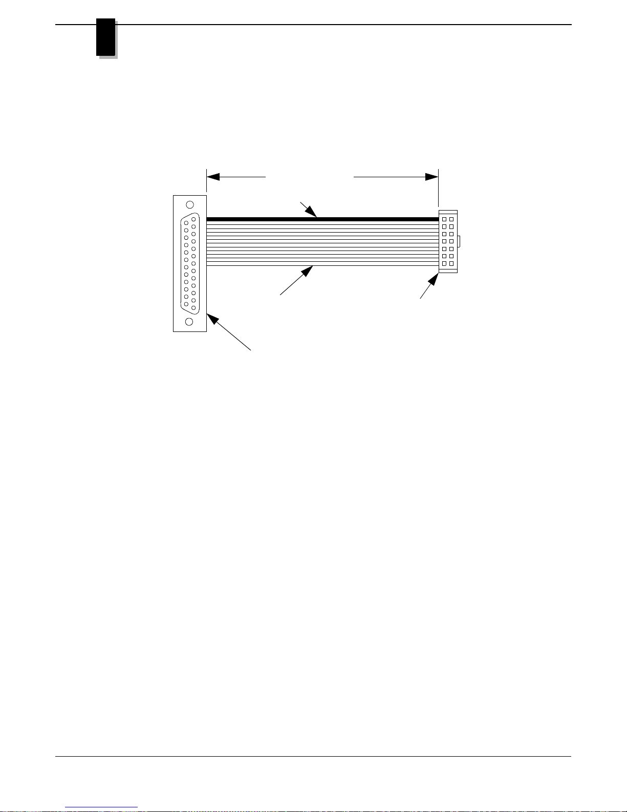
Section
2
GETTING STARTED
Burndy FRS14BF-8 (strain relief included) or
AMP 746288-2 (connector)
AMP 499252-9 (strain relief)
Figure 9: Example Serial port Cable
50 Foot Maximum
Pin 1 Indicator
1
14 Conductor Ribbon Cable
25 Pin D-Shell Connector
14 Pin Flat Cable Connector
1
Mechanical restraints
Depending upon your mechanical configuration, tie wraps or cable clamps may be necessary to provide
mechanical support for the cable.
26 Extensible Single Board Computer/Controller User’s Manual
Page 41
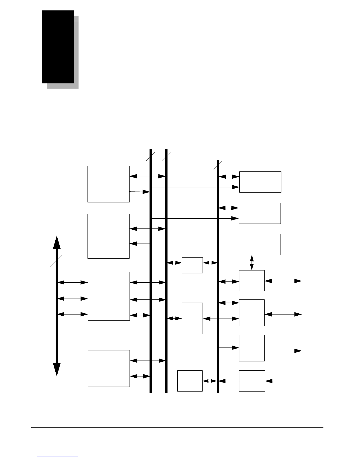
Section
3
FUNCTIONAL DESCRIPTION
A block diagram of the PT-VME161 is provided below. Down the center are the 32-bit microprocessor
address and data busses. To the right is an 8-bit buffered data bus that provides I/O interface connectivity.
To the left is the VMEbus interface, provided by the Advanced VMEbus Interface Chip Set.
Figure 10: Block Diagram
32-bit Microprocessor Data Bus32-bit Microprocessor Address Bus
8-bit Buffered Data Bus
MC68060
or
MC68EC060
Timekeeping
RAM
PROM/SRAM
Sockets
VMEbus
Control
Address
Data
4,8,16,32 or 64
MB Dual Ported
DRAM
SCV64
EPAK
Interface
8-bit
Buffer
16-bit
Buffer
82C54
Interval
Timer
Serial
EEPROM
DUART
68681
FAS216
System
Control
Register
System
Status
Register
2 RS-232
SIO Ports
(Front Panel)
Single-Ended
SCSI 2
(P2)
User LEDs &
Control bits
Hex Switch
Extensible Single Board Computer/Controller User’s Manual 27
Page 42

3
Section
FUNCTIONAL DESCRIPTION
Through the remainder of this document references to the Motorola MC68060 processor imply the
MC68EC060 also. Specific differences will be cited as necessary.
Microprocessor
The PT-VME161 utilizes a Motorola MC68060 microproces sor running at 50 MHz. This processor
combines a full 32-bit Central Processing Unit (C PU) core, a data cache, a n instruction cache, a Floating
Point Processor, and an enhanced bus controller in a single VLSI device. The MC68EC060 is identical
to the MC68060 except that it lacks the MMU and FPU. The MMU of the 68060 may be disabled by
installing jumper K2.
Memory
There are four separate memory mechanisms available on the PT-VME161: up to 64 megabytes of
DRAM, two 32-pin JEDEC sockets for ROM, PROM, EPROM, etc., 8184 bytes of nonvolatile SRAM,
and 128 bytes of nonvolatile EEPROM.
DRAM
The main memory is composed of 70 ns. fast page mode DRAM. Available memory configurations are
4, 8, 16, 32, or 64 megabytes of DRAM. All of main memor y can be mapped t o the VMEbus throug h the
SCV64. Additionally, EPAK address space may be mapped t o the VMEbus by overlaying its address
space with a portion of main memory. The overlaying is enabled at reset, making a portion of the main
memory inaccessible for the VMEbus. If the ability to address the EPAK from the VMEbus is not
desired, it may be removed by writing a 1 to the Enable EPAK Access from VME bit (0) of Control
Register 2. See “Enable EPAK Access from the VMEbus” on page 46 for more information.
The 68060 and 68EC060 support a burst mode for filling th eir on-chip data and instruction caches. The
PT-VME161 utilizes the fast page mode of the DRAM to accelerate the bu rst transfer o peration. Dur ing
a burst transfer four sequential long words are fetched from the DRAM, requiring four clock cycles for
the first long word transfer and two clock cycles for subsequent long word fetches.
1
is generated and checked by PT-VME1 61 hard ware on local DRAM Accesses by the MC68060.
Parity
A Bus Error may be generated as an acknowledgement to a reference if a parity error is detected. See
“Parity” on page 30 for more information.
The address space from 20000000h to 2FFFFFFFh is allocated to the DRAM. Any reference to this 256
MByte space will complete without a bus error. The installed DRAM will repeat throughout this range.
Repeatability is described below. ‘Blank’ areas of memory canno t be written an d will ret urn unpredictable results when read. The DRAM size may be determined by reading the Status Register.
1
Not availiable on 4M and 8M Configurations.
28 Extensible Single Board Computer/Controller User’s Manual
Page 43

DRAM Mapping
DRAM Size Address Range Response
4 MBytes 20000000-203FFFFFh Normal
20400000-20FF FFFFh Blank
21000000-213FFFFFh Normal - repeat of 20000000-203FFFFF
21400000-21FFFFFFh Blank
The pattern of (4M Normal) - (12M Blank) - (4M Normal) - (12M Blank) repeats
throughout the range of 20000000- 2FFFFFFFh. Th us address 2 0000000h may be read
or written at 21000000h, 22000000h, etc.
8 MBytes 20000000-207FFFFFh Normal
20800000-20FF FFFFh Blank
21000000-217FFFFFh Normal - repeat of 20000000-207FFFFF
21800000-21FFFFFFh Blank
The pattern of (8M Normal) - (8M Blank) - (8M Normal) - (8M Blank) repeats
throughout the range of 20000000- 2FFFFFFFh. Th us address 2 0000000h may be read
or written at 21000000h, 22000000h, etc.
Performance Computer
16 MBytes 20000000-20FFFFFFh Normal
21000000-21FFFFFFh Normal - repeat of 20000000-20FFFFFF
The pattern of (16M Normal) - (16M Normal) repeats throughout the range of
20000000-2FFFFFFFh. Thus address 20000000h may be read or written at
21000000h, 22000000h, etc.
32 MBytes 20000000-21FFFFFFh Normal
22000000-23FF FFFFh Blank
24000000-25FFFFFFh Normal - repeat of 20000000-21FFFFFF
26000000-27FF FFFFh Blank
The pattern of (32M Normal) - (32M Blank) - (32M Normal) - (32M Blank) repeats
throughout the range of 20000000- 2FFFFFFFh. Th us address 2 0000000h may be read
or written at 24000000h, 28000000h, etc.
64 MBytes 20000000-23FFFFFFh Normal
24000000-27FFFFFFh Normal - repeat of 20000000-23FFFFFF
The pattern of (64M Normal) - (64M Normal) repeats throughout the range of
20000000-2FFFFFFFh. Thus address 20000000h may be read or written at
24000000h, 28000000h, etc.
Sizing
To size DRAM perform the following steps:
Step 1 Write location 20000000h with AA55AA55h.
Step 2 Set Memory pointer to 20400000h
Extensible Single Board Computer/Controller User’s Manual 29
Page 44

Section
3
FUNCTIONAL DESCRIPTION
Step 3 Write CC33CC33h to the longword pointed to by the Memory Pointer.
Step 4 Read the location pointed to by the Memory Pointer.
Step 5 Add 00400000h to the Memory pointer to step it to the next 4 MByte boundary.
Step 6 Done.
If the value read back value does not equal CC33CC33h then the end of memory
has been reached. Go to Step 5.
If the read back value does match CC33CC33h then check location 0 to see if it
still contains AA55AA55h. If location 0 equals CC33CC33h then t he end of memory has been reached. Go to Step 5.
If location 0 equals AA55AA55h then the end of memory has not been reached.
Go to Step 4.
Go to Step 2.
Parity
Parity RAM is provided for the 16, 32, and 64 MByte configurat ions. Parit y is generated and checked on
all DRAM accesses, which include accesses by the 68060, SCV64, SCSI controller, and EPAK bus
masters.
Parity errors detected during 68060 reads or reads by an EPAK bus master return a bus err or. Parity errors
detected during a SCV64 or SCSI controller reference will assert the L7IMEM pin of the SCV64, generating a level 7 interrupt request. The source of the a parity error is latched in PT-VME161 System Status
Register 2. Parity errors that generate a Bus Error (68060 and EPAK bus masters) will not generate a
Level 7 interrupt however , the s ource of t he erro r will be latched i n St atus R egister 2. Any Level 7 in terrupts that do result from parity errors (SCV64 and SCSI controller) will remain as serted until Status
Register 2 is read. If a parity error is detected during a SCV64 local burst cycle, any rem aining Accesses
in the burst will be aborted by releasing the VMEGR signal to the SCV64.
NOTE: Status Register 2 must be read to determine the source of any Level 7 interrupt request, because
the SCV64 L7IMEM pin is also used to signal a SCSIbus Reset conditions.
Checking
Parity checking is enabled by setting the Enable Parity Error Checking (EPEC) bit in Control
Register 2 (bit 1). Parity checking is disabled following reset or if Parity RAMs are not installed (4M
and 8M configurations).
Parity is always written to DRAM regardless of the state of EPEC. If EPEC is disabled then level 7
interrupts and bus errors will not be g ene rated and t he asso ciated fl ags (bits 0-3 ) in Status R egi ster
2 will not be asserted.
30 Extensible Single Board Computer/Controller User’s Manual
Page 45

Performance Computer
Initialization
DRAM must be initialized before enabling parity error checking. The initialization process consists
of writing any data value to all installed memory locations. This operation sets the parity RAM to a
valid state.
Testing
For testing purposes bad parity may be intentionally written. By setting the Enable Bad Parity bit (2)
in Control Register 2, the parity bit written with each data byte will be complemented causing a
parity error to be generated when the byte is read.
NOTE: If EBP is enabled then the Enable Parity Error Checking (EPEC) must be disabled, otherwise parity errors will be generated on every memory reference.
Diagnostics should include checking parity on an individual byte basis to fully check the parity
RAM.
PROM/SRAM Socke ts
The board is equipped with two 32-pin JEDEC sockets configured as bytewide ports. Both sockets
support ROM, PROM, EPROM and Flash EPROM read-only devices, as well as 28-pin or 32-pin conf igurations.
One of the two sockets is also capable of supporting SRAM and Nonvolatile SRAM read/write devices.
Jumpers are provided to select between read-only and read/write operation and the 28-pin or 32-pin
configurations. See “ U24 PROM/ROM/SRAM/EEPROM Socket Configuration” on page 14.
Nonvolatile SRAM and Time of Day/Calendar Clock
The Dallas Semiconductor DS1643 Nonvolatile Timekeeping RAM features 8184 Bytes of Nonvolatile
SRAM and a Real Time Clock (RTC) with integrated crystal, power fail control circuit and a lithium
energy source. The clock registers are Accessed identical to the static RAM. The registers reside in the
top eight RAM locations. The the base address of the Timekeeping RAM is at 0F000000h. See “Table
7: DS1643 Nonvolatile Timekeeping RAM Registers” on page 71 for more information.
Serial EEPROM
The EEPROM supports 128 bytes of nonvolatile memory. The part is capable of 10,000 erase/write
cycles and ten year data retention. Performance Technologies normally uses this memory to store various
parameters and options used in the initialization and operation of the PT-VME161.
This device is socketed so that it can be moved to another board if necessary. For instance, if board level
replacement is typically performed on failures in the field, the EEPROM can be moved to the replacement board to maintain the configuration information of the original board.
Extensible Single Board Computer/Controller User’s Manual 31
Page 46
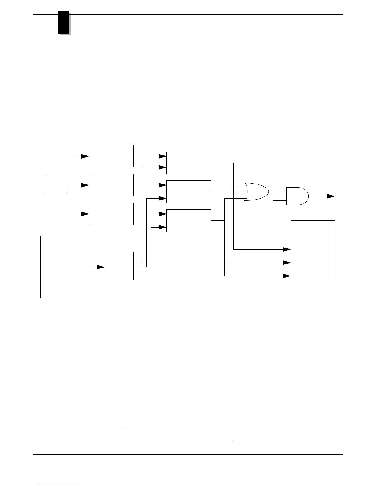
3
Section
FUNCTIONAL DESCRIPTION
Interval Timer
The Interval Timer, an Intel 82C54, provides three independent 16-bit timers running off the same 4 MHz
clock. These three timers are identical in operation. Refer to the Intel Peripherals Handbook
complete description of the 82C54
When an Interval Timer is programmed in “Mode 2”, it will perform the following functions when it
counts down to zero: pulse its OUTPUT pin, reload the initial count, and continue counting. The output
pulse of each timer is latched into the respective Interval Timer Interrupt Request Latch and the outputs
of the three latches are OR’ed together to generate the Interval Timer Interrupt Request.
2
.
for a
Figure 11: Interval Timer Block Diagram
4 MHz
Clock
System Control
Register 2
RITI0-RITI1
EITI
Interval Timer
0
Interval Timer
1
Interval Timer
2
decoder
The Interval Timer Interrupt Request generat es an interru pt t hrough t he LIRQ 2 pin of the SC V64. This
pin is shared with the SCV64 Tick Timer (which can b e disabled) . The Interval Timer Interrupt Request
can be enabled by setting the EITI bit (5) in System Control Register 2. When the Interval Timer interrupts are disabled, the latch ing of the ind ividual ti mer output pu lses is also di sabled. After reset, the stat e
of the 82C54 is undefined so the Interval Timer interrupts are disabled.
Output
Reset
Interval Timer 0
Request Latch
Interval Timer 1
Request Latch
Interval Timer 2
Request Latch
Interval Timer
Interrupt Request
System Status
Register 3
ITIP0
ITIP1
ITIP2
An interrupt on the LIRQ2 pin can be programmed (in the SCV64 Local Interrupts 3 and 2 Control
Register) to generate an auto-vector operation on any one of the 68060’s seven interrupt request levels.
Any of the Interval Timers may have its counting disabled by programming it to “Mode 1”. Mode 1
requires a rising edge on the timer’s GATE input to enable counting. Since each GATE input is hardwired to logic 1, Mode 1 will never count and thus may be used as a “Disable Counting” mode.
The current state of the individual Interval Timer Request Latches (0, 1, and 2) may be determined by
reading the Interval Timer Interrupt Pendi ng bits in System S tatus Register 3. SSR3 bits 4, 5, and 6 reflect
the state of ITIP0, ITIP1, and ITIP2, respectively.
2
See “Applicable Documents” on page 2 for Intel Peripherals Handbook ordering information.
32 Extensible Single Board Computer/Controller User’s Manual
Page 47

VMEbus Interface
The VMEbus interface provides VME64 data transf ers as well as a fully functional high performance 32bit VMEbus interface as defined by the IEEE 1014 Rev C VMEbus Specification. It is based upon the
SCV64 from Newbridge Microsystems.
See the SCV64 User Manual, the Newbridge Microsystems data book for more information.
SCV64
The SCV64 is a 64-bit interface to the VMEbus address and data buses with the local PT-VME161 bus.
It may act as a VMEbus Master or Slave. The local DRAM and EPAK address spaces of the PT-VME161
are accessible to a VMEbus Master through the SCV64. The SCV64 is also capable of DMA transfers
between local memory (DRAM or EPAK) and the VMEbus.
VME64 Transfers
VME64 is a newly defined capability of the VMEbus. VMEbus Block Transfer mode (BLT) only uses
the address bus during the first transfer cycle to pass the start address of the transfer. The slave is responsible for latching this address and incrementing it internally as subsequent data arrives. As a result the
address lines on the VMEbus are unused during all but the first transfer. Data is passed every transfer
cycle on the data bus.
Performance Computer
The 64 bit Multiplexed Block Transfer (D64MBLT) mode makes a minor change to the first cycle and
takes advantage of the address bus being otherwise unused during a block transfer data phase. A MBLT
cycle is divided into two phases, address and data. During the first transfer cycle address only is passed
and on all subsequent cycles data is passed. The combination of the 32 data lines, 31 address lines, and
the [LWORD*] signal provide a 64 bit path on the VMEbus. A double longwo rd can then be transfer red
on each Data Strobe/Data Acknowledge handshake. The address phase can be either A32 or A64. A32
transfers pass the address normally (on the address bus) and the 32 data lines are unused, A64 transfers
pass the high order 32 bits o f the 64 bit ad dress on the d ata lines. During th e data phase th e 31 address
lines, and the [LWORD*] signal are used to pass the high order 32 bits of the 64 bit data. Specific
Address Modifiers are used to identify A64:D64MBLT and A32:D64MBLT cycles.
Transfer Modes
The SCV64 is capable of two operational modes: “decoupled” and the traditional “atomic”. The
decoupled mode takes full advantage of the VMEbus bandwidth by using the receive and transmit
FIFOs, built into the chip, that decouple the local bus from the VMEbus. The FIFOs immediately
accept writes from one bus, release that bus for use, then finish the write to the destination bus. In
atomic mode the SCV64 bypasses the FIFOs, simply buffering the data and address to the destination bus, forcing any associated wait states back to the source bus.
All read, read-modify-write, and interrupt acknowledge cycles are atomic. To preserve data integrity, atomic cycles are not performed until all write cycles queued ahead of the atomic cycle are
completed.
Decoupled
This feature allows transfers on the VMEbus to be completely “decoupled” from any latencies
incurred on the local bus. VMEbus transfers can proceed at a rate that is determined strictly by
Extensible Single Board Computer/Controller User’s Manual 33
Page 48

Section
3
FUNCTIONAL DESCRIPTION
the VMEbus handshaking rate. The receive and transmit FIFOs can be individually enabled
using the RXATOM and TXATOM bits in the SCV64 Mode Control Register.
The receive FIFO captures write transfers from VMEbus devices or DMAC VMEbus reads.
Data can be moved into the FIFO using D64MBLT, D32BLT, D16BLT, or individual transfers.
As soon as there is data in the FIFO, the SCV64 requests the local bus and the data will be transferred to the appropriate address in DRAM or EPAK memory.
The transmit FIFO decouples local bus write references to the VMEbus, either from the CPU or
the DMAC. On DMA transfers you can optionally wait until the FIFO is full before writing to
the VMEbus. DMA data can be transferred from the FIFO using D64MBLT, D32BLT,
D16BLT, or individual transfer s. CPU references are always handled as individu al transfers. As
soon as there is data in the FIFO, the SCV64 requests the VMEbus and transfers the data to the
appropriate address.
If the FIFO Burst Enable (FIFOBEN) bit or DMA Burst Enabl e (D MABEN) bit in the SCV64
Mode Control Register is set then “burst mode” is used on the local bus to transfer the respective
data. Otherwise the incoming data will be moved as individual 32 bit references.
Atomic
When the RXATOM or TXATOM bit in the SCV64 Mode Control Regi ster is set, the respective FIFO is bypassed. In atomic mode, cycles are performed in direct-connected mode where
the address, data, DTACK and BERR signals are connected between the local bus and the
VMEbus.
VMEbus Control Logic
The VMEbus interface of the SCV64 is fully asynchronous, thus avoiding the delays and reliability
problems associated with synchronous designs. The VMEbus data transfer control lines Address
Strobe [AS*], Data Strobe [DS0* and DS1*] and Data Transfer Acknowledge [DTACK*] perform
asynchronous handshaking to pass data across the bus. Any delays in turning these handshaking
signals around slow down the associated data transfer. In the SCV64 fully asynch ronou s design, the
delays are strictly a function of propagation times through the control logic.
Synchronous design s require sampling of the VMEbus transfer cont rol signals in ord er to be reliably
used by the synchronous control logic. High sampling rates are necessary to achieve performance
equivalent to asynchronous designs, but these higher sampling rates increase the probability of metastability conditions occurring. When a metastable conditi on does occur its statis tical duration falls
off with time, therefore the longer that one waits to act upon the samp led signal the less likely they
are to see it metastable. A designer mu st make a perfo rmance vs. reliability trade of f on what this
delay should be. This Metastability Settling Time wil l add a fixed delay to every sampled signal.
Another delay added by s ampl ing is due to the sampli ng clo ck rate. An incoming sign al can change
anywhere between two sample clock edges. Best case is when the incoming signal changes just
before the sample clock, worst case is when the incoming signal just misses the sample clock. On
the average, a Sampling Delay of one half of the sample clock time must be added to each sampled
signal.
Therefore, every signal that requires sampling must have a Sample Delay and Metastability Settling
Time must be added to pro pagation times of the control l ogic. All synchron ous designs t hat inte rface
to the asynchronous VMEbus pay a performance penalty and make the associated performance vs.
reliability trade-offs.
34 Extensible Single Board Computer/Controller User’s Manual
Page 49

Performance Computer
VMEbus Slave Accesses
The Slave Image is the VMEbus address range throughout which the local memory of the board can
be accessed. The slave image of the PT-VME161 is defined in programmable registers of the
SCV64. Separate slave images, different in size, can be set up in the A64, A32 and A24 address
spaces. The SCV64 does not provide an A16 slave image. The respective slave images are defined
by base address and size registers. The A64 image base address can be programmed to start on any
4 gigabyte bound ary and is size 128 meg abytes in s ize. A64 address ing is on ly suppor ted during D64
Multiplexed Block Transfers (D64MBLT). The A32 image base address can be programmed to start
on any 128 megabyte boundary and be any size from 4 kilobytes to 128 megabytes in binary increments. The A24 image base address can start on any 512 kilobyte boundary or multiple of its
programmed size, whichever is larger, within the 16 megabyte A24 addressing space. The A24
image size can be programmed to 512K, 1, 2, or 4 megabytes.
The SCV64 responds to Standard and Extended, non-privileged and supervisory address modifiers.
VMEbus Access types include read, write and read-modify-write. Up to 128 megabytes of each
slave image can be protected from writes, or reads and writes.
Parity is generated and checked by PT-VME161 hardware on local DRAM Accesses by VMEbus
masters. A level 7 interrrupt may be generated if a parity error is detected. See “Parity” on page 30
for more information.
SCV64 register access from the VMEbus
The SCV64 provides a means for accessing its internal registers from the VMEbus. Since the DARF/
ACC did not support this feature, this capability is disabled on the VME161. Any attempts to access
SCV64 registers from the VMEbus will be treated as slave memory accesses and will access lo cal
VME161 DRAM. Note that this effectively disallows the use of the (new) SCV64 Mailbox registers.
The SCV64 AUTOBAR feature (powerup assignment of slave address) is not used.
EPAK access from the VMEbus
See “EPAK Interface” on page 57.
VMEbus Master Accesses
The SCV64 can request the VMEbus under a number of conditions: the transmit FIFO contains write
cycles, the DMAC starting transfers, the 68060 begins a read cycle to the VMEbus, the SCV64 is in
atomic mode and the 68060 begins a write cycle to the VMEbus, or the SCV64 was signaled with a
VMEbus [IACK*] to begin an interrupt acknowledge cycle.
The SCV64 provides an Ownership Timer which can be programmed to limit the time that the
SCV64 maintains VMEbus mastership, from immediately off to 2, 4, or 8 ms., to unlimited use. The
Ownership Timer is used to ensure predictable bus access latencies to other VMEbus masters.
While performing bus transactions from the FIFO the VMEbus “address pipelining” feature is used.
68060 Access es
CPU Accesses can be set up to be decoupled or atomic. In decoupled mode the FIFO accepts
the data, acknowledges 68060 writes then, the VMEbus immediately requests the bus. In atomic
Extensible Single Board Computer/Controller User’s Manual 35
Page 50

Section
3
FUNCTIONAL DESCRIPTION
mode the FIFO is bypass e d a nd t h e CP U wait s fo r the VMEbus acquisition and t rans fer to take
place. All 68060 reads bypass the FIFO.
Access to the VMEbus address space by the 68060 CPU is through addresses 80000000h FFFFFFFFh. In order to access the full VMEbus address space the Page bit in the 161 System
Control Register defines VMEbus address bit 31. When the Page bit is 0, PT-VME161
addresses 80000000h-FFFFFFFFh are mapped to VMEbus addresses 00000000h 7FFFFFFFh. When the Page bit is 1, PT-VME161 addresses 80000000h-FFFFFFFFh are
mapped to VMEbus addresses 80000000h-FFFFFFFFh.
For CPU Accesses the SCV64 splits 4 Gigabyte VMEbus address space into 32-128 megabyte
pages. Most pages are defined to be A32:D32, however selected ranges may define to be
A24:D32, A24:D16 and A16:D16 spaces.
CAUTION: When the CPU performs an Access in the A16:D16 range, the SCV64 will respond
!
to the CPU as a 16 bit device, unlike the 68030, the 68060 will NOT split up the cycles if necessary. Similarly, for references in the A24:D16 space.
A24:D32 and all A32 Accesses allow 32 bit transfers from the 68060. The implied addressing
space and the CPU function codes determine the data or program, and supervisory or nonprivileged aspects of the Address Modifier code.
Read-Modify-Write
The SCV64 is capable of s upp ort ing s in gle ad dres s Read-Modify-Write MC68060 i ns truct i on s
(TAS) across the VMEbus. The 68060 CAS and CAS2 instructions can require two addresses
during a “locked” operation, thus translating into a requirement for Address Strobe to be
asserted twice on the VMEbus while remaining “locked” in between. The VMEbus Specification provides no mechanism for supporting this class of operations.
DMAC
The DMA Controller in the SCV64 can transfer data between the VMEbus and DRAM or EPAK
memory in several different address and data modes. It is controlled through four internal registers:
DMA Local Address Register, DMA VMEbus Address Register, DMA Transfer Count Register,
and the SCV64 Mode Control Register.
The DMAC can be programmed to use A64, A32, or A24 addressing, in supervisor or nonprivilege
mode. The upper 32 bits of the A64 address are static and provided by the Master A64 Address
Register. The lower 32 bits of the A64 address and A32 or A24 ad dresses are provided by the DMA
VMEbus Address Register.
Data transfers can be programmed to occur in discreet (D32/D16), block (D32BLT/D16BLT), or
multiplexed block (D64MBLT) mode. Th e DMA Transfer Count Reg ister allows up to 4 megaby tes
of data to be transferred. The har dware automatically releases Address Strobe on the proper boundaries on the local and VMEbus.
To further improve transfer rates the PT-VME161 suppor ts “Burst Mode” transfers from the SCV64
on the local bus. Burst lengths of 4, 8, 16, or 32 longwords can be programmed using the BLEN field
of the SCV64 Mode Control Register. Given 32 longword bursts and the 4-2-2-2...2 DRAM burst
timing a maximum data transfer rate of 49.2 megabytes per second is achi evab l e over th e lo cal bus .
The DMA Burst Enable (DMABEN) and FIFO Burst Enable (FIFO BEN) bits in the SCV64 Mode
Control Register allow the “Burst Mode” feature of the individual mechanisms to be enabled.
36 Extensible Single Board Computer/Controller User’s Manual
Page 51

Performance Computer
The transfer rate over the VMEbus is a function of the master/slave handshaking rate and transfer
mode. When “decoupled” D64MBLT transfers were tested with the PT-VME240 VME64 Memory
Board a burst transfer rate exceeding 53 megabytes per second was measured.
DMA completions and errors can generate interrupts to the 68060, through interrupt handler of the
SCV64 ([- INTP<1>], LIRQ1).
The advanced features of the SCV64 can be used to tune DMAC and VMEbus performance. The
Transmit FIFO can be configured to begin VMEbus transfers immediately upon having data, or
configured to wait until the FIFO is full. The No-Release m ode (NOREL) bit in th e SCV64 Mod e
Control Register causes the SCV64 to maintain o wnership of th e VMEbus until either the SCV64
requests the SCV64 to release the bus, or until the bit is turned off. The Ownership Timer in the
SCV64 can be used in conjunctio n w ith the NOR EL bit to th rottle DMAC use of the VMEbus . By
using the DMA Burst Enable and FIFO Burst Enable bits the “Burst Mode” feature of the respective
mechanism can be enabled. The length of burst transfers on the local bus can be throttled with the
BLEN field of the SCV64 Mode Control Register. When bus snooping is enables (bit 7, system
CTRL Reg2), the burst lenght must be set to 4 (BLEN = 00) for proper snoop operation.
Parity is generated and checked by PT-VME161 hardware on local DRAM Accesses during DMAC
operation. A level 7 interrrupt may be generated if a parity er ror is detected. S ee “Parity” on page 30
for more information.
Location Monitor
The location monitor assists in inter-processor and inter-process communication. It consists of a 32bit wide, 31-entry deep message FIFO loaded from the VMEbus. D32 or D16 operations are
supported. If the even word is written, the upper 16 bits of the FIFO entr y are set to one. The message
FIFO is not bidirectional.
The Location Monitor exists at the top longword and the lower (even) word of the top longword in
each of the A32 and A24 slave images. The monitor is equally accessible by the VMEbus and the
local CPU. A process on the PT-VME161 does not need to determine whether the process it’s
sending a message to is local or not.
The existence of entries in the message FIFO can generate interrupts to the 68060, through interrupt
handler of the SCV64 ([- INTP<0>], LIRQ0).
Registers
The SCV64 is a longword wide device with 16 direc tly addressable intern al registers. Status bits are
generally sampled by the SCV64 at the start of a register access cycle to ensure up-to-date data for
the reference. Detailed descriptions of the r egisters ar e av ailable in th e SCV64 Tech nical Manu al, a
summary is provided in “Table 6: SCV64 Register Map” on page 69. Bits that are unused have
defined values and may be used i n future versions of the SCV64. It is recommended that such un used
bits be masked to zero before writing or after being read by software to maximize the probability of
future software compatibility.
Test and Diagnostics
The Loopback Enable bit (LPBK) in the SCV64 Mo de Con trol Regi ster allow s th e CPU to test the
address and data paths and the control logic. In Loopback mode any write cycle to its own slave
image by the CPU does not go directly to memory, but goes out on the VMEbus then back in again
through the FIFOs. The VMEbus address and data transceivers drive the cycle onto the VMEbus,
Extensible Single Board Computer/Controller User’s Manual 37
Page 52

Section
3
FUNCTIONAL DESCRIPTION
but the SCV64 loads the cycle into its receive FIFO from its own I/O pads. The l oopback acquires
mastership of the VMEbus for the process but the data read back through the Receive FIFO Address,
Data, and Receive Registers does not pass through the VMEbus buffers.
If a Bus Error [BERR*] occurs during a write to the VMEbus the VBERR bit in the Control and
Status Register is set, asserting the VMEINT pin. The Transmit FIFO Data, Address, and Control
Registers will contain the respective information for the bus cycle in error. When the VBERR bit is
cleared the SCV64 resumes with the next cycle in the FIFO.
If a Local Bus Error [-KBER] occurs durin g a write from the VMEbu s the LBERR bit in the Control
and Status Register is set, asserting the VMEINT pin. The Receive FIFO Data, Address, and Control
Registers will contain the respective information for the bus cycle in error. When the VBERR bit is
cleared the SCV64 resumes with the next cycle in the FIFO.
Reset
The Reset block provides control of the PT-VME161 local reset signal [-LRST]. Local Reset is
asserted when the PT-VME161 detects a power on condition, if VMEbus [SYSRST*] is asserted,
the front panel Reset button is pressed, the watchdog timer expires, or software sets the SWRST bit
in the SCV64 General Control Register.
Local Reset will also be asserted if the SCV64 is the VMEbus System Controller and VMEbus
[BG0IN*] is asserted.
Local Bus Timer
The Local Bus Timer is used to recover from unsuccessful local transfers (internal to the
PT-VME161). If a Local Dtack [-KSA0] is not detected within 512 us. of the assertion o f Local Data
Strobe [- KDS] the SCV64 will assert Local Bus Error [-KBER] until the Local Data Strobe signal
is released. The timer duration is not user programmable, however it can be disabled by the control
bit LTOEN in the SCV64 General Control Register.
References to UNASSIGNED addresses on the Local Bus will not generate Local Dtack, requiring
the time-out mechanism for recovery. If the timer is disabled and such a condition occurs, the CPU
will hang. It is recommended that the timer only be disabled in a system development environment.
The timer is automatically enabled after the assertion of reset.
Watchdog Timer
The Watchdog Timer can be used to recover from software failures. The timer’s 2 seconds delay is
restarted automatically by the release of Power On Reset [-PRST] and under program control by 0
to 1 transition of the CLRDOG bit in SCV64 Status R egister 0. Failure to toggle the C LRDOG bit
before the 2 seconds delay expires results in the assertion of Local Reset [-LRST]. Local Reset
initializes the 68060 and all I/O devices on the PT-VME161.
The Watchdog Timer can be enabled/disabled by the enable bit in the MISCO register.
Tick Timer
The Tick Timer is a user programmable timer in the SCV64. It can be set to one of two different
modes by the TICKM bit in the SCV64 Co ntrol and Stat us Register: no rmal or fast. In normal mo de,
the interval can be set to 5, 10, 50 , or 100 ms . In fast mode, the in terval can be se t to 0. 2, 0.4 , 2.0, or
4.0 ms. The intervals are selected by the TLEN1 and TLEN0 bits in the SCV64 General Control
38 Extensible Single Board Computer/Controller User’s Manual
Page 53

Performance Computer
Register. The TICK pin of the SCV64 is asserted (driven low) each time the timer expires and
remains asserted until software resets it via the CLRTIK bit in SCV64 Status Reg ister 0.
Assertions of the TICK pin are at multiples of the selected interval, not a new interval from the 0 to
1 transition of CLRTIK.
The TICK pin generates the Tick Timer I nterrupt R equest throug h the LIRQ2 p in of the SC V64. The
Tick Timer Interrupt Request can be disabled by setting the ETTI bit (6) in System Control Register
2. The current state of the TICK pin can be determined by reading the ITIP bits in System Status
Register 3 and the LI2 bit in the SCV64 Local Interrupt Status Register. If LI2 is asserted (1 =
asserted) and ITIP0, ITIP1, and ITIP2 are all negated (0) then a Tick Timer Interrupt Request is
pending. After reset, the Tick Timer Interrupt Request is enabled, maintaining compatibi lity with
PT-VME151.
An interrupt on the LIRQ2 pin can be programmed (in the SCV64 Local Interrupts 3 and 2 Control
Register) to generate an auto-vector operation on any one of the 68060’s seven interrupt request
levels. See “Timer Event” on page 41.
This timer is not used by any PTI supplied software or firmware.
Interrupt Handler
The SCV64 Interrupt Handler prioritizes interrupts from dedi cated local level 7 sources, general
purpose local sources and the VMEbus. The In terrupt Handler also allows e ach source to be ind ividually enabled, each of the six general purpose sources to be mapped to any of the seven interrupt
levels and the status of any local interrupt to be read.
In the case of multiple active interrupts on a level that is being acknowledged, auto-vector sources
have the highest priority followed by local vectored interrupts and finally, VMEbus interrupts.
Details of PT-VME161 use of the SCV64 interrupt inputs follows:
Local Level 7 Sources
On the SCV64 there are five interrupts dedicated to level 7: th e internal BI-mode signal and the
external L7INMI, L7IMEM, L7IACF and L7ISYF signals. On the schematics SCV64 symbol
the four external signals are labeled L7I0(NMI) [-INTP<6>], L7I1(MEM) [-INTP<7>],
L7I2(ACF) [-INTP<8>], and L7I3(SYF) [- INTP<9>], respectively. For detailed information
on the operation of the Level 7 interrupt mechanisms and the BI-mode signal refer to the SCV64
User’s Manual.
Abort
Pressing the ABORT button on the front p anel will generate a non-mas kable interrupt to
the 68060. This interrupt request cannot be disabled. This inp ut is edge sensitive and can
be reset by writing a zero to control bit NMIIE in SCV64 Level 7 Interrupt Status Register.
The current state of this signal can be read in the NMIIP status bit of the SCV64 Status
Register 0.
SCSI Bus Reset
When a RESET condition [RST] occurs on the SCSIbus a L7IMEM interrupt is ge nerated
in the SCV64. The interrupt is enabled by setting th e MEMIS bit in the SCV64 Level 7
Interrupt Status Register. The SCSI RESET condition is used to immediately clear all SCSI
Extensible Single Board Computer/Controller User’s Manual 39
Page 54

Section
3
FUNCTIONAL DESCRIPTION
devices from the bus. The current state of this signal can be read in the MEMIP status bit
of the SCV64 Status Register 0.
An L7IMEM interrrupt is also generated if a parity error occurs during a SCSI DMA cycles
or SCV64 local bus master cycles. System Status Register 2 must be read to detrmine the
source of the interrupt. See “Parity” on page 30 for more information.
AC Fail
If the VMEbus [ACFAIL*] signal is asserted an interrupt can be generated to the 68060.
The AC Failure warning allows the PT-VME161 software to execute appropriate shutdown procedures. The interrupt is enabled by setting the AC FIS bit in the SCV64 Level 7
Interrupt Status Register. The current state of this signal can be read in the ACFIP status bit
of the SCV64 Status Register 0.
System Fail
If the VMEbus [SYSFAIL*] signal is asserted an interrupt can be generated to the 68 060.
SYSFAIL is typically used by a board to indicate to the system that it has detected a catastrophic error. Software can then execute the appropriate recovery procedures. The interrupt is enabled by setting the SYF IS bit in the SCV64 Level 7 Interr upt Status Register. The
current state of this signal can be read in the SYFIP status bit of the SCV64 Status Register
0.
General Purpose Local Interrupts
The six General Purpose Local Interrupts [-INTP <5-0>] can be mapped to any of th e seven CPU
interrupt request levels. Each have their own enable and status bits. On the schematics SCV 64
symbol, the six external signals are labeled -LIRQ5 through -LIRQ0.
General Purpose Local Interrupts 3 through 0 [-INTP<3-0>] are “auto-vector” only to the
68060. The SCV64 allows General Purp ose Local Interrupts 5 and 4 [-INTP<5-4>] to be conf igured as “vectored” or “auto-vectored” to the 68060. The PT-VME161 har dware implementation
requires that General Purpose Local Interrupts 5 and 4 always be configured as “vectored” for
the EPAK and DUART interfaces. The vector is supplied by the interrupting device, not the
SCV64, during the interrupt acknowledge cycle.
Location Monitor FIFO
This interrupt indicates that there are entries in the SCV64 Location Monitor FIFO. It will
remain active until the FIFO becomes empty.
The interrupt is enabled by setting the L0E bit in the SCV64 Local Interrupt Enable
Register. The current state of this signal can be read in the LI0 status bit of the SCV64 Local
Interrupt Status Register. The interrupt request level pres ented to the 68060 is determi ned
by 0L2, 0L1, and 0 L0 co nt ro l bits in the SCV64 Local Int err upt s 1 and 0 Control Register.
The SCV64 -LMINT output drives the SCV64 interrupt input pin -LIRQ0 through signal
line [-INTP<0>].
40 Extensible Single Board Computer/Controller User’s Manual
Page 55
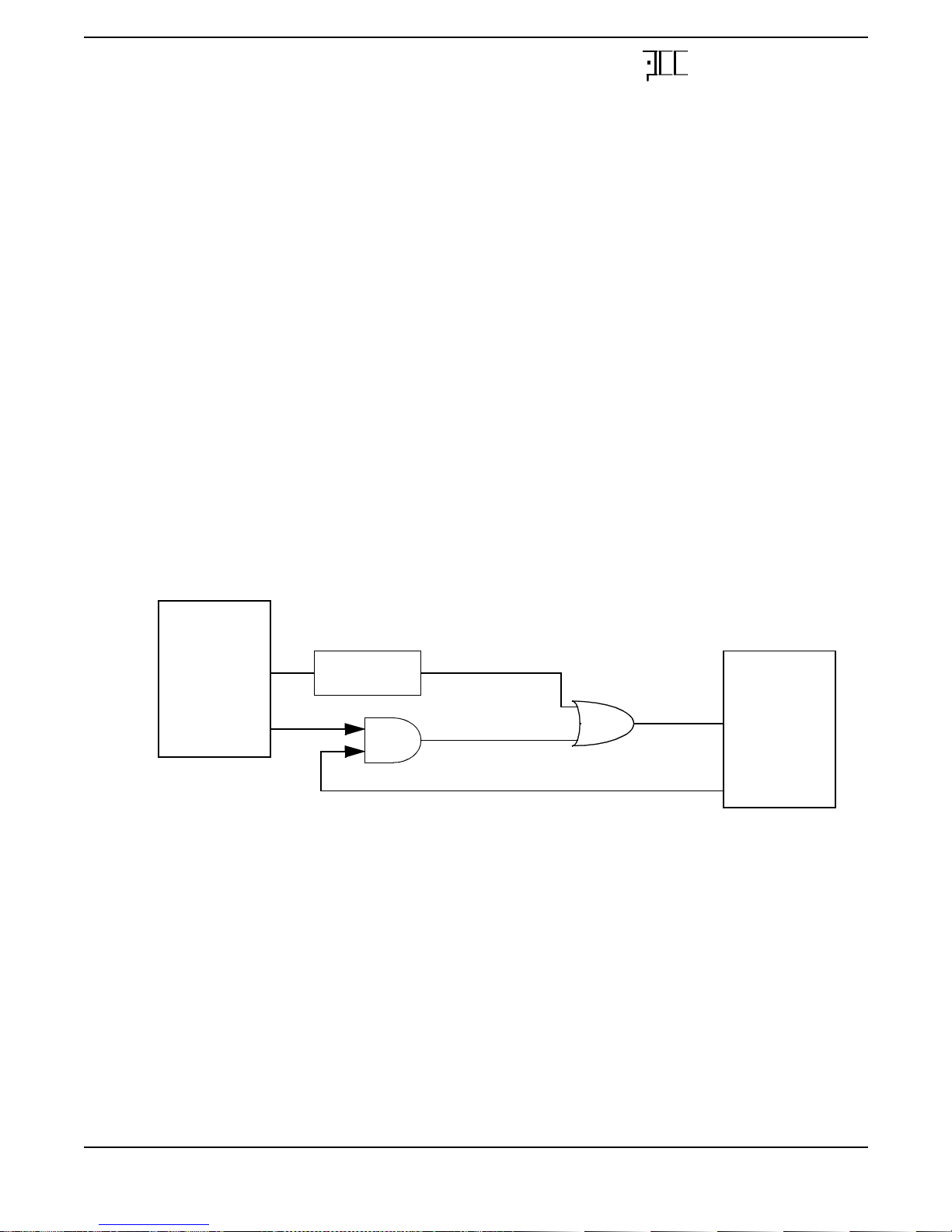
Performance Computer
SCV64 VME Event
This interrupt indicates that an event related to VMEbus use has occurred - such as DMA
has finished or a bus error (SCV64 [-KBER] or VMEbus [BERR*]) has occurred. It is
negated when the appropriate flags in the SCV64 status register are cleared.
The interrupt is enabled by setting the L1E bit in the SCV64 Local Interrupt Enable
Register. The current state of this signal can be read in the LI1 status bit of the SCV64 Local
Interrupt Status Register. The interrupt request level pres ented to the 68060 is determi ned
by 1L2, 1L1, and 1 L0 co nt ro l bits in the SCV64 Local Int err upt s 1 and 0 Control Register.
The SCV64 -VMEINT outp ut dri ves the SCV64 interru pt i nput p in - LIRQ1 t hrough signal
line [-INTP<1>].
Timer Event
The outputs of the Tick Timer and three Interval Timers are OR’ed together generating a
single interrupt to the CPU. This interrupt indicates that a Timer period has expired.
The Timer Event interrupt is enabled by setting the L2E bit in the SCV64 Local Interrupt
Enable Register. The current state of this signal can be read in the LI2 status bit of the
SCV64 Local Interrupt Status Register. The interrupt request level presented to the 68060
is determined by 2L2, 2L1, and 2L0 control bits in the SCV64 Local Interrupts 3 and 2
Control Register.
System Control
Register 2
EITI
ETTI
Figure 12: Timer Block Diagram
Interval Timer
Interval Timers
The SCV64 interrupt input i s dr i ven by the log i cal OR of the SCV64 TICK ou tput and the
82C54 interrupt output. System Status Register 3 identifies the source of the Timer Event.
After reset, the Tick Timer interrupts are enabled and the Interval Timer interrupts are
disabled to maintain compatibility wit h PT-VME151.
Interrupt Request
Tick Timer
Interrupt Request
Timer Event
SCV64
LIRQ2
TICK
Tick
The output of the Tick Timer is neg ated by clearing the CLRTIK control bit in th e
SCV64 Status Register 0.
Interrupts from the Tick Timer can be disabled by clearing the ETTI bit (6) in System
Control Register 2. See “Tick Timer” on page 38 for more information.
Extensible Single Board Computer/Controller User’s Manual 41
Page 56

Section
3
FUNCTIONAL DESCRIPTION
Interval
I/O Event
This input to the SCV64 is the logical OR of the Fast SCSI Processor Chip (FAS216) Interrupt Request and the EPAK Interrupt Request.
FAS216 Requests
The latched outputs of the individual Interval Timers may be cleared by writing the
appropriate bit combinations to the RITI field of System Control Register 2.
Interrupts from the three Interval Timers can be disabled by clearing the EITI bit (5)
in System Control Register 2. See the section “Interval Timer” on page32.
This interrupt indicates that an event related to the FAS216 operation has occurred such as a SCSI state sequence has completed. It is negated by a hardware or software
reset to the FAS216 or a read from the FAS216 Interrupt Register.
The FAS216 does not provide a single mechanism (or bit) to disable all interrupt
requests. Individual interrupt sources can be controlled within the chip, see the
FAS216 documentation for more information. The current state of FAS216 Interrupt
Request signal (INT) can be read in the INT status bit of the FAS216 Status Register.
EPAK Requests (-EPIRQ)
The EPAK module can request 68060 interrupt service. It is typically used by EPAK
devices that do not support vectored interrupt requests. It is negated when the appropriate flags in the EPAK module are cleared.
The ability to disable or check the state of this in terrupt request is a function of the
EPAK module design.
The interrupt is enabled by setting the L3E bit in the SCV64 Local Interrupt Enable
Register. The current state of this signal can be read in the LI3 status bit of the SCV64 Local
Interrupt Status Register. The interrupt request level pres ented to the 68060 is determi ned
by 3L2, 3L1, and 3 L0 co nt ro l bits in the SCV64 Local Int err upt s 3 and 2 Control Register.
The SCV64 interrupt input is driven by the FAS216 INT or the EPAK EPIRQ signal. The
FAS216 INT [-SCINT] or the EPAK [-EPIRQ] signals drive the SCV64 interru pt input pin
-LIRQ3 through signal line [-INTP<3>].
EPAK Vectored Interrupt Request
This interrupt is driven by the EPAK Vectored Interrupt Request signal [-EPVIR]. When
the 68060 acknowledges the interrupt the SCV64 asserts EPAK Vectored Interrupt
Acknowledge (-EPVIA) back to the EPAK m odule. The interrupt request is negated automatically by logic on the EPAK that responds to the interrupt acknowledge (-EPVIA)
generated by the SCV64.
The interrupt is enabled by setting the L4E bit in the SCV64 Local Interrupt Enable
Register. The current state of this signal can be read in the LI4 status bit of the SCV64 Local
Interrupt Status Register. The interrupt request level pres ented to the 68060 is determi ned
by 4L2, 4L1, and 4 L0 co nt ro l bits in the SCV64 Local Int err upt s 5 and 4 Control Register.
42 Extensible Single Board Computer/Controller User’s Manual
Page 57

!
Performance Computer
The 4AV bit in the SCV64 Local Interrupts 5 and 4 C ontrol Register det ermines whether a
“vectored” or “auto-vectored” interrupt is presented to the 68060. The EPAK [-EPVIR]
signal drives the SCV64 interrupt input pin -LIRQ4 through signal line [-INTP<4>].
CAUTION: Due to the PT-VME161 hardware implementation the “vectored” option must
always be used for the SCV64 Local Interrupts 5 and 4 Control Register 4AV bit.
DUART Interrupt Request (-INTP<5>)
This interrupt is driven by the DUART Interrupt Request signal. When the 68060 acknowledges the interrupt the SCV64 asserts an interrupt acknowledge (-INTA<5>) back to the
DUART. The interrupt request is negated by servicing the appropriate interrupt source in
the DUART.
The interrupt is enabled by setting the L5E bit in the SCV64 Local Interrupt Enable
Register. The current state of this signal can be read in the LI5 status bit of the SCV64 Local
Interrupt Status Register. The interrupt request level pres ented to the 68060 is determi ned
by 5L2, 5L1, and 5 L0 co nt ro l bits in the SCV64 Local Int err upt s 5 and 4 Control Register.
The 5AV bit in the SCV64 Local Interrupts 5 and 4 C ontrol Register det ermines whether a
“vectored” or “auto-vectored” interrupt is presented to the 68060. The DUART IRQ pin
drives the SCV64 interrupt input pin -LIRQ5 through signal line [-INTP<5>].
!
CAUTION: Due to the PT-VME161 hardware implementation the “vectored” option must
always be used for the SCV64 Local Interrupts 5 and 4 Control Register 5AV bit.
VMEbus Interrupts
The VMEbus interrupts map directly onto the 68060 CPU interrupt levels. Each has its own
enable bit and each is always vectored. All VMEbus interrupts are level sensitive and not
latched, nor can their status be directly determined, with the exception or IRQ1*. See the
SCV64 User’s Manual for more information on this exception.
The SCV64 VMEbus Interrupt Enable Register allows the individual interrupt request levels to
be enabled or disabled.
Interrupt Acknowledgment
The SCV64 interrupt handler generates the acknowledgment signals during the 68060 IACK
cycle to: auto-vector the cycle, indicate to Local In terrupt level 5 and 4 requesters that they must
supply a vector, or requests the SCV64 to obtain the VMEbus for a VMEbus interru pt acknowledge cycle.
The order of priorities within an y given interrupt request level is auto-vector first, fo llowed by
Local Interrupt level 5 and 4 and finally VMEbus.
VMEbus Requester
Several request and release modes can be selected via the SCV64 Requester Control Register.
The bus release options include: Bus Clear [BCLR*], VMEbus ownership timer, and Release
on Request (ROR) or Release when Done (RWD).
Extensible Single Board Computer/Controller User’s Manual 43
Page 58

Section
3
FUNCTIONAL DESCRIPTION
System Monitor Functions
The SCV64 is capable of providing VMEbus System Controller functions. These include Bus
Arbitration, System Clock Driver, IACK Daisy Chain Dr iver and Bus Timer. The PT-VME161
does not generate the AC Failure detection feature of the VMEbus Power Monitor [ACFAIL*]
however, it is capable of monitoring the sig nal. The VMEbus Serial Clock Driv er f unction s are
not provided.
The SCV64 samples the VMEbus signal [BG3IN*] shortly after the PT-VME161 detects a
power on condition and on every negatin g edge of VMEbus [SYS RST*]. If [BG3IN*] is lo w,
the SCV64 enables itself as the VMEbus System C ontroller. The Sy stem Controller fun ctions
will be enabled automatically if the PT-VME161 is in slot 1 and [BG3IN*] is open. Software
can determine if this has occurred by reading the SYSC status bit of the SCV64 Status Register
1.
CAUTION: The PT-VME161 requires that the card preceding in the bus grant daisy chain
!
adhere to the IEEE 1014 (VMEbus) rule that requires all Bus Grant outputs to be driven high
during reset. If the preceding card is driving [BG3OUT*] low at the end of reset, a system
malfunction could result.
Reset
The VMEbus [SYSRST*] signal can always be driven by the SCV64, whether or not it is
the System Controller. There are three condition s under which [SYSRST*] is driven: the
PT-VME161 detects a power on conditio n, VM Ebus [BG0IN*] is asse rted (while Sys tem
Controller), or software sets the SWRST bit in the SCV64 Gen e ral Control Register.
System Clock Driver
If the PT-VME161 is the System Controller the 16 MHz, 50% duty cycle [SYSCLK] signal
will be generated on the VMEbus.
VMEbus Arbiter
Only enabled when the PT-VME161 is the System Controller, the VMEbus Arbiter
provides four programmable arbitration schemes along wi th arbitration time-out.
The arbitration mode is determined by the ARB1 and ARB0 bits in the SCV64 VMEbus
Arbiter Register. The possible modes are: Full Round Robin. Bus Request Level 3 has
priority over levels 2, 1, and 0 which are handled in Round Robin mode. Bus Request
Levels 3 and 2 have priority over levels 1 and 0 which are handled in Round Robin mode.
And, full Priority mode.
Arbitration time-out is enabled by th e ATEN bit in the SC V64 VMEb us Arbit er Re gister.
The Bus Grant issued by the arbiter will be withdrawn after 16 us, if no card asserts BBSY*
to take ownership of the VMEbus. Th e arbiter then waits 16 us to allow the deasserted grant
to fully propagate through the daisy chain, then rearbitrates the bus.
IACK Daisy Chain Driver
The IACK Daisy Chain Driver (DCD) performs the standard VMEbus System Controller
IACK DCD function, as well as providing the VMEbus Interrupt Gen e rator logic.
44 Extensible Single Board Computer/Controller User’s Manual
Page 59

I/O UTILITIES
Performance Computer
Bus Timer
The SCV64 as System Controller provides VMEbus Data Transfer Time-out functionality.
VMEbus data transfers are terminated with the error signal BERR*, if a slave does not
respond within a programmed time. The time-out period may be 16, 32, or 64 us, or
“never”. The default value after reset is 64 us. The VXL1 and VXL0 control bits in the
SCV64 VMEbus Arbiter Register determine the time-out perio d.
System Control Registers
The System Control Registers provide the PT-VME161 with miscellaneous control functions not
provided in other registers. They are all 8-bit, read/write registers.
These registers can be read back. This allows the use of AND or OR instructions to clear and set individual bits.
!
CAUTION: These registers should only be referenced using byte operations! Reading any of them as a
word or longword will be translated into multiple byte reads by the sizing logic, with the same data byte
being repeated on each reference. Writing them as a word or longword can cause problems because the
bus sizing forces multiple byte writes to occur. This will leave only the last (most significant) byte in the
selected register. The other bytes w ill have previously been pumped through the register and if they are
not identical to the MSB the respective bits of the control register will toggle.
System Control Register 1
System Control Register 1 is an 8-bit, read/write register. All bits are cleared to zero (0) by Local
Reset. It resides at location 0D000000h.
VMEbus Page Select
Access to the VMEbus address space is through the local addresses 80000000h-FFFFFFFFh. In
order to Access the full VMEbus address space, the VMEbus Page Select bit (VPG) in the
System Control Register is used to define VMEbus address bit 31. When the VMEbus Page
Select bit is 0, PT-VME161 addresses 80000000h-FFFFFFFFh are mapped to VMEbus
addresses 00000000h - 7FFFFFFFh. When the VMEbus Page Select bit is 1, PT-VME161
addresses 80000000h-FFFFFFFFh are mapped to VMEbus addresses 80000000h-FFFFFFFFh.
Local Reset clears (0) this bit.
User LEDs
There are four LEDs on the front panel (D3, D2, D1, and D0) that are under program control.
Writing a one to the LED3-LED0 bits in the Sy stem Co ntrol Regis ter will ligh t the respective
LED. When Local Reset is asserted all the four LEDs will be turned off.
Extensible Single Board Computer/Controller User’s Manual 45
Page 60
Section
3
FUNCTIONAL DESCRIPTION
SCSI DMA Read/Write Direction
SDIR in the System Control Register determines the direction of a data transfer during a SCSI
DMA operation. Setting this bit will gene rate data movement from DRAM to the FAS216, a
write to the SCSI bus. Clearing it moves data from the FAS216 to DRAM, a read from the SCSI
bus. Local Reset clears (0) this bit (SCSI DMA Read).
EPAK Space Cache Enable
The ability to cache information in the EPAK address space (30000000h-3FFFFFFFh) is determined by the MC68060 Transparent Translation Registers. This makes the Enable EPAK
Caching bit of the Control Register irrelevant. Below are the possible combinations of events:
Table 1: EPAK Caching Options
68060 DTTR
EPAK Cache Enable
Disabled Don’t Care No (Normal mode)
Enabled True Yes
Enabled False N o, but 4 lwords fetched
Local Reset clears (0) this bit, enabling caching. See “APPENDIX H: PT-VME151A Differences From VME131/141” on page 94 for an in-depth discussion of EPAK caching.
VME151 Control Register
EPAK Cache Enable
EPAK Caching?
VMEbus Space Cache Enable
Reads from the VMEbus address (80000000h-FFFFFFFFh) space can be cached. When the
VCE bit in the System Control Register is cleared (0) VMEb us space caching is enabled. When
set (1) it is disabled. Local Reset clears (0) this bit, enabling caching.
The VCE bit is intended to enable or disable VMEbus caching. The Transparent Translation
Registers of the 68060 disable VMEbus caching by default, making the VCE bit of the System
Control Register One irrelevant. If the Transparent Translation Registers are used to enable
VMEbus caching, then the VCE bit must be set to 0 with a write operations to enable caching.
This feater provides backward compatability with the VME131/141/151/151A.
NOTE: If the VMEbus Page Select bit is toggled while caching is enabled a system failure could
result!
System Control Register 2
System Control Register 2 is an 8-bit, read/write register. All bits except ETTI are cleared to zero
(0) by Local Reset. ETTI is set to 1 by Local Reset. This register resides at location 50000000h.
Enable EPAK Access from the VMEbus
The EPAK expansion module can be Accessed by a VMEbus master as part of the PT-VME161
slave image when the EEAV bit is 0, the VMEbus address bit 24 is 1, and the A32SIZ field of
the DARF VMEBAR register is programmed to allow a A32 Slave Image Size greater than or
equal to 32MBytes (Dh). In this case a portion of the PT-VME161 slave image is replaced by
46 Extensible Single Board Computer/Controller User’s Manual
Page 61

Performance Computer
the EPAK’s address space. When EPAK Accesses from the VMEbus are disabled, all of the
PT-VME161 installed DRAM may be Accessed by a VMEbus master. EEAV is cleared at reset,
enable EPAK Access. EEAV is register bit 0.
Enable Parity Error Checking
Parity generation and checking is available for the 16M, 32M, and 64M DRAM configurations.
When EPEC is 1, parity checking is enabled for all DRAM reads. Parity errors detected during
68060 or EPAK DRAM reads will return a Bu s Error to the respective device. Parity errors
detected during SCSI DMA transfers or SCV64 Local Bus Master cycles will result in an interrupt request on the SCV64’s L7IMEM input. The source of the error may be determined by
reading System Status Register 2. See “System Status Register 2” on page 49.
Parity is generated and stored on all DRAM write cycles, regardless of the state of EPEC. If
parity is not available (4 M or 8M configurati ons), pari ty checking is di sabled and EPE C will be
ignored. Reset clears EPEC, disabling parity checking.
NOTE: EPEC should never be set while EBP is set. See “Enable Bad Parity” below.
EPEC is register bit 1.
Enable Bad Parity
For testing purposes it may be desirable to force parity errors. When EBP is 1, the parity bit
written to DRAM with the data is complemented, generating faul ty parity. Subsequent read
cycles from the same address will generate parity errors until good pa rity is written.
NOTE: EBP should never be set while EPEC is set. Otherwise each DRAM write will generate
a parity error.
It should be kept in mind that the 68060 may reorder a sequence of reads and writes in a code
segment. NOPs should be placed in the instruction stream to eliminate the effect. The code
segment to write bad parity should be as follows:
NOP
move.b #$04,$50000000 ;Set EBP and clear EPEC
NOP
[Move data with bad parity to DRAM addresses]
NOP
move.b #$02,$50000000 ;Clear EBP and Set EPEC
EBP is always cleared at reset allowing good parity to be written. EBP is regis ter bit 2 .
Extensible Single Board Computer/Controller User’s Manual 47
Page 62

Section
3
FUNCTIONAL DESCRIPTION
Reset Interval Timer Interrupts
The RITI bits are encoded to reset the Request Latch of the individual Interval Timers. When
an Interval Timer reaches it’s terminal count, the event is recorded by its Request Latch. The
outputs of the three Request Latches are OR’ed together, generating the Interval Timer Interrupt
Request to the 68060. The interrupt request from an individual Interval Timer remains active
until its Request Latch is reset using this field.
Value Function
3 Reset Interval Timer 2 Request Latch
2 Reset Interval Timer 1 Request Latch
1 Reset Interval Timer 0 Request Latch
0 No action
RITI is a two bit field. It consists of register bits 3 and 4, where bit 3 is the least significant bit.
This field is always read as 0.
Enable Interval Timer Interrupts
All interrupt requests from the three Interval Timers can disabled. When the EITI bit in System
Control Register 2 is cleared (0) Interval Timer interrupt requests are disabled. When set (1)
they are enabled. Local Reset clears (0) this bi t, disabling Interval Timer interrupts. EITI is
register bit 5.
Enable Tick Timer Interrupts
Interrupt requests from the SCV64 Tick Timer can disabled. When the ETTI bit in System
Control Register 2 is cleared (0) Tick Timer interrupt requests are disabled. When set (1) they
are enabled. Local Reset sets (1) this bit, enabling Tick Timer interrupts. ETTI is register bit 6.
Enable Bus Snooping
Bus snooping allows invalidation of 68060 cache entries when DRAM is written by a bus
master other than the 68060. Without snoopi ng , DMA operatio ns can updat e DRAM while the
68060 retains old data in its internal caches.
Note: When bus snooping is enabled, the SCV64 DMA burst cycle length must be set ot 4 for
proper operation.
Snooping is disabled after a reset.
48 Extensible Single Board Computer/Controller User’s Manual
Page 63

Performance Computer
System Status Registers
The System Status regis ter provides the PT -VME161 with status i nformation not pr ovided in oth er registers. It is a read only register. All unused bits (31-4) should be masked to zero (0) for future exp ansion.
This register should only be referenced using byte operations. Reading it as a word or longword will be
translated into multiple byte reads by the sizing logic, with the same data byte being repeated on each
reference.
System Status Register 1
System Status Regist er 1 is an 8-bi t, r ead only regi ster. This regi ster resi des at locatio n 0C 000000 h.
Hex Switch
The current setting of the front panel hexadecimal switch can be read through this register. The
hex switch value will be presented as a nibble on data bits 3-0 at locati on 0C000 000h (bit 0 is
the least significant bit). This four bit field is referred to as HSW.
System Status Register 2
System Status Register 2 is an 8-bi t, read o nly regi s t er. This regi s ter r esi d es at locat io n 60 000000h.
68060 Parity Error
When the 68060 Parity Error bit (named 060 PE) is r ead as 1, it in dicates that a parity error was
detected during a 68060 DRAM read cycle. Notification of the er ror is thr ough a Bus Erro r that
is generated as a acknowledgment on th e DRAM ref erence. Th e B us E rror Han dler must ch eck
this bit to determine if bad DRAM pa rity was the source of the Bus Error. 060PE is cleared by
reset and after each time System Status Register 2 is read. 060PE is register bit 1.
SCSI DMA Parity Error
When the SCSI DMA Parity Error bit (named SDMAPE) is read as 1, it indicates that a parity
error was detected during a SCSI DMA DRAM read cycle. Notification of the error is though a
level 7 Interrupt to the 68060 that is generated immediately after the DRAM reference in error.
The Level 7 Interrupt Handler must check t his bit to determine if bad DRAM parity was the
source of the interrupt. SDMAPE is cleared by reset and after each time System Status Register
2 is read. SDMAPE is register bit 2.
SCV64 Parity Error
When the SCV64 Parity Error bit (named SCV64PE) is read as 1, it indicates that a parity error
was detected during a SCV64 DRAM read cycle. Notification of the error is though a level 7
Interrupt to the 68060 that is generated immediately after the SCV64 reference in error. The
Level 7 Interrupt Handler must check this bit to determine if bad SCV64 parity was the source
of the interrupt. SCV64PE is cleared by reset and after each time System Status Register 2 is
read. SCV64PE is register bit 3.
Extensible Single Board Computer/Controller User’s Manual 49
Page 64

Section
3
FUNCTIONAL DESCRIPTION
EPAK Parity Error
When the EPAK Parity Error bit (named EPAKPE) is read as 1, it indicates that a parity error
was detected during a DRAM read cycle by an EPAK master. Notification of the error is though
a Bus Error that is generated as a acknowledgment to the EPAK module on the DRAM reference. The Bus Error Handler for the EPAK must check this bit to determine if bad DRAM parity
was the source of the Bus Error. EPAKPE is cleared by reset and after each time System Status
Register 2 is read. EPAKPE is register bit 4.
SCSI Present
When the SCSI Present bit (named SCSIP) is read as 1, it indicates that the SCSI controller and
associated logic is installed. SCSIP is register bit 5.
System Status Register 3
System Status Register 3 is an 8-bi t, read o nly regi s t er. This regi s ter r esi d es at locat io n 68 000000h.
DRAM Size
The DRAM Size field (named DRAMSZ) indicates the size of the DRAM module installed on
the PT-VME161 base board. DRAMSZ is a three bit field. It consists of register bits 0 through
2, where bit 0 is the least significant bit. The following table elaborates the possible values:
Value DRAM Size
7-5 Reserved
4 64 Meg
3 32 Meg
2 16 Meg
1 8 Meg
0 4 Meg
Parity Installed
If equal to 1, the Parity Installed bit (named PARI) indicates parity logic and me mory is populated on the DRAM module. PARI is register bit 3.
Interval Timer Interrupt Pending
The ITIP bits reflect the state of the respective Interval Timer Request Latch. When set (1) the
bit indicates that the Interval Timer’s OUTPUT pin has been asserted. These bits wi ll remain
set until explicitly reset using the RITI field in System Control Register 2. After Local Reset all
ITIP bits will be cleared (0). ITIP0, ITIP1, and ITIP2 correspond to register bits 4, 5, and 6,
respectively.
50 Extensible Single Board Computer/Controller User’s Manual
Page 65

Performance Computer
DUART
The Motorola Dual Asynchronous Receiver/Transmitter (MC68681 DUART) provides a General
Purpose Timer, Parallel Input and Output Ports, besides the dual Serial Port capability.
Utility Serial Ports
The DUART provides two general purpose asynchronous serial ports. Port “A” is equipped with
basic modem controls: DTR, DSR, RTS, CTS. Port “B” is transmit and receive data only. Both ports
are equipped with RS-232 line drivers and receivers. The baud rate for each port can be set independently over the common asynchronous speed ran ge (5 0 to 38.4K baud). The ports can be controlled
via interrupts or polled I/O.
If you recieved a Performance Computer Debugger (PTBUG) as part of your order, Port A of the
DUART will be set to 9600 baud, 1 stop bit, no parity. PTBUG ignores CTS and DTR and deasserts
RTS and DSR (false).
The Utility Serial Port interconnect is located on the front panel and uses a 14-pin dual row pin
header connector.
General Purpose Timer/Counter
The General Purpose Timer is a flexible user programmable 16-bit counter/timer. The clock source
of the timer is derived from the 3.6864 MHz crystal attached to the DUART. Parallel Output Port
pin 3 can be programmed as an output of the timer allowing EPAK boards to take advantage of this
timer function through the [+EPKIO] signal.
DUART parallel Input Port pin 2 is unconnected, therefore the “External (IP2)” clock sources identified in the Counter/Timer Mode and Source Select field of the DUART Auxiliary Control Register
(ACR[6:4]) are not valid choices.
This timer is used by OS-9 for its real-time clock. For detailed information on the DUART and the
General Purpose Timer/Counter refer to the MC68681 Multi-Function Peripheral Specification.
Parallel Input Port
Clear-to-Send
Parallel Input 0 of the DUART is attached to the RS-232 Clear-to-Send (CTS) receiver for
Serial Port “A”. To allow CTS to act as a hardware enable for the transmitter, CTS Enable
Transmitter bit (4) in DUART Channel A Mode Register must be set to 1. The state of this
control signal can be read from IP0 bit (0) of the DUART Input Port Register.
Data-Terminal-Ready
Parallel Input 1 of the DUART is attached to the RS-232 Data-Terminal-Ready ( DTR) receiver
for Serial Port “A”. The state of this control signal can be read from the IP1 bit (1) of the
DUART Input Port Register.
The DUART is capable of generating an interrupt to the 68060 if a change of state occurs on
this signal. To accomplish this, the Delta IP1 IRQ bit (1) of the DUART Auxiliary Control
Register must be set and the SCV64 registers associated with the DUART Interrupt Request
must be setup.
Extensible Single Board Computer/Controller User’s Manual 51
Page 66

Section
3
FUNCTIONAL DESCRIPTION
EPAK General Purpose Input
Parallel Input 3 of the DUART is attached to the EPAK +EPKIO signal. The state of this control
signal can be read from the IP3 bit (3) of the DUART Input Port Register. The function of this
pin is determined by the attached EPAK Expansion Module.
The DUART is capable of generating an interrupt to the 68060 if a change of state occurs on
this signal. To accomplish this, the Delta IP3 IRQ bit (3) of the DUART Auxiliary Control
Register must be set, and the SCV64 registers associated with the DUART Interrupt Request
must be setup.
Serial EEPROM Data In
Parallel Input 5 of the DUART is attached to the Data Out (DO) pin of the 93C46 Serial
EEPROM. The state of this control signal can b e read f rom the IP5 bit (5) of the DUART Input
Port Register.
Parallel Output Port
Request-to-Send
Parallel Output 0 of the DUART is attached to the RS -232 Req uest-to-Send (RTS) transm itter
for Serial Port “A”. To allow RTS to act as a hardware indicator that the channel A transmit
FIFO has data ready to send, Tx RTS Control bit (5) in DUART Channel A Mode Register must
be set to 1. Programmed I/O can control the state of this signal with the OPR0 bit (0) of the
DUART Output Port Register.
Data-Set-Ready
Parallel Output 1 of the DUART is attached to the RS-232 Data- Set-Ready (DSR) transmitter
for Serial Port “A”. Programmed I/O can control the state of this signal with OPR1 bit (1 ) of the
DUART Output Port Register.
EPAK General Purpose Output
Parallel Output 3 of the DUART is attached to the EPAK +EPKIO signal. The state of this
control signal can be controlled by the OPR3 bit (3) of the DUART Output Port Register. The
function of this pin is determined by the attached EPAK Expansion Module.
Serial EEPROM Select
Parallel Output 5 of the DUART is attached to the Chip Select (CS) pin of the 93C46 Serial
EEPROM. Programmed I/O can control the state of this signal with the OPR5 bit (5) of the
DUART Output Port Register.
Serial EEPROM Control
Parallel Output 6 of the DUART is attached to the Control (SK) pin of the 93C46 Serial
EEPROM. Programmed I/O can control the state of this signal with the OPR6 bit (6) of the
DUART Output Port Register.
52 Extensible Single Board Computer/Controller User’s Manual
Page 67

Performance Computer
Serial EEPROM Data Out
Parallel Output 7 of the DUART is attached to the Data In (DI) pin of the 93C46 Serial
EEPROM. Programmed I/O can control the state of this signal with OPR7 bit (7) of the DUART
Output Port Register.
Extensible Single Board Computer/Controller User’s Manual 53
Page 68

3
Section
FUNCTIONAL DESCRIPTION
SCSI Controller
The Emulex FAS126 Fast SCSI Processor Chip is a high performance CMOS device that conforms to
the ANSI standards, X3.131-19 86 (S CS I-1 ) and X3T9 .2/86 -10 9 R ev.10c (SCSI-2), for Small Computer
Systems Interface (SCSI). An 8-bit bus provides FAS216 register Access to the 68060. The FAS216’s
internal sequencer is capable of performing common SCSI algorithms, or sequences, in response to a
single command, thus reducing the SCSIbus protocol overhead.
The FAS216 uses a register superset of the NCR 53C94 used on the PT-VME131 to provide SCSI-2
functionality. This compatibility offers the user an easy upgrade to SCSI-2 performance.
The FAS216 is permanently strapped in Bus Configuration Mode 2 (dual bus, multiplexed, byte control,
16-bit DMA transfers). Also, because of the hardware implementation, the “Alternate DMA mode”
option in FAS216 Configuration Register 3 must not be enabled.
The FAS216 is driven with a 40 MHz (25 ns.) clock. Various programmable parameters derive their
timing from this clock.
SCSI Bus
The FAS216 incorporates on-chip 48 mA drivers for single-ended (TTL) transmission. It is capable of
operating at a sustained data transfer rate of up to 5 megabytes per second (SCSI-1) and 10 megabytes
per second (SCSI-2) synch ronous modes or 7 megaby tes per second in asynchr onous mode. Parity gen eration and checking is optional on all SCSI bus transfers.
The SCSI interface is through the P2 VME connector. Termination is provided by optional plug-in
resistor packs. The resistor packs should be installed if the PT-VME1 61 is at either end of a SCSI cable.
Conversely, the resistor packs should be removed if the PT-VME161 is installed in the middle of the
SCSI cable.
The local SCSI termination circuit draws its power from the SCSI TERMPWR signal [TPWR]. Jumper
K6 determines whether the PT-VME161 sources SCSI TERMPWR [TPWR] (pins 1-2 shunted) or not
(pins 1-2 open).
A 1 amp fuse (Littelfuse 273-001) protects the S CSI termination power [TPWR] from short circuit con ditions.
For more information see “ SCSI Termination” on page 17 and “ SCSI Considerations” on page23.
Register Access
The sixteen internal r egister locati ons of the FAS21 6 reside at locatio ns 0A000000h t hrough 0A0000 0Fh
in the 68060’s address space. They are accessed through the 8-bit Buffered Data/Address bus attached to
bits <24:31> of the Microprocessor Data Bus. The PT-VME161 incorporates logic that invokes the
dynamic bus sizing mechanism of the 68060 forcing byte operations on any size reference to the 8-bit
Buffered Data/Address Bus.
54 Extensible Single Board Computer/Controller User’s Manual
Page 69

Performance Computer
DMA Mechanism
SCSI data phase bytes can be transferred with Direct Memory Access of the PT-VME161. Under
program control the following steps must be perform ed to initiate a SCSI DMA transfer:
The SCSI Memory Address Register must be loaded with the source/destination address for the
transfer.
The System Control Register, SCSI DMA Read/Write Direction (SCDRD) bit is written to indicate
to the PT-VME161 control logic the direction of the transfer.
The FAS216 Transfer Count register is loaded with the desired size of the transfer (up to 64 KBytes).
Issue a data transfer command to the FAS216.
The hardware will handle the data transfer between the FAS216 and local DRAM.
Parity is generated and checked by PT-VME161 hardware on local DRAM Accesses during SCSI DMA.
A level 7 interrrupt may be generated if a parity error is detected. See “Parity” on page 30 for more information.
Interrupts
The 68060 can be notified of the completion of an operation of a change in state through the interrupt
mechanism provided on the FAS216 and SCV64. The FAS216 Interrupt Register, in conjunction with
the FAS216 Status and FAS216 Sequence Step registers, are used to determine the source of an FAS216
interrup t.
For FAS216 interrupts to be forwarded to the 68060 the SCV64 the interrupt mechanism must be enabled
by setting the L3E bit in the SCV64 Local Interrupt Enable Register. The current state of this signal can
be read in the LI3 status bit of the SCV64 Local Interrupt Status Register. See the VMEbus Interface,
SCV64, General Purpose Local Interrupts, I/O Event, FAS216 Requests s ection abov e for fur ther info rmation.
NOTE: The SCV64 General Purpose Local Interrupt input is driven by the FAS216 INT or the EPAK
EPIRQ signal!
A second interrupt mechanism exists that allows the detection of a RESET condition on the SCSIbus. A
Level 7 L7IMEM interrupt can be generated in the SCV64. The interrupt is enabled by setting the
MEMIS bit in the SCV64 Level 7 Interrupt Status Register. The current state of this signal can be read
in the MEMIP status bit of the SCV64 Status Register 0. See VMEbus Interface, SCV64, Interrupt
Handler, Local Level 7 Sources section above.
See the FAS216 Technical Manual for more information on the Fast SCSI Processor Chip.
Termination
Fuse F1 (Littelfuse Part No. 273-001) provides short circuit protection for TERMPWR . To remove the
fuse, place the PT-VME161 on a work surface component side up with the VMEbus connectors closest
to the observer. Grip the clear body of fuse F1 and pull to the right. To replace the fuse reverse the
Extensible Single Board Computer/Controller User’s Manual 55
Page 70

Section
3
FUNCTIONAL DESCRIPTION
process. The bidirectional arrow in “Figure 6: SCSI Components” on page 17 shows the direction of
motion.
See “TERMPWR Overview” on page 17 for a discussion of the uses of TERMPWR.
56 Extensible Single Board Computer/Controller User’s Manual
Page 71

EPAK Interface
The Performance Technologies family of Single Board Controllers features provisions for user defined
expansion modules. Two basic expansion module strategies are available. The “EPAK” is a 3" x 9"
mezzanine board which is intended for applications that must be limited to a sin gle slot. The “EBOARD”
is a full-sized VMEbu s 6U module which requir es the use of a second slo t . EB OARDs may be designed
with or without backplane Access.
The interface between the PT-VME161 and the expansion module is implemented using three 36-pin
connector strips (referred to in the Expansion Module Design Guide as J1, J2, and J3).
The interface is organized such that simple slave expansion modules need to connect only to the J1
connector, which provides 8 bits of address and data and the co ntrol signals to support this class of slave.
Adding a J2 connector to the expansion module brings the number of address lines up to 24 and the
number of data lines up to 16. Full A32:D32 slave, as well as all m aster expansion mo dules, must use all
three connectors.
Many signals on the expansion module interface are simply extensions of the MC68060 signal of a
similar name (MP prefix). Refer to the Motorola MC68060 User’s Manual for additional information on
the behavior of these signals. Other signals are annotated as “Expansion” (EP prefix) and are uniquely
defined for this application.
Performance Computer
The PT-VME161 partitions the expansion module (EPAK) memory space into two regions: the first
requires that the expansion module generate Data Size Acknowledgments (-EPSA0,1) to accommodate
the timing delay of the selected expansion module slave device, the second region requires no response
signal from the expansion module ([-EPSA0] and [-EPSA1] need not be driven). The second region
allows zero wait state Access to SRAM or registers on an EPAK.
The EPAK may be Accessed form the VMEbus as part of the PT-VME161 address space. To do so,
VMEbus address bit A24 must be 1, the EEAV bit in System Control Register 2 must be 0, and the
A32SIZ field of the DARF VMEBAR register must be programmed to allow an A32 Slave Image Size
greater than or equal to 32MBytes (Dh). See “Enable EPAK Access from the VMEbus” on page 46 for
more information.
Parity is generated and checked by PT-VME161 hardware on local DRAM Accesses by EPAK masters.
A Bus Error may be generated as an acknowledgement to a reference if a parity error is detected. See
“Parity” on page 30 for more information.
For more information refer to the Expansion Mo dule Design Guide.
Extensible Single Board Computer/Controller User’s Manual 57
Page 72

Section
3
FUNCTIONAL DESCRIPTION
58 Extensible Single Board Computer/Controller User’s Manual
Page 73

Section
4
Memory Map
FUNCTIONAL SUMMARY
Table 2 describes the location of all configuration and operational registers of the PT-VME161 as seen
by the MC68060. The sizing column indicates if the device supports data bus sizing.
Table 2: Memory Map
ADDRESS RANGE DEVICE WIDTH SIZING
00000000h-03FFFFFFh ROM/PROM (U36) BYTE Yes
04000000h-07FFFFFFh ROM/SRAM (U24) BYTE Yes
08000000h-0800000Fh 68681 DUART BYTE Yes
0A000000h-0A00000Fh FAS216 SCSI BYTE Yes
0C000000h Status Register 1 BYTE No
0D000000h Control Register 1 BYTE No
0E000000h SCSI MAR LWORD only No
0F000000h DS1643 RTC BYTE No
10000000h-1000000Fh Unassigned
18000000h-1800004 E0 SCV64 LWORD only No
20000000h-2FFFFFFFh Main Memory LWORD Yes
30000000h-37FFFFFFh EPAK EPAK defined
38000000h-38FFFFFFh EPAK 0 WS LWORD Yes
40000000h-4FFFFFFFh UNASSIGNED
50000000h Control Register 2 BYTE No
60000000h Status Register 2 BYTE No
68000000h Status Register 3 BYTE No
70000000h-70000003h 82C54 Interval Timer BYTE No
80000000h-FFFFFFFFh VMEbus Slave Defined
Extensible Single Board Computer/Controller User’s Manual 59
Page 74
Section
4
FUNCTIONAL SUMMARY
Default VMEbus Slave Addressing
If you received a Performance Computer Debugger (PTBUG) as part of your order, the firmware will
initialize the SCV64 VMEbus Base Address Register (VMEB AR) with the value 0060014Ch and the
SCV64 Access Protect Boundary Register (APBR) with 00000001h. These values will result in the
following address maps as seen by a VMEbus master.
After PTBUG initialization the PT-VME161 will respond to all Standard and Extended, non-privileged
and supervisory, data and program VMEbus accesses. These include 32-bit and 64-bit block transfers.
(Address Modifier codes 38h-3Fh and 08h-0Fh.)
NOTE: Due to the way the SCV64 is initialized by PTBUG, only 4 MB ytes of PT-VME161 address
space is accessible to the VMEbus. So even though Local Reset enables “EPAK access from the
VMEbus” (EEAV in System Control Register 2 = 0), the EPAK address space cannot actually be
accessed by a VMEbus master. The A32SIZ field of the SCV64 VMEBAR register must be reprogrammed to allow an A32 Slave Image Size greater than or equal to 32MBytes (Dh).
Table 3 describes the default address map of the PT-VME161 as seen by a VMEbus master using A24
addressing.
Table 3: Default VMEbus A24 Memory Map
ADDRESS RANGE DEVICE ACCESS
000000h-00FFFFh Local DRAM
(Write Protected)
010000h-3FFFFBh Local DRAM BYTE, WORD, LWORD,
3FFFFCh Location Monitor BYTE, WORD, LWORD
400000h-FFFFFFh UNASSIGNED
Table 4 describes the default address map of the PT-VME161 as seen by a VMEbus master using A32
addressing.
BYTE, WORD, LWORD,
D32 and D64 BLOCK
D32 and D64 BLOCK
Table 4: Default VMEbus A32 Memory Map
ADDRESS RANGE DEVICE ACCESS
00000000h-5FFFFFFFh UNASSIGNED
60000000h-6000FFFFh Local DRAM
(Write Protected)
60010000h-603FFFFBh Local DRAM BYTE, WORD, LWORD,
603FFFFCh Location Monitor BYTE, WORD, LWORD
60400000h-FFFFFFFFh UNASSIGNED
BYTE, WORD, LWORD,
D32 and D64 BLOCK
D32 and D64 BLOCK
NOTE: An attempt to write PT-VME161 “Write Protected” DRAM will result in a Bus Error being
returned to the VMEbus master on the reference.
60 Extensible Single Board Computer/Controller User’s Manual
Page 75
161 System Registers
There are six registers on the PT-VME161 that are not defined in the referenced d ata sheets. These registers are unique to the PT-VME161, providing control of major functional blocks and status.
System Control Register 1
Performance Computer
Address 0D000000h
Byte Read/Write Only
All bits cleared to zero by reset
76543210
VPG
LED0
LED1
LED2
LED3
SDIR
ECE
VCE
Bit Name Function
0 VPG VMEbus Page bit
1 VME address bit 31=1
0 VME address bit 31=0
1 LED0 User Programmable LED D0
1 LED on
0 LED off
2 LED1 User Programmable LED D1
1 LED on
0 LED off
3 LED2 User Programmable LED D2
1 LED on
0 LED off
4 LED3 User Programmable LED D3
1 LED on
0 LED off
5 S DIR SCSI DMA Direction
1 SCSI DMA Write (read from memory)
0 SCSI DMA Read (write to memory)
6 ECE Enable MC68060 caching of EPAK accesses. See “PT-VME151A Control
Register Differences” on page 96 for in-depth discussion.
Not Used.
Extensible Single Board Computer/Controller User’s Manual 61
Page 76

Section
4
FUNCTIONAL SUMMARY
7 VCE Enable 68060 caching of VMEbus accesses. See “PT-VME151A Control
Register Differences” on page 96 for in-depth discussion.
1 Disable caching
0 Enable caching
62 Extensible Single Board Computer/Controller User’s Manual
Page 77
System Control Register 2
Address 50000000h
Byte Read/Write Only
All bits cleared to zero by reset, except ETTI
76543210
EEAV
EPEC
EBP
RITI
EITI
ETTI
ESNP
Bit Name Function
0 EEAV Enable EPAK Access from VMEbus
1 Enable EPAK Access from VMEbus when A24 = 1
0 Disable EPAK Access from VMEbus
Performance Computer
1EPEC
1,2
Enable Parity Error Checking
1 Check for parity errors
0 Do not check for parity errors
2EBP
3
Enable Bad Parity
1 Write bad parity
0 Write normal parity
4-3 RITI
4
Reset Interval Timer Interrupt pending latch
3 Reset Interval Timer 2 Interrupt Pending Latch
2 Reset Interval Timer 1 Interrupt Pending Latch
1 Reset Interval Timer 0 Interrupt Pending Latch
0 No action
5 EITI Enable Interval Timer Interrupts
1 Enable interrupts
0 Disable interrupts
6 ETTI Enable Tick Timer Interrupts
1 Enable interrupts
0 Disable interrupts
7ESNP
5
Enable Bus Snooping
1 Enable Snooping
0 Disable snooping
1
DRAM MUST be initialized before parity checking is enabled.
2
DO NOT enable if EBP = 1.
3
DO NOT enable if EPEC = 1.
4
RITI always read as 0.
5
SCV64 DMA burst cycle length must be set to 4.
Extensible Single Board Computer/Controller User’s Manual 63
Page 78
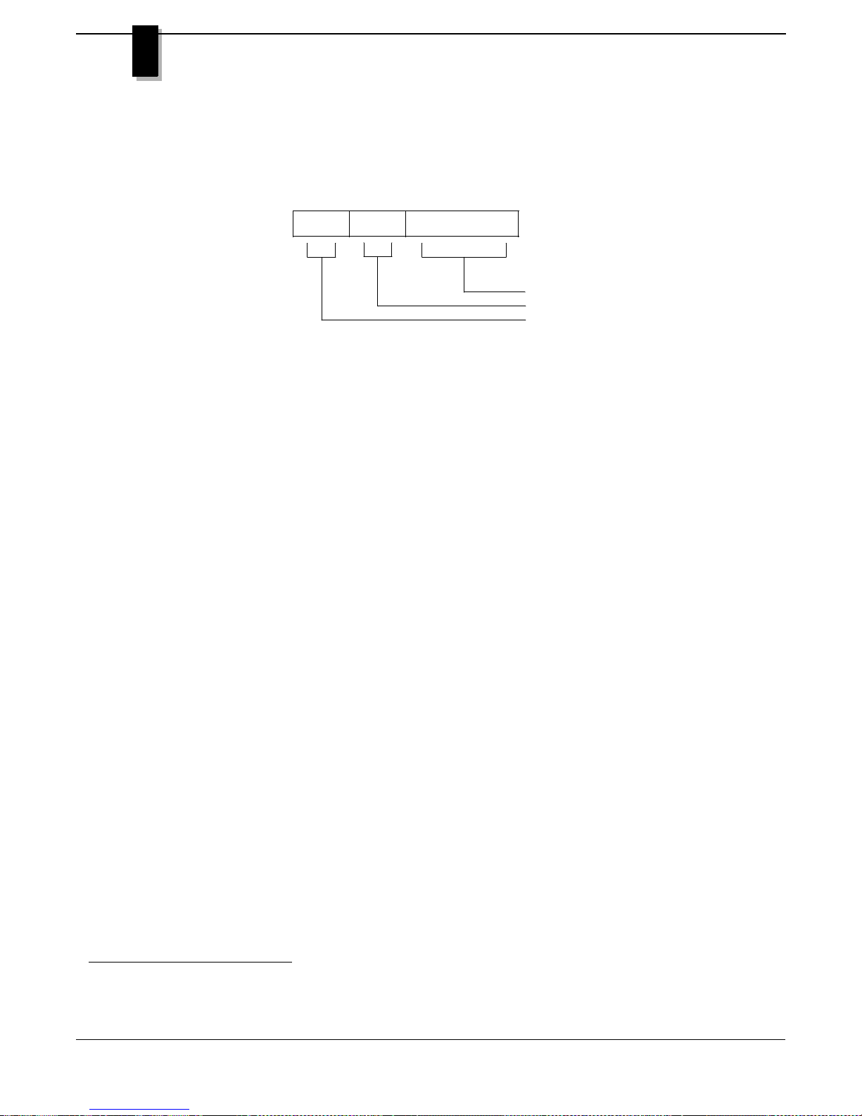
Section
4
FUNCTIONAL SUMMARY
System Status Register 1
Bits Name Function
3-0 HSW Value of Hex Switch
Address 0C000000h
Byte Read Only
76543210
HSW[3-0]
SRSZ[1-0]
Reserved
5-4 SRSZ SRAM Size
0 No SRAM installed
7-6 Reserved, mask to zero when read
6
6
The PT-VME161 does not support SRAM so this field is always read as zero. This provides backwards compatibility with the PT-VME151.
64 Extensible Single Board Computer/Controller User’s Manual
Page 79
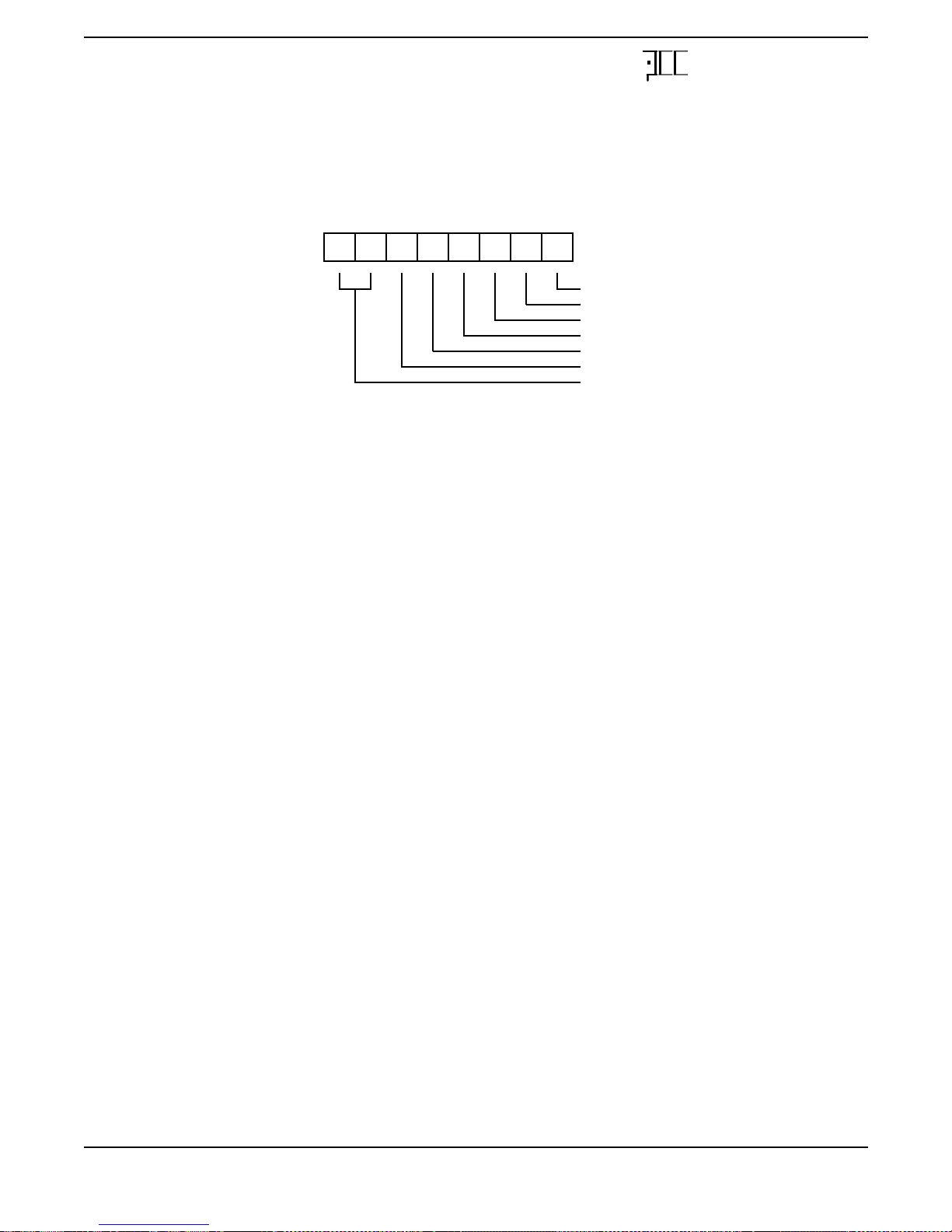
System Status Register 2
Address 60000000h
Byte Read Only
76543210
Reserved
60PE
SCSIPE
DARFPE
EPAKPE
SCSIP
Reserved
Bit Name Function
0 Reserved, mask to zero when read
1 60PE 68060 Parity Error
1 A parity error was detected during a 68060 DRAM read
0 No 68060 Parity error since last read of System Status Register 2
Performance Computer
2 S DMAPE SCSI DMA Parity Error
1 A parity error was detected during a SCSI DMA DRAM read
0 No SCSI DMA Parity error since last read of System Status Register 2
3 SCV64PE SCV64 Parity Error
1 A parity error was detected during a SCV64 DRAM read
0 No SCV64 Parity error since last read of System Status Register 2
4 EPAKPE EPAK Master Parity Error
1 A parity error was detected during a EPAK Master DRAM read
0 No EPAK Parity error since last read of System Status Register 2
5 SCSIP SCSI Present
1 SCSI Controller present
0 SCSI Controller depopulated
7-6 Reserved, mask to zero when read
Extensible Single Board Computer/Controller User’s Manual 65
Page 80
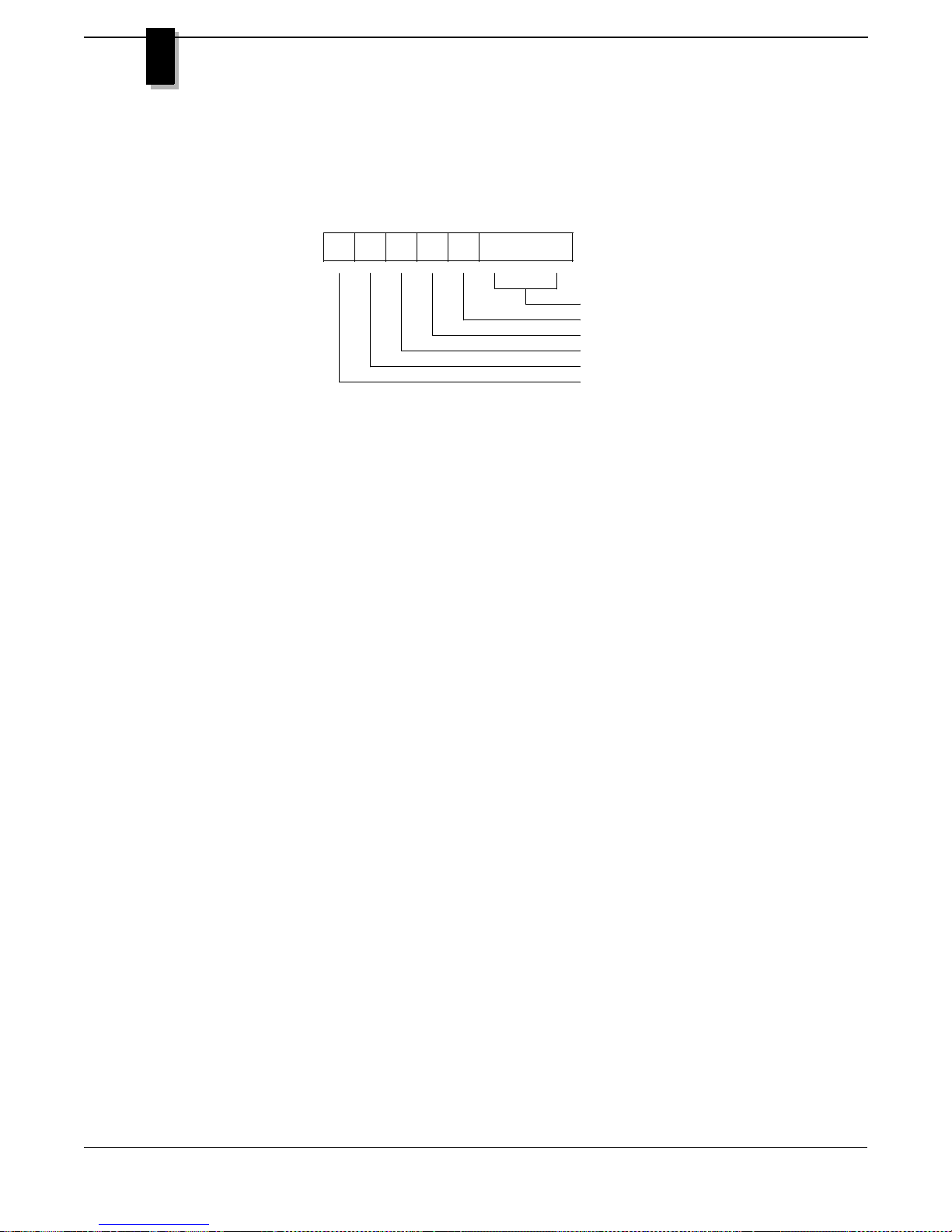
Section
4
FUNCTIONAL SUMMARY
System Status Register 3
Bit Name Function
2-0 DRAMSZ Indicates the amount of DRAM installed
Address 68000000h
Byte Read Only
76543210
DRAMSZ
PARI
ITIP0
ITIP1
ITIP2
Reserved
7-5 Reserved
4 64 Meg
3 32 Meg
2 16 Meg
1 8 Meg
0 4 Meg
3 PARI Parity Installed
1 Parity generation and checking logic installed
0 Parity logic not installed - no parity errors generated
4 ITIP0 Interval Timer 0 Interrupt Pending
1 Interrupt pending
0 No interrupt pending
5 ITIP1 Interval Timer 1 Interrupt Pending
1 Interrupt pending
0 No interrupt pending
6 ITIP2 Interval Timer 2 Interrupt Pending
1 Interrupt pending
0 No interrupt pending
7 Reserved, mask to zero when read
66 Extensible Single Board Computer/Controller User’s Manual
Page 81
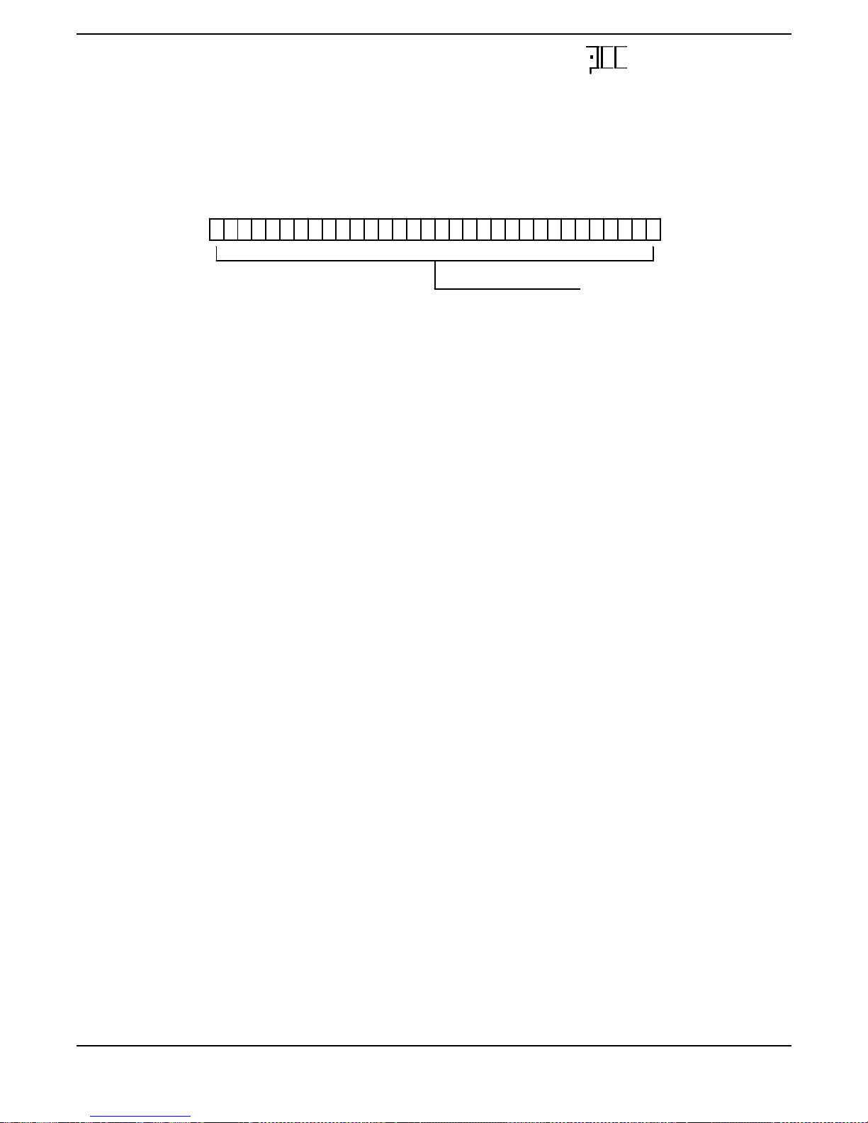
SCSI Memory Address Register
313029282726252423222120191817161514131211109876543210
31-0 SMAR The SCSI Memory Address Register is written with the starting address for a
Jumper List (Defaults)
Performance Computer
Address 0E000000h
Write Only
SMAR[31-0]
SCSI DMA transfer. The register retains its value after reset and is undefined after power u p
This section provides a summary of the jumpers on the PT-VME161 and their default settings.
JUMPER DEFAULT FUNCTION
(Shorted pins)
K1 1 to 2 Reserved
K2 all open MMU Disable (for MC68060 only)
K3 & K11 K3-8 to K3-9 U36 ROM/PROM/SRAM socket configuration
K3-5 to K3-6 64Kx8, 28 pin PROM/ROM device
K3-2 to K3-3
K11 all open
K4 & K10 K4-26 to K4-27 U24 ROM/PROM socket configuration
K4-20 to K4-21 64Kx8, 28 pin PROM/ROM device
K4-16 to K4-17
K4-11 to K4-12
K4-7 to K4-8
K4-5 to K4-6
K4-2 to K4-3
K10 all open
K5 all open Reserved (factory configured)
K6 1 to 2 SCSI Term Power select (1-2 = local, open = SCSI bus)
K7 all open Reserved (factory configured)
K8 1 to 2 4Mb/16Mb DRAM select (1-2 = 4M, factory configured)
K9 1 to 2 4Mb/16Mb DRAM select (2-3 = 16M, factory configured)
Extensible Single Board Computer/Controller User’s Manual 67
Page 82
4
Section
FUNCTIONAL SUMMARY
Interrupt Control
The SCV64 controls local and VMEbus interrupts. Because the SCV64 allows the dynamic assignment
of local interrupts to specific request levels, a fixed interrupt map is unnecessary. The following table
lists the internal and VMEbus interrupt sources and the levels to which they may be assigned. The SCV64
interrupt input pin for each local interrupt request is also shown.
Table 5: Interrupt Request Summary
Interrupt Source Possible Level Assignments SCV64 Input
VMEbus IRQ1 1 (or off) Vectored VIRQ1
VMEbus IRQ2 2 (or off) Vectored VIRQ2
VMEbus IRQ3 3 (or off) Vectored VIRQ3
VMEbus IRQ4 4 (or off) Vectored VIRQ4
VMEbus IRQ5 5 (or off) Vectored VIRQ5
VMEbus IRQ6 6 (or off) Vectored VIRQ6
VMEbus IRQ7 7 (or off) Vectored VIRQ7
Location Monitor 1-7 (or off) Auto-Vectored LIRQ0
VMEbus Events 1-7 (or off) Auto-Vectored LIRQ1
Tick & Interval Timer 1-7 (or off) Auto-Vectored LIRQ2
FAS216 & EPAK [EPIRQ] 1-7 (or off) Auto-Vectored LIRQ3
EPAK [EPVIR] 1-7 (or off) Vectored LIRQ4
68681 1-7 (or off) Vectored LIRQ5
Abort Switch 7 (or off) Auto-Vectored L7I0
Parity Error & SCSI bus Reset 7 (or off) Auto-Vectored L7I1
VMEbus [*ACFAIL] 7 (or off) Auto-Vectored L7I2
VMEbus [*SYSFAIL] 7 (or off) Auto-Vectored L7I3
68 Extensible Single Board Computer/Controller User’s Manual
Page 83
Register Maps
Performance Computer
The “INIT” column in the register map descriptions bel ow identify the initial regi ster values typically
programmed by PTI for our app l ications. All “INIT” values are in hexadecimal, registers that are “don’t
care” at initialization time contain a hyphen.
SCV64
See “APPENDIX H: PT-VME151A Differences From VME131/141” on page 94 for in-depth discussion of initialization issues. See APPENDIX I: and APPENDIX J: for more information.
Table 6: SCV64 Register Map
ADDRESS REGISTER FUNCTION INIT
18000000h DMALAR DMA Local Address Register 18000004h DMAVAR DMA VMEbus Address Register 18000008h DMATC DMA Transfer Count -
1800000Ch DCSR Control and Status Register -
18000010h VMEBAR VMEbus Slave Base Address Register 18000014h RXDATA Receive FIFO Data bits output latch 18000018h RXAD DR Receive FIFO Address bits output
latch
1800001Ch RXCTL Receive FIFO Control bits output latch -
18000020h BUSSEL VMEbus Select 18000024h IVECT VMEbus Interrupt Vector 18000028h APBR Access Protect Boundary -
1800002Ch TXDATA Transmit FIFO Data bits output latch -
18000030h TXADDR Transmit FIFO Address bits output
latch
18000034h TXCTRL Transmit FIFO Control bits output
latch
18000038h LMFIFO Location Monitor FIFO read port -
1800003Ch MODE SCV64 Mode Control -
18000040h SA64BAR Slave A64 Base Address Register 18000044h MA64MAR Master A64 Base Address Register 18000048h LAG Local Address Generator -
1800004Ch DMAVTC DMA VMEbus Transfer Count -
18000050h -
1800007Fh
18000080h STAT0 Status Register 0 18000084h STAT1 Status Register 1 18000088h GENCTL General Control Register 1C
RESERVED
-
-
-
Extensible Single Board Computer/Controller User’s Manual 69
Page 84
Section
4
FUNCTIONAL SUMMARY
ADDRESS REGISTER FUNCTION INIT
1800008Ch VINT VMEbus Interrupter Register -
18000090h VREQ VMEbus Requester Register 03
18000094h VARB VMEbus Arbiter Register 00
18000098h ID ID Register 1800009Ch CTL2 Control & Status Register 2 00
180000A0h 7IS Level 7 Interrupt Status Register 180000A4h LIS Local Interrupt Status Register 180000A8h 7IE Level 7 Interrupt Enable Register -
180000ACh LIE Local Interrupt Enable Register 00
180000B0h VIE VMEbus Interrupt Enable Register 180000B4h IC10 Local Interrupts 1 and 0 Control 13
180000B8h IC32 Local Interrupts 3 and 2 Control 45
180000BCh IC54 Local Interrupts 5 and 4 Control 62
180000C0h MISC Miscellaneous Control Register -
*180000C4h DLCT Delay Line Control Register -
180000C8h DLST1 Delay Line Status Register 1 -
180000CCh DLST2 Delay Line Status Register 2 -
180000D0h DLST3 Delay Line Status Register 3 -
**180000D4h MBOX0 Mailbox register 0 -
**180000D8h MBOX1 Mailbox register 1 -
**180000DCh MBOX2 Mailbox register 2 -
**180000E0h MBOX3 Mailbox register 3 -
180000E4h -
180001FCh
Table 6: SCV64 Register Map
RESERVED
* Initialized by PTBUG. If PTBUG is not us ed, DLCT must be initialized by the u ser with their own
EPROM code or in some other fashion. Also see Appendix F “Mode Register Initialization”, on
page 91.
** Not accessible by the PT-VME161.
70 Extensible Single Board Computer/Controller User’s Manual
Page 85
DS1643 Nonvolatile Timekeeping RAM
Table 7: DS1643 Nonvolatile Timekeeping RAM Registers
ADDRESS FUNCTION VALUES INIT
Performance Computer
0F000000h-
0F001FF7h
0F001FF8h Control Register - 00
0F001FF9h Seconds 00-59 msb = 0
0F001FFAh Minutes 00-59 0F001FFBh Hours 00-23 0F001FFCh Day 01-07 0F001FFDh Date 01-31 0F001FFEh Month 01-12 0F001FFFh Year 00-99 -
Nonvolatile RAM User De finable -
82C54 Interval Timer
Table 8: 82C54 Interval Timer Registers
ADDRESS FUNCTION
70000000h Interval Timer 0 Counter
70000001h Interval Timer 1 Counter
70000002h Interval Timer 2 Counter
70000003h Control Word Register
Extensible Single Board Computer/Controller User’s Manual 71
Page 86
Section
4
FUNCTIONAL SUMMARY
EMULEX FAS216 SCSI Controller
ADDRESS READ FUNCTION WRITE FUNCTION INIT
0A000000h Transfer Counter Low Transfer Count Low 0A000001h Transfer Counter Mid Transfer Count Mid 0A000002h FIFO FIFO 0A000003h Command Command 0A000004h Status Select/Reselect Bus ID 0A000005h Interrupt Select/Reselect Time-out 0A000006h Sequence Step Synchronous Xfer Period 0A000007h FIFO Flags Synchronous Offset 0A000008h Configuration 1 Configuration 1 07
0A000009h Reserved Clock Conversion Factor 05
0A00000Ah Reserved Test mode 0A00000Bh Configuration 2 Configuration 2 20
0A00000Ch Configuration 3 Configuration 3 01
0A00000Dh Reserved Reserved 0A00000Eh Transfer Counter High Transfer Count High 0A00000Fh Reserved Reserve FIFO Byte -
Table 9: EMULEX FAS216 SCSI Controller Register Map
68681 DUART
Table 10: Motorola 68681 DUART Register Map
ADDRESS READ FUNCTION WRITE FUNCTION INIT
08000000h Mode Register A Mode Register A 13-07
08000001h Status Register Clock Select Register A BB
08000002h DO NOT READ Command Register A 08000003h Receiver Buffer A Transmitter Buffer A 08000004h Input Port Change Reg Auxiliary Control Register B0
08000005h Interrupt Status Reg Interrupt Mask Register 33
08000006h Counter Mode: MSB Counter/Timer Upper 08000007h Counter Mode: LSB Counter/Timer Lower 08000008h Mode Register B Mode Register B 13-07
08000009h Status Register B Clock Select Register B BB
0800000Ah DO NOT READ Command Register B 0800000Bh Receiver Buffer B Transmitter Buffer B 0800000Ch Interrupt Vector Reg Interrupt Vector Reg 40
0800000Dh Input Port (unlatched) Output Port Config Reg 00
0800000Eh Start-Counter Command Output Port - Bit Set FF
0800000Fh Stop-Counter Command Output Port - Bit Reset 00
72 Extensible Single Board Computer/Controller User’s Manual
Page 87
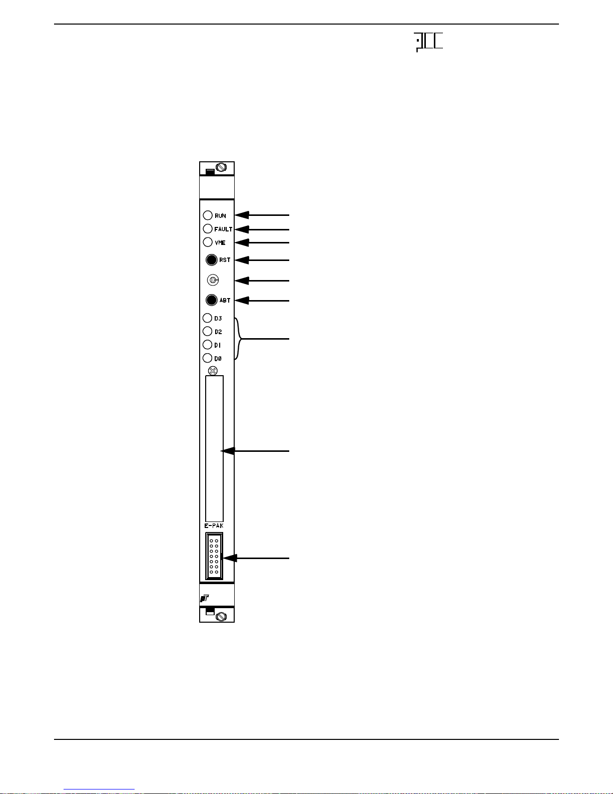
Controls and Indicators
The figure below identifies the controls and indicators that reside on the PT-VME161 Front Panel.
Figure 13: PT-VME161 Front Panel Controls and Indicators
PT-VME
Performance Computer
161
“RUN” Indicator
“FAULT” Indicator
“VME” Indicator
RESET Switch
Rotary Switch
ABORT Switch
VME64
Performance
Technologies
User Programmable LEDs
Optional EPAK I/O Connector
RS-232 Utility Port
Rotary Switch
A hexadecimal rotary switch is provided for utility input purposes. Th e switch st ate is accessible to the
firmware through the System Status Register.
Extensible Single Board Computer/Controller User’s Manual 73
Page 88

Section
4
FUNCTIONAL SUMMARY
“RUN” Indicator
The “RUN” indicator is a green LED which is illuminated whenever the module microprocessor is not
reset and not halted.
“FAULT” Indicator
The “FAULT” indicator is a red LED, under program control, which provides a visual indication to the
user that the software has detected an error condition and the VMEbus signal SYSFAIL* is asserted.
“VME” Indicator
This green indicator is illuminated during the period of a VMEbus master access attempt. The LED illumination intensity is a relative indication of th e PT-VME161’s VMEbus access frequency. A solid,
bright light is indicative of high bus contention where the PT-VME161 is not receiving a Bus Grant.
RESET Switch
The reset switch is a red push button on the front panel which is tied to the EXTRST input pin of the ACC
which in turn generates a board reset [-LRST].
ABORT Switch
The abort switch is a black push button on the front panel which is tied to the -L7I0 (NMI) input pin of
the SCV64 which in turn will generate a level 7 interrupt to the 68060.
User Programmable LEDs
Four user programmable LEDs are available on the front panel, labeled D0, D1, D2, and D3. They are
programmed by software through bits in the System Control Register.
74 Extensible Single Board Computer/Controller User’s Manual
Page 89
Section
5
CONNECTOR PINOUTS
Utility Serial Port Pin Assignments
Connections to the Debug/Utility port can be made using the supplied cable. A Data Terminal Equipment
RS-232C interface is provided. A transition cable is supplied which converts between the 14-pin header
(P3) and a female shell (male pin) 25-pin D-Shell connector.
Table 11: Utility Serial Port Pin Assignments
DB 25 Pin Dir Circuit P3 Pin Description
1 - AA 1 Protective Ground (Shield)
2 Out BA 3 Port A Transmitted Data
3 In BB 5 Port A Received Data
4 Out CA 7 Port A Request To Send
5 In CB 9 Port A Clear To Send
6 In CC 11 Port A Data Set Ready
7 - AB 13 Signal Ground (Common Return)
8-13 Unused
14 Out SBA 2 Port B Tran smitted Data (Secondary)
15 4 Unused
16 In SBB 6 Port B Received Data (Secondary)
17 8 Unused
18 10 Unused
19 12 Unused
20 Out CD 14 Port A Data Terminal Ready
21-25 Unused
Extensible Single Board Computer/Controller User’s Manual 75
Page 90
5
Section
CONNECTOR PINOUTS
VMEbus Pin Assignments
P1A Signal P1B Signal P1C Signal
1 D001BBSY*1D08
2 D012BCLR*2D09
3 D02 3 ACFAIL* 3 D10
4 D034BG0IN*4 D11
5 D04 5 B G0OUT* 5 D12
6 D056BG1IN*6 D13
7 D06 7 B G1OUT* 7 D14
8 D078BG2IN*8 D15
9 GND 9 BG2OUT* 9 GND
10 SYSCLK 10 BG3IN* 10 SYSFAIL*
11 GND 11 BG3OUT* 11 BERR
12 DS1* 12 BR0* 12 SYSRESET*
13 DS0* 13 BR1* 13 LWORD*
14 WRITE* 14 BR2* 14 AM5
15 GND 15 BR3* 15 A23
16 DTACK* 16 AM0 16 A22
17 GND 17 AM1 17 A21
18 AS* 18 AM2 18 A20
19 GND 19 AM3 19 A19
20 IACK* 20 GND 20 A18
21 IACKIN* 21 21 A17
22 IACKOUT* 22 22 A16
23 AM4 23 GND 23 A15
24 A07 24 IRQ7* 24 A14
25 A06 25 IRQ6* 25 A13
26 A05 26 IRQ5* 26 A12
27 A04 27 IRQ4* 27 A11
28 A03 28 IRQ3* 28 A10
29 A02 29 IRQ2* 29 A09
30 A01 30 IRQ1* 30 A08
31 -12V 31 31 +12V
32 +5V 32 +5V 32 +5V
Table 12: VMEbus “P1” Connections
76 Extensible Single Board Computer/Controller User’s Manual
Page 91
Performance Computer
Table 13: VMEbus” P2” Connections
P2A Signal P2B Signal P2C Signal
1 D0 1 +5V 1 GND
2 D1 2 GND 2 GND
3 D2 3 VRMC* 3 GND
4 D3 4 A24 4 GND
5 D4 5 A2 5 GND
6 D5 6 A26 6 GND
7 D6 7 A27 7 GND
8 D7 8 A28 8 GND
9 DP 9 A29 9 GND
10 GND 10 A30 10 GND
11 GND 11 A31 11 GND
12 GND 12 GND 12 GND
13 TPWR 13 +5V 13
14 GND 14 D16 14 GND
15 GND 15 D17 15 GND
16 ATN 16 D18 1 6 GND
17 GND 17 D19 17 GND
18 BSY 18 D20 18 GND
19 ACK 19 D21 19 GND
20 RST 20 D22 20 GND
21 MSG 21 D23 21 GND
22 SEL 22 GND 22 GND
23 C/D 23 D24 23 GND
24 REQ 24 D25 24 GND
25 I/O 25 D26 25 GND
26 26 D27 26 GND
27 27 D28 27 GND
28 28 D29 28 GND
29 29 D30 29 GND
30 30 D31 30 GND
31 31 GND 31 GND
32 32 +5V 32 GND
VMEbus P2 connector rows A and C are User Definable connector pins. The PT-VME161 provides the
connections identified above for the SCSIbus interconnect.
NOTE: VRMC* is a jumper (K7) selectable option. The IEEE 1014 Rev C VMEbus Specification
defines this signal as “RESERVED”.
Pin numbers without mnemonics are not used by the PT-VME161.
Extensible Single Board Computer/Controller User’s Manual 77
Page 92
5
Section
CONNECTOR PINOUTS
EPAK Connectors
The PT-VME161 EPAK module interface is comprised of connectors J1, J2, and J3, and the six EPAK
standoffs.
Table 14: EPAK Connections
J1 Signal J2 Signal J3 Signal
1 +12 1 +MPSZ0 1 +MPA24
2 -12 2 +MPSZ1 2 +MPA25
3 GND 3 +MPFC0 3 +MPA26
4 +MPA00 4 +MPFC1 4 +MPA27
5 +MPA01 5 +MPFC2 5 +MPA28
6 +MPA02 6 GND 6 +MPA29
7 +MPA03 7 +MPA08 7 +MPA30
8 +MPA04 8 +MPA09 8 +MPA31
9 +MPA05 9 +MPA10 9 GND
10 +MPA06 10 +MPA11 10 +MPD00
11 +MPA07 11 +MPA12 11 +MPD01
12 GND 12 +MPA13 12 +MPD02
13 +MPD24 13 +MPA14 13 +MPD03
14 +MPD25 14 +MPA15 14 +MPD04
15 +MPD26 15 GND 15 +MPD05
16 +MPD27 16 +MPA16 16 +MPD06
17 +MPD28 17 +MPA17 17 +MPD07
18 +MPD29 18 +MPA18 18 GND
19 +MPD30 19 +MPA19 19 +MPD08
20 +MPD31 20 +MPA20 20 +MPD09
21 GND 21 +MPA21 21 +MPD10
22 -EPSEL 22 +MPA22 22 +MPD11
23 -MPRMC 23 +MPA23 23 +MPD12
24 -MPUAS 24 GND 24 +MPD13
25 -MPUDS 25 +MPD16 25 +MPD14
26 -MPWRT 26 +MPD17 26 +MPD15
27 -EPSA0 27 +MPD18 27 GND
28 -EPIRQ 28 +MPD19 28 -MPSA0
29 -EPVIR 29 +MPD20 29 -MPSA1
30 -EPVIA 30 +MPD21 30 -MPBER
31 +EPKIO 31 +MPD22 31 -MPHLT
32 GND 32 +MPD23 32 -EPKPE
33 +MPCLK 33 GND 33 GND
34 -MPCLK 34 -EPSA1 34 -EPKBR
35 -MPRST 35 -EPERR 35 -MPBGA
36 -BDRST 36 +REFCK 36 -EPKBG
78 Extensible Single Board Computer/Controller User’s Manual
Page 93
DRAM Module
Performance Computer
The EPAK mounting standoffs are used to carry power and ground to the EPAK module.
Table 15: EPAK mounting standoffs
Mounting pin Signal
1GND
2+5V
3GND
4+5V
5GND
6GND
The DRAM Module standoff carries ground to the module.]
Table 16: DRAM Module Connections
Pin Signal Pin Signal
1 GND 41 GND
2D042D8
3D143D9
4D244D10
5D345D11
6D446D12
7D547D13
8D648D14
9D749D15
10 GND 50 GND
11WE051WE1
12 GND 52 GND
13 RAS0 53 RAS1
14 A0 54 A6
15 A1 55 A7
16 A2 56 A8
17 MSIZ2 57 GND
18 MSIZ0 58 CAS1
19 GND 59 GND
20 MSIZ1 60 PERR
21 GND 61 SPARE
22 CAS0 62 PARPR
Extensible Single Board Computer/Controller User’s Manual 79
Page 94
Section
5
CONNECTOR PINOUTS
Table 16: DRAM Module Connections
Pin Signal Pin Signal
23 GND 63 OE
24 A3 64 A9
25 A4 65 A10
26 A5 66 A11
27 GND 67 GND
28 RAS2 68 RAS3
29 PTST 69 RASP
30WE270WE3
31 GND 71 GND
32D1672D24
33D1773D25
34D1874D26
35D1975D27
36D2076D28
37D2177D29
38D2278D30
39D2379D31
40 GND 80 GND
The DRAM mounting standoffs are used to carry power and ground to the DRAM module.
Table 17: EPAK mounting standoffs
Mounting pin Signal
1+5V
2+5V
3GND
80 Extensible Single Board Computer/Controller User’s Manual
Page 95
Section
6
MECHANICAL AND
ENVIRONMENTAL
Power Requirements
The following values are without an EPAK installed.
Ambient Temperature
Table 18: Power Requirements
Voltage Typical Maximum
+5V (±5%) 3.9 Amps 4.4 Amps
+12V (±5%) 25 mA 42 mA
-12V (±5%) 25 mA 42 mA
Humidity
Vibration
Table 19: Ambient Temperature
Use Minimum Maximum
Operating 0° C +55° C
Storage -55° C +85° C
Non condensing
Table 20: Humidity Constraints
Minimum Maximum
0% 90%
Designed to meet 5-100 Hz with 2g Acceleration.
Extensible Single Board Computer/Controller User’s Manual 81
Page 96
6
Section
MECHANICAL AND ENVIRONMENTAL
Mechanical Shock
Designed to meet 20g for 6 ms (half sine).
Physical Dimensions
Base board only
Table 21: Physical Dimensions
Dimension Millimeters Inches
Width 234 9.2
Depth 160 6.3
Front Panel 20.3 .80
Component Height 14 .55
82 Extensible Single Board Computer/Controller User’s Manual
Page 97

Section
7
APPENDICES
APPENDIX A: Product Warranty
Performance Computer, A Performance Technologies Company (hereinafter “PCC”)
warrants that its products sold hereunder will at the time of shipment be free from
defects in material and workmanship and will conform to PCC’s applicable specifications or, if appropriate, to Buyer’s specifications accepted by PCC in writing. If products sold hereunder are not as warranted, PCC shall, at its option, refund the purchase
price, repair, or replace the product provided proof of purchase and written notice of
nonconformance are received by PCC within 12 months of shipment, or in the case of
software and integrated circuits within ninety (90) days of shipment and provided said
nonconforming products are returned F.O.B. to PCC’s facility no later than thirty days
after the warranty period expires. Products returned under warranty claims must be
accompanied by an approved Return Material Authorization number issued by PCC
and a statement of the reason for the return. Please contact PCC, or its agent, with the
product serial number to obtain an RMA number. If PCC determines that the products
are not defective, Buyer shall pay PCC all costs of handling and transportation. This
warranty shall not apply to any products PCC determines to have been subject to testing
for other than specified electrical characteristics or to operating and/or environmental
conditions in excess of the m aximum values es tablished in a pplicable specifications, or
have been subject to mishandling, misuse, static discharge, neglect, improper testing,
repair, alteration, parts removal, damage, assembly or processing that alters the physical or electrical properties. This warranty excludes all cost of shipping, customs clearance and related charges outside the United States. Products containing batterie s are
warranted as above excluding batteries.
THIS WARRANTY IS IN LIEU OF ALL OTHER WARRANTIES WHETHER
EXPRESS, IMPLIED OR STATUTORY INCLUDING IMPLIED WARRANTIES
OF MERCHANTABILITY OR FITNESS. IN NO EVENT SHALL PCC BE LIABLE
FOR ANY INCIDENTAL OR CONSEQUENTIAL DAMAGES DUE TO BREACH
OF THIS WARRANTY OR ANY OTHER OBLIGATION UNDER THIS ORDER
OR CONTRACT.
Extensible Single Board Computer/Controller User’s Manual 83
Page 98

7
Section
APPENDICES
APPENDIX B: Product Return Procedure
If you find that your Performance Computer (“PCC”) product must be returned for repair, note the
following:
To return equipment, please obtain a Return Material Authorization (RMA) number. PCC cannot accept
returns without an RMA number.
To obtain an RMA numb er, contact PCC’ s Customer S ervice Group at (716) 256-0 248 (FAX: (716) 256-
0791). Outside North America, Customers should contact their PCC agent. PCC requests the serial
number of the unit and the reason for the return at the time the RMA is issued.
Return products should be shipped, prepaid, to:
Performance Technologies, Incorporated
Attn: Customer Service Group
315 Science Parkway
Rochester, N.Y. 14620, U.S.A.
(Customers outside of North America, contact your local PCC agent for return shipment instructions.)
The RMA number should be marked on the outside of the shipping box to expedite correct handling at
the PCC factory.
Repairs will be performed only on complete units. Return of incomplete equipment may delay repairs.
Please note that removal of original parts or product modification by a customer can void the warranty.
(This does not apply to jumpers or socketed user programmable parts.)
“Out of warranty repairs” cannot proceed without a customer Purchase Order.
PCC will supply repair information on all ret urn s.
PCC warrants all repairs for 90 days.
84 Extensible Single Board Computer/Controller User’s Manual
Page 99

APPENDIX C: Product Support
IF YOU ENCOUNTER DIFFICULTY IN USING THIS PERFORMANCE COMPUTER SBus
!
PRODUCT, YOU CAN CONTACT OUR SUPPORT PERSONNEL IN ONE OF THREE WAYS.
A) Preferred - If you have Internet services - email us at [email protected]. Outline your problem
in detail. Please include your return email address, and a telephone number.
B) FAX - If you have FAX service, contact our FAX Number at (716) 256-0791. Mark your FAX
to Attention: VME Product Support. Outline your problem in detail. Please include your return FAX
number and a telephone number.
C) Contact us via telepho ne at U. S. Area Co de 716- 256-02 48. P roduct S upport i s avail able between
8:00 am and 5:00 pm Eastern Time, Monday through Friday.
In addition, Performance Computer supports an inter net mail server. This can b e used to get up dated
drivers and other information on PCC’s products, You can request a usage document by sending
electronic mail to the server, with nothing in the body of the email text (no signature files). The
server’s internet address is:
Performance Computer
If you are located outside North America, we encourage you to contact the local PCC distributor or
agent for support. Many of our distributors or agents maintain technical support staffs.
Extensible Single Board Computer/Controller User’s Manual 85
Page 100

7
Section
APPENDICES
APPENDIX D: Installation Notes
CAUTION: ELECTRONIC COMPONENTS ON PRINTED CIRCUIT BOARDS ARE EXTREMELY
!
!
!
SENSITIVE TO STATIC ELECTRICITY. ORDINARY AMOUNTS OF STATIC ELECTRICITY
GENERATED BY YOUR CLOTHING OR WORK ENVIRONMENT CAN DAMAGE THE ELECTRONIC EQUIPMENT. IT IS RECOMMENDED THAT WHEN INSTALLING THE PT-VME161 IN
A SYSTEM OR THE COMPONENTS ON THE BOARD ITSELF THAT ANTI-STATIC
GROUNDING STRAPS AND ANTI-STATIC MATS ARE USED TO HELP PREVENT DAMAGE
DUE TO ELECTROSTATIC DISCHARGE.
CAUTION: WHEN INSTALLING CHIPS INTO PROM SOCKETS, BE CERTAIN OF THEIR
ORIENTATIONS. THE BOTTOM OF THE CHIP WILL BE ALIGNED WITH THE BOTTOM OF
THE SOCKET. THE TOP OF THE SOCKET IS THE END CLOSEST TO THE VME CONNECTORS.
PIN ONE OF THE CHIP SHOULD BE POINTING TOWARD THE VME CONNECTORS.
CAUTION: WHEN INSTALLING A 28 PIN DEVICE BE SURE THAT PIN 14 OF THE DEVICE
ENTERS PIN 16 OF THE SOCKET (BOTTOM JUSTIFIED).
86 Extensible Single Board Computer/Controller User’s Manual
 Loading...