

Page 1
Page 2

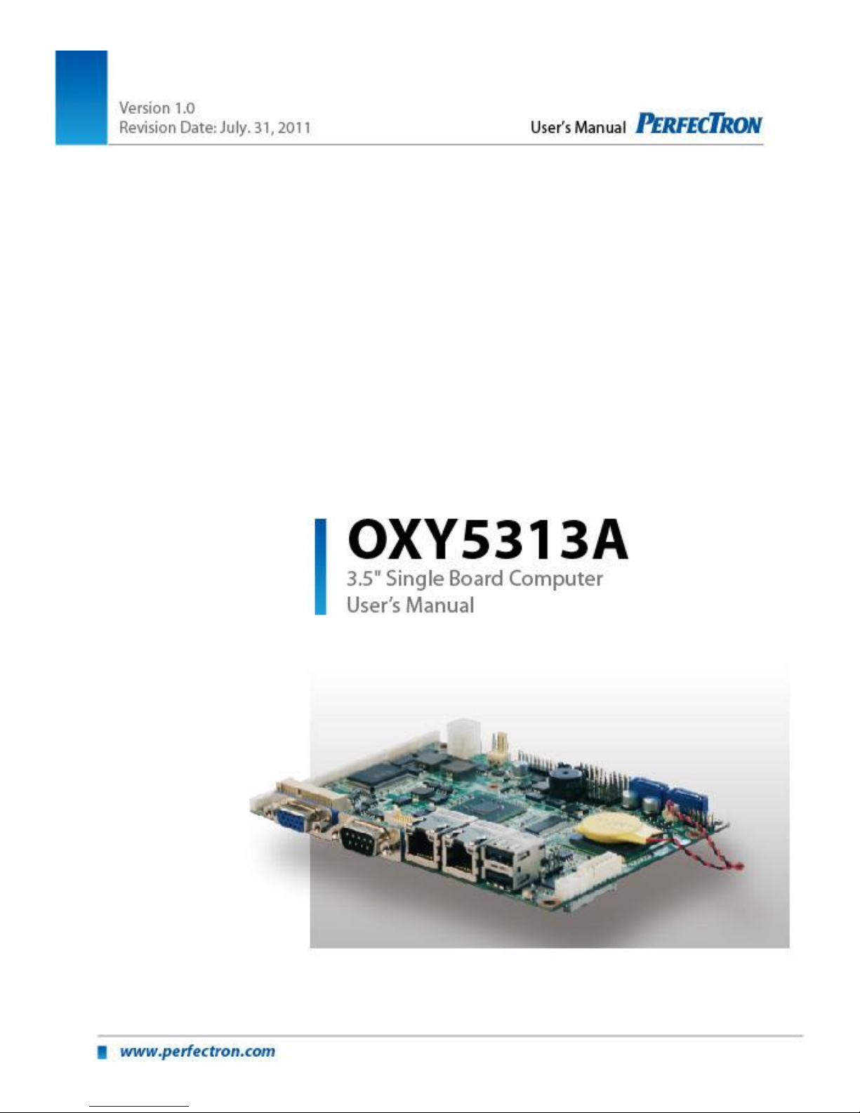
OXY5313A 3.5” SBC User’s Manual
ii
Safety information
Electrical safety
To prevent electrical shock hazard, disconnect the power cable from the electrical
outlet before relocating the system.
When adding or removing devices to or from the system, ensure that the power
cables for the devices are unplugged before the signal cables are connected. If
possible, disconnect all power cables from the existing system before you add a
device.
Before connecting or removing signal cables from the motherboard, ensure that all
power cables are unplugged.
Seek professional assistance before using an adapter or extension cord. These
devices could interrupt the grounding circuit.
Make sure that your power supply is set to the correct voltage in your area.
If you are not sure about the voltage of the electrical outlet you are using, contact
your local power company.
If the power supply is broken, do not try to fix it by yourself. Contact a qualified
service technician or your local distributor.
Operation safety
Before installing the motherboard and adding devices on it, carefully read all the
manuals that came with the package.
Before using the product, make sure all cables are correctly connected and the
power cables are not damaged. If you detect any damage, contact your dealer
immediately.
To avoid short circuits, keep paper clips, screws, and staples away from connectors,
slots, sockets and circuitry.
Avoid dust, humidity, and temperature extremes. Do not place the product in any
area where it may become wet.
Place the product on a stable surface.
If you encounter any technical problems with the product, contact your local
distributor
Statement
All rights reserved. No part of this publication may be reproduced in any form or by
any means, without prior written permission from the publisher.
All trademarks are the properties of the respective owners.
All product specifications are subject to change without prior notice
Page 3
OXY5313A 3.5” SBC User’s Manual
iii
Revision History
Revision
Date (dd.mm.yyyy)
Changes
Version 1.0
31.07.2011
Initial release
Version 1.1
05.09.2011
Updated Packing list for Cab le
kit
Modified 3P Clear CMOS to 2P
Removed JUSB_01
Removed JCOMPWR1-6
Packing list
□ OXY5313A 3.5” SBC
□ Driver CD
□ Quick Installation Guide
□ User’s Manual
□ Fanless Thermal Module(Optional)
□ Cable kit with as below cable(Optional)
Item list
Product description
Quantity
Ordering P/N
Audio Cable
L-IN+MIC+L-
OUT ψ3.5 Phone JACK 180D
to XH-6 1x6P P:2.54mm 180D, L:150mm
Lead Free
1 0C50200AUDIO000
L
SATA Cable
7P + JACKET W/LOCK Female
帶鐵彈片
P:1.27mm 180D L:200mm Lead Free
1 0C50200SATA0000L
LPT Cable DB25 D-SUB w/bracket(附 2PCS 六角螺
絲) Female 25P 180D to IDC 2*13P
P:2.00mm, L:205mm 180D LEAD FREE
1 0C5030010008010L
KB/MS Cable KB+MS MD-6S Female 6P to 6008H
2x3pin P:2.54mm 杜
邦 Female 180D,
L:170mm LEAD FREE
1 0C50200KBMSPS20
L
COM Cable Male 180D to 51021-1000(Molex1.25-
10P)1x10P,P:1.25mm ,180D, L:300mm
TUBE:200mm LEAD FREE
1 0C5020010008010L
If any of the above items is damaged or missing, please contact your local
distributor.
Page 4

OXY5313A 3.5” SBC User’s Manual
iv
Table of Contents
Safety information ................................................................................................................................................ i
Electrical safety .......................................................................................................................................... ii
Operation safety ........................................................................................................................................ ii
Statement ................................................................................................................................................... ii
Revision History ........................................................................................................................................ iii
Packing list ................................................................................................................................................ iii
Chapter 1: Product Information ................................................................................................................ 7
1.1 Block Diagram .................................................................................................................................... 7
1.2 Key Features ...................................................................................................................................... 8
1.3 Board Placement ................................................................................................................................ 9
1.4 Onboard Connector List ................................................................................................................... 10
1.5 Mechanical Drawings ....................................................................................................................... 11
2.1 Jumper Settings ............................................................................................................................. 12
JCMOS1: Clear CMOS Jumper Setting ......................................................................................... 12
PSON1: ATX/AT mode Selection ................................................................................................... 12
2.2 Onboard Connector Pin Assignment........................................................................................... 13
MPCIE1 Mini PCIE slots V1.2 ....................................................................................................... 13
ATX1 DC Power Input Connector .................................................................................................. 14
Digital I/O Pin Header ..................................................................................................................... 14
COM2~4 RS-232 Port (1x10 pin Wafer) ........................................................................................ 14
COM5~8 RS-232 Port Wafer......................................................................................................... 15
LPT1 Parallel Port Pin Header ....................................................................................................... 15
SPD/IF output pin Header .............................................................................................................. 15
AUDIO1 Audio Output Wafer ......................................................................................................... 16
AMP_R1 Audio AMP Right Output Wafer...................................................................................... 16
AMP_L1 Audio AMP Left Output Wafer ........................................................................................ 16
DDR3_1 DDR3 Memory DIMM Slot ............................................................................................... 16
CPU/System FAN ........................................................................................................................... 16
FD1 CF Type II Connector ............................................................................................................ 17
FP1 Front Panel 1 Pin Header .............................................................................................................. 17
FP2 Front Panel 2 Pin Header .............................................................................................................. 18
SATAI1, SATA2 Serial ATA 2.0 Connector........................................................................................... 18
USB2,USB3,USB4 USB2.0 Pin Header ........................................................................................ 18
JTAG1 TAG Port Box Header ........................................................................................................ 18
JLVDS1 18 bit LVDS Panel Connector......................................................................................... 19
KBMS1 KB/MS Pin Header ........................................................................................................... 19
JBKL1 Panel Backlight Wafer ....................................................................................................... 19
COM1 (RS-232/422/485 Port A DB-9 Connector) .......................................................................... 19
LAN1 , LAN2 10/100/1000 Ethernet RJ-45 Connector ................................................................ 20
VGA1 CRT DB-15 Connector ........................................................................................................ 20
USB1 2-Stack USB2.0 Type A Connector ..................................................................................... 20
Chapter 3: Getting Started ............................................................................................................................... 21
3.1 Installing System Memory ................................................................................................................ 21
3.2 installing the CF card ........................................................................................................................ 21
3.3 Driver Installation .............................................................................................................................. 22
Chapter 4: AMI BIOS UTILITY ............................................................................................................... 23
4.1 Starting .............................................................................................................................................. 23
4.2 Navigation Keys ................................................................................................................................ 23
4.3 Main Menu ........................................................................................................................................ 24
SATA 1 Setup ......................................................................................................................................... 25
Page 5

OXY5313A 3.5” SBC User’s Manual
v
SATA 1(LBA/Large Mode) ...................................................................................................................... 25
SATA 1(DMA Mode) ............................................................................................................................... 26
SATA 2 Setup ......................................................................................................................................... 27
SATA 2(LBA/Large Mode) ...................................................................................................................... 27
SATA 2(LBA/Large Mode) ...................................................................................................................... 28
S.M.A.R.T for SATA 2............................................................................................................................. 28
CF Setup ................................................................................................................................................. 29
CF setup(LBA/Large Mode) .................................................................................................................... 29
CF (DMA Mode) ...................................................................................................................................... 30
S.M.A.R.T for CF .................................................................................................................................... 31
System Information ................................................................................................................................. 32
4.4 Advanced Menu ................................................................................................................................ 33
Onboard I/O Configuration ..................................................................................................................... 33
Onboard Peripherals Configuration ........................................................................................................ 35
USB Function .......................................................................................................................................... 35
USB Device Legacy Support .................................................................................................................. 36
Audio Controller ...................................................................................................................................... 36
Onboard LAN1 Controller ....................................................................................................................... 37
Onboard LAN1 OPTROM ....................................................................................................................... 37
Onboard LAN2 Controller ....................................................................................................................... 38
Onboard LAN2 OPTROM ....................................................................................................................... 38
Onboard Mini-PCIE Controller ................................................................................................................ 39
On-Chip ATA Devices............................................................................................................................. 40
ATA/IDE Configuration ........................................................................................................................... 40
Configure SATA as ................................................................................................................................. 41
Hardware Health Configuration .............................................................................................................. 42
4.5 Boot Setting ...................................................................................................................................... 43
Quick Boot .............................................................................................................................................. 43
Full Screen Logo Display ........................................................................................................................ 43
Bootup Num-lock .................................................................................................................................... 44
Wait For ‘F1’ If Error ............................................................................................................................... 44
Hit ‘Del’ Message Display ....................................................................................................................... 45
4.6 Chipset Setting ................................................................................................................................. 45
Initial Graphic Adapter ............................................................................................................................ 46
Internal Graphic Mode Select ................................................................................................................. 46
Hyper Threading Technology ................................................................................................................. 47
Video Function Configuration ................................................................................................................. 48
DVMT Model Select ................................................................................................................................ 48
DVMT/Fixed Memory .............................................................................................................................. 49
Boot Display Device................................................................................................................................ 49
Flat Panel Type ....................................................................................................................................... 50
Panel Backlight voltage .......................................................................................................................... 50
4.7 Power Management Setting ............................................................................................................. 51
ACPI Function ......................................................................................................................................... 51
ACPI Standby State ................................................................................................................................ 52
Repost Video on S3 Resume ................................................................................................................. 52
Restore on AC Power Loss .................................................................................................................... 53
Resume From S3 By USB Device .......................................................................................................... 54
Resume By LAN Device ......................................................................................................................... 54
Resume By RTC Alarm .......................................................................................................................... 55
4.8 Security Setting................................................................................................................................. 55
Change Supervisor Password ................................................................................................................ 56
Change User Password .......................................................................................................................... 56
Page 6

OXY5313A 3.5” SBC User’s Manual
vi
4.9 Exit Setting ........................................................................................................................................ 57
Save Changes and Exit .......................................................................................................................... 57
Discard Changes and Exit ...................................................................................................................... 59
Discard Changes .................................................................................................................................... 60
Load Optimal Defaults ............................................................................................................................ 61
Load Failsafe Defaults ............................................................................................................................ 62
APPENDIX A Watchdog Timer Setting ............................................................................................................ 63
APPENDIX B DIGITAL I/O ............................................................................................................................... 65
Page 7
OXY5313A 3.5” SBC User’s Manual
7
Chapter 1: Product Information
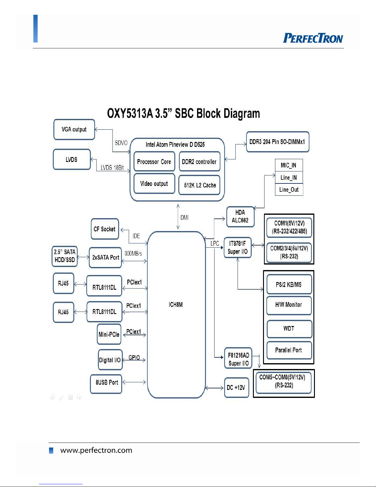
1.1 Block Diagram
Page 8
OXY5313A 3.5” SBC User’s Manual
8
1.2 Key Features
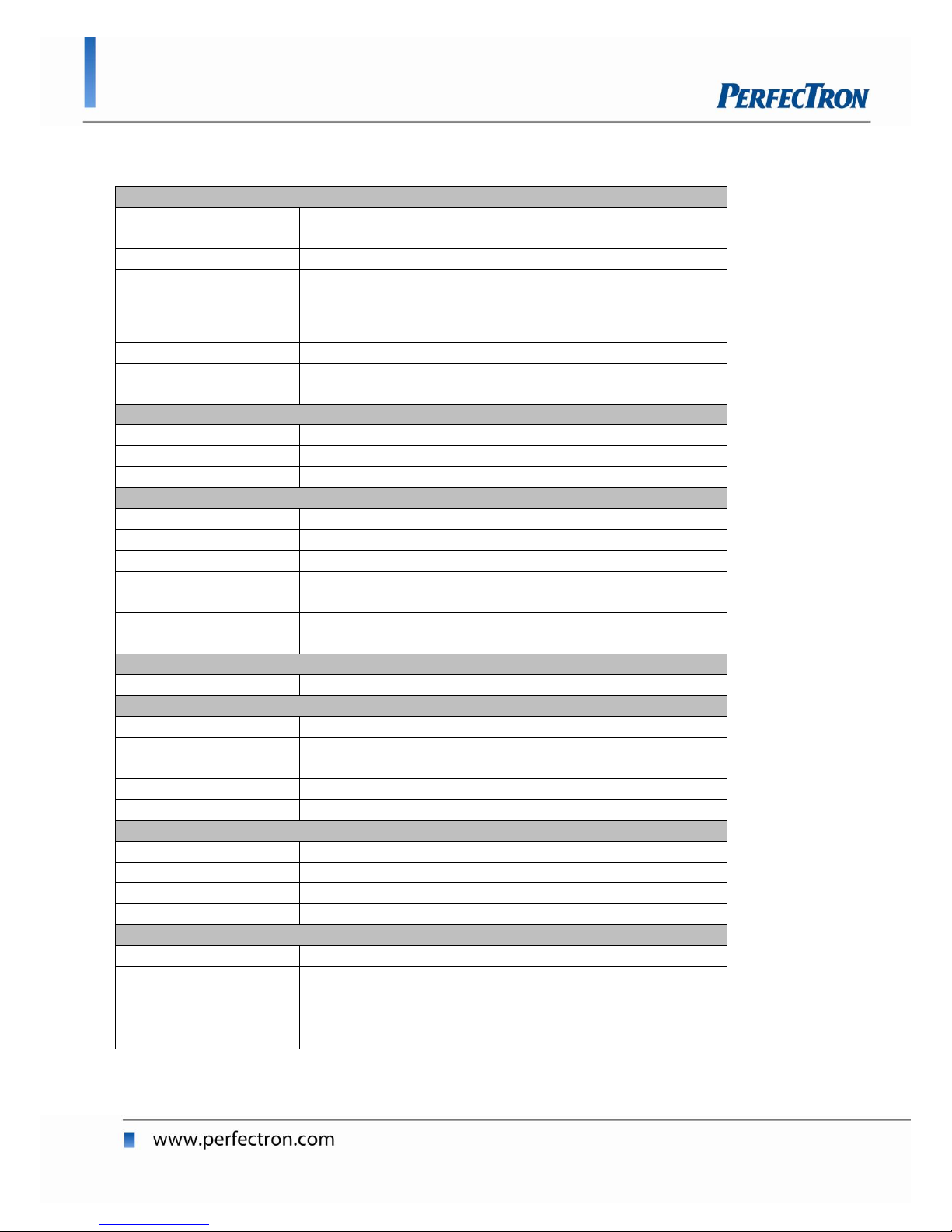
Processor & System
CPU Type
Intel Atom Pineview D D525 CPU onboard
(45nm,1.8Ghz , 1M L2 Cache)
Chipset
Intel® ICH8M
Memory Type
DDR3 800 SO-DIMM(Max is 2GB)
BIOS
8MB SPI Flash
Super I/O
ITE8781F
Watchdog
1-255 sec. or 1-255 min. software programmable
and can be generate system reset
Expansion Slot
CF Socket
CF Type I/II CF Socket
SATA Port
2 x SATAII (3Gb/s)
Mini-PCIe Socket
Supports GPRS/GSM Mini-PCIe Devices
Display
Chipset
Integrated Intel® GMA3150 Graphic engine
Memory Size
Intel® DVMT 4.0 compliant
Onboard VGA
Yes, Max.: SXGA 2048 x 1536
LVDS
18-bit single channel LVDS
24-bit single/dual channel LVDS (By LVDS card)
Dual Displays
Capability
VGA+LVDS
Audio
Codec
ALC662 High Definition Audio Codec
Ethernet
Controller
Dual Realtek RTL8111DL PCIex1 Bus
Disable LAN through
BIOS
Yes
WOL
Yes
Boot from LAN
Yes for PXE
Rear I/O
VGA
1 Port
Ethernet
2 Port
COM
1 x RS232/422/485 with 5V/12V selectable (COM1)
USB 1.1/2.0
4 Port
Internal I/O
SATA
2 x SATAII (3Gb/s)
USB
Total is 8xUSB Port
*2 Port on Front I/O
*6 Port by 2x5 pin header
COM
Total is 8xCOM port
Page 9
OXY5313A 3.5” SBC User’s Manual
9
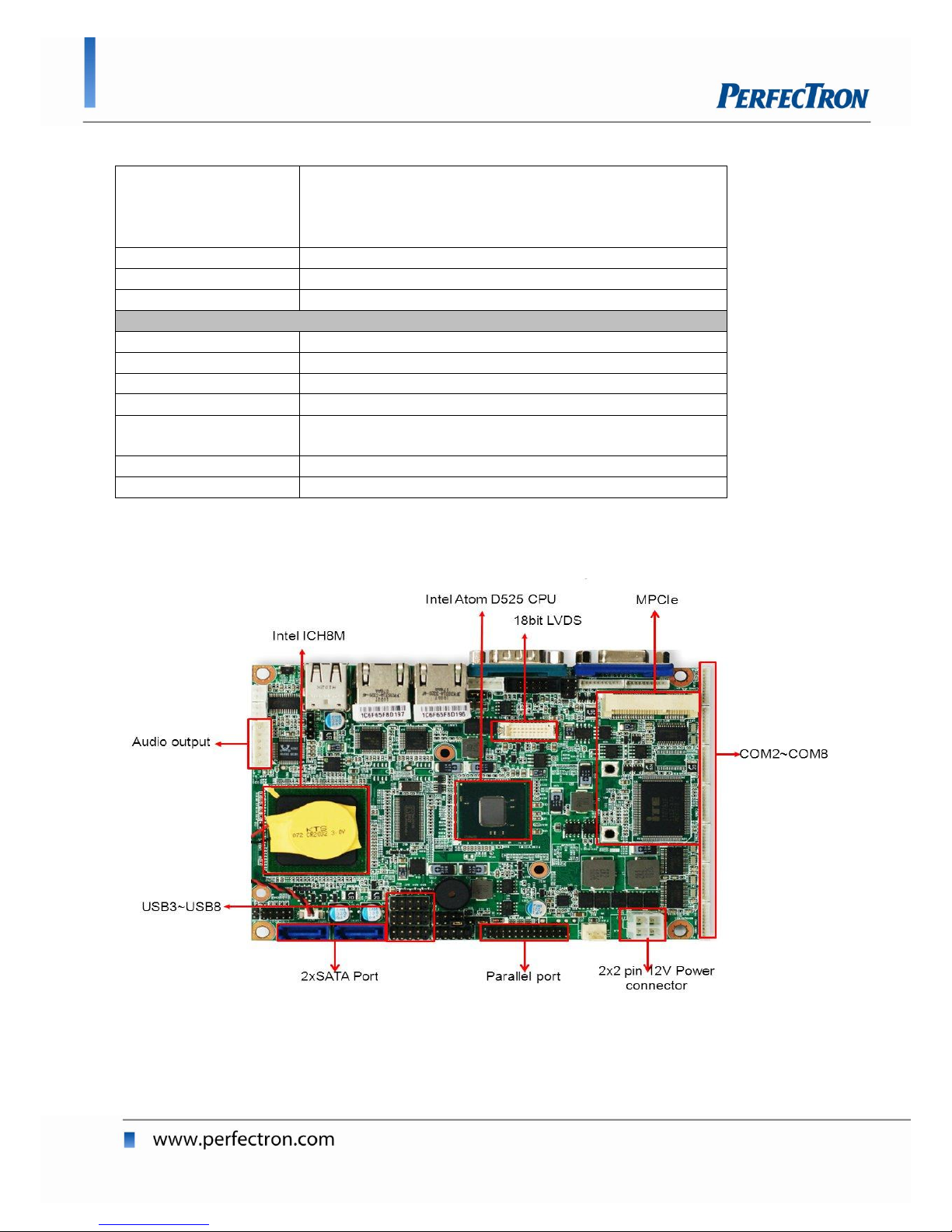
COM1 belongs to D-Sub 9pin and supports RS232/422/485)
COM2~COM8 belongs to 10pin Wafer connector
and supports RS232 only
SPDIF
1x5 Pin header
Digital I/O
2x5 Pin header (4in and 4 out)
Parallel port
2x13 Pin Box header
Mechanical and Environment
Form Factor
3.5” SBC
Power Type
ATX 2x2 pin Power connector
Voltage
+12V single voltage in
Dimension
146 mm x 102mm
Operating
Temperature
-20°C-70°C
Storage Temperature
-20°C-80°C
Relative humidity
10% to 90%, non-condensing
* All specifications and photos are subject to change without notice*
1.3 Board Placement
Page 10
OXY5313A 3.5” SBC User’s Manual
10
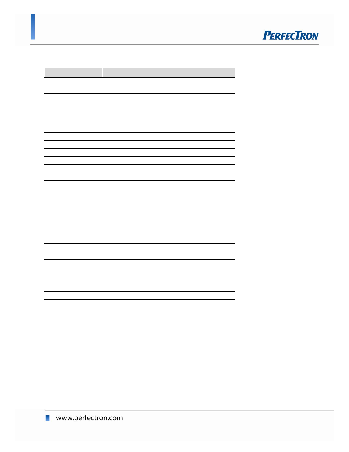
1.4 Onboard Connector List
Label
Function
MPCIE1
Mini PCIe Connector
ATX2
Power Input Connector
DIO1
Digital Input / Output Pin Header
COM2
RS-232 Port B With Power Wafer
COM3
RS-232 Port C With Power Wafer
COM4
RS-232 Port D With Power Wafer
COM5
RS-232 Port E With Power Wafer
COM6
RS-232 Port F With Power Wafer
COM7
RS-232 Port G With Power Wafer
COM8
RS-232 Port H With Power Wafer
LPT1
Parallel Port Pin Header
SPDIF1
SPD/IF Output Pin Header
AUDIO1
AUDIO OUT Wafer
AMP_R1
Audio AMP Right Output Wafer
AMP_L1
Audio AMP Left Output Wafer
DDR3_1
DDR3 Memory SO-DIMM Socket
FAN1
CPU FAN Wafer
CFD1
CF Type II Connector
FP1
Front Panel 1 Pin Header
FP2
Front Panel 2 Pin Header
SATA1
Serial ATA 2.0 Connector
SATA2
Serial ATA 2.0 Connector
USB2
USB2.0 Port 3, 4 Pin Header
USB3
USB2.0 Port 5, 6 Pin Header
USB4
USB2.0 Port 7, 8 Pin Header
JTAG1
Intel JTAG Box Header
JLVDS1
LVDS Panel Connector
KBMS1
KB/MS Pin Header
JBKL1
Panel Backlight Wafer
Page 11
OXY5313A 3.5” SBC User’s Manual
11
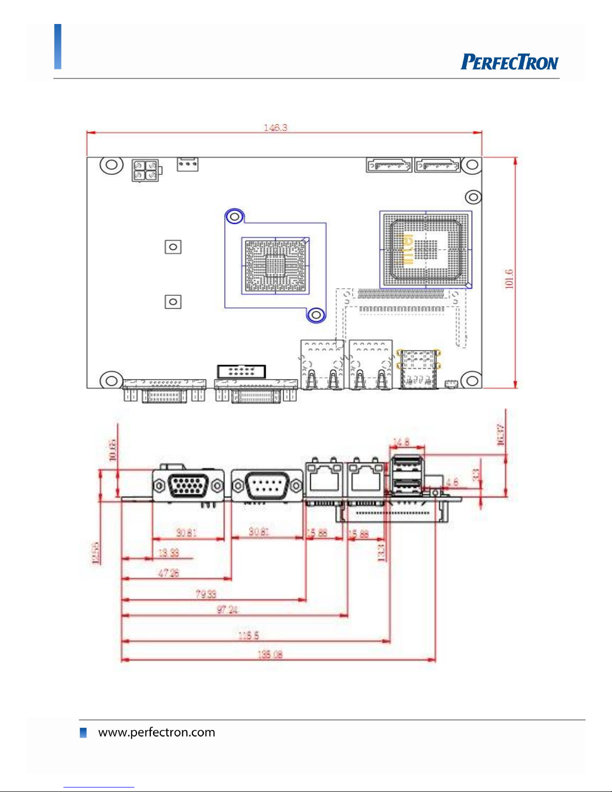
1.5 Mechanical Drawings
Page 12
OXY5313A 3.5” SBC User’s Manual
12
Chapter 2: Jumpers and Connectors
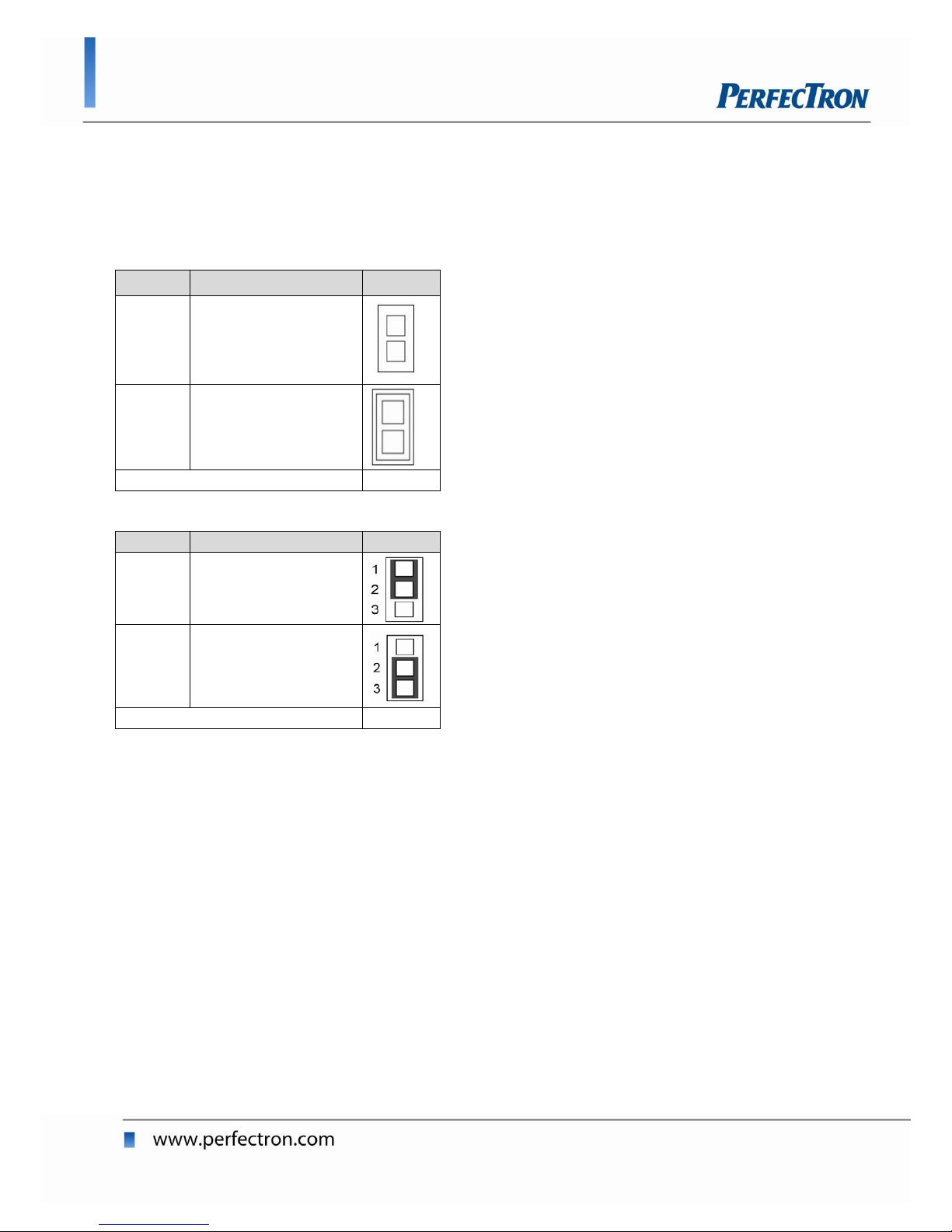
2.1 Jumper Settings
JCMOS1: Clear CMOS Jumper Setting
Jumper
Function description
Setting
1-2
Normal Operation
2-3
Clear CMOS
*Default setting is 1-2*
PSON1: ATX/AT mode Selection
Jumper
Function description
Setting
1-2
AT Mode
2-3
ATX Mode
*Default setting is 2-3*
Page 13
OXY5313A 3.5” SBC User’s Manual
13
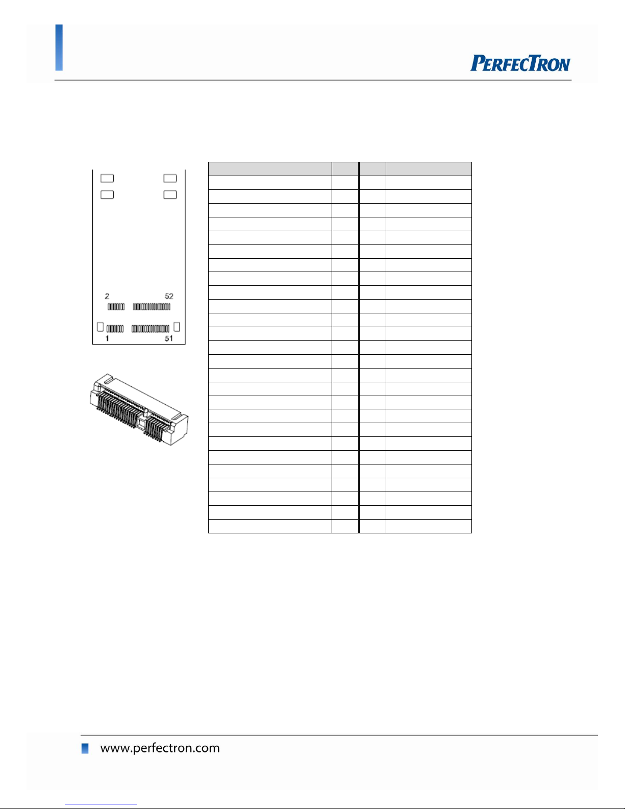
2.2 Onboard Connector Pin Assignment
MPCIE1 Mini PCIE slots V1.2
Signal Name
Pin
Pin
Signal Name
PCIE_WAKE#
1 2 *+3.3VSB
NC 3 4
GND
NC 5 6
+1.5V
NC 7 8
UIM_PWR
GND
9
10
UIM_DATA
CLK100_MPCIE1#/2#
11
12
UIM_CLK
CLK100_MPCIE1/2
13
14
UIM_RESET
GND
15
16
UIM_VPP
NC
17
18
GND
NC
19
20
MPCIE1/2_EN
GND
21
22
RST_PCIE#
PCIE_RX2-/3-
23
24
+3.3VSB
PCIE_RX2+/3+
25
26
GND
GND
27
28
+1.5V
GND
29
30
SB_SMB_CLK
PCIE_TX2-/3-
31
32
SB_SMB_DAT
PCIE_TX2+/3+
33
34
GND
GND
35
36
USBN
GND
37
38
USBP
+3.3VSB
39
40
GND
+3.3VSB
41
42
LED_WLAN#
GND
43
44
LED_WLAN#
NC
45
46
LED_WLAN#
NC
47
48
+1.5v
NC
49
50
GND
NC
51
52
*+3.3VSB
Page 14
OXY5313A 3.5” SBC User’s Manual
14
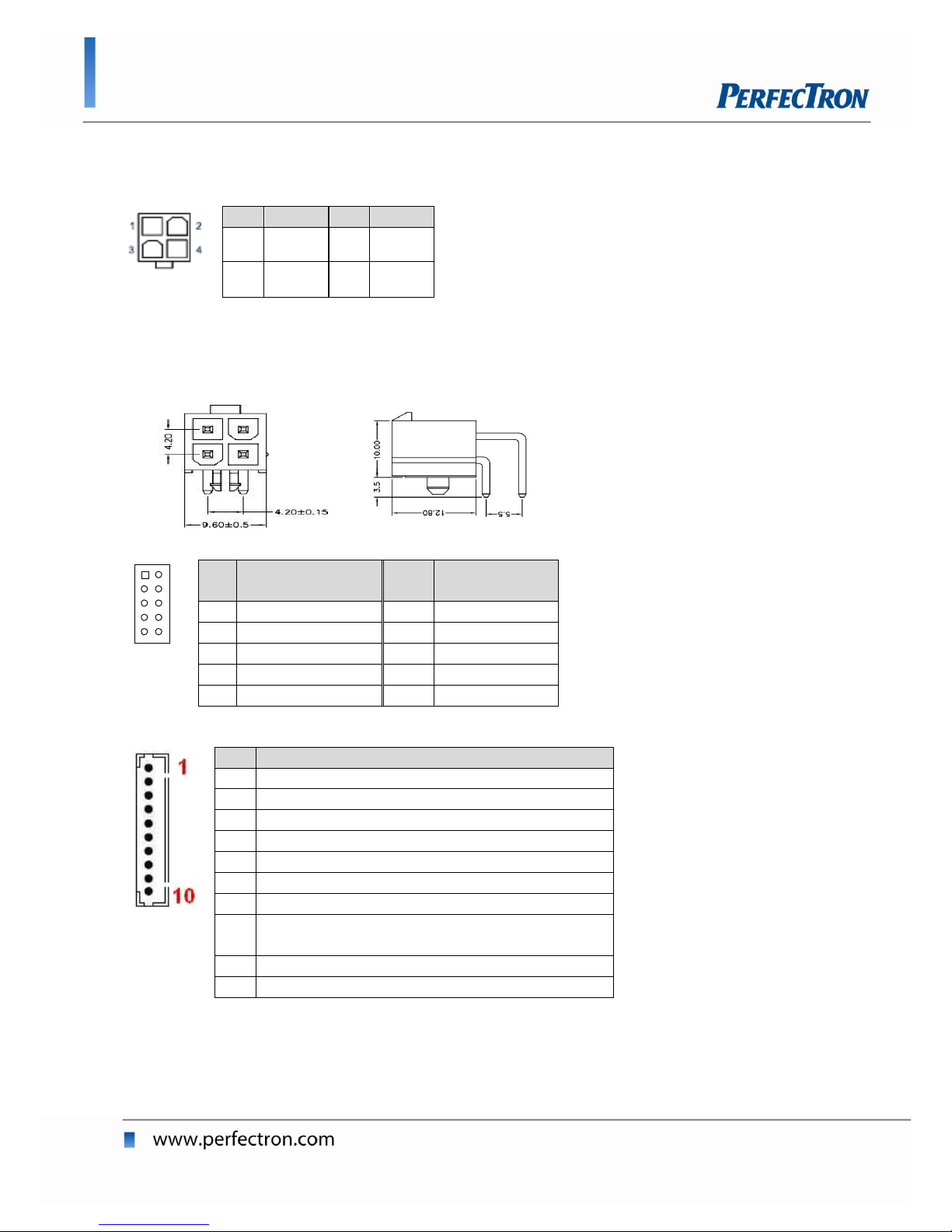
ATX1 DC Power Input Connector
Pin
Signal
Pin
Signal
1
GND
2
GND
3
+12V
4
+12V
2x2 pin power connector with 90 degrees (Optional feature for
OXY5313A/OXY5315A)
Digital I/O Pin Header
2
109
1
Pin Signal
Pin
Signal
1
Digital Output 0
2
Digital Input 0
3
Digital Output 1
4
Digital Input 1
5
Digital Output 2
6
Digital Input 2
7
Digital Output 3
8
Digital Input 3
9
+5V
10
GND
COM2~4 RS-232 Port (1x10 pin Wafer)
Pin
Signal
1
DCD, Data carrier detect
2
DSR, Data set ready
3
RXD, Receive data
4
RTS, Request to send
5
TXD, Transmit data
6
CTS, Clear to send
7
DTR, Data terminal ready
8
RI, Ring indicator (Can choose +5V or
+12V )
9
GND, ground
10
+5V
Page 15
OXY5313A 3.5” SBC User’s Manual
15
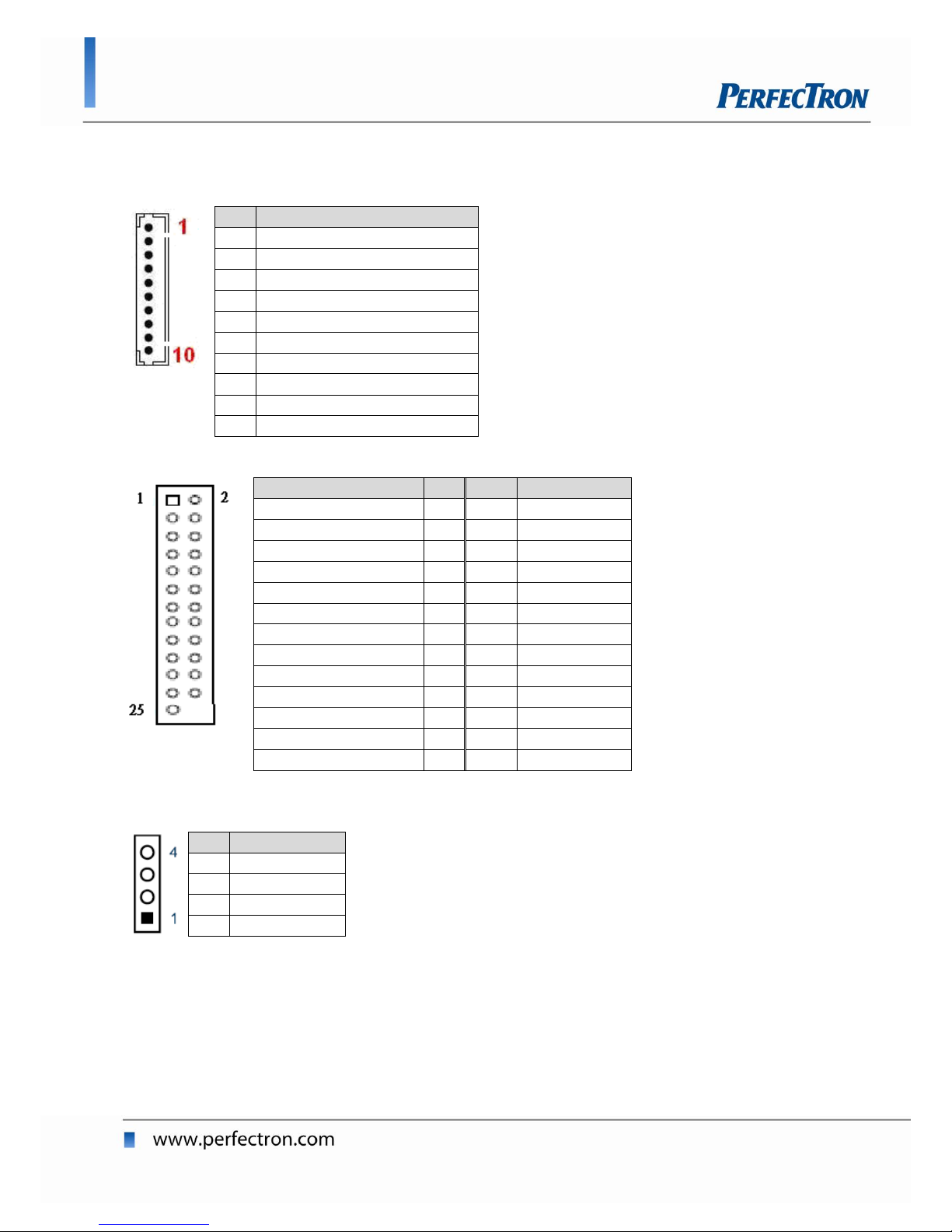
COM5~8 RS-232 Port Wafer
Pin
Signal
1
DCD, Data carrier detect
2
DSR, Data set ready
3
RXD, Receive data
4
RTS, Request to send
5
TXD, Transmit data
6
CTS, Clear to send
7
DTR, Data terminal ready
8
RI Ring
9
GND, ground
10
+5V
LPT1 Parallel Port Pin Header
Signal
Pin
Pin
Signal
Line printer strobe
1 2 AutoFeed
PD0, parallel data 0
3 4 Error
PD1, parallel data 1
5 6 Initialize
PD2, parallel data 2
7 8 Select In
PD3, parallel data 3
9
10
Ground
PD4, parallel data 4
11
12
Ground
PD5, parallel data 5
13
14
Ground
PD6, parallel data 6
15
16
Ground
PD7, parallel data 7
17
18
Ground
ACK, acknowledge
19
20
Ground
Busy
21
22
Ground
Paper empty
23
24
Ground
Select
25
SPD/IF output pin Header
Pin
Signal Name
1
SPDIF_IN
2
GND
3
SPDIF_OUT
4
GND
Page 16
OXY5313A 3.5” SBC User’s Manual
16
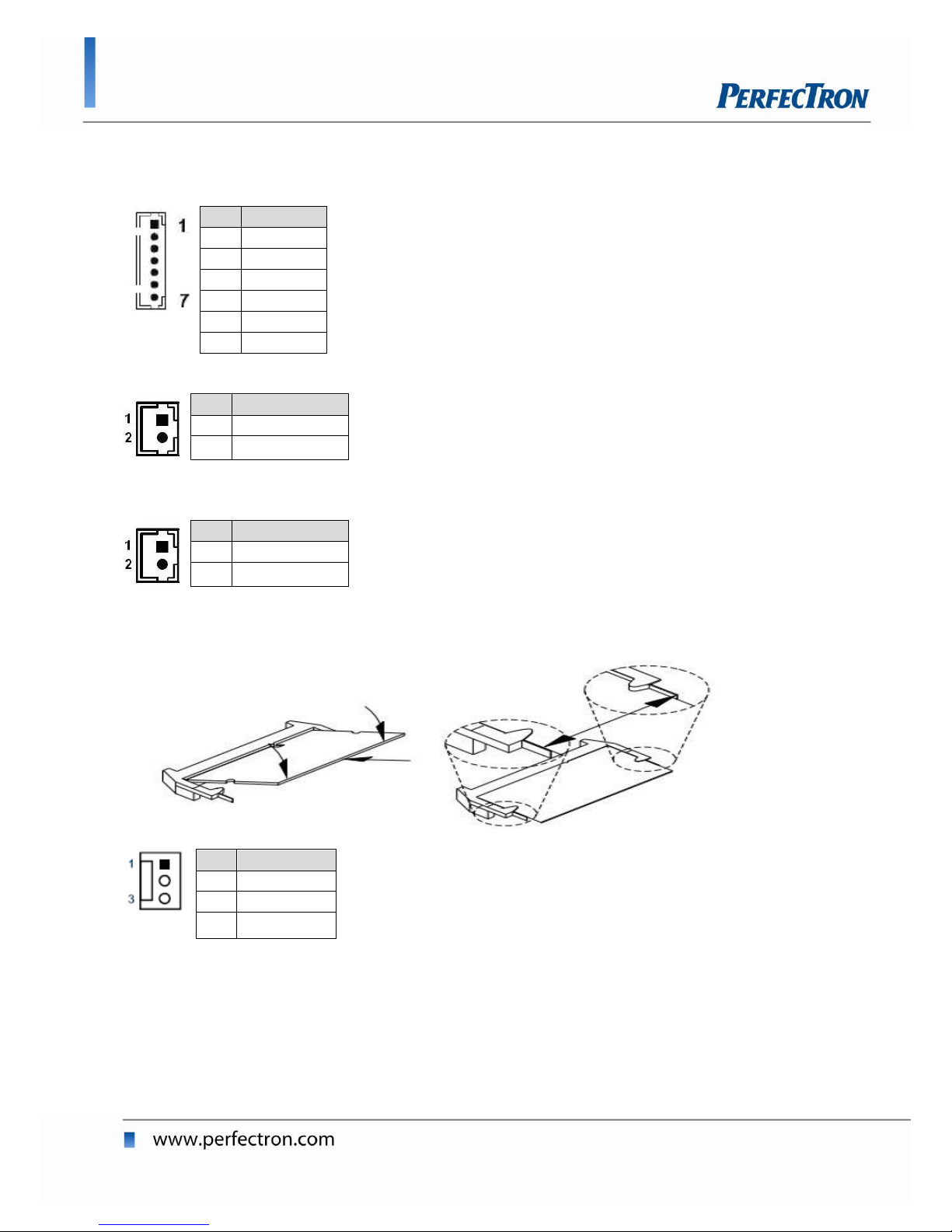
AUDIO1 Audio Output Wafer
Pin
Signal
1
LOUT_R
2
GND
3
LOUT_L
4
LIN_R
5
MIC
6
LIN_L
AMP_R1 Audio AMP Right Output Wafer
Pin
Signal Name
1
Speaker+
2
Speaker-
AMP_L1 Audio AMP Left Output Wafer
Pin
Signal Name
1
Speaker+
2
Speaker-
DDR3_1 DDR3 Memory DIMM Slot
CPU/System FAN
Pin
Signal
1
GND
2
+12V
3
FAN_RPM
Page 17
OXY5313A 3.5” SBC User’s Manual
17
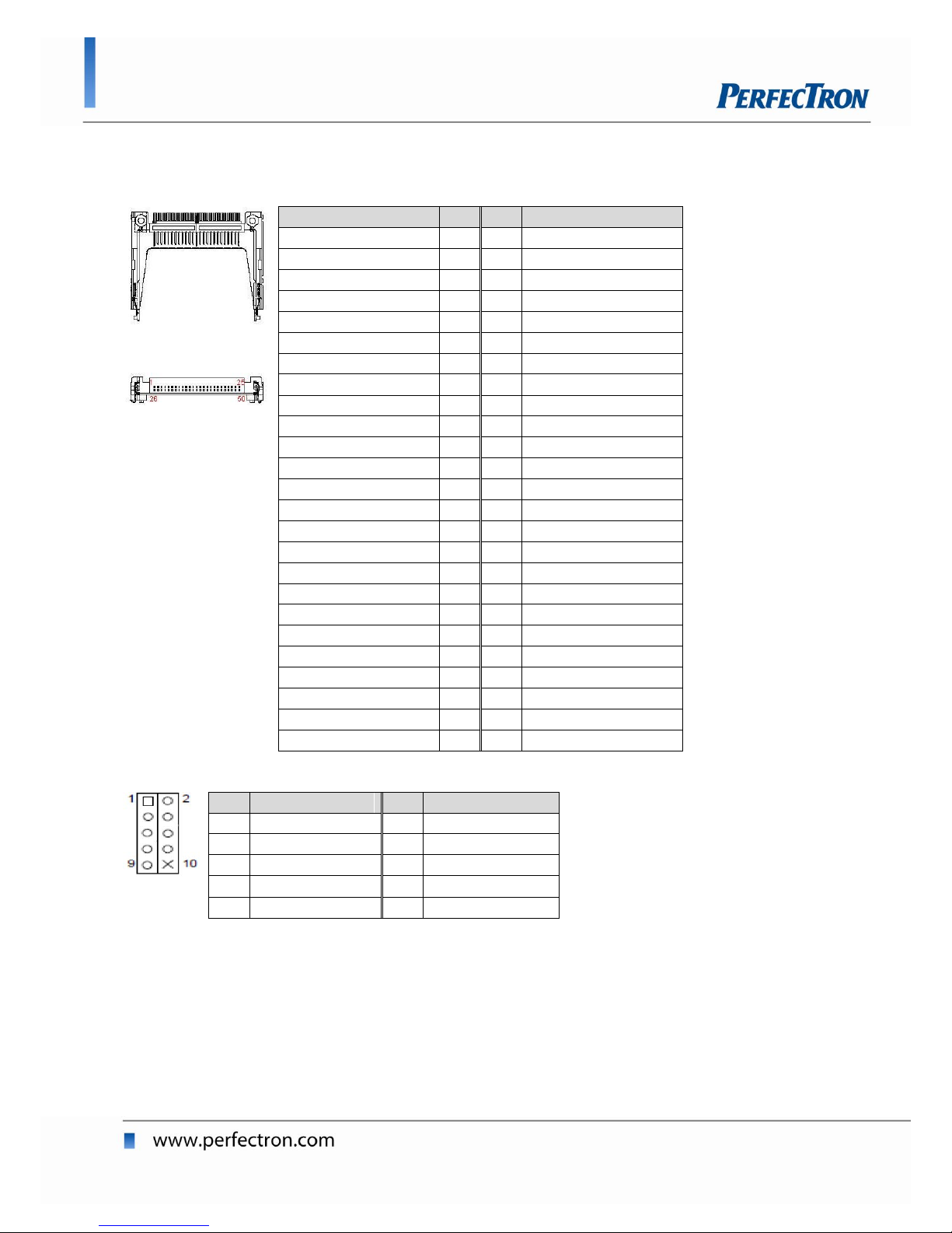
FD1 CF Type II Connector
Signal Name
Pin
Pin
Signal Name
GND
1
26
GND
IDE Data 3
2
27
IDE Data 11
IDE Data 4
3
28
IDE Data 12
IDE Data 5
4
29
IDE Data 13
IDE Data 6
5
30
IDE Data 14
IDE Data 7
6
31
IDE Data 15
IDE Chip select 1#
7
32
IDE Chip select 3#
GND
8
33
GND
GND
9
34
IDEIOR#
GND
10
35
IDEIOW#
GND
11
36
+5V
GND
12
37
IDEIRQ
+5V
13
38
+5V
GND
14
39
PCSEL
GND
15
40
NC
GND
16
41
Reset IDE
GND
17
42
IDEIORDY
SDA2
18
43
DREQ
IDE Address 1
19
44
DACK#
IDE Address 0
20
45
IDE activity
IDE Data 0
21
46
PDIAG#
IDE Data 1
22
47
IDE Data 8
IDE Data 2
23
48
IDE Data 9
IOIS16#
24
49
IDE Data 10
GND
25
50
GND
FP1 Front Panel 1 Pin Header
Pin
Signal
Pin
Signal
1
HDD LED +
2
Power LED +
3
HDD LED -
4
Power LED -
5
Reset Button -
6
Power Button +
7
Reset Button +
8
Power Button -
9 10
NC
Page 18
OXY5313A 3.5” SBC User’s Manual
18
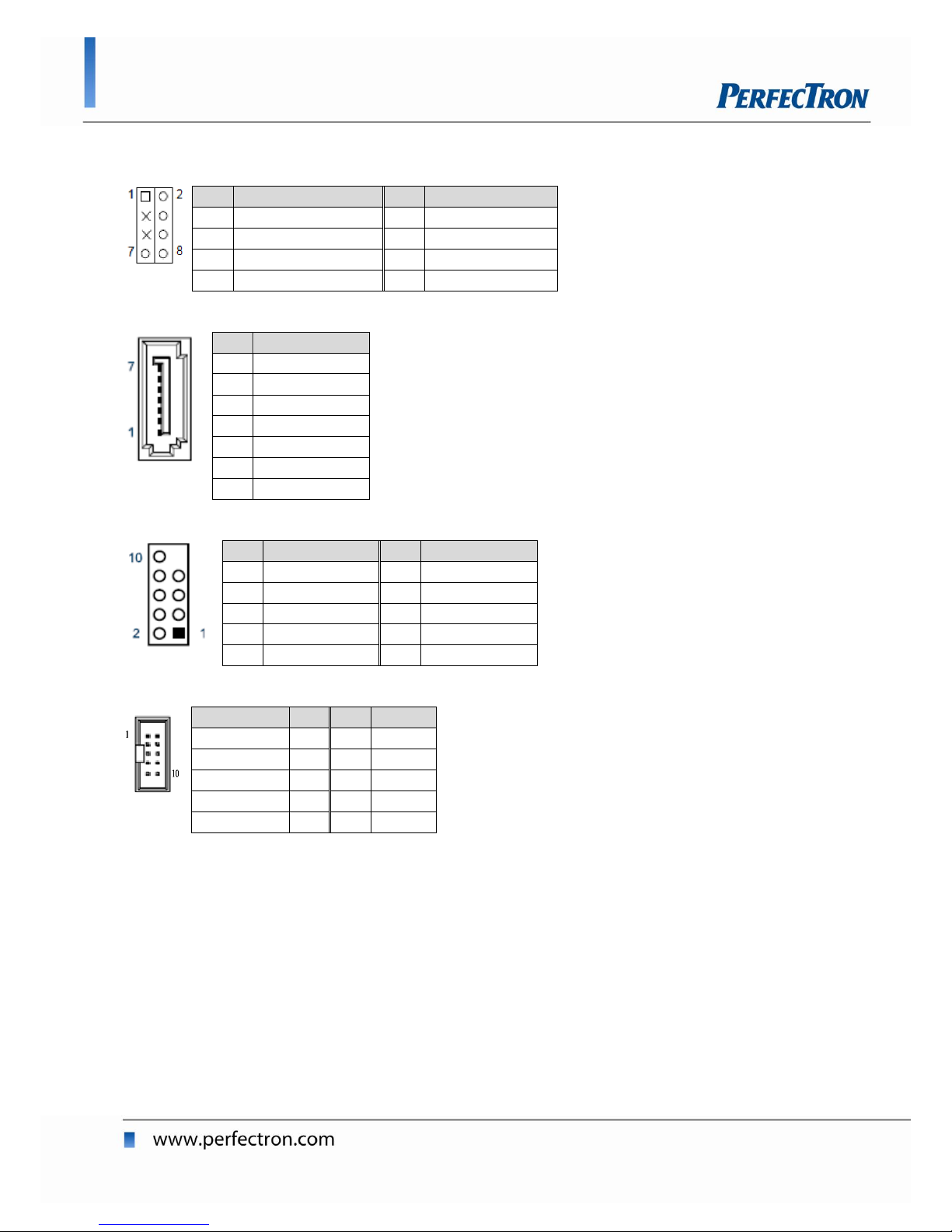
FP2 Front Panel 2 Pin Header
Pin
Signal
Pin
Signal
1
Speaker +
2
SMBus Clock
3
NC 4 SMBus Data -
5
Internal Speaker-
6
GND
7
Speaker -
8
Keyboard Lock
SATAI1, SATA2 Serial ATA 2.0 Connector
Pin
Signal Name
1
GND
2
TX+
3
TX-
4
GND
5
RX-
6
RX+
7
GND
USB2,USB3,USB4 USB2.0 Pin Header
Pin
Signal Name
Pin
Signal Name
1
+5V
2
+5V
3
USB_A-
4
USB_B-
5
USB_A+
6
USB_B+
7
GND
8
GND
9
KEY
10
GND
JTAG1 TAG Port Box Header
Signal
Pin
Pin
Signal
ITP_TCK
1 2 +3.3V
ITP_TMS
3 4 GND
ITP_TDI
5 6 GND
ITP_TDO
7 8 GND
ITP_RST#
9
10
NC
Page 19
OXY5313A 3.5” SBC User’s Manual
19
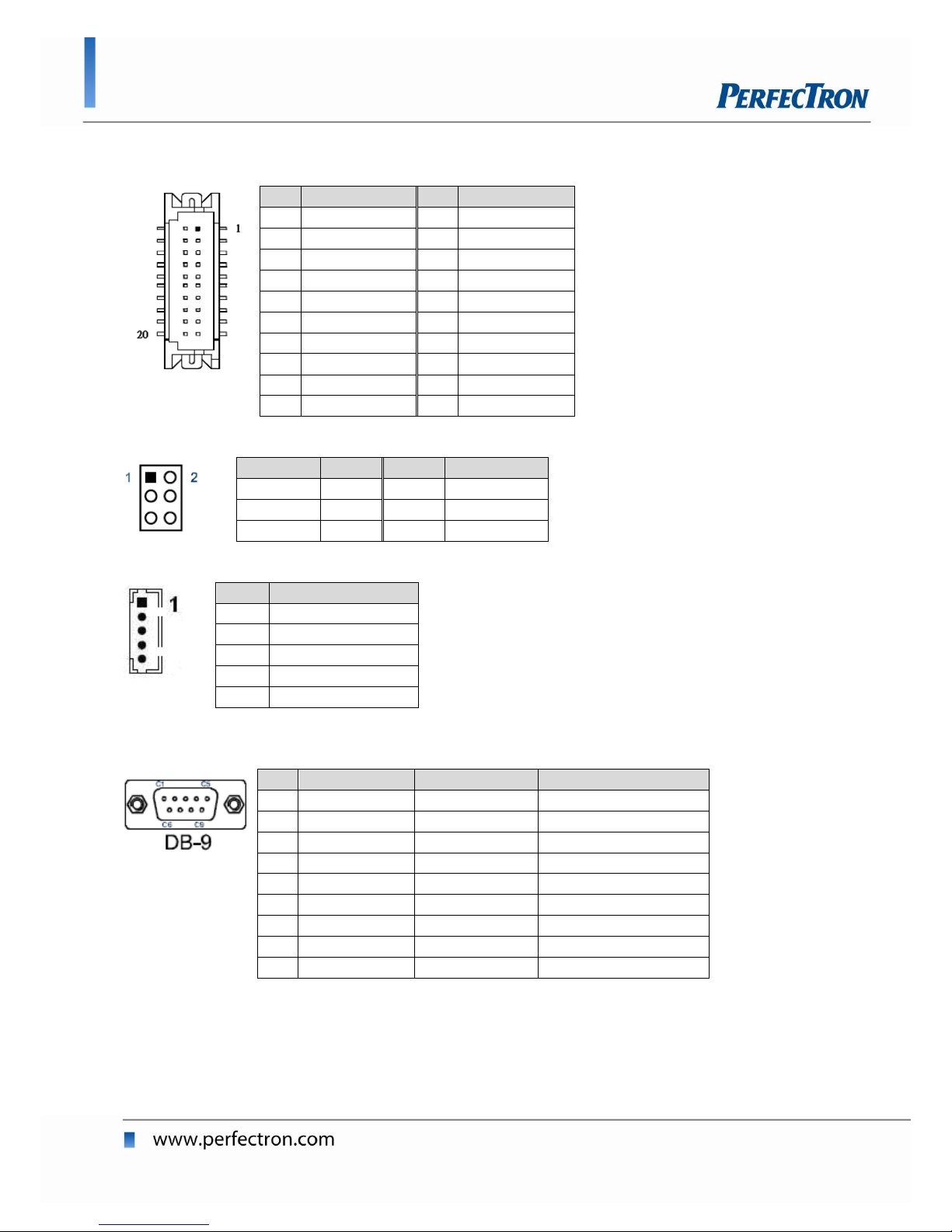
JLVDS1 18 bit LVDS Panel Connector
Pin
Signal Name
Pin
Signal Name
2
+5V
1
+3.3V
4
+5V
3
+3.3V
6
LVDS_A0-
5
LVDS_A1-
8
LVDS_A0+
7
LVDS_A1+
10
GND
9
GND
12
LVDS_A2-
11
LVDS_CLK-
14
LVDS_A2+
13
LVDS_CLK+
16
GND
15
GND
18
DDC_DAT
17
+12V
20
DDC_CLK
19
+12V
KBMS1 KB/MS Pin Header
Signal
Pin
Pin
Signal
VCC
1 2 KBDAT
MSDAT
3 4 KBCLK
MSCLK
5 6 GND
JBKL1 Panel Backlight Wafer
Pin
Signal Name
1
+12V
2
GND
3
BL_EN
4
BL_ADJ
5
+5V
COM1 (RS-232/422/485 Port A DB-9 Connector)
Pin
RS-232
RS-422
Half Duplex RS-485
1
DCD
TX-
DATA-
2
RXD
RX+
NA 3 TXD
TX+
DATA+
4
DTR
RX-
NA 5 GND
GND
GND
6
DSR
NA
NA 7 RTS
NA
NA 8 CTS
NA
NA 9 +5V/+12V/RI
+5V/+12V/NA
+5V/+12V/NA
Page 20
OXY5313A 3.5” SBC User’s Manual
20
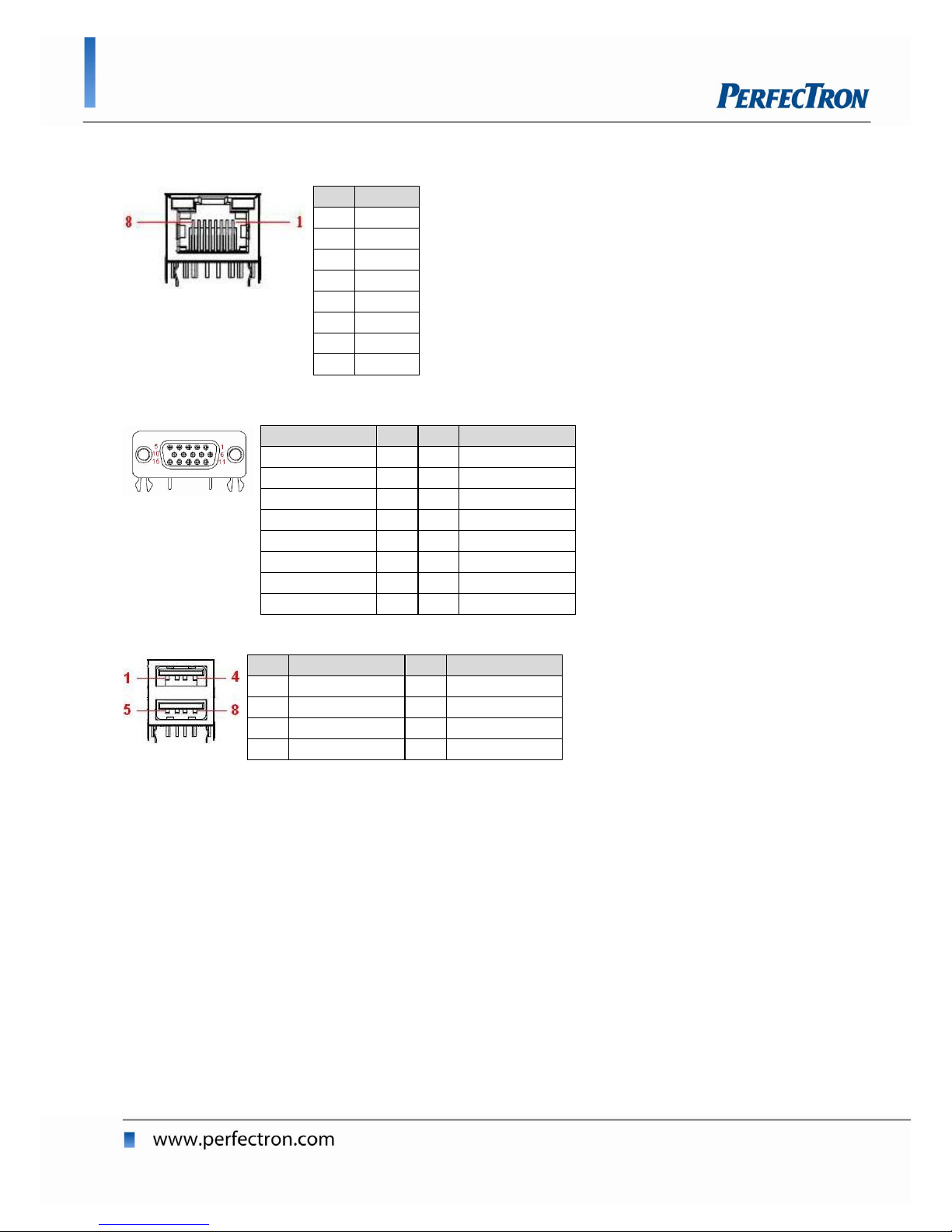
LAN1 , LAN2 10/100/1000 Ethernet RJ-45 Connector
Pin
Signal
1
Tx+
2
Tx- 3 Rx+
4
NC 5 NC 6 Rx-
7
NC 8 NC
VGA1 CRT DB-15 Connector
Signal Name
Pin
Pin
Signal Name
Red
1 2 Green
Blue
3 4 NC
GND
5 6 GND
GND
7 8 GND
VCC
9
10
GND
NC
11
12
DDC data
HSYNC
13
14
VSYNC
DDC clock
15
USB1 2-Stack USB2.0 Type A Connector
Pin
Signal Name
Pin
Signal Name
1
+5V
5
+5V
2
USB1-
6
USB0-
3
USB1+
7
USB0+
4
GND
8
GND
Page 21
OXY5313A 3.5” SBC User’s Manual
21
Chapter 3: Getting St arted
This chapter provides information on how to install components to the
OXY5313A. Specifically, the installation of memory modules and operating
system are explained.
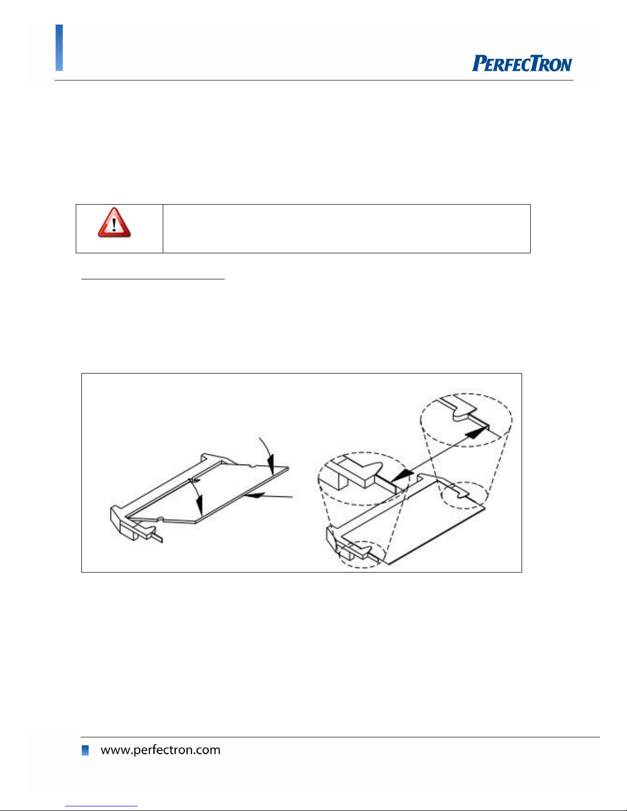
3.1 Installing System Memory
The OXY5313A supports DDR3 800 SO-DIMM.
Disconnect all power supplies to the board before installing a memory
module to prevent damage to the board and memory module.
To install a memory module:
1. Located the memory module slots on the motherboard.
2. Push the socket retaining clips outward to unlock the slots.
3. Align the memory module with the socket to make sure the notch aligns
with the slot key on the socket.
4. Insert the module firmly into the desired slot until the retaining clips lock
and secure the memory module.
3.2 installing the CF card
The OXY5313A built-in CF Type II Socket
Step 1: Locate the CF card socket. Locate the CompactFlash® slot.
Step 2: Align the CF card. Align the CompactFlash® card. The label side should be
facing away from the board. The grooves on the CompactFlash® slot ensure
that the card cannot be inserted the wrong way.
Step 3: Insert the CF card. Push until the CompactFlash® card is firmly seated in the
slot
Page 22

OXY5313A 3.5” SBC User’s Manual
22
3.3 Driver Installation
The OXY5313A drivers for Windows XP 32-bit are located in the following
directories on the Driver CD or can be downloaded from the Perfectron
website (http://www.perfectron.com):
Follow the instructions below to install the required OXY5313A drivers:
1. Install the Windows operating system before installing any drivers. Most
standard I/O device drivers are installed during Windows installation.
2. Install the chipset driver by running the program
X:\OXY5313A Driver\INF\setup.exe. Follow the provided instructions and
reboot the computer when instructed.
3. Install the display driver and utilities by running the program
X:\OXY5313A Driver\VGA\WIN2KXP_32\setup.exe. Follow the provided
instructions and reboot the computer when instructed.
4. Install the LAN driver by running the program
X:\OXY5313ADriver\LAN\Windows\2000_XP_2003
Server\PRO2KXP.exe. Follow the provided instructions and reboot the
computer, if is required.
5. Install the Audio driver by running the program
X:\OXY5313A Driver\Audio\32bit\2K_XP\setup.exe. Follow the provided
instructions and reboot the computer, if required.
Chipset X:\OXY5313A Driver\INF
Display X:\OXY5313A Driver\VGA\WIN2KXP_32
LAN X:\OXY5313A Driver\LAN\Windows\2000_ XP_2003 Server
Audio X:\OXY5313A Driver\Audio\32bit\2K_XP
Page 23
OXY5313A 3.5” SBC User’s Manual
23
Chapter 4: AMI BIOS UTILITY
This chapter provides users with detailed descriptions on how to set up a
basic system configuration through the AMIBIOS8 BIOS setup utility.
4.1 Starting
To enter the setup screens, perform the following steps:
Turn on the computer and press the <Del> key immediately.
After the <Del> key is pressed, the main BIOS setup menu displays.
Other setup screens can be accessed from the main BIOS setup menu,
such as the Chipset and Power menus.
4.2 Navigation Keys
The BIOS setup/utility uses a key-based navigation system called h ot key s.
Most of the BIOS setup utility hot keys can be used at any time during the
setup navigation process.
Some of the hot keys are <F1>, <F10>, <Enter>, <ESC>, and <Arrow> keys.
Some of the navigation keys may differ from one screen to another.
Å Left/Right
The Left and Right <Arrow> keys moves the cursor to select a
menu.
ÇÈ Up/Down
The Up and Down <Arrow> keys moves the cursor to select a
setup screen or sub-screen.
+− Plus/Minus
The Plus and Minus <Arrow> keys changes the field value of a
particular setup setting.
Tab
The <Tab> key selects the setup fields.
F1
The <F1> key displays the General Help screen.
F10
The <F10> key saves any changes made and exits the BIOS
setup utility.
Esc
The <Esc> key discards any changes made and exits the BIOS
setup utility.
Enter
The <Enter> key displays a sub -screen or changes a selected or
highlighted option in each menu.
Page 24
OXY5313A 3.5” SBC User’s Manual
24
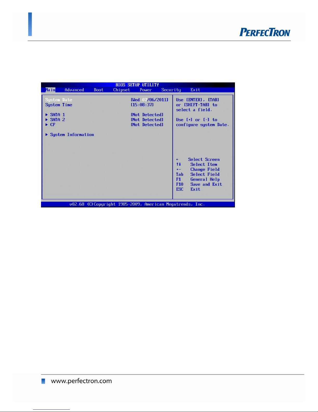
4.3 Main Menu
The Main menu is the screen that first displays when BIOS Setup is entered,
unless an error has occurred.
You could setup these items on the Main menu:
System T i m e : S e l e c t t h i s o p t i o n t o s e t t h e s y s t e m
t i m e .
S y s t e m Date: Select this option to set the system date.
CF: S e l e c t t h i s o p t i o n t o s e t t h e p a r a m e t e r s .
S ys t e m I n f o r m a t i o n : S e l e c t t h i s o p t i o n t o d i s p l a y
s y s t e m i n f o r m a t i o n .
Use the <Arrow> keys to enter the appropriate time and date.
Press the <Tab> key or the <Arrow> keys to move between fields.
The date s e t t in g must be entered in MM/DD/YY format. The time
se t t i ng is entered in HH:MM:SS format.
Page 25
OXY5313A 3.5” SBC User’s Manual
25
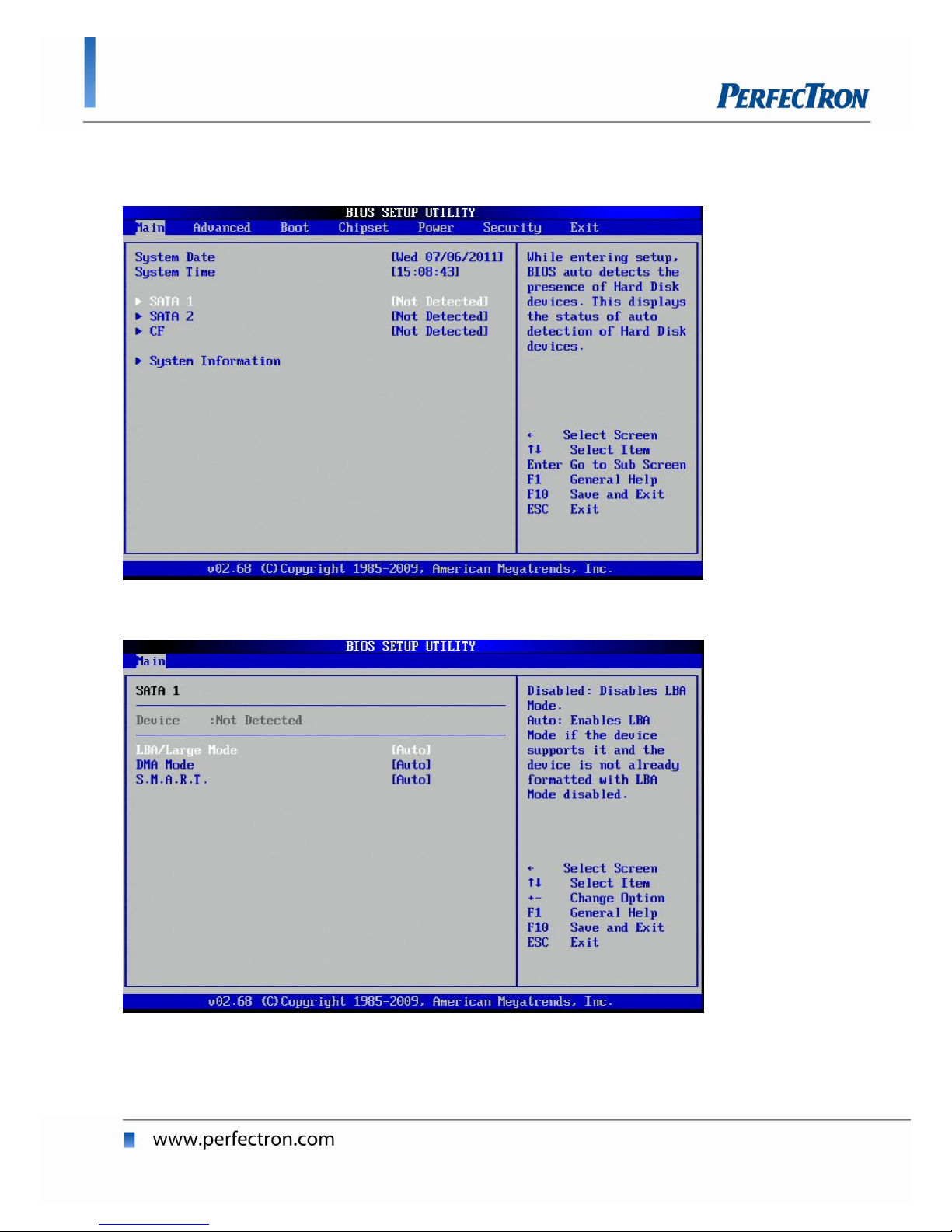
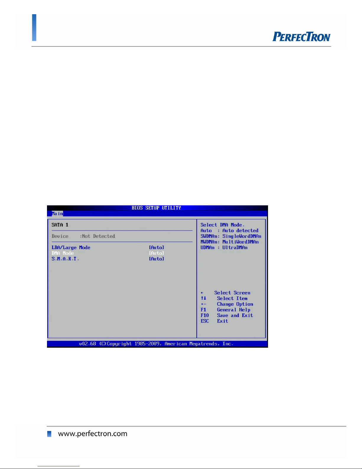
SATA 1 Setup
BIOS will automatically detect the presence of a SATA HDD.
SATA 1(LBA/Large Mode)
Page 26
OXY5313A 3.5” SBC User’s Manual
26
In order for LBA to work, it must be supported by the BIOS and operating
system, but since it is also a new way of talking to the hard disk, the disk
must support it as well. All newer hard disks do in fact support LBA, and
when auto-detected by a BIOS supporting LBA, will be set up to use that
mode.
A drive using LBA is not subject to the 504 MiB disk size barrier, however
there has been a great deal of confusion regarding LBA and what it does. In
particular, a lot of people think that it is the LBA addressing that "gets around
the 504 MB barrier".
LBA from the BIOS doesn't affect newer OSs such as Linux, or NT/2000,
because these OSs bypass the BIOS services and make their own direct
LBA calls.
(The default BIOS setting for LBA/Large mode is Auto)
SATA 1(DMA Mode)
(The default BIOS setting for DMA mode is Auto)
Page 27
OXY5313A 3.5” SBC User’s Manual
27
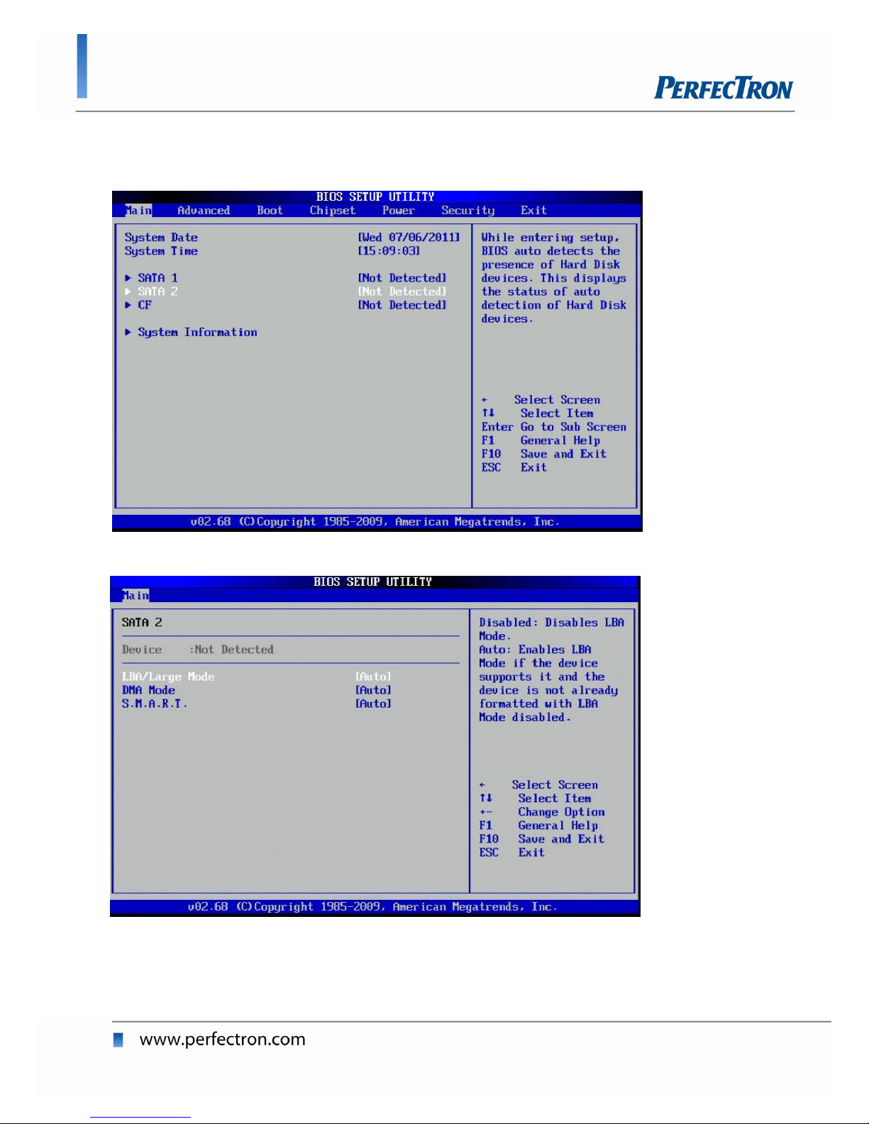
SATA 2 Setup
BIOS will automatically detect the presence of a SATA HDD
SATA 2(LBA/Large Mode)
(The default BIOS setting for LBA/Large Mode is Auto)
Page 28
OXY5313A 3.5” SBC User’s Manual
28
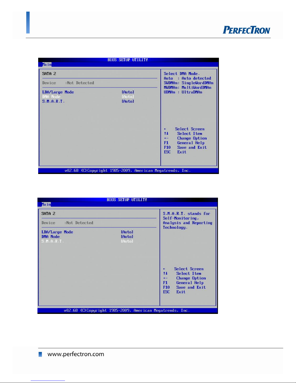
SATA 2(LBA/Large Mode)
(The default BIOS setting for DMA mode is Auto)
S.M.A.R.T for SATA 2
(The default BIOS setting for S.M.A.R.T is Auto)
Page 29
OXY5313A 3.5” SBC User’s Manual
29
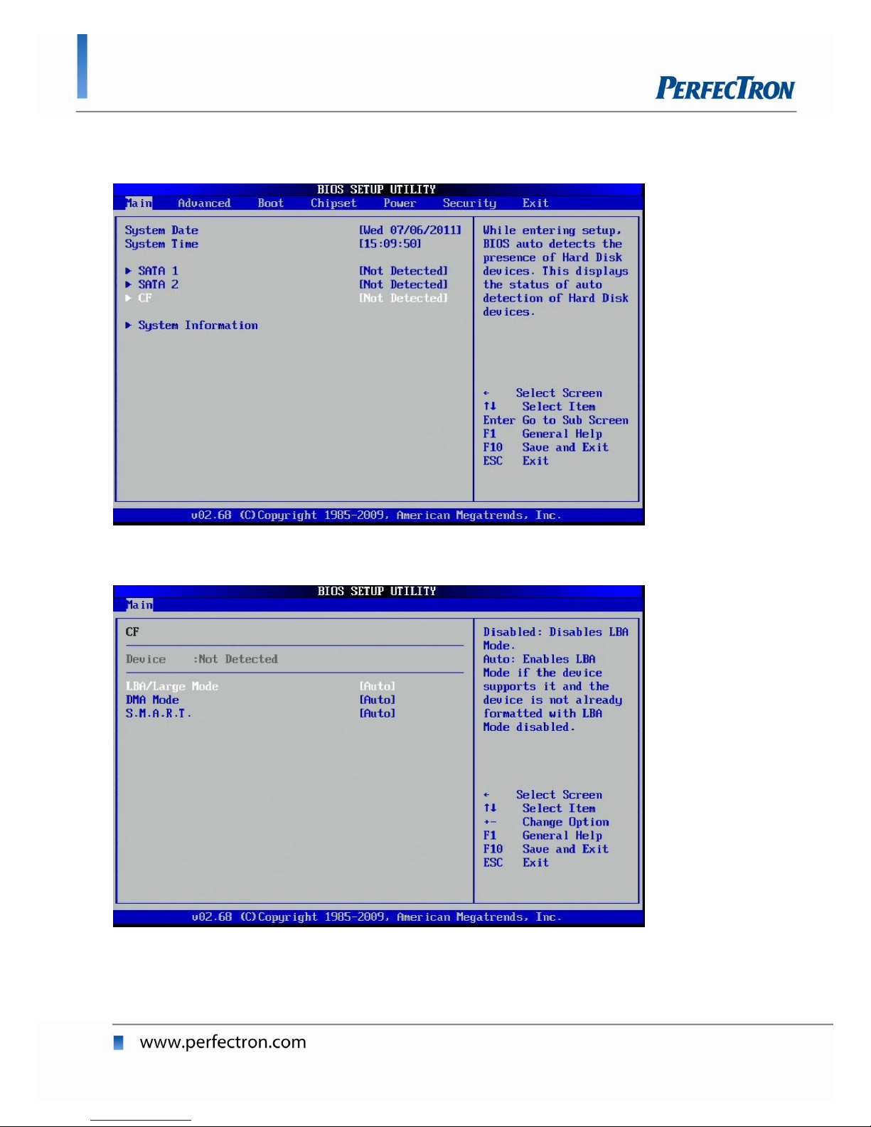
CF Setup
BIOS will automatically detect the presence of a CF card
CF setup(LBA/Large Mode)
(The default BIOS setting for LBA/Large mode is Auto)
Page 30
OXY5313A 3.5” SBC User’s Manual
30
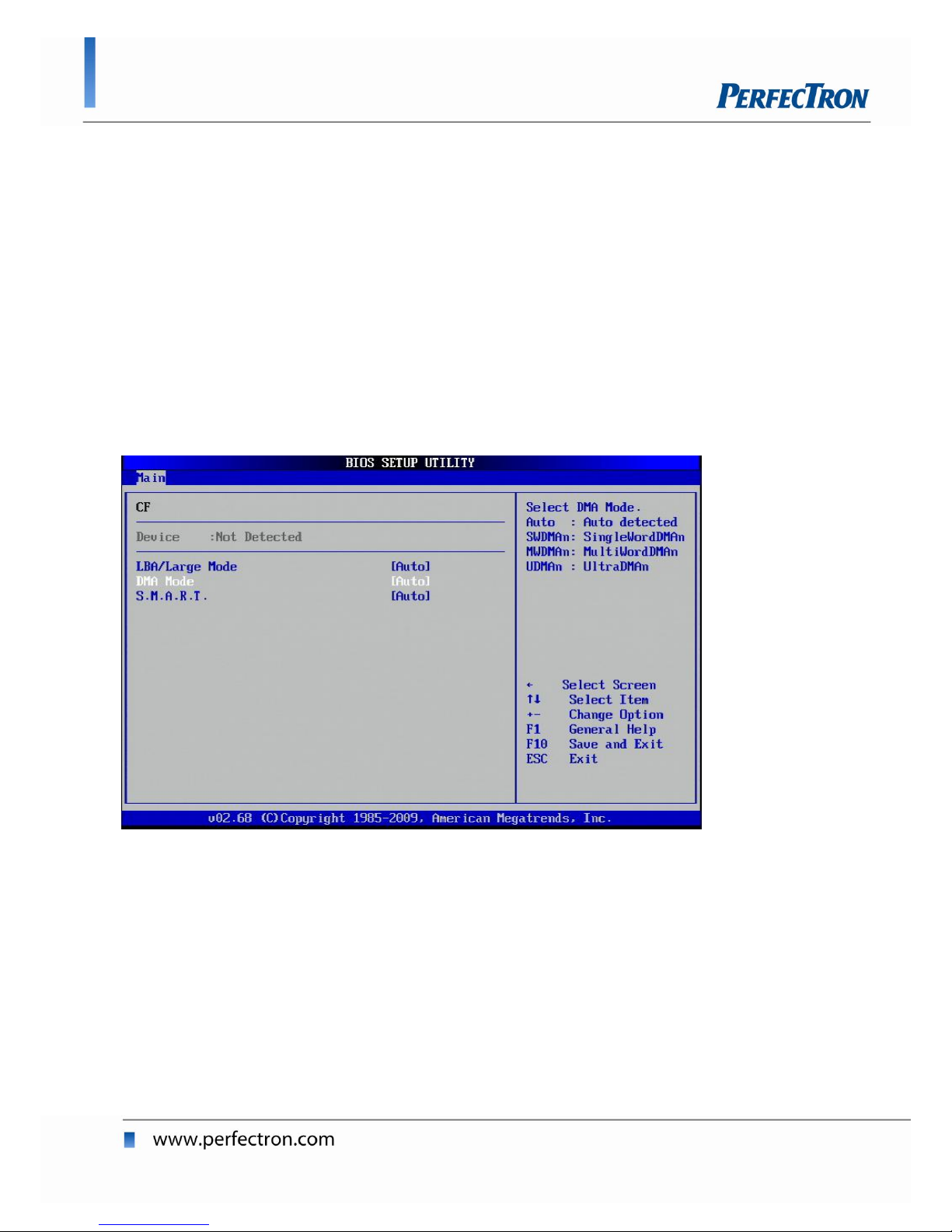
CF (DMA Mode)
DMA (Direct memory access) mode is a high performance mode for
transferring data to and from devices, The burner devices can function in
either DMA or PIO modes. DMA mode allows the processor to transfer large
pieces of data with very little software overhead - therefore requiring low
CPU utilization. In this mode, high speed burning can be performed in
background with other programs running.PIO mode requires CPU
processing for every few bytes sent to the device, so that CPU utilization
becomes very high when trying to burn at high speeds.
Page 31
OXY5313A 3.5” SBC User’s Manual
31
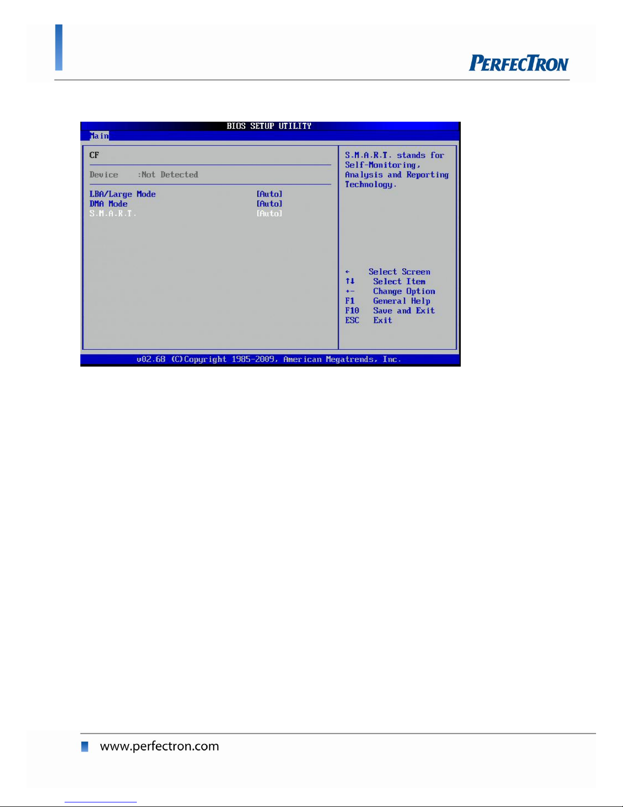
S.M.A.R.T for CF
S.M.A.R.T. ( Self-Monitoring, Analysis and Reporting Technology;
sometimes written as SMART) is a monitoring system for computer hard
disk drives to detect and report on various indicators of reliability, in the hope
of anticipating failures.
When a failure is anticipated by S.M.A.R.T., the user may choose to replace
the drive to avoid unexpected outage and data loss. The manufacturer may
be able to use the S.M.A.R.T. data to discover where faults lie and prevent
them from recurring in future drive designs
Page 32
OXY5313A 3.5” SBC User’s Manual
32
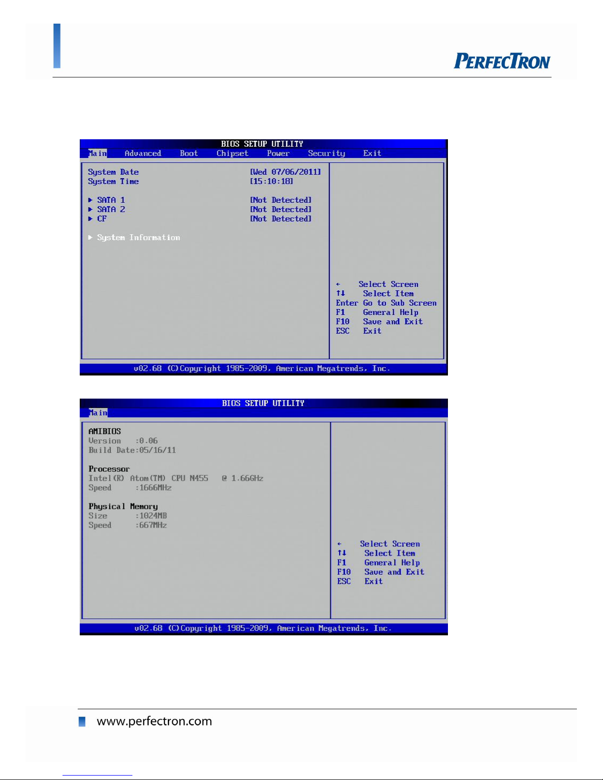
System Information
You can review the system information in the BIOS System Information
menu.
Page 33
OXY5313A 3.5” SBC User’s Manual
33
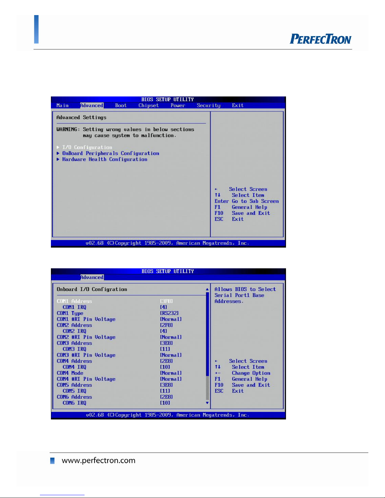
*OXY5313A contains an incorporated Intel D525 CPU onboard/OXY5315A
contains an incorporated Intel N455 CPU onboard*
4.4 Advanced Menu
Onboard I/O Configuration
Page 34
OXY5313A 3.5” SBC User’s Manual
34
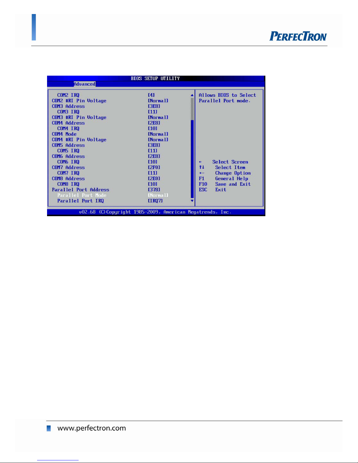
You could setup the IRQ and IRQ address for the OXY5315A. This line of
3.5” SBC supports 8xCOM Ports (COM1 Port belongs to D-Sub 9pin and
supports RS232/422/485. COM2~COM8 belongs to the 1x10 pin wafer
connector and supports RS232)
Page 35
OXY5313A 3.5” SBC User’s Manual
35
Onboard Peripherals Configuration
USB Function
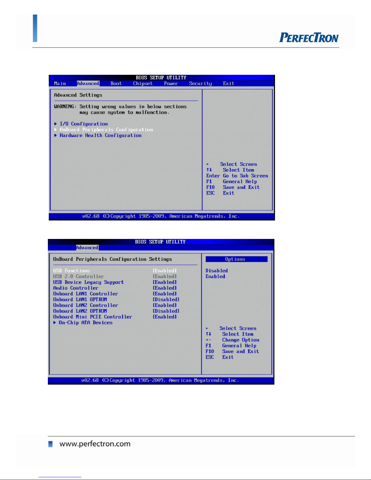
You could enable or disable the onboard USB functions and/or USB 2.0
Controller.
Page 36
OXY5313A 3.5” SBC User’s Manual
36
USB Device Legacy Support
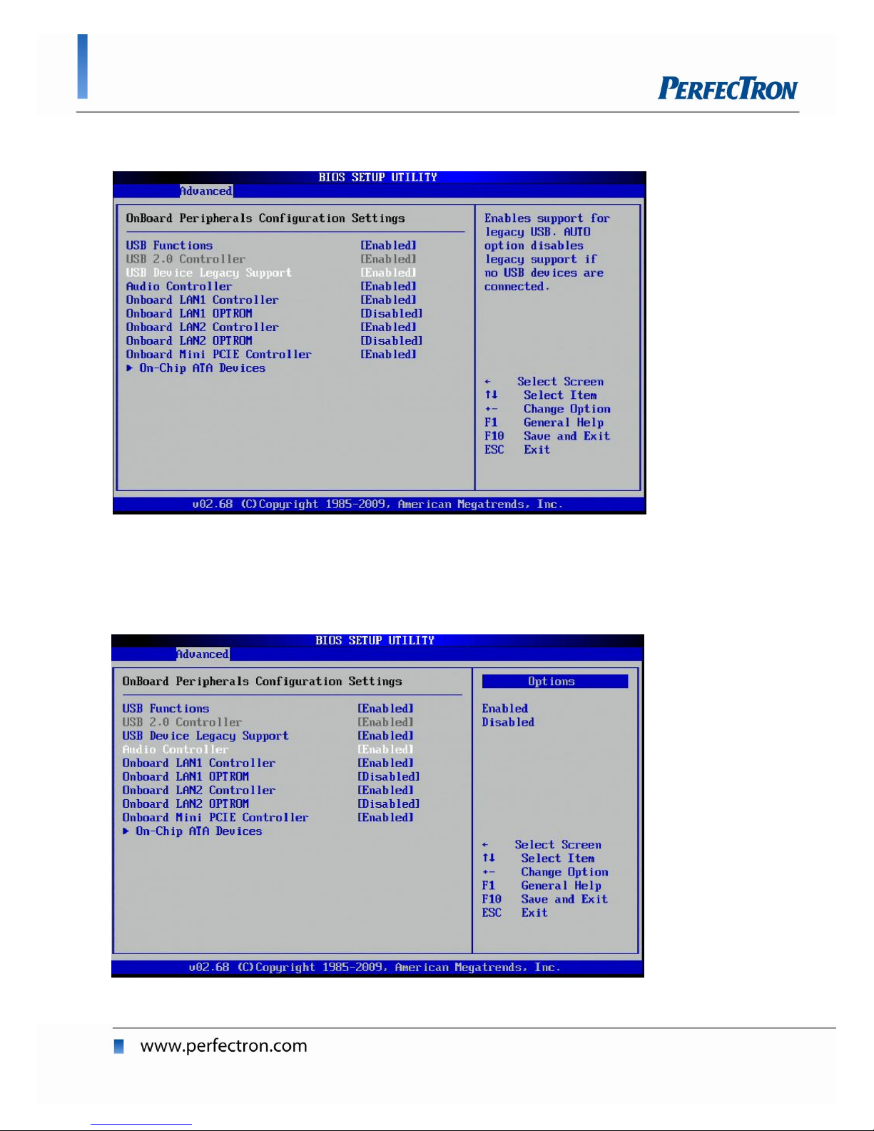
Legacy mode support is inherent to a system and is typically provided by
legacy hardware interface emulation.
Legacy mode support allows devices to function in an operating environment.
(The default BIOS setting for USB Legacy support is Enabled)
Audio Controller
Page 37
OXY5313A 3.5” SBC User’s Manual
37
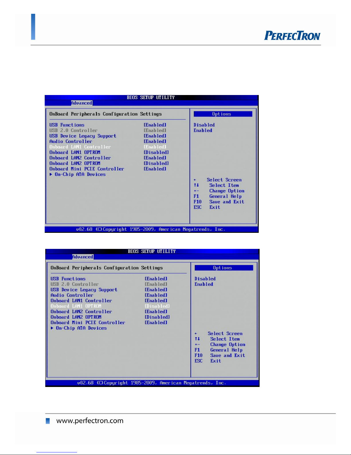
This setting enables or disables the onboard Audio Controller.
(The default BIOS setting for Audio Controller default is Enabled)
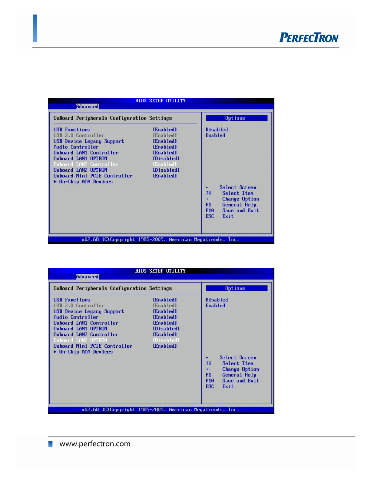
Onboard LAN1 Controller
This setting enables or disables the OnBoard LAN1 Controller.
Onboard LAN1 OPTROM
Page 38
OXY5313A 3.5” SBC User’s Manual
38
This setting enables or disables the Onboard LAN1 OPTROM setting.
(The default BIOS setting for Onboard LAN1 OPTROM is Disabled)
Onboard LAN2 Controller
This setting enables or disables the Onboard LAN2 Controller.
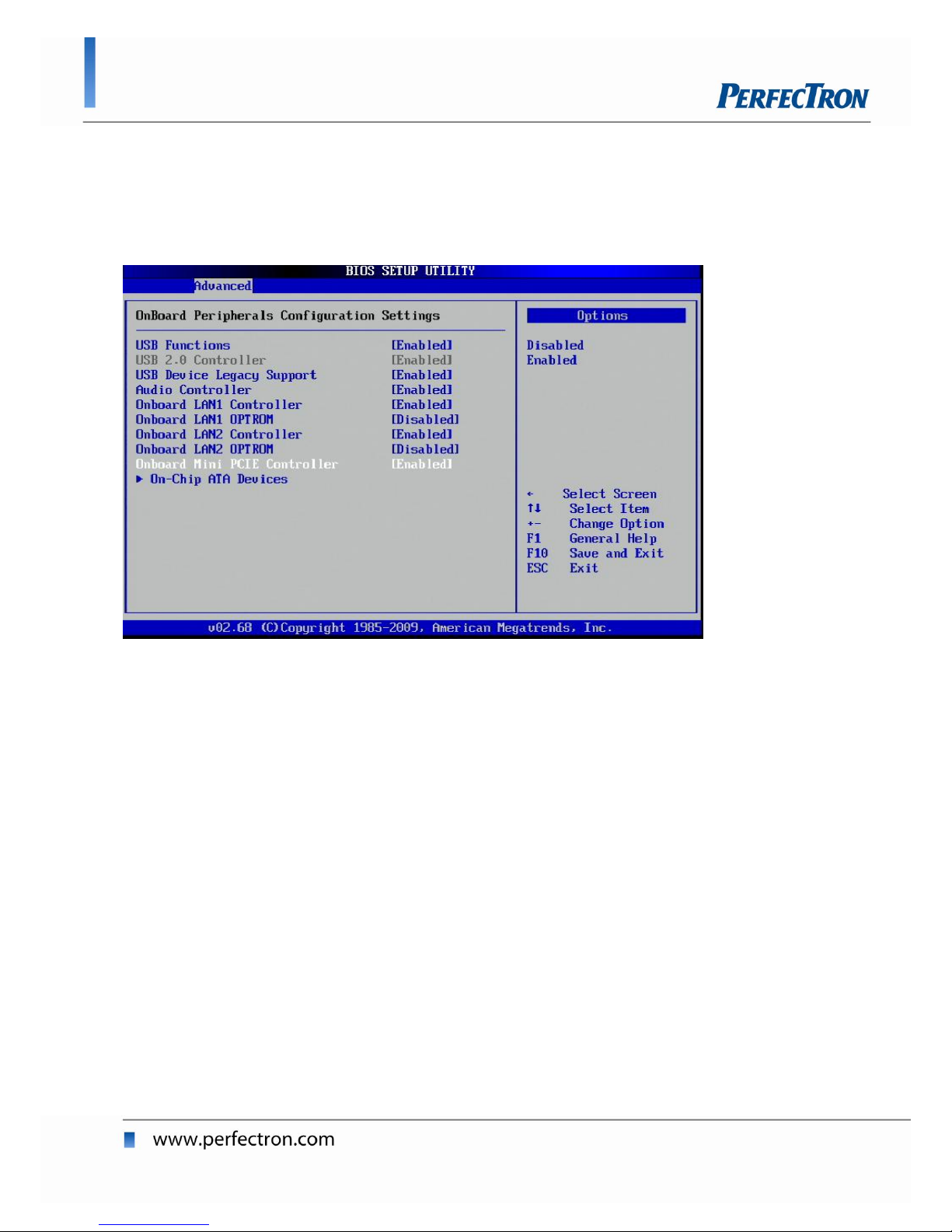
Onboard LAN2 OPTROM
Page 39
OXY5313A 3.5” SBC User’s Manual
39
This setting enables or disables the Onboard LAN2 OPTROM.
(The default BIOS setting is Disabled)
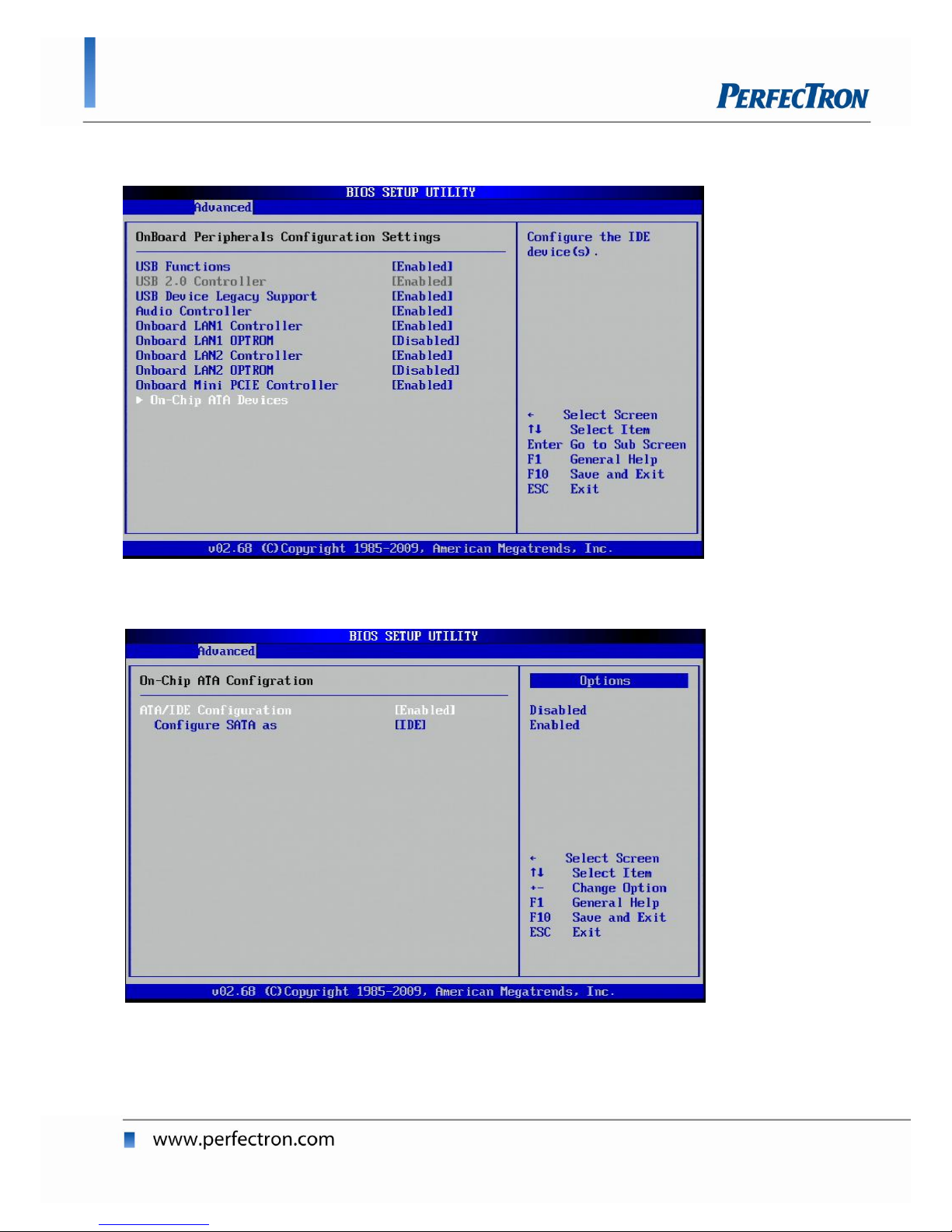
Onboard Mini-PCIE Controller
This setting enables or disables the Onboard Mini-PCIE Controller.
Page 40
OXY5313A 3.5” SBC User’s Manual
40
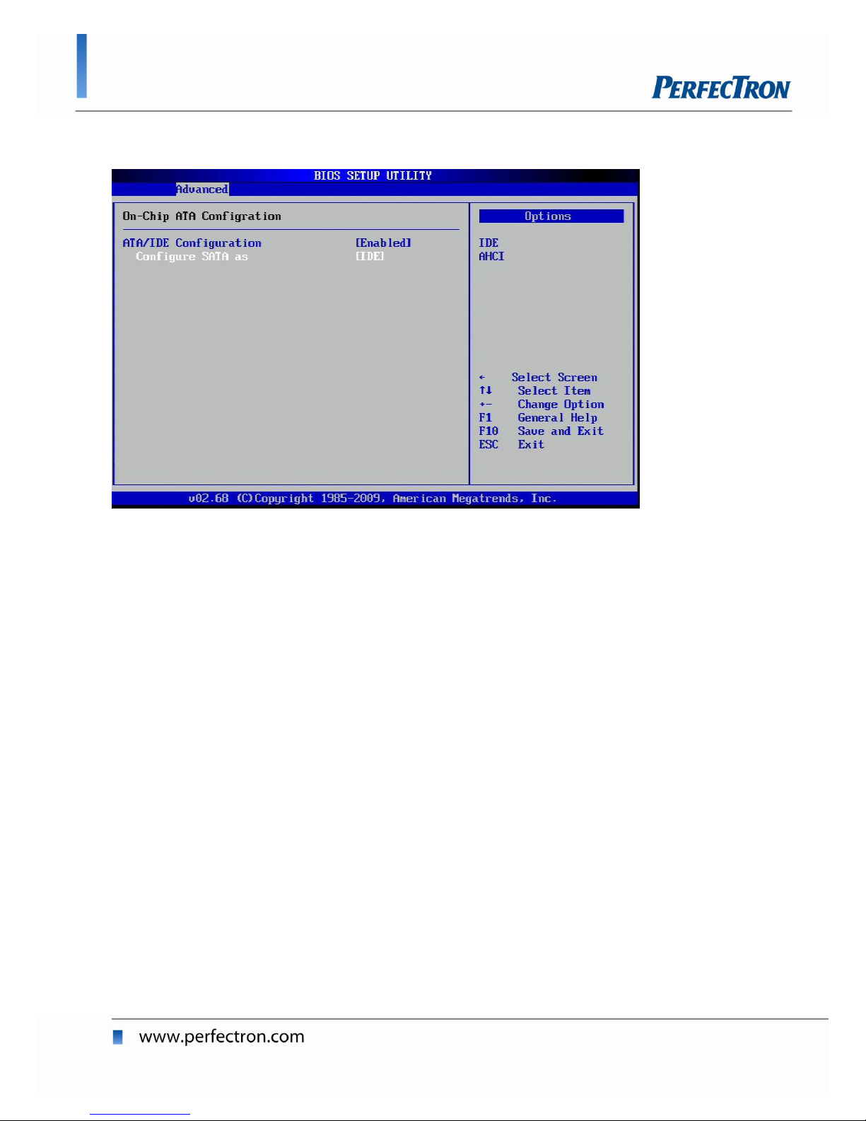
On-Chip ATA Devices
This setting contains two sub-menus. Press Enter to access the secondary
menu. The secondary menu has two settings:
ATA/IDE Configuration
This setting enables or disables the ATA/IDE Configuration.
Page 41
OXY5313A 3.5” SBC User’s Manual
41
Configure SATA as
This setting allows the most important peripheral equipment. The menu
options are: IDE and AHCI
*IDE: The function provides the bridge for the IDE to SATA hard disk drive
function.
*AHCI: This supports a SATA 3GB connection and supports NCQ and eSATA. *
Page 42
OXY5313A 3.5” SBC User’s Manual
42
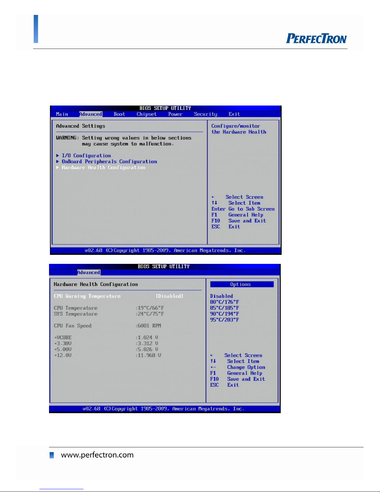
Hardware Health Configuration
The Hardware Health Configuration setting displays the system hardware
details such as CPU Warning Temperature, CPU Temperature, System
Temperature, CPU FAN speed, VCORE, +3.3V, +5V and +12V
Page 43
OXY5313A 3.5” SBC User’s Manual
43
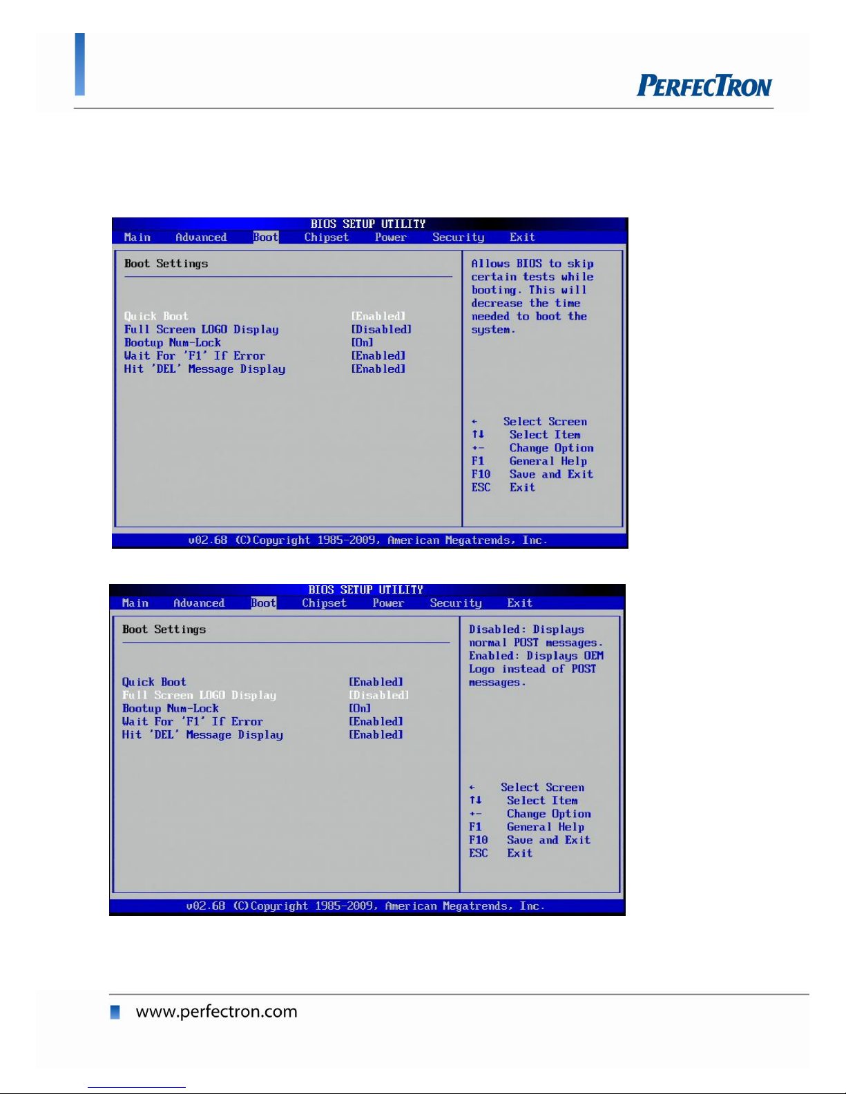
4.5 Boot Setting
The setting allows you to setup the Boot sequence for a 3.5” SBC.
Quick Boot
(The default BIOS setting is Enabled)
Full Screen Logo Display
Page 44
OXY5313A 3.5” SBC User’s Manual
44
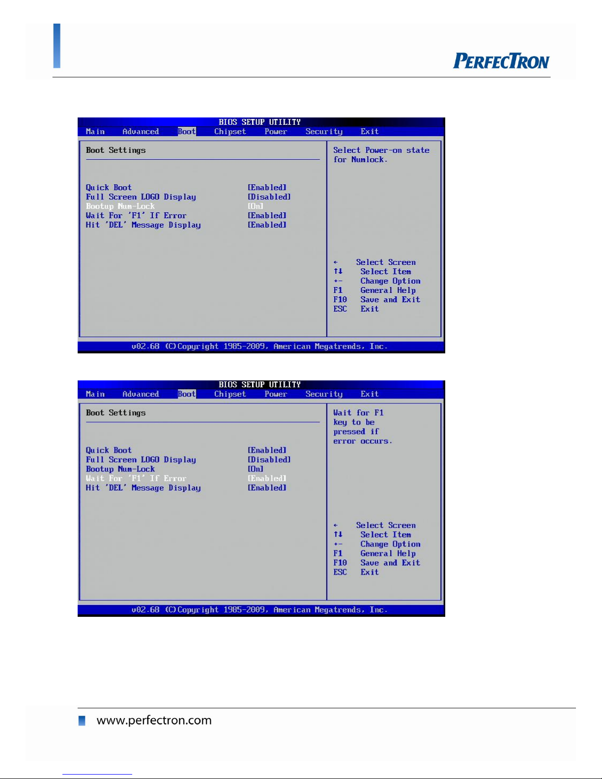
Bootup Num-lock
Wait For ‘F1’ If Error
Page 45
OXY5313A 3.5” SBC User’s Manual
45
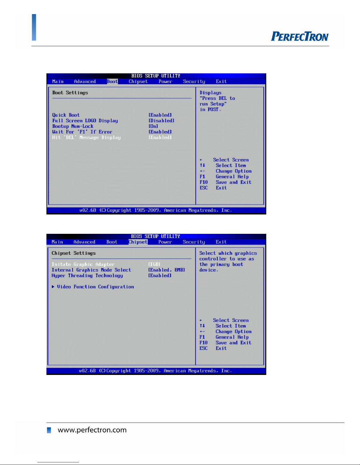
Hit ‘Del’ Message Display
4.6 Chipset Setting
Page 46
OXY5313A 3.5” SBC User’s Manual
46
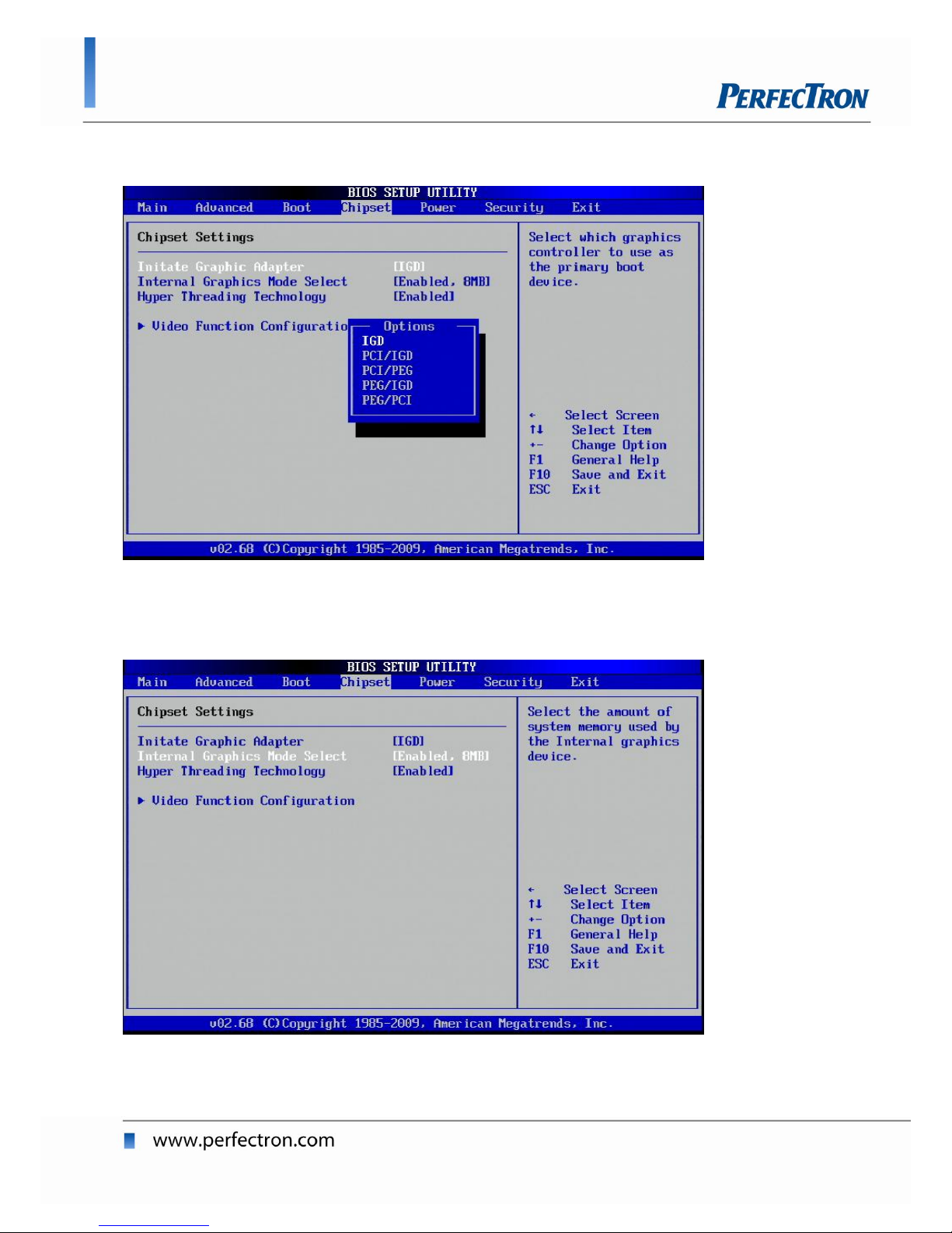
Initial Graphic Adapter
When this setting is selected, you should see options for IGD, PCI/IGD,
PEG/PCI, PCI/PEG and PEG/IGD.
IGD (Integrated Graphic Devices)
PEG (PCI express Graphic)
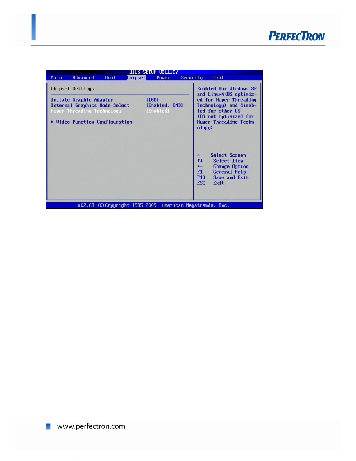
Internal Graphic Mode Select
Page 47
OXY5313A 3.5” SBC User’s Manual
47
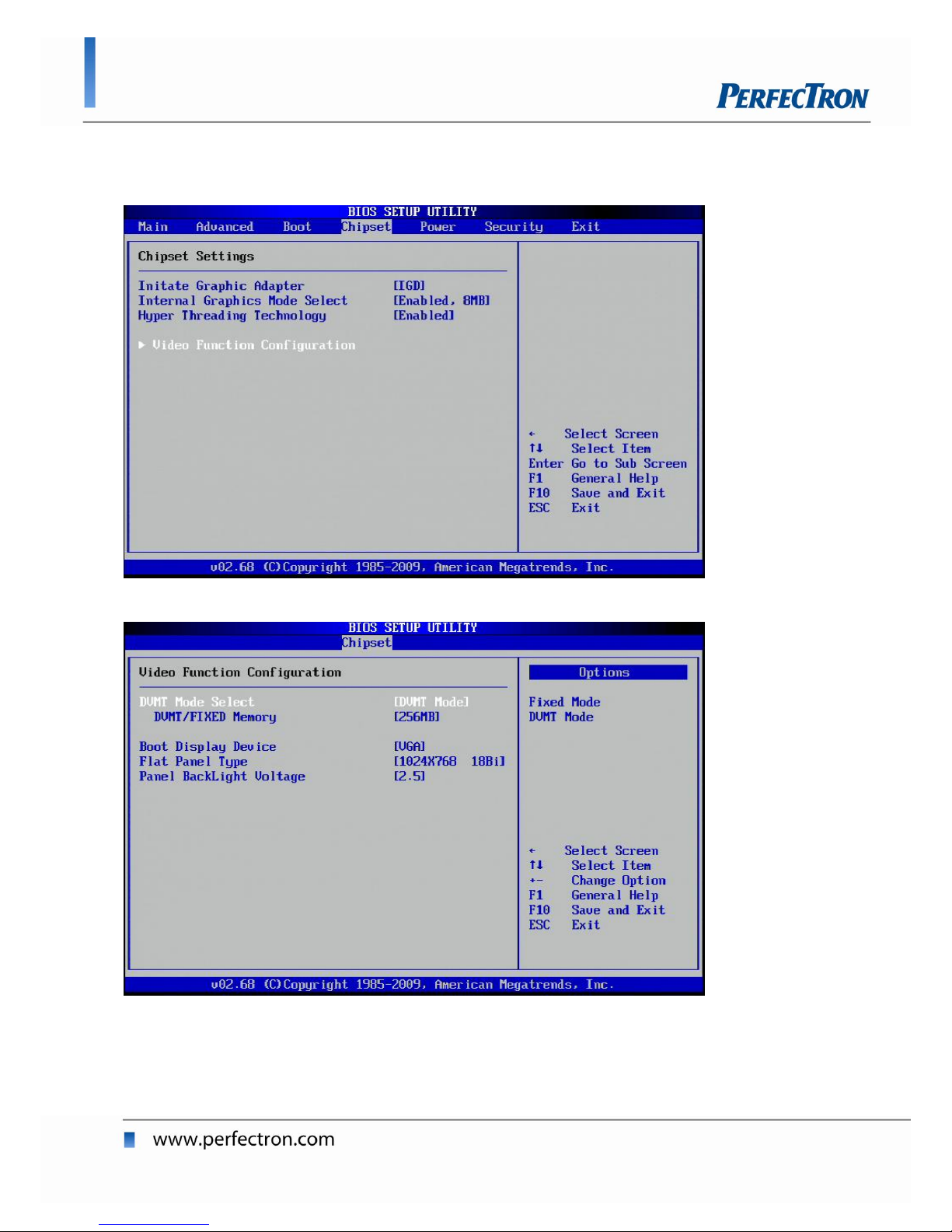
Hyper Threading Technology
Hyper-threading technology (HTT) is Intel's term for its simultaneous
multithreading implementation in some of its CPUs.
Hyper-threading is an Intel-proprietary technology used to improve
performance of multiple tasks running simultaneously. For each processor
core that is physically present, the operating system addresses two virtual
processors, and divides the workload. Hyper-threading requires system
support for multiple processors and HTT optimization. It is recommended
disabling HTT when using operating systems that have not been optimized
for this chip feature.
(The default BIOS setting is Enabled)
Page 48
OXY5313A 3.5” SBC User’s Manual
48
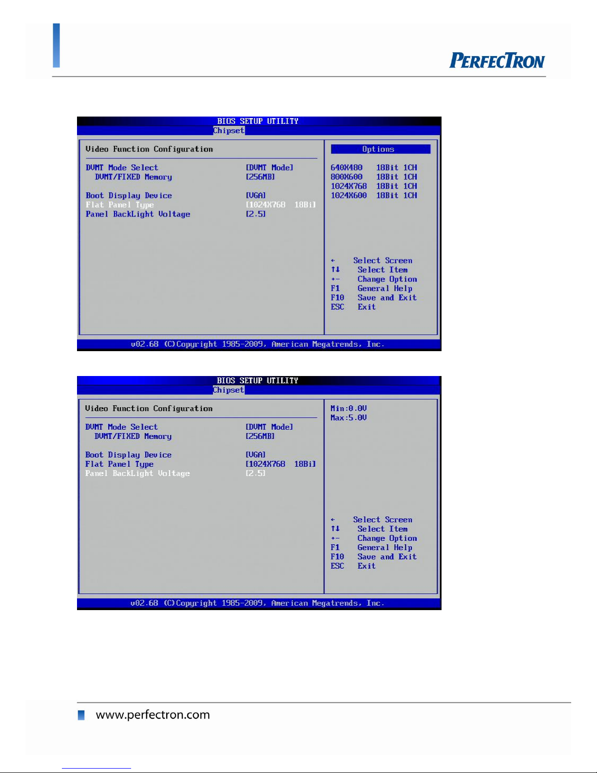
Video Function Configuration
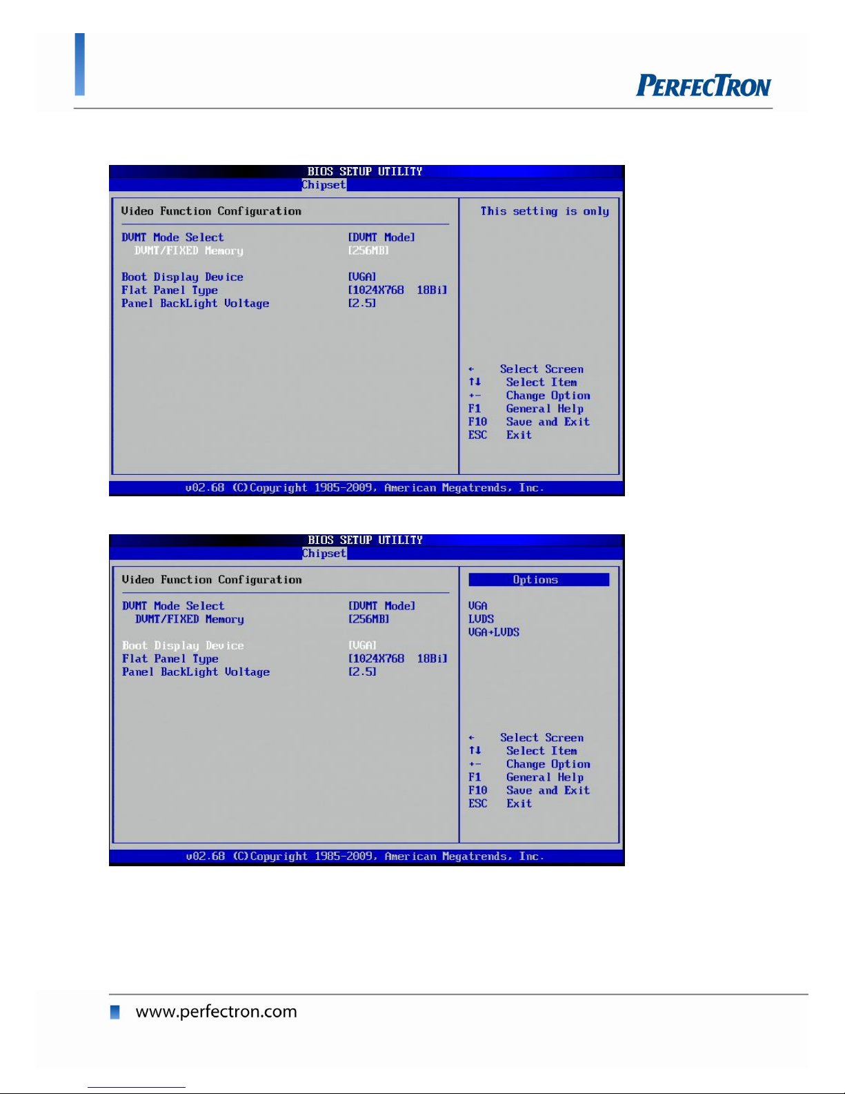
DVMT Model Select
DVMT Mode contains the following settings: Fixed Mode, DVMT Mode
Page 49
OXY5313A 3.5” SBC User’s Manual
49
DVMT/Fixed Memory
Boot Display Device
This setting allows you to setup VGA/LVDS/VGA+LVDS display mode.
Page 50
OXY5313A 3.5” SBC User’s Manual
50
Flat Panel Type
This setting allows you to setup the resolution for an onboard 18-bit LVDS.
Panel Backlight voltage
Setup the voltage for Panel
Page 51
OXY5313A 3.5” SBC User’s Manual
51
4.7 Power Management Setting
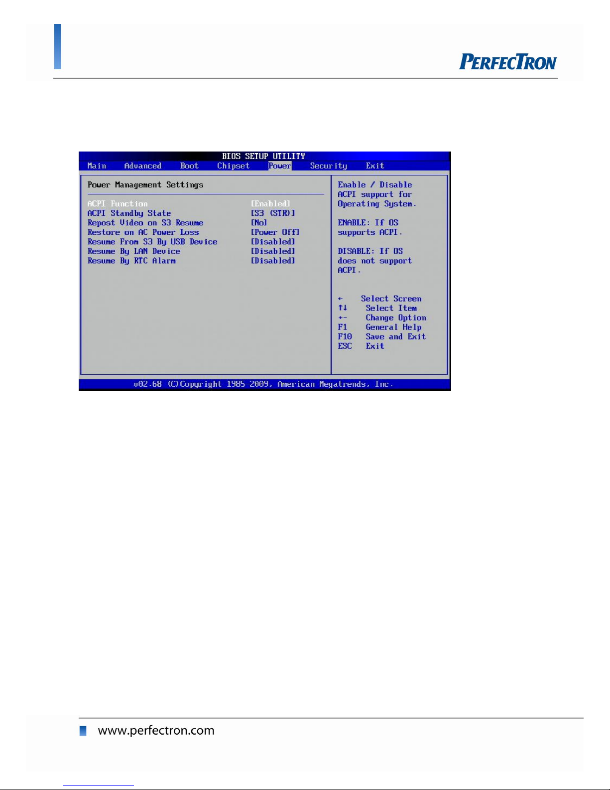
ACPI Function
This BIOS feature is used to enable or disable the motherboard's APCI
(Advanced Configuration and Power Interface)
Page 52
OXY5313A 3.5” SBC User’s Manual
52
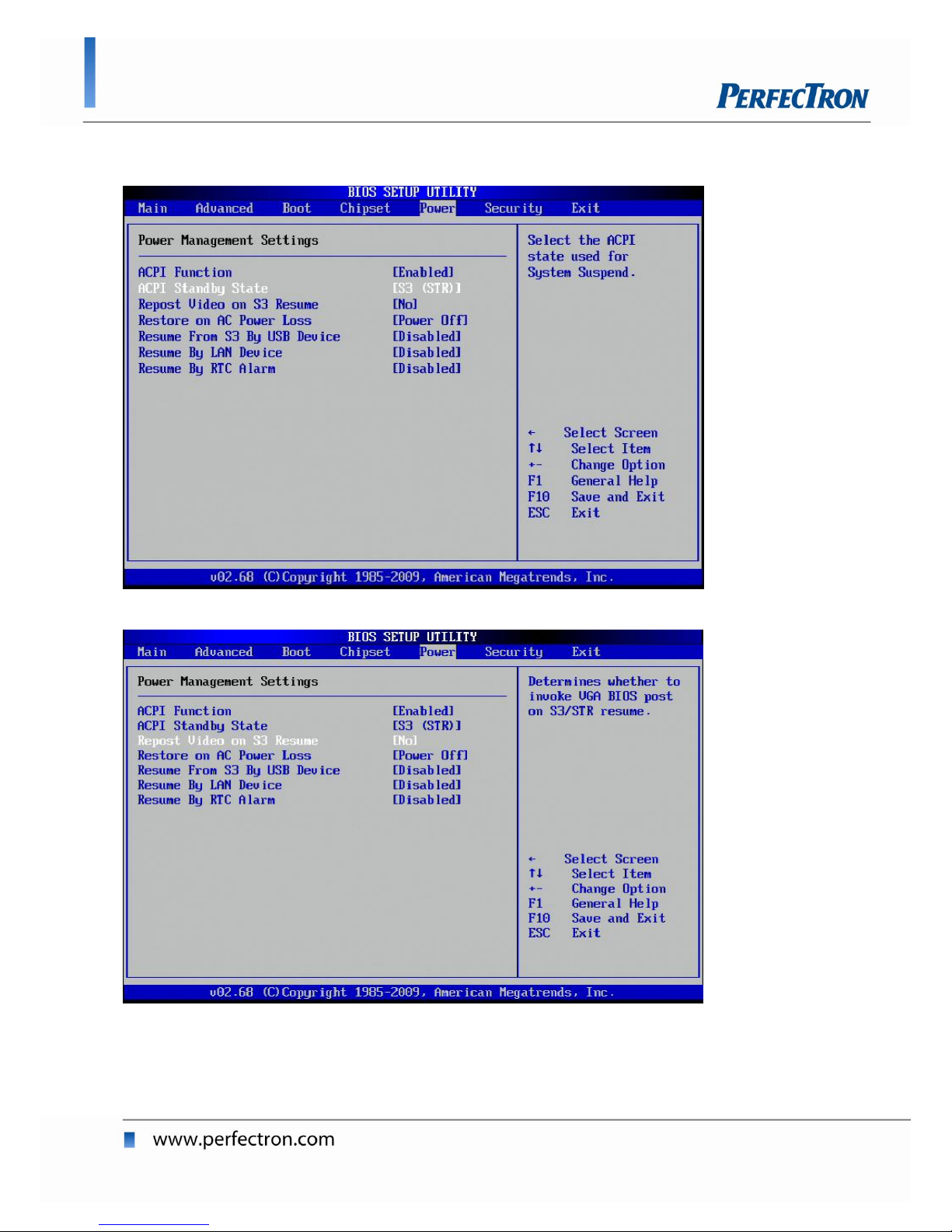
ACPI Standby State
Repost Video on S3 Resume
This setting controls the state of the system when it receives an ACPI
standby signal (OS Independent)
Page 53
OXY5313A 3.5” SBC User’s Manual
53
S3 = Suspend to RAM - The system powers off while maintaining the active
state of the system.
S1 = Power ON Standby - The system remains powered on but in a low
power state (CPU is idle but powered, usually fans and other modules are
still active - hard drives spin down).
The S3 setting is preferable, but some people still have to use the S1 setting
for various reasons. Either setting should not present problems to any
operating system.
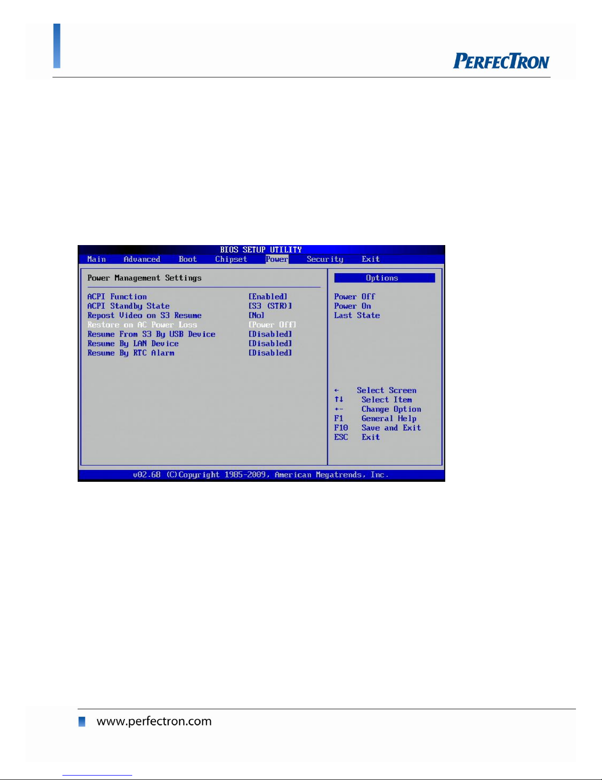
Restore on AC Power Loss
Restore the computer to power up when power is lost. You can set this by
entering the computers BIOS setup and configure this setting in the Power
Management Settings menu.
Page 54
OXY5313A 3.5” SBC User’s Manual
54
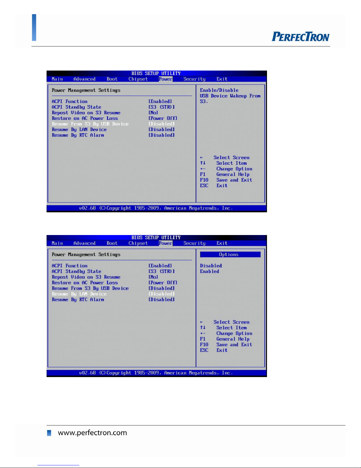
Resume From S3 By USB Device
Enable or disable this BIOS setting to wake up the computer by USB
Devices
Resume By LAN Device
Enable or disable this BIOS setting to wake up the computer by LAN1/LAN2
Port
Page 55
OXY5313A 3.5” SBC User’s Manual
55
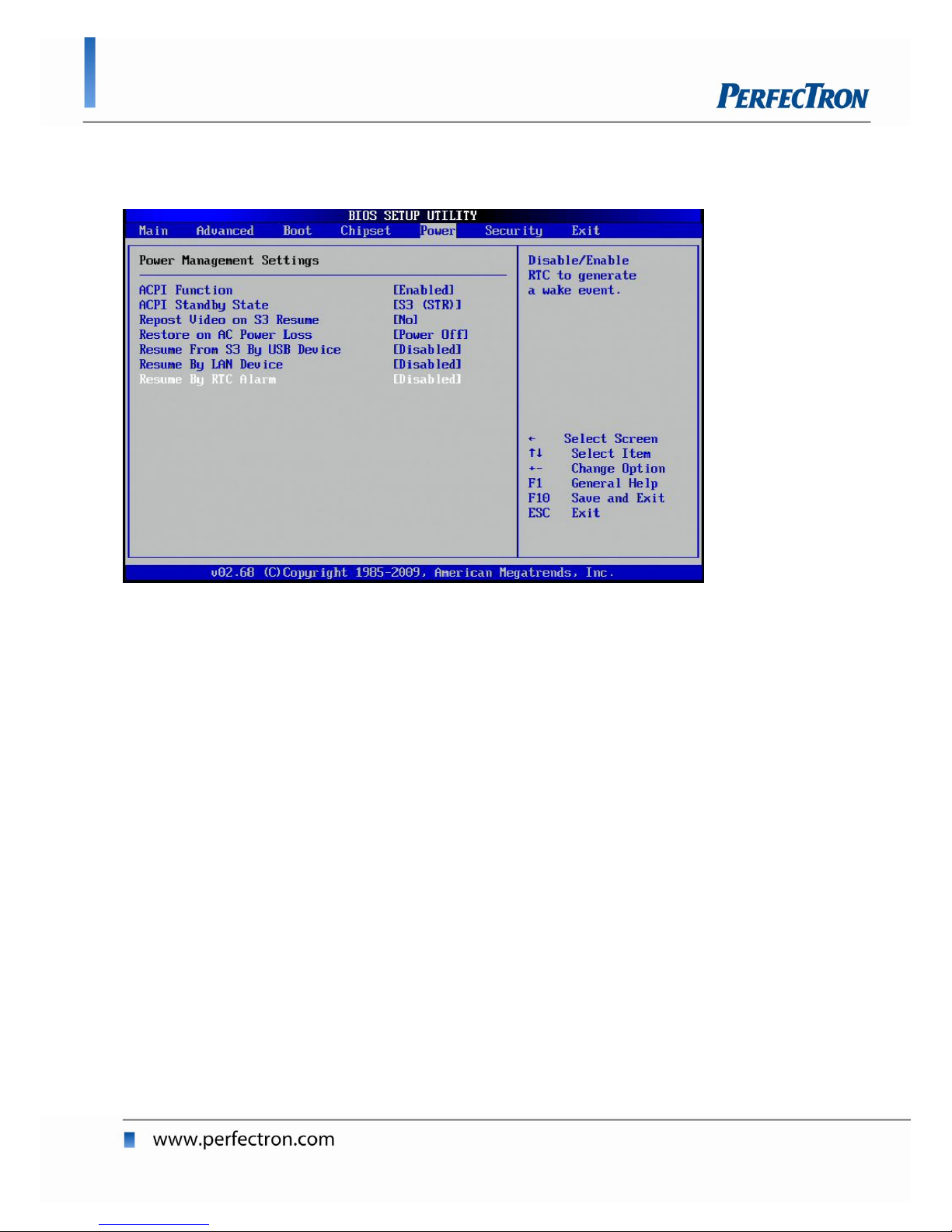
Resume By RTC Alarm
Enable or disable this BIOS setting to wake up the computer by RTC Alarm
4.8 Security Setting
Select this option to set the Security parameters. Select an option to
configure. The following settings are available:
Change Supervisor Password: Select to set the supervisor password.
Change User Password: Select to set the user password.
Page 56
OXY5313A 3.5” SBC User’s Manual
56
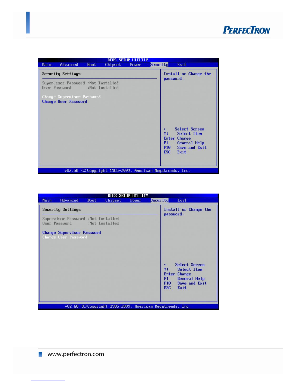
Change Supervisor Password
Select this option to set the Supervisor Password parameters.
Change User Password
Page 57
OXY5313A 3.5” SBC User’s Manual
57
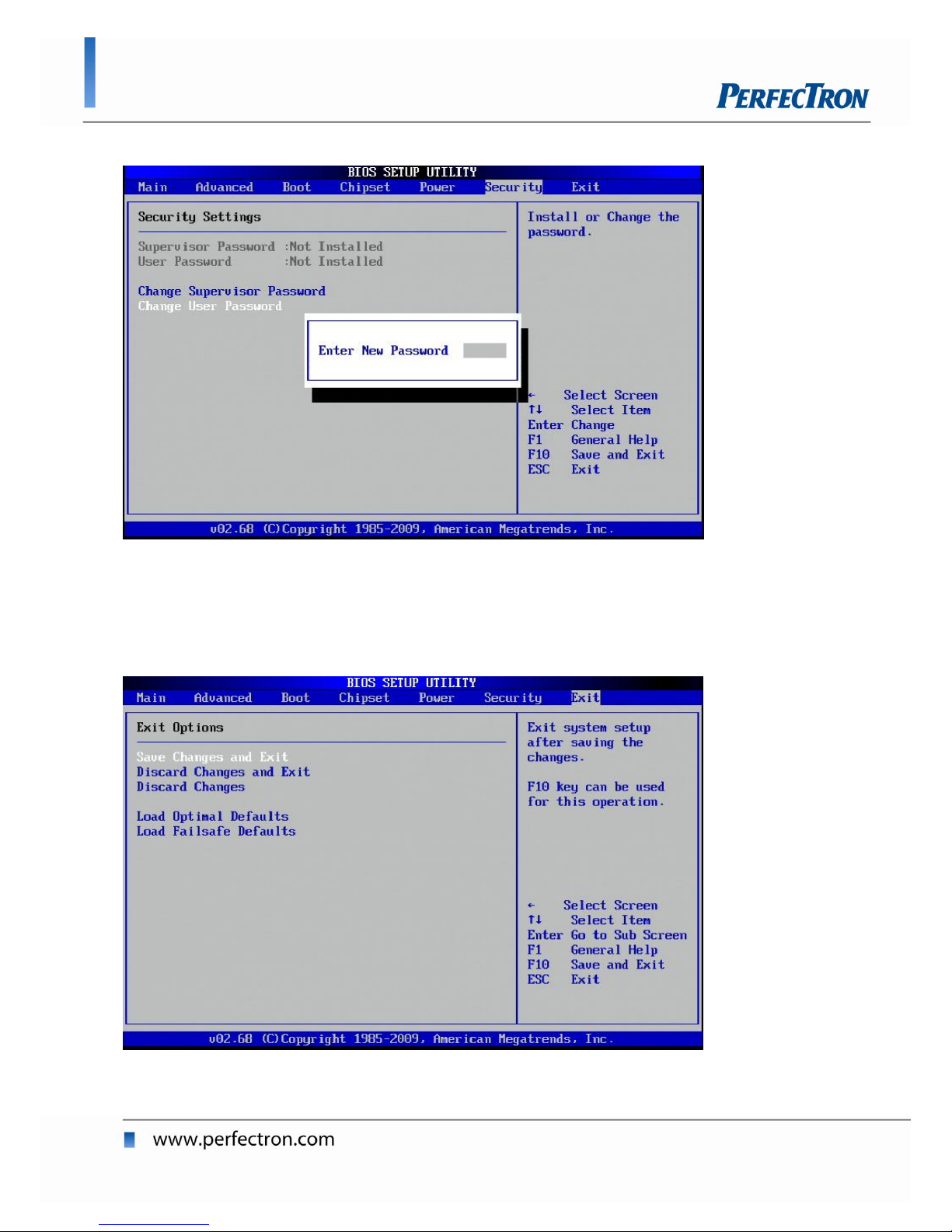
Select this option to set the User Password parameters.
4.9 Exit Setting
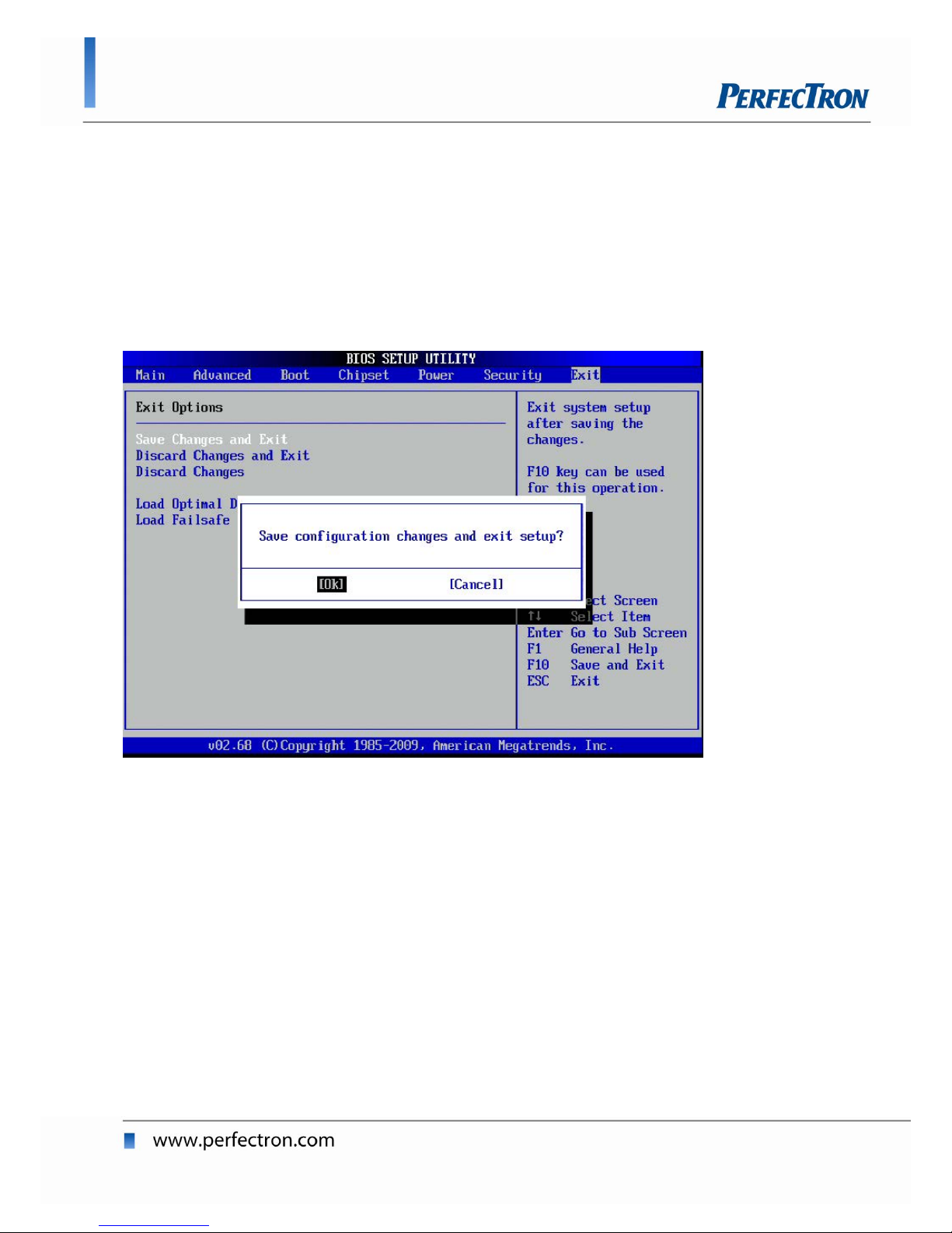
Save Changes and Exit
Page 58
OXY5313A 3.5” SBC User’s Manual
58
Select this menu to set the Exit parameters. The following settings are
available:
Save Changes and Exit: Select to set this parameter.
Discard Changes and Exit: Select to set this parameter.
Discard Changes: Select to set this parameter.
Load Optimal Defaults: Select to set this parameter.
Load Failsafe Defaults: Select to set this parameter.
Select this option to save any changes applied and exit the system.
Page 59
OXY5313A 3.5” SBC User’s Manual
59
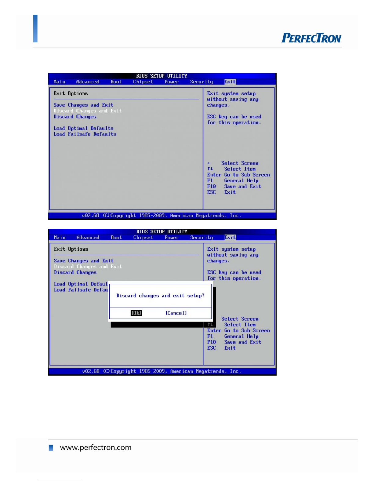
Discard Changes and Exit
Select this option to discard any changes applied and exit the system.
Page 60
OXY5313A 3.5” SBC User’s Manual
60
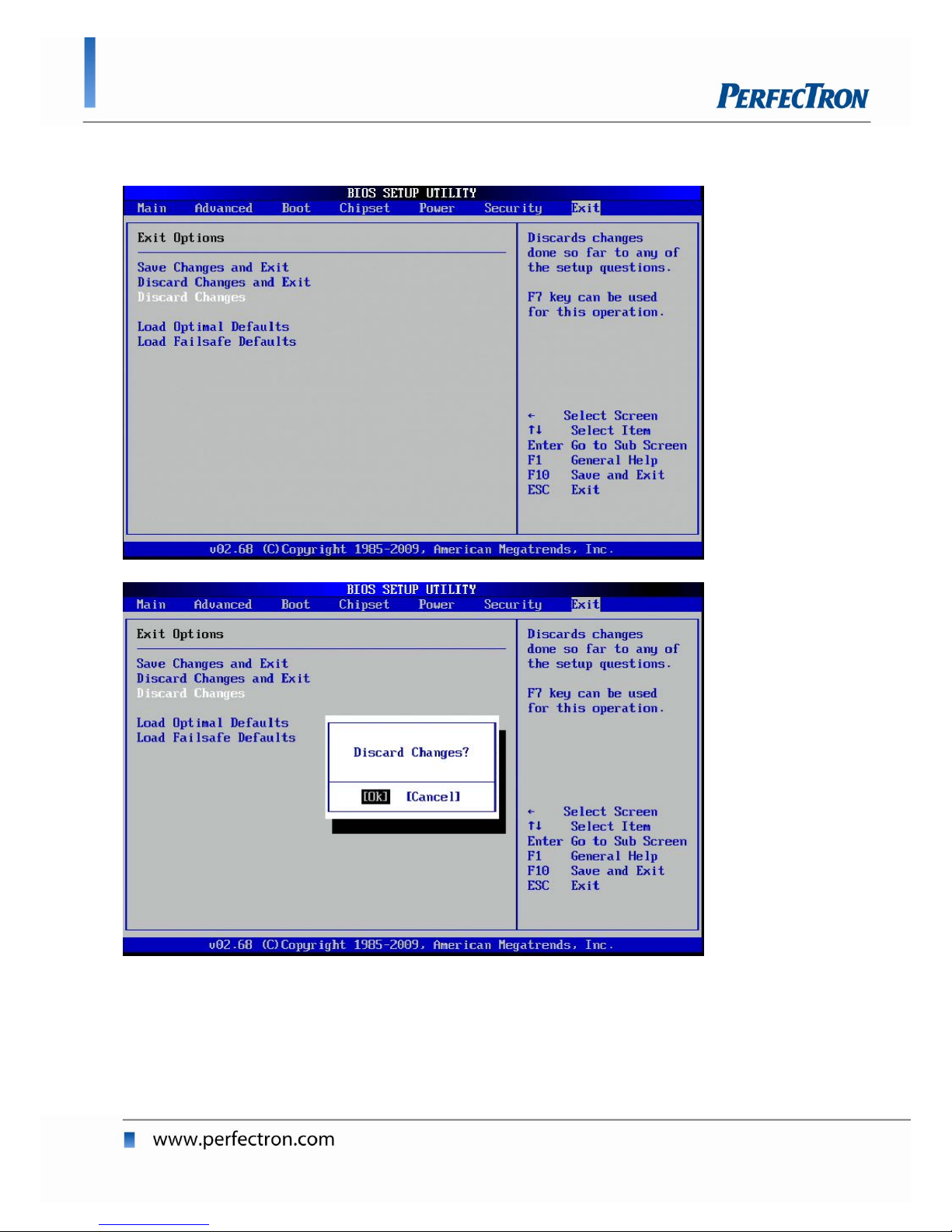
Discard Changes
Select this option to discard any changes applied.
Page 61
OXY5313A 3.5” SBC User’s Manual
61
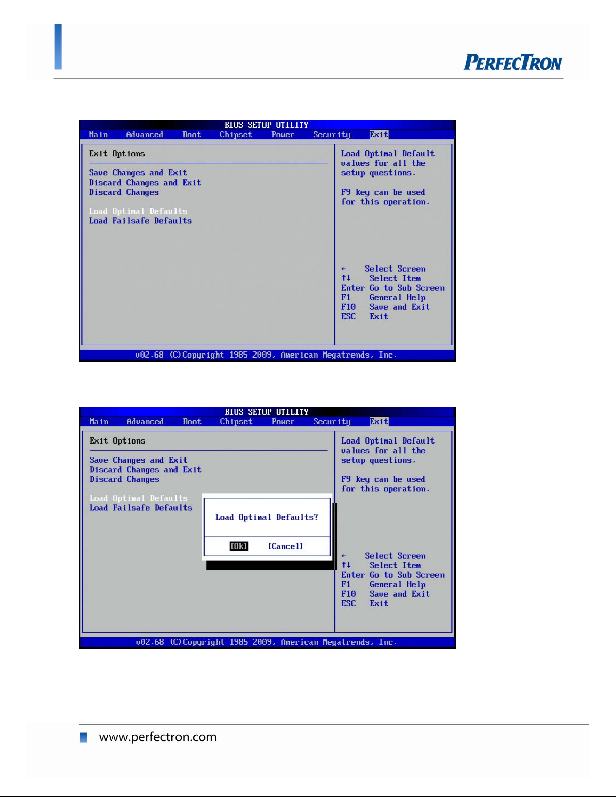
Load Optimal Defaults
Select this option to load optimal defaults.
Page 62
OXY5313A 3.5” SBC User’s Manual
62
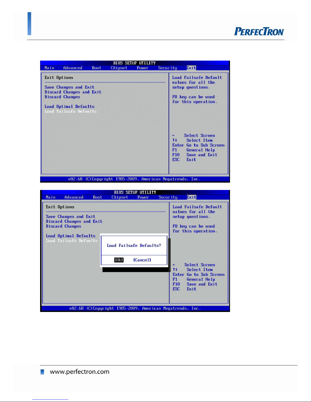
Load Failsafe Defaults
Select this option to load failsafe defaults.
Page 63

OXY5313A 3.5” SBC User’s Manual
63
APPENDIX A Watchdog Timer Setting
After the system stops working for a while, it can be auto-reset by the
Watchdog Timer. The integrated Watchdog Timer can be set up in the
system reset mode by program.
Using the Watchdog Function
Start
↓
Un-Lock WDT
↓
Set WDT Function
Select Logic device
↓
Activate WDT
:O 2E 87 ; Un-lock super I/O
O 2E 87 ; Un-lock super I/O
O 2E 2D O 2F 20
O 2E 07
O 2F 08
:O 2E 30
O 2F 01
Set Second or Minute
↓
Set base timer
↓
WDT counting
O 2E F5
O 2F N N=00 or 08(See below
table)
:O 2E F6
O 2F M=00,01,02,…FF(Hex) ,Value=0
to 255
Page 64

OXY5313A 3.5” SBC User’s Manual
64
re-set timer :O 2E F6
O 2F M ; M=00,01,02,…FF(See below table)
↓
IF No re-set timer :WDT time-out, generate RESET
IF to disable WDT :O 2E 30
O 2F 00 ; Can be disable at any time
N=00
M= 00h: Time-out Disable
01h: Time-out occurs after 1 second
02h: Time-out occurs after 2 second
03h: Time-out occurs after 3 second
……………………….......................................
FFh: Time-out occurs after 255 second
N=08
M= 00h: Time-out Disable
01h: Time-out occurs after 1 minute
02h: Time-out occurs after 2 minutes
03h: Time-out occurs after 3 minutes
……………………….......................................
FFh: Time-out occurs after 255 minutes
Page 65
OXY5313A 3.5” SBC User’s Manual
65
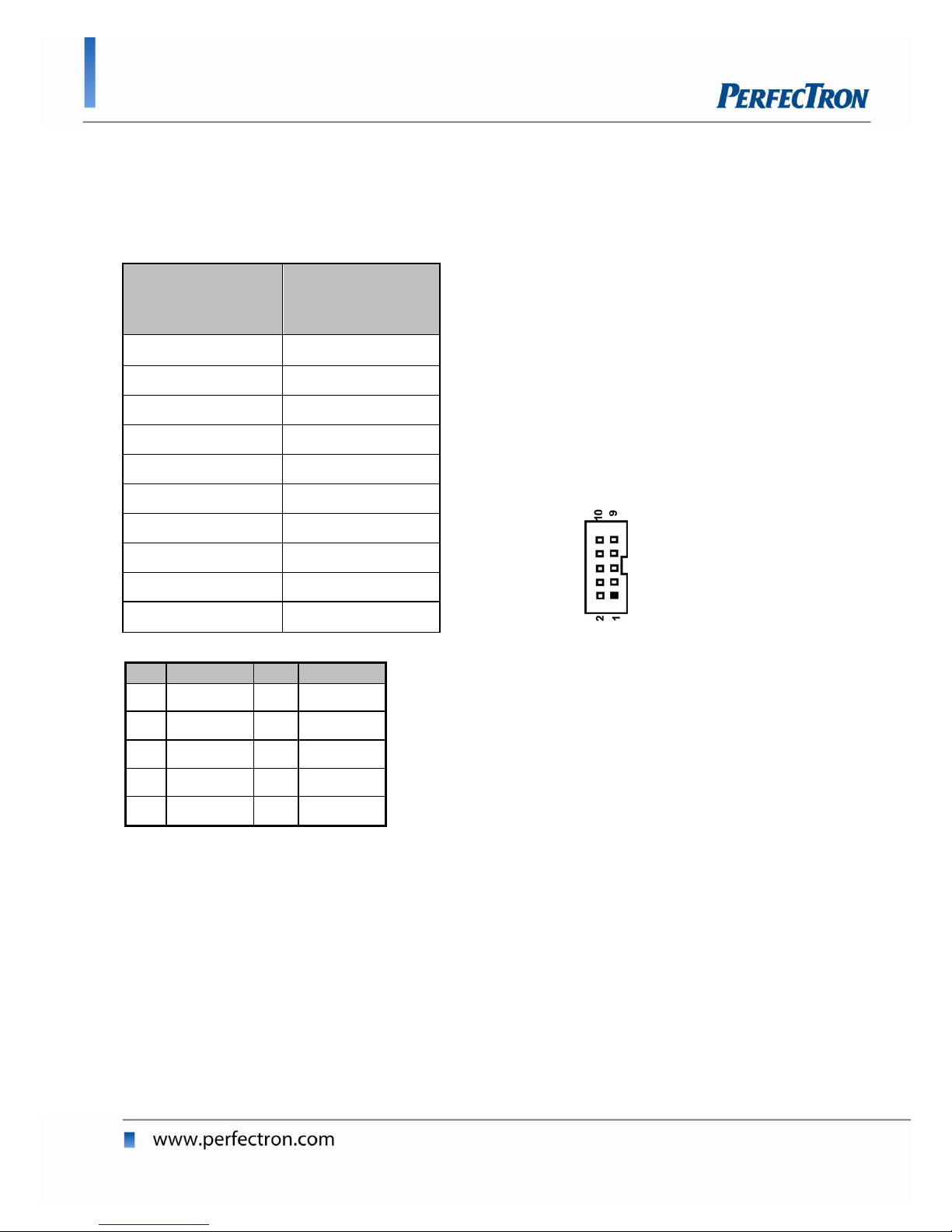
Pin Signal
Pin Signal
1
DI1 2 DO1
3
DI2 4 DO2
5
DI3 6 DO3
7
DI4 8 DO4
9
GND
10
GND
APPENDIX B DIGITAL I/O
Digital I/O Software Programming
Program Example: 4IN/4OUT (W83627DHG)
GPI
GPO
O 2E 87
O 2E 87
O 2E 87
O 2E 87
O 2E 07
O 2E 07
O 2F 09
O 2F 09
O 2E 30
O 2E 30
O 2F 02
O 2F F2
O 2E F0
O 2E F0
O 2F F0
O 2F F0
O 2E F1
O 2E F1
I 2F
O 2F M(Note)
Page 66

OXY5313A 3.5” SBC User’s Manual
66
Note:
Digital Output
Digital Input
Bit7
Bit6
Bit5
Bit4
Bit3
Bit2
Bit1
Bit0
DI4
DI3
DI2
DI1
DO4
DO3
DO2
DO1
 Loading...