

Motherboard
User Manual
MLB 2203/2213
Sep. 2006 (Revision B)
P/N: 1230B0026701

CCooppyyrriigghhtt NNoottiiccee
All rights, including copyright, in the content of this manual are owned or controlled by IESC and
protected by the Taiwan and international copyright act.
No one may, transmit, adapt, assign, compile, rent, sale, change, copy, reproduce, distribute, publish,
display, broadcast, or use in any way the content of this manual, in whole or in part, for any other
purpose whatsoever without the prior written permission of IESC.
TTrraaddeemmaarrkkss
All product names or brands mentioned herein are the trademarks of IESC, its subsidiaries or other
respective owners in Taiwan, United States and other countries.
DDiissccllaaiimmeerr
This manual provides the information in relation to the set-up and installation of the product herein.
Nothing herein may be construed as granting any right or license relating to any intellectual property
rights of this manual or product. Unless otherwise provided in the Purchase and Sale Agreement for
this product, manufacturer and distributor of this product will not be liable whatsoever relating to the
distribution and/or use of this product. In addition, manufacturer and distributor of this product hereby
specifically disclaim any express or implied warranties of merchantability, fitness for a particular
purpose, or non-infringement of third party rights in connection with this product.
Manufacturer of this product may have the right to change specifications and product descriptions at
any time without notice.

CCoonntteennttss
About This Manual ........................................................................................................................................i
Conventions..................................................................................................................................................i
Safety Symbols............................................................................................................................................ii
Safety Precautions......................................................................................................................................iii
Operation Safety.....................................................................................................................................iii
Electrical Safety.....................................................................................................................................iii
Battery Replacement Safety...................................................................................................................iv
Laser Peripherals or Devices Safety........................................................................................................v
Intended Application Uses.......................................................................................................................v
Site Selection...........................................................................................................................................v
Tools Required ........................................................................................................................................v
Regulatory and Integration Information.....................................................................................................vi
Regulatory Compliance Identification Numbers....................................................................................vi
Product Regulatory Compliance ............................................................................................................vi
1 Introduction........................................................................................................................................1-1
1.1 Audience Assumptions.................................................................................................................1-1
1.2 Manual Organization....................................................................................................................1-1
1.3 Product Features...........................................................................................................................1-2
1.4 Motherboard Layout.....................................................................................................................1-4
1.4.1 Connectors and Component Locations.................................................................................1-4
1.4.2 Back Panel Connectors.........................................................................................................1-6
1.4.3 System LED Information .....................................................................................................1-6
1.4.4 Port 80 LEDs Information....................................................................................................1-7
2 Hardware Operations........................................................................................................................2-1
2.1 Before You Start ...........................................................................................................................2-1
2.2 Screw Holes..................................................................................................................................2-2
2.3 Battery..........................................................................................................................................2-3
2.3.1 To remove the battery...........................................................................................................2-4
2.3.2 To install the battery.............................................................................................................2-4
2.4 Processor ......................................................................................................................................2-5
2.4.1 To remove the heat sink........................................................................................................2-6
2.4.2 To install the heat sink..........................................................................................................2-6
2.4.3 To remove the processor.......................................................................................................2-7
2.4.4 To install the processor.........................................................................................................2-8
2.4.5 To remove the heat sink socket ............................................................................................2-9
2.4.6 To install the heat sink socket...............................................................................................2-9
2.5 System Memory ......................................................................................................................... 2-10
2.5.1 DIMM Population..............................................................................................................2-10
2.5.2 To remove a DIMM............................................................................................................2-13

2.5.3 To install a DIMM..............................................................................................................2-14
2.6 System Configuration Jumper....................................................................................................2-15
3 Connectors and Jumper.....................................................................................................................3-1
3.1 Power Connectors (J8, J6)............................................................................................................3-1
3.1.1 Main Power Connector (J8) .................................................................................................3-1
3.1.2 Processor Power Connector (J6) ..........................................................................................3-2
3.2 Front Panel IDE Connector (J24).................................................................................................3-3
3.3 Floppy Connector (J45)................................................................................................................3-5
3.4 Chassis Intrusion Connector (J27)................................................................................................3-6
3.5 Front Panel VGA Connector (J68)...............................................................................................3-7
3.6 D-sub VGA Port (J61)..................................................................................................................3-8
3.7 Serial Port (J62)............................................................................................................................3-9
3.8 Keyboard and Mouse Ports (J60, J59)........................................................................................3-10
3.9 Rear Dual USB Port (J58)..........................................................................................................3-12
3.10 Front Panel USB Connector (J19)..............................................................................................3-13
3.11 I
2
C (SMBus) Signal Connector for PSU (J20)...........................................................................3-14
3.12 Two Dual NIC Connectors (RJ45) (J56, J57).............................................................................3-15
3.13 Management Port (RJ45) (J75) ..................................................................................................3-17
3.14 Fan Board Connector (J1) ..........................................................................................................3-18
3.15 Mini-SAS Connectors (J69, J70, J71, J72).................................................................................3-19
3.16 LCM Connector (Optional) (J73)...............................................................................................3-20
3.17 Internal USB Port for USB Floppy (J67)...................................................................................3-21
3.18 System Configuration Jumper Setting (J54)...............................................................................3-22
4 BIOS Setup .........................................................................................................................................4-1
4.1 BIOS Setup Utility.......................................................................................................................4-1
4.2 Entering the BIOS Setup Utility...................................................................................................4-2
4.3 Keyboard Command Bar..............................................................................................................4-3
4.4 BIOS Updates...............................................................................................................................4-5
4.4.1 BIOS Requirements..............................................................................................................4-5
4.4.2 ROM Flash ...........................................................................................................................4-5
LLiisstt ooff FFiigguurreess
Figure 1-1 Motherboard Overview....................................................................................................1-2
Figure 1-2 Connectors and Component Locations............................................................................1-4
Figure 1-3 Back Panel Connectors....................................................................................................1-6
Figure 1-4 Port 80 LEDs...................................................................................................................1-7
Figure 2-1 Screws Placement............................................................................................................2-2
Figure 2-2 Battery Location..............................................................................................................2-3
Figure 2-3 Pulling the Battery out of the Holder...............................................................................2-4
Figure 2-4 Putting the Battery into the Holder..................................................................................2-4
Figure 2-5 Processor Location ..........................................................................................................2-5
Figure 2-6 Pulling up the Heat Sink..................................................................................................2-6

Figure 2-7 Opening the Load Plate ...................................................................................................2-7
Figure 2-8 Lifting the Processor out of the Socket............................................................................2-7
Figure 2-9 Closing the Load Plate..................................................................................................... 2-7
Figure 2-10 Placing on the PnP Cap..................................................................................................2-8
Figure 2-11 Aiming the Golden Corner at the Socket.......................................................................2-8
Figure 2-12 Removing the Heat Sink Base Socket ...........................................................................2-9
Figure 2-13 Lifting up the Heat Sink Socket.....................................................................................2-9
Figure 2-14 System Memory Location............................................................................................2-10
Figure 2-15 Lifting the DIMM out of the Socket............................................................................2-13
Figure 2-16 Pressing the Retaining Clips Outward.........................................................................2-14
Figure 2-17 Inserting the DIMM into the Socket............................................................................2-14
Figure 2-18 System Configuration Jumper Location......................................................................2-15
Figure 3-1 Main Power Connector.................................................................................................... 3-1
Figure 3-2 Processor Power Connector.............................................................................................3-2
Figure 3-3 Front Panel IDE Connector .............................................................................................3-3
Figure 3-4 Floppy Connector............................................................................................................3-5
Figure 3-5 Chassis Intrusion Connector............................................................................................3-6
Figure 3-6 Front Panel VGA Connector............................................................................................3-7
Figure 3-7 D-sub VGA Port..............................................................................................................3-8
Figure 3-8 Serial Port........................................................................................................................3-9
Figure 3-9 Keyboard Port................................................................................................................3-10
Figure 3-10 Mouse Port...................................................................................................................3-11
Figure 3-11 Rear Dual USB Port.....................................................................................................3-12
Figure 3-12 Front Panel USB Connector ........................................................................................ 3-13
Figure 3-13 I
2
C (SMBus) Signal Connector for PSU......................................................................3-14
Figure 3-14 Dual NIC Connector (RJ45)........................................................................................3-15
Figure 3-15 Management Port (RJ45).............................................................................................3-17
Figure 3-16 Fan Board Connector...................................................................................................3-18
Figure 3-17 Mini-SAS Connector...................................................................................................3-19
Figure 3-18 LCM Connector...........................................................................................................3-20
Figure 3-19 Internal USB Port for USB Floppy..............................................................................3-21
Figure 3-20 System Configuration Jumper .....................................................................................3-22
LLiisstt ooff TTaabblleess
T able 1-1 Introduction of the Manual................................................................................................1-1
T able 1-2 Product Features................................................................................................................1-2
T able 1-3 LED Information...............................................................................................................1-6
T able 1-4 Code Information..............................................................................................................1-8
T able 1-5 Boot Block Initialization Code Checkpoints.....................................................................1-8
T able 1-6 Bootblock Recovery Code Checkpoints............................................................................1-9
Table 1-7 POST Code Information..................................................................................................1-10
Table 1-8 DIM Code Checkpoints...................................................................................................1-13
T able 1-9 ACPI Runtime Checkpoints............................................................................................1-13
T able 1-10 Beep Codes....................................................................................................................1-13

T able 1-11 Troubleshooting BIOS Beep Codes...............................................................................1-14
T able 2-1 DIMM Installation Option 1 ...........................................................................................2-11
T able 2-2 DIMM Installation Option 2 ...........................................................................................2-12
Table 3-1 Main Power Connector Pin Definition..............................................................................3-2
Table 3-2 Processor Power Connector Pin Definition.......................................................................3-2
Table 3-3 Front Panel IDE Connector Pin Definition .......................................................................3-3
T able 3-4 Floppy Connector Pin Definition......................................................................................3-5
T able 3-5 Chassis Intrusion Connector Pin Definition......................................................................3-6
Table 3-6 Front Panel VGA Connector Pin Definition......................................................................3-7
T able 3-7 D-sub VGA Port Pin Definition........................................................................................3-8
Table 3-8 Serial Port Pin Definition ..................................................................................................3-9
T able 3-9 Keyboard Port Pin Definition..........................................................................................3-10
T able 3-10 Mouse Port Pin Definition.............................................................................................3-11
Table 3-11 Rear Dual USB Port Pin Definition...............................................................................3-12
Table 3-12 Front Panel USB Connector Pin Definition ..................................................................3-13
Table 3-13 I
2
C (SMBus) Signal Connector for PSU Pin Definition ...............................................3-14
Table 3-14 Dual NIC Connector (RJ45) Pin Definition ..................................................................3-15
T able 3-15 Management Port (RJ45) Pin Definition.......................................................................3-17
Table 3-16 Fan Board Connector Pin Definition.............................................................................3-18
Table 3-17 Mini-SAS Connector Pin Definition.............................................................................3-19
T able 3-18 LCM Connector Pin Definition.....................................................................................3-20
Table 3-19 Internal USB Port for USB Floppy Pin Definition........................................................3-21
Table 3-20 System Configuration Jumper Function........................................................................3-22
Table 4-1 BIOS Setup Utility Screen Description.............................................................................4-2
T able 4-2 Keyboard Command Bar Description...............................................................................4-3
Table 4-3 BIOS Requirements Description.......................................................................................4-5

About This Manual
About This Manual
Conventions
Safety Precautions
Regulatory and Integration Information

About This Manual
1230B0026701
i
AAbboouutt TThhiiss MMaannuuaall
CCoonnvveennttiioonnss
To make sure that you perform certain tasks properly, take note of the following symbols used
throughout this manual.
Warning:
Information to prevent injury to yourself when trying to complete a task.
Caution:
Information to prevent damage to the components when trying to complete
a task.
Important:
Information that you must follow to complete a task.
Note:
Tips and information to aid in completing a task.
About This Manual
1230B0026701
ii
SSaaffeettyy SSyymmbboollss
Before troubleshooting, you must be familiar with the safety information listed below. In order to avoid
any potential hazards, the following symbols may be placed on some components of the server.
The shape and the color of symbols shown below are mainly for your reference. Please take the actual
shipment as standard.
Indicates the potential hazard of energy circuits or electric shock. To reduce the risk of
injury from electric hazards, do not open this enclosure.
Warning: Any surface or area of the equipment marked with this symbol indicates the
presence of electric shock hazards. The enclosed area contains no operator serviceable
parts.
Indicates the potential hazard of electric shock. The enclosed area contains no user of
field serviceable parts. Do not open for any reason.
Warning: To reduce the risk of injury from electric shock hazards, do not open this
enclosure.
Indicates the presence of a hot surface or hot component.
Warning: To reduce the risk of injury from a hot component, allow the surface to co
o
before touching it.
Any RJ45 receptacle marked with this symbol indicates a network interface connection
.
Warning: To reduce the risk of electric shock, fire, or damage to the equipment, do no
t
plug telephone or telecommunications connectors into this receptacle.
This symbol, on power supplies or systems, indicates that the equipment is supplied
by multiple sources of power.
Warning: To reduce the risk of injury from electric shock, remove all power cords to
completely disconnect power from the system.
Weight in kg
Weight in lb
This symbol indicates that the component exceeds the recommended weight for one
individual to handle safely.
Warning: To reduce the risk of personal injury or damage to the equipment, observe
local occupational health and safety requirements and guidelines for manual material
handling.

About This Manual
1230B0026701
iii
SSaaffeettyy PPrreeccaauuttiioonnss
Observe the following safety precautions when you are connecting or disconnecting any device.
Regarding the standards of workstation regulations, do not place the server in the visual
field of the user, because of the glossy front of the case.
The product is non-consumer product and for profession technical person used only.
Operation Safety
Any operation on this server must be conducted by certified or experienced engineers.
Before operating your server, carefully read all the manuals included with the server package.
Before using the server, make sure that all cables are correctly connected and power cables are not
damaged. If any damage is detected, contact your dealer as soon as possible.
To avoid short circuits, keep paper clips, screws, and staples away from connectors, slots, sockets
and circuitry.
Before opening the chassis panels, make sure all power cables are unplugged.
Avoid dust, humidity, and extreme temperatures, place the server on a stable surface.
If the power supply is broken, do not try to fix it by yourself. Contact an authorized dealer.
It is recommended that you wear gloves when assembling or dissembling the server to protect
from cuts and scrapes.
When the server is powered on, heat sinks and the surfaces of certain IC devices may be hot. Do
not touch them. Check whether the fans are functioning properly.
Electrical Safety
Before installing or removing signal cables, ensure that the power cables for the system unit and
all attached devices are unplugged.
To prevent electric shock hazard, disconnect the power cable from the electrical outlet before
relocating the system.
When adding or removing any additional devices to or from the system, ensure that the power
cables for those devices are unplugged before the signal cables are connected. If possible,
disconnect all power cables from the existing system before you add a device.
Use one hand, when possible, to connect or disconnect signal cables to prevent a possible shock
from touching two surfaces with different electrical potentials.

About This Manual
1230B0026701
iv
This product is equipped with a three-wire power cable and plug for user safety. Use the power
cable with a properly grounded electrical outlet to avoid electric shock.
Motherboards, adapters, and disk drives are sensitive to static electricity discharge. These devices are
wrapped in antistatic bags to prevent this damage. Take the following precautions:
If you have an antistatic wrist strap available, use it while handling the device.
Do not remove the device from the antistatic bag until you are ready to install the device in the
system unit.
With the device still in its antistatic bag, touch it to a metal frame of the system.
Grasp cards and boards by the edges. Hold drives by the frame. Avoid touching the solder joints
or pins.
If you need to lay the device down while it is out of the antistatic bag. Lay it on the antistatic bag.
Before picking it up again, touch the antistatic bag and the metal frame of the system unit at the
same time.
Handle the devices carefully to prevent permanent damage.
Battery Replacement Safety
This server is provided with an internal Lithium battery or battery pack. There is a danger of explosion
and risk of personal injury if the battery is incorrectly replaced or mistreated.
For more information about battery replacement or proper disposal, contact an authorized reseller or your
authorized service provider.
This server contains an internal Lithium Manganese Dioxide, or a Vanadium Pentoxide, or an
alkaline battery pack. There is risk of fire and burns if the battery pack is not handled
properly. To reduce the risk of personal injury:
Do not attempt to recharge the battery.
Do not expose to temperatures higher than 70°C.
Do not disassemble, crush, puncture, shorten external contacts, or dispose in fire or water
.
Replace only with the spare parts designated for this product.
Batteries should not be littered along with the general household waste. Please use the public
collection system or return them to the supplier.

About This Manual
1230B0026701
v
Laser Peripherals or Devices Safety
To avoid risk of radiation exposure and/or personal injury:
Do not open the enclosure of any laser peripheral or device.
Laser peripherals or devices have are not user serviceable.
Return to manufacturer for servicing.
Intended Application Uses
This product was evaluated as Information Technology Equipment (ITE), which may be installed in
offices, schools, computer rooms, and similar commercial type locations. The suitability of this product
for other product categories and environments (such as medical, industrial, residential, alarm systems,
and test equipment), other than an ITE application, may require further evaluation.
Site Selection
The system is designed to operate in a typical office environment. Choose a site that is:
Clean, dry, and free of airborne particles (other than normal room dust).
Well-ventilated and away from sources of heat including direct sunlight and radiators.
Away from sources of vibration or physical shock.
Isolated from strong electromagnetic fields produced by electrical devices.
In regions that are susceptible to electrical storms, we recommend you plug your system into a
surge suppresser and disconnect telecommunication lines to your modem during an electrical
storm.
Provided with a properly grounded wall outlet.
Provided with sufficient space to access the power supply cord(s), because they serve as the
product's main power.
Tools Required
A cross screwdriver or a flat screwdriver is needed to install or remove the components in the server.

About This Manual
1230B0026701
vi
RReegguullaattoorryy aanndd IInntteeggrraattiioonn IInnffoorrmmaattiioonn
Regulatory Compliance Identification Numbers
For the purpose of regulatory compliance certifications and identification, this motherboard is assigned a
serial number. This server serial number can be found on the product label, along with the required
approval markings and information. When requesting certification information for this product, always
refer to this serial number. This serial number should not be confused with the marketing name or model
number.
Product Regulatory Compliance
Product Safety Compliance
The motherboard complies with the following safety requirements:
IEC 60950-1 Safety of Information Technology Equipment
EN 60950-1 Safety of Information Technology Equipment Including Electrical Business
Equipment, European Committee for Electrotechnical Standardization
(CENELEC)
UL 60950-1 Safety of Information Technology Equipment
UL 94 T ests for Flammability of Plastic Materials for Parts in Devices & Appliances
GB4943 Safety of Information Technology Equipment
Worldwide Safety approvals can be supplied according to the requirements from Marketing or Customer.
Product EMC Compliance
This product has been tested and verified to comply with the following electromagnetic compatibility
(EMC) regulations.
Communications Commission Notice
Part 15 of the Federal Communications Commission (FCC) Rules and Regulations has established Radio
Frequency (RF) emission limits to provide an interference-free radio frequency spectrum. Many
electronic devices, including computers, generate RF energy incidental to their intended function and are,
therefore, covered by these rules. These rules place computers and related peripheral devices into two
classes, A and B, depending upon their intended installation. Class A devices are those that may
reasonably be expected to be installed in a business or commercial environment. Class B devices are
those that may reasonably be expected to be installed in a residential environment (for example, personal
computers). The FCC requires devices in both classes to bear a label indicating the interference potential
of the device as well as additional operating instructions for the user.
The rating label on the device shows which class (A or B) the equipment falls into. Class A devices do

About This Manual
1230B0026701
vii
not have an FCC logo or FCC ID on the label. Class B devices have an FCC logo or FCC ID on the label.
Once the class of the device is determined, refer to the following corresponding statement.
Class A Equipment
This equipment has been tested and found to comply with the limits for a Class A digital device,
pursuant to Part 15 of the FCC Rules. These limits are designed to provide reasonable protection against
harmful interference when the equipment is operated in a commercial environment. This equipment
generates, uses, and can radiate radio frequency energy and, if not installed and used in accordance with
the instructions, may cause harmful interference to radio communications. Operation of this equipment
in a residential area is likely to cause harmful interference, in which case the user will be required to
correct the interference at personal expense.
Declaration of Conformity for Products Marked with the FCC Logo—United States Only
This device complies with Part 15 of the FCC Rules Operation and is subject to the following two
conditions: (1) this device may not cause harmful interference, and (2) this device must accept any
interference received, including interference that may cause undesired operation.
For questions regarding your product, please contact the supplier.
To identify this product, refer to the Part, Series, or Model number found on the product.
European Union Notice
Products with the CE Marking comply with both the EMC Directive (89/336/EEC) and the Low-Voltage
Directive (73/23/EEC) issued by the Commission of the European Community.
Compliance with these directives implies conformity to the following European Norms (in brackets are
the equivalent international standards):
EN55022 (CISPR 22) Electromagnetic Interference
EN55024 (IEC61000-4-2,3,4,5,6,8,11) Electromagnetic Immunity
EN61000-3-2 (IEC61000-3-2) Power Line Harmonics
EN61000-3-3 (IEC61000-3-3) Power Line Flicker
EN60950 (IEC950) Product Safety
About This Manual
1230B0026701
viii
Canadian Notice (Avis Canadien)
Class A Equipment
Japanese Notice
Taiwanese Notice

Chapter 1
Introduction
Audience Assumptions
Manual Organization
Product Features
Motherboard Layout

Introduction
1230B0026701
1-1
11 IInnttrroodduuccttiioonn
11..11 AAuuddiieennccee AAssssuummppttiioonnss
This manual assumes that you are a service technician or network administrator familiar with computer
hardware, data storage and network administration terminology and tasks.
11..22 MMaannuuaall OOrrggaanniizzaattiioonn
This manual introduces the motherboard and chassis along with the hardware information and how to
replace the hardware. This manual is generally organized as follows:
Table 1-1 Introduction of the Manual
Introduction
The general introduction to the server.
Hardware Operations
The operation of the components on the motherboard, such as battery,
processor, system memory, and so forth.
Connectors and Jumper
Some necessary information of the connectors and jumper on the
motherboard.
BIOS Setup
Information about BIOS setup.

Introduction
1230B0026701
1-2
11..33 PPrroodduucctt FFeeaattuurreess
This chapter provides the detailed features for processor, memory, onboard LAN, D-sub VGA, I/O and
PCI with pictures for your reference.
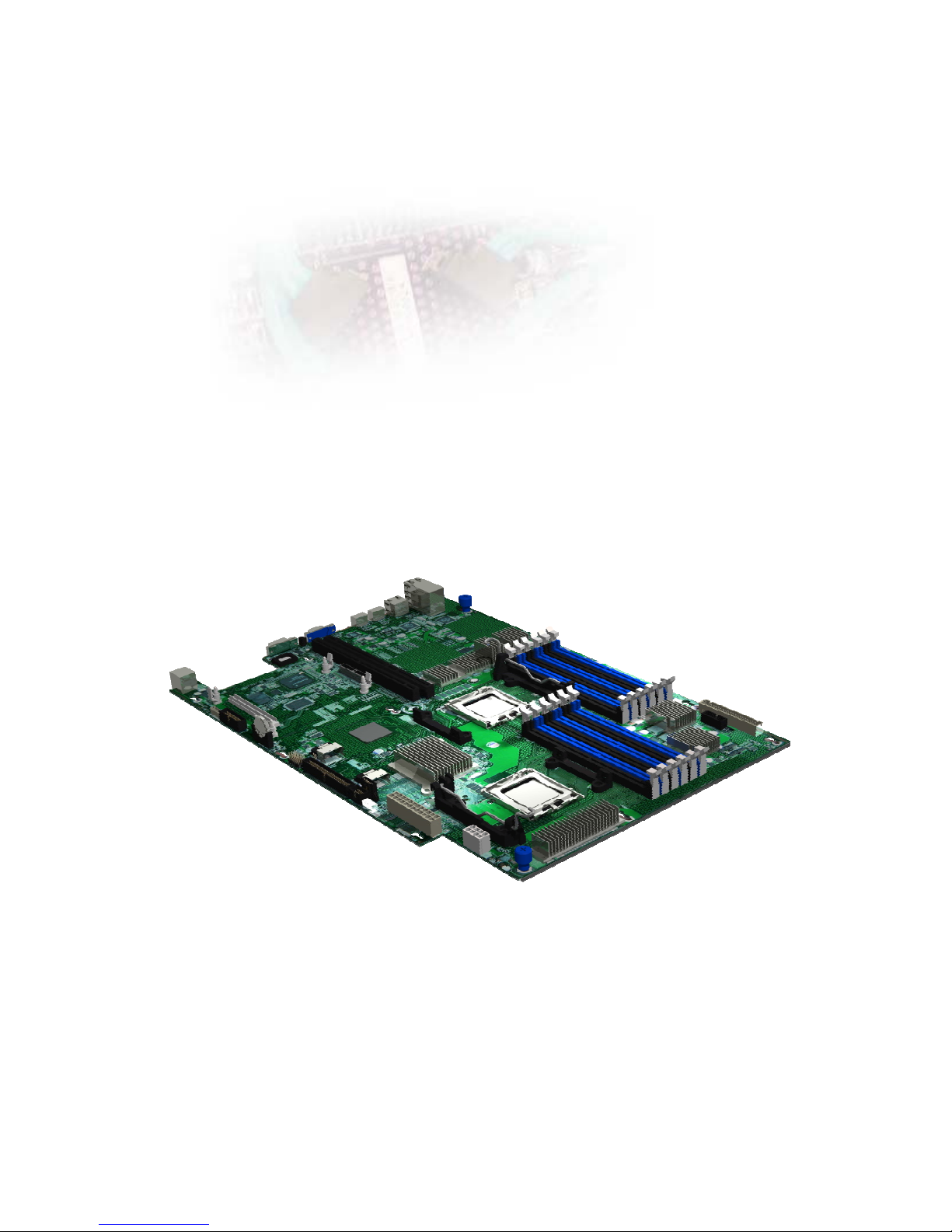
Figure 1-1 Motherboard Overview
This motherboard dimension is designed for 12” x 13”. The motherboard is configured to use nVIDIA
MCP55Pro, nVIDIA IO 55 (for 2U) and NEC PCI-X bridge uPD 720404 chipset. It supports dual AMD
®
Opteron™ 2000 series processors to accelerate even the most complicated server tasks. The following
highlights are the main features of the motherboard. For additional information, refer to this user manual.
Table 1-2 Product Features
Processor
Dual AMD
®
Opteron™ 2000 series processors
Supports 800MHz, 400MHz, 200MHz/1000MHz/600MHz Hyper
Transport Bus
Hyper -T ransport™ Technology Support
Located on two LGA 1207-pin sockets F
Chipset
System chip: nVIDIA MCP55Pro
C om pa n yin g c hi p: nV IDI A IO 55 (For 2U)
NEC PCI-X bridge uPD 720404
Memory
Twelve 240-pin DIMM vertical sockets
Supports up to 48GB of DDR2 667MHz
Supports ECC
Onboard LAN
Two GbE RJ45 ports (For 1U )
Four GbE RJ45 ports (For 2U)

Introduction
1230B0026701
1-3
N e t work controllers embedded in nVIDIA MCP55Pro and IO 55 (For
2U)
10/100/1000Mbps
Supports teaming, load-balancing, failover , TOE and jumbo frame
Onboard VGA
Embedded in Pilot SMC
Supports max 1280 x 1024 8 bpp, 1024 x 768 16 bpp
Integrated Super I/O
ServerEngine Pilot controller
Supports one fast UART 16550 serial port, one PS/2 keyboard port, and
one PS/2 mouse port
Expansion Slots
Expansion Slots (1U Chassis)
One PCI-E x16 slot with x8 speed or one PCI-X 64bit/100MHz slot
One PCI-E x8 slot with x4 speed
Expansion Slots (2U Chassis)
Two PCI-E x8 slots with x8 speed and one PCI-X 64bit/100MHz slot
Two PCI-E x8 slots with x8 speed and one PCI-E x8 slot with x4 speed
Daughter Cards
See Appendix in the Chassis User Manual
Introduction
1230B0026701
1-4
11..44 MMootthheerrbbooaarrdd LLaayyoouutt
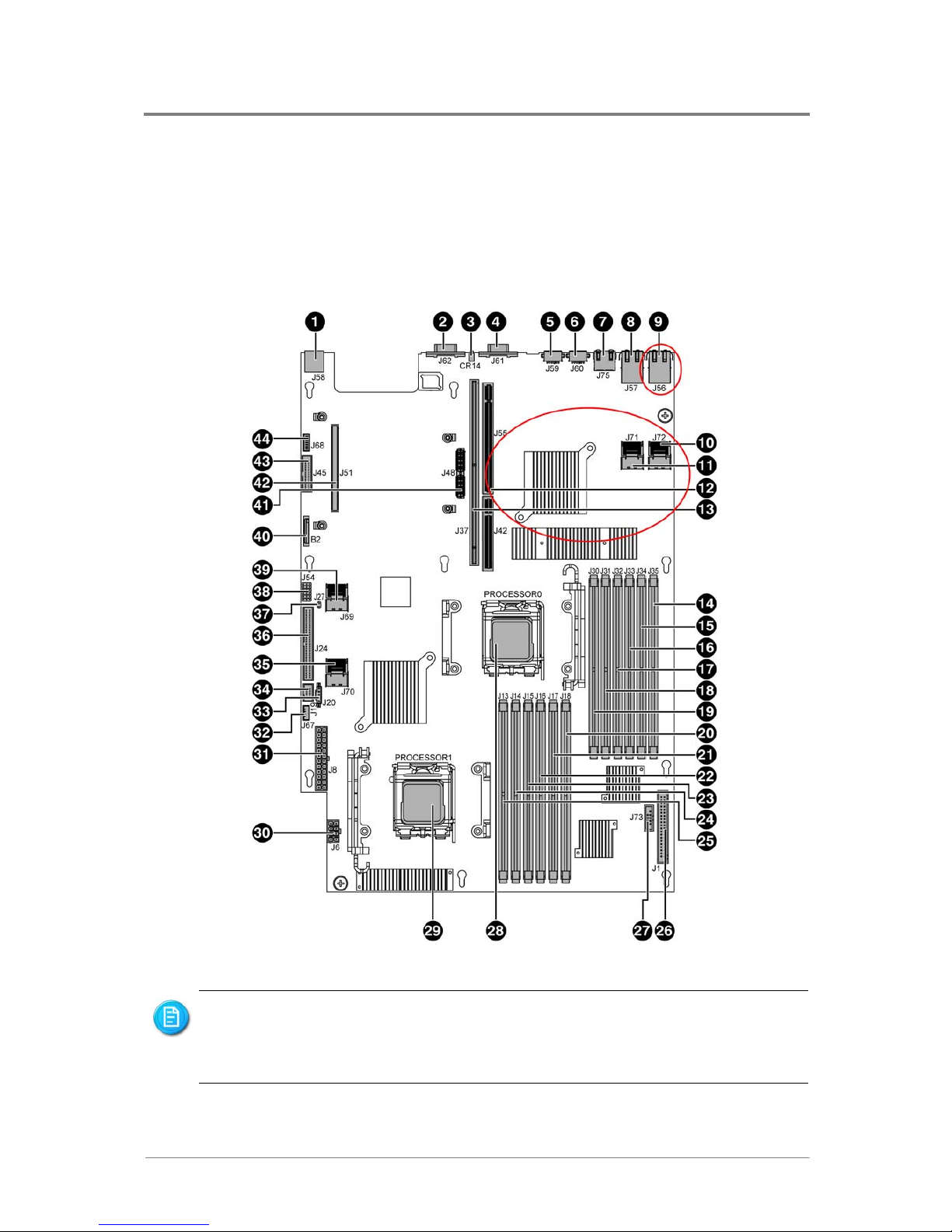
The layout of the motherboard is shown below. Each connector and major component is identified by the
number.
1.4.1 Connectors and Component Locations
Figure 1-2 Connectors and Component Locations
The words printed on the real motherboard to mark the processors are “CPU0” and
“CPU1”. Here just for consistency, the processors are marked with “PROCESSOR0”
and “PROCESSOR1” in the picture above.
The components indicated by red circles are not provided in 1U server.
Introduction
1230B0026701
1-5
Rear Dual USB Port (J58) DIMMA1 Socket for Processor 1 (J15)
Serial Port (J62) DIMMB0 Socket for Processor 1 (J14)
UID LED (CR14) DIMMA0 Socket for Processor 1 (J13)
D-sub VGA Port (J61) Fan Board Connector (J1)
PS/2 Mouse Port (J59) LCM Connector (Optional) (J73)
PS/2 Keyboard Port (J60) Processor 0 (CPU0)
Management Po r t (RJ 4 5) (J 75 ) Processor 1 (CPU1)
Dual NIC 1/2 Connector (RJ45) (J57) Processor Power Connector (J6)
Dual NIC 3/4 Connector (RJ45) (J56) Main Power Connector (J8)
Mini-SAS Connector 4 (4/5) (J72) Internal USB Port for USB Floppy (J67)
Mini-SAS Connector 3 (0/1/2/3) (J71) I2C (SMBus) Signal Connector for PSU (J20)
PCI-E x4 (x8) Expansion Slot (J55, J42) Front Panel USB Connector (J19)
PCI-X 100MHz/PCI-E x8 (x16) Expansion Slot (J37) Mini-SAS Connector 2 (4/5) (J70)
DIMMB2 Socket for Processor 0 (J35) Front Panel IDE Connector (J24)
DIMMA2 Socket for Processor 0 (J34) Chassis Intrusion Connector (J27)
DIMMB1 Socket for Processor 0 (J33) System Configuration Jumper (J54)
DIMMA1 Socket for Processor 0 (J32) Mini-SAS Connector 1 (0/1/2/3) (J69)
DIMMB0 Socket for Processor 0 (J31) Battery (B2)
DIMMA0 Socket for Processor 0 (J30) PCI-E Daughter Card Connector (J48)
DIMMB2 Socket for Processor 1 (J18) PCI-X Daughter Card Connector (J51)
DIMMA2 Socket for Processor 1 (J17) Floppy Connector (J45)
DIMMB1 Socket for Processor 1 (J16) Front Panel VGA Connector (J68)
Introduction
1230B0026701
1-6
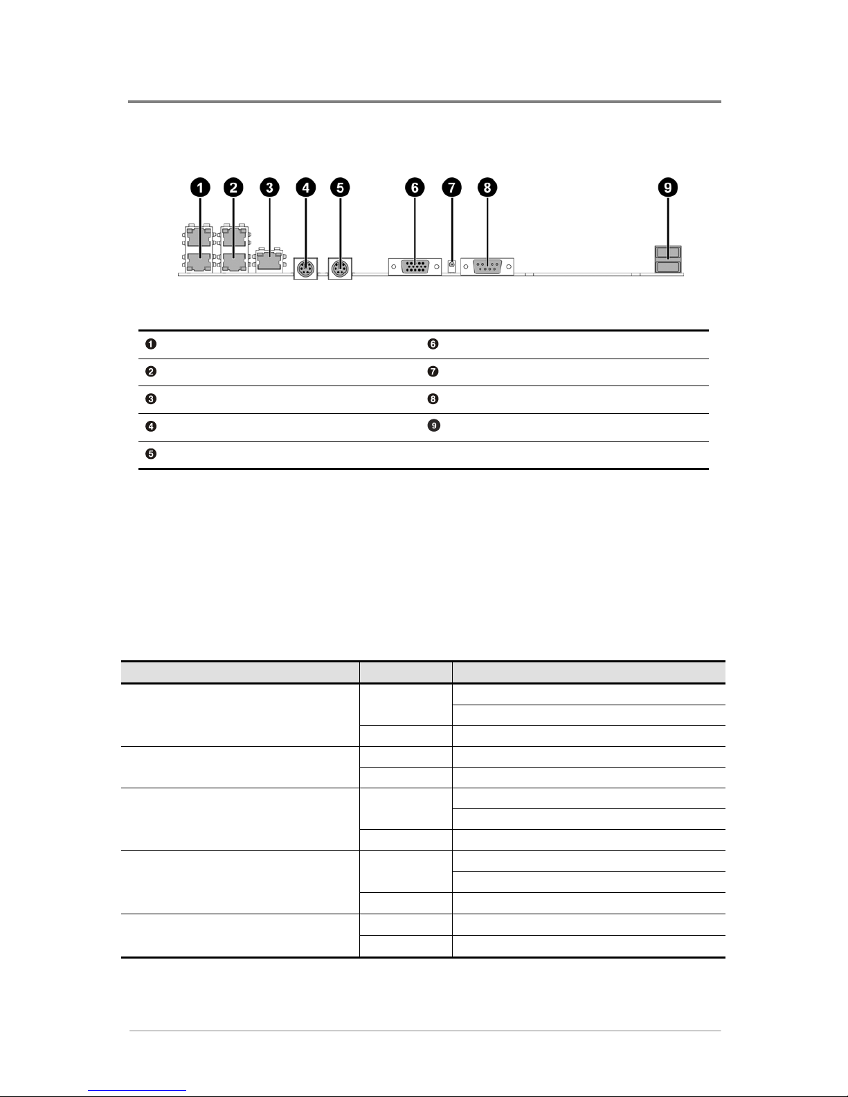
1.4.2 Back Panel Connectors
Figure 1-3 Back Panel Connectors
Dual NIC 3/4 Connector (RJ45) (For 2U) D-sub VGA Port
Dual NIC 1/2 Connector (RJ45) UID LED
Management Po r t (RJ 4 5) Serial Port
PS/2 Keyboard Port Rear Dual USB Port
PS/2 Mouse Port
1.4.3 System LED Information
The system LED Information introduces the UID LED, Power LED, NIC Link/Activity LED, NIC Speed
LED and so forth. Each NIC connector contains two LEDs that allow monitoring of network activity and
server identification.
Table 1-3 LED Information
Type of LED Color Status
On: UID bottom
Blue
Blinking: Chassis identify command
UID LED (CR14)
− Off: UID bottom
Green Blinking: BMC activity
BMC_LED_ACT (CR23)
− Off: BMC fail
On: Normal operating state
Blue
Blinking: System is in power saving states
Power LED
− Off: System is the off state
On: Linking on
Green
Blinking:
Accessing
NIC Link/Activity LED
− Off: No link
Amber
On: Linking at 1 Gbps speed
NIC Speed LED
−
Off: Others
Introduction
1230B0026701
1-7
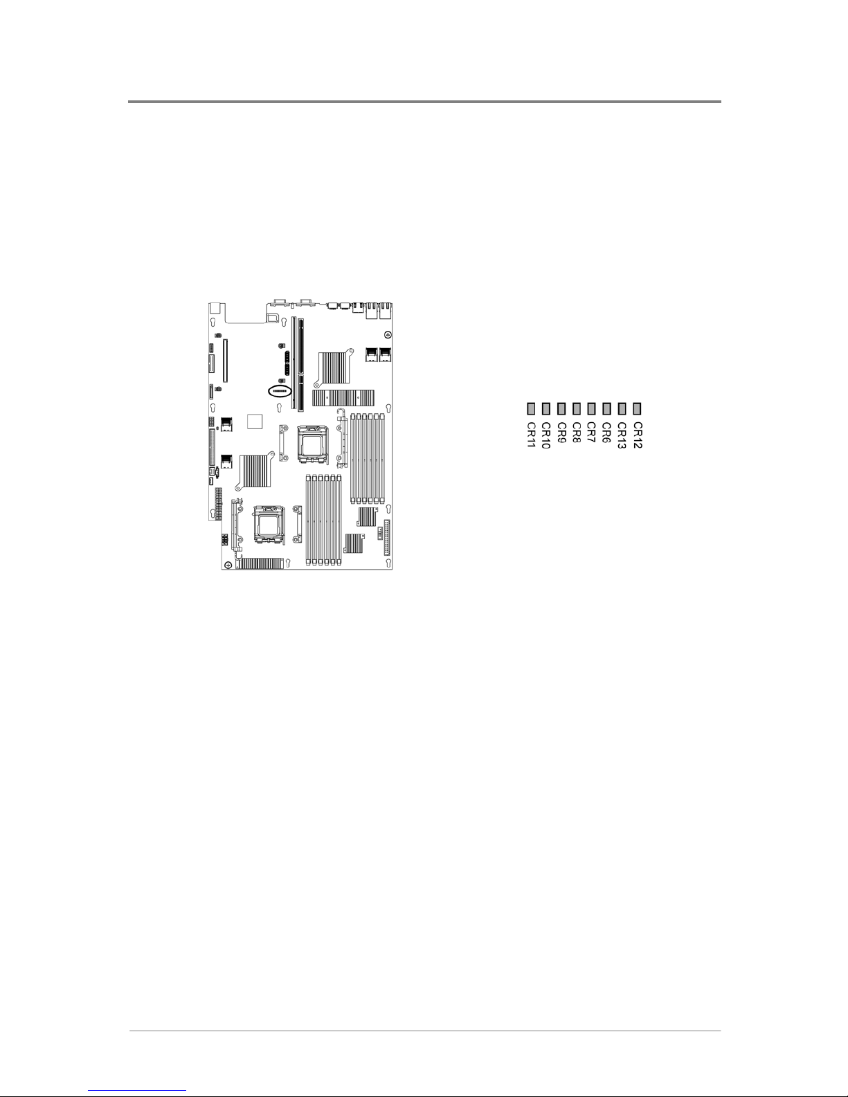
1.4.4 Port 80 LEDs Information
After opening the top cover, check the lights on the system board to verify if there is any component
failure. The system board contains Port 80 LEDs (with a total of eight), for you to determine where
errors take place. They are CR12, CR13, CR6, CR7, CR8, CR9, CR10 and CR11. All LEDs will be
cleared and restored to normal status after the server is power cycled.
The location of Port 80 LEDs is shown as below:
Figure 1-4 Port 80 LEDs
There are total of eight LEDs which are divided into two groups. LEDs from CR12 to CR7 are in one
group, and the other four are in another group. The two groups represent two digits of the hex code. The
group comprised of CR8-CR11 stands for the first digit of the hex code. The group comprised of
CR12-CR7 stands for the second digit of the hex code. In the “Table 1-4 Code Information”, “0” stands
for LED off, while “1” stands for LED on. According to the LED status of Port 80 LEDs, the
corresponding hex code can be obtained by the user. From the “Table 1-7 POST Code Information”, the
user can find out where an error takes place. For example, if a hex code 0B is obtained, the user can
know that the server cannot detect the PS/2 mouse. The user can then take measures, such as reinserting
a mouse, to solve the problem.
Introduction
1230B0026701
1-8
Table 1-4 Code Information
Hex
Code
CR11 CR10 CR9 CR8
Hex
Code
CR7 CR6 CR13 CR12
8 4 2 1
8 4 2 1
0
0 0 0 0
0
0 0 0 0
1
0 0 0 1
1
0 0 0 1
2
0 0 1 0
2
0 0 1 0
3
0 0 1 1
3
0 0 1 1
4
0 1 0 0
4
0 1 0 0
5
0 1 0 1
5
0 1 0 1
6
0 1 1 0
6
0 1 1 0
7
0 1 1 1
7
0 1 1 1
8
1 0 0 0
8
1 0 0 0
9
1 0 0 1
9
1 0 0 1
A
1 0 1 0
A
1 0 1 0
B
1 0 1 1
B
1 0 1 1
C
1 1 0 0
C
1 1 0 0
D
1 1 0 1
D
1 1 0 1
E
1 1 1 0
E
1 1 1 0
F
1 1 1 1
F
1 1 1 1
Table 1-5 Boot Block Initialization Code Checkpoints
Checkpoint Description
Before D1 Early chipset initialization is done. Early super I/O initialization is done including
RTC and keyboard controller. NMI is disabled.
D1 Perform keyboard controller BAT test. Check if waking up from power management
suspend state. Save power-on CPUID value in scratch CMOS.
D0 Go to flat mode with 4GB limit and GA20 enabled. Verify the bootblock checksum.
D2 Disable CACHE before memory detection. Execute full memory sizing module.
Verify that flat mode is enabled.
D3 If memory sizing module not executed, start memory refresh and do memory sizing
in Bootblock code. Do additional chipset initialization. Re-enable CACHE. Verify
that flat mode is enabled.
D4 Test base 512KB memory. Adjust policies and cache first 8MB. Set stack.
Introduction
1230B0026701
1-9
Checkpoint Description
D5 Bootblock code is copied from ROM to lower system memory and control is given to
it. BIOS now executes out of RAM.
D6 Both key sequence and OEM specific method is checked to determine if BIOS
recovery is forced. Main BIOS checksum is tested. If BIOS recovery is necessary,
control flows to checkpoint E0. See Bootblock Recovery Code Checkpoints section
of document for more information.
D7 Restore CPUID value back into register. The Bootblock-Runtime interface module is
moved to system memory and control is given to it. Determine whether to execute
serial flash.
D8 The Runtime module is uncompressed into memory. CPUID information is stored in
memory.
D9 Store the Uncompressed pointer for future use in PMM. Copying Main BIOS into
memory. Leaves all RAM below 1MB Read-Write including E000 and F000 shadow
areas but closing SMRAM.
DA Restore CPUID value back into register. Give control to BIOS POST
(ExecutePOSTKernel). See POST Code Checkpoints section of document for more
information.
Table 1-6 Bootblock Recovery Code Checkpoints
Checkpoint Description
E0 Initialize the floppy controller in the super I/O. Some interrupt vectors are initialized.
DMA controller is initialized. 8259 interrupt controller is initialized. L1 cache is
enabled.
E9 Set up floppy controller and data. Attempt to read from floppy.
EA Enable ATAPI hardware. Attempt to read from ARMD and ATAPI CDROM.
EB Disable ATAPI hardware. Jump back to checkpoint E9.
EF Read error occurred on media. Jump back to checkpoint EB.
E9 or EA Determine information about root directory of recovery media.
F0 Search for pre-defined recovery file name in root directory.
F1 Recovery file not found.
F2 Start reading FAT table and analyze FAT to find the clusters occupied by the
recovery file.
F3 Start reading the recovery file cluster by cluster.
F5 Disable L1 cache.

Introduction
1230B0026701
1-10
Checkpoint Description
FA Check the validity of the recovery file configuration to the current configuration of
the flash part.
FB Make flash write enabled through chipset and OEM specific method. Detect proper
flash part. Verify that the found flash part size equals the recovery file size.
F4 The recovery file size does not equal the found flash part size.
FC Erase the flash part.
FD Program the flash part.
FF The flash has been updated successfully. Make flash write disabled. Disable ATAPI
hardware. Restore CPUID value back into register. Give control to F000 ROM at
F000:FFF0h.
Table 1-7 POST Code Information
Checkpoint Description
03 Disable NMI, Parity, video for EGA and DMA controllers. Initialize BIOS, POST,
and Runtime data area. Also initialize BIOS modules on POST entry and GPNV area.
Initialize CMOS as mentioned in the Kernel Variable "wCMOSFlags".
04 Check CMOS diagnostic byte to determine if battery power is OK and CMOS
checksum is OK. Verify CMOS checksum manually by reading storage area. If the
CMOS checksum is bad, update CMOS with power-on default values and clear
passwords. Initialize status register A.
Initialize data variables that are based on CMOS setup questions. Initialize both the
8259 compatible PICs in the system
05 Initialize the interrupt controlling hardware (generally PIC) and interrupt vector table.
06 Do R/W test to CH-2 count reg. Initialize CH-0 as system timer. Install the
POSTINT1Ch handler. Enable IRQ-0 in PIC for system timer interrupt.
Trap INT1Ch vector to "POSTINT1ChHandlerBlock".
08 Initialize the CPU. The BAT test is being done on KBC. Program the keyboard
controller command byte is being done after Auto detection of KB/MS using AMI
KB-5.
C0 Early CPU Init Start -- Disable Cache - Init Local APIC
C1 Set up boot strap processor information
C2 Set up boot strap processor for POST
C5 Enumerate and set up application processors
C6 Re-enable cache for boot strap processor

Introduction
1230B0026701
1-11
Checkpoint Description
C7 Early CPU Init Exit
0A Initialize the 8042 compatible Key Board Controller.
0B Detect the presence of PS/2 mouse.
0C Detect the presence of Keyboard in KBC port.
0E Testing and initialization of different Input Devices. Also, update the Kernel
Variables.
Trap the INT09h vector, so that the POST INT09h handler gets control for IRQ1.
Uncompress all available language, BIOS logo, and Silent logo modules.
13 Early POST initialization of chipset registers.
24 Uncompress and initialize any platform specific BIOS modules.
30 Initialize System Management Interrupt.
2A Initialize different devices through DIM.
See DIM Code Checkpoints section of document for more information.
2C Initialize different devices. Detects and initializes the video adapter installed in the
system that has optional ROMs.
2E Initialize all the output devices.
31 Allocate memory for ADM module and uncompress it. Give control to ADM module
for initialization. Initialize language and font modules for ADM. Activate ADM
module.
33 Initialize the silent boot module. Set the window for displaying text information.
37 Displaying sign-on message, CPU information, setup key message, and any OEM
specific information.
38 Initialize different devices through DIM.
39 Initialize DMAC-1 & DMAC-2.
3A Initialize RTC date/time.
3B Test for total memory installed in the system. Also, Check for DEL or ESC keys to
limit memory test. Display total memory in the system.
3C Mid POST initialization of chipset registers.
40 Detect different devices (Parallel ports, serial ports, and coprocessor in CPU, etc.)
successfully installed in the system and update the BDA, EBDA, etc.
50 Programming the memory hole or any kind of implementation that needs an
adjustment in system RAM size if needed.

Introduction
1230B0026701
1-12
Checkpoint Description
52 Update CMOS memory size from memory found in memory test. Allocates memory
for Extended BIOS Data Area from base memory.
60 Initialize NUM-LOCK status and programs the KBD typematic rate.
75 Initialize Int-13 and prepare for IPL detection.
78 Initialize IPL devices controlled by BIOS and option ROMs.
7A Initialize remaining option ROMs.
7C Generate and write contents of ESCD in NVRam.
84 Log errors encountered during POST.
85 Display errors to the user and gets the user response for error.
87 Execute BIOS setup if needed / requested.
8C Late POST initialization of chipset registers.
8D Build ACPI tables (if ACPI is supported)
8E Program the peripheral parameters. Enable/Disable NMI as selected
90 Late POST initialization of system management is interrupted.
A0 Check boot password if installed.
A1 Clean-up work needed before booting to OS.
A2 Take care of runtime image preparation for different BIOS modules. Fill the free area
in F000h segment with 0FFh. Initializes the Microsoft IRQ Routing Table. Prepares
the runtime language module. Disables the system configuration display if needed.
A4 Initialize runtime language module.
A7 Display the system configuration screen if enabled. Initialize the CPU’s before boot,
which includes the programming of the MTRR’s.
A8 Prepare CPU for OS boot including final MTRR values.
A9 Wait for user input at configure display if needed.
AA Uninstall POST INT1Ch vector and INT09h vector. Reinitialize the ADM module.
AB Prepare BBS for Int 19 boot.
AC End of POST initialization of chipset registers.
B1 Save system context for ACPI.
00 Pass control to OS Loader (typically INT19h).

Introduction
1230B0026701
1-13
Table 1-8 DIM Code Checkpoints
Checkpoint Description
2A Initialize different buses and perform the following functions: Reset, Detect, and
Disable (function 0); Static Device Initialization (function 1); Boot Output Device
Initialization (function 2). Function 0 disables all device nodes, PCI devices, and PnP
ISA cards. It also assigns PCI bus numbers. Function 1 initializes all static devices
that include manual configured onboard peripherals, memory and I/O decode
windows in PCI-PCI bridges, and noncompliant PCI devices. Static resources are also
reserved. Function 2 searches for and initializes any PnP, PCI, or AGP video devices.
38
Initialize different buses and perform the following functions: Boot Input Device
Initialization (function 3); IPL Device Initialization (function 4); General Device
Initialization (function 5). Function 3 searches for and configures PCI input devices
and detects if system has standard keyboard controller. Function 4 searches for and
configures all PnP and PCI boot devices. Function 5 configures all onboard
peripherals that are set to an automatic configuration and configures all remaining
PnP and PCI devices.
Table 1-9 ACPI Runtime Checkpoints
Checkpoint Description
AC First ASL check point. Indicates the system is running in ACPI mode.
AA System is running in APIC mode.
01, 02, 03,
04, 05
Entering sleep state S1, S2, S3, S4, or S5.
10, 20, 30,
40, 50
Waking from sleep state S1, S2, S3, S4, or S5.
Table 1-10 Beep Codes
Number of Beeps Description
1 Memory refresh timer error.
2 Parity error
3 Main memory read / write test error.
4 Motherboard timer not operational
5 Processor error
6 Keyboard controller BAT test error.
7 General exception error.
8 Display memory error.
9 ROM checksum error
10 CMOS shutdown register read/write error

Introduction
1230B0026701
1-14
Number of Beeps Description
11 Cache memory bad
Table 1-11 Troubleshooting BIOS Beep Codes
Number of Beeps Description
1, 2 or 3 Reseat the memory, or replace with known good modules.
4-7, 9-11 Fatal error indicating a serious problem with the system. Consult your system
manufacturer.
Before declaring the motherboard beyond all hope, eliminate the possibility of
interference by a malfunctioning add-in card. Remove all expansion cards
cards except the video adapter.
If the beep codes are generated even when all other expansion cards are absent,
the motherboard has a serious problem. Consult your system manufacturer.
If the beep codes are not generated when all other expansion cards are absent,
one of the add-in cards is causing the malfunction. Insert the cards back into
the system one at a time until the problem happens again. This will reveal the
malfunctioning add-in card.
8 If the system video adapter is an add-in card, replace or reseat the video
adapter. If the video adapter is an integrated part of the system board, the
board may be faulty.

Chapter 2
Hardware
Operations
Before You Start
Screw Holes
Battery
Processor
System Memory
System Configuration Jumper
Hardware Operations
1230B0026701
2-1
22 HHaarrddwwaarree OOppeerraattiioonnss
This chapter provides the detailed information and removal steps for motherboard, including battery,
processor, system memory, and jumpers.
22..11 BBeeffoorree YYoouu SSttaarrtt
Take note of the following precautions before you remove or install any components on the motherboard.
The server does not completely power off when the front panel power button is pressed. The button
toggles server power between On and Standby. In Standby, the server removes power from most
electronics and drives, while portions of the power supply and some internal circuitry remain active. To
completely remove all power supplies from the system, disconnect the power cords from the server.
Moving the Power On/Off switch to the Off position does not completely remove system
power. Some portions of the power supply and some internal circuitry remain active.
Disconnect all power cords from the server to remove all power from the system.
To power off the server, please refer to “2.1.1 Power Off” in the Chassis User Manual.
The components shown in this chapter are mainly for your reference. Please take the actual
shipment as standard.
To reduce the risk of injury from electric shock, remove the power cord to completely
disconnect power from the system.
Hardware Operations
1230B0026701
2-2
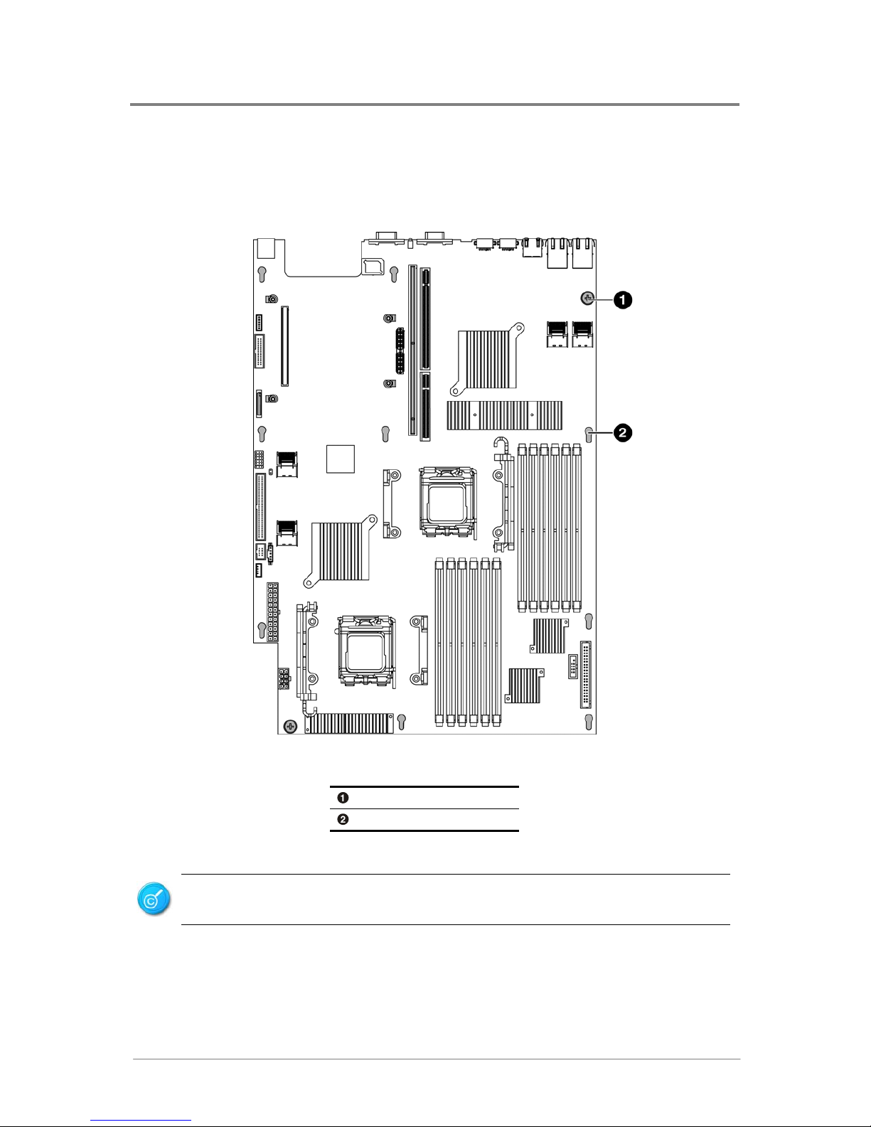
22..22 SSccrreeww HHoolleess
The motherboard is designed with totally nine locking tab holes and two thumbscrews as the picture
shows.
Figure 2-1 Screws Placement
Thumbscrew
Locking Tab Hole
Do not overly tighten the thumbscrews. Doing so may damage the motherboard.
Hardware Operations
1230B0026701
2-3
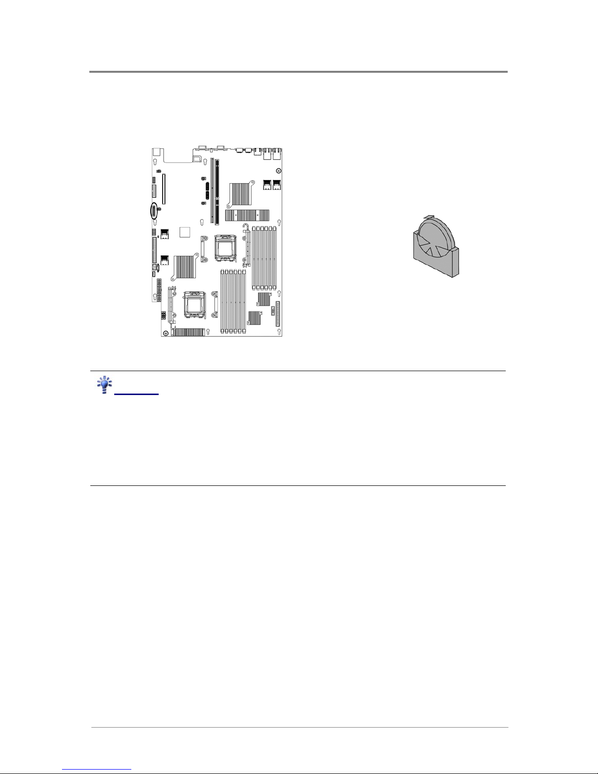
22..33 BBaatttteerryy
The location of battery is shown below:
Figure 2-2 Battery Location
Reminder
Before you remove or install the battery, please follow the steps below:
Step 1: Make sure the server is not turned on or connected to the AC power. To power off the server,
see “2.1.1 Power Off” in the Chassis User Manual.
Step 2: Remove the chassis cover. To remo ve the cover, see “2.2 Chassis Cover” in the Chassis User
Manual.
Step 3: Disconnect all necessary cable connections.
Hardware Operations
1230B0026701
2-4
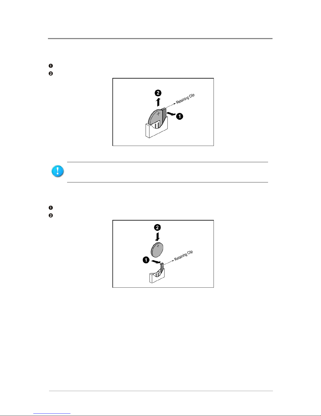
2.3.1 To remove the battery
Pull the battery retaining clip away from the battery.
Lift the battery on the lever side and pull it out of the holder.
Figure 2-3 Pulling the Battery out of the Holder
Do not bend the retaining clip during battery replacement. For proper operation, the clip
must maintain a position of contact with the battery.
2.3.2 To install the battery
Pull the battery retaining clip away.
Put the battery into the holder.
Figure 2-4 Putting the Battery into the Holder
Hardware Operations
1230B0026701
2-5
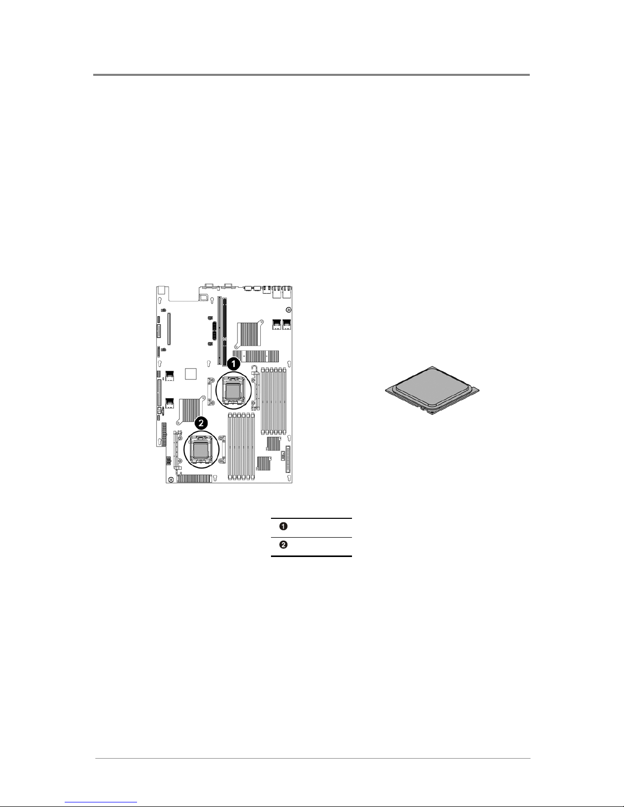
22..44 PPrroocceessssoorr
The motherboard supports dual AMD® Opteron™ 2000 series processors. With two 1207-pin LGA
sockets F, the system can be configured to either single or dual processors system to connect to the
nVIDIA MCP 55Pro through the Hyper Transport Bus. The AMD
®
Opteron™ 2000 series processor
supports three link frequency groups:
• 800MHz, 400MHz, 200MHz
• 1000MHz
• 600MHz
The location of the processors on the motherboard is shown below:
Figure 2-5 Processor Location
Processor 0
Processor 1
You can install single or dual processors on the motherboard according to your own needs.
1. If SINGLE processor is intended, recommend that you install the processor on the processor 0 socket,
please refer to the figure above.
2. If install DUAL processors, use the same type of processor running at the same frequency.
Hardware Operations
1230B0026701
2-6
Before you install or remove the processor, make sure the power is off. To power off the
server, see “2.1.1 Power Off” in the Chassis User Manual.
Reminder
Before you remove or install heat sink, processor or heat sink socket, please follow the steps below:
Step 1: Make sure the server is not turned on or connected to the AC power. To power off the server,
see “2.1.1 Power Off” in the Chassis User Manual.
Step 2: Remove the chassis cover. To remo ve the cover, see “2.2 Chassis Cover” in the Chassis User
Manual.
Step 3: Disconnect all necessary cable connections.
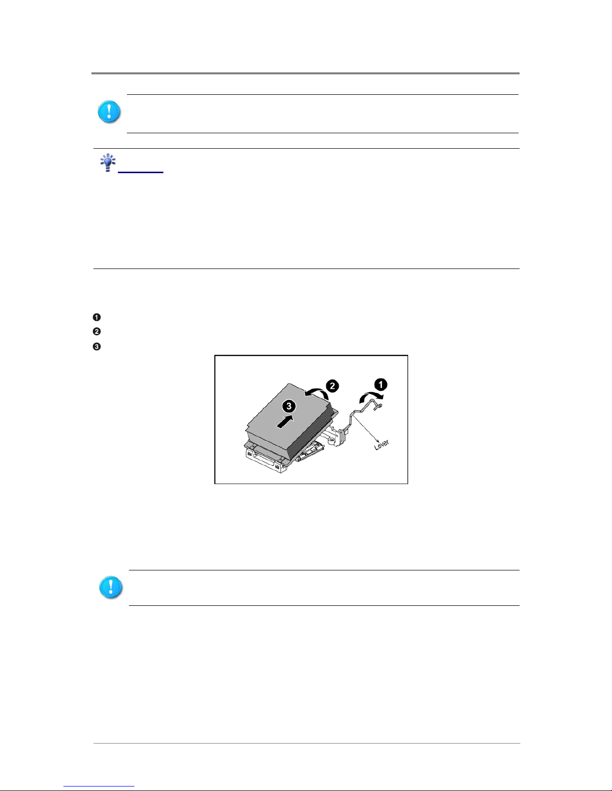
2.4.1 To remove the heat sink
Rotate to release the lever.
Tilt the heat sink.
Pull up the heat sink from the installed processor.
Figure 2-6 Pulling up the Heat Sink
2.4.2 To install the heat sink
Reverse the steps above to install the heat sink.
Before you put the heat sink on top of the installed processor, please do not forget to check if
the grease is complete on bottom of the heat sink.
Hardware Operations
1230B0026701
2-7
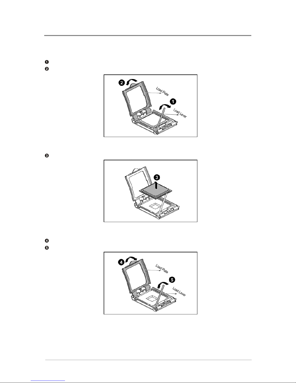
2.4.3 To remove the processor
Unlock the load lever and lift it up.
Open the load plate.
Figure 2-7 Opening the Load Plate
Lift the processor out of the socket.
Figure 2-8 Lifting the Processor out of the Socket
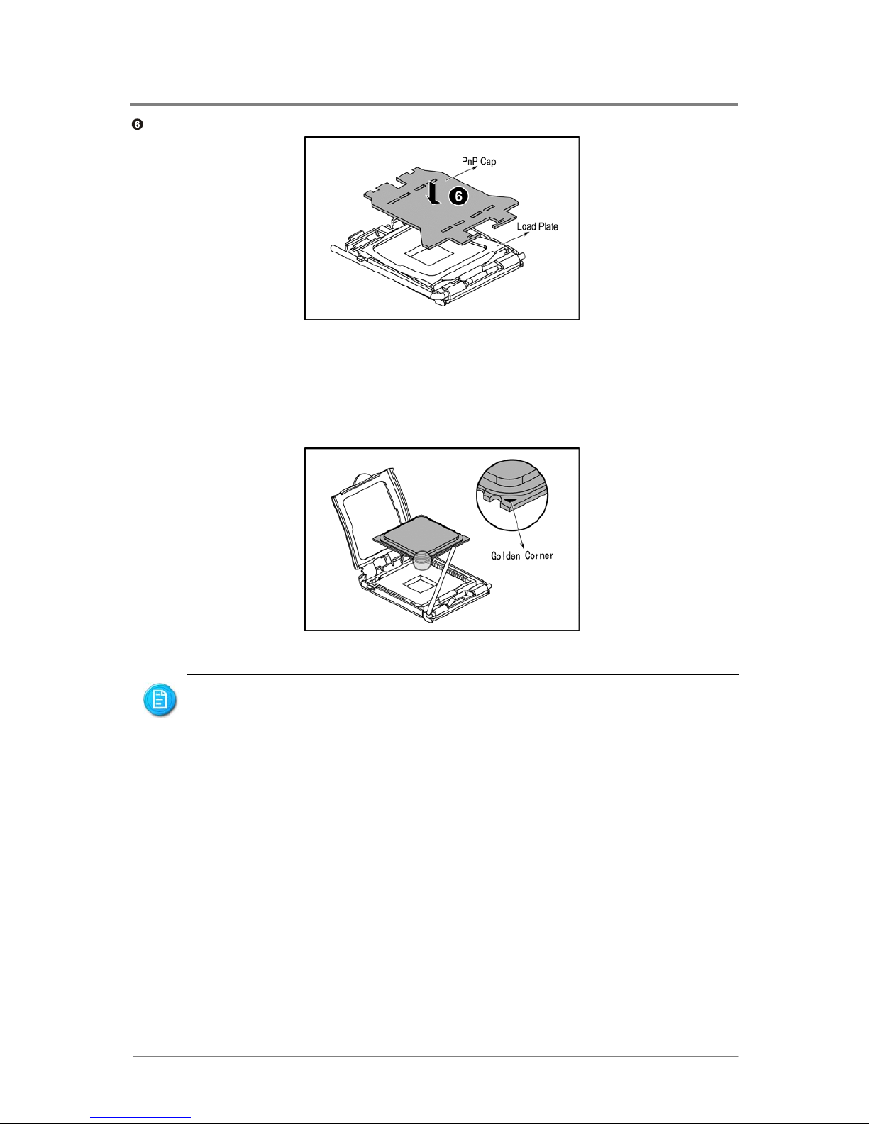
Close the load plate.
Lock the load lever.
Figure 2-9 Closing the Load Plate
Hardware Operations
1230B0026701
2-8
Place the PnP cap onto the load plate.
Figure 2-10 Placing on the PnP Cap
2.4.4 To install the processor
Reverse the steps above to install the processor. However, when inserting the processor into the socket,
make sure that the golden corner on the processor is aimed at the socket as picture shows:
Figure 2-11 Aiming the Golden Corner at the Socket
When the processor is in place, press it firmly on the socket while you push down the
socket lever to secure the processor. The lever clicks on the socket indicating that it is
locked.
The processor fits only in one orientation. Do not force the processor into the socket to
avoid bending the pins and damaging the processor. If the processor does not fit
completely, check its orientation or check for bent pins.
Hardware Operations
1230B0026701
2-9
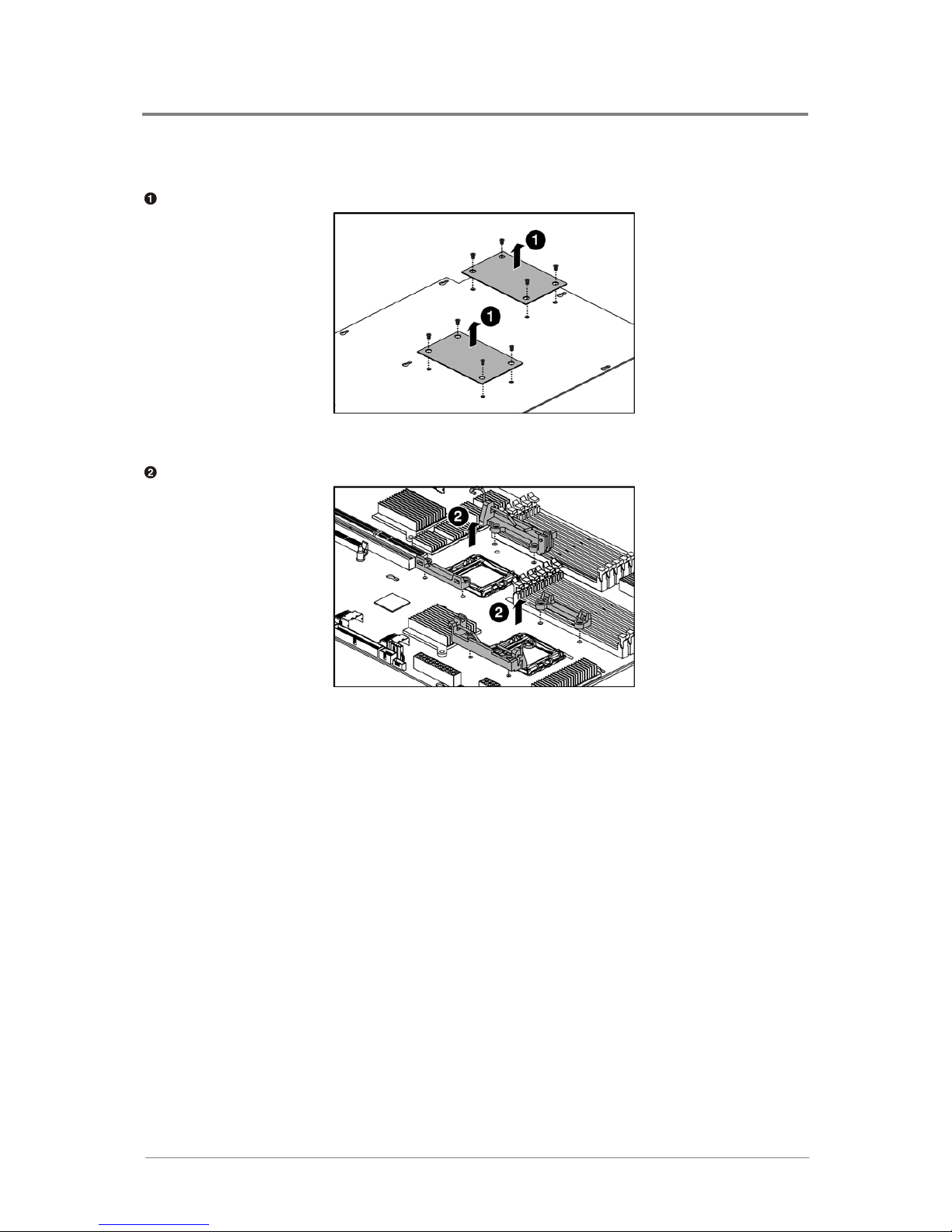
2.4.5 To remove the heat sink socket
Remove the heat sink base socket from the bottom of the motherboard.
Figure 2-12 Removing the Heat Sink Base Socket
Lift the heat sink socket up from the motherboard.
Figure 2-13 Lifting up the Heat Sink Socket
2.4.6 To install the heat sink socket
Reverse the steps above to install the heat sink socket.

Hardware Operations
1230B0026701
2-10
22..55 SSyysstteemm MMeemmoorryy
The motherboard supports twelve DDR2 667MHz vertical DIMMs to provide up to 48GB with ECC
support. The 667MHz differential memory clocks are driven by the AMD processor with length
matching and impedance controlled through all the DIMM slots.
1U Chassis only support low-profile or Ultra low-profile DIMM.
The location of the DIMM sockets on the motherboard is shown below:
Figure 2-14 System Memory Location
2.5.1 DIMM Population
There are two groups of DIMMs, six in each group on the motherboard to support the processor0 and
processor1 correspondingly. The twelve DIMM sockets are respectively processor0 DIMMA0,
processor0 DIMMB0, processor0 DIMMA1, processor0 DIMMB1, processor0 DIMMA2, processor0
DIMMB2; and processor1 DIMMA0, processor1 DIMMB0, processor1 DIMMA1, processor1 DIMMB1,
processor1 DIMMA2, processor1 DIMMB2. When you insert the DIMM(s), you have to always start
with DIMMA2 and DIMMB2 as a pair.

Hardware Operations
1230B0026701
2-11
For the location of each DIMM socket, please refer to “1.4.1 Connectors and Component Locations” and
the following table:
1. If only install one SINGLE processor, please refer to the following table to install the DIMMs.
Table 2-1 DIMM Installation Option 1
DIMM Processor DIMMA0 DIMMB0 DIMMA1 DIMMB1 DIMMA2 DIMMB2
Total Memory Size
─ ─ ─ ─ 512MB 512MB 1GB
─ ─ ─ ─ 1GB 1GB 2GB
─ ─ ─ ─ 2GB 2GB 4GB
2 Processor 0
─ ─ ─ ─ 4GB 4GB 8GB
─ ─
512MB 512MB 512MB
512MB 2GB
─ ─ 1GB 1GB 1GB 1GB 4GB
─ ─ 2GB 2GB 2GB 2GB 8GB
4 Processor 0
─ ─ 4GB 4GB 4GB 4GB 16GB
*512MB *512MB *512MB *512MB *512MB *512MB 3GB
*1GB *1GB *1GB *1GB *1GB *1GB 6GB
*2GB *2GB *2GB *2GB *2GB *2GB 12GB
6 Processor 0
*4GB *4GB *4GB *4GB *4GB *4GB 24GB

Hardware Operations
1230B0026701
2-12
2. If install DUAL processors, please refer to the following table to install the DIMMs.
T ab le 2-2
DIMM Installation Option 2
DIMM Processor DIMMA0 DIMMB0 DIMMA1 DIMMB1 DIMMA2 DIMMB2
Total Memory Size
Processor 0
─
─
─
─
512MB 512MB
Processor 1
─
─
─
─
512MB 512MB
2GB
Processor 0
─
─
─
─
1GB 1GB
Processor 1
─
─
─
─
1GB 1GB
4GB
Processor 0
─
─
─
─
2GB 2GB
Processor 1
─
─
─
─
2GB 2GB
8GB
Processor 0
─
─
─
─
4GB 4GB
4
Processor 1
─
─
─
─
4GB 4GB
16GB
Processor 0
─
─
512MB 512MB 512MB
512MB
Processor 1
─
─
512MB 512MB 512MB
512MB
4GB
Processor 0
─
─
1GB 1GB 1GB
1GB
Processor 1
─
─
1GB 1GB 1GB
1GB
8GB
Processor 0
─
─
2GB 2GB 2GB
2GB
Processor 1
─
─
2GB 2GB 2GB
2GB
16GB
Processor 0
─
─
4GB 4GB 4GB
4GB
8
Processor 1
─
─
4GB 4GB 4GB
4GB
32GB
Processor 0
*512MB *512MB *512MB
*512MB *512MB
*512MB
Processor 1
*512MB *512MB *512MB
*512MB *512MB
*512MB
6GB
Processor 0
*1GB *1GB *1GB
*1GB *1GB
*1GB
Processor 1
*1GB *1GB *1GB
*1GB *1GB
*1GB
12GB
Processor 0
*2GB *2GB *2GB
*2GB *2GB
*2GB
Processor 1
*2GB *2GB *2GB
*2GB *2GB
*2GB
24GB
Processor 0
*4GB *4GB *4GB
*4GB *4GB
*4GB
12
Processor 1
*4GB *4GB *4GB
*4GB *4GB
*4GB
48GB
The empty DIMM socket is marked as “”.
All the DIMMs installed must be at the same speed.
In the table of DIMM installation option 1 and 2, the DIMMs carrying “*” will run at
a lower frequency of 533MHz.

Hardware Operations
1230B0026701
2-13
Reminder
Before you remove or install any DIMMs, please follow the steps below:
Step 1: Make sure the server is not turned on or connected to the AC power. To power off the server,
see “2.1.1 Power Off” in the Chassis User Manual.
Step 2: Remove the chassis cover. To remo ve the cover, see “2.2 Chassis Cover” in the Chassis User
Manual.
Step 3: Disconnect all the necessary cable connections.
2.5.2 To remove a DIMM
Unlock a DIMM socket by pressing the retaining clips outward. This action releases the module and
partially lifts it out of the socket.
Lift out the DIMM.
Figure 2-15 Lifting the DIMM out of the Socket

Hardware Operations
1230B0026701
2-14
2.5.3 To install a DIMM
Unlock a DIMM socket by pressing the retaining clips outward.
Figure 2-16 Pressing the Retaining Clips Outward
Aim the notch on the memory at the break on the socket. Carefully insert the DIMM into the socket
until the retaining clips snap back in place.
Figure 2-17 Inserting the DIMM into the Socket
DIMMs fit in only one direction. DO NOT force a DIMM into the socket to avoid
damaging the DIMM.

Hardware Operations
1230B0026701
2-15
22..66 SSyysstteemm CCoonnffiigguurraattiioonn JJuummppeerr
The motherboard involves one jumper, system configuration jumper. The system configuration jumper is
divided into six pin groups (refer to “3.20 System Configuration Jumper Setting”).
The location of system configuration jumper on the motherboard is shown below:
Figure 2-18 System Configuration Jumper Location

Chapter 3
Connectors and
Jumper
Power Connectors
Front Panel IDE Connector
Floppy Connector
Chassis Intrusion Connector
Front Panel VGA Connector
D-sub VGA Port
Serial Port
Keyboard and Mouse Ports
Rear Dual USB Port
Front Panel USB Connector
I2C (SMBus) Signal Connector for PSU
Two Dual NIC Connectors (RJ45)
Management Port (RJ45)
Fan Board Connector
Mini-SAS Connectors
LCM Connector (Optional)
Internal USB Port for USB Floppy
System Configuration Jumper Setting
Connectors and Jumper
1230B0026701
3-1
33 CCoonnnneeccttoorrss aanndd JJuummppeerr
The locations of all the connectors described in this chapter are shown in “1.4.1 Connectors and
Component Locations”.
“Key” stands for foolproof feature; “NC” stands for unused.
33..11 PPoowweerr CCoonnnneeccttoorrss ((JJ88,, JJ66))
The main power supply connection is obtained using the 24-pin connector (only the first 20 pins are
populated when using an ATX12V power supply).
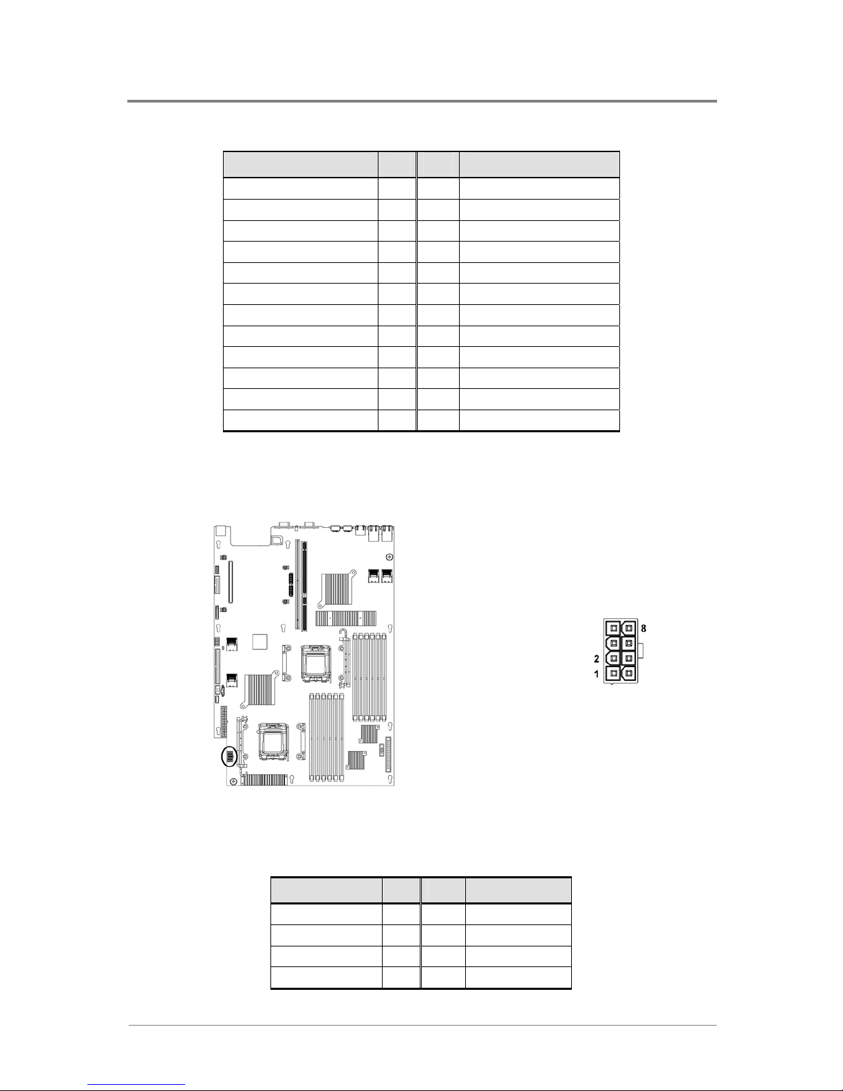
The processor power supply connection is obtained using the 8-pin connector (only the first 4 pins are
populated when using an ATX12V power supply).
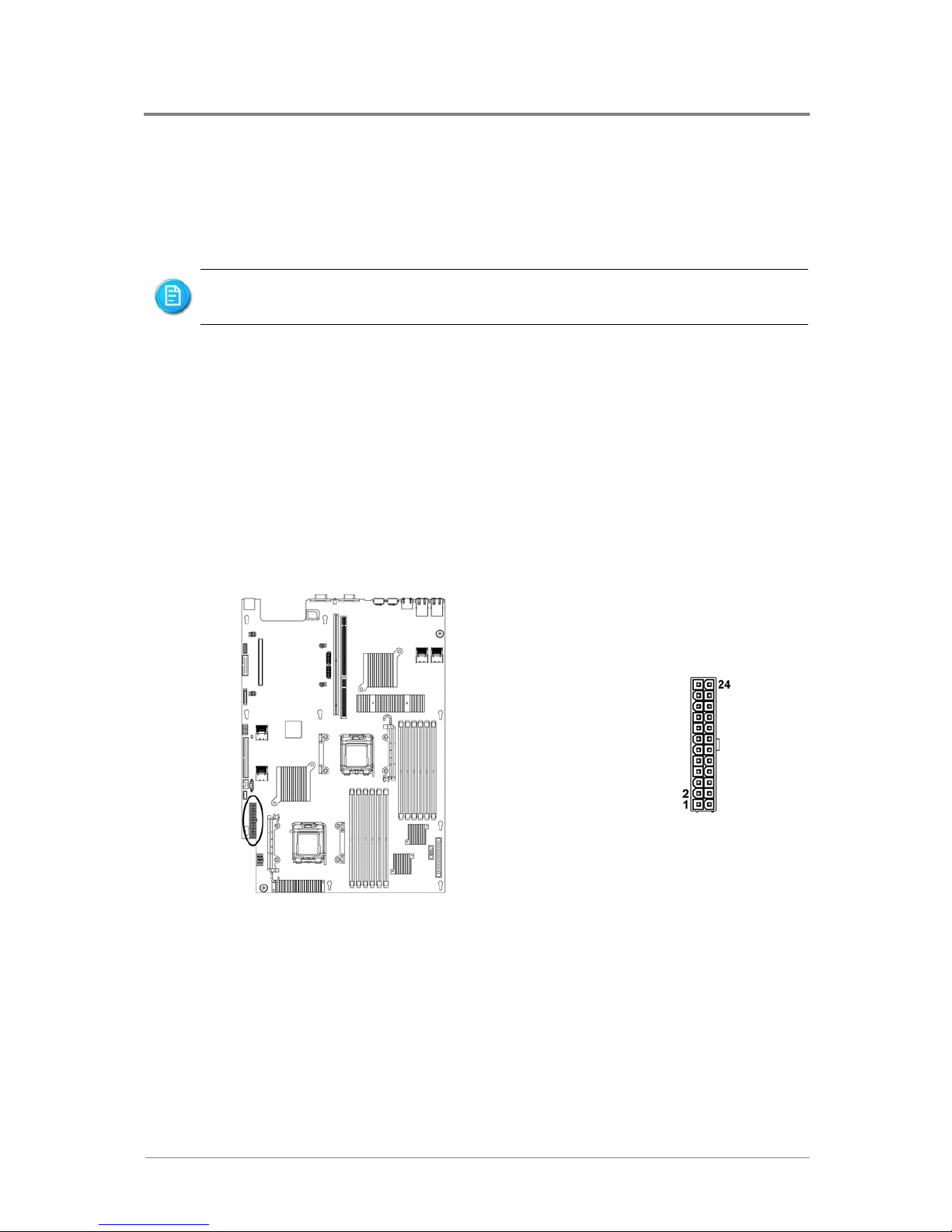
3.1.1 Main Power Connector (J8)
The main power connector and the pin definition are shown below:
Figure 3-1 Main Power Connector
Connectors and Jumper
1230B0026701
3-2
Table 3-1 Main Power Connector Pin Definition
Signal Name Pin Pin Signal Name
+3.3V 1 13 +3.3V
+3.3V 2 14 -12V
Ground 3 15 Ground
+5V 4 16 DC_ON (Sof t On/Off)
Ground 5 17 Ground
+5V 6 18 Ground
Ground 7 19 Ground
Power Good 8 20 NC
Stand By +5V 9 21 +5V
+12V 10 22 +5V
+12V 11 23 +5V
+3.3V 12 24 Ground
3.1.2 Processor Power Connector (J6)
The processor power connector and the pin definition are shown below:
Figure 3-2 Processor Power Connector
Table 3-2 Processor Power Connector Pin Definition
Signal Name Pin Pin Signal Name
Ground 1 5 +12V1
Ground 2 6 +12V1
Ground 3 7 +12V2
Ground 4 8 +12V2
Connectors and Jumper
1230B0026701
3-3
The server will not boot if the 12V processor power connector is not attached to the
motherboard.
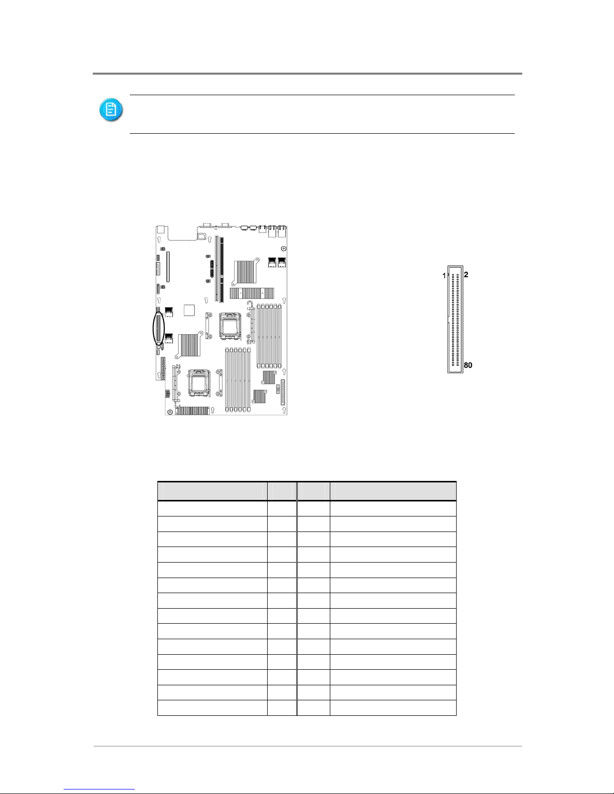
33..22 FFrroonntt PPaanneell IIDDEE CCoonnnneeccttoorr ((JJ2244))
The motherboard provides one 80-pin front panel IDE connector.
The front panel IDE connector and the pin definition are shown below:
Figure 3-3 Front Panel IDE Connector
Table 3-3 Front Panel IDE Connector Pin Definition
Signal Name Pin Pin Signal Name
LED_POWER 1 2 5V_DUAL
Ground 3 4 FAN_FAIL
HD_ACT 5 6 FAN_FAIL_N
HD_ACT_N 7 8 SYS_HEALTH
PWR_BTN_N 9 10 SYS_HEALTH_N
Ground 11 12 NIC1_GRN_N
RST_BTN_N 13 14 NIC1_YEL_N
Ground 15 16 I2C_SDA_BMC
SLP_BTN_N 17 18 I2C_SCL_BMC
Ground 19 20 INTRUDER_N
NMI_BTN_N 21 22 NIC2_GRN_N
UID_LED 23 24 NIC2_YEL_N
Ground 25 26 UID_BTN_N
IDE_RST_N 27 28 Ground

Connectors and Jumper
1230B0026701
3-4
Signal Name Pin Pin Signal Name
IDE_D[7] 29 30 IDE_D[8]
IDE_D[6] 31 32 IDE_D[9]
IDE_D[5] 33 34 IDE_D[10]
IDE_D[4] 35 36 IDE_D[11]
IDE_D[3] 37 38 IDE_D[12]
IDE_D[2] 39 40 IDE_D[13]
IDE_D[1] 41 42 IDE_D[14]
IDE_D[0] 43 44 IDE_D[15]
Ground 45 46 Ground
IDE_DDRFQ 47 48 Ground
IDE_DIOW_N 49 50 IDE_CSEL
IDE_DIOR_N 51 52 Ground
IDE_IORDY 53 54 Ground
IDE_DDACK_N 55 56 IDE_CABLE40_SENSE_N
IDE_IRQ 57 58 Ground
IDE_DA[1] 59 60 IDE_DA[2]
IDE_DA[0] 61 62 IDE_CS1_N
IDE_CS0_N 63 64 IDE_PRSNT_N
Ground 65 66 Ground
SYS_ID[0] 67 68 SYS_ID[1]
SYS_ID[2] 69 70 SYS_ID[3]
I2C_SDA_SB 71 72 I2C_SCL_SB
I2C_ALERT_SB_N 73 74 Ground
SYS_ID[4] 75 76 Ground
+5V 77 78 +5V
5V_DUAL 79 80 +5V
Connectors and Jumper
1230B0026701
3-5
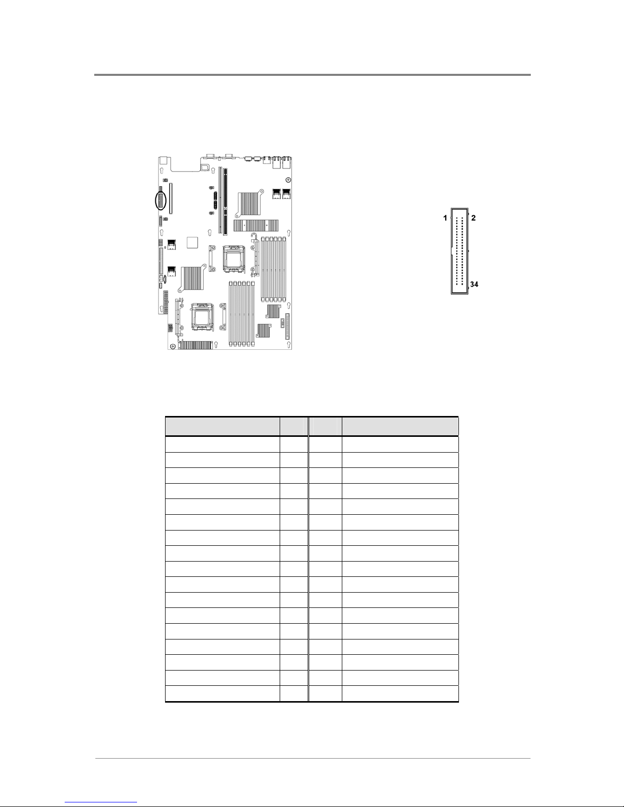
33..33 FFllooppppyy CCoonnnneeccttoorr ((JJ4455))
The 34-pin floppy connector and the pin definition are shown below:
Figure 3-4 Floppy Connector
Table 3-4 Floppy Connector Pin Definition
Signal Name Pin Pin Signal Name
Ground 1 2 LOWDEN_N
Ground 3 4 +5V
KEY 5 6 +5V
Ground 7 8 INDEX_N
Ground 9 10 MOTON0_N
Ground 11 12 +12V
Ground 13 14 DSEL0_N
Ground 15 16 +12V
MSEN 1 17 18 DIR_N
Ground 19 20 STEP_N
Ground 21 22 WDATA_N
Ground 23 24 WRTEN_N
Ground 25 26 TRK_0_N
MSEN 0 27 28 WPROTECT_N
Ground 29 30 RDATA_N
Ground 31 32 HDSEL_N
Ground 33 34 DSKCHING_N

Connectors and Jumper
1230B0026701
3-6
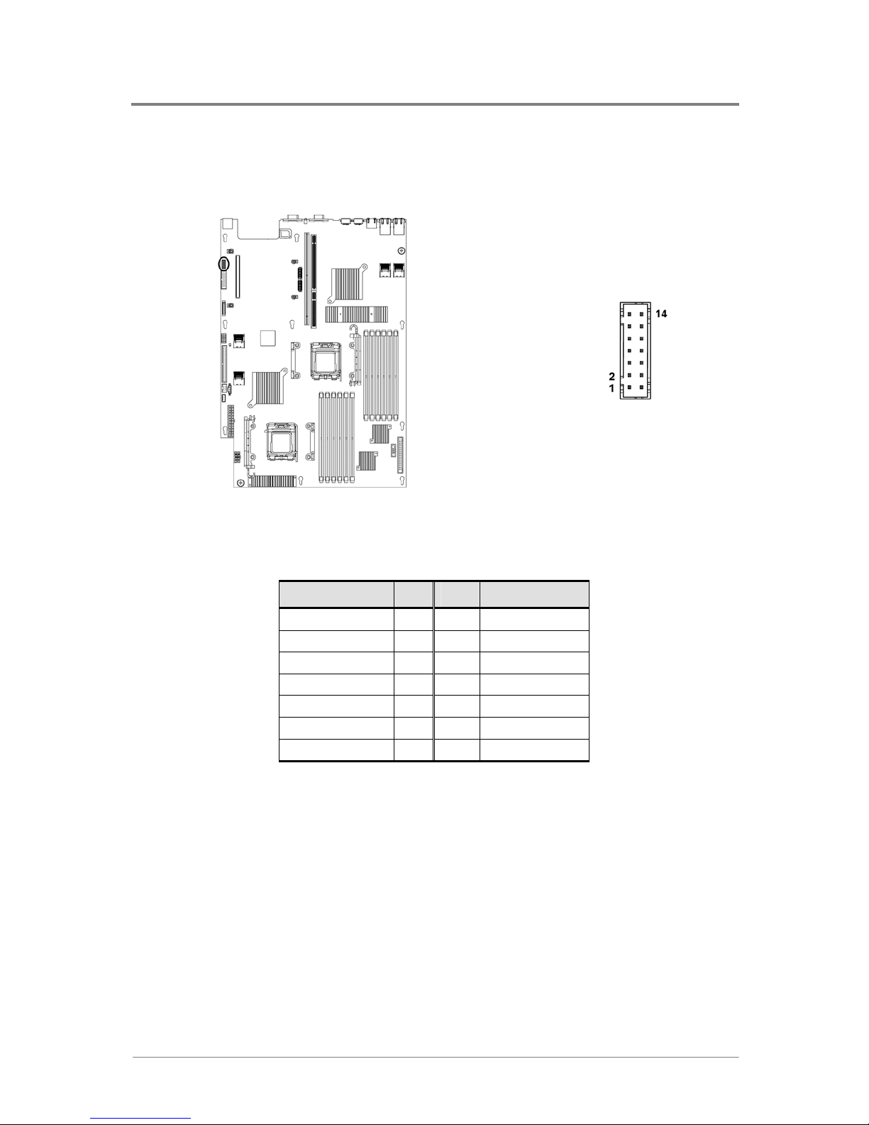
33..44 CChhaassssiiss IInnttrruussiioonn CCoonnnneeccttoorr ((JJ2277))
The 2-pin chassis intrusion connector and the pin definition are shown below:
Figure 3-5 Chassis Intrusion Connector
Table 3-5 Chassis Intrusion Connector Pin Definition
Pin Signal Name
1 Intrusion Signal
2 Ground
Connectors and Jumper
1230B0026701
3-7
33..55 FFrroonntt PPaanneell VVGGAA CCoonnnneeccttoorr ((JJ6688))
The front panel VGA connector and the pin definition are shown below:
Figure 3-6 Front Panel VGA Connector
Table 3-6 Front Panel VGA Connector Pin Definition
Signal Name Pin Pin Signal Name
RED 1 8 Horizontal Sync
Ground 2 9 Ground
GREEN 3 10 Vertical Sync
Ground 4 11 Ground
BLUE 5 12 SCL
Ground 6 13 SDA
Front VGA Use 7 14 Ground
Connectors and Jumper
1230B0026701
3-8
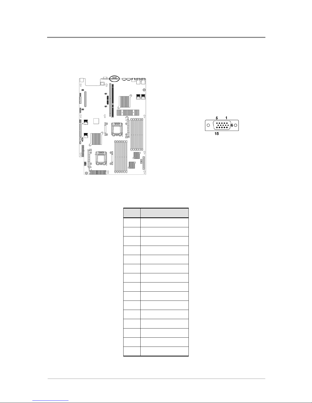
33..66 DD--ssuubb VVGGAA PPoorrtt ((JJ6611))
The 15-pin D-sub VGA port and the pin definition are shown below:
Figure 3-7 D-sub VGA Port
Table 3-7 D-sub VGA Port Pin Definition
Pin Signal Name
1 RED
2 GREEN
3 BLUE
4 NC
5 Ground
6 Ground
7 Ground
8 Ground
9 +5V
10 Ground
11 NC
12 SDA
13 Horizontal Sync
14 Vertical Sync
15 SCL
Connectors and Jumper
1230B0026701
3-9
33..77 SSeerriiaall PPoorrtt ((JJ6622))
The motherboard has one 9-pin serial port connector. The serial port and the pin definition are shown
below:
Figure 3-8 Serial Port
Table 3-8 Serial Port Pin Definition
Pin Signal Name
1 DCD
2 RXDATA
3 TXDATA
4 DTR
5 Ground
6 DSR
7 RTS
8 CTS
9 RI

Connectors and Jumper
1230B0026701
3-10
33..88 KKeeyybbooaarrdd aanndd MMoouussee PPoorrttss ((JJ6600,, JJ5599))
PS/2 keyboard and mouse ports are located on the back panel. The +5 V lines to these ports are protected
with a PolySwitch* circuit that, like a self-healing fuse, reestablishes the connection after an overcurrent
condition is removed.
The PS/2 keyboard port and the pin definitions are shown below:
Figure 3-9 Keyboard Port
Table 3-9 Keyboard Port Pin Definition
Pin Signal Name
1 Keyboard Data
2 NC
3 Ground
4 +5V
5 Keyboard Clock
6 NC

Connectors and Jumper
1230B0026701
3-11
The PS/2 mouse port and the pin definition are shown below:
Figure 3-10 Mouse Port
Table 3-10 Mouse Port Pin Definition
Pin Signal Name
1 Mouse Data
2 NC
3 Ground
4 +5V
5 Mouse Clock
6 NC
The power to the server should be turned off before a keyboard or mouse is connected or disconnected.
The keyboard and mouse controller contains the AMI keyboard and mouse controller code, provides the
keyboard and mouse control functions, and supports password protection for power-on/reset. A
power-on/reset password can be specified in the BIOS Setup program.

Connectors and Jumper
1230B0026701
3-12
33..99 RReeaarr DDuuaall UUSSBB PPoorrtt ((JJ5588))
The motherboard supports rear dual USB port. The rear dual USB port and the pin definition are shown
below:
Figure 3-11 Rear Dual USB Port
Table 3-11 Rear Dual USB Port Pin Definition
Pin Signal Name
1 +5V
2 USB1 Data3 USB1 Data+
4 Ground
5 +5V
6 USB2 Data7 USB2 Data+
8 Ground

Connectors and Jumper
1230B0026701
3-13
33..1100 FFrroonntt PPaanneell UUSSBB CCoonnnneeccttoorr ((JJ1199))
A header on the motherboard provides an option to support one additional 10-pin USB connector.
The front panel USB connector and the pin definition are shown below:
Figure 3-12 Front Panel USB Connector
Table 3-12 Front Panel USB Connector Pin Definition
Signal Name Pin Pin Signal Name
+5V 1 2 +5V
Ground 3 4 Ground
USB0 Data- 5 6 USB1 DataUSB0 Data+ 7 8 USB1 Data+
Ground 9 10 Ground
USB ports may be assigned as needed.

Connectors and Jumper
1230B0026701
3-14
33..1111 I
I
2
2
CC ((SSMMBBuuss)) SSiiggnnaall CCoonnnneeccttoorr ffoorr PPSSUU ((JJ2200))
The 5-pin I2C (SMBus) signal connector for PSU and the pin definition are shown below:
Figure 3-13 I
2
C (SMBus) Signal Connector for PSU
Table 3-13 I
2
C (SMBus) Signal Connector for PSU Pin Definition
Pin Signal Name
1 I2C SCL
2 I2C SDA
3 I2C Alert
4 Ground
5 +3.3V

Connectors and Jumper
1230B0026701
3-15
33..1122 TTwwoo DDuuaall NNIICC CCoonnnneeccttoorrss ((RRJJ4455)) ((JJ5566,, JJ5577))
The motherboard supports two dual NIC connectors (RJ45). The dual NIC connector is shown below:
Figure 3-14 Dual NIC Connector (RJ45)
Table 3-14 Dual NIC Connector (RJ45) Pin Definition
Pin Signal Name
1 NIC_CHA_TRX0_DN
2 NIC_CHA_TRX0_DP
3 NIC_CHA_TRX1_DN
4 NIC_CHA_TRX1_DP
5 NIC_CHA_TRX2_DN
6 NIC_CHA_TRX2_DP
7 NIC_CHA_TRX3_DN
8 NIC_CHA_TRX3_DP
9 P1V8_DUAL
10 Ground
11 NIC_CHB_TRX0_DN
12 NIC_CHB_TRX0_DP
13 NIC_CHB_TRX1_DN
14 NIC_CHB_TRX1_DP
15 NIC_CHB_TRX2_DN
16 NIC_CHB_TRX2_DP

Connectors and Jumper
1230B0026701
3-16
17 NIC_CHB_TRX3_DN
18 NIC_CHB_TRX3_DP
19 P1V8_DUAL
20 Ground
21 NIC0_LED0_N
22 P3V3_DUAL
23 P3V3_DUAL
24 NIC0_LED1_N
25 NIC1_LED0_N
26 P3V3_DUAL
27 P3V3_DUAL
28 NIC1_LED1_N
29 Ground
30 Ground
31 Ground
32 Ground
Dual NIC connector (J56) is used for 2U server.
Connectors and Jumper
1230B0026701
3-17
33..1133 MMaannaaggeemmeenntt PPoorrtt ((RRJJ4455)) ((JJ7755))
The motherboard supports one management port (RJ45). The connector is shown below:
Figure 3-15 Management Port (RJ45)
Table 3-15 Management Port (RJ45) Pin Definition
Pin Signal Name
1 Ethernet 10/100 Transmit+
2 Ethernet 10/100 Transmit3 Ethernet 10/100 Receive+
4 Unused
5 Unused
6 Ethernet 10/100 Receive7 Unused
8 Unused
9 N/A
10 N/A
11 Ground
12 Ground
13 SPEED LED+
14 SPEED LED15 LINKUP/ACTIVITY LED+
16 LINKUP/ACTIVITY LED-

Connectors and Jumper
1230B0026701
3-18
33..1144 FFaann BBooaarrdd CCoonnnneeccttoorr ((JJ11))
The fan board connector and the pin definition are shown below:
Figure 3-16 Fan Board Connector
Table 3-16 Fan Board Connector Pin Definition
Signal Name Pin Pin Signal Name
BMC_FAN_TACH_SEL0 1 2 BMC_FAN_TACH_SEL1
FAN_BMC_TACH1 3 4
FAN_BMC_TACH2
FAN_BMC_TACH3
5 6
FAN_BMC_TACH4
FAN_BMC_TACH5
7 8
FAN_BMC_TACH6
FAN_BMC_TACH7
9 10
FAN_BMC_TACH8
FAN_CNTR_PWM1 11 12 FAN_CNTR_PWM2
I2C_SCL_FAN_CNTR_R 13 14 I2C_SDA_FAN_CNTR_R
5V_DUAL 15 16 +3.3V
+12V 17 18 I2C_ALERT_FAN_N
+12V 19 20 +12V
+12V 21 22 +12V
+12V 23 24 +12V
+12V 25 26
+12V
+12V 27 28
+12V
+12V 29 30 Ground
Ground
31 32
Ground
Connectors and Jumper
1230B0026701
3-19
Signal Name Pin Pin Signal Name
Ground
33 34
Ground
Ground
35 36
Ground
Ground
37 38
Ground
Ground
39 40
Ground
33..1155 MMiinnii--SSAASS CCoonnnneeccttoorrss ((JJ6699,, JJ7700,, JJ7711,, JJ7722))
The Mini-SAS connector is shown below:
Figure 3-17 Mini-SAS Connector
Table 3-17 Mini-SAS Connector Pin Definition
Signal Name Pin Pin Signal Name
Ground B1 A1 Ground
SATA_TX1_C_DP B2 A2 SATA_RX1_C_DP
SATA_TX1_C_DN B3 A3 SATA_RX1_C_DN
Ground B4 A4 Ground
SATA_TX2_C_DP B5 A5 SATA_RX2_C_DP
SATA_TX2_C_DN B6 A6 SATA_RX2_C_DN
Ground B7 A7 Ground
SB_SATA_SCLK B8 A8 Key
SB_SATA_SLOAD B9 A9 Ground
Ground B10 A10 SB_SATA_SDO0
Ground B11 A11 SB_SATA_SDO1

Connectors and Jumper
1230B0026701
3-20
Signal Name Pin Pin Signal Name
Ground B12 A12 Ground
SATA_TX3_C_DP B13 A13 SATA_RX3_C_DP
SATA_TX3_C_DN B14 A14 SATA_RX3_C_DN
Ground B15 A15 Ground
SATA_TX4_C_DP B16 A16 SATA_RX4_C_DP
SATA_TX4_C_DN B17 A17 SATA_RX4_C_DN
Ground B18 A18 Ground
Mini-SAS connectors (J71, J72) are used for 2U server.
33..1166 LLCCMM CCoonnnneeccttoorr ((OOppttiioonnaall)) ((JJ7733))
The LCM connector and the pin definition are shown below:
Figure 3-18 LCM Connector
Table 3-18 LCM Connector Pin Definition
Signal Name Pin Pin Signal Name
5V_DUAL 1 2 5V_DUAL
I2C_SDA_LCM 3 4 I2C_SCL_LCM
Ground 5 6 Ground
NC 7 8 NC
NC 9 10 Key
Connectors and Jumper
1230B0026701
3-21
33..1177 IInntteerrnnaall UUSSBB PPoorrtt ffoorr UUSSBB FFllooppppyy ((JJ6677))
The internal USB port for USB floppy and the pin definition are shown below:
Figure 3-19 Internal USB Port for USB Floppy
Table 3-19 Internal USB Port for USB Floppy Pin Definition
Pin Signal Name
1 +5V
2 USB5 Data3 USB5 Data+
4 Ground
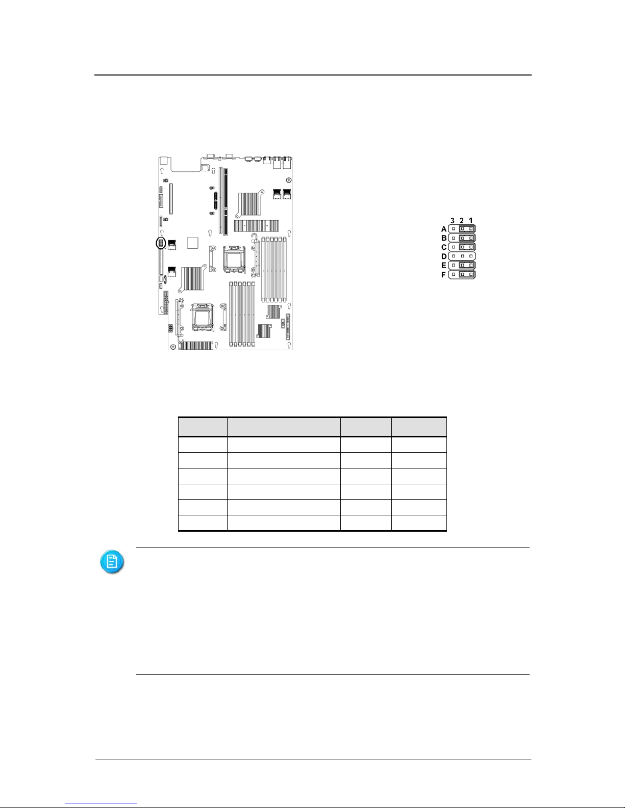
Connectors and Jumper
1230B0026701
3-22
33..1188 SSyysstteemm CCoonnffiigguurraattiioonn JJuummppeerr SSeettttiinngg ((JJ5544))
The function of system configuration jumper installed on motherboard is shown below:
Figure 3-20 System Configuration Jumper
Table 3-20 System Configuration Jumper Function
Jumper Function Pin 1-2 Pin 2-3
A Clear Password *Disable Enable
B
Clear CMOS *Disable Enable
C
BIOS Boot Block Protect *Enable Disable
D
Reserved ─ ─
E
BIOS Recovery *Disable Enable
F
BMC Recovery *Disable Enable
The “*” in the table of system configuration jumper describes the default status.
The “Clear CMOS” procedure is shown as below:
(a). Sets the “Clear CMOS” jumper to enable.
(b). BIOS detects the jumper settings changed and clear CMOS-data without the time and
date information during POST.
(c). The Jumper-J54-B (Clear CMOS) is taken off and set on, please set to “Disable”.
(d). Turn DC power off and set jumpers to disable.

Chapter 4
BIOS Setup
BIOS Setup Utility
Entering the BIOS Setup Utility
Keyboard Command Bar
BIOS Updates

BIOS Setup
1230B0026701
4-1
44 BBIIOOSS SSeettuupp
This section describes the BIOS Setup Utility options. You can run BIOS Setup with or without an
operating system being present. Onboard devices are configured with the BIOS Setup utility that is
embedded in flash ROM.
The configuration utilities allow you to modify the CMOS RAM and NVRAM. The actual hardware
configuration is accomplished by the BIOS POST routines and the BIOS Plug-N-Play auto-configuration
manager. The configuration utilities update a checksum for both areas, so potential data corruption is
detected by the BIOS before the hardware configuration is saved. If the data is corrupted, the BIOS
requests that the user reconfigure the system and reboot.
Because the BIOS code is the most often changed part of the motherboard design, the
BIOS information described in this section may be a little different compared to the actual
BIOS that contained in your motherboard.
44..11 BBIIOOSS SSeettuupp UUttiilliittyy
This section describes the ROM-resident setup utility that provides the means to configure the platform.
The BIOS Setup utility is part of the system BIOS and allows limited control over onboard resources.
The user can disable embedded PCI devices through the setup menus. When these devices are disabled
through setup, their resources are freed.
The following embedded devices can be disabled through setup menus, making them invisible to a
plug-and-play operating system that scans the PCI bus:
Network controllers embedded in nVIDIA MCP55Pro and IO 55 (For 2U)
Onboard VGA embedded in Pilot SMC
BIOS Setup
1230B0026701
4-2
The BIOS options described in this section may or may not be present in pre-production
versions of the system BIOS. This section describes the BIOS utility as it is planned to be
at production and is subject to change. Option locations, in a given menu of the BIOS
Setup utility as described in this section, may be different from those observed on any one
pre-production version of the system BIOS.
The BIOS Setup utility screen is divided into four functional areas.
Table 4-1 BIOS Setup Utility Screen Description
Functional Area Description
Keyboard
Command Bar
Located at the bottom of the right screen or as part of
the help screen. This bar displays the keyboard
commands supported by the setup utility
Menu Selection Bar
Located at the top of the screen. Displays the various
major menu selections available to the user. The
Server Setup utility major menus are: Main Menu,
Advanced Menu, Boot Menu, Security Menu and Exit
Menu
Options Menu
Each Option Menu occupies the left and center
sections of the screen. Each menu contains a set of
features. Selecting certain features within a major
Option Menu drops you into sub-menus
Item Specific Help
Screen
An item-specific Help screen is located at the upside
of the right side of the screen
44..22 EEnntteerriinngg tthhee BBIIOOSS SSeettuupp UUttiilliittyy
During the BIOS POST operation, the user is prompted to use the Del function key to enter Setup as
follows:
Press Del to run SETUP.
Press Tab to enter Diagnostic Messages. Then, press F11 again to enter BBS POPUP.
A few seconds might pass before Setup is entered. This is the result of POST completing test and
initialization functions that must be completed before Setup can be entered. When Setup is entered, the
Main Menu options page is displayed.

BIOS Setup
1230B0026701
4-3
44..33 KKeeyybbooaarrdd CCoommmmaanndd BBaarr
The right portion of the Setup screen provides a list of commands that are used to navigate through the
Setup utility. These commands are displayed at all times.
Each menu page contains a number of configurable options and/or informational fields. Depending on
the level of security in affect, configurable options may or may not be changed. If an option cannot be
changed due to the security level, its selection field is made inaccessible.
The Keyboard Command Bar supports the following:
Table 4-2 Keyboard Command Bar Description
Key Option Description
Enter Execute
Command
The Enter key is used to activate sub-menus when the selected feature
is a sub-menu, or to display a pick list if a selected option has a value
field, or to select a sub-field for multi-valued features like time and
date. If a pick list is displayed, the Enter key will undo the pick list,
and allow another selection in the parent menu.
ESC Exit The ESC key provides a mechanism for backing out of any field. This
key will undo the pressing of the Enter key. When the ESC key is
pressed while editing any field or selecting features of a menu, the
parent menu is re-entered.
When the ESC key is pressed in any sub-menu, the parent menu is
re-entered. When the ESC key is pressed in any major menu, the exit
confirmation window is displayed and the user is asked whether
changes can be discarded. If “No” is selected and the Enter key is
pressed, or if the ESC key i s p ress e d, the user is returned to where
they were before ESC was pressed without affecting any existing
settings. If “Yes” is selected and the Enter key is pressed, Setup is
exited and the BIOS continues with POST.
↑
Select Item The up arrow is used to select the previous value in a pick list, or the
previous options in a menu item's option list. The selected item must
then be activated by pressing the Enter key.
↓
Select Item The down arrow is used to select the next value in a menu item’s
option list, or a value field’s pick list. The selected item must then be
activated by pressing the Enter key.
← →
Select
Menu
The left and right arrow keys are used to move between the major
menu pages. The keys have no affect if a sub-menu or pick list is
displayed.

BIOS Setup
1230B0026701
4-4
Key Option Description
T a b Select Field The T a b key is used to move between fields . For example , T ab can be
used to move from hours to minutes in the time item in the main
menu.
- Change
Value
The minus key on the keypad is used to change the value of the
current item to the previous value. This key scrolls through the values
in the associated pick list without displaying the full list.
+ Change
Value
The plus key on the keypad is used to change the value of the current
menu item to the next value. This key scrolls through the values in the
associated pick list without displaying the full list. On 106-key
Japanese keyboa r ds, t he p lus ke y ha s a different scan code than the
plus key on the other keyboard, but will have the same effect
F9 Load
Optimal
Defaults
Pressing F9 causes the following to appear:
Setup Confirmation
Load Optimal Defaults?
[OK] [Cancel]
If “OK” is selected and the Enter key is pressed, all Setup fields are
set to their default values. If “Cancel” is selected and the Enter key is
pressed, or if the ESC key i s p ress e d, the user is returned to where
they were before F9 was pressed without affecting any existing field
values.
F10 Save and
Exit
Pressing F10 causes the following message to appear:
Setup Confirmation
Save Configuration changes and exit setup?
[OK] [Cancel]
If “OK” is selected and the Enter key is pressed, all changes are saved
and Setup is exited. If “Cancel” is selected and the Enter key is
pressed, or the ESC key is pressed, the user is returned to where they
were before F10 was pressed without affecting any existing values.

BIOS Setup
1230B0026701
4-5
44..44 BBIIOOSS UUppddaatteess
4.4.1 BIOS Requirements
Table 4-3 BIOS Requirements Description
U
tilities
F
ile Name
D
escription
Flash BIOS Image
Under DOS
AFUDOS.EXE
ROM image file
FBB.BAT
AMIBIOS Flash Utility &
ROM image
Flash BIOS Image
Under Windows PE
AFUWIN.EXE
ROM image file
FBB.BAT
AMIBIOS Flash Utility
ROM image
Recovery Mode AMIBOOT.ROM ROM image
4.4.2 ROM Flash
Update under DOS prompt
• Copy AFUDOS.EXE, FBB.BAT and RomFileName.rom (ROM image) to bootable storage.
• Plug the bootable storage (ex: USB or Floppy disk) and boot to DOS prompt (no HIMEM).
• Run FBB.BAT (depend on if Boot Block is needed to be updated).
FBB.BAT 1: Updates system ROM only, but Boot Block does not change.
FBB.BAT 2: Updates both system ROM and Boot Block.
• Restart sy stem & load BIOS default value.
Recovery Mode
• Prepare USB disk on key (or Floppy disk/CD-ROM) for recovery.
1) Format USB Disk on Key (or Floppy disk/CD-ROM) with FAT16/FAT32 format.
2) Copy ROM image and rename it to AMIBOOT.ROM.
• Recovery method:
1) Turn on the Recovery Ju mper J54-E or the hot key “Ctrl” + “Home” to invoke recovery function
during POST.
2) Plug USB Disk on Key (or Floppy/CD-ROM).
3) Power on computer wait for recovery process complete.
4) Unplug USB Disk on Key (or Floppy/CD-ROM) & Turn off the Recovery Jumper.
5) Restart computer & load BIOS default.
 Loading...