

Peak 632A User Manual

PEAK 632A
Single Board Computer
User
′′′′
s Manual
All brand names are registered trademarks of their respective owners.

Copyright 2000
All rights reserved
Edition 1.0 July, 2000
The information in this document is subj ect to change w ithout prior notice in order to im prove
reliability, design and function. The information in this docum ent does not represent
commitm ent on the part of the m anufacturer.
In no event will the manufacturer be liable for direct, indirect, special, incidental, or
consequential damages arising out of the use of the PEA K 632A , nor for any infringements upon
the rights of third parties which may result from such use.
This document contains proprietary inform ation protected by copyright. All rights are reserved.
No part of this manual m ay be reproduced by any mechanical, electronic, or other means in any
form without prior written per mission of the m anufacturer.
Trademarks
PEAK 632A is a registered trademark of NEX COM International Co., Ltd.
IBM PC is a registered trademark of International Business Machines Corporation.
Intel and Pentium are registered trademarks of Intel Corporation. Award is a registered
trademark of Award Software, Inc.
Other product names m entioned herein are used for identification purposes only and may be
trademarks and/or registered trademarks of their respective com panies.

Table of Contents
How to Use This Guide
Chapter 1 Introduction
1.1 Intro d uction.................................. ................... .................... ..-1
1.2 Features
……..
….1-1
1.3 Specifications
.1-2
1.4 Packing List
..
1-6
Chapter 2 Switche s and Connectors
2.1 Switches........................................... ..... ......
..........................2-1
2.2 Connectors...................................................................................2-4
Chapter 3 System Memory and CPU Installation
3.1 System Memory.......................................................................3-1
3.2 Cache Memory ........................................................................3-3
3.3 Chang CPU..................................................................
3-
Chapter 4 Award BIOS Setup
4.1 Entering Setup.........................................................................4-1
4.2 Control Keys .....................
........................................... 4-2
4.3 Getting Help ............................…................................................ 4-3
4.4 The Main Menu ........................................................................... 4-4
4.5 Standard CMOS Setup ............................................................ 4-7
4.6 BIOS Features Setup. ..................…...........................................-11
4.7 Chipset Features Setup............................................................…4-16
4.8 Power Management Setup...........................................................4-20
4.9 PnP/PCI Configuration..........................................................….4-25

4.10 IDE HDD Auto Detection ......................................................... 4-31
4.11 Supervisor/User Password Setting.............................
….......4-35
4.12 IDE HDD Auto Detection
........................................4-36
4.13Power-On Boot
…...
.......................-41
4.14 BIOS Reference – POST messages
4-42
4.15 BIOS Default Drive Table
….
….
….….4-48
Chapter 5 VG A Driver Installation Procedures
5.1 Windows 95/98 Drivers S etup Procedure
…
…..5-1
5.2 Windows NT Drivers Setup Procedure
.. 5-12
Chapter 6 LAN Driver Installation Procedures
6.1 Windows 95/98 Drivers Setup Procedure
..…6-1
6.2 Windows NT Drivers Setup Procedure
...….… 6-6
Chapter 7 SCSI D river Installation Procedures
6.1 Windows 95/98 Drivers Setup Procedure
..…6-1
6.2 Windows NT Drivers Setup Procedure
...
7-11
Appendix A Watchdog Timer
Appendix B Memory Mapping

How to use this manual
This manual is writte n to help you use the PCA-6551V E. It describes how to m ake various
settings on the Pentium
®
CPU board to m eet your requirem ents. A brief sum mary of the manual
follows:
Chapter 1
“Introductiongives an overview of the product specifications. It also tells you
what is included in the product package.
Chapter 2
umpers and Connectorsdescribes the definitions and positions of jumpers and
connectors that you may easily configure and set up according to y our particular requirem ents.
Chapter 3
ystem Expansiondescribes how to change or expand the CPU board by changing
the system m emory, cache mem ory, and/or CPU. These changes will y ield more power from the
CPU board.
Chapter 4
ward BIOS Setupdescribes how to use the advanced PCI/Green BIOS to control
almost every feature of the PCA-6551VE, including the w atchdog tim er.
Chapter 5
“VGA Driver Installation Procedures” gives instructions for installing and operating
the software drivers on the utility disk included in your package.
Chapter 6
“LAN Driver Installation Procedures” provides detailed information on Ethernet
configura tion, and shows how to change the configuration to match your application
requirements.
Chapter 7
“SCSI Driver Installation Procedures” provides detailed inform ation for installing
and operating the software drivers, and shows how to change the configura tion to match your
application requirements.
Appendix A
“Watchdog Timer”describes how to set up the watchdog tim er (WDT), and gives
an example of programm ing the W DT .
Appendix B
“Memory Mapping” describes usage of the 1st MB memory.

Peak 632A User's Guide
Specifications
1-1
Chapter 1
1-1 Introduction
The PEAK 632A is a full size Sing l e Bo a r d Comput e r . It applies Single Soc k e t 370
FC-PGA based processor, supporting both 66 MHz (Celeron) and 100 MHz (Pentium
III) Front Side Bus. The memory it can accommodate is 1 GB SDRAM up to 100
MHz.
Meanwhile, this card is on-board with the following three significant I/Os which help
to spare out more PCI slots for other add-on I/Os, i.e. the C&T 69000/69030
VGA/Panel controller through AGP interface; the Intel 82559 Ethernet and the
Adaptec 7890 Ultra 2 SCSI. Components with all o f the abo v e branded and
powerful. PEAK 632A is obv i ously a form i da bl e pla t f o r m ideal for heavy duty and
computer telephony application.
The other on-board I/Os includes 2S1P, the high precision RTC with battery, the
Watch Dog Timer, DOC, IDE×2, FDC×1, USB×2, and PS/2 Keyboard/Mouse.
1-2 Features
!
Intel Celeron/Pentium III CPU with 66/100MHz FSB up to 850 MHz
!
1 GB SDRAM (Max.) memory support, DIMM×4
!
Intel 440BX AGP set
!
C&T 69000 AGP mode VGA controller with CRT/LCD support
!
Intel 82559 10/100 Base Ethernet controll er
!
Adaptec 7890 U2 SCSI controller
!
On board socket for DiskOnChip up to 288MB
!
RS232×2 with 16C550 UARTs, optional RS422/485×1
!
Enhanced parallel port, support SPP/EPP/ECP
!
IDE×2, FDC×1, PS/2 keyboa rd/mouse
!
USB port×2
!
Watchdog Timer
!
ISAMAX support up to 20 slots ISA card

Peak 632A User's Guide
Specifications
1-2
1-3 Specifications
!
System Architecture
!
Full size SBC with PCI/ISA Golden finger
!
Intel Socket 370 Celeron/Pentium III with 66/100MHz FSB
!
PCI V2.1 complied
!
PICMG 1.0 (Rev.2.0) complied
!
CPU Support
!
Intel Celeron/Pentium III CPU with 128/256K cache on die
!
Brand New Sock e t 370 FC - PGA CPU running at 66/100MHz FSB up t o 850MHz
!
Support strea m i ng SIMD instructio n
!
Main Memory
!
Support SDRAM up to 1GB ( M a x.)
!
168 pin DIMM socket×4
!
ECC support (single bit error correction/Multiple bit errors reporting)
!
BIOS
!
Award System BIOS
!
Plug & Play support
!
Advanced Powe r Manag em e nt suppo rt
!
Advanced configuration & Power Interface support
!
2M bit flash ROM
!
Chip Set
!
Intel 82440BX AGP set
!
66/100MHz FSB support
!
PCI V2.1 complied
!
Optimized SDRAM suppo rt
!
On Board VGA
!
C&T 69000 AGP mode VGA contr o l l e r
!
TFT LCD/DSTN LCD/CRT cont r o l

Peak 632A User's Guide
Specifications
1-3
!
2MB SDRAM on die
Maximum Res.
Color & Refresh
Rate
Resolution
Colors Refresh Rate (Hz)
1280×1024
256 60
1024×768
16bits (High color ) 85, 75, 65
800×600
24bits (True color) 85, 75, 65
!
Driver supportWindows 95/98, Windows NT4.0
!
15 pin CRT connector×1, 50 pin LCD pane l connector×1
!
On Board LAN
!
Intel 82559 Single Ethernet controller
!
10 Base T/100 Base TX support, full duplex
!
Complied wi t h PCI V2.1, IEEE802.3, IEEE 802.3U
!
Backward compatible with former 82558 Ethernet controller base net modules
!
Driver support: DOS/Windows , Windo w s 95/98, Windo w s NT4.0, Netware, SCO
Open Server 5.0
!
RJ45 connector×1
!
On Board SCSI
!
Adaptec AIC 7890 RISC SCSI c o nt r o l l e r
!
Brand New Ultra 2 SCSI support
!
80MB/s (Max.) transfer rate, up to 12 meter cable
!
Backward compatible with Ultra Wide SCSI, SCSI II, etc.
!
Driver support: Windows 95/98, Windo w s NT4.0, SCO Ope n Serv e r 5.0
!
68 pin SCSI connector×1
!
On Board I/O
!
Winbond W83977 Super I/O on board
!
SIO×2, with 2×16C550 UARTs, 9 pin D-type×1, 10 pin HEADER×1, optional
RS422/485×1
!
PIO×1, Bi-directional, EPP/ECP support, 26 pin×1
!
Floppy Disk controller: 5.25″360K/1.2MB, 3.5
″

Peak 632A User's Guide
Specifications
1-4
720K/1.2MB/1.44MB/2.88MB support , 34 pi n c o nne c t or×1
!
On chip enhanced IDE×2, PIO up to mode 4, DMA master up to mode 2,
Ultra DMA/33 support, 40 pin×2, total 4 E.IDE Devices support
!
On chip keyboard, mouse controller, PS/2 KeyboardMouse, 5 pin header
×
1, 6 pin mini DIN×2, (for Peak632V/Peak632)PS/2 Keyboard, 6 pin
mini DIN×1, share with PS/2 mouse by Y cable
(for Peak632A/Peak632VL)
!
On board USB port×2 (6 pin header×1)
!
On board buzzer×1
!
On board 2 pin header for reset SW, 4 pin for speaker, 5 pin for keylock
!
On board 3 pin header for +5VSTBY, GND, Pow e r ON#
!
On board 2 pin header for I2C
!
On board reserved CAN Bus connector
!
On Board RTC
"
High precision real time clock/calendar with b attery back up
!
On Board Solid State Disk Socket
!
On board reserved socket for DOC of M-systems2MB~144MB, etc
!
System Monitor
!
Winbond W83782D system monitor controller
!
Six voltage (For +3.3V, +5V, +12V,−12V, Vtt and Vcore )
!
One Fan speed (For CPU)
!
Two temperature
!
Drivers support: Windows 95/98, Windo ws NT4.0
!
ISAMAX Support
!
MaximizeISA signals to support ISA cards up to 20
!
Watchdog Timer
!
1,2,44 seconds time-out intervals
!
Dimensions
!
340mm(D)×122mm(W)
!
Power Requirements
!
+5V20A (Max.)

Peak 632A User's Guide
Specifications
1-5
!
+12V: 500mA (Max.)
!
-12V: 50mA (Max.)
!
Environments
!
Operating temperatures0°C to 60°C
!
Storage temperatures-20°C to 80°C
!
Relative humidity10% to 90% (Non-condensing)
!
Certification
!
CE approval
!
FCC Class A
!
Model Available
!
PEAK 632A--Full-size Socket 370 Celeron/Pentium III AIO CPU Card
!
PEAK 632VL-- Full-size Socket 370 Celeron/Pentium III CPU Card
w/VGA/LAN
!
PEAK 632V--Full-size Socket 370 Celeron/Pentium III CPU Card w/
VGA
!
PEAK 632-- Full-size Socket 370 Celeron/Pentium III CPU Card

Peak 632A User's Guide
Specifications
1-6
1-4 What you'll have from the package
In addition to this manual, the PEAK 632A series package includes the follow ing items.
ITEM
Model
Peak 632A Peak 632VL Peak 632V Peak 632
Peak 632A series
CPU card
1111
IDE cable 1 1 1 1
FDC cable 1 1 1 1
Serial & Printer port
cable
1111
5 pin to 5 pin
keyboard cable
1111
Y cable for
keyboard & mouse
11
××
UW SCSI cable 1
×××
C&T 69000 VGA
driver disks
111
×
Intel 82559
Ethernet driver
disks
22
××
Adaptec 7890
driver disks
3
×××
Winbond W83782D
driver disks
3333
If any of these items is missed or damaged, please contact y our vendor for what y ou
want.
Chapter 2
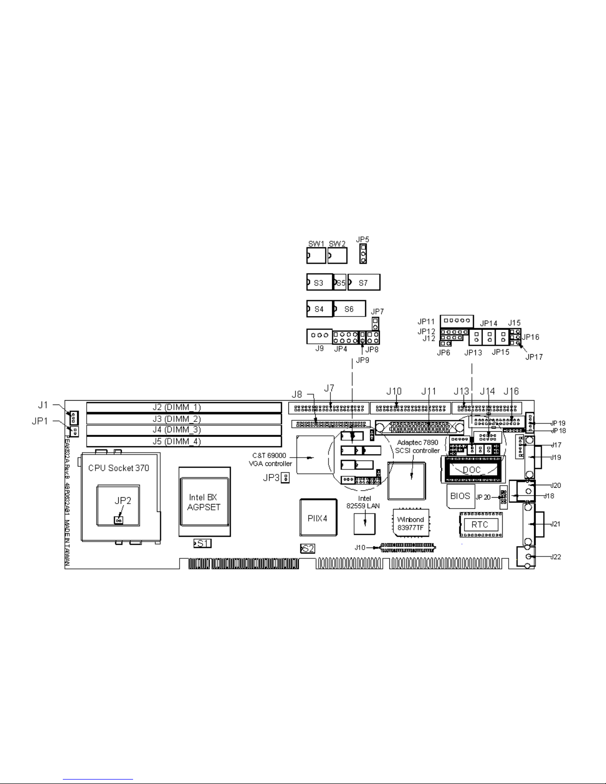
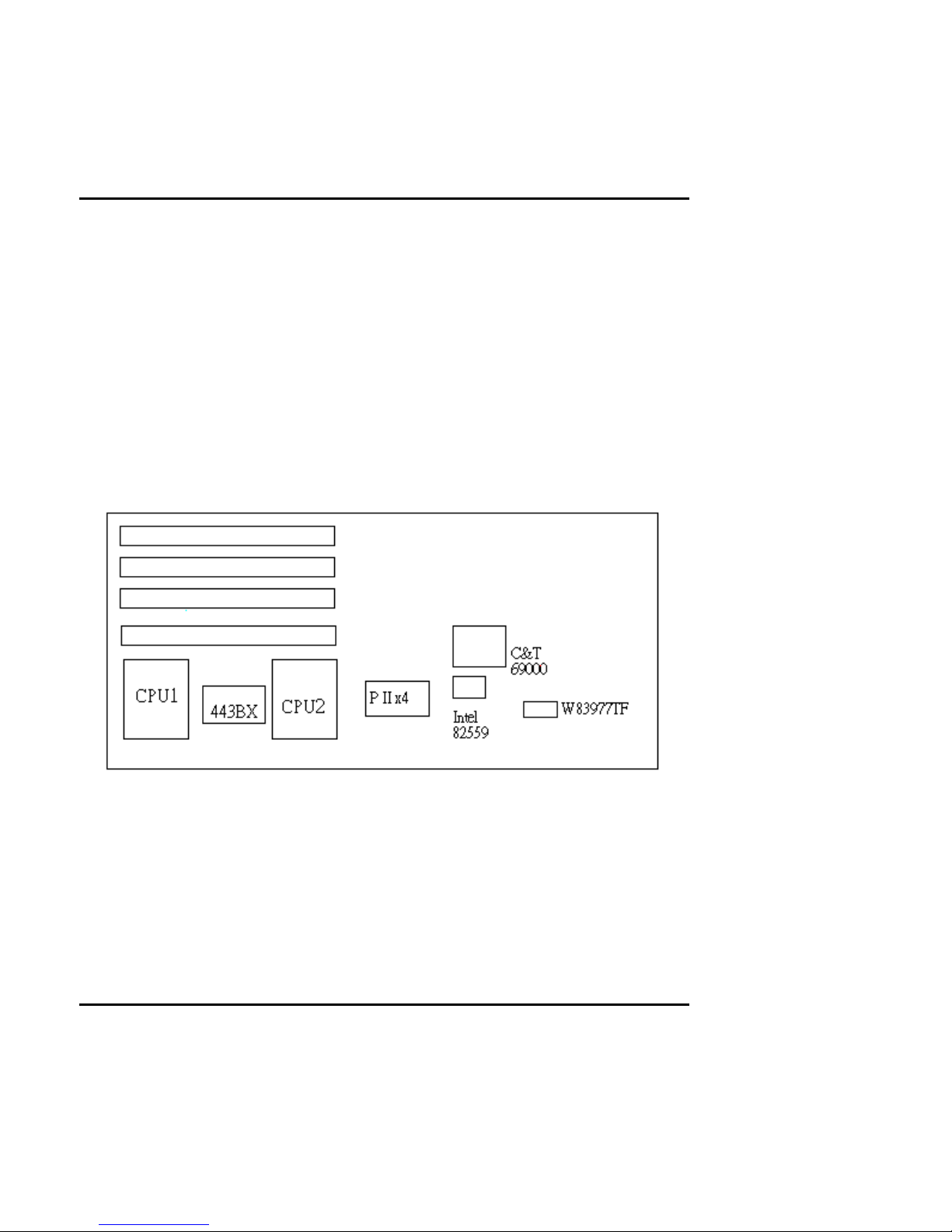
Figure 2-1 Switches and Connectors position
Peak 632A Us er's Guide
Switches and Connectors
2-1
This chapter gives the definitions and shows where to locate the positions of
switches and connectors.
2-1 Switches
Switches on the CPU board are used to select options for different functions used.
The switch-on or off is to accommodate the variations of the following table.
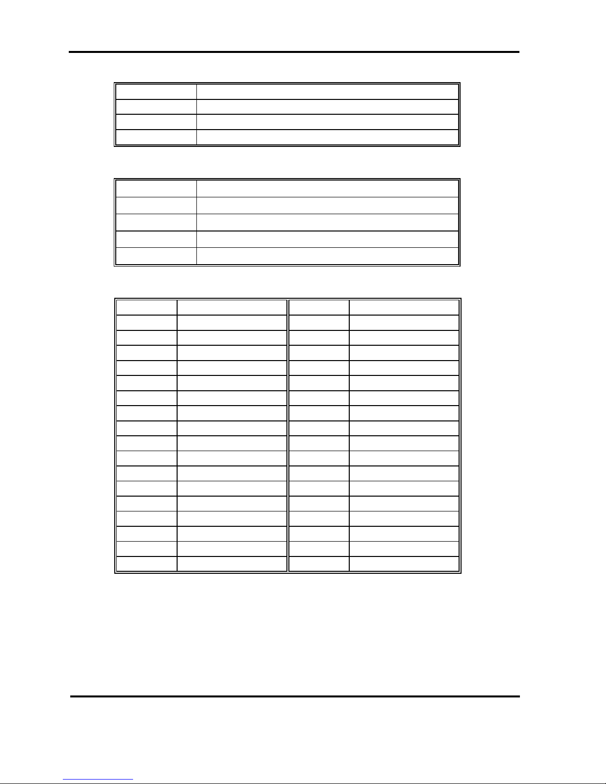
Switch Setting Table (*: default setup)
AT/ATX FUNCTION SELECT
*AT Function ATX Function
JP4 1-2,3-4 5-6,7-8
JP7 N/C 1-2
JP8 1-2 3-4
CPU Frequency
S1.1 S1.2 S1.3 S1.4 S1.5 S1.6 S1.7
*100 OFF OFF ON OFF OFF OFF OFF
66 ON ON ON OFF OFF ON OFF
CPU Pipelined
S1.8
*Enabled OFF
Disabled ON
DEVICE SELECT
S2.1 S2.2 S2.3 S2.4 S2.5 S2.6
*VGA Enabled ON OFF X X X X
VGA Disabled OFF ON X X X X
*SCSI Enabled X X ON OFF X X
SCSI Disabled X X OFF ON X X
*LAN Enabled X X X X ON OFF
LAN Disabled X X X X OFF ON
Peak 632A Us er's Guide
Switches and Connectors
2-2
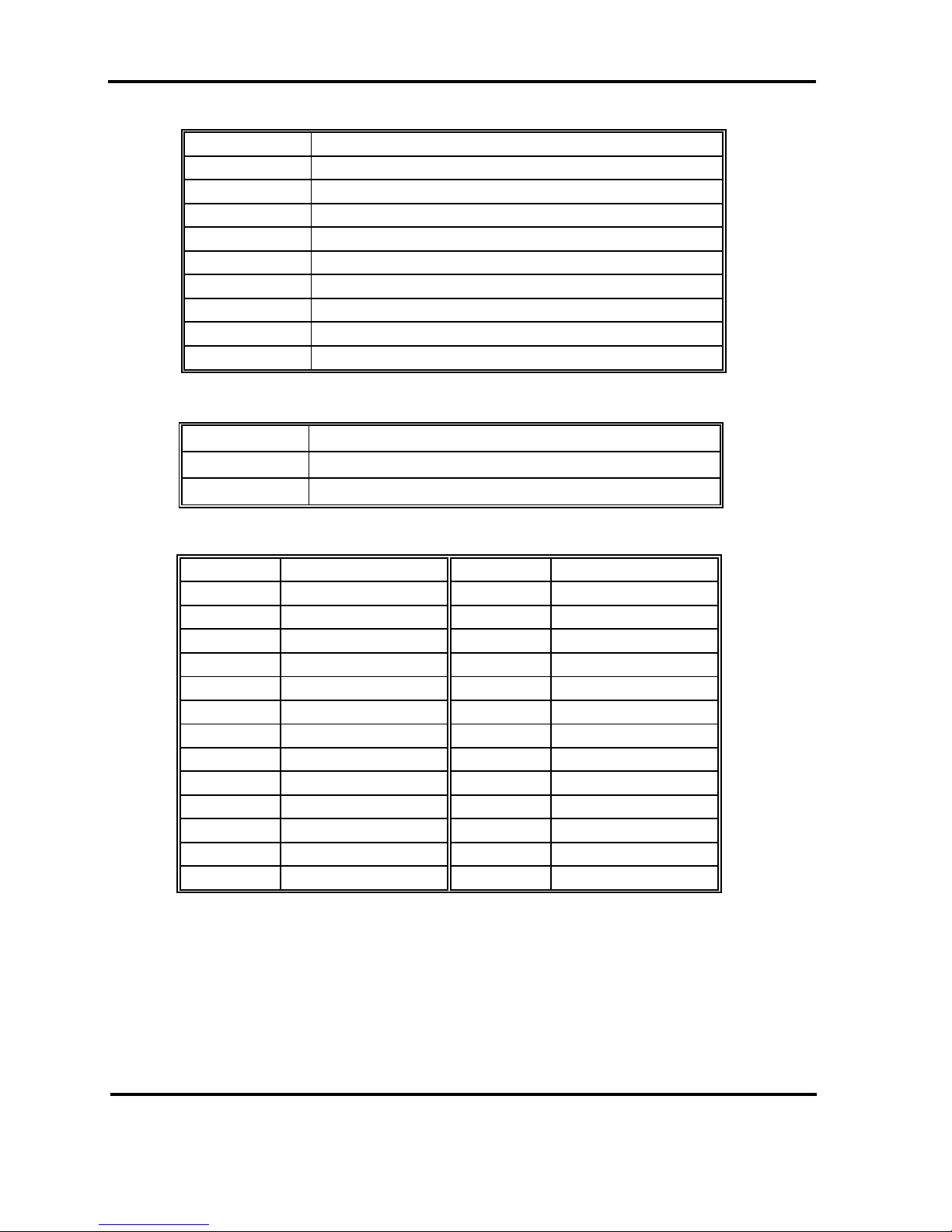
M-System Disk On Chip
S4.1 S4.2 S4.3
Disabled OFF X X
C0000 ON ON ON
C8000 ON ON OFF
D0000 ON OFF ON
*D8000 ON OFF OFF
BIOS Fresh
S4.4
Enabled ON
*Disabled OFF
IRQ12 (Mouse Controller) Release
S4.6
*Enabled ON
Disabled OFF
RTC Clear
S4.5
Enabled ON
*Disabled OFF
COM2 RS232 /RS485/RS422
S7.1 S7.2 S7.3 S7.4 S7.5 S7.6 S7.7 S7.8 S3.1 S3.2 S3.3
*RS232 OFF ON OFF ON OFF ON OFF ON ON OFF OFF
RS485 ON OFF ON OFF ON OFF ON OFF OFF OFF ON
RS422 ON OFF ON OFF ON OFF ON OFF OFF ON OFF
S6.1 S6.2 S6.3 S6.4 S6.5 S6.6 S6.7 S6.8 S3.4 S3.5
*RS232 OFF ON OFF ON OFF ON OFF ON OFF ON
RS485 ON OFF ON OFF ON OFF ON OFF OFF OFF
RS422 ON OFF ON OFF ON OFF ON OFF ON OFF

Peak 632A Us er's Guide
Switches and Connectors
2-3
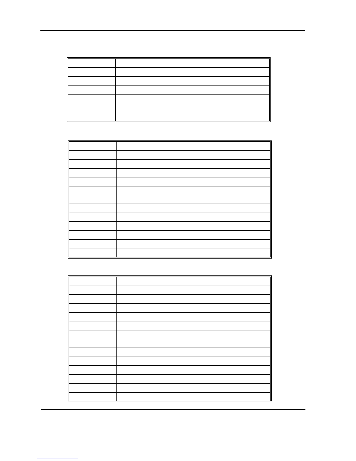
PANEL DIRECTOR
SW2.4 SW2.3 SW2.2 SW2.1
On On On On 1024x768 Dual Scan STN Color Panel
On On On Off 1280x1024 TFT Color Panel
On On Off On 1024x768 Dual Scan STN Color Panel:
On On Off Off 1024x768 Dual Scan STN Color Panel
On Off On On 640x480 Sharp TFT Color Panel
On Off On Off 640x480 18Bit TFT Color Panel
On Off Off On 1024x760 TFT Color Panel
On Off Off Off 800x600 TFT Color Panel
Off On On On 800x600 TFT Color Panel
Off On On Off 800x600 TFT Color Panel
*Off On Off On 800x600 Dual Scan STN Color Panel
Off On Off Off 800x600 Dual Scan STN Color Panel
Off Off On On 1024x768 TFT Color Panel
Off Off On Off 1280x1024 Dual Scan STN Color Panel
Off Off Off ON 1024x600 Dual Scan STN Color Panel
Off Off Off Off 1024x600 TFT Color Panel
PANEL DIRECTOR
SW1.1 SW1.2 SW1.3 SW1.4
*MPCLK From PCLK ON OFF X X
MPCLK From M OFF ON X X
*DE From M X X ON OFF
DE From LP X X OFF ON
FLASH ROM SIZE
S5.1 S5.2
1M ON OFF
*2M OFF ON

Peak 632A Us er's Guide
Switches and Connectors
2-4
2-2 Connectors
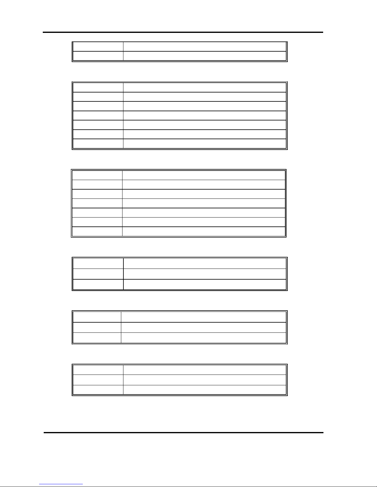
Jumper/Connector define
Connector Function Remark
J1 CPU Fan Header
J2, J3 , J4, J5 DIMM Socket
J7 HDD Connector
J8 Panel Connector
J9 ATX Power Connector
J10 HDD Connector
J11 SCSI Connector
J12 Speaker Connector
J13 FDD Connector
J14 COM2
J15 Reset Connector
J16 Parallel Connector
J17 USB Connector
J18 LAN, RJ45 Connector
J19 CRT Connector
J20 MOUSE Connector
J21 COM1
J22 KB/MS Connector
JP1, JP2, JP3 Temperature Connector
JP5 Panel Voltage Connector
JP6 SMBUS Connector
JP9 ATX Power Button
JP10 NEXCOM ISA Connect or
JP11 IR Connector
JP12 Key Lock
JP13 LAN Link LED
JP14 LAN Speed LED
JP15 LAN Active LED
JP16 HDD LED
JP17 SCSI LED
JP19 Keyboard Connector
JP20 LAN Connector
U21 M-SYSTEM DOC
Peak 632A Us er's Guide
Switches and Connectors
2-5
Pin definitions of connectors
•••• J1: CPU Fan Header Connector
PIN No. Description
1GND
2 +12V
3Sense
• J7 /J10: HDD Connector
PIN No. Description PIN No. Description
1 Reset# 2 Ground
3 Data 7 4 Data 8
5 Data 6 6 Data 9
7 Data 5 8 Data 10
9 Data 4 10 Data 11
11 Data 3 12 Data 12
13 Data 2 14 Data 13
15 Data 1 16 Data 14
17 Data 0 18 Data 15
19 Ground 20 N/C
21 DMA REQ 22 Ground
23 IOW# 24 Ground
25 IOR# 26 Ground
27 IOCHRDY 28 Ground
29 DMA ACK 30 Ground
31 Interrupt 32 NC
33 SA1 34 N/C
35 SA0 36 SA2
37 HDC CS1# 38 HDC CS3#
39 HDD Active# 40 Ground

Peak 632A Us er's Guide
Switches and Connectors
2-6
•••• J8: Flat Panel Connector
PIN No. Description PIN No. Description
1ENABLK 2+12VSAFE
3LP 4DE
5SHFCLK 6FLM
7P0 8VDD
9P2 10P1
11 P4 12 P3
13 P6 14 P5
15 P8 16 P7
17 P10 18 P9
19 P12 20 VDD
21 P14 22 P11
23 GND 24 P13
P16
P15
P18
P17
29 P20 30 ENAVEE
31 P22 32 P19
GND
P21
P24
P23
37 P26 38 P25
39 M/PCLK 40 GND
41 P28 42 P27
43 P30 44 P29
45 P32 46 P31
47 P34 48 P33
49 GND 50 P35
Peak 632A Us er's Guide
Switches and Connectors
2-7
• J9: ATX Power Connect or
PIN No. Description
15VSB
2GND
3Power On
•••• J12: Speaker Connector
PIN No. Description
1 Speaker Signal
2GND
3GND
4+5V
• J13: FDC Connector
PIN No. Description PIN No. Description
1 Ground 2 Density Select
3 Ground 4 N/C
5N/C 6Drate0
7 Ground 8 Index#
9 Ground 10 Motor Enable A#
11 Ground 12 Drive Select B#
13 Ground 14 Drive Select A#
15 Ground 16 Motor Enable B#
17 Ground 18 Direction#
19 Ground 20 Step#
21 Ground 22 Write Data#
23 Ground 24 Write Gate#
25 Ground 26 Track 0#
27 Ground 28 Write Protect#
29 GPI21 30 Read Data#
31 Ground 32 Head Side Select#
33 Ground 34 Disk Change#
Peak 632A Us er's Guide
Switches and Connectors
2-8
• J14/J21: Serial Port Connector (D -Sub 9 -pin)
PIN No. Description
1 Data Carrier Detect (DCD)
2 Receive Data (RXD)
3 Transmit Data (TXD)
4 Data Terminal Ready (DTR)
5 Ground (GND)
6 Data Set Ready (DSR)
7 Request to Send (RTS)
8 Clear to Send (CTS)
9 Ring Indicator (RI)
•••• J15: Reset Connector
PIN No. Description
1 RESET
2GND
• J16: Parallel Port Connector
PIN No. Description PIN No. Description
1 Strobe# 2 Data 0
3 Data 1 4 Data 2
5 Data 3 6 Data 4
7 Data 5 8 Data 6
9 Data 7 10 Acknowledge
11 Bus y 12 Paper Empty
13 Printer Select 14 Auto Form Feed#
15 Error# 16 Initialize
17 Printer Select IN# 18 Ground
19 Ground 20 Ground
21 Ground 22 Ground
23 Ground 24 Ground
25 Ground 26 N/C
Peak 632A Us er's Guide
Switches and Connectors
2-9
• J17: USB Connector
PIN No. Description
1+5V
2USBD03USBDO+
4USBD15USBD1+
6GND
• J18: LAN (RJ45) connector
PIN No. Description
1TD+
2TD3RD+
4TERMPLANE
5TERMPLANE
6RD7 TERMPLANE
8TERMPLANE
9NC
10 NC
11 GND
12 GND
• J19: CRT connector
PIN No. Description
1RED
2 Green
3Blue
4NC
5GND
6GND
7GND
8GND
9+5
10 GND
11 NC
12 Display Data channel data
13 Horizontal Sync
Peak 632A Us er's Guide
Switches and Connectors
2-10
14 Vertical Sync
15 Display Data Channel CLK
• J20: Mouse connecto
r
PIN No. Description
1 Mouse Data
2N/C
3 Ground
4+5V
5 Mouse Clock
6N/C
• J22: Key Board/Mouse Connector
PIN No. Description
1KB/DATA
2 MS/DATA
3GND
45V
5 KB/CLK
6MS/CLK
• JP1/JP2/JP3: Temperature Connector
PIN No. Description
1 Temperature sensor
2GND
• JP5: Panel Voltage
PIN No. Description
1-2 For VDD 5V Panel
2-3 For VDD 3.3V Panel
• JP6: SMBUS Connector
PIN No. Description
SMBCLK
2SMBDATA
Peak 632A Us er's Guide
Switches and Connectors
2-11
• JP9: ATX Power Button
PIN No. Description
+3.3V
2PWRBT#
• JP10: NEXCOM ISA Connector
PIN No. Description PIN No. Description
1 BRSTDRV 2 GND
3VCC 4SD7
5IRQ9 6SD6
7 -12V 8 SD5
9+12V 10SD4
11 GND 12 SD3
13 MEMW# 14 SD2
15 MEMR# 16 SD1
17 IOW# 18 SD0
19 IOR# 20 IOCHRDY
21 REFRESH# 22 BAEN
23 SYSCLK 24 SA9
IRQ7
SA8
IRQ5
SA7
29 IRQ4 30 SA6
31 IRQ3 32 SA5
BALE
SA4
VCC
SA3
37 GND 38 SA2
39 IRQ10 40 SA1
41 IRQ11 42 SA0
43 IRQ12 44 VCC
45 IRQ15 46 MEMR#
47 IRQ14 48 MEMW#
49 MASTER# 50 GND
51 MEMCS16# 52 SA10
53 IOCS16# 54 SA11
55 SBHE# 56 SA12
57 BTC 58 SA13
59 SA15 60 SA14
Peak 632A Us er's Guide
Switches and Connectors
2-12
•••• JP11: IR Connector
PIN No. Description
15V
2 IRRXH
3 IRRX
4GND
5IRTX
• JP12: KEYLOCK Connector
PIN No. Description
1VCC
2N/C
3GND
4KEYLOCK
5GND
• JP13: LAN Link LED
PIN No. Description
1 +3.3V
2LINK#
• JP14: LAN Speed LED
PIN No. Description
1 +3.3V
2 100#
•••• JP15: LAN Active LED
PIN No. Description
1 +3.3V
2ACTIVE#
• JP16: IDE Active LED
PIN No. Description
1+5V
2ACTIVE#
Peak 632A Us er's Guide
Switches and Connectors
2-13
• JP17: SCSI LED
PIN No. Description
1 LED
2+5V
• JP19: Key Board Connector
PIN No. Description
1 Keyboard Clock
2 Keyboard Data
3N/C
4GND
5+5V
• JP20: LAN Connector
PIN No. Description
15V
2 LILED
3RD+
4RD5ACTLED
6TERMPLANE
7N/C
8TERMPLANE
9TD+
6TD-

Peak 632A User's Guide
Capability Expanding 3-
1
Chapter 3
Capability Expanding
This chapter explains how you can expand capability of your CPU board in such
aspects as system memory, cache memory, and CPU.
3-1 System Memory
Your system memory is provided by DIMM's (Dual In-line Memory Modules) on the
CPU board. The CPU board contains four memory banks: Bank 0, 1, 2, 3,
corresponds to connector DIMM1, DIMM2, DIMM3 and DIMM4.
The table below shows possible DIMM configurations for the memory banks.
You can also use the DIMM with parity check. The ECC (Error Checking and
Correction) could be turned on if parity DIMMS are used. The ECC will correct
one bit error and report two bit errors. Please be noted that the PEAK 6320A only
supports the SDRAM.
DIMM 1 DIMM 2 DIMM 3 DIMM 4 Total Memo ry
16M 16M 16M 16M 64MB
32M 32M Empty Empty 64MB
32M 16M 16M Empty 64MB
64M Empty Empty Empty 64MB
32M 32M 32M Empty 96MB
64M 32M Empty Empty 96MB
64M 64M Empty Empty 128MB
32M 32M 32M 32M 128MB
64M 64M 64M Empty 192MB
64M 64M 16M 16M 192MB
64M 64M 64M 64M 256MB
128M Empty Empty Empty 128MB
128M 128M Empty Empty 256MB
128M 128M 128M Empty 384MB
128M 128M 128M 128M 512MB
256M Empty Empty Empty 256MB
256M 256M Empty Empty 512MB
256M 256M 256M Empty 768MB
256M 256M 256M 256M 1GB
Peak 632A User's Guide
Capability Expanding 3-
2
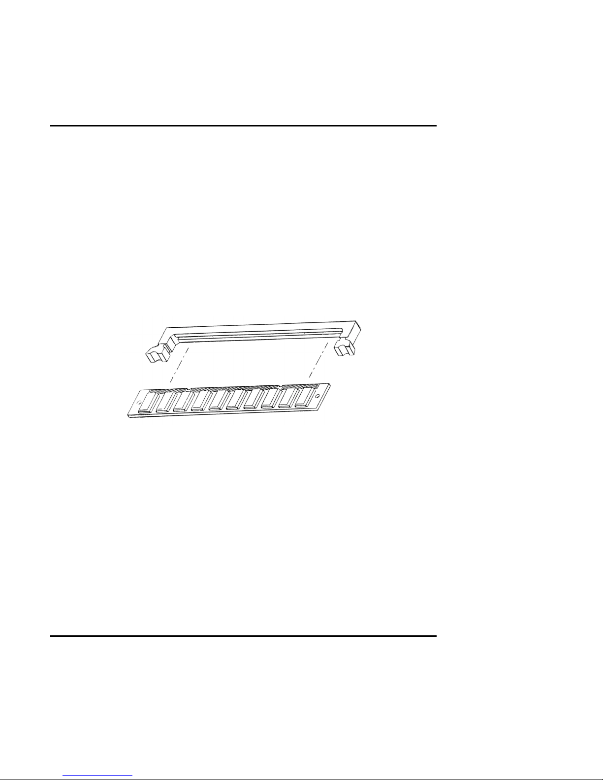
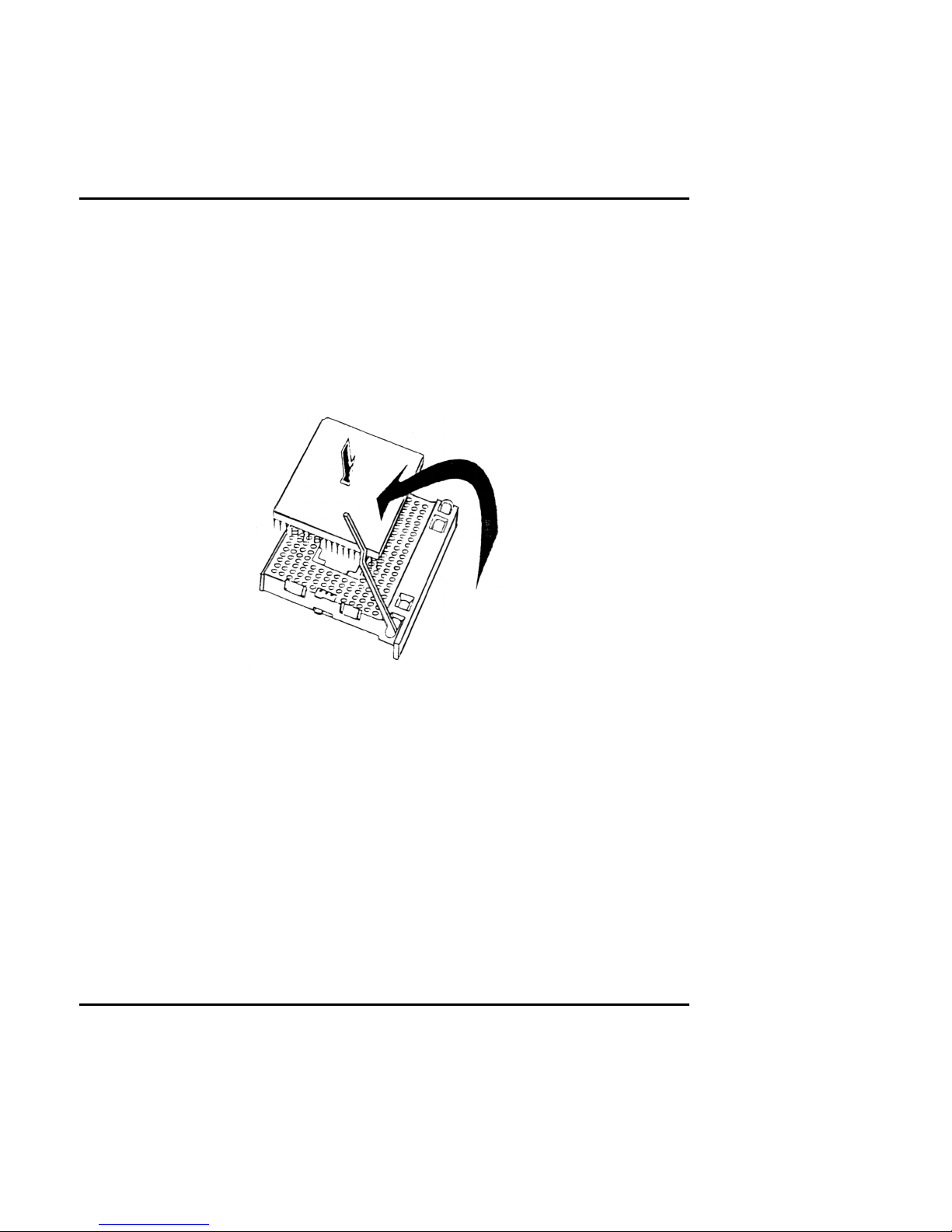
Installing DIMM
To install the DIMM , first make sure the two handles of the DIMM socket are in the
penposition, i.e. the handles stay outward. Slowly slide the DIMM modules
along the plastic guides in the both ends of the socket. Then press the DIMM
module down right into the socket, until a click is heard. That means the two
handles automatically locked the memory modules into the right position of the
DIMM socket as Figure 3-1 shows. To take away the memory module, just push the
both handles outward , the memory module will be ej ected by the mech anism in the
socket.
Figure 3-1 Install DIMM
Peak 632A User's Guide
Capability Expanding 3-
3
3-2 Cache Memory
Since the second level cache has been embedded in to the Pentium II CPU. You do
not have to take care of either SRAM chips or SRAM modu les. The built-in second
level cache in the Pentium II yields much higher performance than the external ones.
The cache size in the Pentium II CPU is either 256KB or 512KB. Normally, for
workstation and server applications, th e 256KB version is good enou gh. However,
if your system is for heavy duty applications, the 512kB version will help a lot.
Specifically for our Pentium II based SBC, the Pentium II has another version
provide much better data security if combined with the DRAM ECC, please check
with your vendor for various Pentium II models.
Figure 3-2 Memory Banks
The level 2 cache of the Peak 6320A is built in the Celeron/Pentium III current
Celerons have 128 KB on die L2 Cache which is very fast because it’s running at the
CPU speed. Future Celerons/Pentium III might be upgr aded to 256 KB L2 Cache.
Peak 632A User's Guide
Capability Expanding 3-
4
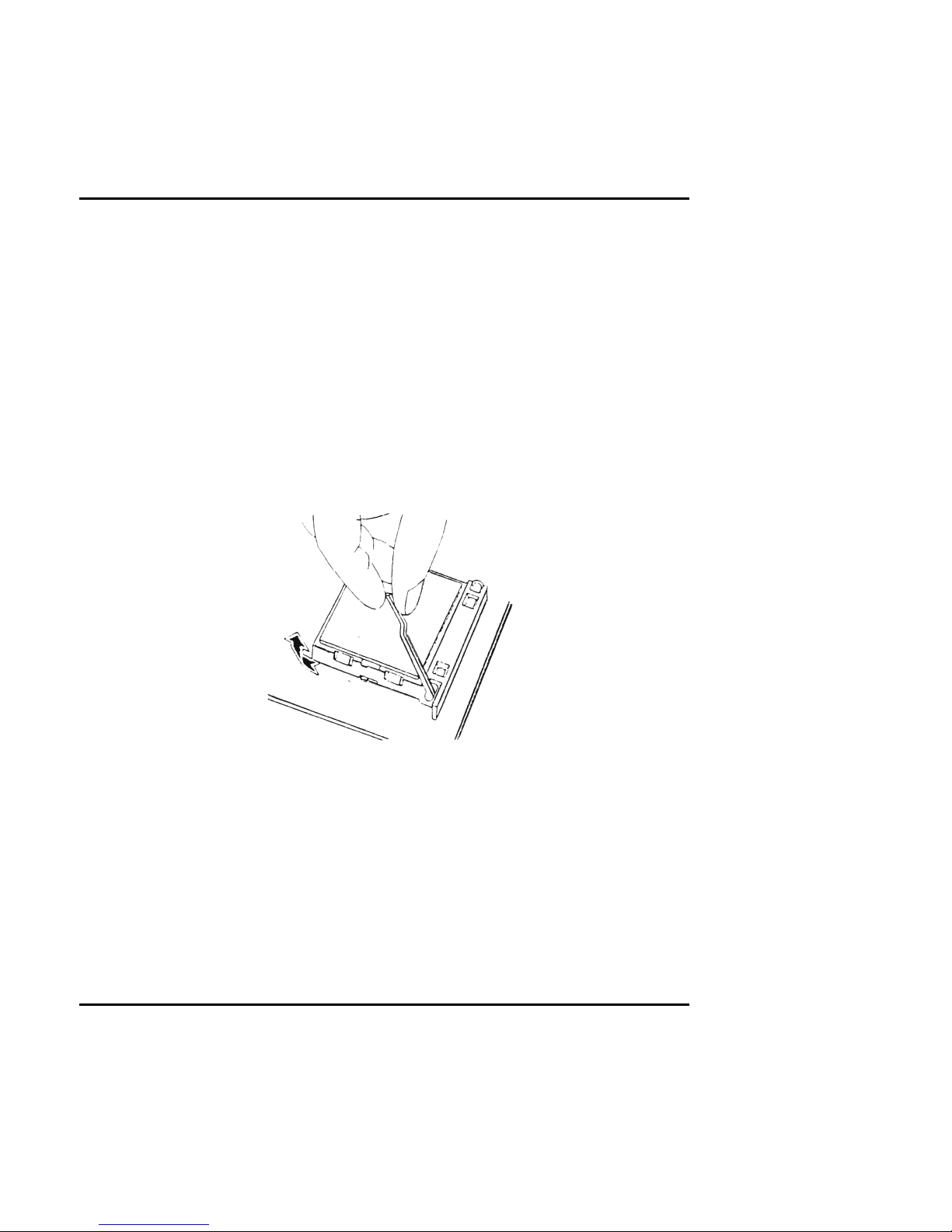
3-3 Change CPU
To change the CPU , pull the handling bar of the socket upward to the other end to
loosen the socket's openings. Carefully lift the existing CPU up to remove it from
the socket.
Figure 3-3 Removing CPU
Peak 632A User's Guide
Capability Expanding 3-
5
Place the new CPU on the middle of the socket, orienting its beveled corner to line up
with the socket's beveled corner. Make sure the pins of the CPU fit even ly to the
socket openings. Replace the handling bar to fasten the CPU to the socket. Be
sure to re-arrange the jumper setting for the correct external clock (66MHz or
100MHz) by (SW1.3) (SW1.4).
Figure 3-4 Installing CPU
 Loading...