PDUKE PFKC05-12D12, PFKC05-12D15, PFKC05-12S05, PFKC05-12S12, PFKC05-12S15 Datasheet
...
x
c
c
A
A
TECHNICAL SPECIFICATION All specifications are typical at nominal input, full load and 25ºC otherwise noted
OUTPUT SPECIFICATIONS
Output power 5 Watts max
Voltage accuracy Full load and nominal Vin ± 2%
Minimum load (Note 1)
Line regulation LL to HL at Full Load
Load regulation
Cross regulation (Dual) Asymmetrical load 25% / 100% FL ± 5%
Ripple and noise 20MHz bandwidth
Temperature coefficient
Transient response recovery time 25% load step change 500uS
Over load protection % of FL at nominal input 180% typ
Short circuit protection Continuous, automatics recovery
INPUT SPECIFICATIONS
Input voltage range
Input filter Pi type
Input surge voltage
100mS max
Input reflected ripple Nominal Vin and full load 150mAp-p
Start up time Nominal Vin and constant resistor load 30mS typ
UL E193009
TUV R50008270
CB JPTUV-003680
CE MARK
25% to 100% FL Single
Dual
3.3V/5V
others
12V nominal input
24V nominal input
48V nominal input
12V input
24V input
48V input
PFKC05-48S05 Derating Curve
10% of FL
1%/p-p of Vout max
I0.02% / ºC, max
9 – 18VDC
18 – 36VDC
36 – 75VDC
100
75
50
Nature convection
25
OUTPUT POWER (%)
0
AMBIENT TEMPERATURE (ºC)
50 60 70 80 90
100 -40 -25 0 -10
• 5 WATTS REGULATED OUTPUT POWER
• 2:1 WIDE INPUT VOLTAGE RANGE
• INTERNATIONAL SAFETY STANDARD APPROVAL
• OVER CURRENT PROTECTION
• HIGH EFFICIE NC Y UP TO 80%
• STANDARD 24 PIN DIP PACKAGE & SMD TYPE PACKAGE
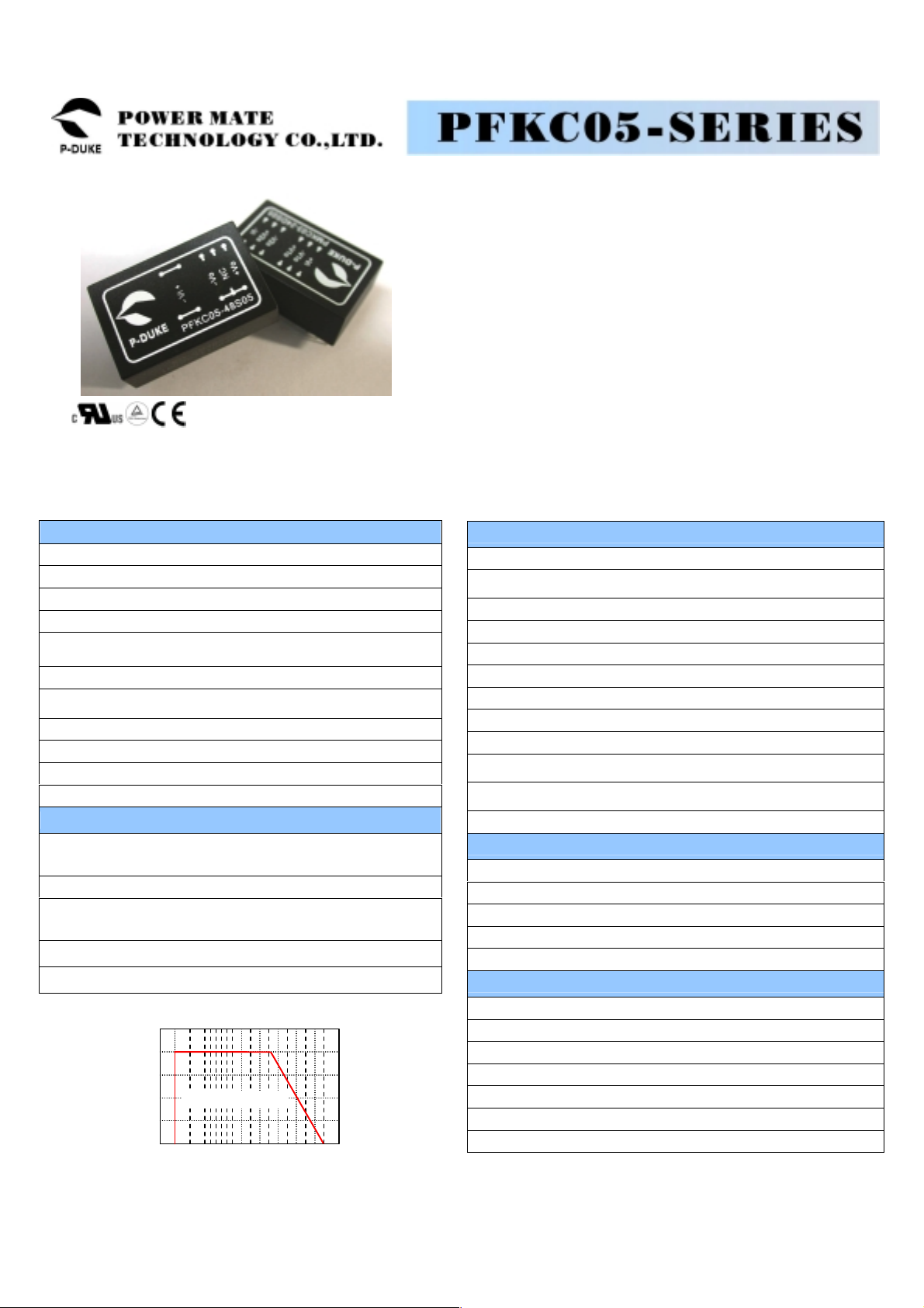
The PFKC05 series offer 5 watts of output power from a package in an IC compatible 24pin
DIP configuration without derating to 71ºC ambient temperature and pin to pin compatible
with PFKC03, FKC03, FKC05 series. PFKC05 series have 2:1 wide input voltage of 9-18,
18-36 and 36-75VDC. The PFKC05 features 1600VDC of isolation and, short-circuit
protection and suffix “ H ” can get 3000VDC isolation. All models are particularly suited to
telecommunications, industrial, mobile telecom and test equipment applications.
GENERAL SPECIFICATIONS
Efficiency See table
± 0.2%
± 0.5%
± 2%
75mVp-p
Isolation voltage Input to Output
Isolation resistance
Isolation capacitance 300pF, ma
Switching frequency 100KHz, min
Approvals and standard IEC60950, UL1950, EN60950
Case material Non-conductive black plasti
Base material Non-conductive black plasti
Potting material Epoxy (UL94-V0)
Dimensions
Weight
MTBF (Note 2) 3.731 x 10⁶hrs
DIP
SMD
Standard
Suffix -H
1.25 X 0.80 X 0.40 Inch
(31.8 X 20.3 X 10.2 mm)
1600VDC, min
3000VDC, min
109ohms, min
14g (0.48oz)
15g (0.52oz)
ENVIRONMENTAL SPECIFICATIONS
Operating temperature range -25ºC ~ +71ºC
36VDC
50VDC
100VDC
Storage temperature range -55ºC ~ +105ºC
Thermal shock MIL-STD-810D
Vibration 10~55Hz, 2G, 30minutes along X,Y and Z
Relative humidity 5% to 95% RH
EMC CHARACTERISTICS
Conducted emissions EN55022 Level
Radiated emissions EN55022 Level
ESD EN61000-4-2 Perf. Criteria2
Radiated immunity EN61000-4-3 Perf. Criteria2
Fast transient EN61000-4-4 Perf. Criteria2
Surge EN61000-4-5 Perf. Criteria2
Conducted immunity EN61000-4-6 Perf. Criteria2

(4)
(5)
Model
Number
PFKC05-12S33 9 – 18 VDC 3.3 VDC 1000mA
PFKC05-12S05 9 – 18 VDC 5 VDC 1000mA
PFKC05-12S12 9 – 18 VDC 12 VDC 470mA 618mA 80 220uF
PFKC05-12S15 9 – 18 VDC 15 VDC 400mA 658mA 80 150uF
PFKC05-12D05 9 – 18 VDC ± 5 VDC ± 500mA 571mA 77 ± 680uF
PFKC05-12D12 9 – 18 VDC ± 12 VDC ± 230mA 605mA 80 ± 100uF
PFKC05-12D15 9 – 18 VDC ± 15 VDC ± 190mA 625mA 80 ± 68uF
PFKC05-24S33 18 – 36 VDC 3.3 VDC 1000mA 202mA 72 2200uF
PFKC05-24S05 18 – 36 VDC 5 VDC 1000mA 278mA 79 1000uF
PFKC05-24S12 18 – 36 VDC 12 VDC 470mA 306mA 81 220uF
PFKC05-24S15 18 – 36 VDC 15 VDC 400mA 325mA 81 150uF
PFKC05-24D05 18 – 36 VDC ± 5 VDC ± 500mA 282mA 78 ± 680uF
PFKC05-24D12 18 – 36 VDC ± 12 VDC ± 230mA 299mA 81 ± 100uF
PFKC05-24D15 18 – 36 VDC ± 15 VDC ± 190mA 309mA 81 ± 68uF
PFKC05-48S33 36 – 75 VDC 3.3 VDC 1000mA 100mA 73 2200uF
PFKC05-48S05 36 – 75 VDC 5 VDC 1000mA 141mA 78 1000uF
PFKC05-48S12 36 – 75 VDC 12 VDC 470mA 153mA 81 220uF
PFKC05-48S15 36 – 75 VDC 15 VDC 400mA 162mA 81 150uF
PFKC05-48D05 36 – 75 VDC ± 5 VDC ± 500mA 143mA 77 ± 680uF
PFKC05-48D12 36 – 75 VDC ± 12 VDC ± 230mA 149mA 81 ± 100uF
PFKC05-48D15 36 – 75 VDC ± 15 VDC ± 190mA 154mA 81 ± 68uF
Note
1. The PFKC05 series required a minimum 10% loading on the output to maintain specified regulation. Operation under no-load condition will not damage
these devices, however they may not meet all listed specification
2. BELLCORE TR-NWT-000332. Case I: 50% Stress, Temperature at 40ºC. (Ground fixed and controlled environment)
3. Maximum value at nominal input voltage and full load of standard type.
4. T y pical value at nominal input voltage and full load.
5. Test by minimum Vin and constant resistor load.
Input
Range
Output
Voltage
Output
Current
Input
Current
404mA
579mA
Eff
(3)
(%)
72 2200uF
76 1000uF
Capacitor
Load max
Pin size is 0. 02(0.5) Dia or
0.01 x 0.02 (0.25 x 0.50)
Rectangular Pin
0.18(4.6)
23
2
3
22
BOTTOM
VIEW
16
9
10
15
14
11
0.60(15.2)
0.80(20.3)
0.90 (22.9)
0.15
(3.8)
1.00(25.4)
0.92(23.4)
24
0.02(0.5)
20
BOTTOM
0.20 (5.1)
1.25 (31.8)
Pin Area
0.40
(10.2)
1. All dimensions in Inches (mm)
2. Pin pitch tolerance I0.014(0.35)
0.04 x 0.02
(1.0 x 0.5)
VIEW
16
13
0.80(20.3)
Suffix-SMD
1
5
9
12
0.44(11.2)
0.43(10.9)
0.10 (2.54)
0.15 (3.81) 0.25 (6.35)
1.26 (32.0)
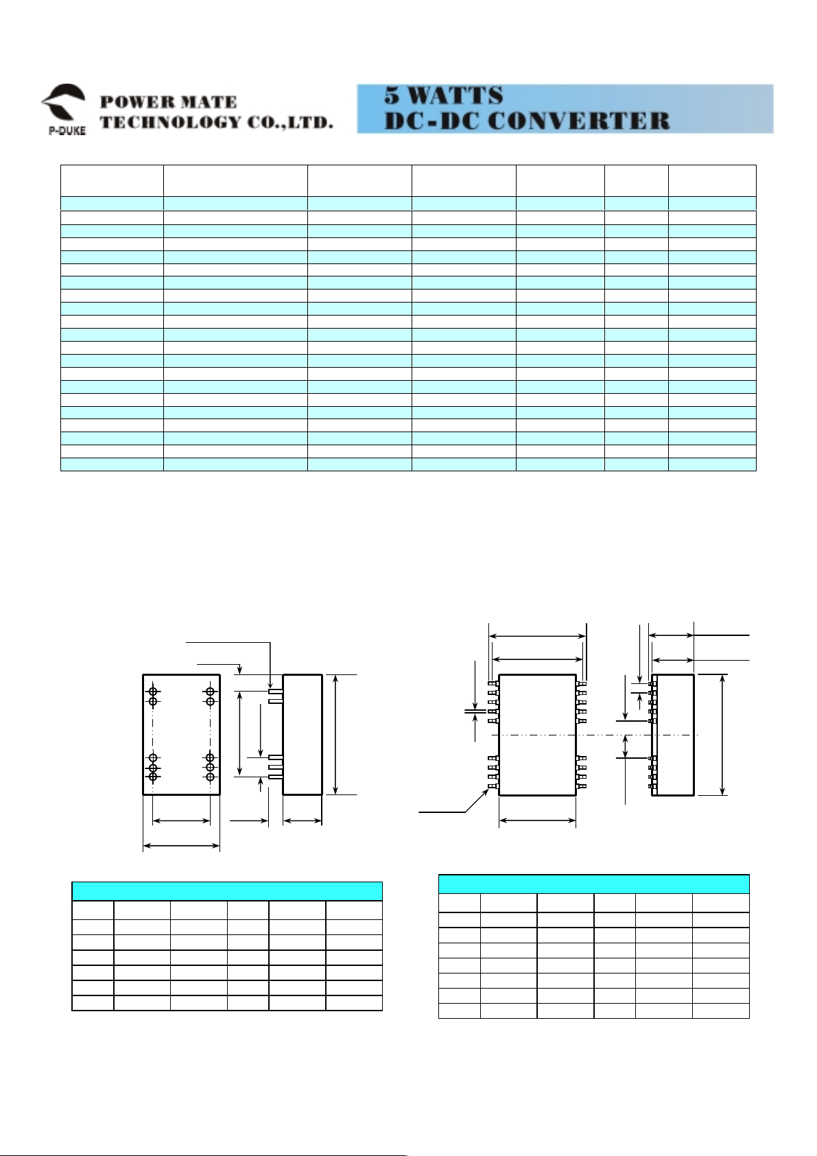
DIP PIN CONNECTI ON
PIN SINGLE DUAL
2 - INPUT - INP U T
3 - INPUT - INP U T
9 NC
10 NC NC 15 NC NC
11 NC - OUTPUT 14 + OUTPUT + OUTPUT
COMMON
PIN SINGLE DUAL
23 + INPUT + INPUT
22 + INPUT + INPUT
16 - OUTPUT COMMON
PIN SINGLE DUAL
2 - INPUT - INP U T
3 - INPUT - INP U T
9 NC
10 NC NC 15 NC NC
11 NC - OUTPUT 14 + OUTPUT + OUTPUT
Others NC NC Others NC NC
SMD PIN CONNECTI ON
PIN SINGLE DUAL
23 + INPUT + INPUT
22 + INPUT + INPUT
COMMON
16 - OUTPUT COMMON
 Loading...