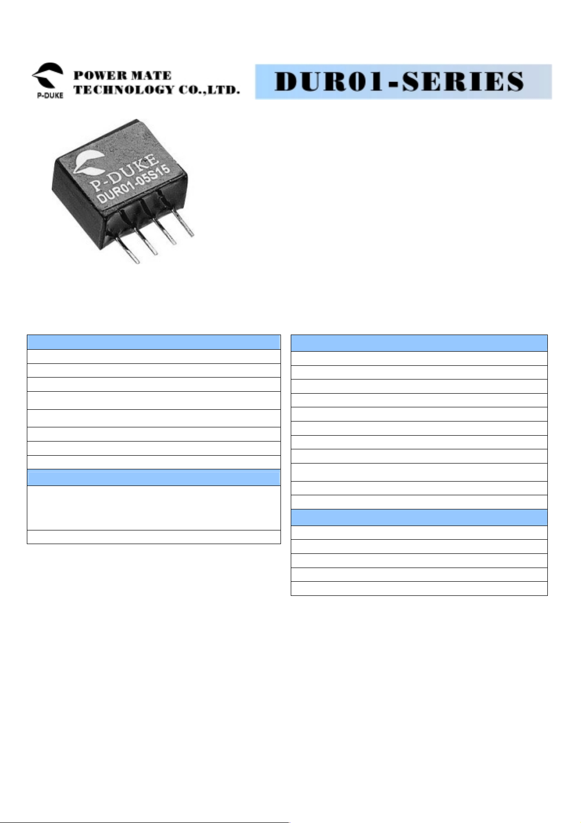
P-DUKE DUR01-15S33, DUR01-15S15, DUR01-15S12, DUR01-15S05, DUR01-12S33 Datasheet
...
• 1 WATT UNREGULATED OUTPUT POWER
• 4 PIN SINGLE-IN-LINE PACKAGE (SIP)
• HIGH EFFICIENCY FOR LOW POWER APPLICATION
• UL 94-V0 NON-CONDUCTED C ASE
• INTERNAL INPUT & O UTP U T FILTER
• INPUT / OUTPUT ISOLATION UP TO 1KVDC
The DUR01 series are the standard building blocks for on-board distributed power
systems. They are ideally suited to providing single and dual supplies on primarily
digital boards with added benefit of galvanic isolation to reduce switching noise. All
of the rated power may be drawn from a single pin provided the total load does not
exceed 1 watt.
TECHNICAL SPECIFICATION All specifications are typical at nominal input, full load and 25ºC otherwise noted
OUTPUT SPECIFICATIONS
Output power
Voltage accuracy Full load and nominal Vin ± 5%
Minimum load (Note 1) 10% of FL
Line regulation LL to HL at Full Load
Load regulation 10% to 100% FL
Ripple and noise 20MHz bandwidth 100mVp-p
T e mperature coefficient
Short circuit protection Short term
3.3V & 5V output
others
3.3V & 5V output
others
1 Watt max
1.3%/1% of Vin
1.2%/1% of Vin
± 15%
± 10%
I0.1% / ºC, max
INPUT SPECIFICATIONS
Input voltage range
Input filter Capacitor
3.3V nominal input
5V nominal input
12V nominal input
15V nominal input
24V nominal input
3.0 – 3.6VDC
4.5 – 5.5VDC
10.8 – 13.2VDC
13.5 – 16.5VDC
21.6 – 26.4VDC
GENERAL SPECIFICATIONS
Efficiency See table
Isolation voltage 1000VDC, min
Isolation resistance
Isolation capacitance 80pF, typ.
Switching frequency 90KHz, typ
Design meet safety standard UL1950, EN60950
Case material Non-conducted black plastic
Potting material Epoxy (UL94-V0)
Dimensions
Weight 1.5g (0.053oz)
MTBF (Note 2) 1.137 x 10⁹ hrs
0.45 X 0.24 X 0.40 Inch
(11.5 X 6.0 X 10.2 mm)
9
10
ohms, min
ENVIRONMENTAL SPECIFICATIONS
Operating temperature range -40ºC ~ +85ºC (with derating)
Storage temperature range -55ºC ~ +105ºC
Thermal shock MIL-STD-810D
Vibration 10~55Hz, 2G, 30minutes along X,Y and Z
Relative humidity 5% to 95% RH

(4)
Model
Number
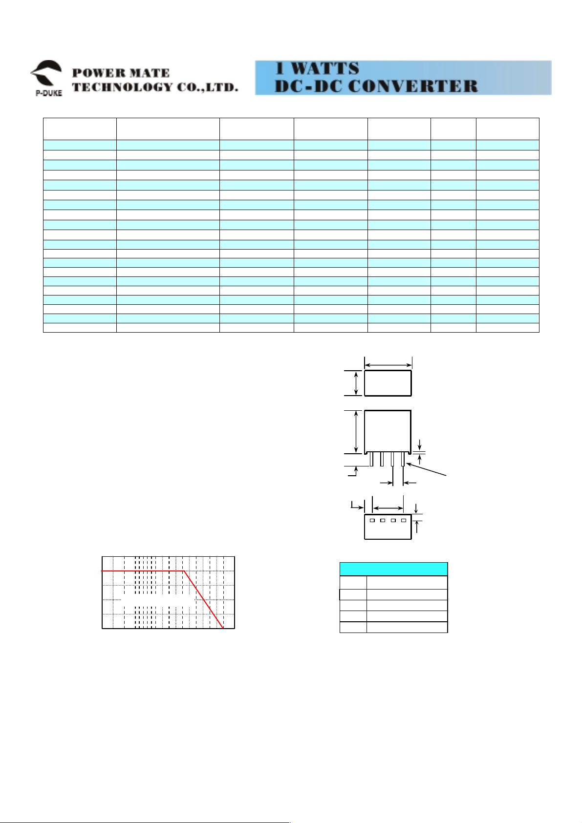
DUR01-33S33 3.0 – 3.6 VDC 3.3 VDC 303mA
DUR01-33S05 3.0 – 3.6 VDC 5 VDC 200mA
DUR01-33S12 3.0 – 3.6 VDC 12 VDC 84mA
DUR01-33S15 3.0 – 3.6 VDC 15 VDC 66mA
DUR01-05S33 4.5 – 5.5 VDC 3.3 VDC 303mA
DUR01-05S05 4.5 – 5.5 VDC 5 VDC 200mA
DUR01-05S12 4.5 – 5.5 VDC 12 VDC 84mA
DUR01-05S15 4.5 – 5.5 VDC 15 VDC 66mA
DUR01-12S33 10.8 – 13.2 VDC 3.3 VDC 303mA
DUR01-12S05 10.8 – 13.2 VDC 5 VDC 200mA
DUR01-12S12 10.8 – 13.2 VDC 12 VDC 84mA 113mA 78 6.2uF
DUR01-12S15 10.8 – 13.2 VDC 15 VDC 66mA 109mA 80 6.2uF
DUR01-15S33 13.5 – 16.5 VDC 3.3 VDC 303mA 105mA 68 6.2uF
DUR01-15S05 13.5 – 16.5 VDC 5 VDC 200mA 101mA 70 6.2uF
DUR01-15S12 13.5 – 16.5 VDC 12 VDC 84mA 91mA 78 6.2uF
DUR01-15S15 13.5 – 16.5 VDC 15 VDC 66mA 87mA 80 6.2uF
DUR01-24S33 21.6 – 26.4 VDC 3.3 VDC 303mA 64mA 70 6.2uF
DUR01-24S05 21.6 – 26.4 VDC 5 VDC 200mA 63mA 70 6.2uF
DUR01-24S12 21.6 – 26.4 VDC 12 VDC 84mA 57mA 78 6.2uF
DUR01-24S15 21.6 – 26.4 VDC 15 VDC 66mA 54mA 80 6.2uF
Note
1. The DUR01 series required a minimum 10% loading on the output to
maintain specified regulation. Operation under no-load condition will not
damage these devices, however they may not meet all listed
specification
2. BELLCORE TR-NWT-000332. Case I: 50% Stress, Temperature at 40ºC.
(Ground fixed and controlled environment)
3. Maximum value at nominal input voltage and full load of standard type.
4. Typical value at nominal input voltage and full load.
5. Test by minimum Vin and constant resistor load.
Input
Range
Output
Voltage
DUR01-24S05 Derating Curve
Output
Current
0.24(6.0)
0.40(10.2)
0.16(4.1)
0.08(2.03)
Input
Current
473mA
451mA
449mA
423mA
312mA
303mA
272mA
262mA
131mA
126mA
0.45(11.5)
FRONT VIEW
0.30(7.6)
12 43
BOTTOM VIEW
Eff
(3)
0.05(1.2)
(%)
68 6.2uF
70 6.2uF
72 6.2uF
75 6.2uF
68 6.2uF
70 6.2uF
78 6.2uF
80 6.2uF
68 6.2uF
70 6.2uF
0.02(0.5)
0.01x 0.02 ( 0.25 x 0.5)
0.10(2.5)
Rectangular Pin
All dimensions in Inches (mm)
Pin pitch tolerance I0.014(0.35)
Capacitor
Load max
(5)
100
75
50
25
OUTPUT POWER (%)
0
Nature convection
50 60 70 80 90
AMBIENT TE M P E RATURE (ºC)
100 -40 -25 0 -10
STANDARD
PIN SINGLE
1 - INPU T
2 + INPUT
3 - OUTPU T
4 + OUTPUT
 Loading...