

Page 1

Electronic Emission Notices
Federal Communications Commission (FCC) Statement
This equipment has been tested and found to comply with the limits for a
Class B digital device, pursuant to Part 15 of FCC Rules. These limits are
designed to provide reasonable protection against harmful interference in a
residential installation. This equipment generates, uses and can radiate radio
frequency energy and, if not installed and used in accordance with instructions
contained in this manual, may cause harmful interference to radio and
television communications. However, there is no guarantee that interference
will not occur in a particular installation.
If this equipment does cause harmful interference to radio or television
reception, which can be determined by turning the equipment off and on, the
user is encouraged to try to correct the interference by one or more of the
following measures:
- REORIENT OR RELOCATE THE RECEIVING ANTENNA
- INCREASE THE SEPARA TION BETWEEN THE EQUIPMENT AND THE RECEIVER
- CONNECT THE EQUIPMENT INTO AN OUTLET ON A CIRCUIT DIFFERENT FROM
THAT OF THE RECEIVER
- CONSULT THE DEALER OR AN EXPERIENCED AUDIO/TELEVISION TECHNICIAN
NOTE: Connecting this device to peripheral devices that do not comply with
Class B requirements, or using an unshielded peripheral data cable,
could also result in harmful interference to radio or television reception.
The user is cautioned that any changes or modifications not expressly
approved by the party responsible for compliance could void the user’s
authority to operate this equipment.
T o ensure that the use of this product does not contribute to interference,
it is necessary to use shielded I/O cables.
Copyright
This manual is copyrighted with all rights reserved. No portion of this manual may be
copied or reproduced by any means.
While every precaution has been taken in the preparation of this manual, no responsibility
for errors or omissions is assumed. Neither is any liability assumed for damages resulting
from the use of the information contained herein.
1
Trademarks
All brand names, logos and registered trademarks mentioned are property of their
respective owners.
Page 2

2
Table of Contents
HARDWARE CONFIGURATION ............................................................................. 3
Key Features ............................................................................................... 3
Motherboard Layout (Model Code No. - 35889700XX) ............................... 5
Jumper Settings .......................................................................................... 6
CPU Type Selection - JP1, JP2, JP3, JP4, JP5, JP6, JP8,
JP11, JP39, JP40................................................................................... 6
Intel® MMX CPU.................................................................................... 6
Intel® CPU ............................................................................................. 6
IDT® WinChip C6 CPU.......................................................................... 7
AMD® CPU............................................................................................. 7
Cyrix®/IBM® CPU................................................................................... 8
JP10 - System Memory Tuning Jumper ................................................ 9
JP31 - CMOS Clear................................................................................ 9
JP36 - BIOS Program Voltage / BIOS Select ......................................... 9
JP41 - Selection for on Board AC97 or AMR AC97 Sound.................... 9
Pin List of Special Connectors .............................................................. 1 0
Memory Configuration ................................................................................. 11
Installation ................................................................................................... 11
Installing a DRAM Module ..................................................................... 11
Installing the Processor ........................................................................ 1 2
BIOS SETUP ............................................................................................... 1 3
Starting Setup .............................................................................................. 13
Main Menu ................................................................................................... 13
Standard CMOS Setup ................................................................................ 15
BIOS Features Setup................................................................................... 16
Chipset Features Setup .............................................................................. 17
Power Management Setup .......................................................................... 17
PNP/PCI Configuration Setup ..................................................................... 17
Integrated Peripherals ................................................................................ 17
Supervisor/User Password Setting ............................................................ 1 7
Flash Update Procedure ............................................................................. 1 8
APPENDIX - Technical Reference .......................................................... 1 9
CPU to Bus Frequency Ratio (JP1, JP2, JP6) ............................................ 19
CPU External Clock (BUS) Frequency (JP3, JP4, JP5, JP8) ...................... 19
CPU Core Voltage (JP11) .......................................................................... 20
JP39, JP40 - CPU Power Supply ............................................................. 2 0
Technical Reference Booklet
Page 3

HARDWARE CONFIGURATION
This motherboard is based on the VIA® Apollo MVP4 Chipset. The chipset is a
highly integrated solution for a cost-effective and compact motherboard.
Features include internal AGP Version 2.0 compliant, PCI bus master IDE, PCI
Ver 2.2 compliance, AC 97 Codec Sound. DIMM sockets are provided on board,
allowing flexible installation of main memory. The on board pipelined burst
cache further boosts the system performance.
Key Features
Processor
• ZIP socket 7
• Fully support Intel® Pentium® processors with MMX technology using
socket 7.
• Support Pentium® processors operating from 100MHz to 233MHz.
• Support Cyrix®/IBM® 6x86/6x86L/6x86MX/M-II processors.
• Support AMD® K5/K6/K6-2/K6-III processors.
• Support IDT® WinChip C6 processors.
Cache
• Direct-mapped L2 write-back cache.
• Supports 512KB on board synchronous pipelined burst SRAM.
Memory Organiztion
• Supports 3.3V Extended Data Output(EDO) DRAM at 50 and 60ns speeds.
• Memory size up to 256MB.
• Supports single-density DIMMs of 1MB, 2MB, 4MB, 8MB and 16MB depth
(x64 or 72).
• Supports double-density DIMMs of 2MB, 4MB, 8MB, 16MB and 32MB
depth (x64 or 72).
On-Chip I/O
• Two PCI fast IDE ports supporting up to four ATA Device(Including IDE
HDDs, CD-ROMs, ZIP and LS-120 drives).
• Supports bus master IDE, PIO mode 4(up to 16MB/sec), Ultra DMA33
(up to 33MB/sec) and Ultra DMA66(up to 66MB/sec) transfer.
• One ECP/EPP parallel port.
• Two 16550-compatible UART serial ports.
• One floppy port supporting two FDDs of 360KB, 720KB, 1.2M, 1.44M or
2.88M formatted capacity.
• Four USB ports.
• One PS/2 type keyboard port.
• PS/2 mouse port.
• Infrared (IrDA) support (via a header).
• VGA port.
3
Hardware Setup
Page 4

4
AC97 Digital Audio Controller
• Dual full-duplex Direct Sound Channels between system memory and
AC97 Link.
• Standard AC97 Codec interface for multimedia systems.
• Complete software driver support for Windows® 95/98.
• Direct game port and one MIDI port interface.
System BIOS
• 2MB flash BIOS supporting PnP, APM, ACPI and windows® 9X.
• Auto detects and supports LBA hard disks with formatted capacities
over 8.4GB.
• Easily upgradable by end-user.
Plug-and-Play
• Supports plug-and-play specification 1.0a.
• Plug-and-play for Windows® 9X.
• Fully steerable PCI interrupts.
Power Management
• Supports SMM, APM and ACPI.
• Break switch for instant suspend/resume on system operation.
• Energy star “Green PC” compliant.
• Support Wake on Lan.
Expansion Slots
• 3 PCI bus master slots (rev. 2.2 compliant).
• 1 ISA slot.
• 1 AMR slot.
PC97/PC98
• PC97/PC98 ready.
Technical Reference Booklet
Page 5
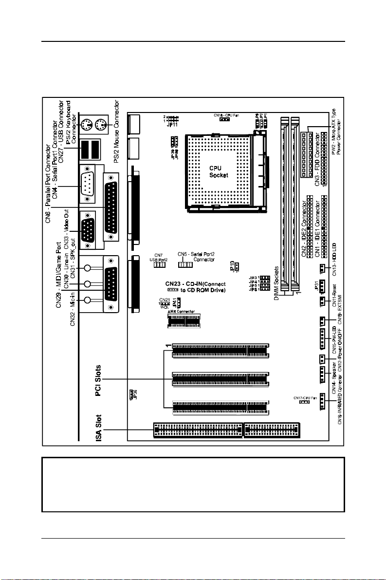
Motherboard Layout (Model Code No. - 35889700XX)
The following diagram shows the relative positions of the jumpers, connectors,
major components and memory banks on the motherboard.
1
1
1
1
1
5
Warning:
All connectors on board are labeled Pin “1” at one conner. Ribbon
cables should always be connected with the red stripe on the Pin
“1” side of the connector.
Hardware Setup
Page 6
6
Jumper Settings
This section explains how to configure the motherboard’s hardware. Before
using your computer, make sure all jumpers and DRAM modules are set
correctly. Refer to this chapter whenever in doubt.
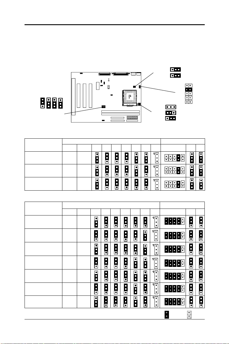
CPU Type and Voltage Selection Jumper - JP1, JP2, JP3, JP4, JP5, JP6,
JP8, JP11, JP39, JP40
JP39
JP40
1
1
2
1
JP11
1
1
1
1
1
JP8
JP5
JP4
JP3
JP6
JP2
JP1
1
1
Intel® MMX CPU
CPU Type & Speed CPU, PCI Bus Clock & CPU Type CPU Voltage
CPU MHz PCI MHz JP3 JP4 JP5 JP8 JP1 JP2 JP6 JP11 JP39 JP40
Intel Pentium-166MMX 66MHz 33MHz
Intel Pentium-200MMX 66MHz 33MHz
Intel Pentium-233MMX 66MHz 33MHz
1
1
1
1
1
1 1
1
11 1
1
1
11 1
1
1
2
1
2
1
2
1
1 1
1
1 1
1
Intel® CPU (Intel® Pentium® CPU without MMX Technology)
CPU Type & Speed CPU, PCI Bus Clock & CPU Type CPU Voltage
CPU MHz PCI MHz JP3 JP4 JP5 JP8 JP1 JP2 JP6 JP11 JP39 JP40
Intel Pentium-100 66MHz 33MHz
Intel Pentium-120 60MHz 30MHz
Intel Pentium-133 66MHz 33MHz
Intel Pentium-150 60MHz 30MHz
Intel Pentium-166 66MHz 33MHz
Intel Pentium-180 60MHz 30MHz
Intel Pentium-200 66MHz 33MHz
Technical Reference Booklet
1
111
111
111
1
1
1
1
1
1
11
1
1
11
1
1
11
1
1
1
1
1
1
1
1
1
1
1
1
1
1
1
1
2
1
2
1
2
1
2
1
2
1
2
1
2
1
Close Open
1 1
1 1
1 1
1 1
1
1 1
1 1
1
Page 7
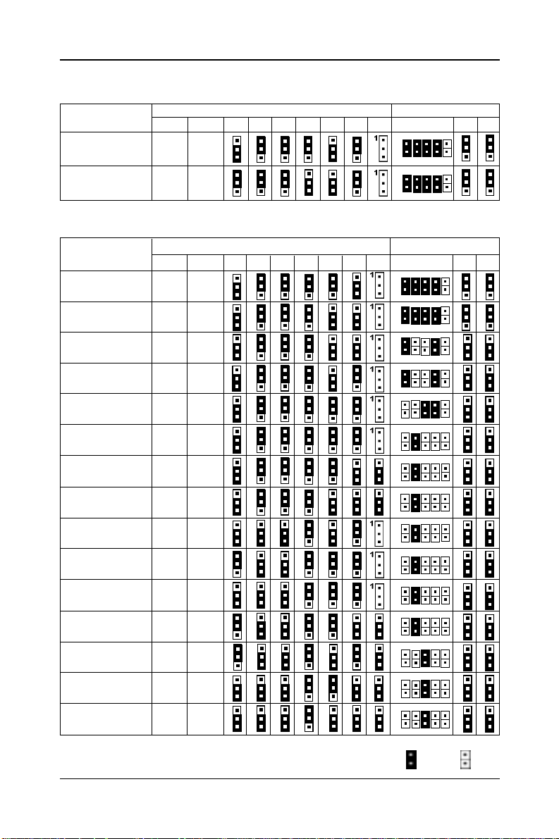
IDT® WinChip C6 CPU
CPU Type & Speed CPU, PCI Bus Clock & CPU Type CPU Voltage
CPU MHz PCI MHz JP3 JP4 JP5 JP8 JP1 JP2 JP6 JP11 JP39 JP40
IDT WinChip C6-200 66MHz 33MHz
IDT WinChip C6-225 75MHz 37.5MHz
1
1
1
1
1
AMD® CPU
CPU Type & Speed CPU, PCI Bus Clock & CPU Type CPU Voltage
CPU MHz AGP MHz JP3 JP4 JP5 JP8 JP1 JP2 JP6 JP11 JP39 JP40
AMD-K5-PR133 66MHz 33MHz
AMD-K5-PR166 66MHz 33MHz
AMD-K6-166 66MHz 33MHz
AMD-K6-200 66MHz 33MHz
AMD-K6-233(3.2V) 66MHz 33MHz
AMD-K6-233(2.2V) 66MHz 33MHz
AMD-K6-266 66MHz 33MHz
AMD-K6-300 66MHz 33MHz
AMD-K6-2/300* 100MHz* 33MHz*
AMD-K6-2/333 95MHz 31.75MHz
AMD-K6-2/350 100MHz 33MHz
AMD-K6-2/380 95MHz 31.75MHz
AMD-K6-2/475 95MHz 31.75MHz
AMD-K6-III/400 100MHz 33MHz
AMD-K6-III/450 100MHz 33MHz
111
111
111
1 1
1
111
111
111
1
1
1
1
1
1
1
1
1
1
1
1
1
11
1
11
1
1
11
11
1
1
1
1
1
1
1
1
1
1
1
1
1
1
1
1
11
11
1
1
1
1
1
1
1
1
1
1
1
1
1
1
1
1
1
1
1
1
1
1
1 1
11
1
1
1
1 1
1
1
2
1
2
1
2
1
2
1
2
1
2
1
2
1
2
1
1
2
1
1
2
1
2
1
2
1
2
1
2
1
1
2
1
2
1
11
2
1
1 1
1
1
1
1 1
1
1
1
1
1 1
1
1
1 1
1 1
1 1
1 1
1
7
1
1
1
1
1
1
1
1
1
1
* = Default setting (AMD-K6-2/300 CPU)
Close Open
Hardware Setup
Page 8
8
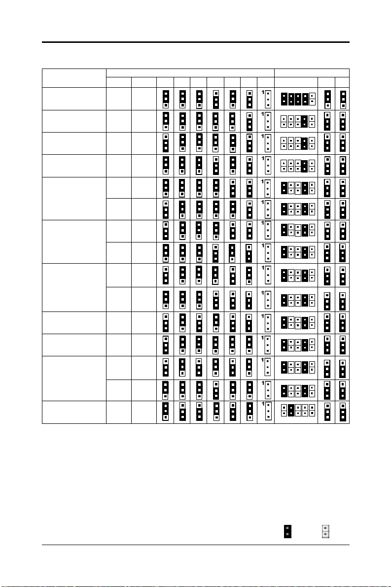
Cyrix®/IBM® CPU
CPU Type & Speed CPU, PCI Bus Clock & CPU Type CPU Voltage
Cyrix/IBM 6x86-PR200+ 75MHz 37.5MHz
Cyrix/IBM 6x86L-PR150+ 60MHz 30MHz
Cyrix/IBM 6x86L-PR166+ 66MHz 33MHz
Cyrix/IBM 6x86L-PR200+ 75MHz 37.5MHz
Cyrix/IBM 6x86MX-PR166
Cyrix/IBM 6x86MX-PR200
Cyrix/IBM 6x86MX-PR233
Cyrix MII 6x86MX-PR266 83MHz 27.77MHz
Cyrix MII 6x86MX-PR300 66MHz 33MHz
Cyrix MII 6x86MX-PR333
Cyrix MII 6x86MX-PR400 95MHz 31.75MHz
CPU MHz PCI MHz JP3 JP4 JP5 JP8 JP1 JP2 JP6 JP11 JP39 JP40
111
1 11
60MHz 30MHz
66MHz 33MHz
66MHz 33MHz
75MHz 37.5MHz
66MHz 33MHz
75MHz 37.5MHz
83MHz 27.77MHz
75MHz 37.5MHz
1
111
111 1
1
1 11
1
111
1
111 1
1 1
1
1
1
1
1
11
1
1
1
111 1
1
11
1
1
1
1
1
1
1
1
1
1 1
1 1
1
1
1
1
1
1
1
1
1
1
1
1
1111
11 11
1
1
1
1
1
1
1
1
1
1
1
2
1
2
1
2
1
2
1
2
1
2
1
2
1
2
1
2
1
2
1
2
1
2
1
2
1
2
1
2
1
1
111
1 1
1
1 1
1 1
1
1 1
1 1
1
1
1
1
1
1
1
1
1
1
1
1
1
1
Technical Reference Booklet
Close Open
Page 9
1
JP39
JP40
JP6
JP2
JP1
JP10
1
2
1
JP1 1
1
1
1
1
JP8
JP36
1
JP41
1
1
JP5
JP31
1
1
JP4
1
JP3
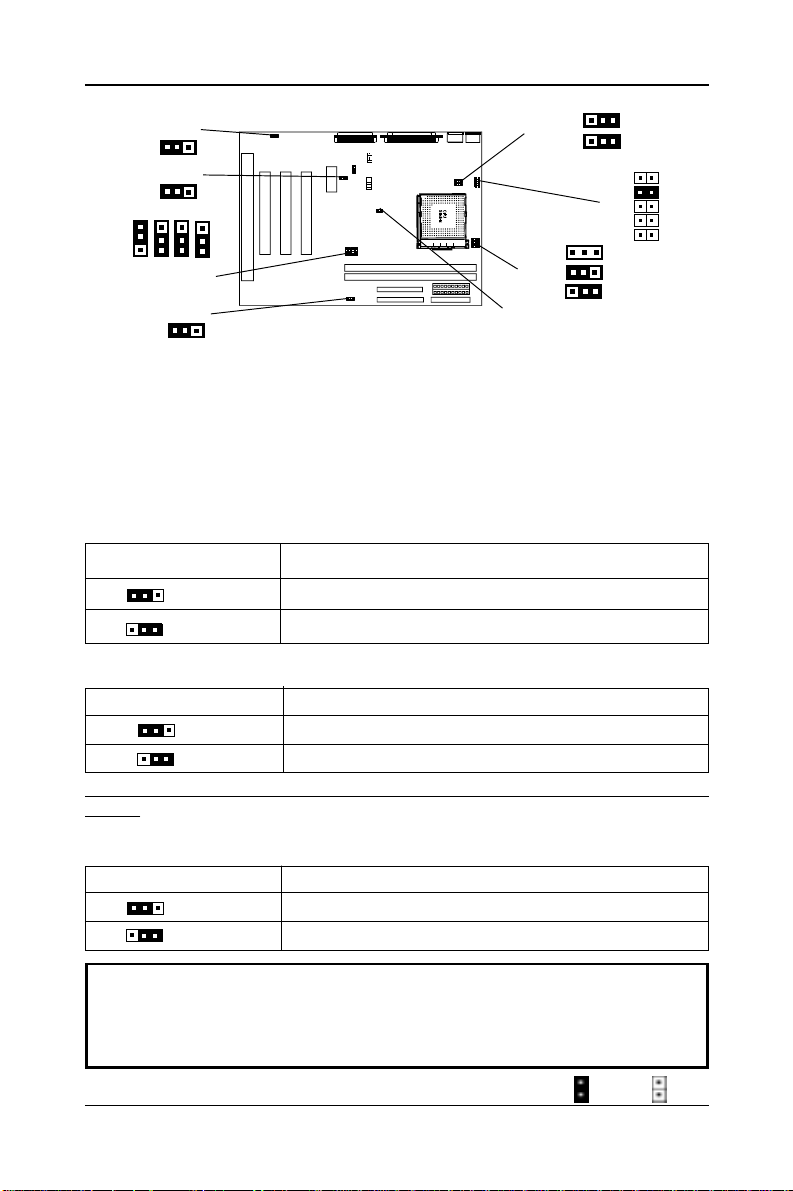
JP10 - System Memory Tuning Jumper
In order to cope with different type of DIMM memory in the market, a system
MEMORY TUNING jumper is provided.
In case of any power up problem due to the DIMM MEMORY, you can close the
jumper and try again.
If no problem is found, the jumper should be kept DEFAULT (OPEN).
JP31 - CMOS Clear
JP31 CMOS
1
(1-2)* Normal operation*
(2-3) Clear
1
9
JP36 - BIOS Program Voltage / BIOS Select
JP36 Selection
1
(1-2) INTEL/MX (2MB)
1
(2-3) A TMEL/SST/Winbond (2MB)
JP36 is pre-installed in the factory. They should NOT be altered by the
users.
JP41 - Selection for on Board AC97 or AMR AC97 Sound
JP41 Selection
1
(1-2)* on Board AC97 Sound*
1
(2-3) AMR AC97 Sound
Warning:
Before handling the motherboard from its original package, please
ensure that there is no static electricity on your body. Otherwise
it may cause damage to the integrated circuits on the motherboard.
* = Default setting.
Close Open
Hardware Setup
Page 10
10
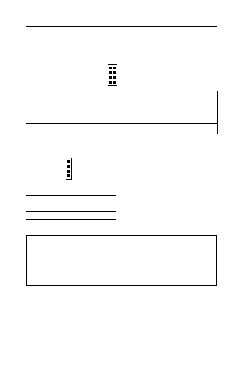
Pin List of Special Connectors:
1. CN7: USB connector
12
78
1 USB-VCC 2 USB-GND
3 USB DT2- 4 USB DT3+
5 USB DT2+ 6 USB DT37 USB-GND 8 USB-VCC
2. CN23: CD-IN
1
4
1 GND
2 CD-L
3 GND
4 CD-R
Warning:
Power on after Power-Fail
This new feature is enabled in this system, i.e. once plugging-in
the AC-power, the system will start-up automatically. Please install
all the components/devices into the system before plugging in the
AC-power plug.
Technical Reference Booklet
Page 11

11
Memory Configuration
The memory combinations. The motherboard will support Extended Data Output
(EDO), Burst Extended Data Output (BEDO) and Synchronous DRAM (SDRAM)
DIMMs.
DIMM Configurations
DIMM 1 DIMM 2 Total
Empty 8MB 8MB
Empty 16MB 16MB
Empty 32MB 32MB
Empty 64MB 64MB
Empty 128MB 128MB
8MB Empty 8MB
8MB 8MB 16MB
8MB 16MB 24MB
8MB 32MB 40MB
8MB 64MB 72MB
8MB 128MB 136MB
16MB Empty 16MB
16MB 8MB 24MB
16MB 16MB 32MB
16MB 32MB 48MB
16MB 64MB 80MB
16MB 128MB 144MB
DIMM 1 DIMM 2 Total
32MB Empty 32MB
32MB 8MB 40MB
32MB 16MB 48MB
32MB 32MB 64MB
32MB 64MB 96MB
32MB 128MB 160MB
64MB Empty 64MB
64MB 8MB 72MB
64MB 16MB 80MB
64MB 32MB 96MB
64MB 64MB 128MB
64MB 128MB 192MB
128MB Empty 128MB
128MB 8MB 136MB
128MB 16MB 144MB
128MB 32MB 160MB
128MB 64MB 192MB
128MB 128MB 256MB
Installation
Installing a DRAM Module
To install a DRAM module,
• Determine the desired amount of memory and acquire the necessary
DRAM modules.
• Note that a DRAM module has a polarity notch at one end so that it
fits into a socket only one way. Hold the module by the edges. Do not
touch the shiny contacts.
• Align the DRAM module edge connector with the slot at the center of the
socket.
• Position the DRAM module to the left of the socket and press the DRAM
module edge connector firmly into the socket.
If you have misaligned or only partially seated the module, remove the
DRAM module gently and reinstall it.
Warning:
Turn system power off before installing and removing any device,
otherwise you’ll cause the system damage.
Hardware Setup
Page 12

12
Installing the Processor
For easy installation of the CPU, it is recommended that you
remove all Cards in PCI slots first.
• Unpack the CPU and identify the pin 1 corner of the CPU.
• Match pin 1 of the CPU with pin 1 of the CPU socket. The pin 1 corner of
the CPU socket is designated by a small triangle printed on the motherboard.
• Carefully insert the CPU into the CPU socket and move the metal arm
downward to replace it in its original position. Change any jumper settings
as detailed in the manual.
The small circle marked on the top of the CPU designates the pin 1 corner.
If a heat sink is attached and covers the top of the CPU, identify the pin 1
corner by turning the CPU over. Locate the small gold finger that extends
from one corner of the large central square portion of the CPU. The gold
finger points towards pin 1, which is also uniquely identified by a square pad.
Positioning the CPU incorrectly in the socket can permanently damage
the CPU and the computer when you turn on the system.
Warning:
There is a fan attached the CPU to prevent the overheating, please
ensure that the fan can operate. Otherwise the CPU can overheat
and cause damage to both CPU and motherboard.
Technical Reference Booklet
Page 13

13
BIOS SETUP
This chapter discusses Award’s Setup Program built into the ROM BIOS. The
Setup Program allows users to modify the basic system configuration. This
special information is then stored in battery-backed RAM, which retains the
setup information when the power is turned off.
Starting Setup
The Award BIOS is immediately activated when you turn on the computer. The
BIOS reads the system information contained in the CMOS and begins the
process of checking out the system and configuring it. When it finishes, the
BIOS will seek an operating system on one of the disks and then launch and
turn control over to the operating system.
While the BIOS is in control, the Setup Program can be activated :
1. By pressing <Del> immediately after switching the system on, or
2. By pressing the <Del> key when the following message appears briefly at
the bottom of the screen during the POST (Power On Self Test )
Press DEL to enter SETUP
If the message disappears before you can respond and you still wish to enter
Setup, restart the system to try again by turning it OFF then ON or pressing the
“RESET” button on the system case. You may also restart by simultaneously
pressing the <Ctrl>, <Alt>, and <Delete> keys. If you do not press the keys at
the correct time and the system does not reset, an error message will be
displayed and you will again be asked to ...
PRESS F1 TO CONTINUE, DEL TO ENTER SETUP
Getting Help
Press F1 to pop up a small help window that describes the appropriate keys to
use and the possible selections for the highlighted item. To exit the Help
Window press <Esc> or the F1 key again.
In Case of Problems
If, after making and saving system changes with the Setup Program, you
discover that your computer does not reset, use the Award BIOS defaults to
override the CMOS settings.
Main Menu
Once you enter the Award BIOS CMOS Setup Utility , the Main Menu will appear
on the screen. The Main Menu allows you to select from various setup functions
and two exit choices. Use the arrow keys to select among the items and press
<Enter> to accept and enter the sub-menu.
BIOS Setup
Page 14

14
ROM PCI/ISA BIOS
CMOS SETUP UTILITY
AWARD SOFTWARE. INC.
STANDARD CMOS SETUP SYSTEM MONITOR DEVICE
BIOS FEATURES SETUP INTEGRATED PERIPHERALS
CHIPSET FEATURES SETUP SUPERVISOR PASSWORD
POWER MANAGEMENT SETUP USER PASSWORD
PNP/PCI CONFIGURATION IDE HDD AUTO DETECTION
LOAD BIOS DEFAULTS SAVE & EXIT SETUP
LOAD SETUP DEFAULTS EXIT WITHOUT SAVING
Esc : Quit éêèç : Select Item
F10 : Save & Exit Setup (Shift) F2 : Change Color
Time. Date. Hard Disk Type
(Note : The figures of BIOS Setup Menu included here only show a typical
case, and may not be exactly the same as the one on your unit.)
Note that a brief description of each highlighted item will appear at the bottom
of the screen.
Standard This setup page includes all the items of Award™ special
CMOS Setup standard features.
BIOS Features This setup page includes all the items of Award™ special
Setup enhanced features.
Chipset This setup page includes all the items of chipset special
Features Setup features.
Power This entry only appears if your system supports Power
Management Management “Green PC” standards.
Setup
PNP / PCI This entry appears if your system supports PNP/PCI.
Configuration
Load BIOS The BIOS defaults have been set by the manufacturer and
Defaults represent settings which provide the minimum requirements
for your system to operate.
Load Setup The chipset defaults are settings which provide for maximum
Defaults system performance. While Award has designed the custom
BIOS to maximize performance, the manufacturer has the
right to change these defaults to meet its needs.
System Monitor In this feature setting, you can observe the speed of CPU fan
Device and actual V oltage for 2.5V , 3.3V , CPU Core V oltage, +5V and
+12V .
Technical Reference Booklet
Page 15

15
Integrated This section page includes all the items of IDE hard drive and
Peripherals Programmed Input / Output features.
Supervisor / Changes, sets, or disables password. It allows you to limit
User Password access to the system and the Setup Program.
Setting
IDE HDD Auto Automatically detects and configures the hard disk parameters.
Detection The Award BIOS includes this ability in the event you are
uncertain of your hard disk’s parameters.
Save & Exit Saves value changes to CMOS and exits setup.
Setup
Exit Without Abandons all CMOS value changes and exits setup.
Save
Standard CMOS Setup
The items in Standard CMOS Setup Menu are divided into 10 categories. Each
category includes one or more setup items. Use the arrow keys to highlight the
item and then use the <PgUp> or <PgDn> key to select the desired value in
each item.
ROM PCI/ISA BIOS
STANDARD CMOS SETUP
AWARD SOFTWARE. INC.
Date (mm:dd:yy) : Thu, Jan 23 1997
Time (hh:mm:ss) : 00:00:00
HARD DISKS TYPE SIZE CYLS. HEADS PRECOMPLANDZ SECTORS Mode
Primary Master : None 0 0 0 0 0 0 --Primary Slave : None 0 0 0 0 0 0 --Secondary Master : None 0 0 0 0 0 0 --Secondary Slave : None 0 0 0 0 0 0 ---
Drive A : 1.44M, 3.5 in Base Memory : 640K
Drive B : None Extended Memory : 15360K
Video : EGA/VGA Other Memory : 384K
Halt on : All Errors T otal Memory : 16384K
Esc : Quit éêèç: Select Item PU/PD/+/- : Modify
F1 : Help (Shift) F2 : Change Color
(Note : The figures of BIOS Setup Menu included here only show a typical
case, and may not be exactly the same as the one on your unit.)
Date The date format is <day-of-the-week>. <day> <month> <year>.
Press <F3> to display the calendar.
Time The time format is <hour> <Minute> <second> displayed in
24-hour military-time clock. For example, 1 p. m. is displayed
as 13:00:00.
BIOS Setup
Page 16

16
Primary These categories identify the types of the two channels that
Master/Primary have been installed in the computer. There are 45 predefined
Slave/Secondary types and one user definable types in BIOS. Type 1 to Type 45 are
Master/Secondary predefined. Type “user” is user-definable.
Slave
Press PgUp or PgDn to select a numbered hard disk type
or type the number and press <Enter>. Note that the
specifications of your drive must match with those of the
drive table. The hard disk will not work properly if you enter
improper information for this category . If your hard disk drive
type is not matched or listed, you can select Type “User” to
define your own drive type manually.
If you select Type “User”, you will need to know the
information listed below. Enter the information directly from
the keyboard and press <Enter>. This information should
be included in the documentation from your hard disk vendor
or the system manufacturer.
If the controller of the HDD interface is ESDI, the selection
shall be “Type1”.
If the controller of the HDD interface is SCSI, the selection
shall be “None” .
If you select Type “Auto”, the BIOS will auto-detect the HDD
and CD-ROM drive at the POST stage and show the IDE for
the HDD and CD-ROM drive.
TYPE -Drive type
CYLS -Number of cylinders
HEADS -Number of heads
PRECOMP -Write precom
LANDZONE -Landing zone
SECTORS -Number of sectors
MODE -Mode type
If a hard disk has not been installed, select NONE and
press <Enter> .
Drive A Type / This category identifies the types of floppy disk drive A or
Drive B Ty pe drive B that has been installed in the computer.
Video This category selects the type of video adapter used for the
primary system monitor. Although secondary monitors are
supported, you do not have to select them in Setup.
BIOS Features Setup
This section allows you to configure your system for basic operation. You have
the opportunity to select the system’s default speed, boot-up sequence,
keyboard operation, shadowing and security.
Technical Reference Booklet
Page 17

17
Chipset Features Setup
The Chipset Features Setup option is used to change the values of the chipset
registers. These registers control most of the system options in the computer.
This section allows you to configure the system based on the specific features
of the installed chipset. This chipset manages bus speeds and access to
system memory resources, such as DRAM and the external cache. It must be
stated that these items should not be altered. The default settings have been
chosen because they provide the best operating conditions for your system.
Power Management Setup
The Power Management Setup Menu allows you to configure your system to
most save energy while operating in a manner consistent with your own style
of computer use .
PNP/PCI Configuration
This section describes how to configure the PCI bus system. This section
covers some very technical items and it is recommended that only experienced
users should make any changes to the default settings.
Integrated Peripherals
The Integrated Peripherals Setup allows the user to configure the onboard
IDE controller, floppy disk controller, the printer port and the serial ports.
Supervisor/User Password Setting
Y ou can set either supervisor or user password, or both of them. The dif ference
between them are:
Supervisor Password : Y ou can enter the Setup Program and change
the options of the setup menus.
User Password : Y ou can enter the Setup Program but cannot
change the options of the setup menus.
When you select this function, the following message will appear at the center
of the screen to assist you in creating a password.
ENTER PASSWORD:
Type the password, up to eight characters in length, and press<Enter>. The
new password will clear the previously entered password from the CMOS
memory. You will be asked to confirm the password. Type the password again
and press <Enter>. You may also press <Esc> to abort the selection and
operate without a password.
To disable a password, just press <Enter> when you are prompted to enter the
password. A message will be displayed to confirm that the password is
disabled.
BIOS Setup
Page 18

18
PASSWORD DISABLED.
Once the password is disabled, the system will reset and you can enter the
Setup Program freely.
When a password is enabled, you will be prompted to enter it every time you try
to enter setup. This prevents an unauthorized person from changing any setting
of your system configuration.
In addition, when a password is enabled, you can require the BIOS to request
a password every time your system is rebooted. This would further prevent
unauthorized use of your computer.
The password requirement is defined by the Security Option of the BIOS
Features Setup Menu. If the Security Option is set to “System”, the password
will be required both at resetting and at entering setup. If the option is set to
“Setup”, the prompt only appears when you try to enter setup.
Flash Update Procedure
A program AWDFLASH.EXE is included in the utility diskette or CD. The user is
recommended to follow the procedure below to update the flash BIOS.
1. Create a DOS-bootable floppy diskette. Copy the new BIOS file (just obtained
or downloaded) and the utility program AWDFLASH.EXE to the diskette.
2. Allow the PC system to boot from the DOS diskette.
3. At the DOS prompt, key in
AWDFLASH
and hit <ENTER>
4. Enter the file name of the new BIOS.
5. The question: “Do you want to save file?” is displayed.
Key in “N” if there is no need to save the existing BIOS content..
Key in “Y” if a backup copy of the existing BIOS is needed.
(A file name has to be assigned to the existing BIOS binary file.)
6. The question : “Are you sure to program?” is displayed.
Key in “Y”
7. Wait until the flash-update is completed.
8. Power down the PC system.
9. Restart the PC.
Warning:
1. If the flash memory writer utility was not able to successfully
update a complete BIOS file, the system may not boot up.
2. Make sure that the BIOS file is available for this motherboard.
3. If you encounter problem while updating the new BIOS, DO NOT
turn off your PC since this might prevent the system from booting
up. Repeat the process, if the problem still persist, use the original
BIOS file you saved to disk above to update. If it failed, you need
service.
Technical Reference Booklet
Page 19
19
APPENDIX - Technical Reference
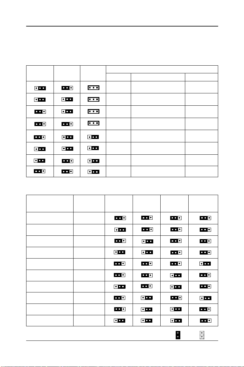
CPU to Bus Frequency Ratio (JP1, JP2, JP6)
JP1, JP2 and JP6 are used in combination to decide the ratio of the internal frequency
of the CPU to the bus clock.
JP1 JP2 JP6 CPU to Bus Frequency Ratio
AMD K6 Pentium MMX/6x86MX 6x86L
1
1
1
3x 3x 3x
1
1
1
1
1
1
1
1
1
1
1
1
1
1
1
1
1
1
1
1
1
2.5x 2.5x 2.5x
2x 2x 2x
3.5x 3.5x 3.5x
4x --- ---
4.5x --- - -5x --- ---
5.5x --- - --
CPU External Clock (BUS) Frequency (JP3, JP4, JP5, JP8)
JP3, JP4, JP5 and JP8 for the different CPU speed configuration.
CPU, SDRAM PCI JP3 JP4 JP5 JP8
(MHz) (MHz)
60 30
66.8 33.4
70 35
75 25
75 37.5
80 26.6
83.3 27.77
83.3 41.65
95.25 31.75
100.2 33.3
1
1
1
1
1
1
1
1
1
1
1
1
1
1
11
1
1
1
1
1
1
1
1
1
1
1
1
1
1
1
1
1
1
1
1
1
1
1
1
Close Open
APPENDIX - T echnical Reference
Page 20
20
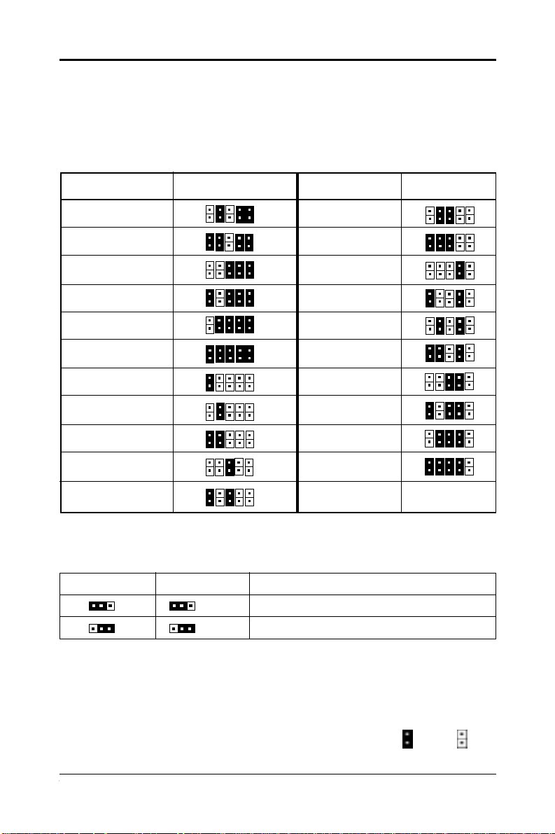
CPU Core Voltage (JP11)
This motherboard utilize switching control power. Support a wide CPU Core Voltage
from 1.8V to 3.5V. You can use it for further CPUs. Please correctly set jumpers refer
to your CPU Marking, CPU Core Voltage setting is as below.
Core Voltage JP11 Core Voltage JP11
1.8V 2.6V
1.85V 2.7V
1.9V 2.8V
1.95V 2.9V
2.0V 3.0V
2.05V 3.1V
2.1V 3.2V
2.2V 3.3V
2.3V 3.4V
2.4V 3.5V
2.5V
2
1
2
1
2
1
2
1
2
1
2
1
2
1
2
1
2
1
2
1
2
1
2
1
2
1
2
1
2
1
2
1
2
1
2
1
2
1
2
1
2
1
JP39, JP40 - CPU Power Supply (for single voltage or double
voltage CPU)
JP39 JP40 CPU
1
(1-2) (1-2) for single voltage
1
(2-3) (2-3) for double voltage
Double Voltage: All power PINs of CPU are divided into two parts, one part is provided
Single Voltage: All power PINs of CPU are provided with only one kind of voltage.
Technical Reference Booklet91-8897-00
1
1
with the voltage called VI/O, another part is provided with the voltage
called Vcore.
Close Open
 Loading...