


PC Engines
WRAP router platform
Versions WRAP.1C / .1D / .1E, WRAP.2B / .2C / .2D / .2E

WRAP router platform 2 2/13/2007
2003-2006 PC Engines GmbH. All rights reserved.
PC Engines GmbH
pdornier@pcengines.ch
www.pcengines.ch
tinyBIOS and PC Engines are trademarks of PC Engines GmbH.
All other marks and brands are property of their respective owners.

WRAP router platform 3 2/13/2007
Table of contents
Federal Communications Commission Statement 4
CE Declaration of Conformity 4
Compliance information 4
Recycling / disposal 5
Introduction / features 6
OEM options 6
Technical data 8
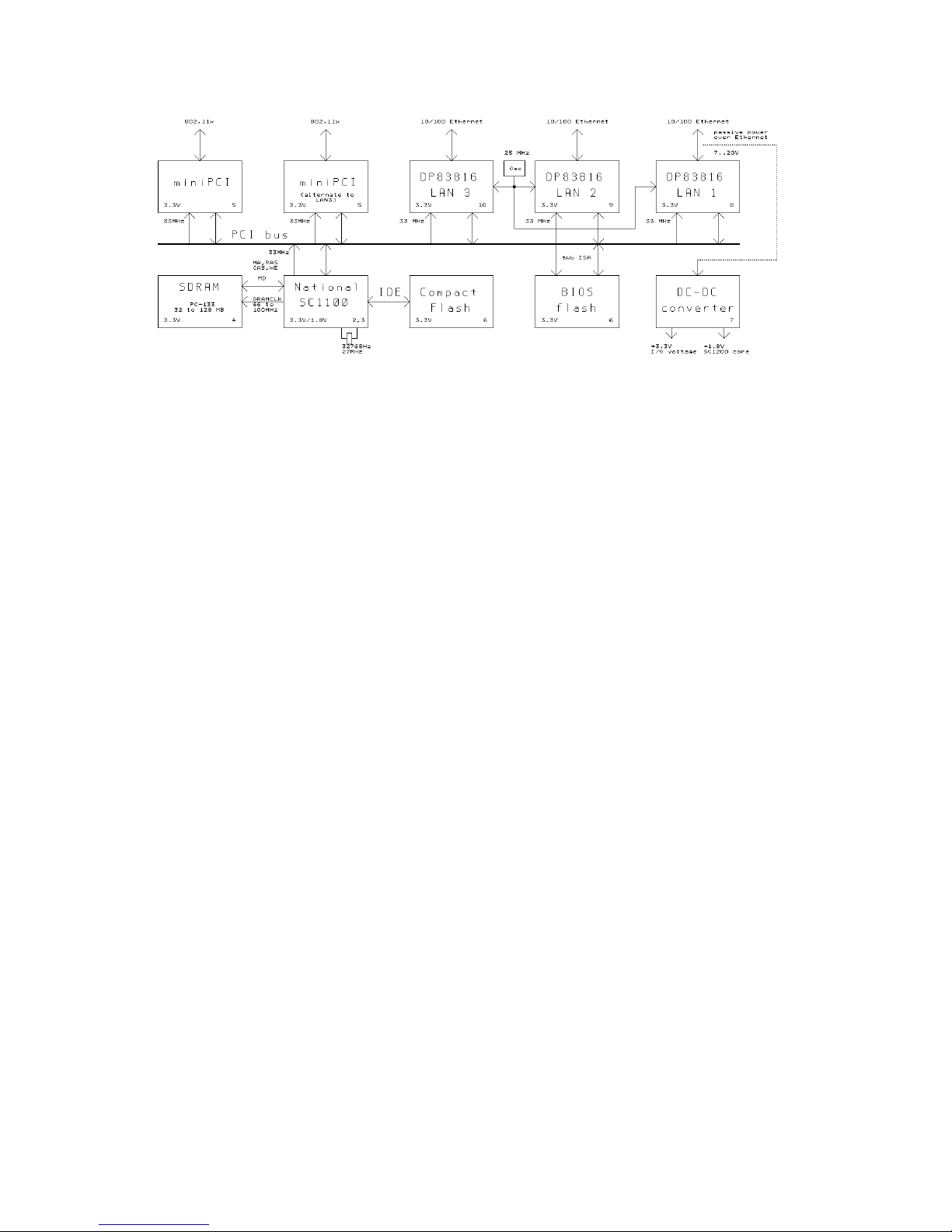
Block diagram 8
Getting started… 9
Setup options 9
CompactFlash partitioning 10
Thermal sensor 10
Front panel LEDs and switch 10
Format of X-Modem upload files 11
Power over Ethernet 11
Real-Time Clock 11
Known issues 11
WRAP.1D / WRAP.1E revision changes 12
WRAP.1C / WRAP.1D revision changes 12
WRAP.2B / WRAP.2C revision changes 12
Support 12
FreeBSD 13
Linux 14
MikroTik RouterOS 15
NetBSD 16
OpenBSD 17
RxDOS 18
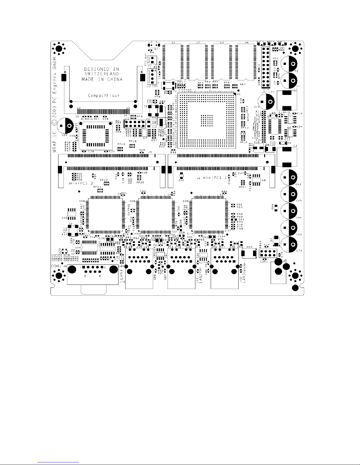
WRAP.1C connector pinouts 19
WRAP.1C mechanical dimensions 23
WRAP.2B connector pinouts 24
WRAP.2B mechanical dimensions 25
Resources 27

WRAP router platform 4 2/13/2007
Federal Communications Commission Statement
This device complies with Part 15 of the FCC Rules. Operation is subject to the following two
conditions: (1) this device may not cause harmful interference, and (2) this device must accept any
interference received, including interference that may cause undesired operation.
This equipment has been tested and found to comply with the limits for a Class B digital device,
pursuant to Part 15 of the FCC Rules. These limits are designed to provide reasonable protection
against harmful interference in a residential installation. This equipment generates, uses and can
radiate radio energy. If this equipment is not installed and used in accordance with the
manufacturer’s instructions, it may cause harmful interference to radio communications. However,
there is no guarantee that interference will not occur in a particular installation. If this equipment
does cause harmful interference to radio or television reception, which can be determined by
turning the equipment off and on, the user is encouraged to correct the interference by one or more
of the following measures:
• Reorient or relocate the receiving antenna.
• Increase the separation between the equipment and receiver.
• Connect the equipment to an outlet on a circuit different from that to which the receiver is
connected.
• Consult the dealer or an experienced radio/TV technician for help.
This board is designed for installation in a shielded enclosure (metal or plastic with conductive
coating). Shielded cables are required on LAN and serial ports to assure compliance with FCC
regulations.
A copy of the test report will be provided on request.
CE Declaration of Conformity
We, PC Engines GmbH, declare that WRAP.1C / WRAP.1D, when installed in the PC Engines
metal enclosure, is in conformance with:
- EN 61000-6-3 and EN 61000-6-4 (EMI emissions, residential and industrial)
- EN 61000-6-1 and EN 61000-6-2 (ESD, susceptibility, residential and industrial)
A copy of the test report will be provided on request.
Compliance information
For FCC, WRAP has been tested as a CPU board, installed in an enclosure, with the top cover
removed. No further testing should be required if the board is used with other FCC tested modular
components. Please see http://www.fcc.gov/oet/ for more details. The responsible party for FCC is
the importer.
Testing for CE mark must be done at the level of the complete product, possibly including the
wireless cards. Please contact PC Engines for assistance and documentation.
For satisfactory resistance to electrostatic discharge events (ESD), the WRAP board should be
grounded (e.g. through the mounting holes, or the serial port connector).

WRAP router platform 5 2/13/2007
Recycling / disposal
Do not discard electronic products in household trash !
All waste electronics equipment should be recycled properly. Actual procedures depend on your
country.
Information for the recycler:
PC Engines enclosures are made of Aluminum.
Batteries, if present, should be cut off or removed from the socket and recycled separately.
PCB boards may include SnPb (tin-lead) solder and should be recycled properly.

WRAP router platform 6 2/13/2007
Introduction / features
WRAP is a small single board computer optimized for wireless access and network routing
applications.
• National SC1100 CPU, 233 or 266 MHz 5x86 CPU, 16KB cache
• 2 or 3 Ethernet channels (National DP83816); 1 channel on WRAP.2B
• 2 or 1 miniPCI sockets for 802.11 wireless cards and other expansion
• 64 MB SDRAM, 64 bit wide for high memory bandwidth
• 128 KB flash for tinyBIOS system BIOS.
• CompactFlash header for user’s operating system and application
• 7 to 18V DC supply through DC jack or passive power over LAN 1 connector
• 1 serial port (DB9 male)
• Watchdog timer built into SC1100 CPU
• LM77 thermal monitor (not on WRAP.2D or WRAP.2E)
• Header for I2C bus (can be used for front panel interface)
• Header for LPC bus (can be used for I/O expansion)
• 3 LEDs and 1 pushbutton switch, freely programmable.
OEM options
The following accessories are available:
• CompactFlash cards
• Power over Ethernet injector POE.1A
The following options can be configured for larger orders:
• DRAM size (32 MB, 64 MB, 128 MB)
• 1 or 3 Ethernet channels (limit to 1 miniPCI if 3 Ethernet)
• 1 or 0 Serial ports
• Delete front panel LEDs and switch
• Custom BIOS adaptations as needed
• Full BIOS source can be licensed for adaptation by OEM
• USB port (no power over Ethernet, 5V DC supply only)
• Full custom board versions.
WRAP router platform 7 2/13/2007
WRAP router platform 8 2/13/2007
Technical data
Power supply +12V DC, ~ 0.25A halt, ~ 0.4A active (excluding miniPCI cards)
recommended range +7 to +18V DC, TVS limit at 20V !
Center pin = positive, sleeve = ground.
Temperature range 0 to 50°C. The temperature range may be extended by using a CPU heat sink
(not included), and reducing CPU frequency to 233 MHz.
Dimensions WRAP.1C = 6 x 6” (152.4 x 152.4 mm)
WRAP.2B = 3.937” x 6.3” (100 x 160 mm)
Block diagram
Full schematics are available on the PC Engines web site.
WRAP router platform 9 2/13/2007
Getting started…
- Connect a DC power supply to the DC jack J9. 2.1 mm center pin = positive, sleeve = ground.
Supply voltage should be between 7V and 18V (TVS on the input starts clamping around 20V).
Power supply should be able to supply at least 7.5W, 15W suggested for more margin and
reliability.
- Connect the serial console using a DB9 null modem cable. Default serial port parameters are
38400 8N1. Do NOT use a 1:1 connected serial cable, as the serial port may get damaged.
- While power is off, insert CompactFlash card with your operating system and application in
CompactFlash header J4. Hot swap of CompactFlash cards is not supported !
- Power on…
You should see tinyBIOS startup messages, memory size, CF disk geometry on the serial console.
Setup options
Configure your terminal emulator for 38400 8N1 (default baud rate), no handshake. To enter
setup, type S during the memory test. You should see somethink like the following:
PC Engines WRAP platform
tinyBIOS V1.4a (C)1997-2003 PC Engines
640 KB Base Memory
64512 KB Extended Memory
01F0 Master 848A HYPERSTONE FLASH DISK
Phys C/H/S 497/4/32 Log C/H/S 31/32/63
WRAP setup
(9) 9600 baud *3* 38400 baud
(C) CHS mode *L* LBA mode
(X) Xmodem upload (Q) Quit

WRAP router platform 10 2/13/2007
The active options are marked by *, e.g. *3* means 38400 baud mode is active. Setup options are
stored in a 4KB block of flash, not in RTC CMOS. The following options can be set:
- Baud rate 9600 baud (9) or 38400 baud (3). Default is 38400 baud.
- CompactFlash translation mode CHS (C) or LBA (L). Default is CHS.
- XMODEM upload of new firmware (X). Start transmission when prompted. 128 byte and 1024
byte packet sizes can be accepted, CRC mode only. Checksum mode is not supported as it is
considered too risky for firmware upgrade.
The actual flash update algorithm is included in the uploaded file. Flash programming takes
about two seconds. If power fails during this time, the BIOS chip will need to be reprogrammed
through other means.
- Quit (Q) – setup will ask whether it should write the new settings to flash (Y) or not (N).
OEMs can request a utility to insert their own sign-on message into the BIOS binary.
CompactFlash partitioning
tinyBIOS is set up to configure the CF card in CHS mode. CHS mode is dependent on the
geometry of the CF card, but is more likely to work consistently across systems.
If using LBA mode, please make sure that the disk geometry on the system where the card is
initialized matches that shown by the WRAP BIOS during startup. A mismatch will cause problems.
Another possible issue are cards with IDE DMA support – the DMA signals are a fairly recent
addition to the CF spec, and are not supported by WRAP. If you experience problems with IDE
access later in the boot process, try to disable IDE DMA in your operating system.
Thermal sensor
The thermal sensor will reset the system when the temperature exceeds a critical level (power on
default = 80C). Reset will be released when the temperature goes back down.
The LM77 thermal sensor sits on the secondary I2C bus, at address 90h. DOS based sample code is
available on request. National also has a Linux driver for the I2C, but this probably needs some
work.
Front panel LEDs and switch
LED1 (D3) GPIO2 write I/O port [GPIOBASE] bit 2 0 = light
LED2 (D2) GPIO3 write I/O port [GPIOBASE] bit 3 0 = light
LED3 (D1) GPIO18 write I/O port [GPIOBASE] bit 18 0 = light
Switch (S1) GPIO40 read I/O port [GPIOBASE+20] bit 8 0 = pressed
With tinyBIOS, GPIOBASE is 0F400h. If you would like to write a more generic driver, use the
SC1100 I/O base registers to determine GPIOBASE.

WRAP router platform 11 2/13/2007
Format of X-Modem upload files
The uploaded file is stored starting at offset 1000:0. The first two bytes are a signature, and should
be TB. Setup will do a far call to 1000:2 if the signature is detected. ES:DI points to the end of the
uploaded file in memory.
Power over Ethernet
WRAP implements a passive power over Ethernet scheme, using the unused pairs of LAN1 for
power. Power can be injected using a passive POE splitter such as PC Engines POE.1A.
When power is fed in through POE, it is possible to “steal” unregulated power through the DC jack.
Please note that this port is not fused. The POE input diode is rated for a current of 3A. Please
keep in mind that any EMI energy injected on this port will go out through the Ethernet cable
without further filtering.
Real-Time Clock
WRAP does not include a battery backup for the real-time clock (RTC).
The A3 stepping of the SC1100 CPU had a problem with the 32768 Hz oscillator, leading to
potential RTC inaccuracy. This version also was sensitive to ESD on the battery voltage pin.
A backup battery can be connected as follows:
WRAP.1C / .1D: Add a 100 ohm, 0603 resistor in location R5, replace the 0 ohm resistor in location
C105 (bottom side) with a 0.1uF 0603 capacitor, install a 2 pin header in location J1. Connect 3V
Lithium battery to J1, observing the polarity marks.
WRAP.2B / .2C: Connect 3V battery to J7 pin 7 (positive) and pin 8 (negative).
SC1100 is specified for a battery voltage of 2.4 to 3.6V, drain current 7 to 30 µA. At 30µA, a
CR2032 Lithium coin cell will last only about a year – please consider a larger CR123 Lithium (often
used in cameras).
Known issues
Reset may not work reliably on very short power interruptions. Please make sure that power remains
off for at least a second.

WRAP router platform 12 2/13/2007
WRAP.1D / WRAP.1E revision changes
The following changes were made going from revision 1D to revision 1E:
pd 050101 3 Change R97 to 1.5K (ECN009).
6 Add optional buzzer (e.g. Hycom HY-05) in place of C22.
6 Add optional soldered battery.
6 Add IDE DMA support.
6 Change to TSOP flash (to make space for soldered
battery + commonality with WRAP.2C).
7 Add 2.2nF capacitor on OVERTMP# net (ECN009).
7 Delete MIC8115 alternative reset.
7 Add BAS40-06 dual diode as alternative to MBR0520L.
PCB Reroute OVERTMP# to avoid surge coupling.
PCB Change 4.7uF capacitors to 0805 package.
WRAP.1C / WRAP.1D revision changes
The following changes were made going from revision 1C (China) to revision 1D (Taiwan):
pd 040512 5 Change J5 miniPCI (optional) to REQ3, GNT3.
Change J6 miniPCI (always populated) to REQ0, GNT0.
6 Serial port -> disable auto power down
(ONLINE# = FORCEON high).
10 Change LAN3 to REQ3, GNT3.
PCB Change silk screen to "Assembled in Taiwan".
WRAP.2B / WRAP.2C revision changes
The following changes were made going from revision 2B (China) to revision 2C (Taiwan):
pd 040520 5 Change miniPCI socket from REQ3/GNT3 -> REQ2 / GNT2.
pd 040512 PCB Change silk screen to "Assembled in Taiwan".
Support
Please email pdornier@pcengines.ch.

WRAP router platform 13 2/13/2007
FreeBSD
A ready-to-boot firewall configuration is available at http://www.m0n0.ch/wall/
The default FreeBSD boot sector expects a keyboard controller to be present. This will hang on the
WRAP board.
Modify src/sys/boot/i386/boot2/boot1.s to skip this routine (e.g. patch in a ret instruction).
//
// Enable A20 so we can access memory above 1 meg.
//
seta20: cli // Disable interrupts
seta20.1: inb $0x64,%al // Get status
testb $0x2,%al // Busy?
jnz seta20.1 // Yes
movb $0xd1,%al // Command: Write
outb %al,$0x64 // output port
seta20.2: inb $0x64,%al // Get status
testb $0x2,%al // Busy?
jnz seta20.2 // Yes
movb $0xdf,%al // Enable
outb %al,$0x60 // A20
sti // Enable interrupts
retw // To caller
(courtesy of Larry Baird) The following lines added to cpu_reset_real() in
sys/i386/i386/vm_machdep.c will allow a WRAP board to reboot when running freeBSD:
outl( 0xCF8, 0x80009044UL ); // reset control (SC1100 data
// sheet, page 170
outb( 0xCFC, 0x0F ); // system wide reset
WRAP support is included in FreeBSD release 5.3 – disable KBD and VGA and recompile the
kernel.

WRAP router platform 14 2/13/2007
Linux
The kernel should be configured not to look for a keyboard controller to avoid error messages.
A driver for the SC1100 watchdog can be found at http://www.conman.org/software/wd1100 , or
at http://www.sk-tech.net/support/soekris.html .
(courtesy of Erich Titl) Linux needs a patch to pc_keyb.c to avoid the keyboard jammed message at
start up. The patch is written by Randy Dunlap and is somewhat difficult to find. A copy can be
found at http://cvs.sourceforge.net/viewcvs.py/leaf/devel/etitl/kernel/kbc_option_2420.patch .
Old versions of the GRUB boot loader has broken A20 gate code, and may have problems in 8250
/ 16550 detection. The UART has the FIFO, detection can be skipped.
Another way (A.J.T. Toorman): change pc_keyb.c (in Linux kernel file /drivers/char) file as follows:
#define kbd_controller_present() 0
Reboot through the non-existing keyboard controller will not work. For LRP / Bering, edit
syslinux.cfg:
default linux rw reboot=bios initrd=initrd.lrp init=/linuxrc ...
Direct hardware reset:
mov eax,080009044h ;reset control,
mov dx,0cf8h ;SC1100 data sheet page 170
out dx,eax
mov al,0f ;system wide reset
mov dl,0fch
out dx,al
LED access (contributed by Josef Liška, used LRP Bering 2.2.2):
#led3on
echo "A" | dd of=/dev/port bs=1 count=1 seek=62466
#led3off
echo "L" | dd of=/dev/port bs=1 count=1 seek=62466
#led12on
echo "A" | dd of=/dev/port bs=1 count=1 seek=62464
#led12off
echo "L" | dd of=/dev/port bs=1 count=1 seek=62464
#led1on 2off
echo "H" | dd of=/dev/port bs=1 count=1 seek=62464
#led 1off 2on
echo "D" | dd of=/dev/port bs=1 count=1 seek=62464
I2C: The stock linux kernel driver (scx200_acb) looks for the two ACCESS.bus interfaces at
addresses 0x820 and 0x840, while tinyBIOS configures then at 0x810 and 0x820. Load the driver as
follows:
modprobe scx200_acb base=0x810,0x820

WRAP router platform 15 2/13/2007
MikroTik RouterOS
Please request the latest BIOS version from PC Engines when using RouterOS.
RouterOS is very picky about CompactFlash cards, do extensive torture tests including repeated
configuration and shutdown cycles before qualifying for production use.
WRAP does not include a keyboard controller. To ensure clean restart, please install the package
routerboard.npk
from
http://www.mikrotik.com/download.html#v2 -> all_packages.zip
The package is designed for MikroTik’s RouterBOARD, but will also work for WRAP. Source:
MikroTik technical support.
RouterBOARD, RouterOS and MikroTik are trademarks of MikroTik.

WRAP router platform 16 2/13/2007
NetBSD
For USB support, please add the following to the kernel config file:
options PCIBIOS # PCI BIOS support
options PCIBIOSVERBOSE # PCI BIOS verbose info
options PCIBIOS_ADDR_FIXUP # fixup PCI I/O addresses
options PCIBIOS_BUS_FIXUP # fixup PCI bus numbering
options PCIBIOS_INTR_FIXUP # fixup PCI interrupt routing

WRAP router platform 17 2/13/2007
OpenBSD
WRAP support is included in OpenBSD 3.5. To read and write the GPIO pins, the gpioctl program
included with this package can be used:
Quick start for the PC Engines WRAP.1C users:
# gpioctl 40
This will read the state of the button (0 means pressed).
# gpioctl -c 2 pp out
This will turn the first led on, to turn off write 1 to the pin,
it's reversed. For the second and the third leds use pins 3 and
18.
Even more WRAP support in OpenBSD 3.6:
• New gscpcib(4) driver for National Semiconductor Geode SC1100 PCI-ISA bridges.
• New iic(4) driver for Inter IC (I2C) master/slave buses.
• New lmtemp(4) driver for National Semiconductor LM75/LM77 temperature sensors.
• New gscsio(4) driver for National Semiconductor Geode SC1100 Super I/O chips.
• New gpio(4) driver and accompanying gpioctl(8) utility for supporting General Purpose
Input/Output.

WRAP router platform 18 2/13/2007
RxDOS
RxDOS is a free DOS-compatible operating system written by Michael Podanoffsky. RxDOS can be
used for functional testing.
RxDOS seems to be badly behaved on the serial console, though.
Full A386 source code and binary can be found at http://os.drake3d.com/
Recommended procedure to install on a CompactFlash card:
1. Select translation mode for the CF card to be LBA.
2. Clear partition sector using a disk editor if necessary.
3. Create partition with FDISK. If the CompactFlash card is drive C, make partition active.
4. Reboot, then FORMAT partition.
5. If the CompactFlash is drive D, use the partition editor EDPART (download from Simtel) to
make the partition active.
6. Modify mk_boot.bat (RxDOS bin directory) as needed, execute it:
makerxd_boot -1 -s d
copy ..\rxdosbio\rxdosbio.sys d:
copy ..\rxdos\rxdos.sys d:
copy ..\rxdoscmd\rxdoscmd.com d:
copy autobat d:\autoexec.bat

WRAP router platform 19 2/13/2007
WRAP.1C connector pinouts
J1 RTC battery
This connector is depopulated on current versions. Contact PC Engines for details if RTC is
required !
1 VBAT battery + (3V Lithium battery)
2 GND battery -
J2 LPC expansion
The LPC port can be used to connect a super I/O device, or for an alternate flash EPROM to start
with a corrupted or blank flash EPROM on board. These pins can also be reprogrammed as GPIO
(not tested): Clear PMR pin multiplex register (I/O 09030h) bit 14 and 16, then set correct GPIO
direction (input / output). Please see the SC1100 data sheet for details.
1 PCLK2 LPC clock (33 MHz)
2 GND ground
3 LAD0 LPC data 0 (GPIO32)
4 GND ground
5 LAD1 LPC data 1 (GPIO33)
6 GND ground
7 LAD2 LPC data 2 (GPIO34)
8 GND ground
9 LAD3 LPC data 3 (GPIO35)
10 GND ground
11 LFRAME# LPC frame (GPIO37)
12 GND ground
13 PCIRST# reset (active low)
14 NC reserved
15 LPCISP high to use LPC flash, low to use on-board flash, pulled low by resistor
16 NC reserved
17 GND ground
18 V3 +3.3V supply
19 SERIRQ serial interrupt (GPIO39)
20 LDRQ# LPC DMA request (GPIO36)
J3 I2C header
This header can be used to connect user specific hardware, e.g. a front panel microcontroller, or for
a licensing dongle.
1 +3.3V power supply
2 SCL1 I2C clock
3 SDA1 I2C data
4 GND ground
J4 CompactFlash
The CompactFlash card is used in True IDE mode. Hot insertion is not supported – please power
off the unit before inserting a CF card.
1 GND ground
2 D3 IDE data

WRAP router platform 20 2/13/2007
3 D4 IDE data
4 D5 IDE data
5 D6 IDE data
6 D7 IDE data
7 CS0# IDE decode (1F0..1F7)
8 A10 ground
9 ATASEL# ground to select true IDE mode
10 A9 ground
11 A8 ground
12 A7 ground
13 VCC +3.3V power supply
14 A6 ground
15 A5 ground
16 A4 ground
17 A3 ground
18 A2 IDE address
19 A1 IDE address
20 A0 IDE address
21 D0 IDE data
22 D1 IDE data
23 D2 IDE data
24 IO16# 16 bit decode, not connected
25 CD2# card detect, not connected
26 CD1# card detect. not connected
27 D11 IDE data
28 D12 IDE data
29 D13 IDE data
30 D14 IDE data
31 D15 IDE data
32 CS1# IDE decode (3F6..3F7)
33 VS1# not connected
34 IOR# IDE read strobe
35 IOW# IDE write strobe
36 WE# connected to +3.3V
37 IRQ IDE interrupt
38 VCC +3.3V power supply
39 CSEL# cable select, ground = master
40 VS2# not connected
41 RESET# IDE reset, active low
42 IORDY IDE ready
43 INPACK# not connected
44 REG# connected to +3.3V
45 DASP# pulled up
46 PDIAG# pulled up
47 D8 IDE data
48 D9 IDE data
49 D10 IDE data
50 GND ground
The CompactFlash specification can be found at www.compactflash.org.

WRAP router platform 21 2/13/2007
J5, J6 miniPCI sockets
These sockets implement the miniPCI interface.
Please note that the current available from the +5V supply is very limited, and generated very
inefficiently (linear regulator from input supply). +5V should be used as a bias voltage only, not to
power a wireless radio !
J8 Console serial port
The standard PC pinout is used. To connect to a PC, use a null modem or “Laplink” cable.
1 DCD data carrier detect (input)
2 RXD# receive data (input)
3 TXD# transmit data (output)
4 DTR data terminal ready (output)
5 GND ground
6 DSR data set ready (input)
7 RTS ready to send (output)
8 CTS clear to send (input)
9 RI ring indicator (input)
J9 DC power jack
This is a generic DC jack connector with a 2.1mm center pin. Recommended input voltage is +7 to
+20V. Supply current is about 0.45A at 12V, without any miniPCI adapters.
center VIN Positive input voltage
sleeve GND Ground
J12 Ethernet port 1
A RJ45 connector with integrated magnetics is used. This port implements a passive power over
Ethernet scheme over the two unused pairs.
1 TX+ transmit positive
2 TX- transmit negative
3 RX+ receive positive
4 VCC power supply (nominal 7 to 20V)
5 VCC “
6 RX- receive negative
7 GND power return
8 GND “
J10, J11 Ethernet ports 2, 3
A RJ45 connector with integrated magnetics is used. J11 is optional, for the third Ethernet port.
These ports do NOT support power over Ethernet.
1 TX+ transmit positive
2 TX- transmit negative
3 RX+ receive positive
4 NC not connected
5 NC not connected
6 RX- receive negative
7 NC not connected
8 NC not connected

WRAP router platform 22 2/13/2007
J13 USB option
This header is not populated. To use USB, WRAP.1C must be modified for 5V input through the
DC jack (POE not possible). A BIOS update is also required. The USB adapter board connected to
this port should include USB filtering and a current limiter such as a Polyfuse. Please contact PC
Engines for details if required.
1 VCC +5V supply
2 VCC +5V supply
3 USB3- USB channel 3, negative
4 USB1- USB channel 1, negative
5 USB3+ USB channel 3, positive
6 USB1+ USB channel 1, positive
7 GND ground
8 GND ground
9 USBOVR# overcurrent (can be left open, pulled up by 10K resistor)
10 GND ground

WRAP router platform 23 2/13/2007
WRAP.1C mechanical dimensions
All dimensions in units of 0.001” (0.0254 mm). The lowest 0.3” are a break-off strip.

WRAP router platform 24 2/13/2007
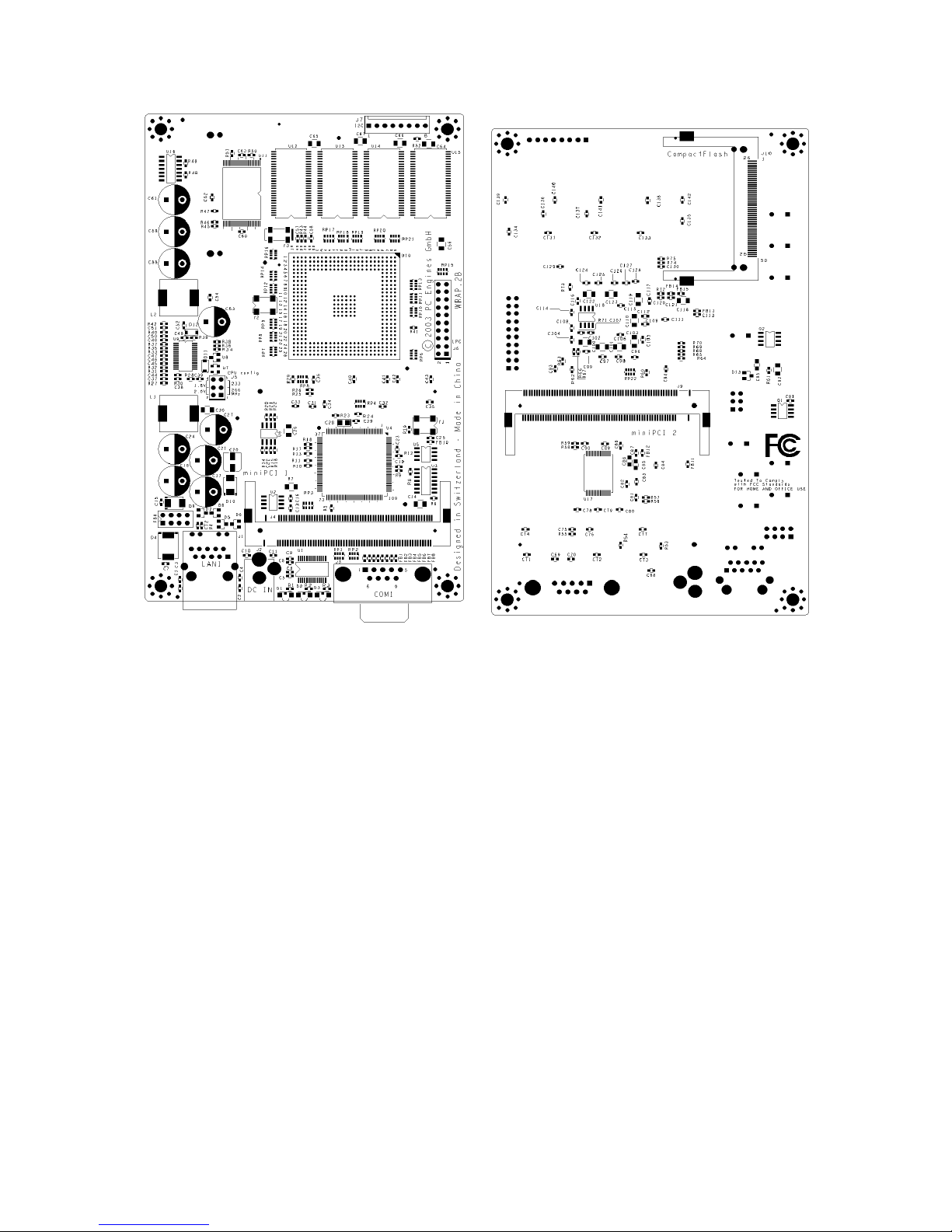
WRAP.2B connector pinouts
J1 Ethernet port 1
Same as WRAP.1C.
J2 DC power jack
Same as WRAP.1C.
J3 Console serial port
Same as WRAP.1C.
J4, J9 miniPCI sockets
Same as WRAP.1C.
J5 Clock & core voltage selection jumper
CPU speed and core voltage can be configured by shunt jumper. Recommended settings are 233
MHz / 1.8V and 266 MHz / 2.0V.
1-3 266 MHz 3-5 233 MHz CPU speed
2-4 2.0V 4-6 1.8V core voltage
J6 LPC expansion
Same as WRAP.1C.
J7 I2C / battery / watchdog header
This header can be used to connect user specific hardware, e.g. a front panel microcontroller, or for
a licensing dongle.
1 +3.3V power supply
2 SCL1 I2C clock
3 SDA1 I2C data
4 GND ground
5 DOGFOOD interface pin for watchdog, connected to CPU GPIO G14.
6 OVERTMP# overtemperature signal from thermal sensor. If this is pulled low, the CPU
will be reset.
7 VBAT RTC battery voltage, connect to +3V Lithium battery
8 GND ground
J10 CompactFlash
Same as WRAP.1C. WRAP.2B has optional support for on-board NAND flash. Please contact PC
Engines for details.

WRAP router platform 25 2/13/2007
WRAP.2B mechanical dimensions
All dimensions in units of 0.001” (0.0254 mm).

WRAP router platform 26 2/13/2007
POST codes
tinyBIOS writes POST / diagnostic codes to port 80h. To make these codes visible, use a miniPCI
POST card such as PC Engines POST.5A. POST codes are:
01 reset entry
02 chipset initialization
03 detect base memory size
04 initialize shadow RAM
05 init mono video
06 disable PCI devices
07 test low 64KB of DRAM
08 initialize stack
09 BIOS checksum
0a super I/O initialization
0b RTC test
0c refresh / 8254 test
0d speed-dependent chipset regs
0e test 8237 DMA
0f test DMA page registers
10 test 8254 registers
11 test keyboard controller
12 init timer, DMA, 8259...
13 test 8259 mask registers
14 test low 640KB
15 init vectors
16 PCI plug & play
17 shadow video BIOS
18 look for VGA BIOS
19 sign-on prompt
1a second keyboard test
1b extended memory test
1c enable interrupts
1d test / init RTC
1e init floppy disk
1f option ROM scan
20 test parallel ports
21 test serial ports
22 enable coprocessor
23 floppy init
24 hard disk init
25 PS/2 mouse detect
26 timer/RTC check
27 OEM boot decision point
00 boot
33 NMI
F7 low 64KB memory test failed

WRAP router platform 27 2/13/2007
Resources
Tools
POST cards, CompactFlash adapters, CompactFlash cards and other accessories are accessible from
PC Engines. Visit www.pcengines.ch for information.
tinyBIOS
The tinyBIOS manual can be found at www.pcengines.ch/tinybios.htm
Please note that the BIOS core used on this board has a few extra features. Full BIOS source code
can be licensed from PC Engines.
Literature
Please see www.pcengines.ch/resource.htm for pointers to literature and standards.
 Loading...