

Page 1

USER
MANUAL
MODEL 2701/B, C, D
G.703/G.704 NTU with
EIA-530, V.35, X.21
Interfaces
Important
intended for use in a light industrial environment. It is not intended nor approved for use
in an industrial or residential environment.
An ISO-9001CertiÞed
Company
—This is a Class A device and is
Part# 07M2701-UM
Doc# 08610U2-001
Rev. F
Revised 1/23/08
SALES OFFICE
(301) 975-1000
TECHNICAL SUPPORT
(301) 975-1007
Page 2

CONTENTS
1.0 Warranty & Compliance Information ........................................ 4
1.1 Compliance................................................................................... 4
EMC Compliance.......................................................................... 4
Safety Compliance: ...................................................................... 4
PSTN Regulatory Compliance:..................................................... 4
1.2 CE Notice...................................................................................... 5
1.3 Authorized European Representative........................................... 5
1.4 Service.......................................................................................... 5
1.5 Safety When Working With Electricity .......................................... 6
2.0 General Information.................................................................... 7
2.1 Features........................................................................................ 7
2.2 Description.................................................................................... 7
3.0 Configuration .............................................................................. 8
3.1 DIP Switch Configuration.............................................................. 8
Switch SW1-1 through SW1-5...................................................... 9
SW1-6 and SW1-7 Clock Modes................................................ 10
SW1-8: Enable/Disable Loop Tests from DTE ........................... 11
Switch SW2-1 Line Coding: HDB3 (default)............................... 11
Switch SW2-2: CRC-4 Multiframe .............................................. 12
Switch SW2-3 Data Inversion..................................................... 12
Switch SW2-4: Remote Digital Loopback Type.......................... 13
Switch SW2-5 Front Panel Switches.......................................... 13
Switch SW2-6: V.54 Response Disabled (default) ..................... 13
4.0 Installation................................................................................. 14
4.1 Connecting to the G.703 Network............................................... 14
Connecting the 2701/D (X.21 version) Dual Coaxial Cable
(75 ohm) to the G.703 Network .................................................. 14
Opening the Case....................................................................... 14
Connecting the Twisted Pair (120 ohm) to the G.703 Network .. 15
4.2 Connecting the Serial Port.......................................................... 15
Connecting to a “DTE” Device.................................................... 15
Connecting to a “DCE” Device ................................................... 16
Configuring the X.21 Interface (2701/D)..................................... 16
4.3 Power Connection ...................................................................... 16
Universal AC Power (100–240 VAC).......................................... 16
DC Power ................................................................................... 17
5.0 Operation................................................................................... 18
5.1 Power-up .................................................................................... 18
5.2 LED Status Monitors................................................................... 18
5.3 Loop (V.54 & Telco) Diagnostics ................................................ 19
Operating Local Loopback (LL) .................................................. 19
Operating Remote Digital Loopback (RL)................................... 20
CSU Loop................................................................................... 21
Using the V.52 (BER) Test Pattern Generator ........................... 22
2
Page 3

A
Specifications ........................................................................... 23
A.1 Network Data Rate ...................................................................... 23
A.2 Network Connector ..................................................................... 23
A.3 Nominal Impedance ................................................................... 23
A.4 Line Coding ................................................................................ 23
A.5 Line Framing ............................................................................... 23
A.6 CRC-4 Multiframing .................................................................... 23
A.7 Clocking ...................................................................................... 23
A.8 Time Slot Rate ............................................................................. 23
A.9 Network Data Rates .................................................................... 23
A.10 Distance ...................................................................................... 23
A.11 Configuration .............................................................................. 23
A.12 Power Supply .............................................................................. 24
A.13 Humidity ...................................................................................... 24
A.14 Temperature ............................................................................... 24
A.15 Dimensions ................................................................................. 24
B
Interface Pin Assignment......................................................... 25
C
Interface Pin Assignment......................................................... 27
D
Interface Pin Assignment......................................................... 29
E
Factory Replacement Parts and Accessories........................ 30
3
Page 4

1.0 WARRANTY & COMPLIANCE INFORMATION
Patton Electronics warrants all Model 2701/I components to be free from
defects, and will—at our option—repair or replace the product should it
fail within one year from the Þrst date of shipment.
This warranty is limited to defects in workmanship or materials, and does
not cover customer damage, abuse, or unauthorized modiÞcation. If this
product fails or does not perform as warranted, your sole recourse shall
be repair or replacement as described above. Under no condition shall
Patton Electronics be liable for any damages incurred by the use of this
product. These damages include, but are not limited to, the following: lost
proÞts, lost savings and incidental or consequential damages arising
from the use of or inability to use this product. Patton Electronics speciÞcally disclaims all other warranties, expressed or implied, and the installation or use of this product shall be deemed an acceptance of these
terms by the user.
1.1 COMPLIANCE
EMC Compliance
• EN55022, Class A
• EN55024
Safety Compliance:
• EN 60950-1
• AS/NZS 60950-1
PSTN Regulatory Compliance:
• TBR 12 & 13
• AS/ACIF S016:2001
4
Page 5

1.2 CE NOTICE
We certify that the apparatus identiÞed in this document conforms to the
requirements of Council Directive 1999/5/EC on the approximation of the
laws of the member states relating to Radio and Telecommunication Terminal Equipment and the mutual recognition of their conformity.
The safety advice in the documentation accompanying this product shall
be obeyed. The conformity to the above directive is indicated by the CE
sign on the device.
1.3 AUTHORIZED EUROPEAN REPRESENTATIVE
D R M Green
European Compliance Services Limited.
Oakdene House, Oak Road
WatchÞeld, Swindon, Wilts SN6 8TD, UK
1.4 SERVICE
All warranty and non-warranty repairs must be returned freight prepaid
and insured to Patton Electronics. All returns must have a Return Materials Authorization number on the outside of the shipping container. This
number may be obtained from Patton Electronics Technical Services at:
• Tel: +1
• Email:
• URL:
(301) 975-1007
support@patton.com
http://www.patton.com
Note
Packages received without an RMA number will not be
accepted.
5
Page 6
1.5 SAFETY WHEN WORKING WITH ELECTRICITY
• This device contains no user serviceable parts. The
equipment shall be returned to Patton Electronics for
repairs, or repaired by qualified service personnel.
• The external power adapter shall be a listed Limited
Power Source. Ensure that the power cable used meets
all applicable standards for the country in which it is to
be installed, and that it is connected to a wall outlet
which has earth ground. The mains outlet that is utilized to power the devise shall be within 10 feet (3
meters) of the device, shall be easily accessible, and
protected by a circuit breaker.
WARNING
• Hazardous network voltages are present in WAN ports
regardless of whether power to the unit is ON or OFF. To
avoid electric shock, use caution when near WAN ports.
When detaching the cables, detach the end away from
the device first.
• Do not work on the system or connect or disconnect
cables during periods of lightning activity.
In accordance with the requirements of council directive 2002/96/EC on Waste of Electrical and Electronic
Equipment (WEEE), ensure that at end-of-life you separate this product from other waste and scrap and deliver
to the WEEE collection system in your country for recycling.
6
Page 7

2.0 GENERAL INFORMATION
Thank you for your purchase of this Patton Electronics product. This
product has been thoroughly inspected and tested and is warranted for
One Year parts and labor. If any questions or problems arise during
installation or use of this product, please do not hesitate to contact Patton Electronics Technical Support at (301) 975-1007.
2.1 FEATURES
• Terminates G.703 and G.704, E1/fractional E1 service
• Available in low-cost standalone or rack-mountable versions
• n x 64 kbps data rates to 2 Mbps
• X.21, V.35, and EIA-530
• Switch-selectable AMI or HDB3 line encoding options
• Switch-selectable DTE/DCE modes for X.21 version
• 75-ohm dual coax and 120-ohm twisted-pair G.703 connections
• Local and remote loopback diagnostics
• Internal, external, and G.703 network timing
• CE approval
• 100–240 VAC and 48 VDC power options
• Conforms to ONP requirements CTR 12 and CTR 13 for connection to
international Telecom networks
2.2 DESCRIPTION
The Model 2701 receives channelized G.704 (n x 64 kbps) or clear channel E1/G.703 (2.048-Mbps) data from the Telco’s digital data network.
The Model 2701 terminates the G.703 telco interface and converts the
data for transmission to a user-oriented serial [X.21, V.35, and EIA-530
(V.36/RS422)]. The 2701 can connect to a Router, FRAD, PABX or Multiplexer over its serial interface at nx64kbps data rates up to 2.048 Mbps.
Thank you for your purchase of this Patton Electronics product. This
product has been thoroughly inspected and tested and is warranted for
One Year parts and labor. If any questions or problems arise during
installation or use of this product, contact Patton Electronics Technical
Support at (301) 975-1007.
7
Page 8
3.0 CONFIGURATION
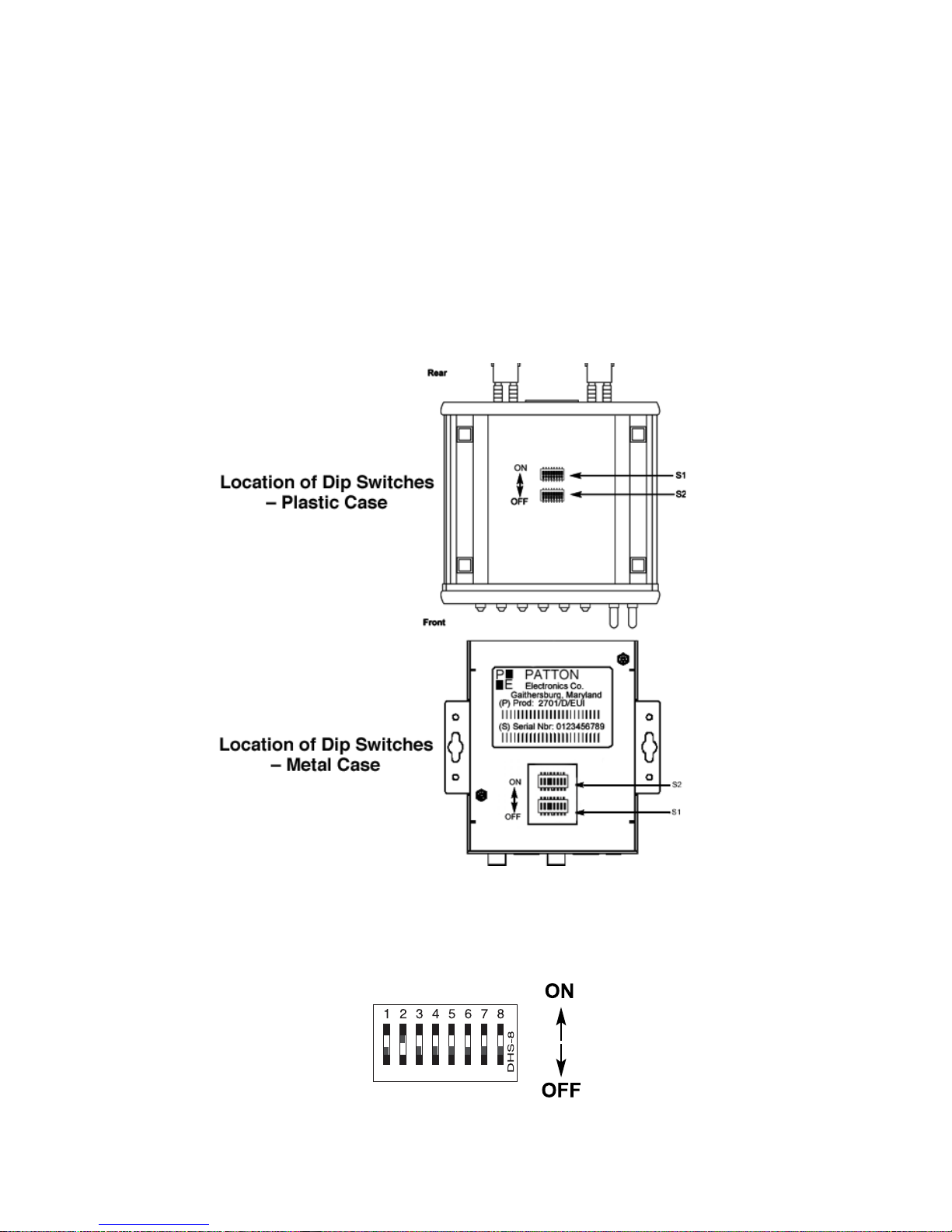
The Model 2701 features conÞguration capability via hardware DIP
switches. This section describes all possible DIP switch conÞgurations of
the Model 2701.
3.1 DIP SWITCH CONFIGURATION
The Model 2701 has two sets of internal DIP switches that allow conÞgu-
ration for a wide range of applications. The sets of switches are accessed
from the underside of the 2701. Figure 1 shows the location of the DIP
switches on the bottom of the printed circuit board.
Figure 1.
Underside of Model 2701, Showing Location of DIP Switches
The Model 2701 DIP switches (Switch Sets 1–2) can be conÞgured as
either “ON” or “OFF”. Figure 2 shows the orientation of the DIP switches
with respect to ON/OFF positions.
Figure 2.
Close up of conÞguration switches
8
Page 9

Switch SW1-1 through SW1-5
A detailed description of each switch (SW1-1 through SW1-5) setting follows the summary table below.
SW1
On
Table 1:
SW2 SW3 SW4 SW5 Speed
On On On On 64 kbps
Switch Set 1 Summary Table
Off On On On On 128 kbps
On Off On On On 192 kbps
Off Off On On On 256 kbps
On On Off On On 320 kbps
Off On Off On On 384 kbps
On Off Off On On 448 kbps
Off Off Off On On 512 kbps
On On On Off On 576 kbps
Off On On Off On 640 kbps
On Off On Off On 704 kbps
Off Off On Off On 768 kbps
On On Off Off On 832 kbps
Off On Off Off On 896 kbps
On Off Off Off On 960 kbps
Off Off Off Off On 1024 kbps
On On On On Off 1088 kbps
Off On On On Off 1152 kbps
On Off On On Off 1216 kbps
Off Off On On Off 1280 kbps
9
Page 10

SW1 SW2 SW3 SW4 SW5 Speed
On On Off On Off 1344 kbps
Off On Off On Off 1408 kbps
On Off Off On Off 1472 kbps
Off Off Off On Off 1536 kbps
On On On Off Off 1600 kbps
Off On On Off Off 1664 kbps
On Off On Off Off 1728 kbps
Off Off On Off Off 1792 kbps
On On Off Off Off 1856 kbps
Off On Off Off Off 1920 kbps
On Off Off Off Off 1984 kbps
Off Off Off Off Off Clear Channel 2048 kbps
Note
When the data rate is set to 2.048Mb/s, the unit is forced into
G.703 mode, and it transmits user data on all 32 time-lots. There
is no framing information; therefore, the CRC4 MF (SW2-2)
switch is ignored. In all other rate settings, the unit employs
G.704 framing; TS0 is reserved for signaling.
SW1-6 SW1-7 Clock Mode
On On Network (Received Recovered)
On Off Internal
Off On External
Off Off Network (Received Recovered)
SW1-6 and SW1-7 Clock Modes
Use Switches SW1-6 and SW1-7 to conÞgure the 2701 for internal,
external, or receive recover clock mode.
Network Clock
—Transmitter timing is derived using the received line
signal (received recovered) from the network.
Internal Clock
—Transmitter timing is derived from an internal clock
source.
External Clock
—Transmitter timing is derived from DTE terminal timing.
10
Page 11

SW1-8: Enable/Disable Loop Tests from DTE
Use Switch SW1-8 to allow Model 2701 to enter loopback tests when the
DTE raises the appropriate loop request pin.
S1-8
Off
Response to DTE Loopback Request Enabled
Setting
On Response to DTE Loopback Request Disabled
Position Function Factory Default Selected Option
SW2-1 Line Coding Off HDB3
SW2-2 CRC-4 multiframe Off Disabled
SW2-3 Data Inversion Off Data Not Inverted
SW2-4 V.54/CSU select Off V.54 RDL loop
SW2-5 FPS enabled Off Enabled
SW2-6 V.54 Response On Disabled
SW2-7 Not Used N/A N/A
SW2-8 Not Used N/A N/A
Switch SW2-1 Line Coding: HDB3 (default)
Use Switch SW2-1 to control the Network Line Coding options. Set these
options to be the same as the Line Coding given to you by your Service
Provider. If you are using two Model 2701s together as short range
modems, set both units to HDB3.
Options:
HDB3
AMI
SW2-1
Off
Line Encoding
HDB3
On AMI
HDB3, AMI
In this line coding, the transmitter substitutes a deliberate bipolar violation when excessive zeros in the data stream are
detected. The receiver recognizes these special violations and
decodes them as zeros. This method enables the network to
meet minimum pulse density requirements. Unless AMI is
required in your application, HDB3 should be used whenever
possible.
Alternate Mark Inversion deÞnes a pulse as a “mark,” a binary
one, as opposed to a zero. In an E1 network connection, signals
are transmitted as a sequence of ones and zeros. Ones are
sent as pulses, and zeros are sent as spaces, i.e., no pulse.
11
Page 12

Every other pulse is inverted from the previous pulse in polarity,
so that the signal can be effectively transmitted. This means,
however, that a long sequence of zeros in the data stream will
cause problems, since the NTU receiving the signal relies on
the signal to recover the 2.048 Mb/s clock.
If you must use AMI, you should ensure that the data terminal
equipment connected to the unit provides a minimally acceptable pulse density. For this reason, there are advantages to
using HDB3 instead. AMI coding does not inherently account for
ones density. To meet this requirement, the user should ensure
that the data inherently meets pulse density requirements.
Switch SW2-2: CRC-4 Multiframe
In framed mode, SW2-2 is used for CRC-4 MF. When CRC-4 is enabled,
the unit monitors the incoming data stream for CRC-4 errors. It transmits
CRC-4 error counts to the transmitting unit. When using timeslot zero
(TS0), excessive errors may cause loss of frame or loss of sync. If CRC4 MF is used, both units must be set for set for CRC-4 MF. Otherwise, the
one using CRC-4 MF will detect loss of sync.
SW2-2
Off
Option
CRC-4 Disabled
On CRC-4 Enabled
Note
When the data rate is set to 2.048Mb/s, then the unit is forced
into G.703 mode, and it transmits user data on all 32 time-lots.
There is no framing information; therefore, the CRC4 MF (SW2-
2) switch is ignored. In all other rate settings, the unit employs
G.704 framing; TS0 is reserved for signaling.
Switch SW2-3 Data Inversion
Set Switch S2-3 to determine whether or not the data stream from the
local DTE is inverted within the Model 2701 before being passed to the
G.703/G.704 network. An inverted data stream may be required when
you use the Model 2701 to communicate with a G.703 device (that
inverts the data) on the remote end. In typical installations, data inversion
is not necessary.
SW2-3 Option
Off
Data not inverted
On Data inverted
12
Page 13

Switch SW2-4: Remote Digital Loopback Type
The user can set this switch to select the type of remote loop that will be
initiated by the Model 2701. If set to V.54, the Model 2701 will initiate a
V.54 loop when Remote Loop is selected by the front panel switches. If
set to CSU, the Model 2701 will initiate a CSU loop when Remote Loop
is selected by the front panel switches.
S2-4
Off
Initiate a V.54 RDL loop when selected
RDL Type
On Initiate a CSU loopback when selected
Switch SW2-5 Front Panel Switches
As the Front Panel Switches may be inadvertently toggled, or in the
event that the end-user may not need to use the switches, the installer
may disable the front panel switches. Set Switch S2-5 to determine
whether the front-panel toggle switches are active or inactive.
SW2-5
Off
Front Panel Switches Enabled
Option
On Front Panel Switches Disabled
Switch SW2-6: V.54 Response Disabled (default)
V.54 Response is a special in-band loopback facility that sends a
pseudo-random pattern over the data stream. This is the only loopback
that the unit can initiate. This is useful for campus applications when you
need to put a remote unit in loopback. The unit responds to the V.54 loopback command, and the whole process takes only a few seconds to complete. When V.54 Loopback is disabled, the unit will not be able to send
or respond to V.54 loopback commands. The duration of the loopback is
limited by the loopback timeout setting.
SW2-6 Option
Off
V.54 Response Enabled
On V.54 Response Disabled
13
Page 14

4.0 INSTALLATION
The Interconnecting cables shall be acceptable for
external use and shall be rated for the proper application with respect to voltage, current, anticipated tem-
CAUTION
perature, flammability, and mechanical serviceability.
Once the Model 2701 is properly conÞgured, it is ready to connect to the
G.703/G.704 interface, to the serial port, and to the power source. This
section describes how to make these connections.
4.1 CONNECTING TO THE G.703 NETWORK
The Power, G.703/G.704 and serial Line connections are located on the
rear panel of the Model 2701. The following sections describe operation
of these connections.
Connecting the 2701/D (X.21 version) Dual Coaxial Cable
(75 ohm) to the G.703 Network
The Model 2701/D (X.21 version) is equipped with dual female BNCs
(TX and RX) for connection to a 75 ohm dual coax G.703 network interface. If your G.703/G.704 network terminates via dual coaxial cable, use
the diagram below to make the proper connections. See Figure 3.
Note
Figure 3.
The outer conductor of the coax cables are isolated from system
earth ground.
Rear Panel, Showing Location of Connectors.
When using the 75 Ohm interface, jumper straps JP2, JP5, JP6, and JP7
must be installed over the jumpers. The jumpers are located next to the
BNC connectors. Refer to the following section to open the case. Open
the case and install jumper straps for JP2, JP5, JP6, and JP7.
Opening the Case
Open the case by inserting a screwdriver into the slots and twist the
screwdriver head slightly. The top half of the case will separate from the
14
Page 15

lower half of the case. Take caution not to damage any of the PC board
SIG
SIG
mounted components.
Connecting the Twisted Pair (120 ohm) to the G.703 Network
The Model 2701 is equipped with a single RJ-48C jack for connections to
a 120 ohm twisted pair G.703/G.704 network interface. If your G.703/
G.704 network terminates via RJ-48C, use the connection diagram
(Figure 4) following the pinout and signals chart below to connect the
120 ohm G.703/G.704 network channel.
NETWORK
NAL
NAL
PIN#
RX(R) 1-----------------------TX(R)
RX(T) 2-----------------------TX(T)
TX(R) 4-----------------------RX(R)
TX(T) 5-----------------------RX(T)
Shield 3-----------------------Shield
Shield 6-----------------------Shield
Signal NameRJ-48C Jack
1
(RX) Receive (Ring)
1
2
3
4
5
6
7
8
2
(RX) Receive (Tip)
3
Shield
4
(TX) Transmit (Ring)
5
(TX) Transmit (Tip)
6
Shield
7
No connection
8
No connection
4.2 CONNECTING THE SERIAL PORT
The Model 2701/B, C, D supports RS-530, V.35, X.21 serial port connections. This section describes how to connect the serial ports to your terminal equipment.
Connecting to a “DTE” Device
The serial port on the 2701/B (RS-530 version) and 2701/C (V.35 version) is hard-wired as a DCE. Therefore these modules “want” to plug
Figure 4.
G.703/G.704 170 ohm Connection.
15
Page 16

into a DTE such as a terminal, PC or host. When making the connection
to your DTE device, use a straight through cable of the shortest possible
length—we recommend 6 feet or less. When purchasing or constructing
an interface cable, please refer to the pin diagrams in Appendix D as a
guide.
Connecting to a “DCE” Device
If the Model 2701 serial interface is hard-wired as a DCE (all except the
X.21 version), you must use a null modem cable when connecting to a
modem, multiplexer or other DCE device. This cable should be of the
shortest possible length—we recommend 6 feet or less.
ConÞguring the X.21 Interface (2701/D)
The serial port on the X.21 interface is default wired as a DCE, but may
be switched to a DTE. This is done by reversing the orientation of the
DCE/DTE strap, as described below:
To reverse DCE/DTE orientation, remove the top case. Refer to section
“Opening the Case” on page 14
The DCE/DTE strap is located near the DB15 connector on the top side
of the board. The arrows on the top of the strap indicate the conÞguration
of the X.21 port (for example, if the DCE arrows are pointing toward the
DB-15 connector, the X.21 port is wired as a DCE). Reverse the DCE/
DTE orientation by pulling the strap out of its socket, rotating it 180º, then
plugging the strap back into the socket. You will see that the DCE/DTE
arrows now point in the opposite directions, showing the new conÞguration of the X.21 port.
Note
If the 2701/D is conÞgured as a DTE, the clocking mode must be
set for external clock.
4.3 POWER CONNECTION
Universal AC Power (100–240 VAC)
The Model 2701 uses a 5VDC, 2A universal input 100–240 VAC, power
supply (center pin is +5V). The universal input power supply has a male
IEC-320 power entry connector. This power supply connects to the
Model 2701 by means of a barrel jack on the rear panel. Many international power cords are available for the universal power supply.
The Model 2701 powers up as soon as it is plugged into an AC outlet-there is no power switch.
16
Page 17

DC Power
The 36-60 VDC DC to DC adapter is supplied with the DC version of the
Model 2701. The black and red leads plug into a DC source (nominal
48VDC) and the barrel power connector plugs into the barrel power supply jack on the 2701. (See Figure 5).
To Power
Supply Jack
Barrel power connector
Figure 5.
WARNING
SWITCHING POWER SUPPLY
MODEL : SYD1106-0505
INPUT : 36-60V 0.2A MAX
OUTPUT : +5V 1.0A
S/N: G01234567890
MADE IN CHINA BY SUNNY
OUTPUT POWER : 5W MAX
-Vin
+Vin
To -48VDC
Source
Black lead (-V)
Red lead (+V)
Connecting DC Power to the 2701 DC Power Supply.
There are no user-serviceable parts in the
power supply section of the Model 2701. Contact Patton Electronics Technical support at
(301)975-1007, via our web site at http://
www.patton.com, or by e-mail at support@patton.com, for more information.
17
Page 18

5.0 OPERATION
When the Model 2701 has been properly conÞgured and installed, it
should operate transparently. This sections describes power-up, LED
status monitors, and the built-in loopback test modes.
5.1 POWER-UP
Before applying power to the Model 2701, please read “Power Connection” on page 16 and verify that the unit is properly connected to the
appropriate power source.
5.2 LED STATUS MONITORS
The Model 2701 features six front panel LEDs that monitor connections
on the G.703/G.704 and signaling, error and test modes. Figure 6 shows
the front panel location of each LED. Descriptions of each LED follow
Figure 6.
E1 Link
(Active Green) Solid green (On) indicates that the end to end E1
Link is up, signifying that the link is active. The E1 Link LED is
Off when the link is down.
Figure 6.
2701 Front Panels
18
Page 19

TD & RD
LOS
ER
TM
Glows yellow to indicate an idle condition of Binary “1” data on
the respective terminal interface signals. Green indicates Binary
“0” data.
The Loss of Sync LED lights when the unit loses synchronization with the incoming signal. This may happen when there is a
framing mismatch or a loss of signal. In unframed mode, the
LOS LED monitors the status of the transmit clock.
The error LED indicates various error conditions, including framing bit errors, excessive zeros, controlled slips, severe errors, or
bit errors (when sending V.52 test patterns). When sending a
test pattern, the LED will remain lit if the unit does not receive
the identical pattern. When it receives the correct pattern, the
LED will turn off. If error insertion is on, the LED will blink once a
second if everything is operating properly.
(Active Yellow) Solid Yellow indicates an Active Test Mode. The
unit may be placed in test mode by the local user or by the
remote user.
5.3 LOOP (V.54 & TELCO) DIAGNOSTICS
The Model 2701 offers three V.54 loop diagnostics. Use these diagnostics to test the NTU and any communication links. These tests can be
activated via the front panel switches or via signals on the Model 2701/B
and C serial port interface.
Operating Local Loopback (LL)
The Local Loopback (LL) test checks the operation of the local Model
2701, and is performed separately on each unit. Any data sent to the
local Model 2701 in this test mode will be echoed (returned) back to the
user device (i.e., characters typed on the keyboard of a terminal will
appear on the terminal screen).
19
Page 20

Figure 7.
Local Loopback for a Network Termination Application
To perform a LL test, follow these steps:
1. Activate LL. This may be done in one of two ways:
— Place the switch on the front panel in the “Local” position.
— Activate the “LL” signal on the DTE (2701/B and 2701/C only).
If you are not sure which lead is the “LL” signal, please refer to
Appendix D.
2. Verify that the data terminal equipment is operating properly and
can be used for a test.
3. Perform a V.52 BER (bit error rate) test as described in section
“Using the V.52 (BER) Test Pattern Generator” on page 22. If the
BER test equipment indicates no faults, but the data terminal indicates a fault, follow the manufacturer’s checkout procedures for the
data terminal. Also, check the interface cable between the terminal
and the Model 2701.
Operating Remote Digital Loopback (RL)
The Remote Digital Loopback (RL) test checks the performance of both
the local and remote NetLink-E1™, as well as the communication link
between them. Any characters sent to the remote NetLink-E1™ in this
test mode will be returned back to the originating device (i.e, characters
typed on the keyboard of the local terminal will appear on the local terminal screen after having been passed to the remote NetLink-E1™ and
looped back).
20
Page 21

Figure 8.
Remote Loop in a Network Extension Application
There are two Remote Loops that can be initiated from the NetLink-E1
unit: (1) V.54 Loop, and; (2) CSU Loop. The user can select the type of
loop that can be initiated by Switch S2-4. When a loopback is initiated
this is the type of loop that the unit uses to loop up the remote unit and
which type of loop the unit will respond to.
To perform an RDL test, follow these steps:
1. Activate RDL. This may be done in two ways:
— Activate the “RL” signal on the DTE (2701/B and 2701/C only). If
you are not sure which lead is the “RL” signal, please refer to
Appendix B or C, depending on the version you are using.
— Set the front panel switch to “Remote”.
2. Perform a bit error rate test (BERT) using the internal V.52 generator (as described in section “Using the V.52 (BER) Test Pattern
Generator”), or using a separate BER Tester. If the BER test indicates a fault, and the Local Line Loopback test was successful for
both NetLink devices, you may have a problem with the twisted
pair line connection.
CSU Loop
Although CSU Loop is predominantly a T1 function, the NetLink-2701
responds to central ofÞce initiated loop commands. Customers can use
this facility when the Central OfÞce network switch supports CSU loops
over an E1 interface.
When CSU Loop is selected, the NetLink 2701 will implement the “loop
up” command when it recognizes the pattern “10000” in the data stream
for a minimum of 5 seconds. The “loop down” command is implemented
by the pattern “100” in the data stream for a minimum of 5 seconds.
21
Page 22

The NetLink 2701 will respond to Universal Loopback De-activate to
clear all central ofÞce loops.
Using the V.52 (BER) Test Pattern Generator
To use the V.52 BER tests in conjunction with the Remote Digital Loopback tests (or with Local Line Loopback tests), follow these instructions:
1. Locate the “511/511E” toggle switch on the front panel of the 2701
and move it UP. This activates the V.52 BER test mode and transmits
a “511” test pattern into the loop. If any errors are present, the local
modem’s red “ER” LED will illuminate.
2. If the above test indicates no errors are present, move the V.52 toggle switch DOWN, activating the “511/E” test with errors present. If
the test is working properly, the local modem's red “ER” LED will
blink once every second. A successful “511/E” test will conÞrm that
the link is in place, and that the Model 2701’s built-in “511” generator
and detector are working properly.
Note
The above V.52 BER tests can be used independently of the
Remote Digital Loopback tests. This requires two operators: one
to initiate and monitor the tests at the local Model 2701, and one
to do the same at the remote Model 2701. In this case, the test
pattern sent by each Model 2701 will not be looped back, but will
be transmitted down the line to the other Model 2701. While one
operator initiates test, the other monitors for errors.
22
Page 23

APPENDIX A
SPECIFICATIONS
A.1 NETWORK DATA RATE
2.048 Mbps
A.2 NETWORK CONNECTOR
RJ-48C/Dual Coax BNC (2701/D)
A.3 NOMINAL IMPEDANCE
75/120 ohm
A.4 LINE CODING
Selectable AMI or HDB3
A.5 LINE FRAMING
G.703 (Unframed) or G.704/G.732 (Framed)
A.6 CRC-4 MULTIFRAMING
Selectable On or Off
A.7 CLOCKING
Internal, External, or Network (Receive Recover)
A.8 TIME SLOT RATE
64 kbps
A.9 NETWORK DATA RATES
64, 128, 192, 256, 320,384, 448, 512, 576, 640, 704, 768, 832, 896, 960,
1024, 1088, 1152, 1216, 1280, 1344, 1408, 1472, 1536, 1600, 1664,
1728, 1792, 1856, 1920, 1984, 2048 kbps
A.10 DISTANCE
Maximum 1.6 km (5,250 ft.) on 24 AWG Cable
A.11 CONFIGURATION
Two 8-Position DIP Switches
23
Page 24

A.12 POWER SUPPLY
+5 VDC External power supply/100–240 VAC, 50–60Hz, 0.4A
A.13 HUMIDITY
Up to 90% non-condensing
A.14 TEMPERATURE
0 to 50°C (32 to 122°F)
A.15 DIMENSIONS
Plastic Case – 9.0L x 5.3W x 2.0H cm (3.5L x 2.1W x 0.78H in.)
Metal Case – 3.2L x 13.8W x 14.6H cm (1.25L x 5.43W x 5.75H in)
24
Page 25

APPENDIX B
INTERFACE PIN ASSIGNMENT
EIA-530 Interface Pin Description
(DB-25 Female Connector)
(DCE ConÞguration)
Pin # Signal
1 FG (Frame Ground)
2 TD (Transmit Data)
3 RD (Receive Data)
4 RTS (Request to Send)
5 CTS (Clear to Send)
6 DSR (Data Set Ready)
7 SGND (Signal Ground)
8 CD (Carrier Detect)
9 RC/ (Receive Timing-B)
10 CD/ (Carrier Detect-B)
11 XTC/ (External Transmit Clock)
12 TC/ (Transmit Clock-B)
13 CTS/ (Clear to Send)
14 TD/ (Transmit Data-B)
15 TC (Transmit Clock-A)
16 RD (Receive Data)
17 RC (Receive Timing)
18 LLB (Local Line Loop)
19 RTS/ (Request to Send)
20 DTR (Data Terminal Ready)
21 DL (Remote Digital Loop)
22 DSR/ (Data Set Ready)
23 DTR/ (Data Terminal Ready)
24 XTC (External Transmit Clock)
25 TM (Test Mode)
25
Page 26

RS-530 TO RS-530
(STRAIGHT THROUGH
CABLE) PIN OUT
RS-530 TO RS-530 (CROSS OVER
CABLE) PIN OUT
Pin # Function Pin # Function Pin #
1 Shield (A) 1 Shield (A) 1
2 TD (A) 2 RD (A) 3
3 RD (A) 3 TD (A) 2
4 RTS (A) 4 RLSD (A) 8
5 NC 5 NC 5
6 NC 6 NC 6
7 Signal Ground 7 Signal Ground 7
8 RLSD (A) 8 RTS (A) 4
9 RX Timing DCE (B) 9 TX Timing DTE (B) 11
10 RLSD (B) 10 RTS (B) 19
11 TX Timing DTE (B) 11 RX Timing DCE (B) 17
12 NC 12 NC 12
13 NC 13 NC 13
14 TD (B) 14 RD (B) 16
15 NC 15 NC 15
16 RD (B) 16 TD (B) 14
17 RX Timing DCE (A) 17 TX Timing DTE (A) 11
18 NC 18 NC 18
19 RTS (B) 19 RLSD (B) 10
20 NC 20 NC 20
21 NC 21 NC 21
22 NC 22 NC 22
23 NC 23 NC 23
24 TX Timing DTE (A) 24 RX Timing DCE (A) 17
25 NC 25 NC 25
26
Page 27

APPENDIX C
INTERFACE PIN ASSIGNMENT
V.35 Interface
(M/34F Female Connector)
(DCE ConÞguration)
Pin # Signal
B SGND (Signal Ground)
C RTS (Request to Send)
D CTS (Clear to Send)
E DSR (Data Set Ready)
F CD (Carrier Detect)
H DTR (Data Terminal Ready)
L LLB (Local Line Loop)
M TM (Test Mode)
N RDL (Remote Digital Loop)
P TD (Transmit Data)
R RD (Receive Data)
S TD/ (Transmit Data-B)
T RD/ (Receive Data-B)
U XTC (External Transmit Clock)
V RC (Receive Timing)
W XTC/ (External Transmit Clock)
X RC/ (Receive Timing)
Y TC (Transmit Clock-A)
AA TC/ (Transmit Clock-B)
27
Page 28

V.35 TO V.35 (STRAIGHT
THROUGH CABLE) PIN
OUT
V.35 TO V.35 (CROSS OVER
CABLE) PIN OUT
Pin Function Pin Function Pin
A Frame Ground A Frame Ground A
B Signal Ground B Signal Ground B
C RTS C DCD F
D NC D NC D
E DSR E DTR H
F DCD F RTS C
H DTR H DSR E
K NC K NC K
L NC L NC L
P TD (A) P RD (A) R
R RD (A) R TD (A) P
S TD (B) S RD (B) T
T RD (B) T TD (B) S
U SCTE (A) U RT (A) V
V RT (A) V SCTE (A) U
W SCTE (B) W RT (B) X
X RT (B) X SCTE (B) W
Y NC Y NC Y
AA NC AA NC AA
28
Page 29

APPENDIX D
INTERFACE PIN ASSIGNMENT
X.21 Interface
(DB-15 Female Connector)
(DTE /DCE ConÞguration)
Pin # Signal
1 Frame Ground
2 T (Transmit Data-A)
3 C (Control-A)
4 R (Receive Data-A)
5 I (Indication-A)
6 S (Signal Element Timing-A)
7 BT (Byte Timing-A)
8 SGND (Signal Ground)
9 T/ (Transmit Data-B)
10 C/ (Control-B)
11 R/ (Receive Data-B)
12 I/ (Indication-B)
13 S/ (Signal Element Timing-B)
14 BT/ (Byte Timing-B)
29
Page 30

APPENDIX E
FACTORY REPLACEMENT PARTS AND ACCESSORIES
Patton Model # Description
2701/B G.703/G.704 NTU with RS-530 interface
2701/C G.703/G.704 NTU with a V.35 interface
2701/D G.703/G.704 NTU with an X.21 interface
2701/I G.703/G.704 NTU w/ 10Base-T EN interface
0805US American Power Cord
0805EUR European Power Cord CEE 7
0805UK United Kingdom Power Cord
0805AUS Australia/New Zealand Power Cord
0805DEN Denmark Power Cord
0805FR France/Belgium Power Cord
0805IN India Power Cord
0805IS Israel Power Cord
0805JAP Japan Power Cord
0805SW Switzerland Power Cord
08055DCUI Universal Input Power Supply
07M2701 User Manual
30
Page 31

NOTES
_______________________________________________________
_______________________________________________________
_______________________________________________________
_______________________________________________________
_______________________________________________________
_______________________________________________________
_______________________________________________________
_______________________________________________________
_______________________________________________________
_______________________________________________________
_______________________________________________________
_______________________________________________________
_______________________________________________________
_______________________________________________________
_______________________________________________________
_______________________________________________________
_______________________________________________________
_______________________________________________________
_______________________________________________________
_______________________________________________________
_______________________________________________________
_______________________________________________________
_______________________________________________________
_______________________________________________________
31
Page 32

NOTES
_______________________________________________________
_______________________________________________________
_______________________________________________________
_______________________________________________________
_______________________________________________________
_______________________________________________________
_______________________________________________________
_______________________________________________________
_______________________________________________________
_______________________________________________________
_______________________________________________________
_______________________________________________________
_______________________________________________________
_______________________________________________________
_______________________________________________________
_______________________________________________________
_______________________________________________________
_______________________________________________________
_______________________________________________________
_______________________________________________________
_______________________________________________________
Copyright © 2007
Patton Electronics Company
All Rights Reserved.
32
 Loading...