

Page 1
USER
MANUAL
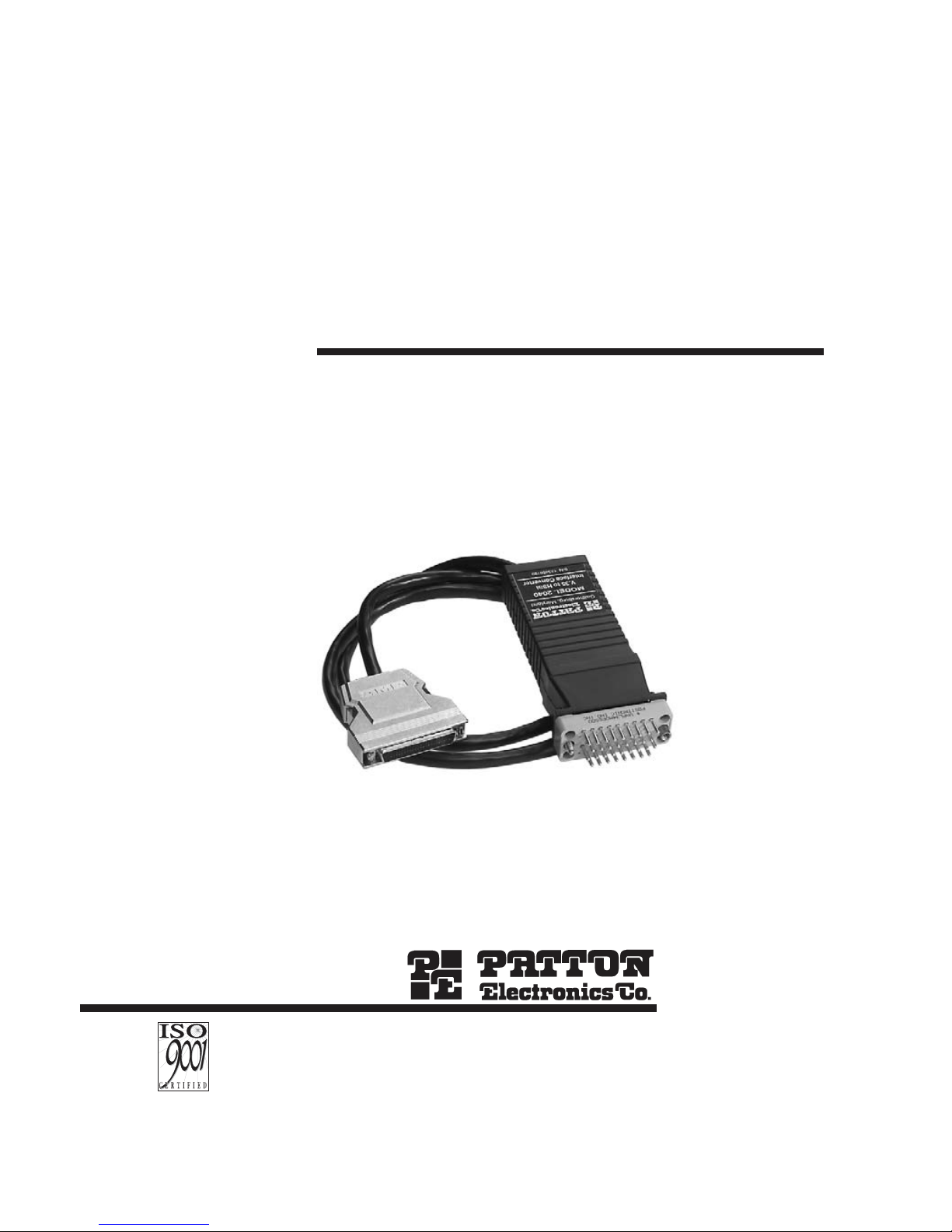
MODEL 2040 Series
V.35/RS-422 to HSSI
Interface Converter
SALES OFFICE
(301) 975-1000
TECHNICAL SUPPORT
(301) 975-1007
http://www.patton.com
Part# 07M2040-UM
Doc# 07720U2-001,
Rev. D
Revised 1/22/08
CERTIFIED
An ISO-9001
Certified Company
Page 2

Page 3

1.3 SERVICE
All warranty and nonwarranty repairs must be returned freight
prepaid and insured to Patton Electronics. All returns must have a
Return Materials Authorization number on the outside of the shipping
container. This number may be obtained from Patton Electronics
Technical Service at (301) 975-1007, http://www.patton.com, or at
support@patton.com.
NOTE: Packages received without an RMA number will not be
accepted.
Patton Electronics' technical staff is also available to answer any
questions that might arise concerning the installation or use of your
Model 2040. Technical Service hours: 8AM to 5PM EST, Monday
through Friday.
2
Page 4

Page 5
3.0 CONFIGURATION
The Model 2040 is easy to install and is ruggedly designed for
excellent reliability. The following instructions will help you set up and
install the Model 2040 properly.
To use the Patton Model 2040, you must first configure the unit for
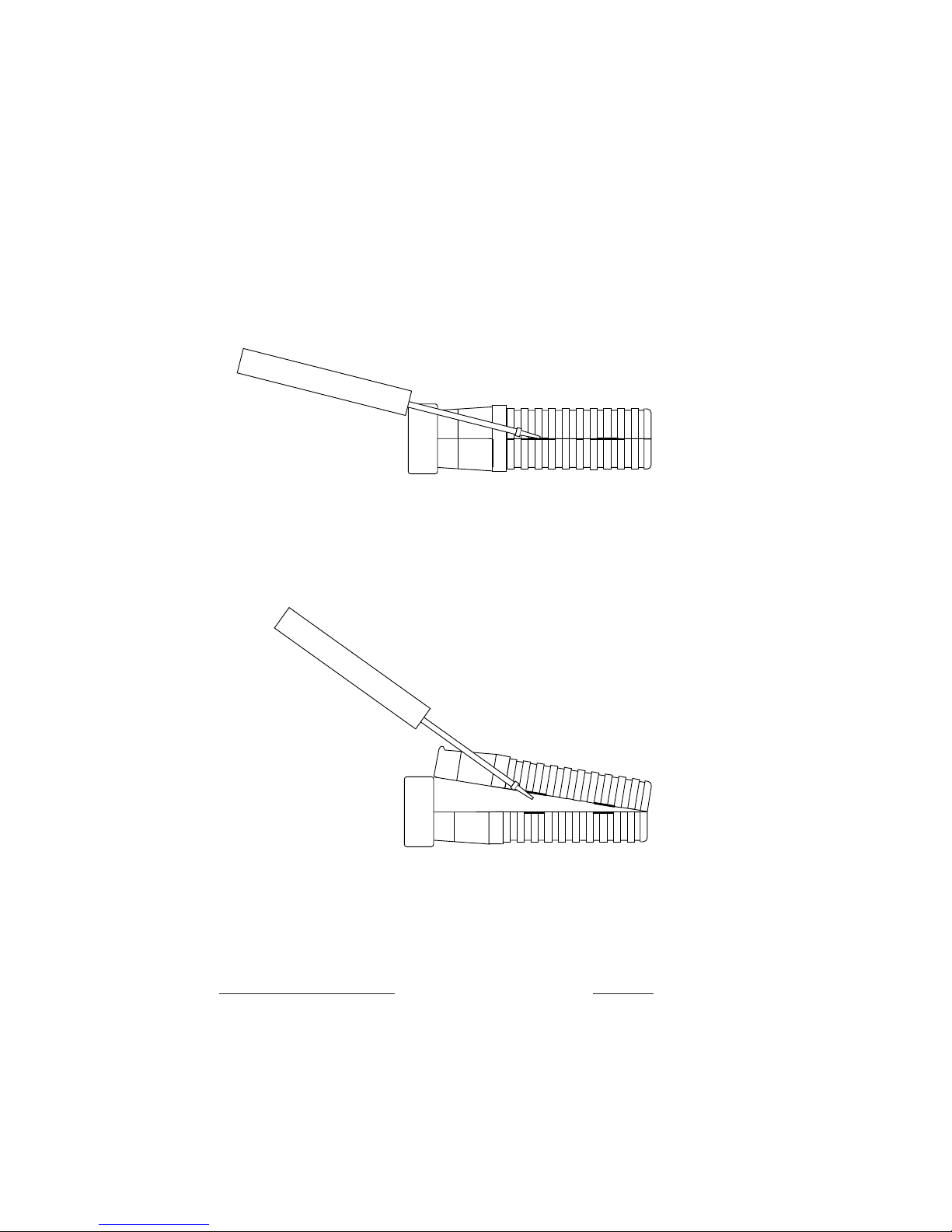
your application. To do so, first open the case by inserting a flat head
screw driver into an open slot on either side of the case, as in Figure 1.
Twist the screw driver head slightly and the top half of the case will
separate from the lower half, as in Figure 2. You now have access to
the internal switches used to configure the unit.
After opening the case, please refer to the section that pertains to
your unit for configuration details:
Patton Model Number
Section
Model 2040MC-MT and 2040MC-MT-422 ................3.1
Model 2040MT-MC and 2040MT-MC-422 ................3.2
To close the case, fit the 2 halves together snugly and snap them
back in place.
4
Figure 1: Using a Small Screw Driver to Open the Model 2040 Case
Figure 2: Using a Small Screw Driver to Open the Model 2040 Case
Page 6

Page 7
Switches S1-1 and S1-2: Clock Source
The setting for Switches S1-1 and S1-2 determines the source of
the HSSI Terminal Timing (TT). With Switch S1-1 On and S1-2 Off, the
Model 2040MC-MT derives the HSSI Terminal Timing from the ST
signal provided by the HSSI DCE. With Switch S1-1 Off, and S1-2 On,
the V.35 (or RS-422) DTE provides TT to the HSSI DCE.
S1-1
S1-2 Description
Off Off Not a Valid Setting
Off On Terminal Timing Supplied by V.35 (RS-422)
DTE device
On Off Terminal Timing supplied by HSSI ST signal
On On Not a Valid Setting
Switches S1-3 and S1-4: Synchronization Method
Switches S1-3 and S1-4 allow the Model 2040 to compensate for
timing delays when transmitting HSSI data at high speeds (greater than
2.5 Mbps). At high bit rates, set Switch S1-3 On and Switch S1-4 Off.
In this setting, the V.35 or RS-422 data will be synchronized to the SD
timing signal before conversion to HSSI. At lower bit rates (less than
2.5 Mbps), set Switch S1-3 Off and S1-4 On. In this setting, the V.35
(or RS-422) data bypasses the synchronization circuit and is passed
straight through to the HSSI DCE.
S1-3
S1-4 Description
Off Off Not a Valid Setting
Off On Data Skips Sync Circuit
On Off Data passes through sync circuit.
On On Not a Valid Setting
6
2040MC-MT DIP SWITCH SUMMARY TABLE
Position Function Factory Default
S1-1 Clock Source On
S1-2 Clock Source Off
S1-3 Sync Method Off
}
}
HSSI ST
Signal
Bypass
Sync Circuit
Tab le 1. DIP Switch S1 Default Settings for Model 2040MC-MT
Page 8

Page 9

Switches S1-1 and S1-2: Gapped Clock
Switches S1-1 and S1-2 allow the Model 2040MT-MC to generate
a HSSI gapped clock. Gapped clocking is a method of flow control in
which data flow is interrupted by an idle (gapped) clock signal. In this
mode, the Model 2040MT-MC will gap the ST clock to the HSSI DTE
whenever the V.35 (or RS-422) CTS signal is de-asserted. In the ‘No
Gapped Clock’ setting, the V.35 clock passes through with only a level
change.
S1-1
S1-2 Description
Off Off Not a Valid Setting
Off On Gapped Clock
On Off No Gapped Clock
On On Not a Valid Setting
Switches S1-3 and S1-4: Synchronization Method
Switches S1-3 and S1-4 allow the Model 2040MT-MC to
compensate for timing delays when transmitting HSSI data at high
speeds (greater than 2.5 Mbps). At high bit rates, set Switch S1-3 On
and Switch S1-4 Off. In this setting, the V.35 (or RS-422) data signals
will be synchronized to the SD timing signal before conversion to HSSI.
At lower bit rates (less than 2.5 Mbps), set Switch S1-3 Off and S1-4
On. In this setting, the V.35 (or RS-422) data bypasses the
synchronization circuit and is passed straight through to the HSSI DTE.
S1-3
S1-4 Description
Off Off Not a Valid Setting
Off On Data Skips Sync Circuit
On Off Data passes through sync circuit.
8
2040MT-MC DIP SWITCH SUMMARY TABLE
Position Function Factory Default
S1-1 Gapped Clock On
S1-2 Gapped Clock Off
S1-3 Sync Method Off
}
}
No Gapped
Clock
Bypass
Sync Circuit
Tab le 2. DIP Switch S1 Default Settings for Model 2040MT-MC
Page 10

Page 11

4.0 INSTALLATION
The Model 2040 is designed to connect V.35 or RS-422 devices to
devices which employ the HSSI interface standard. This section
describes how to install the units.
4.1
2040MC-MT CONNECTION
The Model 2040MC-MT is designed to connect a V.35 or RS-422*
DTE device to an HSSI DCE device. In this application, the M/34 (V.35)
and HD-50 (HSSI) male connectors of the Model 2040MC-MT may
connect directly to their respective equipment ports, or they may
connect via a short “straight-through” cable (See Appendix C for
Interface Pin Assignments). Figure 7 below illustrates the proper
connection of the Model 2040MC-MT.
4.2 2040MT-MC CONNECTION
The Model 2040MT-MC is designed to connect a V.35 or RS-422*
DCE device to an HSSI DTE device. In this application, the M/34 (V.35)
and HD-50 (HSSI) male connectors of the Model 2040MT-MC may
connect directly to their respective equipment ports, or they may
connect via a short “straight-through” cable (See Appendix C for
Interface Pin Assignments). Figure 8 below illustrates the proper
connection of the Model 2040MT-MC.
*NOTE: The RS-422 versions of Model 2040 use an M/34
connector. Please refer to Appendix D to construct your own
cross-connect cable if your RS-422 device uses the RS-530 (DB-
25) or RS-449 (DB-37) physical interface. You may also purchase
cross-connect cables from Patton Electronics.
10
To Power
Supply Jack
To -48VDC
Source
-Vin
+Vin
SWITCHING POWER SUPPLY
MODEL : SYD1106-0505
INPUT : 36-60V 0.2A MAX
OUTPUT : +5V 1.0A
OUTPUT POWER : 5W MAX
S/N: G01234567890
MADE IN CHINA BY SUNNY
Black lead (-V)
Red lead (+V)
Barrel power connector
Page 12

Page 13

5.0 OPERATION
Once you have configured the Model 2040 properly (see Section
3.0) and have correctly connected DTE, DCE and power (see Section
4.0), you are ready to operate the unit. This section describes the LED
status monitors and loopback test modes.
5.1 BACK PANEL LED STATUS MONITORS
The Model 2040 features two LEDs that are located on the back
panel. Figure 9 below shows the positions of the LEDs. Following
Figure 9 is a description of each LED.
Status Glows green to indicate that both DTR (from the DTE
device) and DSR (from the DCE device) are active.
This LED will not
be illuminated whenever one of the
two signals are inactive.
Test Mode Glows red to indicate that either one or both of the test
modes are active (See Section 5.2 for a description of
the test modes).
5.2 TEST MODES
The Model 2040 supports two loopback modes that may be used
to evaluate the condition of the communication links. These modes,
(Local Loopback (LL) and Remote Loopback (RL), are always initiated
by the signals on the DTE device (See Figure 10). This section
describes both loopback modes.
NOTE: HSSI supports a third loopback mode: Local Digital
Loopback (LDL). However, V.35 does not support this mode. In
order to use LDL, the V.35 device must be programmed to respond
according the the HSSI specification for LDL (See TIA/EIA-613,
Section 6.2.1 Local Digital Loopback (Loop A)).
12
Figure 10. Local Loopback and Remote Loopback Modes
DCE
DCE
DTE
Model 2040MC-MT
RL
LL
Page 14

Page 15

5.2.2 Remote Digital Loopback (RL)
The Remote Loopback (RL) test checks the performance of the link
between the DTE device and the DCE as well as the link between the
local and remote DCE devices. Any characters sent from the DTE in
this test mode will be sent to the local DCE, which will send the data to
the remote DCE. The remote DCE should return the data back through
the entire communication link and finally, to the DTE. To perform a RL
test, follow these steps:
A. Activate RL from the DTE device. This may be done either by
raising pin N on the V.35 interface (if the V.35/RS-422 device is
DTE), or by activating Local Loopback from the HSSI interface (if
the HSSI device is the DTE). The “test” LED should be lit.
B. Perform a BER (bit error rate) test from the DTE.
C. If the BER test equipment indicates a fault, and the Local
Loopback test was successful, you may have a problem with the
cable between the DCE devices.
NOTE: The Model 2040 simply converts and passes the data
through the communication link. The DCEs must be configured to
perform to the appropriate loopback diagnostic.
Page 16

Page 17

APPENDIX B
PATTON MODEL 2040
FACTORY REPLACEMENT PARTS AND ACCESSORIES
Patton Model #
Description
08055DCUI......................100-240VAC (+5V ±5% reg. DC/2A)
Universal Input Adapter
0805EUR.........................European Power Cord CEE 7
0805UK ...........................United Kingdom Power Cord
0805US ...........................American Power Cord
0805AUS .........................Australia/New Zealand Power Cord
0805DEN.........................Denmark Power Cord
0805FR............................France/Belgium Power Cord
0805IN.............................India Power Cord
0805IS .............................Israel Power Cord
0805JAP..........................Japan Power Cord
0805SW...........................Switzerland Power Cord
07M2040-B......................User Manual
16
Page 18

Page 19

APPENDIX C
Model 2040 V.35 or RS-422 Interface*
M/34 Connector (V.35 or RS-422 DCE or DTE)
Pin #
Signal
A FGND (Frame Ground)
B SGND (Signal Ground)
C RTS (Request to Send)
D CTS (Clear to Send)
E DSR (Data Set Ready)
F CD (Carrier Detect)
H DTR (Data Terminal Ready)
L LL (Local Loopback)
M TM (Test Mode)
N RL (Remote Loopback)
P TD (Transmit Data)
R RD (Receive Data)
S TD/ (Transmit Data-B)
T RD/ (Receive Data-B)
U TT (Terminal Timing-A)
V RT (Receive Timing-A)
W TT/ (Terminal Timing-B)
X RT/ (Receive Timing-B)
Y ST (Send Timing-A)
AA ST/ (Send Timing-B)
*NOTE: The RS-422 versions of Model 2040 also use an M/34
connector. Please refer to Appendix D to construct your own
cross-connect cable if your RS-422 device uses the RS-530 (DB-
25) or RS-449 (DB-37) physical interface. You may also purchase
cross-connect cables from Patton Electronics.
18
Page 20

Page 21

4 RTS (Request to Send)
5 CTS (Clear to Send)
6 DSR (Data Set Ready)
7 SGND (Signal Ground)
8 CD (Carrier Detect)
9 RC/ (Receive Timing-B)
10 CD/ (Carrier Detect-B)
11 XTC/ (External Transmit Clock)
12 TC/ (Test Control-B)
13 CTS/ (Clear to Send)
14 TD/ (Transmit Data-B)
S1-1
S1-2
S1-3
S1-4
20
Page 22

Page 23

Copyright ©2006
Patton Electronics Company
All Rights Reserved
Page 24

 Loading...