

Page 1

Dos #: 180001UA
Part #: 07M2072-A
B
INTERFACE CONVERTER, G.703
2072
(CTS IC-G.703)
INSTALLATION AND OPERATIONS MANUAL
An ISO-9001
Certified Company
January10, 2000
Copyright© 2000 Patton Electronics Co., All Rights Reserved
Page 2

Page 3

180001UA
Table of Contents
CHAPTER 1 - Operation
CHAPTER 2 - SETUP AND INSTALLATION
Installation ..............................................................................................2-1
Selection of DTE/DCE ...........................................................................2-1
Equipment Grounding ............................................................................ 2-1
LED Indicators .......................................................................................2-1
Front Panel Loop Back Button ...............................................................2-1
Data Rate (SW5-3,4) .............................................................................2-2
Control Lead Pass Through / Async Channel (SW5-2) .........................2-2
Clear to Send (CTS) Control (SW4-6) ...................................................2-2
Auto Digital Loop Enable (SW5-5) ......................................................... 2-2
Loss of Signal or Control Lead to Carrier Detect (SW5-1)..................... 2-3
MARK Polarity (JP5, JP6)...................................................................... 2-3
Secondary Async Port CTS Forced of Follows RTS (JP4)....................2-3
Clocking Modes (SW4-1,2,3,4,5) ...........................................................2-3
Line Terminal Block ...............................................................................2-4
Factory Test Straps................................................................................2-4
APPENDIX
TECHNICAL SPECIFICATIONS ........................................................... A-1
Typical Application ................................................................................ A-1
Strapping Diagram ................................................................................ A-2
X.21 Interface Pins Supported .............................................................. A-3
V.24 Asynchronous Interface Pins Supported ...................................... A-3
V.35 Interface Pins Supported .............................................................. A-3
Rear Panel ............................................................................................ A-3
i
Page 4

180001UA
PROPRIETARY NOTICE
The information contained herein is proprietary and confidential to Patton Electronics Co.
Any reproduction or redistribution of this publication, in whole or in part, is expressly
prohibited unless written authorization is given by Patton
Electronics Co.
SERVICE
All warranty and non-warranty repairs must be returned freight prepaid and insured to
Patton Electronics. All returns must have a Return Materials Authorization number on the
outside of the shipping container. This number may be obtained from Patton Electronics
Technical Services at:
Tel: (301) 975-1007;
email: support@patton.com;
or, Web: http://www.patton.com.
NOTE: Packages received without an RMA number will not be accepted.
Patton Electronics’ technical staff is also available to answer any questions that might
arise concerning the installation or use of your Patton MSDs. Technical Service hours:
8AM to 5PM EST, Monday through Friday.
PUBLICATION NOTICE
This manual has been compiled and checked for accuracy. The information in this manual
does not constitute a warranty of performance. Patton reserves the right to revise this
publication and make changes from time to time in the content thereof. Patton assumes
no liability for losses incurred as a result of out-of-date or incorrect information contained
in this manual.
RADIO AND TV INTERFERENCE
The Patton devices generate and use radio frequency energy, and if not installed and
used properly—that is, in strict accordance with the manufacturer’s instructions—may
cause interference to radio and television reception. The Patton devices have been
tested and found to comply with the limits for Class A computing devices in accordance
with the specifications in Subpart J of Part 15 of FCC rules, which are designed to
provide reasonable protection from such interference in a commercial installation.
However, there is no guarantee that interference will not occur in a particular installation.
If the Patton devices do cause interference to radio or television reception, which can be
determined by disconnecting the cables, the user is encouraged to try to correct the
interference by one or more of the following measures: moving the computing equipment
away from the receiver, re-orienting the receiving antenna, and/or plugging the receiving
equipment into a different AC outlet (such that the computing equipment and receiver are
on different branches).
Canadian EMISSIONS
This digital apparatus does not exceed the Class A limits for noise emissions from a
digital apparatus set out in the Radio Interference Regulations of the Canadian Department
of Communications.
Le present appareil numerique n’emet pas de bruits redioelectriques depassant les limites
applicables aux appareils numeriques de la Class A prescites dans le Reglement sur le
brouillage redioelectrique edicte par le ministere des Communications du Canada.
Copyright© 2000 Patton Electronics Co., All Rights Reserved
ii
Page 5
180001UA
CHAPTER 1 - Operation
The Patton 2072 (CTS IC-G.703) is a CCITT G.703 Co-Directional rate and
interface converter. Both CCITT V.35 and CCITT X.21 interfaces are
provided for. An M-34 connector for V.35 and a DB-15 connector for X.21
are located on the rear panel. The interface converter operates bidirectionally. DCE / DTE selection of the ports permits interfacing terminals or modems to the G.703 interface converter. This adapter is switch
selectable for 48Kbps, 56Kbps or 64Kbps data rates. When configured for
48Kbps or 56Kbps, it will provide an additional asynchronous service
channel.
The 2072 (CTS IC-G.703) can be clocked from the recovered clock of the
receive pair. Can be provided to the 2072 (CTS IC-G.703) by an attached
device externally or be generated by the 2072 (CTS IC-G.703) internally.
Elastic buffers are provided to compensate for the phase difference between clocks.
The 2072 (CTS IC-G.703) fully conforms to the G.703 CCITT standard by
performing the required “1’s density” bit stuffing every 7 bits. Additionally it
will pass a control signal from end to end or the 1200 bps asynchronous
service channel for enhanced line utilization.
A built in Burst Error Rate Tester (BERT) and both Analog and Digital Loop
Back allow the user flexibility in circuit verification and testing. When either
Loop Back button indicates
all signals pass normally through the 2072 (CTS IC-G.703). When either
Loop Back button indicates
2072 (CTS IC-G.703) implements digital and analog loop back of the data
BLACKBLACK
BLACK (OUT), that loop back is disabled and
BLACKBLACK
GREENGREEN
GREEN (IN), that loop back is enabled. The
GREENGREEN
PW TD RD L OS
DL AL TST RLB ERR SYN
RATING:
110/220
50/60Hz
250mA/160mA
ANA L OG
DIGITAL
LOOP
LOOP
RX TX
J3 J2 J1
1-1
INTERNATIONAL
SERIES
2072
Page 6

180001UA
g
and clocks. Analog Loop turns the data around at the analog interface to
the G.703 interface. When Analog Loop is selected the
ALAL
AL LED will
ALAL
illuminate. Digital Loop turns the data around at the V.35 digital interface.
When Digital Loop is selected the
DLDL
DL LED will illuminate.
DLDL
Digital Loop Analo
TX
DTE
If both Loopback buttons indicate
and the
Modem
Logi c
RX
Flow of Data
TSTTST
TST LED will be illuminated. In this configuration, a BERT pattern
TSTTST
TX
DTE
RX
Flow of Data
GREENGREEN
GREEN (IN) then the unit is in Test mode
GREENGREEN
Modem
Logi c
Loop
is sent to the remote 2072 (CTS IC-G.703) unit. If the remote unit detects
the BERT pattern and the remote BERT detect option is enabled, the
remote unit will turn on its Remote Digital Loopback, illuminate the
RDLRDL
RDL
RDLRDL
LED and loop the test pattern back to the sending unit to complete the
test loop. If errors are detected at the originating 2072 (CTS IC-G.703) the
ERRERR
ERR LED is illuminated.
ERRERR
The interface converter is housed in a sturdy aluminum enclosure and
has an internal 110/220VAC switch selectable power supply.
The unit has UL, and CSA approvals and can operate on standard power
found in most countries.
1-2
Page 7

180001UA
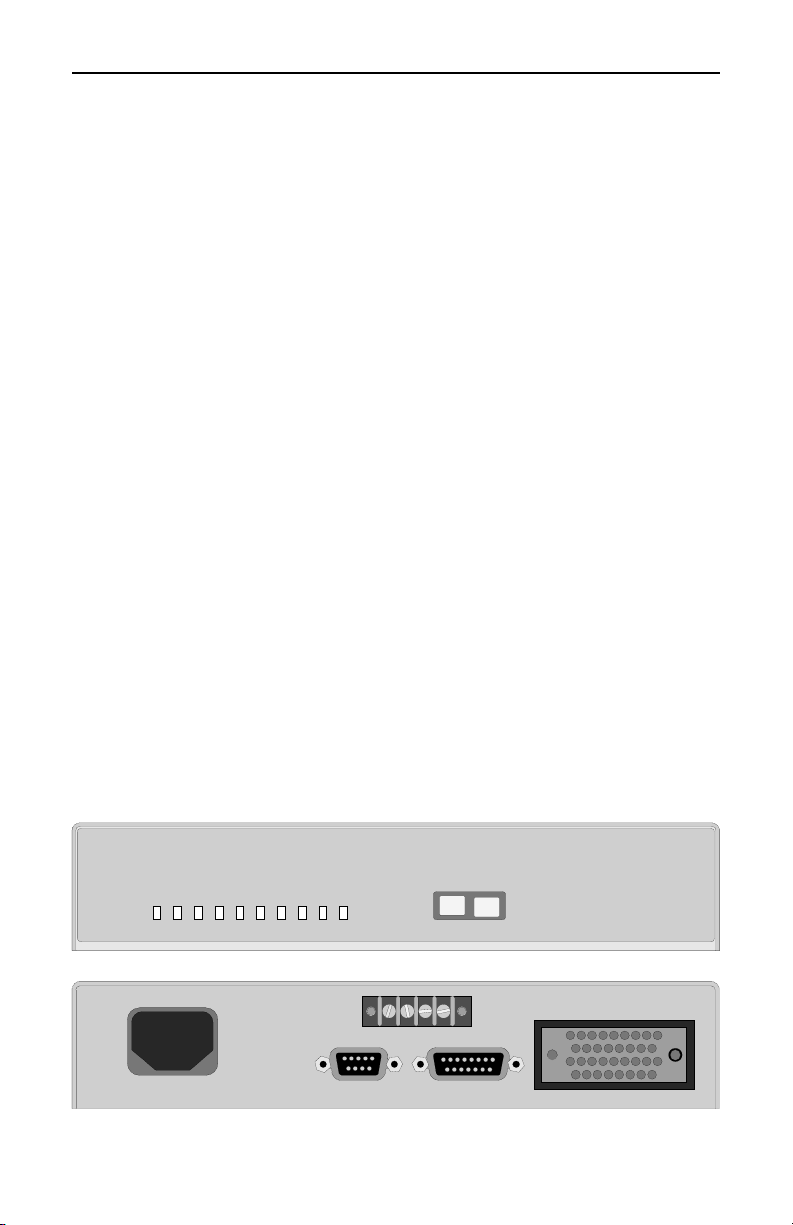
CHAPTER 2 - SETUP AND INSTALLATION
Installation
Set the switches to match the required configurations based on the
diagrams below. The cabling between each device and the interface
converter must be terminated with male connectors. J1 is the V.35
interface, J2 is the X.21 interface and J3 is the V.24 low speed asynchronous interface. The 4 position terminal block is for the G.703 line connection. The IEC connector is provided to interface to the power plug required in the country of use. Insure the 110/220VAC switch is set correctly for the line voltage in use prior to applying power to the interface
converter.
Selection of DTE/DCE
To connect a terminal type device (DTE) to the 2072 (CTS IC-G.703),
connect the Terminal to J1 or J2 and move SW1, SW2, and SW3 to the
rear of the unit toward the connectors (DCE position).
To connect a Modem type device (DCE) to the 2072 (CTS IC-G.703),
connect the Modem to J1 or J2 and move SW1, SW2, and SW3 to the
front of the unit away from the connectors (DTE position).
Equipment Grounding
JP7 provides grounding interconnection in those systems requiring a
connection between Frame Ground and Signal Ground. If signal ground
and chassis ground interconnection is desired, install the jumper on JP7.
LED Indicators
The Following LED indicators are provided for diagnostics: Power (PW),
Transmit Data (TD), Receive Data (RD), Loss of Signal (LOS), Digital
Loopback (DL), Analog Loopback (AL), Test (TST), Remote Loopback
(RLB), Error (ERR) and Sync (SYN).
Front Panel Loop Back Buttons
The Digital Loop and Analog Loop buttons are provided to enable and
disable the testing and loopback features.
2-1
Page 8

180001UA
Data Rate (SW5-3,4)
Selection of data rates is provided by switch 5, positions 3 and 4. The
following chart summarizes the available:
SW5-3 SW5-4 Rate
ON ON 48Kbps
OFF ON 56Kbps
ON OFF 64Kbps
OFF OFF N/A
Control Lead Pass Through / Async Channel (SW5-2)
Selection of the asynchronous service channel or a control lead pass
through for 48K and 56Kbps rate selection is provided by SW5 pos 2. If
an asynchronous 1200 bps service channel is desired, set SW5-2 to ON.
If it is desired to pass the RTS when DCE is selected or the DCD when
DTE is selected to the remote end, set SW5-2 to OFF. The passed
control lead will be presented at the far end as an RTS if the IC-G.703 is
configured as a DTE or DCD if configured as DCE. This option must
match at both ends of the circuit.
Clear to Send (CTS) Control (SW4-6)
Selection of the source for CTS is via Switch 4 pos 6. To force the CTS to
active regardless of RTS activity, set SW4-6 to
CTS to follow RTS then set SW4-6 to
OFFOFF
OFF. This circuit is only operational
OFFOFF
when the 2072 (CTS IC-G.703) is configured as a DCE.
ONON
ON. If it is desired to allow
ONON
Auto Remote Digital Loop Enable (SW5-5)
To enable automatic Remote Digital Loopback when upon detection of the
BERT test pattern set Switch 5 pos 5 to
to ignore the test pattern when received set Switch 5 pos 5 to
ONON
ON.To configure the IC-G.703 unit
ONON
OFFOFF
OFF.
OFFOFF
Loss of Signal or Control Lead to Carrier Detect (SW5-1)
Selection of the source for Carrier Detect (CD) is via Switch 5 pos 1. If you
want the remote units selected control lead to appear on the CD interface
signal leads of the local units, set SW5-1 to
ONON
ON. If it is desired to have the
ONON
Loss Of Signal (LOS) on the CD interface signal leads, then set SW5-1 to
OFFOFF
OFF.
OFFOFF
MARK Polarity (JP5, JP6)
JP5 and JP6 select the polarity of the G.703 signal when the X.21 or V.35
signal is in a MARK condition. If you require MARK to be a
G.703 interface, place the header for both JP5 & JP6 on pins 1 & 2.
2-2
ZEROZERO
ZERO on the
ZEROZERO
Page 9

TX TIMING
DTE
TX BUFFER
RX BUFFER
RX TIMING
RX DATA
RX DATA
TX DATA
PCM
RX TIMING
TX TIMING
TX DATA
180001UA
Looking from the front of the unit this is on the right two pins of both
jumpers. If you require MARK to be a
the header for both JP5 & JP6 on pins 2 & 3. Looking from the front of the
unit this is on the left two pins of both jumpers.
ONEONE
ONE on the G.703 interface, place
ONEONE
Secondary Async Port CTS Forced or Follows RTS (JP4)
JP4 determines the source of the CTS signal on J3, the asynchronous
service port. To force the CTS to constant active, install the header on
JP4 pins 2 & 3. For CTS to follow RTS install the header on JP4 pins
1 & 2.
Clocking Modes (SW4-1,2,3,4,5)
Clocking mode selection is provided by Switch 4, positions 1 through 5.
Only one switch position should be set to OFF at any timeOnly one switch position should be set to OFF at any time
Only one switch position should be set to OFF at any time.
Only one switch position should be set to OFF at any timeOnly one switch position should be set to OFF at any time
Selecting more than one mode may result in erratic operation of the 2072
(CTS IC-G.703).
The G.703 Co-directional interface specification requires that the Data and
Clock will be provided by the same source. The 2072 (CTS IC-G.703) will
provide a clock for the data it sends to the central office PCM link. The
Central Office provides the clock for the data coming from the Central
Office on the PCM link to the 2072 (CTS IC-G.703). This arrangement is
fixed in the hardware and cannot be modified.
Clocking on the V.35 and X.21 interface however is very flexible and can be
configured to meet any need the user has. The follow descriptions along
with the diagrams explain all of the possible clocking modes available to
chose from.
Mode 1 (SW4-1
The 2072 (CTS IC-G.703) provides both receive and transmit clock to a
DTE device connected on the V.35 or X.21 interface. The receive clock
provided on the PCM channel is used to generate all outgoing clocking.
Data passes through both the TX BUFFER and the RX BUFFER using the
PCM RX TIMING for both input and output clocks.
OFF, OFF,
OFF, 2, 3, 4, 5
OFF, OFF,
ONON
ON)
ONON
2-3
Page 10

TX TIMING
Ext TX TIMING
DCE
TX BUFFER
RX BUFFER
TX DATA
RX TIMING
RX DATA
RX DATA
TX DATA
PCM
RX TIMING
TX TIMING
DCE
TX BUFFER
RX BUFFER
TX DATA
RX DATA
RX DATA
TX DATA
PCM
RX TIMING
SIGNAL TIMING
180001UA
Mode 2 (SW4- 2
The 2072 (CTS IC-G.703) gets its receive clock from a DCE device and
gives an external transmit clock to the DCE device connected on the V.35
interface. The receive clock provided on the PCM channel is used to
generate all outgoing clocking. Data passes through the RX BUFFER
using the RX TIMING for both input and output clocks. Data passes
through the TX BUFFER using the DCE TX TIMING for the input clock and
PCM RX TIMING for the output clock. This mode is not available for X.21.
Mode 3 (SW4-3
The 2072 (CTS IC-G.703) gets the Signal Timing from the X.21 DCE device
connected on the DB-15 interface. The receive clock provided by the PCM
channel is used to generate transmit clock for data going to the PCM
interface. Data passes through the RX BUFFER using the PCM RX TIMING
for the input clock and Signal Timing from the X.21 interface for the output
clock. Data passes through the TX BUFFER using the Signal Timing from
the X.21 interface for the input clock and PCM TX TIMING for the output
clock.
OFF OFF
OFF 1, 3, 4, 5
OFF OFF
OFF OFF
OFF 1, 2, 4, 5
OFF OFF
ONON
ON)
ONON
X.21 ONLYX.21 ONLY
ONON
ON)
X.21 ONLY
ONON
X.21 ONLYX.21 ONLY
Mode 4 (SW4-4
The 2072 (CTS IC-G.703) gets an external transmit clock from the DTE
device and gives a receive clock to the DTE device connected on the V.35
interface. The receive clock provided on the PCM channel is used to
OFF OFF
OFF 1, 2, 3, 5
OFF OFF
ONON
ON)
ONON
2-4
Page 11

180001UA
Ext TX TIMING
DTE
TX BUFFER
RX BUFFER
TX DATA
RX TIMING
RX DATA
RX DATA
TX DATA
PCM
TX TIMING
RX TIMING
TX TIMING
DTE
TX BUFFER
RX BUFFER
TX DATA
RX TIMING
RX DATA
RX DATA
TX DATA
PCM
RX TIMING
TX TIMING
TX TIMING
generate the receive clock provided to the V.35 interface. The external
transmit clock provided on the V.35 interface is used to generate the
transmit clock provided to the PCM channel. This mode is not available for
X.21.
Mode 5 (SW4-5
OFF OFF
OFF 1, 2, 3, 4
OFF OFF
ONON
ON)
ONON
The 2072 (CTS IC-G.703) gives both the receive and transmit clock to the
DTE connected on the V.35 interface. The receive clock provided on the
PCM channel is used to generate the receive clock provided to the V.35
interface. An internal time base is used to generate all transmit clocks.
This mode is not available for X.21.
OSC.
Line Terminal Block
The terminal block on the rear panel of the 2072 (CTS IC-G.703) is used to
connect to the G.703 PCM system. The input from the G.703 system
connect to the terminals labeled RX. The output from the 2072 (CTS ICG.703) to the G.703 system come from the terminals labeled TX. Both
input and output are transformer coupled and are not polarity sensitive.
Factory Test Straps
The Factory Test Straps JP1, JP2 and JP3 must be installed for proper
operation of the interface converter.
2-5
Page 12

180001UA
p
quip
p
APPENDIX
TECHNICAL SPECIFICATIONS
Applications
V.35 or X.21 to G.703 Co-Directional
interface and rate conversion
Capacity
One Channel V.35 or X.21 to G.703
Data Format
Data Coding: Synchronous
Data Rates
48Kbps, 56Kbps and 64Kbps
Electrical Interface
V.35 or X.21 and G.703
V.35 Physical Interface
V.35 on a Female M-34 Connector
X.21 Physical Interface
X.21 on a Female DB-15 Connector
G.703 Physical Interface
G.703 Co-Directional Interface on
a 4 position Terminal Block
Enclosure
Metal: Aluminum
Approvals
CE Pending
V.35 or X.21
48, 56 or 64Kb
Data
s
Front Panel
Indicators:....Power, TD, RD,
Switches: ..... Loop Back
Power Requirements
100-120/200-240VAC, 50 to 60Hz,
0.25/0.16A, Switch Selectable
Environmental
Oper Temp:..... 32° to 122°F (0° to
Rel Humidity: ... Up to 90% non-
Altitude:........... 0 t o 10,000 feet
Dimensions
Height: .... 1.75 inches (4.44 cm)
Width: .....8.90 inches (22.60 cm)
Length: ...10.00 inches (25.40 cm)
Weight
2.25 lbs (1.02 Kg)
Warranty
Two Years, Return to Factory
G.703
CoDirectional
s Data
64Kb
LOS, DL, AL, TST,
RLB, ERR, SYN
50°C)
condensing
Central Office
PCM E
ment
2072
Typical Application
2-6
Page 13

180001UA
Power
TD
RD
LOS
DL
AL
TS T
RLB
ERR
SYN
PN-1 80010B
SW5
Analog Loop (IN)
Digital Loop (IN)
Data Rate SW5
3
4
Rate
ON
ON
48K
OFF
ON
56K
ON
OFF
64K
SW4
123456
Clocking Mode 1 = OFF
Clocking Mode 2 = OFF
Clocking Mode 3 = OFF
Clocking Mode 4 = OFF
Clocking Mode 5 = OFF
Force CTS=ON / Follow RTS= OFF
ONOFF
ONE
Only
OF F
Can be
JP 5
MARK = 1
123
MARK = 0
at any time!
123
MARK = 1
MARK = 0
JP 6
123456
CD from Cnt Lead = ON / CD from LOS = OFF
Async Service Chan Available = ON / Cntl Lead Available = OFF
Data Rate
Enable Remote Lo o p = ON / D is ab le R L = O FF
Not Use d
ONOFF
JP3 JP2
Facto r y Test St rap s Must be Instal l ed
for Unit To Operate Corre ct l y
JP1
Connect Signal to
Chassis Ground
DCEDTE
SW1
SW2
SW3
Async S er vice
Channel
RTS/CTS
Forced CT S
3
2
1
J1
V.35
A-1
J2
X.21
JP 4
J3
V.24
JP7
Page 14

180001UA
g
g
g
Transmit(B) (from DTE)
Control(B) (from DTE)
Receive(B) (from DCE)
Indication(B) (from DCE)
nal Timing(B) (from DCE)
Si
Data Set Ready (from DCE)
Request to Send (from DTE)
Clear T o Send (from DCE)
V.24 Asynchronous Interface Pins Supported
BSGFCDL R
AFGE
1
9
10
11
12
13
14
15
Shield (common)
2
Transmit(A) (from DTE)
Control(A) (from DTE)
3
Receive(A) (from DCE)
4
Indication(A) (from DCE)
5
Si
nal Timing(A) (from DCE)
6
7
8
GND (common)
X.21 Interface Pins Supported
Data Carrier Detect (from DCE)
CTS
D
DSR
RTSHDTR
C
6
7
8
9
RD(A)VRT(A)
RD(B)
J N T
TD(A)
K
P
TD(B)WETT(B)AATT(B)
RT(B)
ETT(A)YTT(A)
U
S
1
Transmit Data (from DTE)
2
Receive Data (from DCE)
3
4
5
Si
nal Ground (common)
Z DD JJ
BB FF LL
X
CC HH MM
EE KKM
NN
V.35 Interface Pins Supported
RATING:
110/220
50/60Hz
250mA/160mA
RX TX
J3 J2 J1
Rear Panel
A-2
Page 15

Page 16

B
7622 Rickenbacker Drive
Gaithersburg, MD 20879
Sales: 301 975-1000 Support: 301 975-1007
Web Address: http://www.patton.com
 Loading...