

Page 1

Copyright 2024 PassMark® Software Page 1
MemTest86 User Manual
Version 10.7
Page 2

Copyright 2024 PassMark® Software Page 2
Table of Contents
1 Introduction ......................................................................................................................................................3
1.1 Memory Reliability ...................................................................................................................................3
1.2 MemTest86 Overview ...............................................................................................................................3
1.3 Compatibility ............................................................................................................................................3
1.3.1 UEFI .....................................................................................................................................................3
2 Setup and Use ...................................................................................................................................................5
2.1 Boot-disk Creation in Windows ................................................................................................................6
2.2 Boot-disk Creation in Linux .......................................................................................................................6
2.3 Boot-disk Creation in Mac ........................................................................................................................6
2.4 Setting up Network (PXE) Boot .................................................................................................................8
2.4.1 Configuring a PXE Server on CentOS 7 ................................................................................................8
2.4.2 Configuring Serva for MemTest86 PXE Boot .......................................................................................9
2.5 Using MemTest86 .................................................................................................................................. 14
2.5.1 Booting MemTest86 via USB ............................................................................................................ 14
2.5.2 Booting MemTest86 via Grub .......................................................................................................... 14
2.5.3 Booting MemTest86 via Network (PXE) ........................................................................................... 19
2.5.4 Booting MemTest86 via Serial Console ............................................................................................ 19
2.5.5 MemTest86 Splash Screen ............................................................................................................... 20
2.5.6 Main Menu ...................................................................................................................................... 21
2.5.7 Configuration File (Pro version only) ................................................................................................ 30
2.5.8 Testing .............................................................................................................................................. 39
2.5.9 Test Results/Reports ........................................................................................................................ 40
2.5.10 DIMM / DRAM chip error decoding (Pro & Site Edition only) ..................................................... 43
2.5.11 Troubleshooting MemTest86 Problems ....................................................................................... 46
3 Troubleshooting Memory Errors ................................................................................................................... 47
3.1 Hammer Test (Test 13) Errors ................................................................................................................ 47
3.2 DMA Test (Test 14) Errors ...................................................................................................................... 48
3.3 ECC Errors .............................................................................................................................................. 49
4 Repairing Memory Faults ............................................................................................................................... 50
4.1 Anti-Static Handling Procedures ............................................................................................................ 50
4.2 Re-Seating Memory Modules ................................................................................................................ 50
4.3 Replacing Modules ................................................................................................................................ 50
4.4 Error Validity .......................................................................................................................................... 51
5 Over Clocking ................................................................................................................................................. 52
5.1 Background ............................................................................................................................................ 52
5.2 Operating Margins ................................................................................................................................. 52
5.3 Using MemTest86 for Over Clocking ..................................................................................................... 52
Appendices ............................................................................................................................................................ 55
Appendix A. Technical Information .................................................................................................................... 55
Appendix B. Product Support ............................................................................................................................ 67
Appendix C. Change Log .................................................................................................................................... 70
Appendix D. Acknowledgments ....................................................................................................................... 103
Page 3

Copyright 2024 PassMark® Software Page 3
1 Introduction
1.1 Memory Reliability
Properly functioning memory is critical for reliable operation of any computing device. Few users fully
understand the risks associated with memory errors. Because devices typically do not have any mechanisms for
detecting memory errors, confusing and potentially disastrous consequences can result from these undetected
memory problems. Memory errors will often cause erratic behavior with software applications that can
mysteriously fail. The most serious risk from memory errors, however, is corruption of data that manages how
information is stored on disk. In most cases, this type of corruption will cause one or more files to be lost. There
are cases where a memory error can cause the loss of the entire contents of your hard disk. Periodic testing of
memory with a rigorous and thorough memory test will greatly reduce the risk of problems and data loss due to
memory errors.
1.2 MemTest86 Overview
Memory errors are often pattern sensitive and may be very intermittent. Detecting these errors is technically
challenging and is an imperfect science. MemTest86 uses advanced algorithms that have been refined for more
than 20 years. These testing techniques are highly effective at detecting difficult to find memory errors. In
addition, MemTest86 has the capability to test all available memory.
Memory testing programs execute from memory and therefore are not able to test the memory that is
occupied by the test program itself. MemTest86, due to UEFI platform limitations, is unable to remap itself to
different portions of memory in order to run tests in the section of memory it was occupying. The UEFI
firmware itself also takes up some space compared to a traditional BIOS.
1.3 Compatibility
MemTest86 is designed to work with all processors using the Intel/AMD x86 and x86-64 architecture, as well as
the ARM64 architecture, running on UEFI systems. Most newer systems are able to run the UEFI version of
MemTest86.
MemTest86 is able to test all types of memory; there is no need for MemTest86 to know what type of memory
it is testing. MemTest86 attempts to detect and display information about the hardware it is testing but this
information is not used during testing.
Since MemTest86 is a standalone program, it does not require any operating system support for execution. It
can be used with any PC regardless of what operating system, if any, is installed.
MemTest86 is multi-threaded and is able to concurrently use multiple CPUs to test memory. It may, however, be
limited by the lack of multiprocessor support in the underlying UEFI firmware.
1.3.1 UEFI
For UEFI systems, multiprocessor support is dependent on the multiprocessor services provided by the UEFI
firmware. On older UEFI systems, the multiprocessor support can be limited or incomplete, causing issues such
Page 4

Copyright 2024 PassMark® Software Page 4
as a reduced number of CPU cores available for testing or even program freeze when attempting to run on
other CPU cores. It is recommended that MemTest86 is run on only one CPU core if it fails to run on multiple
CPU cores.
Page 5

Copyright 2024 PassMark® Software Page 5
2 Setup and Use
MemTest86 supports booting from the UEFI platform. When booting from UEFI, MemTest86 has access to
additional services not available in BIOS including:
• Native 64-bit support
• No longer requires the use of the PAE workaround to access more than 4GB of memory. (PAE = Physical
Address Extension)
• Improved multi-threading support, where supported by the underlying UEFI system
• Option to disable CPU memory caching for all or individual tests
• Graphical interface with mouse input where supported by the underlying UEFI system
• Improved USB keyboard support, including systems that fail to emulate IO Port 64/60 correctly (eg. Mac
USB keyboards)
• Reporting of configured RAM parameters including clock speed, timings, channel mode and voltages
(limited to supported chipsets, ongoing development)
• Reporting of detailed RAM SPD information including timings, clock speeds, vendor names and much
more
◦ Support for DDR5 RAM (and associated hardware), including retrieval and reporting of DDR5-
specific SPD details. This includes DDR5 RAM that support Intel XMP 3.0 profiles.
• ECC error reporting (limited to supported chipsets, ongoing development)
◦ Reporting of ECC capabilities and operation mode
◦ Reporting of detected and corrected ECC errors
◦ Injection of ECC errors for test purposes (limited hardware only)
• DIMM-level/chip-level error detection (limited to supported chipsets, ongoing development)
◦ Per-module/per-chip error tracking and reporting
◦ Results summarized in a simplified graphical display/HTML report
• Real-time DIMM temperature reporting (limited to supported chipsets, ongoing development)
• Support for storing logs and reports to disk/network. In all prior MemTest86 releases, there was no disk
or network support.
• Support for network PXE boot for scalable, diskless deployment
• Full test automation via configuration file
• Secure Boot signed by Microsoft for ensuring software integrity
MemTest86 can boot from USB flash drive or, with Linux systems, by the boot loader (for example, LILO or
Grub). Any Windows, Linux or Mac system may be used to create the USB flash drive. Once a MemTest86 boot
disk has been created, it may be used on any x86 (PC) computer with a USB flash drive.
MemTest86 (Site Edition only) also supports diskless booting via PXE network boot. A DHCP/PXE server must be
present on the network for PXE boot-enabled client machines to obtain the MemTest86 image via the network.
Page 6

Copyright 2024 PassMark® Software Page 6
2.1 Boot-disk Creation in Windows
1. Download the MemTest86 USB image zip file.
2. Extract the contents of the zip file to a directory
3. Plug in the USB drive
4. Launch the ImageUSB application included in the zip file
5. Select your USB drive from the list (Step 1).
6. Select 'Write image to USB drive' (Step 2)
7. If it is not already selected, select the included image file (Step 3).
8. Click 'Write' (Step 4).
9. After accepting a few more prompts this should give you a working bootable USB drive
2.2 Boot-disk Creation in Linux
1. Download the MemTest86 USB image.
2. Unzip the package (unzip memtest86-usb.zip). An image file and a readme.txt file will be created in the
current directory.
3. Plug in the USB drive
4. Determine which device the USB drive is assigned as (eg. /dev/sdc) by opening the Terminal and typing
the following command:
lsblk -p -o NAME,VENDOR,MODEL,SIZE,TYPE,SERIAL
5. As root, use the 'dd' command to write the image to the USB drive. For example,
sudo dd if=memtest86-usb.img of=<dev> conv=fsync status=progress
where <dev> is the device the USB key is assigned to obtained from the previous command. Use the
base device (ie. /dev/sdc) not a partition designation (ie. /dev/sdc1).
**Warning** All data on the USB key will be lost. Make sure that the device used in the dd command
above is correct.
2.3 Boot-disk Creation in Mac
1. Download the MemTest86 USB image.
2. Unzip the package (unzip memtest86-usb.zip). An image file and a readme.txt file will be created in the
current directory.
3. Plug in the USB drive
4. Determine which device the USB drive is assigned as by opening the Terminal and typing the following
command:
diskutil list
5. Unmount all volumes on the USB drive by typing the following command:
Page 7

Copyright 2024 PassMark® Software Page 7
diskutil unmountDisk [device name]
6. As root, use the 'dd' command to write the image to the USB drive. For example,
sudo dd if=memtest86-usb.img of=<dev> conv=sync
where <dev> is the device the USB key is assigned to obtained from the previous command. Use the
base device (ie. /dev/disk1) not a partition designation (ie. /dev/disk1s1).
**Warning** All data on the USB key will be lost. Make sure that the device used in the dd command
above is correct.
Page 8

Copyright 2024 PassMark® Software Page 8
2.4 Setting up Network (PXE) Boot
MemTest86 (Site Edition only) supports network booting via PXE. In order to configure PXE booting of
MemTest86, a DHCP/PXE server must be present on the network which hosts the MemTest86 boot images to
PXE boot-enabled client machines. Network booting of MemTest86 has been tested successfully with the Linuxbased CentOS (DHCP + TFTP server) and Windows-based Serva PXE Server but other PXE servers should work as
well. For step-by-step instructions, see Configuring a PXE Server on CentOS 7 or Configuring Serva for
MemTest86 PXE Boot. For others, see the manual for your DHCP/PXE server for configuration instructions.
Once the PXE server is configured, extract the files from the MemTest86 Site Edition package to the appropriate
directory for your PXE server configuration. In the PXE server settings, specify the boot image file to
“BOOTX64.efi” for x86-64 clients, “BOOTIA32.efi” for x86 clients, and “BOOTAA64.efi” for ARM64 clients.
The configuration file (mt86.cfg) is supported in PXE boot and can be used to configure and customize
MemTest86. Likewise, report files are supported and can be uploaded to the PXE/TFTP server. Currently, logs
can only be saved on a local disk.
2.4.1 Configuring a PXE Server on CentOS 7
Any Linux distribution that includes TFTP and DHCP server software packages can be configured as a PXE server.
This has been tested successfully on CentOS 7 but other mainstream Linux distributions can be configured as
PXE servers as well. Please consult the documentation for those distributions for setup instructions.
1. Open a terminal session
2. Install the TFTP server by entering the following:
yum install tftp-server xinetd
3. Configure TFTP server by editing /etc/xinetd.d/tftp. In particular, ensure ‘disable’ is set to ‘no’ and
server_args is set appropriately (ie. includes a path to your TFTP server root directory and specifies a
remap file for fixing paths with backslashes).
service tftp
{
socket_type = dgram
protocol = udp
wait = yes
user = root
server = /usr/sbin/in.tftpd
server_args = -c -s -m /var/lib/tftpboot/tftp.remap /var/lib/tftpboot
disable = no
per_source = 11
cps = 100 2
flags = IPv4
}
4. Create the TFTP server root directory. In the following example, the TFTP root directory is
/var/lib/tftpboot
mkdir -p /var/lib/tftpboot
5. Extract MemTest86 Site Edition files to the TFTP server root directory. Ensure read/write permissions
are properly set.
Page 9

Copyright 2024 PassMark® Software Page 9
unzip memtest86-site.tar.gz -d /var/lib/tftpboot
chmod -R 777 /var/lib/tftpboot
6. Install DHCP server by entering the following:
yum install dhcp
7. Configure the DHCP server by editing /etc/dhcpd.conf. In the following example, the the DHCP server
shall provision IP addresses to a local network with subnet 192.168.100.0/24. The DHCP server is
connected to this network via interface eth0 which is assigned a static IP address of 192.168.100.1
option arch code 93 = unsigned integer 16; # RFC4578
allow booting;
allow bootp;
subnet 192.168.100.0 netmask 255.255.255.0 {
interface eth0;
range dynamic-bootp 192.168.100.100 192.168.100.254;
option broadcast-address 192.168.100.255;
option routers 192.168.100.1;
class "pxeclients" {
match if substring (option vendor-class-identifier,0,9) = "PXEClient";
next-server 192.168.100.1;
if option arch = 00:09 { # x86-64 EFI BOOT
filename "BOOTX64.efi";
}
else if option arch = 00:07 { # x86-64 EFI BOOT
filename "BOOTX64.efi";
}
else if option arch = 00:06 { # x86 EFI BOOT
filename "BOOTX32.efi";
}
else if option arch = 00:0b { # ARM64 EFI BOOT
filename "BOOTAA64.efi";
}
else { # legacy BIOS boot
filename "pxelinux.0";
}
}
}
8. Start the TFTP and DHCP servers
service xinetd start
service tftp start
service dhcpd start
2.4.2 Configuring Serva for MemTest86 PXE Boot
Serva is a light-weight but powerful Windows PXE server that bundles all required services (eg. DHCP, TFTP) in
order to support UEFI-based booting. Serva does not require an installation and can be setup in minutes.
Note: MemTest86 PXE Boot has been tested to work with Serva v3.0.0. There has been reports of issues with
uploaded files being truncated to 512 bytes with Serva v3.2.0. Please use v3.0.0 until the issue has been
resolved.
To enable PXE booting of MemTest86, Serva can be configured in one of two ways: Single-Image Boot (for
booting MemTest86 only) or Automated Multi-Image Boot (for configuring multiple boot targets).
Page 10
Copyright 2024 PassMark® Software Page 10
2.4.2.1 Single-Image Boot
Configuring Serva for Single-Image Boot is ideal for servers that require only a simple setup and do not need to
distribute software images other than MemTest86. All necessary settings are configured within the Serva
application and do not require any additional configuration files.
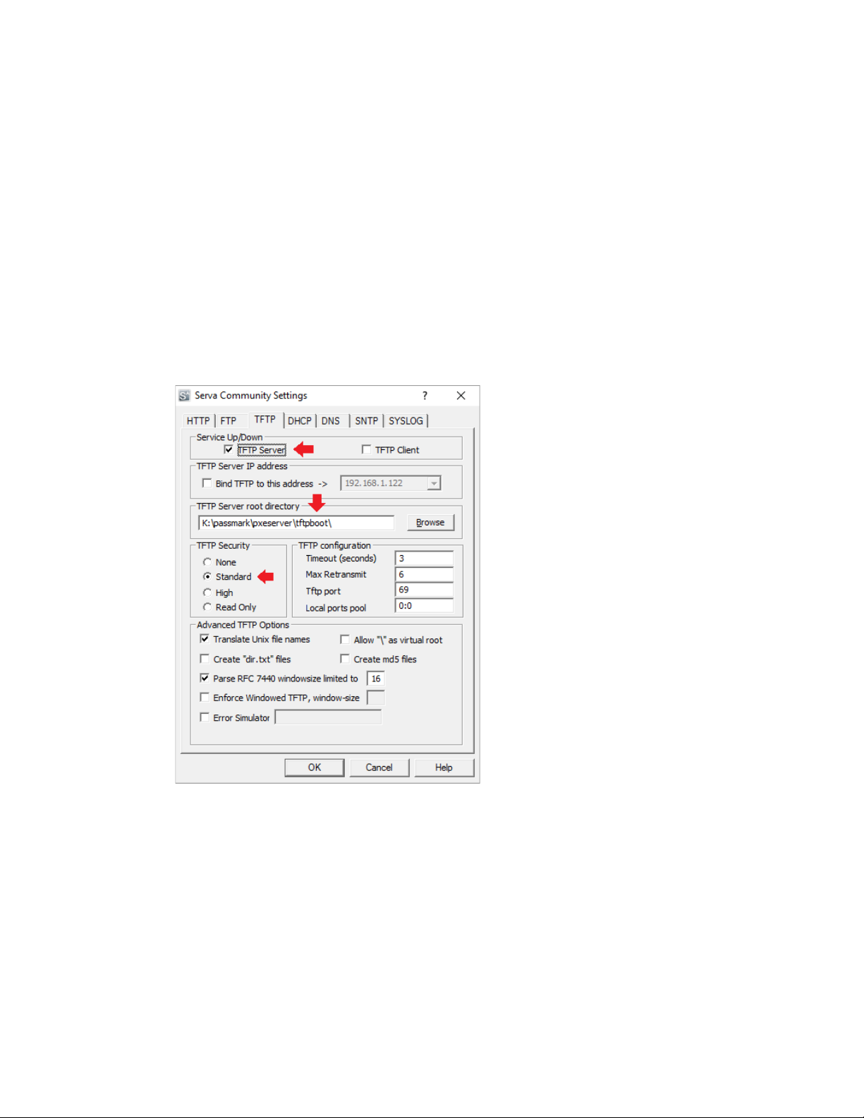
1. Open Serva and select 'Settings'
2. Click on the TFTP tab to setup the TFTP server
a) Ensure that 'TFTP Server' is checked
b) Specify the TFTP root directory. This should be the location where the files in the MemTest86 are to
be extracted.
c) Set the TFTP Security to 'Standard' to allow MemTes86 report files to be uploaded to the server
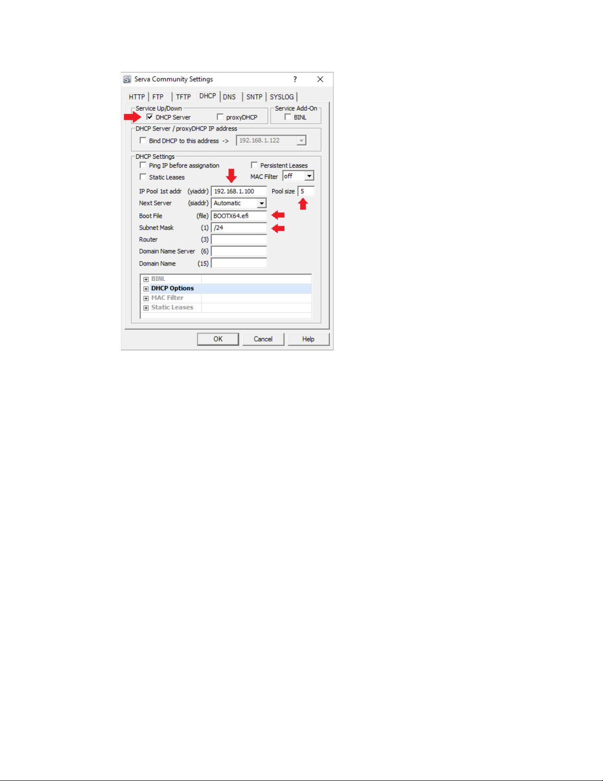
3. Click on the DHCP tab to setup the DHCP server
a) If your network already has a DHCP server, check 'proxyDHCP'. Otherwise, check 'DHCP Server'.
b) If 'DHCP Server' is selected, specify the 'IP Pool 1st Addr', 'Pool size' and 'Subnet Mask' for the DHCP
server.
c) Specify the 'Boot File' to be retrieved by the client. For x86 clients (most systems), enter
'BOOTX64.efi' (64-bit) OR 'BOOTIA32.efi' (32-bit) as the boot file. For ARM64 clients, enter
'BOOTAA64.efi'.
Page 11
Copyright 2024 PassMark® Software Page 11
4. Press OK to save the settings.
5. Extract all files in the MemTest86 package in the folder specified in Step 2b.
6. Close and restart Serva to apply the settings.
2.4.2.2 Automated Multi-Image Boot
Configuring Serva for Automated Multi-Image Boot is ideal for servers that distribute more than one boot
image to PXE clients. Instead of booting the MemTest86 image directly, the client machine is given a menu of
boot images to choose from. This configuration offers the convenience and flexibility of managing multiple boot
images with minimal overhead.
1. Open Serva and select 'Settings'
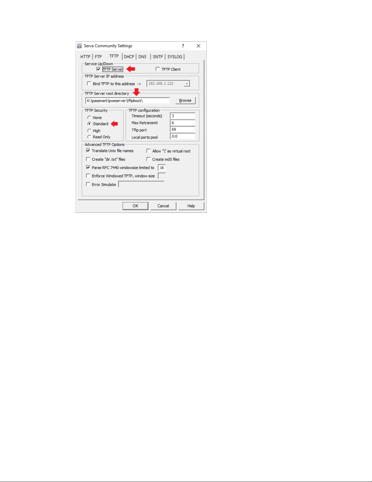
2. Click on the TFTP tab to setup the TFTP server
a) Ensure that 'TFTP Server' is checked
b) Specify the TFTP root directory. This should be the root directory of where all boot images are
stored.
Page 12
Copyright 2024 PassMark® Software Page 12
c) Set the TFTP Security to 'Standard' to allow MemTes86 report files to be uploaded to the server
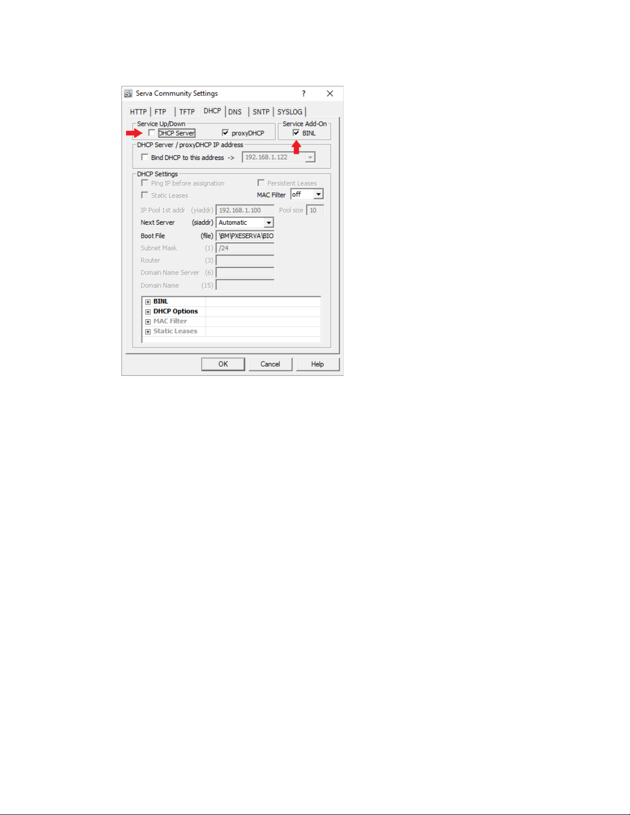
3. Click on the DHCP tab to setup the DHCP server
a) If your network already has a DHCP server, check 'proxyDHCP'. Otherwise, check 'DHCP Server'.
b) If 'DHCP Server' is checked, specify the 'IP Pool 1st Addr', 'Pool size' and 'Subnet Mask' for the DHCP
server.
c) Check 'BINL' to enable automated management of boot images
Page 13
Copyright 2024 PassMark® Software Page 13
4. Press OK to save the settings. Close and restart Serva to apply the settings.
5. After restarting Serva, a directory structure of several folders should have been created in the TFTP root
directory specified in Step 2b. Open the 'NWA_PXE' folder and create a new directory to hold the
MemTest86 files (eg. 'MEMTEST86').
6. Extract all files in the MemTest86 package to the directory created in Step 5.
7. Verify 'ServaAsset.inf' exists in the directory. If not, create and paste the following configuration text in
the file. For more details on the configuration parameters, consult the Serva manual.
[PXESERVA_MENU_ENTRY]
asset = MemTest86
platform = x86
kernel_efi64 = \NWA_PXE\$HEAD_DIR$\BOOTX64.EFI
append_efi64 = TFTPROOT=\NWA_PXE\$HEAD_DIR$
kernel_efi32 = \NWA_PXE\$HEAD_DIR$\BOOTIA32.EFI
append_efi32 = TFTPROOT=\NWA_PXE\$HEAD_DIR$
8. Close and restart Serva to apply the settings.
Page 14

Copyright 2024 PassMark® Software Page 14
2.5 Using MemTest86
2.5.1 Booting MemTest86 via USB
To start MemTest86 insert the USB flash drive into the appropriate slot and restart your computer.
Note: The UEFI BIOS must be configured to boot from the device that MemTest86 is installed
on. Most systems have an optional boot menu that is enabled by pressing a key at startup
(often ESC, F9, F11 or F12). If available, use the boot menu to select the correct drive. Please
consult your motherboard documentation for details.
It may also be possible to boot using USB card reader devices, although compatibility depends
on the device itself and/or motherboard. For optimal compatibility, please use the USB drives
implementing the fastest available standard (eg. USB 3.1) from reputable vendors.
On a Mac, to boot from USB, you need to hold down the ALT / Option key on the Mac keyboard
while powering on the machine.
On newer Macs (from 2018) with the Apple T2 Security Chip, you may need to change the
SecureBoot settings for MemTest86 to boot. Please see the following page for instructions:
https://support.apple.com/en-us/HT208330
All MemTest86 images support booting only in UEFI mode. If your system is unable to boot MemTest86, it is
most likely that either:
1. You have an older system that does not support UEFI
2. Your system supports UEFI but is configured in legacy mode (ie. BIOS)
If (1) is true, you system will not be able to boot MemTest86. You will need to upgrade to a new system that
supports UEFI in order to run MemTest86.
If (2) is true, you will need to go to the BIOS setup and change the necessary settings in order to boot from
UEFI. The actual BIOS setting varies depending on the vendor but it is typically "Legacy Boot", "CSM" or
"Compatibility Support Module".
2.5.2 Booting MemTest86 via Grub
Grub is a popular boot loader that many popular Linux distributions come pre-packaged with, such as Ubuntu
LTS. In our instance, Grub can be used to chainload MemTest86, directly from a local boot disk/partition on the
system.
The following guide provides users with step-by-step instructions on how to configure and use Memtest86 x64
with Grub v2.04 running under Ubuntu 20.04 LTS 64-bit. Please note that the same steps will likely work with
other Linux distributions, however this is the only configuration that has been tested and thus cannot
guarantee compatibility or provide support for other configurations (e.g. different Linux distros, older Grub
Page 15
Copyright 2024 PassMark® Software Page 15
versions etc.) The guide assumes that the user is familiar with Linux operating systems and terminal commands.
2.5.2.1 Pre-requisite: enabling Grub menu during boot
On some Linux distributions such as Ubuntu 20.04 LTS, the Grub boot menu is hidden by default, and skipped
during the boot process. As such, Grub needs to be configured to permanently display its menu, by performing
the following steps:
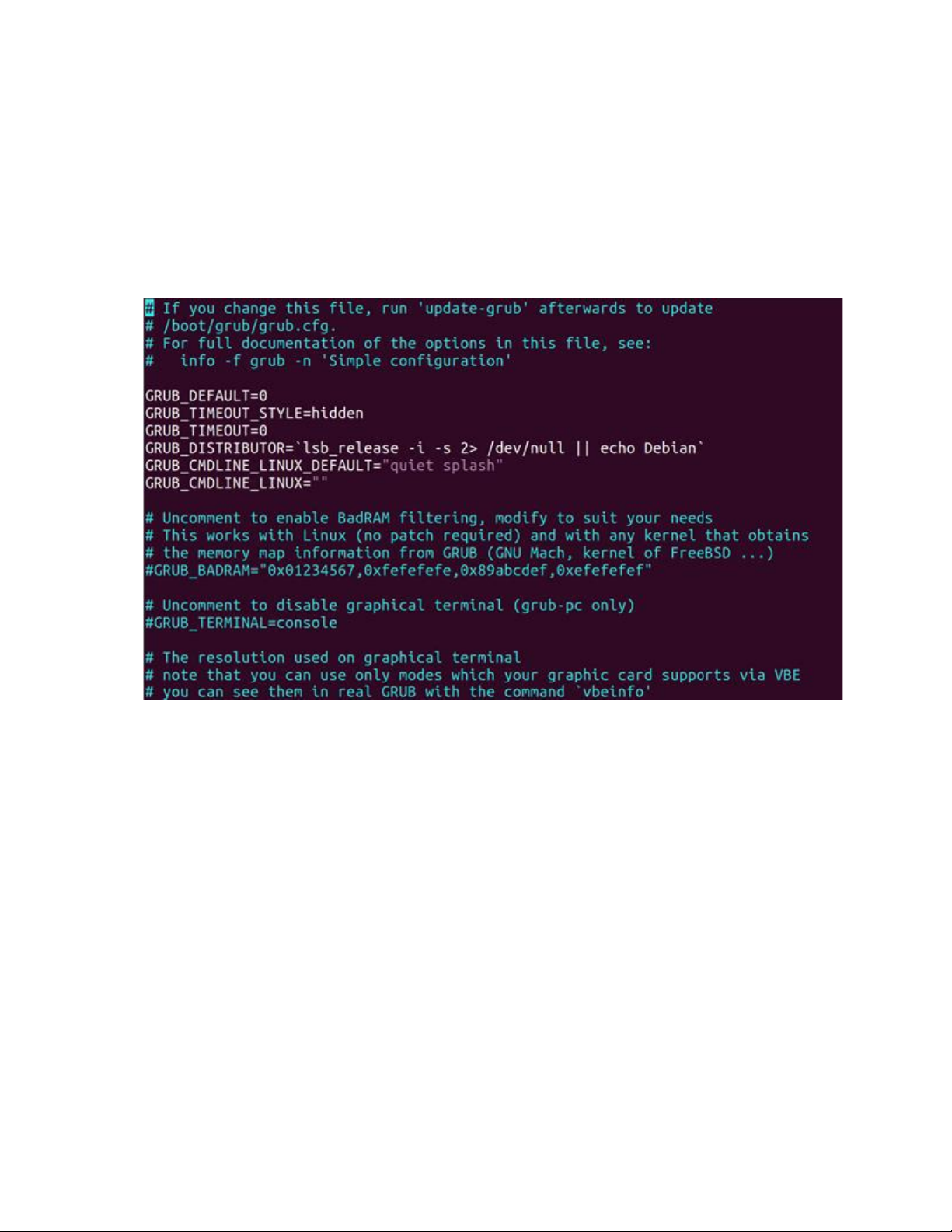
1. Open the file /etc/default/grub with a text editor, you will see the following contents
2. Change the following two lines and save, close the file:
GRUB_TIMEOUT_STYLE=menu
GRUB_TIMEOUT=10
3. Update the grub configuration by running the command below:
sudo update-grub
2.5.2.2 Setup MemTest86 for Grub boot
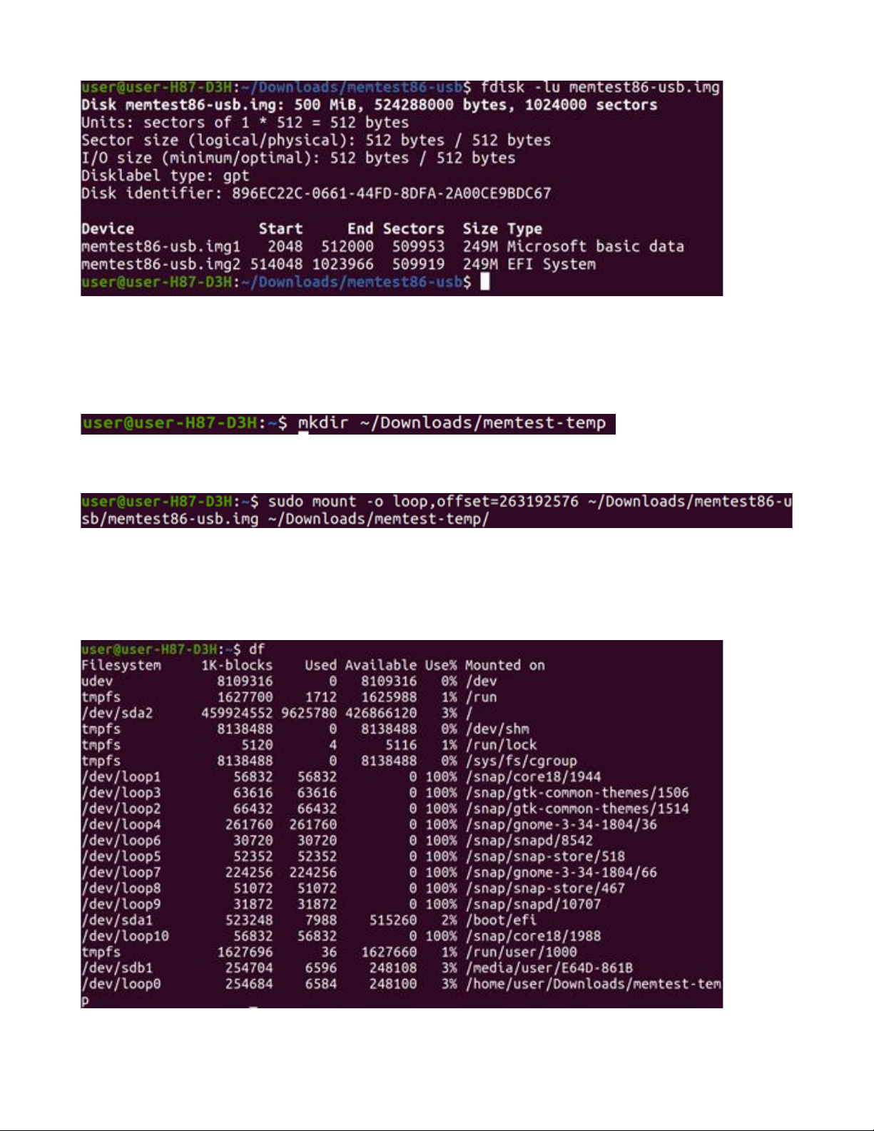
1. Create a boot image from the MemTest86 USB zip file:
Download the MemTest86 USB zip file available from the PassMark website. Unzip it within its current
directory, and then use the built-in fdisk utility to analyze the partition structure and determine the correct
mount point:
Page 16
Copyright 2024 PassMark® Software Page 16
In the screenshot above, the file that needs to be mounted is the memtest86-usb.img2 file, which
contains the EFI boot image. As such, this file is extracted and mounted to a temporary location/folder, using
the below series of commands.
Create a temporary directory using the following command:
Next, mount the image file to the temporary directory chosen earlier, by calculating the correct mount offset
(obtained by multiplying the start – 514048 by 512, the size of each sector, resulting in 263192576):
2. Copy the boot image from the temporary drive to the system EFI partition:
In order to perform this, first locate and confirm the EFI boot drive partition for your local system. This can be
performed by running the df command, and observing the output:
Page 17

Copyright 2024 PassMark® Software Page 17
On this particular system, the EFI boot partition (/boot/efi) is stored under /dev/sda1.
Take note of this directory as it directly corresponds to the disk number, and boot partition the EFI file system is
on, this information will be needed in subsequent steps. In this particular example:
/dev/sdxy
where x corresponds to the disk number. a = disk 0, b = disk 1, etc.
where y corresponds to the partition number. 1 = partition 1, 2 = partition 2, etc.
Now, copy the locally created /EFI/BOOT directory to your system’s EFI boot directory using the following
command:
a. For NVMe drives:
If the EFI boot partition is on a NVMe drive, the above steps will not display the correct partition. Instead, the
following steps are required to get the correct disk and partition:
1) Press "c" on the grub menu to get a command line
2) Enter "ls" to get a list of all the drives. The drive/partitions are all listed as (hd#,gpt#), regardless
of what they are physically. Then list the root using "ls (hd#,gpt#)/", for each drive until you find
the EFI boot partition.
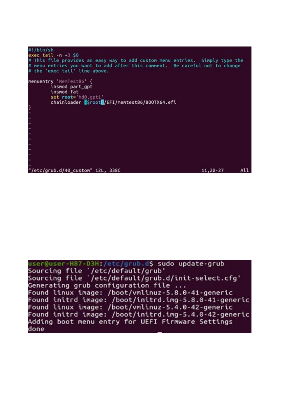
3. Modify the Grub config to add a MemTest86 boot option:
Navigate to the grub config file directory. Below are the contents of the directory on a fresh Ubuntu installation.
In our case we will be editing the 40_custom file. This file is a template that you can use to create additional
entries to be added to the boot menu.
Page 18
Copyright 2024 PassMark® Software Page 18
Open the file in a text editor (with sudo privileges) and add the following text:
Pay attention to the following line:
set root = ‘hd0,gpt1’
Based on your specific environment, edit this line as follows:
hd(x); where (x) = disk number identified in Step 2.
gpt(x); where (x) = partition number identified in Step 2.
Save and close the file.
Finally run the below command to update your grub config, and then reboot your system.
sudo update-grub
Assuming the above steps were successfully performed, the grub bootloader menu should now appear, and
display MemTest86 as an option.
Page 19
Copyright 2024 PassMark® Software Page 19
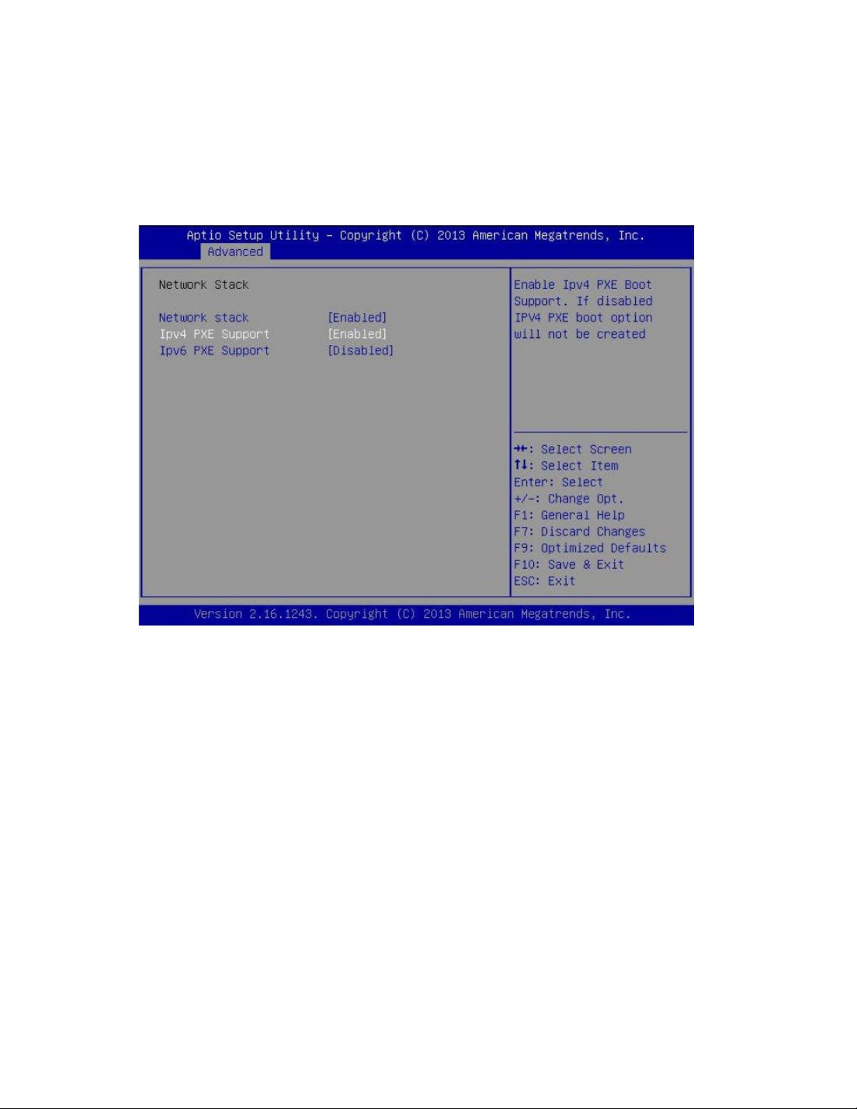
2.5.3 Booting MemTest86 via Network (PXE)
After configuring the PXE Server for MemTest86 deployment, the client machine must also be configured to
boot from network (PXE). In the BIOS setup, ensure that the “UEFI Network Stack” and “IPv4 PXE Support'
features are enabled, similar to the screenshot below.
Once PXE support is enabled, ensure that the network PXE boot option is in the appropriate boot order.
Most systems also have an optional boot menu that is enabled by pressing a key at startup (often ESC, F9, F11
or F12). If available, use the boot menu to select the network PXE boot option. Please consult your
motherboard documentation for details.
2.5.4 Booting MemTest86 via Serial Console
For systems without video support, MemTest86 can run in serial console mode from both UEFI and BIOS
systems. For MemTest86 v4, select option 5 from the menu to enable output to serial console. You will not
need to do anything for MemTest86 v5 or later as it will automatically use the serial console, provided that the
UEFI BIOS has been configured to redirect the console to the serial port. No GUI support is available when using
the serial console so all test configurations must be done using the configuration file.
Page 20
Copyright 2024 PassMark® Software Page 20
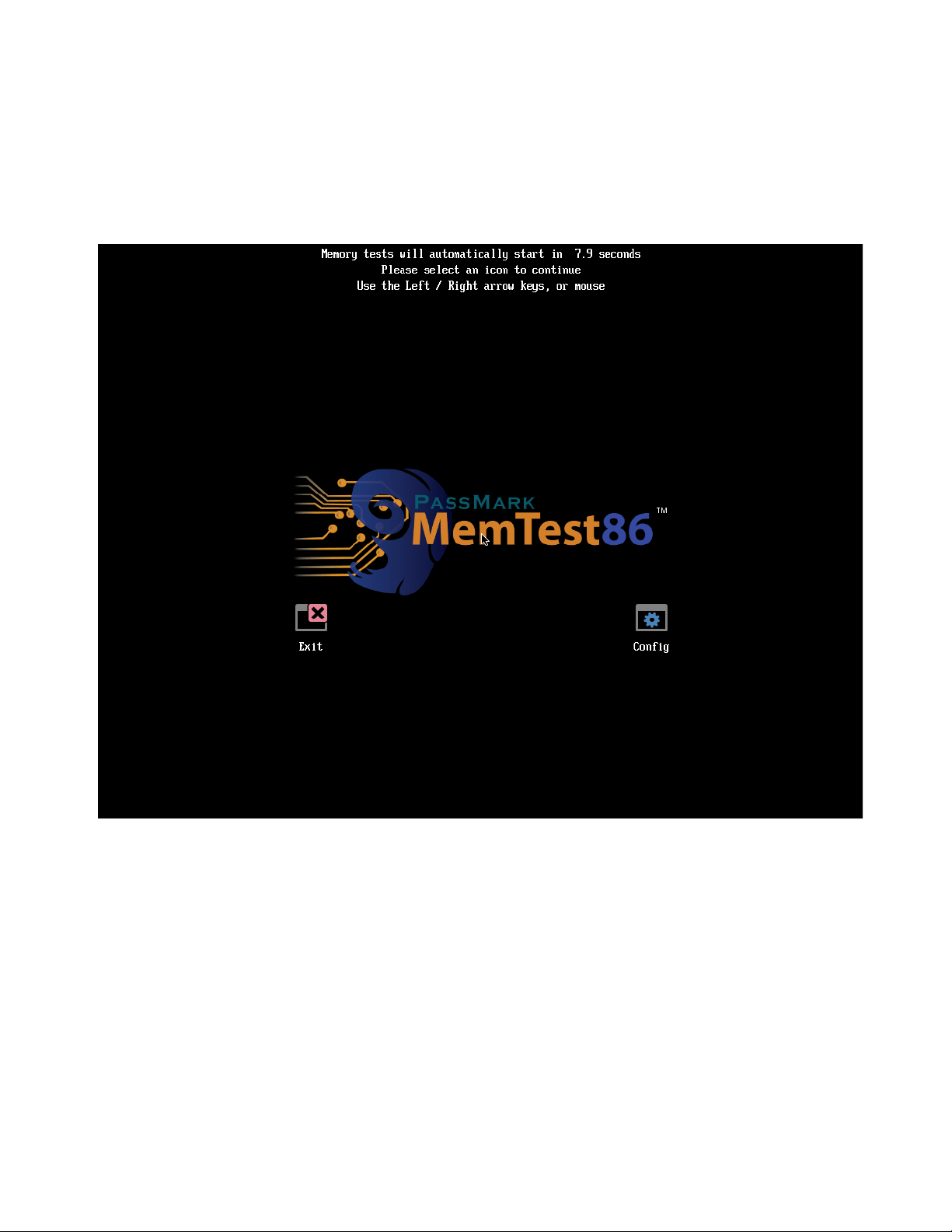
2.5.5 MemTest86 Splash Screen
When MemTest86 boots, a splash screen is displayed with a 10 second countdown timer which when expires,
automatically starts the memory tests with default settings. Pressing a key or moving the mouse shall stop the
timer.
Selecting Exit shall allow the user to reboot, shutdown or exit MemTest86. To configure the memory tests,
select Config and the main menu is displayed. The main menu allows the user to customize the memory test
settings such as the specific tests to execute, address range to test and which CPU core(s) are used in testing.
Page 21
Copyright 2024 PassMark® Software Page 21
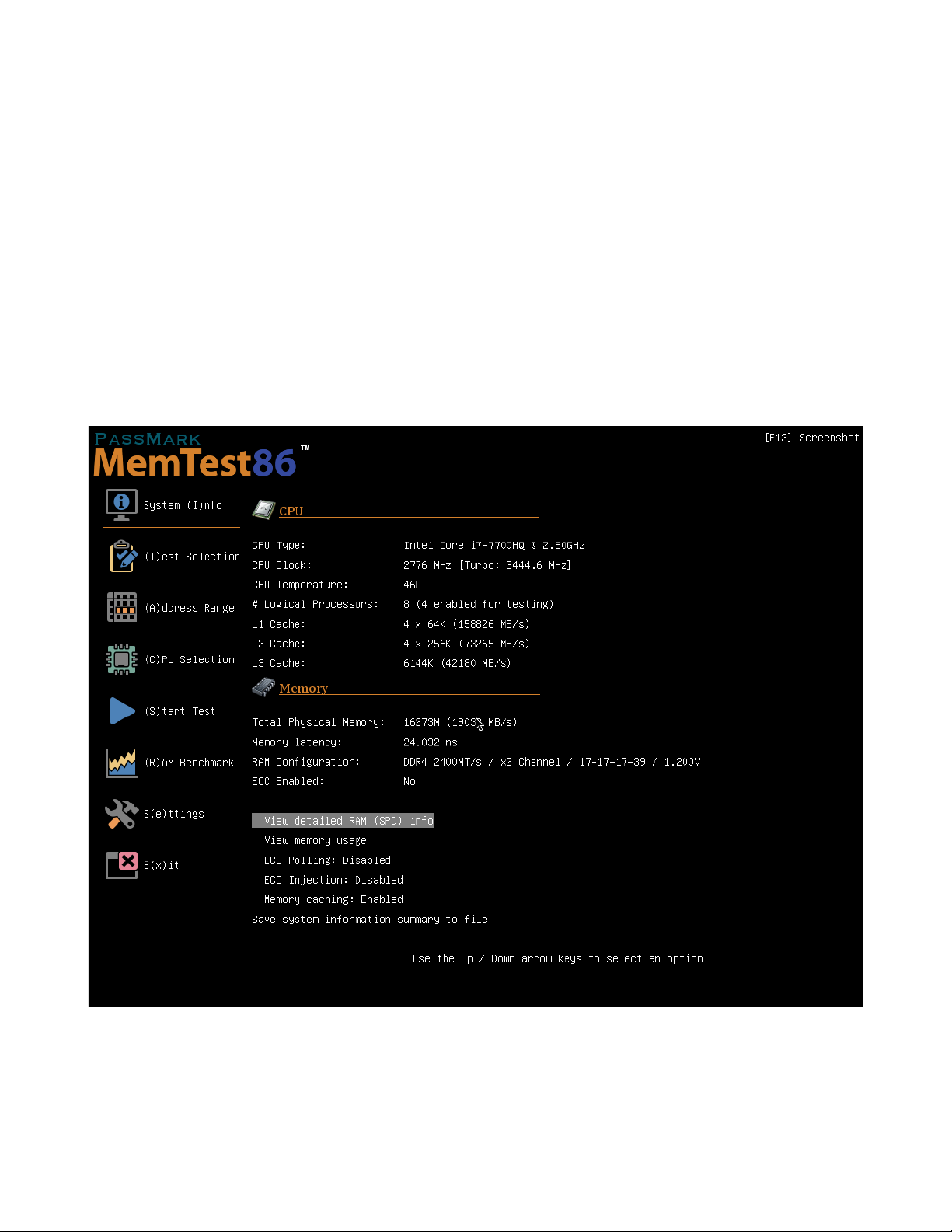
2.5.6 Main Menu
The Main Menu provides a graphical interface for configuring memory test parameters, as well as displaying
information about the system.
A screenshot can be taken and saved to file at any time by pressing F12.
2.5.6.1 System Info
The System Info screen displays the hardware information of the system it is running on, including the
following:
• CPU information, including clock speed, cache information and number of cores
• Memory information, including the total physical memory, RAM configuration and ECC mode
View detailed RAM (SPD) info - displays the SPD information stored in the individual RAM modules. The RAM
SPD information can be saved to a file on disk (Pro version only)
Page 22

Copyright 2024 PassMark® Software Page 22
Note: Retrieving RAM SPD information is highly dependent on the system's motherboard/CPU chipset. Most
common hardware should be supported but for some systems, accessing the SPD modules using the mechanism
required by the chipset may not be supported. If this is the case, please send the MemTest86.log file to
help@passmark.com, along with details of your system. The log file will be analyzed to determine whether the
chipset can be supported in future versions.
View memory usage - displays the system memory address map.
ECC polling : Enabled/Disabled – if ECC detection/correction is supported and enabled, this option
disables/enables periodic checking of any ECC errors that have been detected by the system while the memory
tests are running.
ECC injection: Enabled/Disabled (Pro version only) - if ECC detection/correction is supported/enabled and ECC
injection is supported by the system, this option enables/disables injection of ECC errors to simulate how the
system responds to real ECC errors. ECC errors are injected at the start of each individual test. If ECC injection is
successful, the details of the ECC error shall be reported and displayed on screen as if an actual ECC error was
detected.
Note: Although ECC injection may be supported by your hardware, it may be locked by the BIOS. Some BIOS may
allow you to unlock the ECC injection feature in the BIOS setup. In some cases, however, you may need a
modified BIOS which does not lock the ECC injection feature.
Memory caching: Enabled/Disabled (Pro version only)– disable/enable memory caching when the tests are
running. Warning - disabling memory caching greatly reduces the performance of the entire system, including
screen updates.
Save system information summary to file (Pro version only)- Save the system information to a file on disk
Page 23
Copyright 2024 PassMark® Software Page 23
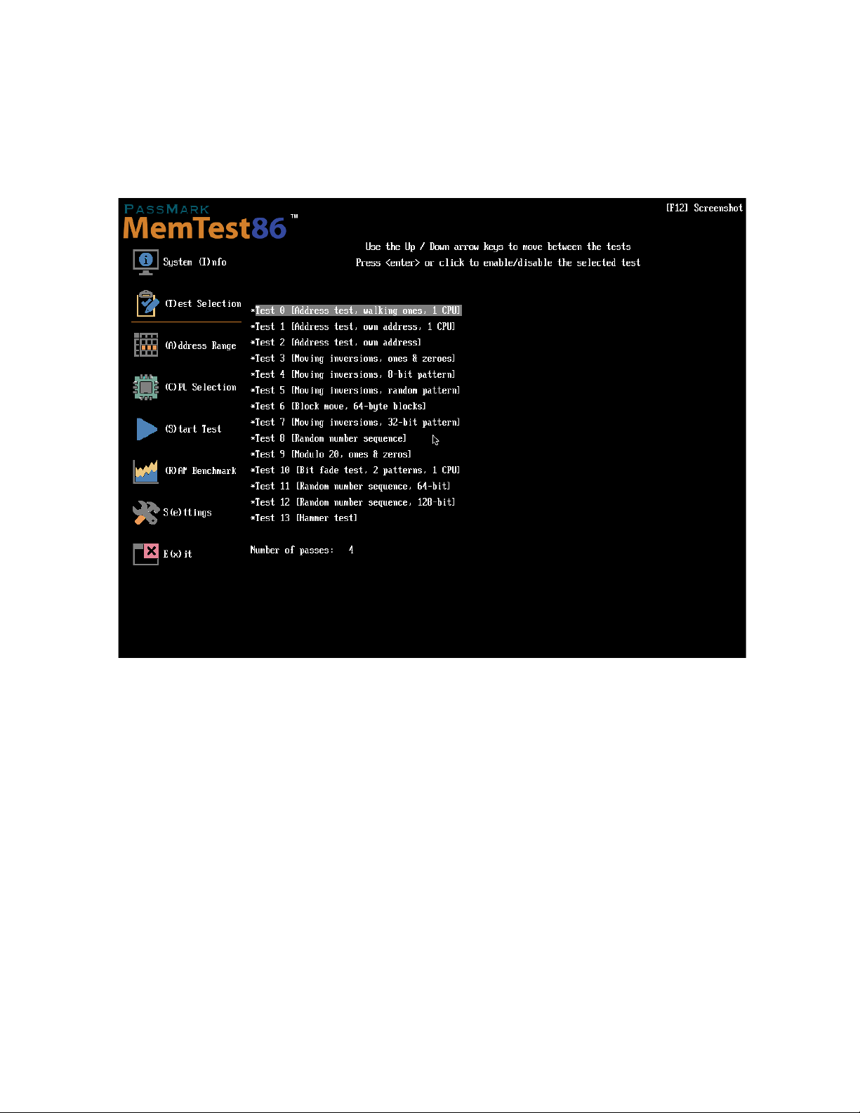
2.5.6.2 Test Selection
The Test Selection screen allows the user to select the test sequence to run, and the number of passes to run
each sequence. See Individual Test Descriptions for a detailed description of each test.
To enable/disable a test, use the up / down arrow keys or mouse to highlight a test, then press enter or click.
Test 11 and 12 are available only in the Pro version.
To change the number of passes, select Number of passes and enter the desired number of passes. (Pro version
only)
Page 24
Copyright 2024 PassMark® Software Page 24
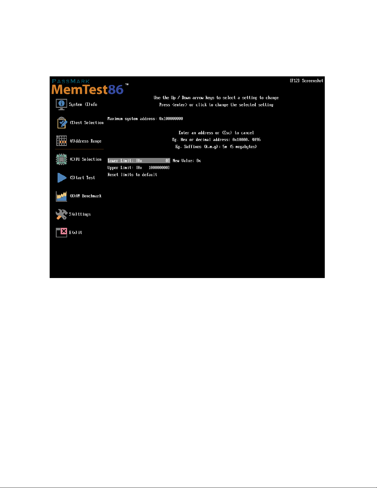
2.5.6.3 Address Range
The Address Range screen allows the user to specify a subset of the total system address map to test.
To change the lower or upper limit of the address range to test, select the appropriate setting and enter a new
value.
To enter a decimal address, enter the address as is.
To enter a hexadecimal address, enter 0x followed by the hex address.
You may also use the suffixes k, m, g to specify kilobyte, megabytes and gigabytes respectively.
Selecting Reset Limits to default will reset the limits to its maximum values.
Page 25
Copyright 2024 PassMark® Software Page 25
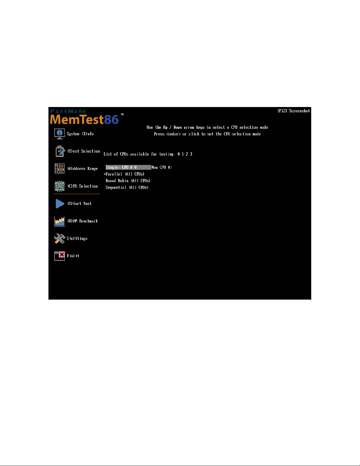
2.5.6.4 CPU Selection
The CPU Selection screen allows the user to specify a single CPU core to test, or cycle through all logical CPU
cores using a selection mode.
In the Free version, the maximum number of logical CPU cores supported in MemTest86 is 16.
In the Pro version, the maximum number of logical CPU cores supported in MemTest86 is 256, but can be
increased to 512 using the MAXCPUS configuration file parameter.
Single - specifies a single CPU core to test, and prompts the user to enter a valid CPU ID number
Parallel - executes the memory tests on all physical (ie. non-hyperthread) CPU cores concurrently, on a set of
non-overlapping memory segments. Memory segments are allocated consecutively to CPU core numbers in
alternating ascending and descending order for each pass.
Round Robin - only one CPU core is running a test at any given time but cycles to the next CPU core in a round
robin fashion after every test
Sequential - only one CPU core is running a test at any given time but cycles to the next CPU after a certain
memory size has been tested by the CPU core.
Page 26
Copyright 2024 PassMark® Software Page 26
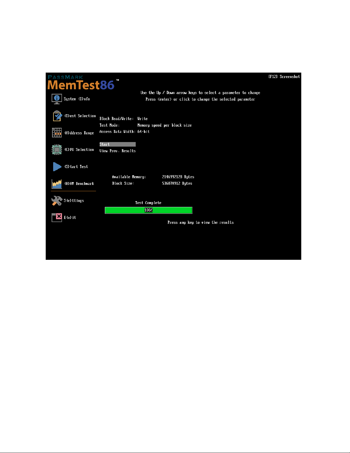
2.5.6.5 RAM Benchmark
The RAM Benchmark screen allows the user to benchmark their RAM modules, and save the results to disk. The
benchmark results can then be plotted onto a graph for comparison.
Block Read/Write - specifies whether memory read or write performance should be benchmarked
Test Mode - specifies which of the following tests to perform:
Memory Speed Per Access Step Size
This test measures the memory speed with respect to memory accesses of varying distances. This test
runs through a block of memory sequentially, accessing every address. Next, it runs through the same
block again, except this time it accesses every second address (step size 2). Then every fourth address
(step size 4) is accessed and so on, until a certain maximum step size is reached. We should expect to see
a decline in memory speed as the distance between memory accesses increase.
Memory Speed Per Block Size
This test measures the memory speed with respect to varying memory block sizes. On each subsequent
iteration, the block size is increased until a certain maximum block size is reached. Typically, a drop in
speed shall be observed when the block no longer fits in the respective cache levels, resulting in the
Page 27
Copyright 2024 PassMark® Software Page 27
much slower access to main memory.
Access Data Width – (Memory Speed Per Block Size only) The size of data in bits (8, 16, 32, or 64 bits) to access
at one time. The best results will usually be obtained when selecting an access size that matches the system's
native mode.
Start – performs the benchmark and saves the result to disk under Benchmark\. Pressing Esc will cancel the
test in the middle of testing.
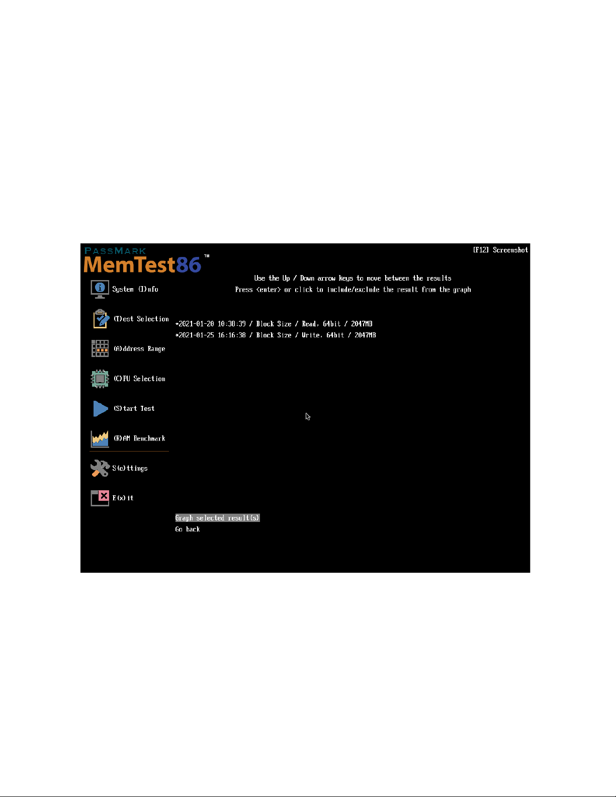
View Prev. Results – allows the user to select from a list of benchmark results saved under Benchmark\ to plot
on a graph
Use the up / down arrow keys or mouse to highlight a result to graph, then press enter or click. A maximum of 8
results can be plotted onto a single graph. Once all desired results are selected, selecting Graph selected
result(s) shall plot the selected result(s) to a graph.
Page 28
Copyright 2024 PassMark® Software Page 28
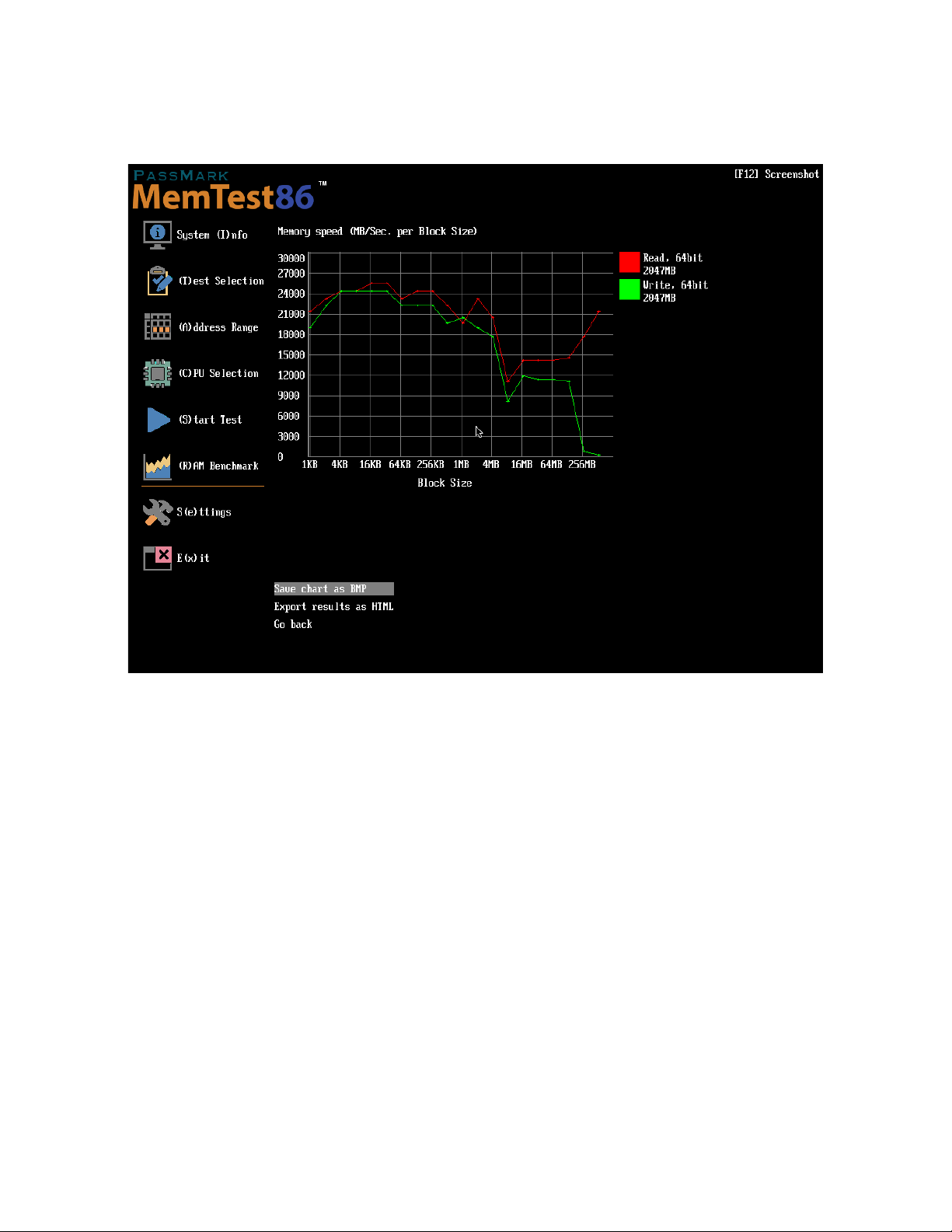
The graph can be saved to a bitmap file or exported into an HTML file as a report (Pro version only). The report
contains the system information, the graph itself, and the corresponding raw data.
Page 29

Copyright 2024 PassMark® Software Page 29
2.5.6.6 Settings
The Settings screen allows the user to set all other general configuration options pertaining to the MemTest86
tool.
Language - sets the language used in the program
Resolution - change the screen resolution (main menu only)
Save current configuration to file - (Pro version only) overwrites the mt86.cfg configuration file with the current
settings
Change log/report save location - (Pro version only) change the disk volume (file system) destination of log &
report files
Page 30

Copyright 2024 PassMark® Software Page 30
2.5.7 Configuration File (Pro version only)
Memory test parameters can also be set via a configuration file (mt86.cfg) that is loaded on startup, without
the need to manually configure the memory tests every time MemTest86 is run. This is useful especially in
testing environments where memory tests need to be executed in an automated fashion without user
intervention.
MemTest86 attempts to look for configuration files in the following order:
1. <SMBIOS-baseboard-product>-mt86.cfg
2. <Memory-size-in-GB>GB-mt86.cfg
3. mt86.cfg
MemTest86 shall first attempt to load a filename prefixed with the system’s baseboard (eg. Surface Pro-
mt86.cfg). This allows for separate configuration files for different baseboards, if running MemTest86 on
multiple systems.
If no suitable file was found, MemTest86 shall attempt to load a filename prefixed with the total memory size in
GB (eg. 8GB-mt86.cfg). This allows for separate configuration files depending on the size of memory.
Finally, if a suitable file is still not found, it will load the default mt86.cfg configuration file.
2.5.7.1 Basic Configuration File Format
The basic configuration file format supports a single configuration containing a set of parameter and value
pairs.
Lines that start with '#' indicate a comment line. All parameters are specified as follows:
[Parameter_name]=[Parameter_value]
A sample basic configuration file is as follows:
# MemTest86 basic configuration file
TSTLIST=0,1,3,5,8
TESTCFGFILE=customtests.cfg
NUMPASS=3
ADDRLIMLO=0x10000000
ADDRLIMHI=0x20000000
CPUSEL=PARALLEL
CPUNUM=1
CPULIST=2,3
MAXCPUS=32
ECCPOLL=0
ECCINJECT=0
MEMCACHE=0
LANG=ja-JP
AUTOMODE=1
EXITMODE=1
MINSPDS=0
EXACTSPDSIZE=8192
CHECKMEMSPDSIZE=1
SPDMANUF=Kingston
SPDPARTNO=9905402
SPDMATCH=1
HAMMERPAT=0x10101010
HAMMERMODE=SINGLE
Page 31

Copyright 2024 PassMark® Software Page 31
HAMMERSTEP=0x10000
MAXERRCOUNT=10000
2.5.7.2 Multiple Configuration File Format
The multiple configuration file format extends the basic format by supporting multiple configurations in a single
file.
Each set of configuration data would be separated via XML style tags as specified below:
<CONFIG=”Configuration-name-1”>
…
[Same as basic configuration format]
…
</CONFIG>
<CONFIG=”Configuration-name-2”>
…
[Same as basic configuration format]
…
</CONFIG>
….
Up to 10 <CONFIG> blocks are supported. Configuration name strings must be no more than 80 ASCII
characters and must not contain quotes (“) or angle bracket (< >) characters.
If more than one configuration is defined, the user shall be prompted during the MemTest86 boot phase as follows:
Multiple configurations detected. Please select one of the following:
1. Configuration-name-1
2. Configuration-name-2
The <CFGDEFAULT=X> tag is used to specify the default configuration. This can be either "LAST" or a number
between 1 and the number of configuration profiles. If “LAST” is specified, MemTest86 will attempt to read the
last configuration number from a file named [MAC-address].lastcfg (e.g. 00-50-56-3F-5C-05.lastcfg). If no such
file exists, configuration 1 (i.e. first configuration) will be used.
The <CFGTIMEOUT=X> tag is used to specify the timeout in seconds. Default is 0, which indicates no timeout.
If no configuration is selected after the timeout expires, the default configuration will be loaded.
A sample multiple configuration file is as follows:
# MemTest86 multiple configuration file
# Configuration 1
<CONFIG=”Short test, 1 pass, core tests only”>
TSTLIST=6,7,8
TESTCFGFILE=customtests.cfg
NUMPASS=1
MEMREMMB=16
MINMEMRANGEMB=16
</CONFIG>
# Configuration 2
<CONFIG=”Full test, 8 passes”>
TSTLIST=0,1,2,3,4,5,6,7,8,10,11,12
TESTCFGFILE=customtests.cfg
NUMPASS=8
MEMREMMB=16
Page 32

Copyright 2024 PassMark® Software Page 32
</CONFIG>
<CFGDEFAULT=LAST>
<CFGTIMEOUT=60>
During MemTest86 boot, the following prompt shall be displayed to the user:
Multiple configurations detected. Please select one of the following:
1. Short test, 1 pass, core tests only
2. Full test, 8 passes
Default configuration (*) shall be loaded in X seconds
2.5.7.3 List of Configuration Parameters
The following table summarizes the list of supported parameters:
Parameter
Description
TSTLIST
List of tests to execute in the test sequence. Each test is specified by a test number, separated
by a comma.
TESTCFGFILE
Specifies the name of the file containing custom individual test definitions. This replaces the
standard Test 0-13 individual tests used by default.
See
Custom test definitions (Pro version only) for file format specifications.
NUMPASS
Number of iterations of the test sequence to execute. This must be a number greater than 0.
ADDRLIMLO
The lower limit of the address range to test. To specify a hex address, the address must begin
with '0x'. Otherwise, the address shall be interpreted as a decimal address.
ADDRLIMHI
The upper limit of the address range to test. To specify a hex address, the address must begin
with '0x'. Otherwise, the address shall be interpreted as a decimal address.
MEMREMMB
Minimum amount of RAM (in MB) to leave unallocated for testing. This is to allow UEFI
runtime to operate properly without being memory starved. By default, this value is 16MB.
MINMEMRANGEMB
Minimum size (in MB) of contiguous memory ranges to allocate for testing. Memory ranges
smaller than this size should be left unallocated as it may be used by UEFI runtime. By
default, this value is 16MB.
CPUSEL
One of the following CPU selection modes:
'SINGLE', 'PARALLEL', 'RROBIN', 'SEQ'
CPUNUM
The CPU # of the logical CPU core to test in SINGLE CPU mode. This parameter only has an
effect if CPUSEL is set to 'SINGLE', and is ignored otherwise. This value must be less than the
value specified by MAXCPUS.
CPULIST
List of CPUs to enable for memory testing. This is useful for using only a subset of the
available CPUs when performing memory testing. Each CPU is specified by a CPU number,
separated by a comma. By default, all available CPUs are enabled.
MAXCPUS
The maximum number of logical CPUs cores to be enabled for testing. Only CPU numbers
less than this value can be enabled. By default, this value is 256. This value must be at least 1
and no more than 512.
DISABLEMP
Specifies whether to disable multiprocessor support. This can be used as a workaround for
certain UEFI firmwares that have issues running MemTest86 in multi-CPU modes.
Page 33

Copyright 2024 PassMark® Software Page 33
0 – Do not disable multiprocessor support (default)
1 – Disable multiprocessor support
ENABLEHT
Specifies whether to enable testing on hyperthreads. By default, memory tests are not run on
hyperthreads.
0 – Do not enable testing on hyperthreads (default)
1 – Enable testing on hyperthreads
ECCPOLL
Specifies whether ECC errors shall be polled.
0 – Polling disabled
1 – Polling enabled (default)
ECCINJECT
Specifies whether ECC error injection shall be enabled.
0 – ECC injection disabled (default)
1 – ECC injection enabled
MEMCACHE
Specifies whether memory caching shall be enabled/disabled during testing.
0 – Memory caching disabled
1 – Memory caching enabled (default)
PASS1FULL
Specifies whether the first pass shall run the full or reduced test. By default, the first pass
shall run a reduced test (ie. fewer iterations) in order to detect the most obvious errors as
soon as possible.
0 – Reduced test (default)
1 – Full test
ADDR2CHBITS
List of bit positions of a memory address to exclusive-or (XOR) to determine which memory
channel (A or B) is used. This is useful if you know that the memory controller maps a
particular address to a channel using this decoding scheme. If this parameter is specified and
MemTest86 detects a memory error, the channel number will be calculated and displayed
along with the faulting address. Each bit position specified is separated by a comma. For
example,
ADDR2CHBITS=1,8,9
will XOR bits 1,8,9 of the address to determine the channel.
ADDR2SLBITS
List of bit positions of a memory address to exclusive-or (XOR) to determine which slot (0 or
1) is used. This is useful if you know that the memory controller maps a particular address to
a slot using this decoding scheme. If this parameter is specified and MemTest86 detects a
memory error, the slot number will be calculated and displayed along with the faulting
address. Each bit position specified is separated by a comma. For example,
ADDR2SLBITS=3,4
will XOR bits 3,4 of the address to determine the slot.
ADDR2CSBITS
List of bit positions of a memory address to exclusive-or (XOR) to determine the chip select
bits (0 or 1). This is useful if you know that the memory controller maps a particular address
to a CS bit using this decoding scheme. If this parameter is specified and MemTest86 detects
a memory error, the CS bit will be calculated and displayed along with the faulting address.
Each bit position specified is separated by a comma. For example,
ADDR2CSBITS=5,11
will XOR bits 5, 11 of the address to determine the CS bit.
CHIPMAP[.{DDR4|DDR5}.{DIM
M|SODIMM}.{numranks}R.x{chip-
Lookup table used to map each DRAM chip to a unique ID label when tracking chip-level
errors (Site Edition only). The label string must be no more than 4 characters. By default, the
chips shall be labeled from U0...U15. For example,
Page 34

Copyright 2024 PassMark® Software Page 34
width}.{density}GB]
CHIPMAP= 00_A,01_A,02_A,03_A,00_B,01_B,02_B,03_B
shall label the first chip as “00_A”, the second chip as “01_A” and so forth according to the
ordering convention defined in DIMM / DRAM chip error decoding (Pro & Site Edition only)
There is a special case for labels that are non-negative numbers, where the string shall be
prepended with “U”. For example,
CHIPMAP=1,3,5,7,2,4,6,8
shall label the DRAM chips as “U1”, “U3”, “U5”, “U7”, “U2”, “U4”, “U6”, “U8”.
This parameter also supports different mappings for each RAM module configuration. This is
specified by optional attributes following the CHIPMAP parameter. For example,
# Map for all DDR5 modules
CHIPMAP.DDR5=3,4,5,6,7,8,9,10,11,12,13,14,15,16,17,18
# Map for all DDR5, SODIMM, 1-rank modules
CHIPMAP.DDR5.SODIMM.1R=1,2,3,4,11,12,13,14
# Map for all DDR5, DIMM, 1-rank, x8 width, 8GB modules
CHIPMAP.DDR5.DIMM.1R.x8.8GB=3,4,5,6,7,8,9,10
# Map for all DDR5, DIMM, 2-rank, x8 width, 16GB modules
CHIPMAP.DDR5.DIMM.2R.x8.16GB=3,4,5,6,7,8,9,10,11,12,13,14,15,16,17,18
# Map for all DDR4 modules
CHIPMAP.DDR4=1,2,3,4,6,7,8,9,10,11,12,13,14,15,16,17
# Map for all DDR4, SODIMM, 1-rank modules
CHIPMAP.DDR4.SODIMM.1R=1,2,3,4,11,12,13,14
# Map for all DDR4, DIMM, 1-rank, x8 width, 8GB modules
CHIPMAP.DDR4.DIMM.1R.x8.8GB=1,2,3,4,5,6,7,8
# Map for all DDR4, DIMM, 2-rank, x8 width, 16GB modules
CHIPMAP.DDR4.DIMM.2R.x8.16GB=1,2,3,4,6,7,8,9,10,11,12,13,14,15,16,17
If there are multiple matches, the chip map parameter that matches the most attributes shall
be applied.
LANG
Specifies one of the following languages to use:
'en-US' - English
'fr-FR' - French
'it-IT' - Italian
'es-AR' - Spanish (Latin American)
'pt-BR' - Portuguese (Brazil)
'de-DE' - German
'cs-CZ' - Czech
'pl-PL' - Polish
'ru-RU' - Russian
'ca-ES' - Catalan
'ja-JP' - Japanese
'zh-CN' - Chinese (Simplified)
'zh-HK' - Chinese (Traditional)
REPORTNUMERRS
Number of the most recent errors to display in the report file. This number must be no more
than 5000.
REPORTNUMWARN
Number of the most recent warnings to display in the report file. This number must be no
Page 35

Copyright 2024 PassMark® Software Page 35
more than 5000. Currently, this parameter is used only for the Hammer Test (Test 13)
REPORTPREFIX
Specifies whether the report filename shall be prepended with a prefix string.
'BASEBOARDSN' - Use the SMBIOS Baseboard serial number string
'SYSINFOSN' - Use the SMBIOS System Information serial number string
'DEFAULT' - None (Pro version); SMBIOS Baseboard serial number (Site edition)
AUTOMODE
Specifies the level of user intervention to use when running the memory tests.
0 – Auto mode disabled (default).
Splash screen and main menu are displayed. User is prompted to save the report file when
the tests have completed.
1 – Auto mode enabled.
The tests are started immediately, skipping the splash screen and main menu. Once the tests
have completed, the test results are automatically saved to the report file and the system is
rebooted.
2 – Auto mode w/ prompts.
The tests are started immediately, skipping the splash screen and main menu. Once the tests
have completed, the test results are automatically saved to the report file and waits for user
input before returning to the main menu.
AUTOREPORT
If AUTOMODE is set to 1 or 2, this parameter specifies whether to automatically save test
results to the report file.
0 – Do not save test results automatically
1 – Save test results automatically (default)
AUTOREPORTFMT
Specifies the format of the report when AUTOMODE is enabled and AUTOREPORT=1.
'HTML' - Save the report as an HTML file (default)
'BIN' - Save the report as a binary file, according to the following structure:
See Binary results file (Pro version only) for the binary file format.
AUTOPROMPTFAIL
Specifies whether to display the test result and ask for user intervention on test failure, even
when AUTOMODE is enabled
0 – Do not prompt for user intervention on test failure (default)
1 – Prompt for user intervention on test failure
SKIPSPLASH
Specifies whether to skip the 10 second splash screen and proceed directly to the main
menu.
0 – Do not skip splash screen (default)
1 – Skip splash screen and proceed directly to the main menu
SKIPDECODE
Specifies whether to skip the graphical DIMM decode results screen after test completion.
0 – Do not skip the DIMM decode screen
1 – Always skip the DIMM decode screen and proceed directly to the results summary
2 – Skip the DIMM decode screen for DDR4 systems
3 – Skip the DIMM decode screen for DDR5 systems
EXITMODE
Specifies the system behaviour when MemTest86 exits
0 – Reboot the system
1 – Shutdown the system
2 – Exit application and return control to UEFI BIOS
3 – Prompt the user (default)
MINSPDS
Minimum number of RAM SPDs to be detected before allowing the memory tests to begin.
EXACTSPDS
Exact number of RAM SPDs to be detected before allowing the memory tests to begin. If this
parameter is set, MINSPDS parameter is ignored.
EXACTSPDSIZE
Total size (in MB) of the capacity of all detected RAM SPDs to match before allowing the
memory tests to begin.
CHECKMEMSPDSIZE
Specifies whether to check if the total memory capacity of all RAM SPDs detected is
Page 36

Copyright 2024 PassMark® Software Page 36
consistent with the system memory size before allowing the memory tests to begin.
0 – Do not check for consistency (default)
1 – Check for consistency
SPDMANUF
Specifies a case-sensitive substring to match the JEDEC manufacturer of all detected RAM
SPDs before allowing the memory tests to begin.
SPDMATCH
Specifies whether to perform matching of RAM SPD bytes against the raw values stored in the
SPD.spd file before the tests start and after the tests complete. See
SPD.spd file specifications (Pro version only). The tests will not start if any of the
following are satisfied:
• There is a mismatch with the values stored in SPD.spd
• No valid SPD.spd file was found
• No SPD modules were detected
0 – Do not perform the SPD match check (default)
1 – Perform the SPD match check
SPDREPORTBYTELO
Specifies the lower offset of the SPD byte range to include in the HTML report. Must be less
than or equal to SPDREPORTBYTEHI.
SPDREPORTBYTEHI
Specifies the upper offset of the SPD byte range to include in the HTML report. Must be
greater or equal to SPDREPORTBYTELO.
SPDPARTNO
Specifies a case-sensitive substring to match the part number of all detected RAM SPDs
before allowing the memory tests to begin.
SAMESPDPARTNO
Specifies whether the RAM SPD Part Numbers must match before allowing the memory tests
to begin.
BGCOLOR
Specifies an alternative background colour to use:
'BLACK'
'BLUE'
'GREEN'
'CYAN'
'RED'
'MAGENTA'
'BROWN'
'LIGHTGRAY
HAMMERPAT
Specifies a 32-bit data pattern to use for the row hammer test (Test 13). If this parameter is
not specified, random data patterns are used.
HAMMERMODE
Specifies one of the following hammering algorithms to use for the row hammer test (Test
13):
'SINGLE' - single-sided hammer test
'DOUBLE' - double-sided hammer test (default)
HAMMERSTEP
The step size in bytes to use to determine the next row address pair to hammer. The size can
be specified as a decimal or hex number. To specify a hex number, the size must begin with
'0x'. This value must be greater than or equal to 64 bytes.
CONSOLEMODE
Specifies the console mode to use for the UEFI console. The UEFI firmware supports 1 or
more console modes that determines the resolution of the console. All UEFI firmware
supported mode 0 which is the minimum supported resolution of 80x25.
CONSOLEONLY
Specifies whether to run using the console only (ie. no graphics). This allows for systems
without graphics support (eg. Systems with serial console only)
0 – Normal mode (Enable graphics support)
Page 37

Copyright 2024 PassMark® Software Page 37
1 – Console only mode (Do not enable graphics support)
BITFADESECS
Specifies the sleep time in seconds to use for the Bit Fade test (Test 10). By default, the sleep
time is 300 seconds (5 minutes). This value must be between 180 seconds (3 minutes) and
600,000 seconds (166.67 hours).
In general, setting the sleep interval to a longer value shall test the data retention of RAM
more thoroughly. To our knowledge, although there have been no comprehensive studies
that determine the optimal sleep period, setting a sleep interval of 5 to 10 minutes would be
a good compromise between comprehensive testing and reasonable testing time.
MAXERRCOUNT
Specifies the maximum number of errors before the tests are aborted. By default, the value is
10000.
TFTPSERVERIP
Specifies a TFTP server IP address that is different from the PXE/DHCP server IP for saving the
report files
TFTPSTATUSSECS
Specifies the period in seconds to report the current test status to the TFTP server, which is
displayed in the management console. By default, the period is 60 seconds (1 minute). This
value must be between 10 seconds and 600 seconds (10 minutes).
TCPDISABLE
Specifies whether to disable attempts to connect via TCP/IP to the management console.
0 – Do not disable TCP/IP uploading to the management console (default)
1 – Disable TCP/IP connection to the management console
TCPSERVERIP
Specifies a TCP/IP server IP address for connection to the management console
TCPSERVERPORT
Specifies a TCP server port for connection to the management console
TCPCLIENTIP
Specifies a local TCP/IP address when DHCP is not enabled
DHCPDISABLE
Specifies whether to disable attempts to automatically configure a local IP address from a
DHCP server on the network. Memtest86 will default to using the address specified with the
TCPCLIENTIP address if DHCP is disabled.
0 – Do not disable automatic local IP address configuration
1 – Disable automatic local address configuration (default)
PMPDISABLE
Specifies whether to disable Management Console integration via TFTP uploading of XML
messages
0 – Do not disable TFTP uploading of XML messages (default)
1 – Disable TFTP uploading of XML messages
RTCSYNC
Specifies whether to set the real-time clock (RTC) by reading a file, CurrentText.txt, from the
PXE server. The format of the time is as follows:
YYYY-MM-DD hh:mm:ss
For example,
2020-05-22 00:53:14
0 – Do not synchronize the real-time clock with the PXE server (default)
1 – Synchronize the real-time clock with the PXE server
TRIGGERONERR
Specifies whether to enable triggering on memory error for use with logic analyzers. Before
the test is started, the memory address of the structure where errors are logged is displayed
on screen to allow for configuration of the logic analyzer. When memory errors are detected,
the pattern 0xDEADBEEF and error details are written to the following structure:
struct ERRINFO {
UINT64 Signature; // Stores 0xDEADBEEFDEADBEEF
UINT64 PhysAddr; // Stores the address of the error
__declspec(align(16)) __m128i Expected; // Expected pattern
Page 38

Copyright 2024 PassMark® Software Page 38
__declspec(align(16)) __m128i Actual; // Actual pattern
__declspec(align(16)) __m128i ErrorBits; // Bits in error
};
0 – Do not trigger and log on memory errors (default)
1 – Trigger and log memory errors to a specified location in memory
VERBOSITY
Specifies the verbosity level of the debug output
0 – Lowest verbosity level (default)
1 – Highest verbosity level
TPL
Specifies the UEFI task priority level of the MemTest86 application. UEFI tasks with higher
priority level may interrupt and preempt MemTest86.
'APPLICATION' - lowest priority level (default)
'CALLBACK' - intermediate priority level
'NOTIFY' - high priority level
'HIGH_LEVEL' - highest priority level
Some of the parameters (such as NUMPASS, ADDRLIMLO, ADDRLIMHI) can be changed via the main menu.
These changes are not automatically updated in the configuration file unless explicitly saved by the user. This
can be done under the ‘Settings’ screen in the main menu.
Page 39
Copyright 2024 PassMark® Software Page 39
2.5.8 Testing
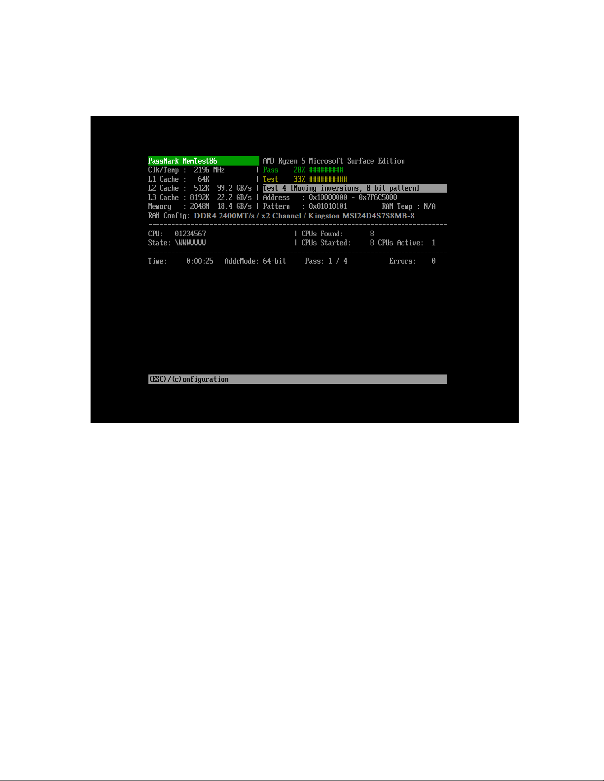
Once the memory test has started, the following screen which shows the test status is displayed:
MemTest86 executes a series of numbered test sections to check for errors. The execution order for these tests
has been arranged so that errors will be detected as rapidly as possible.
The time required for a complete pass of MemTest86 will vary greatly depending on CPU speed, memory speed
and memory size.
If memory errors are detected they will be displayed on the lower half of the screen.
If MemTest86 runs multiple passes without errors, it is very likely the memory is functioning properly. In
addition, successful execution of MemTest86 implicitly assures that your CPU (to a certain extent) is functioning
properly.
MemTest86 cannot diagnose many types of PC failures. For example, a faulty CPU that causes Windows to
crash will most likely cause MemTest86 to crash as well.
See Troubleshooting Memory Errors for details on how to interpret memory errors detected by MemTest86.
Page 40
Copyright 2024 PassMark® Software Page 40
2.5.8.1 Runtime Configuration Options
MemTest86 may be configured during operation via runtime configuration commands. Pressing the “C” key at
anytime will display the runtime command menu.
Settings:
(1) Skip Current Test
(2) End Test
(0) Continue
The runtime configuration commands allow the user to adjust the following settings.
(1) Skip Current Test- Aborts the current test and starts the next test in the sequence
(2) End Test - Stops the test and displays a summary of the results
(3) Continue - Resume the test
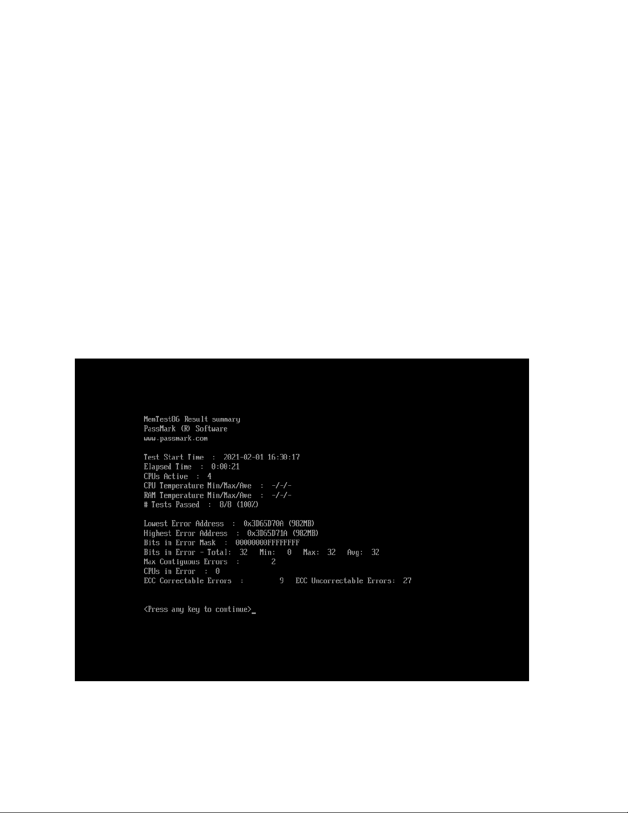
2.5.9 Test Results/Reports
At the end of the test, a summary of the test results is displayed, as shown in the following screenshot:
Page 41

Copyright 2024 PassMark® Software Page 41
Lowest Error Address:
The lowest address that where an error has been reported.
Highest Error Address:
The highest address that where an error has been reported.
Bits in Error Mask:
A mask of all bits that have been in error (hexadecimal).
Bits in Error:
Total bit in error for all error instances and the min, max and average bit in error of each individual occurrence.
Max Contiguous Errors:
The maximum of contiguous addresses with errors.
CPUs that detected memory errors:
List of CPU cores that detected memory errors.
ECC Correctable/Uncorrectable Errors:
The number of errors that have been corrected/uncorrected by ECC hardware.
Test Errors:
On the right hand side of the screen the number of errors for each test are displayed.
2.5.9.1 HTML Report file
To save the test results as an HTML report, press 'y' to save when prompted. Note the file name of the report as
this will be saved to the boot media (eg. USB or PXE) that MemTest86 booted from. This is shown in the
screenshot below.
For Pro and Site editions, HTML report files can be automatically saved by specifying the AUTOMODE and
AUTOREPORTFMT configuration file parameters. See Configuration File (Pro version only) for more details about
Page 42

Copyright 2024 PassMark® Software Page 42
configuration file parameters.
When network booting from PXE (Site edition only), HTML reports are uploaded to the PXE server. This can be
useful for automated workflows such as production line environments.
2.5.9.1.1 Blacklisting RAM Pages (Pro version only)
MemTest86 automatic generates Linux BadRAM and Windows badmemorylist string patterns from
detected errors in the HTML report, which can be passed to the operating system to allow the system to
temporarily boot. See Blacklisting RAM Pages for instructions on how to use RAM blacklist string patterns.
2.5.9.1.2 Customizing Test Reports (Pro version only)
The test report is fully customizable by modifying the following files:
mt86head.htm - The HTML code that will be used as a header for the test report. This can contain a company
logo, contact information or any additional information about the test environment.
mt86foot.htm – The HTML code that will be used as a footer for the test report. Examples of usage include a
signature line to indicate the technician who performed the test, or a disclaimer about the validity of the test
results.
report.css – The stylesheet used to specify the appearance of the report. The file itself contains all the
properties that are used, along with several templates that can be used to customize the report.
2.5.9.2 Binary results file (Pro version only)
For environments with limited storage space and processing capacity, the user may choose to save the results
as a binary file. The format of the binary file is as follows.
typedef struct _TESTRESULT {
CHAR8 Signature[4];// "MT86" signature
UINT16 Revision; // Current revision: 1.1 (Upper byte: major version; Lower byte: minor version)
UINT32 StartTime; //Start test time in Unix time, accurate to 1 sec
UINT32 ElapsedTime;//Test elapsed time in seconds
UINT64 RangeMin; //Min address tested
UINT64 RangeMax; //Max address tested
UINT16 CPUSelMode; //0-Single CPU, 1-Parallel, 2-Round Robin, 3-Sequential
INT16 CPUTempMin; //Min CPU temp for duration of test (-1 if N/A)
INT16 CPUTempMax; //Max CPU temp for duration of test (-1 if N/A)
INT16 CPUTempAve; //Ave CPU temp for duration of test (-1 if N/A)
INT16 RAMTempMin; //Min RAM temp for duration of test (-1 if N/A)
INT16 RAMTempMax; //Max RAM temp for duration of test (-1 if N/A)
INT16 RAMTempAve; //Ave RAM temp for duration of test (-1 if N/A)
BOOLEAN ECCSupport;//0 if ECC not supported, != 0 if ECC supported
INT8 TestResult; // {0:PASS, 1:INCOMPLETE PASS, -1:FAIL, -2:INCOMPLETE FAIL}
UINT32 ErrorCode; // Error code
UINT32 NumErrors; //Number of errors from all tests. Must be 0 if Passed == True
UINT64 MinErrorAddr;//Lowest address that had an error
UINT64 MaxErrorAddr;//Highest address that had an error
UINT64 ErrorBits; //Bit coded field showing the bits in error
UINT32 NumCorrECCErrors;//Number of detected and corrected ECC errors from all tests.
UINT32 NumUncorrECCErrors;//Number of detected but uncorrected ECC errors from all tests.
UINT8 Reserved[14]; // For future use
UINT16 NumTestsEnabled;// Number of individual tests enabled
Page 43

Copyright 2024 PassMark® Software Page 43
struct {
UINT8 TestNo; // Test ID number
UINT16 NumTestsPassed;// Number tests passed for this test number
UINT16 NumTestsCompleted;// Number tests completed for this test number
UINT32 NumErrors; // Number of errors detected for this test number
} AllTests[1]; // Variable-sized array of size=NumTestsEnabled
struct SLOTCHIP_ERRINFO {
UINT16 SlotChipErrsArrCount; // Size of variable-sized array SlotChipErrs below
struct {
INT8 Slot; // Slot number (-1 for unknown)
INT8 Chip; // Chip number (-1 for unknown)
UINT32 NumErrors; // Number of errors detected for this slot/chip combination
} SlotChipErrs[1];
} SlotChipErrInfo;
} TESTRESULT;
Binary result files cannot be saved manually and can only be saved by specifying the AUTOMODE and
AUTOREPORTFMT configuration file parameters. See Configuration File (Pro version only) for more details about
configuration file parameters.
As with HTML report files, binary results can be automatically saved to disk or uploaded to the PXE server,
supporting automated workflows such as production line environments.
2.5.10 DIMM / DRAM chip error decoding (Pro & Site Edition only)
MemTest86 V10 and later (Pro version) supports decoding and identification of the DIMM module on which a
particular error occurred. This can be used to narrow down potentially bad RAM modules more efficiently. This
is done by decoding the memory address with an error and locating the physical hardware that corresponds to
that address. RAM access involves multiple memory channels, multiple ranks, interleaving and hashing of
addresses making this a complex process.
Page 44

Copyright 2024 PassMark® Software Page 44
If supported, MemTest86 reports the decoded DIMM and DRAM chip when memory errors are detected during
testing. In addition, a graphical summary report of memory errors for each module is displayed on test
completion (shown below), as well as in the HTML report.
MemTest86 (Site Edition) further supports decoding of the individual DRAM chip in which the error occurred.
The DRAM chip mapping (eg. U0...U7) can be defined with the configuration file parameter CHIPMAP.
See Configuration File (Pro version only) for more details about configuration file parameters.
The chip ordering convention is illustrated in the images below.
Page 45

Copyright 2024 PassMark® Software Page 45
DDR5 UDIMM 1 Rank x8
DDR5 UDIMM 2 Rank x8
DDR5 SODIMM 1 Rank x8
DDR5 SODIMM 2 Rank x8
DDR5 UDIMM 1 Rank x16
DDR5 SODIMM 1 Rank x16
Page 46

Copyright 2024 PassMark® Software Page 46
Note that due to the nature of the tests, accurate slot and chip decoding is not possible for test 6 or test 14. As
such, no errors found during either test are decoded.
2.5.11 Troubleshooting MemTest86 Problems
A log file (MemTest86-<timestamp>.log) is automatically created and updated while MemTest86 is running. This
log file contains information that is helpful in diagnosing possible memory failures or problems with
MemTest86 itself. If you believe you may have encountered a bug with MemTest86, please report problems to
help@passmark.com.
Page 47

Copyright 2024 PassMark® Software Page 47
3 Troubleshooting Memory Errors
Please be aware that not all errors reported by MemTest86 are due to bad memory. The test implicitly tests the
CPU, L1 and L2 caches as well as the motherboard. It is impossible for the test to determine what causes the
failure to occur. However, most failures will be due to a problem with memory module. When it is not, the only
option is to replace parts until the failure is corrected.
Sometimes memory errors show up due to component incompatibility. A memory module may work fine in one
system and not in another. This is not uncommon and is a source of confusion. In these situations the
components are not necessarily bad but have marginal conditions that when combined with other components
will cause errors.
Often the memory works in a different system or the vendor insists that it is good. In these cases the memory is
not necessarily bad but is not able to operate reliably at full speed. Sometimes more conservative memory
timings on the motherboard will correct these errors. In other cases the only option is to replace the memory
with better quality, higher speed memory. Don't buy cheap memory and expect it to work reliably. On occasion
"block move" test errors will occur even with name brand memory and a quality motherboard. These errors are
legitimate and should be corrected.
All valid memory errors should be corrected. It is possible that a particular error will never show up in normal
operation. However, operating with marginal memory is risky and can result in data loss and even disk
corruption. Even if there is no overt indication of problems you cannot assume that your system is unaffected.
Sometimes intermittent errors can cause problems that do not show up for a long time. You can be sure that
Murphy will get you if you know about a memory error and ignore it.
We are often asked about the reliability of errors reported by MemTest86. In the vast majority of cases errors
reported by the test are valid. There are some systems that cause MemTest86 to be confused about the size of
memory and it will try to test non-existent memory. This will cause a large number of consecutive addresses to
be reported as bad and generally there will be many bits in error. If you have a relatively small number of failing
addresses and only one or two bits in error you can be certain that the errors are valid. Also intermittent errors
are without exception valid. Frequently memory vendors question if MemTest86 supports their particular
memory type or a chipset. MemTest86 is designed to work with all memory types and all chipsets.
MemTest86 cannot diagnose many types of PC failures. For example a faulty CPU that causes Windows to crash
will most likely just cause MemTest86 to crash in the same way.
3.1 Hammer Test (Test 13) Errors
The Hammer Test is designed to detect RAM modules that are susceptible to disturbance errors caused by
charge leakage. This phenomenon is characterized in the research paper Flipping Bits in Memory Without
Accessing Them: An Experimental Study of DRAM Disturbance Errors by Yoongu Kim et al. According to the
research, a significant number of RAM modules manufactured 2010 or newer are affected by this defect. In
simple terms, susceptible RAM modules can be subjected to disturbance errors when repeatedly accessing
addresses in the same memory bank but different rows in a short period of time. Errors occur when the
Page 48

Copyright 2024 PassMark® Software Page 48
repeated access causes charge loss in a memory cell, before the cell contents can be refreshed at the next
DRAM refresh interval.
Starting from MemTest86 v6.2, the user may see a warning indicating that the RAM may be vulnerable to high
frequency row hammer bit flips. This warning appears when errors are detected during the first pass (maximum
hammer rate) but no errors are detected during the second pass (lower hammer rate). See A.2 MemTest86 Test
Algorithms for a description of the two passes that are performed during the Hammer Test (Test 13). When
performing the second pass, address pairs are hammered only at the rate deemed as the maximum allowable
by memory vendors (200K accesses per 64ms). Once this rate is exceeded, the integrity of memory contents
may no longer be guaranteed. If errors are detected in both passes, errors are reported as normal.
The errors detected during Test 13, albeit exposed only in extreme memory access cases, are most certainly real
errors. During typical home PC usage (eg. web browsing, word processing, etc.), it is less likely that the memory
usage pattern will fall into the extreme case that make it vulnerable to disturbance errors. It may be of greater
concern if you were running highly sensitive equipment such as medical equipment, aircraft control systems, or
bank database servers. It is impossible to predict with any accuracy if these errors will occur in real life
applications. One would need to do a major scientific study of 1000 of computers and their usage patterns,
then do a forensic analysis of each application to study how it makes use of the RAM while it executes. To date,
we have only seen 1-bit errors as a result of running the Hammer Test.
There are several actions that can be taken when you discover that your RAM modules are vulnerable to
disturbance errors:
• Do nothing
• Replace the RAM modules
• Use RAM modules with error-checking capabilities (eg. ECC)
Depending on your willingness to live with the possibility of these errors manifesting itself as real problems, you
may choose to do nothing and accept the risk. For home use you may be willing to live with the errors. In our
experience, we have several machines that have been stable for home/office use despite experiencing errors in
the Hammer Test.
You may also choose to replace the RAM with m odules that have been known to pass the Hammer Test.
Choose RAM modules of different brand/model as it is likely that the RAM modules with the same model would
still fail the Hammer test.
For sensitive equipment requiring high availability/reliability, you would replace the RAM without question and
would probably switch to RAM with error correction such as ECC RAM. Even a 1-bit error can result in
catastrophic consequences for say, a bank account balance. Note that not all motherboards support ECC
memory, so consult the motherboard specifications before purchasing ECC RAM.
3.2 DMA Test (Test 14) Errors
The DMA test involves executing DMA-initiated memory transfers between the scratch partition of the
Page 49

Copyright 2024 PassMark® Software Page 49
MemTest86 USB flash drive and the system memory. As this introduces an additional component to the data
flow, errors detected by MemTest86 may not be an issue with the memory or DMA subsystem, but with the
USB flash drive itself.
If MemTest86 detects errors during the DMA Test, there is a possibility of a fault in the USB flash drive. In such
cases, it is recommended to re-run the tests using another known reliable USB flash drive.
If the errors persist, there may still be a possibility of a UEFI bug with the device driver DMA implementation.
This is usually indicated by a sudden increase in the number of errors. If you suspect this may be the case,
please see Troubleshooting MemTest86 Problems.
3.3 ECC Errors
During testing, MemTest86 may report ECC errors detected by the baseboard’s memory controller if ECC is
supported and enabled. The degree of information available for the detected ECC error depends on the
baseboard chipset. This includes any of the following:
• Memory address
• DRAM address (column, row, rank, bank)
• Channel and DIMM slot number
The following examples illustrate possible outputs displayed on screen for detected ECC errors .
[ECC Error] Test: 1, Addr: 0x8F32540AC
The ECC error was detected in memory address 0x8F32540AC.
[ECC Error] Test: 1, (Ch,Sl,Rk,Bk,Rw,Cl): (1,0,2,0,17900,0)
The ECC error was detected in the DIMM module located in channel 1, slot 0 with the indicated rank address
(0x2), and bank address (0x0), row address (0x17900), column address (0x0).
[ECC Error] Test: 1, Channel/Slot: 1/0
The ECC error was detected in the DIMM module located in channel 1, slot 0. No information regarding the
memory address that triggered the ECC error is available.
Page 50

Copyright 2024 PassMark® Software Page 50
4 Repairing Memory Faults
When MemTest86 detects errors the error count will be incremented and the error details will be displayed on
the lower half of the screen. The key information needed to diagnose errors are the “Error Confidence Value”
and the “Errors per Memory Slot” information. Error confidence values over 100 should always be considered
to be legitimate. The errors per memory slot indicate both the number of memory modules present in your PC
and the number of errors for each memory module. This information may not be available for older PCs. The
remaining error details may be ignored.
To diagnose and repair a memory fault requires you to open your computer case and handle sensitive
electronic components. With proper handling procedures this is not difficult. If you do not want repair your
own hardware you can use MemTest86 to test your RAM, but rely on a third party to do the actual repair.
4.1 Anti-Static Handling Procedures
Electronic components may be damaged by static electricity. The key to proper handling is to simply avoid
causing a static discharge though the component that is being handled. This is done by discharging static
buildup before a component comes in contact with another surface. For example when installing a component
into a computer, first touch a bare metal part of the computer case. If you want to set a component on a table,
touch the table first and then set down the component. If you take a step or even shuffle your feet you will
need to re-discharge any static buildup.
4.2 Re-Seating Memory Modules
In many cases memory problems are caused by a poor connection. This can be resolved by simply removing and
reinstalling the memory module(s) using the following procedure.
1. Using the documentation for your motherboard locate the memory module slots and identify the
memory module(s).
2. Using proper anti-static handing procedures remove the memory module(s). In most cases this is done
by pressing down on the locking tabs at the end of the module slot.
3. Carefully clean any dust or debris from the module and the motherboard memory module slots.
4. Reinstall the memory module(s) into their original slot on the motherboard.
5. Rerun MemTest86.
4.3 Replacing Modules
If re-seating memory modules does not resolve the problem then a memory module will generally need to be
replaced.
When more than one module is installed you will need to determine which module is failing.
First consult your motherboard documentation to determine if memory modules may be used individually or if
they must be used in pairs. If your motherboard is configured with the minimum number of memory modules
you will need to purchase a replacement memory module in order to locate the failing one. Using the
Page 51

Copyright 2024 PassMark® Software Page 51
guidelines in your motherboard manual to maintain a working configuration selectively remove modules from
the system and rerun MemTest86 to find the bad module(s). Be sure to carefully note which modules are in the
system when the test passes and fails.
In most cases memory failures will be due to a faulty memory module and replacing the module will resolve the
problem. However, the motherboard affects memory operation and may also cause memory errors. There are
instances where only a particular combination of memory and motherboard will cause errors. This is typically
due to the memory not being of sufficient quality and speed to keep up with the motherboard. This memory
may function properly when installed in a less demanding motherboard. When errors are only detected by test
#5 it is usually due to memory not being fast enough to work properly with the motherboard. More
conservative memory timing BIOS settings (if supported) may resolve these problems. Otherwise higher quality
memory may be required, or possibly the motherboard may need to be replaced.
4.4 Error Validity
There are many users who question if errors detected by MemTest86 are valid. In at least 99.9% of cases
reported errors will be legitimate and must be corrected. MemTest86 simply exercises all available RAM looking
for errors. If any error is detected in RAM, regardless of how or where, it is a legitimate failure that needs to be
corrected. There are no known issues regarding compatibility. It is possible, but unlikely, that a particular error
will never show up in normal operation. However, operating with marginal memory is risky and can result in
data loss and disk corruption. Even if there is no overt indication of problems you cannot assume that your
system will be unaffected.
There are some rare cases where motherboard manufacturers will map hardware registers into space normally
occupied by memory. When these locations are tested errors are reported. In this case, the reported errors will
be invalid. To better identify these rare cases where invalid errors are reported an error confidence value is
created by MemTest86. The program tracks failures and then does some simple analysis to determine the
probability of invalid errors. When the confidence value exceeds 100 it is nearly impossible that the reported
errors will be invalid.
Page 52

Copyright 2024 PassMark® Software Page 52
5 Over Clocking
5.1 Background
MemTest86 is an invaluable tool for over clocking and may be used to increase your systems performance and
reliability. Many shy away from over clocking fearing that it will make their PC less reliable. With a proper
procedure, fine tuning your system timings is safe and in some cases will even improve reliability.
Before embarking on over clocking one must understand the concept of margins or margin for error.
5.2 Operating Margins
To achieve high reliability computer systems are designed and tested under conditions that are more strenuous
than those expected in normal use. Take for example a computer that is designed to operate with a bus
frequency of 133 MHz. A quality manufacturer will design and test for operation at perhaps 140 MHz or higher.
This margin for error provides confidence that even with inevitable manufacturing variances and changing
conditions operation will be reliable. When components from different manufacturers are combined an even
greater margin for error is required since the exact characteristics of the associated components are not known.
The result is the majority of computers will end up having a much larger margin for error than is needed. This
means that a lot of performance is being wasted. On the other hand there will be a small number of systems
that do not have enough margin of error and will have poor reliability even without over clocking.
Many think of over clocking as simply making a computer operate as fast as possible. This approach is unwise
and will often result in unreliable operation. A much better philosophy is to adjust and fine tune computer
timings to maintain an appropriate margin for error. An appropriate margin includes not leaving too much
margin, wasting performance.
For example let say we have a computer that will operate properly with a system clock of 189 MHz. Obviously a
lot of performance will be wasted if we operate the computer at the standard 133 MHz. In addition if the
computer fails at 190 MHz it would be unwise to operate at 189 MHz since there is little margin for error and
operation will likely not be reliable. An operating margin of 3% to 6% is sufficient to insure good reliability. For
this example a system clock of 178 to 183 would be ideal. There may be cases where it will be advisable to
under clock. If a system with a normal clock rate of 133 MHz does not operate properly at 136 MHz or more
then there is not enough margin and under clocking is required to ensure reliability.
To summarize, over clocking should be thought of as fine tuning a computer to ensure reliability first and
secondarily maximizing performance.
5.3 Using MemTest86 for Over Clocking
The first step in a proper over clocking procedure is to determine the operational limits of your computer. After
the operational limits have been identified the system settings may be adjusted to provide enough margin to
ensure high reliability. MemTest86 is an ideal tool to accurately determine the operation limits of your memory
and CPU. Using the guidelines below, experiment with the settings available for your motherboard to find
settings that result in the highest clock rate combined with the highest reported memory bandwidth.
Page 53

Copyright 2024 PassMark® Software Page 53
1. Before attempting to over clock you need to know what system parameters your motherboard will
allow you to adjust and how they are adjusted. Some motherboards will allow all useful parameters to
be adjusted while others do not allow for any adjustment. Consult your motherboard manual for
details. Some of the parameters that may be available are:
• System clock rate
• CPU clock multiplier
• Memory timing
• Memory clock multiplier
• CPU voltage
• Memory voltage
2. You need to know how to reset the CMOS to factory settings. It is common when over clocking to end
up with settings that will not run the BIOS. When the parameters are set via CMOS the only way to
recover is to reset the CMOS to the factory configuration. For some motherboards this is accomplished
by removing a jumper. Other will require removal of the CMOS backup battery. Make sure that you
know how to recover before starting.
3. Before adjusting any parameters, run MemTest86 for a full pass to establish a baseline. Record the
memory bandwidth and CPU clock frequency for the default configuration.
4. Typically the best place to start is with the system clock rate. Increase the clock rate in fairly small
increments (2-4 MHz) and then run at least a partial pass of MemTest86. Running at least 15% of tests
1-5 should be the minimum amount of testing for each iteration. Continue increasing the clock rate
until you get a failure. Take your time and take good notes. For each step be sure that you record the
memory bandwidth reported by MemTest86. Some BIOS's automatically adjust memory timings
according to clock rate. You may find that by increasing the clock rate, memory performance will
decrease. Once you find a failure back off on the clock rate until you find the point at which you get
errors. Once you find the point at which memory errors occur back the clock off one step and run a full
pass of MemTest86 to confirm the operational limit. In some cases the CPU will hang (stop responding)
before memory errors are detected.
5. Some motherboards will allow you to adjust memory timing. Memory timings are typically listed as 4
values separated by hyphens. However, some motherboards only offer choices like fast, faster and
fastest. There are two strategies for adjusting memory timing. If memory errors are detected before the
CPU exhibits problems then slower memory timing may be used to allow a higher system clock rate to
be used. The second strategy is to use faster memory timings to get more memory bandwidth without
increasing the system clock rate. It is impossible to know which values will effect errors. Some of the
memory timings will affect memory bandwidth and others will not. Be sure to record the reported
memory bandwidth for each parameter change.
6. If in step 4 the CPU hangs before memory errors appear then the CPU has less margin for error than the
Page 54

Copyright 2024 PassMark® Software Page 54
memory. If available you may want to try reducing the CPU multiplier and then continue to increase the
system clock until either the CPU stops or memory errors occur. This is helpful if memory timings are
not adjustable or are ineffective.
7. CPU and memory voltages are adjustable on some motherboards and increasing them may allow you to
run at higher speeds. In particular higher CPU voltages tend to be quite effective for over clocking.
However, higher voltages also mean higher temperatures so be sure that you have plenty of case
cooling and an effective CPU cooler. Use carefully.
8. Some motherboards allow you to use a system clock multiplier for memory. The default is usually 1:1,
or in other words the system and memory clock rates will be the same. This setting is only useful when
the memory and CPU operational limits are significantly different and can not be brought into balance
using the techniques listed above.
Once you have established the operational limits of your system then you need to select settings that allow for
a reasonable margin for error. Do not be tempted to use the maximum settings! A margin of 3% to 6% is
recommended for reliable operation. The easiest way to add operational margin is to simply reduce the system
clock rate by 3% to 6% from the maximum setting that functioned properly.
In many cases the operational limits for the CPU and memory will be different. For example you can get more
CPU speed by reducing memory settings. Or you can get more memory performance by reducing the CPU
multiplier. For these cases you will need to choose a compromise. Both memory bandwidth and CPU clock rate
are important so don't be tempted to only optimize for one or the other.
MemTest86 provides good assurance of reliable memory operation when over clocking. Even when a dramatic
increase in memory bandwidth is achieved. As long as MemTest86 does not report errors and appropriate
margins have been applied then you should not hesitate to fully maximize memory timings. However, some
caution must be exercised for system clock rate increases. With most motherboards the clock rate for the PCI
and AGP busses are based on the system clock. Generally these busses will have no problem running at
somewhat higher rates. MemTest86 does not test PCI or AGP and do not provide any assurance that anything
other than the CPU and memory are working properly. Sadly there is currently no safe way to determine the
operational limits for PCI and AGP and therefor there is no way to assure that there are appropriate margins.
Unless your motherboard is able to independently establish the frequency of PCI and AGP busses you should be
careful about running with large (more than 15%) increases in the system clock. In addition running your CPU at
higher frequencies will generate more heat. Small frequency increases will generally be fine with the installed
CPU cooler. Larger increases in the system clock rate may necessitate a larger, more effective CPU cooler.
Page 55

Copyright 2024 PassMark® Software Page 55
Appendices
Appendix A. Technical Information
Appendix A contains technical information from the MemTest86 README file that was previously released
under the GNU Public License (GPL). This section provides additional background information and technical
information that may be useful for advanced users.
A.1 Memory Testing Philosophy
There are many approaches for testing memory. However, many tests simply throw some patterns at memory
without much thought or knowledge of memory architecture or how errors can best be detected. This works
fine for hard memory failures but does little to find intermittent errors. BIOS based memory tests are useless
for finding intermittent memory errors.
Memory chips consist of a large array of tightly packed memory cells, one for each bit of data. The vast
majority of the intermittent failures are a result of interaction between these memory cells. Often writing a
memory cell can cause one of the adjacent cells to be written with the same data. An effective memory test
attempts to test for this condition. Therefore, an ideal strategy for testing memory would be the following:
1. write a cell with a zero
2. write all of the adjacent cells with a one, one or more times
3. check that the first cell still has a zero
It should be obvious that this strategy requires an exact knowledge of how the memory cells are laid out on the
chip. In addition there is a never ending number of possible chip layouts for different chip types and
manufacturers making this strategy impractical. However, there are testing algorithms that can approximate
this ideal strategy.
Page 56

Copyright 2024 PassMark® Software Page 56
A.2 MemTest86 Test Algorithms
MemTest86 uses two algorithms that provide a reasonable approximation of the ideal test strategy above. The
first of these strategies is called moving inversions. The moving inversion test works as follows:
1. Fill memory with a pattern
2. Starting at the lowest address
2a. Check that the pattern has not changed
2b. Write the patterns complement
2c. Increment the address
Repeat 2a - 2c
3. Starting at the highest address
3a. Check that the pattern has not changed
3b. Write the patterns complement
3c. Decrement the address
Repeat 3a - 3c
This algorithm is a good approximation of an ideal memory test but there are some limitations. Most high
density chips today store data 4 to 16 bits wide. With chips that are more than one bit wide it is impossible to
selectively read or write just one bit. This means that we cannot guarantee that all adjacent cells have been
tested for interaction. In this case the best we can do is to use some patterns to insure that all adjacent cells
have at least been written with all possible one and zero combinations.
It can also be seen that caching, buffering and out of order execution will interfere with the moving inversions
algorithm and make less effective. It is possible to turn off cache but the memory buffering in new high
performance chips can not be disabled. To address this limitation a new algorithm called Modulo-X was
created. This algorithm is not affected by cache or buffering. The algorithm works as follows:
1. For starting offsets of 0 - 20 do steps 2-5
2. Write every 20th location with a pattern
3. Write all other locations with the patterns complement
4. Repeat 1b one or more times
5. Check every 20th location for the pattern
This algorithm accomplishes nearly the same level of adjacency testing as moving inversions but is not affected
by caching or buffering. Since separate write passes (1a, 1b) and the read pass (1c) are done for all of memory
we can be assured that all of the buffers and cache have been flushed between passes. The selection of 20 as
the stride size was somewhat arbitrary. Larger strides may be more effective but would take longer to execute.
The choice of 20 seemed to be a reasonable compromise between speed and thoroughness.
Page 57

Copyright 2024 PassMark® Software Page 57
A.2.1 Individual Test Descriptions
MemTest86 executes a series of numbered test sections to check for errors. These test sections consist of a
combination of test algorithm, data pattern and caching. The execution order for these tests were arranged so
that errors will be detected as rapidly as possible. A description of each of the test sections follows:
Address test, walking ones
Tests all address bits in all memory banks by using a walking ones address pattern. Errors from this test are not
used to calculate BadRAM patterns.
Address test, own address
Each address is written with its own address and then is checked for consistency. In theory previous tests
should have caught any memory addressing problems. This test should catch any addressing errors that
somehow were not previously detected.
Moving inversions, ones & zeros
This test uses the moving inversions algorithm with patterns of all ones and zeros. Cache is enabled even
though it interferes to some degree with the test algorithm. With cache enabled this test does not take long
and should quickly find all "hard" errors and some more subtle errors.
Moving inversions, 8 bit pattern
This is the same as test 3 but uses a 8 bit wide pattern of "walking" ones and zeros. This test will better detect
subtle errors in "wide" memory chips. A total of 20 data patterns are used.
Moving inversions, random pattern
This test uses the same algorithm as test 3 but the data pattern is a random number and it's complement. This
test is particularly effective in finding difficult to detect data sensitive errors. A total of 60 patterns are used.
The random number sequence is different with each pass so multiple passes increase effectiveness.
Block move
This test stresses memory by using block move (movsl) instructions and is based on Robert Redelmeier's
burnBX test. Memory is initialized with shifting patterns that are inverted every 8 bytes. Then 4MB blocks of
memory are moved around using the movsl instruction. After the moves are completed the data patterns are
checked. Because the data is checked only after the memory moves are completed it is not possible to know
where the error occurred. The addresses reported are only for where the bad pattern was found. Since the
moves are constrained to an 8MB segment of memory the failing address will always be lest than 8MB away
from the reported address. Errors from this test are not used to calculate BadRAM patterns.
Moving inversions, 32 bit pattern
This is a variation of the moving inversions algorithm that shifts the data pattern left one bit for each successive
address. The starting bit position is shifted left for each pass. To use all possible data patterns 32 passes are
Page 58

Copyright 2024 PassMark® Software Page 58
required. This test is quite effective at detecting data sensitive errors but the execution time is long.
Random number sequence
This test writes a series of random numbers into memory. The initial pattern is checked and then
complemented and checked again on the next iteration. However, unlike the moving inversions test, writing and
checking can only be done in the forward direction. On the first pass, a fixed seed number is used so that the
random number generator always generates the same sequence of numbers, allowing the test run to be
reproducible. All subsequent passes use a seed number generated from the system clock, resulting in more
permutations being tested.
The 64-bit and 128-bit versions of this test is essentially the same as the original 32-bit test, except that it uses
native 64-bit and SIMD instructions respectively.
Modulo 20, random pattern
Using the Modulo-X algorithm should uncover errors that are not detected by moving inversions due to cache
and buffering interference with the algorithm. A sequence of 6 32 bit random patterns are used.
Bit fade test, 2 patterns
The bit fade test initializes all of memory with a pattern and then sleeps for 5 minutes (or a custom userspecified time interval). Then memory is examined to see if any memory bits have changed. All ones and all
zero patterns are used.
Row Hammer Test
The row hammer test exposes a fundamental defect with RAM modules 2010 or later. This defect can lead to
disturbance errors when repeatedly accessing addresses in the same memory bank but different rows in a short
period of time. The repeated opening/closing of rows causes charge leakage in adjacent rows, potentially
causing bits to flip.
This test 'hammers' rows by alternatively reading two addresses in a repeated fashion, then verifying the
contents of other addresses for disturbance errors. For more details on DRAM disturbance errors, see Flipping
Bits in Memory Without Accessing Them: An Experimental Study of DRAM Disturbance Errors by Yoongu Kim et
al.
Starting from MemTest86 v6.2, potentially two passes of row hammer testing are performed. On the first pass,
address pairs are hammered at the highest possible rate. If errors are detected on the first pass, errors are not
immediately reported and a second pass is started. In this pass, address pairs are hammered at a lower rate
deemed as the worst case scenario by memory vendors (200K accesses per 64ms). If errors are also detected in
this pass, the errors are reported to the user as normal. However, if only the first pass produces an error, a
warning message is instead displayed to the user.
DMA Test
The DMA test exercises the DMA subsystem to initiate memory transfers without CPU intervention. This test is
Page 59

Copyright 2024 PassMark® Software Page 59
designed to detect memory errors that are exposed during DMA-based memory accesses initiated by
peripherals such as mass storage devices (eg. hard drives).
This test first initializes the contents in a scratch partition in the MemTest86 USB flash drive by performing a
DMA-based transfer from memory to disk. Once initialized, the data is verified by performing multiple iterations
of DMA-based transfer from disk back to memory. An error is detected If there are any data mismatches
between what was written and read from disk.
Page 60

Copyright 2024 PassMark® Software Page 60
A.3 Error Reporting
A.3.1 Memory Errors
When the tests are running, individual errors are reported which includes the following details.
Field
Description
Test:
Test number
Addr:
Failing memory address
Expected:
Expected data pattern
Actual:
Failing data pattern
A.3.2 ECC Errors
When ECC detection is enabled, the following error details are reported when ECC errors are detected. Some
fields may not be available depending on the memory controller on the chipset.
Field
Description
Test:
Test number
Addr:
Memory address of the detected ECC error
(Col,Row,Rank,Bank):
The rank, bank, row, and column address of the detected ECC error.
ECC Corrected:
Whether the ECC error has been corrected or not
Syn:
Represents the "ECC syndrome" value. When a 64-bit word is written to RAM, seven ECC bits
are computed. When the same word is re-read the ECC bits are recalculated. Then an
exclusive OR is done on the ECC bits to determine if there has been an error. A zero result
means no error. A non zero result indicates an error and the syndrome value can be used to
determine the actual bit that was in error. Consult the memory controller’s chipset
documentation for the ECC syndrome table to determine the exact bit in error.
Channel/Slot:
The channel and slot number of the DIMM stick where the ECC error was detected
Page 61

Copyright 2024 PassMark® Software Page 61
A.4 SPD.spd file specifications (Pro version only)
The SPD.spd file contains the raw bytes to be compared with the collected SPD data when the configuration file
parameter SPDMATCH=1. The format specifications is as follows:
• ASCII text format
• Maximum 512 bytes
◦ If the number of bytes is less than the size of the SPD data, only those bytes shall be compared with
the SPD data.
◦ If the number is greater, the check shall fail
• Only hex and '?' wildcard characters allowed, in pairs to represent a single byte
◦ If '?' is specified for a nibble, it will match any value for the corresponding nibble in the SPD data
Example
Given the following truncated SPD.spd file:
23 10 0C ?? AA BB CC DD EE FF 11 22 33 44 55 66
...
...
The following SPD bytes shall match:
23 10 0C 00 AA BB CC DD EE FF 11 22 33 44 55 66
...
...
However, the following SPD bytes shall not match:
23 10 0C 00 AB BB CC DD EE FF 11 22 33 44 55 66
...
...
Page 62

Copyright 2024 PassMark® Software Page 62
A.5 Custom test definitions (Pro version only)
By default, the list of tests described in Individual Test Descriptions compose the test suite to be executed for
any given test session. The execution order, test patterns and number of iterations for these tests were
designed to detect the most obvious errors quickly.
However, there may be non-standard test scenarios that require running an existing test algorithm with a
specific test pattern, cache configuration, and/or number of iterations. MemTest86 supports custom
configuration of existing test algorithms to support such test scenarios.
Note: Overriding the default tests is not recommended for novice users as it may reduce the test coverage and
erroneously produce a PASS result for faulty RAM modules. Override default tests at your own risk.
To enable custom test definitions, the TESTCFGFILE=<test-config-filename> configuration file parameter is set
to the name of the custom test definitions file. The custom test definitions file defines a list of comma-separated
values formatted as follows:
# Format:
# <test_type>, <pattern>, <iter_count>, <cache_enable>, <test_name>
#
# <test_type> can be one of :
# ADDRWALK1 - Address Test, Walking ones
# ADDROWN - Address Test, Own address
# MOVINV8 - Moving inversions, 8-bit
# BLKMOV - Block move
# MOVINV32 - Moving inversions, 32-bit
# RNDNUM32 - Random Number, 32-bit
# MOD20 - Modulo 20
# BITFADE - Bit fade test
# RNDNUM64 - Random number, 64-bit
# RNDNUM128 - Random number, 128-bit
# HAMMER - Hammer test
#
# <pattern> can be a hex value or:
# PAT_RAND - random pattern
# PAT_WALK01 - walking 0/1 patterns
# PAT_DEF - default pattern for the specified test type
#
# <iter_count> can be any positive integer or:
# ITER_DEF - test default
#
# <cache_enable> can be one of:
# CACHE_EN – cache enabled
# CACHE_DIS – cache disabled
# CACHE_DEF – global default cache settings
#
# <test_name> is a string describing the test
Page 63

Copyright 2024 PassMark® Software Page 63
An example custom test definitions file, customtests.cfg, is as follows. To enable the custom tests,
TESTCFGFILE=customtests.cfg must be specified in the mt86.cfg file
ADDRWALK1, PAT_DEF, ITER_DEF, CACHE_DIS, "Address test, walking ones, cache off"
MOD20, PAT_WALK01, 1, CACHE_EN, "Modulo 20, walking 0/1, cache on"
MOVINV32, PAT_DEF, ITER_DEF, CACHE_EN, "Moving invs 32b, rand pattern, cache on"
MOVINV8, 0x55555555, ITER_DEF, CACHE_DIS, "Moving invs 8b, 0x55555555, cache off"
Page 64

Copyright 2024 PassMark® Software Page 64
A.6 Blacklisting RAM Pages
Several operating systems allow the user to pass in a blacklist of 'bad' memory ranges to block the operating
system from using or allocating memory in that range. This is useful for cases where the RAM in the system fails
predictably on the same set of memory addresses. By masking known faulty addresses, the system may
temporarily be able to boot into the operating system to perform backup and additional diagnostics, where it
would otherwise crash during the boot process.
Note that masking faulty memory addresses does not fix defective RAM, but provides a temporary workaround
for allowing the system to boot, especially in the case of soldered memory that cannot be easily replaced. Faulty
memory should always be replaced, if possible.
A.6.1 Linux BadRAM
Most newer Linux kernels (eg. Ubuntu 12.04 or newer) support BadRAM, which allow a blacklist of memory
address & mask patterns to be passed in as a GRUB2 boot-time parameter. This work-around makes it possible
for Linux to reliably run with defective RAM. For history and background information on the original BadRAM
project by Rick van Rein, see the following page: http://rick.vanrein.org/linux/badram/
A.6.1.1 How to blacklist RAM regions
MemTest86 Pro (v9 or later) supports automatic generation of BadRAM string patterns from detected errors in
the HTML report, that can be used directly in the GRUB2 configuration without needing to manually calculate
address/mask values by hand.
To enter the address ranges to blacklist manually, do the following:
1. Edit /etc/default/grub and add the following line:
GRUB_BADRAM=addr,mask[,addr,mask...]
where the list of addr,mask pairs specify the memory range to block using address bit matching
Eg. GRUB_BADRAM=0x7ddf0000,0xffffc000 shall exclude the memory range 0x7DDF0000-0x7DDF4000
2. Open and terminal and run the following command
sudo update-grub
3. Reboot the system
A.6.1.2 How to view blacklisted RAM regions
To view the memory regions that have been blacklisted, do the following:
1. Open and terminal and run the following command
sudo cat /proc/iomem
...
7ddf0000-7ddf3fff : RAM buffer
...
Page 65

Copyright 2024 PassMark® Software Page 65
Memory ranges blacklisted by BadRAM are marked as RAM buffer
A.6.2 Windows badmemorylist
For Windows Vista and later, the blacklist of known 'bad' memory ranges can be passed in via the Boot
Configuration Data (BCD) system store. This is part of the Windows Hardware Error Architecture (WHEA) which
performs Predictive Failure Analysis (PFA) for ECC memory. For details of this feature, see the following page:
https://docs.microsoft.com/en-us/windows-hardware/drivers/whea/persistence-of-pfa-results
Note: Since Windows 10 2004, the blacklisted memory pages may no longer be recognized due to a possible
bug. This is described in this post here:
https://answers.microsoft.com/en-us/windows/forum/all/starting-with-windows-10-2004-the-pfa-memorylist/4148df72-851d-4618-8181-d785d802c8c7
A.6.2.1 How to blacklist RAM pages
MemTest86 Pro (v9 or later) supports automatic generation of badmemorylist command strings from
detected errors in the HTML report, that can pasted directly in the Command Prompt without needing to
manually calculate page numbers by hand.
To enter the page numbers to blacklist manually, do the following:
1. Open the Command Prompt (as Administrator) either from Windows or System Recovery options
2. Run the following command to enable memory blacklisting:
bcdedit /set {badmemory} badmemoryaccess no
3. Run the following command to blacklist the faulty page frame numbers (PFN):
bcdedit /set {badmemory} badmemorylist PFN1 [PFN2 PFN3 ...]
where the list of PFN values specify individual page numbers to block
Eg. bcdedit /set {badmemory} badmemorylist 0xA1 0xB8 0xB9 shall exclude the memory ranges
0xA1000-0xA1FFF, 0xB8000-0xB9FFF
Note: Windows Memory Diagnostics can also overwrite or delete the entire PFN list without notifying
the user. And at least in some cases Windows Memory Diagnostics might run as a background
scheduled task in Windows.
A.6.2.2 How to view blacklisted RAM pages
To view the list of page numbers that have been blacklisted, do the following:
1. Open the Command Prompt (as Administrator) either from Windows or System Recovery options
2. Run the following command to display the list of blacklisted pages:
bcdedit /enum {badmemory}
3. Alternatively, you may use the RAMMap tool from Microsoft.
Page 66

Copyright 2024 PassMark® Software Page 66
A.6.2.3 How to clear blacklisted RAM pages
To clear the list of page numbers that have been blacklisted, do the following:
1. Open the Command Prompt (as Administrator) either from Windows or System Recovery options
2. Run the following command to clear the list of blacklisted pages:
bcdedit /deletevalue {badmemory} badmemorylist
Page 67

Copyright 2024 PassMark® Software Page 67
Appendix B. Product Support
Please report problems to:
Email: help@passmark.com
Please include:
• The software version.
• A detailed description of the problem and how to reproduce it.
• A copy of the result files / log files (if available).
• Details of how we may be able to contact you.
B.1 Known Problems
MemTest86 can not diagnose many types of PC failures. For example a faulty CPU that causes Windows to
crash will most likely just cause MemTest86 to crash in the same way.
With some PC's MemTest86 will just die with no hints as to what went wrong. Without any details it is
impossible to fix these failures. Fixing these problems will require debugging on your part. There is no point in
reporting these failures unless you have a Linux system and would be willing to debug the failure.
MemTest86 supports all types of memory. If fact the test has absolutely no knowledge of the memory type nor
does it need to. This not a problem or bug but is listed here due to the many questions about this issue.
B.1.1 UEFI
MemTest86 depends on the services provided by the UEFI firmware, which include mouse/keyboard support,
multiprocessor services, file input/output, and PCI device management. Because the services that are provided
by the firmware are developed individually by the motherboard manufacturers, there may be functional
differences that can limit or prevent the proper operation of MemTest86. Some of these issues are highlighted
below:
• Some UEFI implementations do not provide full mouse support, preventing the use of the mouse in
MemTest86. If this is the case, use the keyboard or try updating to a new firmware build.
• Multiple CPU testing may not be available due to limited or non-functional multiprocessor services
provided by UEFI, especially for older firmware. This may cause a reduced number of processors
available for testing, or even program freeze when attempting to run on other processors. If this is the
case, run in single CPU mode or try updating to a new firmware build. There is a blacklist.cfg file that
contains a list of baseboards that are known to have issues running MemTest86. Adding a baseboard to
the list may allow MemTest86 to run, albeit with limited functionality. See Baseboard Blacklist File
(blacklist.cfg) for details on how to use the file.
MemTest86 is also inherently limited by the UEFI environment and as such, gives rise to the following
limitations:
• MemTest86 USB flash drives cannot be read in Windows XP (32-bit) due to its lack of support of GPT
Page 68

Copyright 2024 PassMark® Software Page 68
disks
• MemTest86 cannot remap itself to different portions of memory in order to run tests in the section of
memory it was occupying.
• Dual UEFI entries may be present in UEFI BIOS as boot devices. There is no difference in selecting either
entry This is due to a workaround that allows MemTest86 USB flash drives to be accessible in Windows.
B.1.1.1 Baseboard Blacklist File (blacklist.cfg)
There is a file (blacklist.cfg) that contains a list of baseboards that are known to have firmware issues that
prevent MemTest86 from functioning properly. This file is loaded on startup and the list is scanned to see if
there is a match with the system baseboard. If there is a match, the MemTest86 functionality shall be restricted
accordingly. Without imposing the restriction, there may be a chance that MemTest86 may not run at all. The
following is a snip-bit of the blacklist.cfg file:
"Mac-F42C88C8",ALL,EXACT,RESTRICT_STARTUP
"80AF",ALL,EXACT,RESTRICT_MP
"Z97MX-Gaming 5",ALL,EXACT,RESTRICT_MP
"Z170MX-Gaming 5",ALL,EXACT,RESTRICT_MP
Each blacklisted baseboard is stored on a separate line with the following format:
<baseboard>,<BIOS version>,<exact|partial match>,<restriction flags>
• <baseboard> is the case-sensitive baseboard string in double quotes
• <BIOS version> is the first BIOS version (string in double quotes) that no longer exhibits the issue. If
no fix is available, specify ALL
• <exact|partial match> determines whether exact or partial matching is used on <baseboard string>.
• <restriction flags> determines the restriction policy to impose if there is a match. This can be one
of the following values:
• RESTRICT_STARTUP - Display a warning message before MemTest86 boots
• RESTRICT_MP - Do not perform the multiprocessor test during startup, and set the default CPU mode to
SINGLE
• DISABLE_MP - Completely disable multiprocessor support, restricting the CPU mode to SINGLE only
• DISABLE_CONCTRL - Disable console control protocol, which may be needed for some older systems (eg.
iMac 7.1)
• FIXED_SCREENRES - Do not modify the default screen resolution, which is known to cause issues on some
Lenovo systems
• RESTRICT_ADDR - Set the lower address limit to 0x100000 by default, which may be needed for some Mac
systems (eg. Late 2013 27" iMac)
• TEST12_SINGLECPU - Run Test 12 in SINGLE CPU Mode, which may be necessary to workaround CPU
threads hanging in PARALLEL mode
• DISABLE_LANG - Disable language support and font installation, which is known to cause issues on some
Dell systems
Page 69

Copyright 2024 PassMark® Software Page 69
B.2 Enhancements
Please send enhancement requests to:
info@passmark.com
All requests will be considered, but not all can be implemented
Page 70

Copyright 2024 PassMark® Software Page 70
Appendix C. Change Log
Changes in v10.7 (Build 1000) (Feb/2024)
Fixes/Enhancements
• Preliminary support for obtaining memory settings for Intel Core chipsets:
o 2nd gen (Sandy Bridge)
o 3rd gen (Ivy Bridge)
o 4th gen (Haswell)
o 5th gen (Broadwell)
o 6th gen (Skylake)
o 7th gen (Kaby lake)
o 8th gen (Coffee Lake)
o 9th gen (Coffee Lake Refresh)
o 10th gen (Comet Lake/Ice Lake)
o 11th gen (Rocket Lake/Tiger Lake)
o 12th gen (Alder Lake)
o 13th gen (Raptor Lake) Core chipsets
• Preliminary support for obtaining memory settings for Intel Core Ultra chipsets:
o 1st gen (Meteor Lake)
o 2nd gen (Arrow Lake)
o Lunar Lake
• Preliminary support for obtaining memory settings for Intel Xeon scalable chipsets:
o 1st gen (Skylake-SP)
o 2nd gen (Cascade Lake-SP)
o 3rd gen (Ice Lake-SP)
o 4th gen (Sapphire Rapids-SP)
o 5th gen (Emerald Rapids-SP)
• Preliminary support for obtaining memory settings for Intel Atom X Series (Elkhart Lake) chipsets
• Preliminary ECC support for the following Intel chipsets:
o 10th gen core (Ice Lake)
o 1st gen core ultra (Meteor Lake)
o 5th gen Xeon scalable (Emerald Rapid)
o Atom X Series (Elkhart Lake)
• Preliminary support for module decoding for Intel 10th gen core (Ice Lake) chipsets
• Added support for reporting various ECC error types (eg. IBECC/Scrub)
• Fixed rounding of DDR5 latency timings
• Fixed offsetted temperatures for AMD 19h family chipsets
• Suppress CPU errors due to UEFI firmware issues once already displayed
• Display "SPD FAIL" block error message when SPDMATCH check fails after test completion
Page 71

Copyright 2024 PassMark® Software Page 71
• Updated localization strings (courtesy of Nagisa)
• Updated ImageUSB to v1.5.1006
• Updated blacklist
Changes in v10.6 (Build 3000) (Oct/2023)
New Features
• Added support for CFGDEFAULT tag for multi-config files to specify the default configuration
• Added support for CFGTIMEOUT tag for multi-config files to specify the timeout in seconds
Fixes/Enhancements
• Fixed possible divide by zero error when displaying file system info of attached disks
• Fixed system address to UMC decoding for AMD Ryzen chipsets
• Fixed incorrect transfer speed obtained for Alder Lake/Raptor Lake chipsets
Changes in v10.6 (Build 2000) (Aug/2023)
New Features
• Extend CHIPMAP configuration parameter to support arbitrary strings up to 4 characters. For backwards
compatibility, chip names that are non-negative numbers shall be prepended with "U".
Fixes/Enhancements
• Fixed CPU clock "MHz" cutoff in test screen
• Fixed report summary screen displaying invalid elapsed time and CPU temperatures
• Fixed text cutoff due to long strings for certain languages
• Fixed DIMM temperature text cutoff in test screen for certain languages
Changes in v10.6 (Build 1000) (Aug/2023)
New Features
• Added 'SPDREPORTBYELO' and 'SPDREPORTBYTEHI' configuration parameter for specifying the SPD byte
range to display in the HTML report
• Implemented workaround for reading DDR5 SPD when SPD write disable (SPDWR) is set for Intel
chipsets
• Added DIMM/IC decoding support for AMD Phoenix (19h 74h) chipsets
Fixes/Enhancements
• Added support for chipsets with up to 12 memory controllers
• Fixed hang due to reading non-existent MSR registers for AMD 19h 60-6fh chipsets
• Fixed channel decoding for AMD Ryzen Zen 2/4 chipsets
Page 72

Copyright 2024 PassMark® Software Page 72
• Fixed incorrect memory clock reported for Intel Alder Lake/Rocket Lake chipsets
• Fixed incorrect memory clock reported for AMD 19h 60-6fh chipsets
• Fixed incorrect CPU temperature reported for EPYC 7003 series chipsets due to temperature offsets
• Fixed DIMM temperature read failure after reading SPD for certain DDR5 modules
• Added reporting of additional DDR5 SPD attributes
• Fixed hang due memory allocation issues for Intel Skylake/Kaby Lake chipsets
• Added ECC support for additional Intel Skylake-SP chipset variants
• Added workaround for hang when obtaining list of benchmark results
• Perform cache invalidation before start of the RAM benchmark test to fix result inconsistencies
• Fixed text being unaligned when containing full-width characters
• Updated localization strings
• Updated blacklist
Changes in v10.5 (Build 1000) (Jun/2023)
New Features
• Added support for displaying and reporting configured RAM settings for supported chipsets. This
includes clock speed, timings, channel mode and voltages.
• Added support for multiple configurations in a single configuration file. If more than 1 configurations
are found, the user is prompted to select a configuration
• Added support for displaying and reporting DDR5 XMP 3.0 SPD profiles
Fixes/Enhancements
• Display configured RAM settings in test screen. Previously, static memory parameters from SPD/SMBIOS
were displayed which were not necessarily the actual configured parameters.
• Include list of all supported SPD profiles (eg. JEDEC, XMP) in reports
• Changed units from MHz to MT/s when referring to DRAM transfer rate (typically double the clock
speed for DDR RAM)
• Reduced the execution time of hammer test by increase minimum segment size per thread from
128MB to 512MB
• Reduced the execution time of hammer test by reducing the maximum number of memory segments to
hammer from 64 to 32
• Fixed crash when running the Block Test RAM benchmark
• Added ECC support for Intel Raptor Lake chipsets
• Added DIMM temperature support for Intel Broxton chipsets
• Extended DIMM decoding support for additional Alder Lake and Raptor Lake chipset variants
• Fixed disabling of hyperthreads for CPUs with hybrid cores
• Fixed display of negative CPU temperatures
• Fixed display of negative RAM temperatures
Page 73

Copyright 2024 PassMark® Software Page 73
• Fixed inconsistent slot name in DIMM results screen
• Fixed text being truncated in DIMM results screen
• Fixed DIMM error count reporting for 2-slot motherboards
• Fixed TCP connection to management console being refused for certain Apache configurations
• Fixed sending corrupted TCP status XML data to management console
• Fixed error in saving report files due to invalid characters in the file name
• Updated blacklist
Changes in v10.4 (Build 1000) (Apr/2023)
New Features
• Added preliminary support for Ryzen Zen 4 DDR5 chip decoding
• Revised criteria for determining the final result of a memory test
o PASS – All configured tests were completed without any errors detected
o FAIL – All configured tests were completed with at least one error was detected or
MAXERRCOUNT is exceeded at any point of the test
o INCOMPLETE PASS – At least one of the configured tests was not completed but no errors were
detected
o INCOMPLETE FAIL –At least one of the configured tests was not completed and at least one
error was detected
• Revised criteria for determining the test result of individual modules
o PASS – All configured tests were completed and no errors were detected on the module
without any undecoded errors
o FAIL – All configured tests were completed with at least one error detected on the module
o INCOMPLETE PASS – At least one of the configured tests was not completed but no errors were
detected on the module without any undecoded errors
o INCOMPLETE FAIL –At least one of the configured tests was not completed and at least one
error was detected on the module
o UNKNOWN – No errors were detected on the module but there was at least one undecoded
error
Fixes/Enhancements
• Added preliminary implementation of ECC injection for Ryzen Zen 4 chipsets
• Fixed module decoding for DDR4 x16 modules
• Display ECC error count in message after completing a test pass
• Fixed incorrect calculation of DDR5 SPD memory bandwidth
• Added additional columns to module result table in HTML report
• Removed "Go back to menu" option from the test menu
• Included '# Tests Completed' in HTML report
Page 74

Copyright 2024 PassMark® Software Page 74
Changes in v10.3 (Build 1000) (Mar/2023)
New Features
• Added preliminary support for Ryzen Zen 4 DDR5 module decoding
• Added support for TCP/IP connection to management console
• Added 'INCOMPLETE' result in cases where not all tests complete but no errors are detected
• Added temperature to deprecated DIMMS in HTML report
• Added ECC support for IBECC polling for Tiger Lake Chipsets
• Added IBECC enable mode to main menu
• Added additional options for SKIPDECODE config parameter to skip based on DDR type
Fixes/Enhancements
• Added ECC support for Ryzen zen 4 (60h-6fh)
• Fixed Intel Raptor Lake model numbers
• Fixed ECC support for Intel Tiger Lake H and UP3
• Fixed decode UI layout for DDR4 SO-DIMM 1Rx8
• Fixed IBECC capability detection for Tiger Lake chipsets
• Added ECC channel/slot remap workaround for H12SSL-NT
• Added serial number of failing DIMMS in HTML/XML reports
• Added DIMM S/N in per DIMM error table in HTML report
• include error count for all DIMMs on test failure in HTML/XML report
• Fixed rank/chip width detection on Intel Tiger Lake chipsets
• Fixed CS hash decoding on Ryzen Zen 2/Zen 4 chipsets
• Changed 'EXACTSPDS' configuration parameter to accept an array of values
• Increased AP core wait time if memory error was detected
• Added workaround for UEFI firmware being unable to return correct rendered text dimensions
• Fixed freeze on some UEFI firmware when attempting to enable AP cores during MP init
• Fixed potential boot issues on MSI Ryzen motherboards
• Fixed bug in parsing DDR5 SDRAM Density Per Die resulting in incorrect module size
• Fix premature AP timeout in parallel mode due to reporting memory errors
• Fix slot mapping of memory errors for Ryzen AM4 boards
• Fix bug in determining unknown slot errors when there are consecutive errors for the same address
• Fix '# Logical Processors' not appearing properly in XML file
• reduce verbosity of SPD/TSOD SMBus logs
Changes in v10.2 (Build 1000) (Dec/2022)
New Features
• Added DIMM and IC decoding for Intel 13
th
generation Raptor Lake processors
• Added ECC support for Intel Skylake-E on HPE platforms
Page 75

Copyright 2024 PassMark® Software Page 75
• Added support for retrieving DDR5 SPD on Intel Raptor Lake-S
• Added support for retrieving DDR5 SPD on AMD Ryzen chipsets
• Added ‘SKIPDECODE’ configuration parameter to skip the decode results screen after completion of
tests (Pro/Site Editions)
Fixes/Enhancements
• Modify CHIPMAP config param to include form factor attribute (e.g. SODIMM, DIMM, etc.)
• Fix bug applying valid CHIPMAP configurations (when # of CHIPMAP entries is < 7)
• Include DIMM rank/chip width in HTML report
• Include DIMM/chip errors in XML file to PXE server
• Fix UI display of SODIMM chip errors
• Fix UI display of DIMM x16 chip errors
• Fix buffer overrun and type overflow in parsing of localization strings
• Fix of SPD channel/slot assignment for Intel E5 v3 chipset
• Fix handling of measuring text width for empty strings causing problems on older systems (e.g. Sandy
Bridge-E)
• Fix DIMM result screen to handle boards with unused MC slots (e.g. Q670EI-IM-A)
• Fix SODIMM chip ordering in the result screen
• Include unknown DIMM/chip errors in HTML/PXE reports
Changes in v10.1 (Build 1000) (Nov/2022)
New Features
• Added initial support for Raptor Lake, Tremont and Sapphire Rapids chipsets
• Modified CHIPMAP config file parameter to support multiple DIMM configurations (eg. DDR4|DDR5,
x8|x16, 1R|2R, 8GB|16GB)
• Added DIMM and IC decoding for Intel 8th, 9th, 10th and 11th generation processors (Pro/Site
editions).
Fixes/Enhancements
• Fixed ECC channel/slot error details not displaying correctly
• Added “Un-decoded” errors to results screen
• Updated CPU cache speed values to 64bit to prevent overflow errors on faster systems
• Fixed mapping of SMBIOS slot to SPD when there are duplicate serial numbers
• Fixed hyperthread detection when max number of CPU threads are limited (eg. 16 in Free edition)
• Fixed issue allowing multiprocessor cores to exceed max system cores
• Fixed issues when number of CPU cores exceed MemTest86 version's max core limit
• Fixed rounding error with DDR5 clock speed
• Fixed test selection in console only mode
Page 76

Copyright 2024 PassMark® Software Page 76
Changes in v10.0 (Build 1000) (Oct/2022)
New Features
• Added new experimental memory test as Test 14 [DMA test]. This test exercises the disk controller's
DMA hardware to perform memory access, bypassing the CPU. The motivation for this test came from
discovering a defective RAM module that did not produce errors when accessed via the CPU, but failed
when files were read from disk via DMA. As this test is experimental, it shall be disabled by default.
• DIMM (Pro edition)/chip-level (Site Edition) error detection on limited number of hardware platforms.
This includes mid-test error reporting, graphical UI summary report on test completion and perDIMM/chip error count table in the HTML report.
◦ Added new config file parameter, 'CPUMAP', to specify the DRAM chip labeling map. By default,
DRAM chips are labeled consecutively starting from U0 (eg. U0, U1,…, U15)
Fixes/Enhancements
• Log file name now includes the timestamp
• Added new blacklist flag 'DISABLE_CPUINFO' for disabling CPU info collection
• Fixed ‘MAXCPUS’ config file parameter not being applied
• Fixed hammer test incorrectly running in single-sided mode in Free version
• Fixed clock speed measurement failure for ARM chipsets due to cycle count register not being enabled
• Fixed detection of MAC address used as unique ID for PXE boot
• Added support for reporting IBECC errors
• Fixed bug in reading ECC error count registers for various Intel/AMD Ryzen chipsets
• Fixed reading ECC error status register for Intel Tiger Lake-H and Alder Lake chipsets
• Fixed ECC detection on Intel Ice Lake-SP chipsets
• Added ECC detection support for multi-socket Intel Ice Lake-SP chipsets
• Fixed ECC support for Intel Rocket Lake chipset variant
• Added ECC support for AMD Ryzen Zen 3 50h-5fh chipset
• Fixed ECC support for AMD Ryzen Zen 2 chipsets with 2 memory channels
• Fixed ECC error false positives on Intel Atom C2000 chipsets
• Added support for retrieving Intel Ice Lake-SP CPU info
• Added support for retrieving Intel Ice Lake-SP RAM SPD data
• Added support for retrieving Intel Ice Lake-SP RAM temperature data
• Added SMBus (SPD) support for Intel Alder Lake-P
• Enable SMBus on Intel 801-based chipsets if disabled
• Fixed detection of SPD modules on systems with > 8 SMBus controllers (eg. quad socket systems)
• Fixed bug in mapping SPD module index to SMBIOS slot index
• Fixed detection of SPD slot for systems with soldered and removable DIMMs
Page 77

Copyright 2024 PassMark® Software Page 77
• Fixed incorrect calculation of DDR5 transfer bandwidth
• Fixed DDR5 memory type in SMBIOS not being correctly parsed
• Fixed identification of data partition in USB flash drive
• Create ‘Benchmark’ directory to store RAM benchmark results if it does not already exist
• Updated blacklist
Changes in v9.4 (Build 1000) (Jan/2022)
Fixes/Enhancements
• Added new config file parameter, 'MAXCPUS', for setting the maximum number of CPU logical cores
used for testing. By default, this value is 256 (Pro Edition) and 16 (Free Version). This parameter can be
set to a maximum value of 512.
• Added new config file parameter, 'AUTOPROMPTFAIL', for specifying whether to display the test result
and ask for user intervention on test failure, even when AUTOMODE is enabled
• Added new config file naming convention allowing for separate config files depending on memory size:
<Memory-size-in-GB>GB-mt86.cfg
• Fixed memory size calculation to use rounding instead of truncation
• Display PASS message box in yellow (instead of green) on test completion if corrected ECC errors were
detected
• Display error message if no valid SPD.spd file was found when SPDMATCH=1
• Display error message if no SPD modules were detected when SPDMATCH=1
• Display error message and exit MemTest86 when failing to measure CPU clock speed during startup
• Updated XML message to include CPU info & SMBIOS info sent to PXE server/management console
• Added ECC Support for Intel Tiger Lake H chipset
• Added ECC Support for Intel Rocket Lake chipset
• Added ECC Support for Intel Alder Lake chipset
• Added ECC Support for Intel Ice Lake-SP chipset
• Added support for retrieving CPU info for Intel Elkhart Lake chipset
• Added support for retrieving DIMM temperatures (TSOD) for Intel Alder Lake chipset
• Fixed issue with measuring ARM64 CPU clock speed due to CPU cycle counter (PMCCNTR) being
disabled
• Fixed HTML report to display error bit map in text when copying/pasting
• Fixed Linux badram entries in HTML report to be page size aligned (4096 bytes)
• Fixed parsing bug with SPD.spd file when whitespace appears at the end of each line
• Fixed issues with displaying RAM SPD DDR5-specific info
• Fixed support for limited number of command line parameters in Free version
• Fixed bug in overflowing text in SPD info screen
Page 78

Copyright 2024 PassMark® Software Page 78
• Fixed REPORTNUMWARN config file parameter not being written when saving config file
• Included Serva PXE server configuration file in Site Edition package
• Updated blacklist with Dell Precision 7760 screen display issues
Changes in v9.3 (Build 1000) (Oct/2021)
Fixes/Enhancements
• Support custom test definitions specified by a configuration file. A custom test definition consists of an
existing test algorithm, specific test pattern, cache settings, and number of iterations. Custom test
definitions are enabled by specifying the TESTCFGFILE parameter (Pro Edition only)
• Fixed incorrectly formatted XML Status/TestResult files sent to PXE/TFTP server (Site Edition only)
• Fixed incorrect reporting of error endianess for 128-bit test
• Fixed bug in displaying/logging ECC error channel/slot number
• Fixed report/log files not being saved correctly for non-standard USB flash drive installs
• Improved responsiveness of pattern string updated on screen
• Display row hammer warning, if applicable, in test completion popup message
• Fixed ECC error reporting on AMD Ryzen chipsets to include channel/slot information
• Fixed ECC error reporting on AMD Ryzen chipsets with 8 memory channels
• Improved robustness of ECC error reporting for Intel Atom C2000 chipsets
• Fixed retrieval of DDR4 SPD bytes on Intel Alder Lake chipsets
• Added support for parsing DDR3 Module Manufacturer’s Specific Data
• Updated blacklist with additional Surface Pro models with display issues
Changes in v9.2 (Build 2000) (July/2021)
Fixes/Enhancements
• Added large PASS/FAIL block text to top-right corner of HTML report
• Added visual representation of bit error mask to HTML report
• Fixed missing timestamp for ECC errors in HTML report
• Fixed incorrect version string indicating “V9.1” instead of “V9.2”
Changes in v9.2 (Build 1000) (July/2021)
Fixes/Enhancements
• Preliminary support for retrieving and decoding DDR5 SPD data. This includes support for the new SPD
HUB I2C/I3C command set.
Page 79

Copyright 2024 PassMark® Software Page 79
• Support for retrieving DIMM temperatures (TSOD) for AMD Ryzen chipsets
• Fixed ECC error polling on Ryzen with multiple controllers
• Fixed ECC detection on AMD Ryzen chipsets (Family 17h Model 31h)
• Improved formatting of the Test Summary screen on test completion
• Moved "RAM Temp" to "Pattern" line to allow longer RAM info display
• Updated blacklist with additional baseboards with known multiprocessing issues
• Refactored code for newer EFI Development Kit (EDK II) release compatibility
Changes in v9.1 (Build 1000) (May/2021)
Fixes/Enhancements
• Fixed parsing of SMBIOS memory device structure for compatibility with DDR5 DIMM data
• Fixed non-page aligned addresses for ADDRLIMLO/ADDRLIMHI configuration file parameters
• Fixed hang when running in UEFI Shell caused by improper cleanup of localization strings after an exit
from a previous MemTest86 run.
• Added support for retrieving CPU info for Intel Rocket Lake chipsets
• Added support for retrieving CPU info for Intel Tiger Lake chipsets
• Fixed misalignment of text containing full-width characters
Changes in v9.0 (Build 2000) (Feb/2021)
Fixes/Enhancements
• Fixed text disappearing in the main menu for certain boards (eg. Thinkpad)
• Fixed artifacts appearing in icons due to improper handling of transparency channel
• Restored option to set # of passes for Free version
• Fixed drawing issues in Upgrade to Pro screen when hovering mouse over sidebar
• Fixed display issues in console mode for certain boards (eg. Supermicro)
• Fixed double temperature offset being applied to certain Ryzen (AMD 17h) chipsets
Changes in v9.0 (Build 1000) (Feb/2021)
New Features
• Support UEFI-based ARM systems (arm64/aarch64), including memory test algorithms ported to
ARM64 and optimized using hand-written assembly code. Special thanks to Simula eX³ project
(ex3.simula.no) for providing high-end ARM64 systems for testing.
• Added BADRAM & badmemorylist formatted strings and instructions in the exported HTML report to
Page 80

Copyright 2024 PassMark® Software Page 80
mask defective memory addresses (Pro only)
• Revamped RAM SPD screen in the Main Menu with graphical view of all RAM slots
• Added preliminary support for DIMM temperature reporting (when supported by DIMM)
• Added option to change save location of logs/reports to another disk volume (file system)
• Added prompt on various exit options (shutdown, reboot, exit to BIOS) on application exit.
• Added keyboard shortcut (F12) to save screenshot to file within the Main Menu
• Support for saving test results to a byte-packed, binary file for storage-limited systems
• Support for passing configuration parameters via command line arguments
• Added new config file parameter, 'EXACTSPDSIZE', to specify the total capacity of all detected SPD to
match before allowing tests to begin
• Added new config file parameter, 'MEMREMMB', for specifying the minimum amount of memory to
leave unallocated during testing
• Added new config file parameter, 'MINMEMRANGEMB', for specifying the minimum size of memory
ranges that shall be allocated for testing
• Added new config file parameter, 'AUTOREPORTFMT', for specifying report format of auto-saved
reports
• Added new config file parameter, 'PMPDISABLE', to disable TFTP uploading of XML messages for
Management Console integration
• Added new config file parameter, 'RTCSYNC', to sync real-time clock with PXE server (via a periodically
updated 'CurrentTime.txt' served by the PXE server)
• Added new config file parameter, 'VERBOSITY', for specifying the verbosity level of the debug output
• Added new config file parameter, 'TPL', to specify the UEFI task priority level of the MemTest86
application
Fixes/Enhancements
• Support for per-baseboard configuration file via baseboard-prefixed filename (eg. "Surface Pro-
mt86.cfg")
• Optimized/removed stale 32-bit code in memory tests
• Improved test coverage by alternating between ascending/descending assignment order of CPU cores
between passes when running in parallel mode
• Track CPU core/thread ID of detected memory errors, and include the list of CPUs in error in test
summary/report
• Added tracking and reporting of min/max/average CPU + DIMM temperatures (when supported by
DIMM)
• Added SMBIOS memory device info to reports
• Modified DRAM address ECC error reporting from (Column,Row,Rank,Bank) ->
(Channel,Slot,Rank,Bank,Row,Column)
• Added serial number of DIMM module experiencing ECC errors in report (supported chipsets only)
Page 81

Copyright 2024 PassMark® Software Page 81
• Added channel/slot information of detected SPDs in report (supported chipsets only)
• Fixed 100% CPU usage when waiting for input in main menu
• Improved UI drawing performance for better responsiveness
• Generate beeps of Piezo Speaker on test end (if available)
• Changed to large, coloured PASS/FAIL message box on test end
• Changed to large, coloured FAIL message box on failed pre-test SPD checks
• Fixed Test 12 errors in HTML report being truncated
• Updated blacklist to work around new UEFI bugs Apple added to their UEFI firmware
• Updated blacklist to work around Microsoft/Huawei laptops with display issues related to screen
resolution
• Fixed crash on VirtualBox due to reading of non-existent MSRs
• Include system information details in TestResult XML messages to PXE Server (Site Edition)
• Display error when there is a TFTP transfer error when sending Status XML messages to PXE server (Site
Edition)
• Fixed escaping of chars to XML entities when generating messages to PXE Server (Site Edition)
• Output additional lines to console during MemTest86 boot
• Fixed detection of uncorrected ECC errors for AMD Ryzen chipsets
• Fixed ECC detection for > 2 channels for AMD Ryzen chipsets
• Fixed ECC support for multiple CPU dies for AMD Ryzen chipsets
• Fixed ECC error detection on AMD Ryzen chipsets with multiple CPUs
• Added preliminary support for AMD Ryzen ECC reporting via error count registers when PFEH is enabled
• Fixed ECC detection for Intel chipsets that use error count registers
• Added ECC support for different Intel Coffee Lake chipset variants
• Added disabling of SMI for Intel Kaby Lake chipsets to allow ECC errors to be detected
• Added ECC support for Intel Comet Lake chipsets
• Added preliminary support for decoding of system address to socket/channel/rank/bank/row/column
address on Broadwell-DE. This information is logged in the log file.
• Fixed incorrect reporting of ECC capabilities for chipsets with multiple IMCs
• Added support for retrieving CPU info for Intel Gemini Lake chipsets
• Added preliminary support for retrieving CPU info for Intel Ice Lake chipsets
• Fixed potential unstable behaviour when increasing the target multiplier for Intel Silvermont chipsets
• Fixed enabling turbo mode on Intel Silvermont chipsets
• Updated temperature offsets for AMD Ryzen chipsets
• Added preliminary support for reading AMD Ryzen 5000 (Family 19h) chipset temperatures
• Updated EDK2 library to edk2-stable202008
• Fixed memory leak when exiting program
Page 82

Copyright 2024 PassMark® Software Page 82
• Revised Portuguese translations
• Updated unifont.bin file with higher weight Russian glyphs
• Removed PassMark contact information from reports
Changes in v8.4 (May/2020)
Fixes/Enhancements
• Added new config file parameter 'CHECKMEMSPDSIZE' for checking consistency of total memory
capacity of detected SPDs against system memory size
• Added new config file parameter 'SPDMATCH'. If enabled, will perform a comparison of the values
contained in SPD.spd file with the actual SPD data obtained
• Memory is now reserved at the beginning and released at the end of the test session to reduce
frequency of memory allocations/release and improve UI responsiveness
• Added fallback setting to best screen resolution candidate if current screen resolution is outside
supported range
• Increased maximum supported screen height from 1080 to 1200
• Added tftp.remap file for fixing backslash/forward slash issues with uploading XML files when running
TFTP server on Linux machines
• Added warning message when failing to inject ECC errors for Ryzen chipsets (due to being disabled in
production)
• Added disabling of DRAM periodic and redirect scrub when performing ECC injection on Ryzen chipsets
• Added specific Mac Pro models to black list to workaround display and multiprocessing issues
• Added preliminary ECC support for Ryzen Zen 2
• Added preliminary support for retrieving CPU info for Intel Comet Lake chipsets
• Updated Russian translations (courtesy of Victor Lutz)
Changes in v8.3 (November/2019)
Fixes/Enhancements
• Added AUTOREPORT configuration file parameter to enable/disable automatic saving of test results
HTML report when AUTOMODE is enabled
• Added TFTPSTATUSSECS configuration file parameter to set the period to send status XML updates to
TFTP server (for management console)
• Modified behaviour for detection of duplicate errors. Errors with the same address (and bits) but occur
in different tests are no longer considered to be duplicate.
• Fixed hang when CPU does not support SSE4.1 instructions when running Test 12
• Fixed MINSPDS and EXACTSPDS configuration file parameters being incorrectly set when saving current
Page 83

Copyright 2024 PassMark® Software Page 83
configuration settings to file
• Fixed escaping of characters in XML messages to TFTP server (for management console)
• Fixed invalid XML tag in XML messages to TFTP server (for management console)
• Report is now automatically saved before the end of test prompt when AUTOMODE=2 is set in
configuration file
• Fixed incorrect reference to blacklist flag ‘TEST12_ONECPU’ (correct flag is ‘TEST12_SINGLECPU’)
• Updated Russian translations (courtesy of Victor Lutz)
• Added better sanity checking for SPD bytes
• Updated JEDEC manufacture list to JEP106AZ (May 2019)
• Fixed channel mapping for Apollo Lake ECC detection
• Fixed ECC detection for certain Intel Skylake-SP chipsets
Changes in v8.2 (June/2019)
Fixes/Enhancements
• Added REPORTPREFIX configuration file parameter to specify the prefix text to use for the report files
• Added TEST12_SINGLECPU flag to blacklist.cfg to force test 12 to run in single CPU mode as a
workaround for CPU threads hanging in PARALLEL mode
• Added DISABLE_LANG flag to blacklist.cfg to disable language support and font support, which is known
to cause issues on some Dell systems
• Changed the blacklist.cfg RESTRICT_ADDR flag lower address limit from 0x1000 to 0x100000, as some
systems experience issues when writing to the BIOS area (up to 0xFFFFF)
• Fixed bug with blacklist.cfg RESTRICT_ADDR flag not setting the lower address limit properly
• Fixed buffer overrun bugs detected by HeapGuard when measuring memory latency
• Fixed fluctuations in memory/cache speed measurements
• Fixed UI issues with System Information screen
• Changed "red" error text to "light red" for better readability
• Fixed CPU temperature readings for several AMD Ryzen chipsets
• Added reporting of Module Manufacturer's Specific Data in DDR4 SPD modules to PXE server for use
with Management Console (Site Edition only)
• Fixed timing issues with retrieving SPD data on Skylake-X chipset
• Fixed decoding of DDR4 SPD Post Package Repair (PPR) (Byte 9)
• Fixed decoding of DDR4 SPD Secondary SDRAM Package Type (Byte 10)
Changes in v8.1 (January/2019)
Fixes/Enhancements
Page 84

Copyright 2024 PassMark® Software Page 84
• Added version information and total CPU threads to test summary screen
• Increased maximum number of CPU threads to 256
• Added text colour to error messages during testing
• Added Mac Mini 2018 to blacklist which sets the lower address limit to 0x1000 by default
• Fixed bug in detection of hyperthreads when the number of CPU threads exceeds the maximum
• Fixed incorrect JEDEC manufacture names (Bank 10)
• Fixed missing RAM part number / serial number obtained from SMBIOS in HTML report
• Fixed incorrect channel/slot number for ECC errors on Skylake-SP chipsets
• Fixed bug in specifying the number of test passes for Free version
Changes in v8.0 (December/2018)
New Features
• Added ability to save/overwrite current configuration to the mt86.cfg file. This can be done under the
'Settings' screen
• Initial support for KingTiger iMS functionality. In the medium term, this will allow bad RAM addresses to
be localized and removed from service, possibly fixing memory errors caused by defective RAM sticks
• Added language support for Polish
• Added new configuration file parameter CONSOLEONLY which forces MemTest86 to run using the
console only (ie. no graphics). This allows for systems without graphics support (eg. serial console)
• Added new configuration file parameter SAMESPDPARTNO to check whether the part numbers of all
detected SPDs match
• Added new configuration file parameter EXACTSPDS to specify the number of detected SPD modules to
match before allowing the tests to begin. This parameter overrides MINSPDS if set.
• Added options to set MINSPDS and EXACTSPDS in the main menu. This can be done by selecting 'View
detailed RAM (SPD) info' in the 'System Info' screen
• Improved Test 12 test coverage by alternating between temporal/non-temporal store/load intrinsics.
This change allow MemTest86 to detect some previously undetectable RAM errors.
• Added support for memory error triggering and logging for logic analyzers such as Logic Analyzer
Keysight U4164A. Before the test is started, the memory address of the structure where errors are
logged is displayed on screen to allow for configuration of the logic analyzer. When memory errors are
detected, the pattern 0xDEADBEEF and error details are written to a predefined structure. This
triggering/logging mechanism is enabled via configuration file parameter TRIGGERONERR.
Fixes/Enhancements
• Removed MemTest86 v4 (BIOS) from boot images. This means that MemTest86 will no longer be dual
boot and UEFI is now mandatory to use new versions of MemTest86. On old machines with traditional
BIOS, the separate stand alone V4 release will need to be used. This change was made as many users
were confused by the dual boot setup, and accidentally booted the old V4 release on new UEFI
Page 85

Copyright 2024 PassMark® Software Page 85
systems.
• Removed MemTest86 ISO download packages. Users are encouraged to use the USB boot images which
allow logs, reports and configuration files to be written to the USB drive. If CD boot is required, please
use ISO images from MemTest86 v7 or earlier.
• Consolidated download packages for Windows and Linux/Mac into one zip file
• Increased size of partitions in the boot images to 256MB
• Fixes to allow Memtest86 to be installed permanently in firmware by motherboard vendors
• Fixed system hang when disabling cache on CPU threads
• Memory ranges less than 1MB are no longer reserved for Bit fade test/Hammer test due to possible
memory conflict issues
• (Site Edition only) Changed management console report period from 3 min to 1 min. Removed
reporting after the completion of every test.
• Added periodic resetting of watchdog timer for iPXE workaround
• Limited the maximum number of passes in the Free version to 4
• Fixed FAIL result in generated HTML report when testing was aborted without any errors.
• Added timestamp to the list of errors in the HTML report
• Fixed misaligned progress bar when running RAM benchmark test
• Updated to UDK2018
• Added CPU/SPD/ECC support for Hygon Dhyana chipsets
• Updated JEDEC RAM manufacture ID list (JEP106AX)
• Added SMBus (SPD) support for Intel Cannon Lake SMBus.
• Added SMBus (SPD) support for unknown Intel SMBuses
• Added ECC detection support for Intel Atom C3000 chipsets
• Added ECC detection and injection support for Intel Coffee Lake chipsets
• Added ECC detection and injection support for AMD Ryzen (10h-1fh) chipsets
• Fixed ECC detection support for Skylake-SP
• Fixed ECC error channel/slot number determination for Skylake-SP
• Fixed bug in reporting of ECC capabilities for Ryzen chipsets
• Fixed Ryzen CPU temperature readings for 26xx/27xx/29xx
• Added workaround for console mode not working for laptops with hi-res screens
• Added iMac14,2 to blacklist which set the lower address limit to 0x1000 by default
• Added ROG STRIX X370-F GAMING (BIOS version 4012) to the blacklist as first BIOS version that doesn't
require blacklisting
Page 86

Copyright 2024 PassMark® Software Page 86
Changes in v7.5 (Jan/2018)
Fixes/Enhancements
• Added check for whether the number of errors exceed a maximum error count. If so, the tests are
aborted. This can be configured via the configuration file parameter MAXERRCOUNT. By default the
value is 10000
• Added support for Russian language
• Added new configuration file parameter EXITMODE for specifying whether to shutdown or reboot the
system on exit
• Added support for reporting to Management Console
(https://www.passmark.com/products/bitmgtconsole.htm) via XML messages over TFTP (Site Edition
only). The status of MemTest86 is periodically reported to the management console
• Added new configuration file parameter TFTPSERVERIP for specifying a different TFTP server IP address
for sending report files and reporting to the management console (Site Edition only)
• Added workaround for retrieving configuration files from TFTP servers that don't support the 'get file
size' TFTP command (Site Edition only)
• Added workaround for Serva bug when overwriting a file on the TFTP server (Site Edition only)
• Fixed bug with generated HTML/XML files that require character escaping
• Added workaround when firmware EFI_GET_TIME function fails to retrieve the time correctly. A
warning is also written to the log file
• Added new flag DISABLE_CONCTRL to blacklist for console control workarounds for older firmware
• Fixed 'ALL' BIOS versions not being parsed properly in blacklist
• Updated blacklist.cfg file with additional baseboards with known issues
• Added more robust detection of CPU hyperthreads
• Added ECC detection support for Intel Skylake-SP chipsets
• Added ECC detection/injection support for AMD Ryzen chipsets
• Added warning message to log file when ECC injection is locked on Atom C2000 chipsets
• Fixed bug with ECC error reporting on Intel Xeon E3 chipsets
• Fixed CPU temperature not being shown for Intel Apollo Lake, Skylake-X and Broadwell-E chipsets
• Added preliminary support for retrieving CPU info for Intel Cannon Lake/Knights Mill chipsets
• Fixed bug with retrieving the number of boosted P-states in AMD chipsets
• Fixed CPU temperature not being read properly on AMD 15h (model >= 40h) chipsets
Page 87

Copyright 2024 PassMark® Software Page 87
Changes in v7.4 (July/2017)
Fixes/Enhancements
• Added new file blacklist.cfg that contains a list of baseboards that have known MemTest86 boot issues
• Added 'CONSOLEMODE' config file parameter for specifying the mode of the UEFI console. Setting the
console mode determines the resolution of the console (with 0 being the minimum supported
resolution of 80x25)
• Added 'BITFADESECS' config file parameter for specifying the sleep interval in the Bit Fade test (Test 10)
• Added language support for Catalan
• Updated ImageUSB to version 1.3
• Fixed 128-byte alignment issues in the random library
• Errors detected in Test 12 (128-bit Random Number Sequence Test) are now logged as 128-bit values
• HTML test report now includes if ECC polling was enabled
• Fixed text artifacts appearing in the testing screen due to the text being too long
• Fixed memory size being incorrectly reported due to including non-RAM memory ranges (eg. NVM,
MMIO, Reserved)
• Fixed main menu screen being too small due to resolution being set too high
• Added preliminary ECC Injection support for Intel Xeon E5 chipsets
• Added preliminary ECC Injection support for Intel D-1500 chipsets
• Added ECC detection support for different variations of Intel Kaby Lake chipset
• Added support for retrieving AMD Ryzen CPU info, including base and turbo clock speeds
• Improved the performance and robustness of measuring CPU base/turbo speeds for AMD chipsets
• Updated JEDEC RAM manufacturer ID list
• Added reset mechanism for Intel ICH SMBus when timeout occurs while accessing SPD registers
• Fixed DDR4 SPD data not being read for PIIX4 SMBus controllers
Changes in v7.3 (February/2017)
Fixes/Enhancements
• CPU cores that are identified as hyperthreads are now disabled by default, due to minimal performance
benefits
• Fixed potential system hang caused by memory alignment issues when allocating 128-bit variables on
the stack during the 128-bit random number sequence test (Test 12)
• Improved performance of the 128-bit random number sequence test (Test 12) by using SSE2
comparison intrinsics
• Improved performance of the row hammer test (Test 13) by increasing the default step size to
0x1000000 (16MB) for subsequent passes after the first pass. On the first pass, the default step size is
Page 88

Copyright 2024 PassMark® Software Page 88
0x4000000 (64MB)
• Reduced test time of the row hammer test (Test 13) by using only a single offset bit to determine the
row address pair, rather than cycle through all possible offset bits.
• Added 'ENABLEHT' config file parameter to enable/disable CPU cores identified as hyperthreads
• Added 'HAMMERSTEP' config file parameter to specify the step size for the next row pair to hammer in
the row hammer test (Test 13). Increasing the step size reduces the memory test coverage, but will also
decrease the test time. By default, the step size is 0x1000000 (16MB)
• Added several known baseboards to to a 'blacklist' of boards that have known issues when running in
multiprocessor mode. If a blacklisted baseboard is detected, the Multiprocessor test is skipped during
startup and the CPU selection mode is set to single.
• Fixed triggering of ECC error injection on Intel Skylake (Xeon E3 v5) chipset
• Added ECC detection and injection support for Intel KabyLake (Xeon E3 v6 family) chipsets
• Added ECC detection and injection support for Apollo Lake SoC (Atom E3900 Series) chipsets
• Added support for retrieving RAM SPD data on Intel Skylake-E chipsets
• Fixed issue with the test elapsed time having strange values when running in round robin or sequential
CPU mode due to the timestamp counter not being synchronized on the CPU cores
Changes in v7.2 (December/2016)
Fixes/Enhancements
• Language support for Italian
• Added ECC detection support for Broadwell-H chipsets
• Added ECC injection support for Broadwell-H chipsets
• Added ECC detection support for AMD Merlin Falcon
• Added fix for certain Intel Xeon E5 platforms that are unable to access the ECC and SMBus registers
• TSOD polling is now temporarily disabled on Intel E5 v3 platforms when reading SPD bytes. Previously,
this caused invalid bytes to appear in the SPD data.
• Added sanity check for invalid characters in the SPD part number string
• Updated JEDEC ID manufacture names
• Fixed crash when the number of processors is greater than the max supported (120)
• Added SMBIOS system, baseboard and BIOS info to MemTest86 reports
• Reduced the number of decimal points when displaying memory/cache speeds
• Added workaround for certain UEFI firmware when setting console resolution
• Report file name is now prepended with the baseboard serial number when running MemTest86 Site
Edition in order to distinguish from reports from other machines
• Added "Mac-F42C88C8" to a blacklist of known unsupported baseboard/EFI firmwares. When a
blacklisted baseboard/EFI firmware is detected, a warning message is displayed.
Page 89

Copyright 2024 PassMark® Software Page 89
• Updated to latest UDK + compiler tools
• Various system info related updates/fixes (CPU)
Changes in v7.1 (August/2016)
Fixes/Enhancements
• Fixed a bug in measuring CPU clock speed using HPET which could skew the clock speed results to
unreasonable values. This may have caused issues during startup including extremely long loading
times.
• Added fallback mechanism to use the legacy PIT to measure the clock speed if the measured CPU clock
speed using HPET is unreasonable.
• Disabled code optimization for Test 12 due to reported freeze when running in parallel mode
• Fixed CPU selection mode not being set according to the results of the multiprocessor test during
startup
• When switching to the next target CPU in Sequential/Round Robin mode, attempt to reset the target
CPU if there was a failed attempt to switch the BSP.
• When looking for SMBus devices for RAM SPD retrieval, attempt to look for any disabled SMBus devices
to enable before enumerating the PCI bus
• When enabling SSE instructions on processors, dispatch to each processor separately rather than all at
once.
• Fixed cursor appearing for some systems during testing
Changes in v7.0 (July/2016)
New Features
• Row Hammer Test (Test 13) now uses double-sided hammering and random data patterns in an attempt
to expose more RAM modules susceptible to disturbance errors.
• PXE network boot is now fully supported (MemTest86 Site Edition only) to support scalable, diskless
deployment to PXE-enabled clients. Like the Pro version, the configuration file (acquired from the PXE
server via TFTP) can be used for customization and configuration of MemTest86 memory tests. Report
files can also be uploaded to the server. Logging, however, is unavailable.
• Memory tests are run in Parallel CPU mode by default, if supported by the UEFI firmware. Running in
parallel mode significantly decreases the test time as compared to running in single CPU mode and
should also help to detect more errors faster. This was made possible after developing a work around
for UEFI BIOS bug that prevented multi-threading on some machines.
• Added 'HAMMERPAT' config file parameter to specify the data pattern to use for the row hammer test.
By default, random data patterns are used.
• Added 'HAMMERMODE' config file parameter to specify whether to use single or double sided
Page 90

Copyright 2024 PassMark® Software Page 90
hammering. By default, double-sided hammering is used.
• Added 'CPULIST' config file parameter to specify a subset of available CPUs to enable for the memory
tests.
• Added 'DISABLEMP' config file parameter to disable multiprocessor support in MemTest86. This can be
used as a workaround for certain UEFI firmwares that have issues running MemTest86 in multi-CPU
modes.
• Added 'BGCOLOR' config file parameter to specify the background colour to use
• Added Portuguese translations
• Added Czech translations
Fixes/Enhancements
• Added ECC support for different revisions of Intel Skylake memory controllers
• Fixed ECC detection on Intel Broadwell-H chipsets
• Changed how ECC errors are detected on Broadwell chipsets
• Changed how ECC errors are detected on Atom C2000 chipset
• Fixed incorrect channel/slot number being reported for ECC errors on E5 chipsets
• Added SMBUS (SPD) support for Intel Broxton
• Added SMBUS (SPD) support for Intel Airmont
• Added SMBUS (SPD) support for Intel Sunrise Point-LP
• Reduced the number of iterations for the Modulo 20 Test (Test 9) to decrease the test time
• Reduced the number of addresses to be hammered for the Row hammer Test (Test 13) to decrease the
test time
• When no tests are completed, the test report now displays "N/A" as oppose to "PASS"
• The High Precision Event Timer (HPET) is now used to measure the clock speed, if available. Otherwise,
the older Programmable Interval Timer (PIT) is used.
• The clock speed displayed in the RAM info is now the effective clock speed as opposed to the actual
clock speed. The effective clock speed is twice the actual clock speed for DDR RAM.
• Speeds greater than 10000MB/s are converted to GB/s when displaying memory/cache speeds in the
test screen
• Memory sizes greater than 10240MB are now displayed in GB
• Console is no longer forced to 80 x 25 if the current mode has a higher resolution
• Fixed issue with certain UEFI firmware when switching from console to graphics mode
• Fixed RAM benchmark chart title string overflow
• Various system info related updates/fixes (CPU)
Page 91

Copyright 2024 PassMark® Software Page 91
Changes in v6.3.0 (Jan/2016)
New Features
• New configuration file parameters MINSPDS, SPDMANUF and SPDPARTNO to specify the values that the
RAM SPD must match before allowing the tests to start. This may be useful for RAM manufacturers that
need to verify that the SPD data has been programmed correctly.
• New configuration file parameter SKIPSPLASH to skip the 10 second splashscreen and proceed directly
to the main menu
• New mode for the configuration file parameter AUTOMODE to specify that MemTest86 shall run the
tests immediately (skipping the splashscreen and main menu) but prompt the user to save the results
after test completion
• New configuration file parameters ADDR2SLBITS and ADDR2CSBITS to specify the bit positions of a
memory address to exclusive-or (XOR) to determine which DIMM slot/chip select (0 or 1) corresponds
to the failure address
Fixes/Enhancements
• Added ECC detection support for Broadwell-H chipset
• Added ECC detection support for Broadwell-DE chipset
• Added ECC detection support for AMD Bald Eagle (2nd generation Embedded R-series)
• Added ECC injection support for AMD Steppe Eagle/Bald Eagle
• Added SMBus (SPD) support for Broadwell-DE
• Fixed decoding of JEDEC manufacture names from the SPD
• DDR3 XMP rev1.3 SPD decoding is now supported
• Fixed retrieval of DDR4 SPD bytes for Intel ICH SMBUS
• Added workaround for buggy firmware when calls to EFI MPServices fail
• Fixed MemTest86 freezing on network boot
• Fixed bug with wrong details being displayed for detected memory warnings in the report file
• Fixed bug with CPU type detection for older CPUs
• Fixed benchmark chart not being displayed after running a RAM benchmark test when there is a failure
in saving results to disk
• Report file now includes the RAM serial number, if available
• Various system info related updates/fixes (CPU)
Page 92

Copyright 2024 PassMark® Software Page 92
Changes in v6.2.0 (Sept/2015)
New Features
• Due to the high number of failures reported for the Hammer Test (Test 13), the algorithm was revised
to perform 2 potential passes:
1. Row pairs are hammered at the maximum hammer rate. (ie. no delays between each row pair
hammer)
2. Row pairs are hammered at a lower hammer rate (200K per 64ms, as determined by memory
vendors as the worst case scenario)
◦ If memory errors are detected in the first pass, error details are not immediately displayed to the
user and the second pass is started. If errors are detected in the second pass, they are reported as
normal.
◦ If errors are detected in the first pass but not the second pass, a warning of potential high
frequency bit flips is displayed to the user.
◦ The premise behind this revision is to better inform users of the significance of errors detected in
the Hammer Test, as opposed to a strict PASS/FAIL result. Although errors detected in this test are
real errors, the conditions needed to induce these errors occur only very rarely in normal PC usage,
and should not be of concern to most users. Therefore, a warning rather than an outright failure
would ensure the user is aware of the issue and be able to take the necessary measures to mitigate
the issue.
• The details of the errors that were detected in the first pass of the Hammer Test but not during the
second pass can be displayed in the report by specifying the configuration file parameter
'REPORTNUMWARN'. This parameter represents the maximum number of warnings to display in the
report file.
• New configuration file parameter 'AUTOMODE' for full automation. Enabling this parameter shall result
in the following:
1. Splash screen is skipped and the tests are started immediately
2. When the tests are completed, the report is saved to disk automatically
3. System is rebooted
Fixes/Enhancements
• Shortened the test time for Hammer Test (Test 13) by reducing the total number of hammers per row
address pair
• Fixed issue with the main menu not displaying for certain EFI firmware. Due to the fact that many EFI
firmwares require the use of the obsolete ConsoleControl protocol to switch between graphics/console
mode, the graphics/console mode workaround is now enabled by default.
• Fixed bug with details of empty RAM slots being displayed when using SMBIOS memory device
information
• Added Intel Skylake ECC support
Page 93

Copyright 2024 PassMark® Software Page 93
• Updated Jedec manufacturer ID list for displaying the vendor name from RAM SPD. Fixed Jedec
manufacturer ID lookup function to support > 7 continuation codes.
• Fixed AMD Hudson-2/Hudson-3 SMBus support to include various hardware revisions
• Various system info related updates/fixes (SPD, CPU)
Changes in v6.1.0 (June/2015)
New Features
• New config file parameter REPORTNUMERRS for specifying the maximum number of errors to include
in the report
• Language support for Spanish
• RAM details obtained from SMBIOS are now displayed if SPD information cannot be accessed
Fixes/Enhancements
• Added ECC detection support for Intel Atom C2000 SoC chipset
• Added ECC injection support for Intel Atom C2000 SoC chipset
• Added ECC injection support for Intel Xeon E3 (Sandy Bridge/Ivy Bridge) chipset (untested)
• Added SMBus (SPD) support for Intel 5100 chipset
• Added SMBus (SPD) support for Intel Wildcat Point chipset
• Added SMBus (SPD) support for Intel Sunrise Point chipset
• Improved speed of retrieving SPD data
• Fixed potential issue with retrieving DDR4 SPD due to the bank address not being restored back to its
original value
• Fixed decoding of ECC support in DDR2 SPD
• Added support for more precise timings supported by DDR3 rev 1.1 and later
• Fixed bug with retrieving SPD details for a large number of RAM modules (ie. > 16)
• Fixed the progress indicator for Test 13 (Row hammer test) to be more linear
• Reduced the test time for Test 13 (Row hammer test)
• Fixed the displayed error details when ECC errors are detected
• Fixed freeze while initializing the screen for some firmwares due to an unsupported driver protocol
• Added workaround for incorrect text length/height returned by the UEFI firmware
• Added checks for the number of cores exceeding the maximum supported in MemTest86
• Synchronized cache enabling/disabling across all CPUs
• Migrated CPU cache info code from PerformanceTest/BurnIn Test. The displayed cache info should now
be more consistent with what is displayed in BurnIn Test/Performance Test.
• Fixed Enabling/Disabling of features in the Sys Info screen to be less confusing
• Fixed CPU Selection screen to truncate the list of available processors when more than 16 are available
Page 94

Copyright 2024 PassMark® Software Page 94
• Various system info related updates/fixes (CPU)
Changes in v6.0.0 (Feb/2015)
New Features
• Support for DDR4 RAM (and associated hardware), including retrieval and reporting of DDR4-specific
SPD details. This includes DDR4 RAM that support Intel XMP 2.0 DDR4 RAM timings.
• New RAM benchmarking feature allowing results to be graphed and saved to disk. Previous results can
be graphed on the same chart for comparison.
• New "Hammer Test" for detecting disturbance errors caused by charge leakage when repeatedly
accessing addresses in the same memory bank but different rows in a short period of time.
• Language support for French/German/Japanese/Chinese. All text are displayed in the selected
language, including generated reports.
Fixes/Enhancements
• Added Haswell-E (DDR4) ECC support
• Added Xeon E5 v3 ECC support
• Added Ivy Bridge (non-Xeon) ECC support
• Added AMD Steppe Eagle ECC support
• Added Intel Atom E3800 SoC ECC support
• Fixed ECC detection for Ivy Bridge-EX/Haswell-EX chipsets that have a 2nd memory controller
• Fixed Intel5400 ECC registers not being reset after starting test
• Fixed ECC errors immediately being reported after starting test (Ivy Bridge-E)
• Added support for ECC injection for Intel Xeon E3 v3 (untested)
• Fixed handling of Intel ICH SMBUS built-in hardware semaphore to prevent SMBus device contention
• Fixed possible crash when DDR3 module type value in the RAM SPD info is invalid
• Fixed DDR4 SPD clock speed rounding errors in the RAM SPD info
• Fixed DDR3 SPD Register manufacturer/type in the RAM SPD info not appearing correctly
• CPU speed measurement is now more robust by taking multiple samples
• Fixed Intel turbo clock speed calculation
• Fixed detection of Intel turbo support for Xeon chipsets
• Increased maximum # of supported CPUs to 72
• Increased maximum # of supported RAM modules to 64
• Increased the number of supported memory controllers to 8
• New config file parameter 'ECCINJECT' for specifying whether to enable/disable ECC injection
• New config file parameter 'MEMCACHE' for specifying whether to enable/disable memory caching
• New config file parameter 'PASS1FULL' for specifying whether the first pass should run the full iteration
Page 95

Copyright 2024 PassMark® Software Page 95
or reduced iteration
• New config file parameter 'ADDR2CHBITS' to specify the address bits to XOR to determine the memory
channel
• New config file parameter 'LANG' for specifying language to use on startup
• Console resolution is now forced to 80 x 25
• Graphics resolution is now set to a minimum of 1024 x 768
• Updated ImageUSB to v1.1.1015 which includes an option to zero the USB drive
• Running memory tests in parallel mode is now more robust for UEFI BIOS that exhibit inconsistent
multiprocessor behaviour
• Fixed detection of the number of enabled processors for UEFI BIOS that exhibit inconsistent
multiprocessor behaviour
• Fixed test status screen not being displayed correctly for consoles with small/large screen widths
• In the RAM SPD menu screen, PGUP/PGDN can be used to navigate between pages of RAM modules
• For specific cases where files under EFI\BOOT cannot be accessed (eg. grub2), log/report files shall be
written to the root directory
• During MemTest86 boot-up, the system memory map is now written to log file
• Various optimizations of the size of the MemTest86 binary
• Forced a memory address limit of 32-bits when running under 32-bit UEFI
• Memory ranges to be tested are now allocated at the beginning of each test (due to the possibility that
the memory map changes in the middle of testing)
• Reduced the number of log messages written when waiting for other processors to finish when running
in parallel mode
• When allocating memory for Bit Fade Test, leave 1MB of free memory available (to prevent firmware
drivers from running out of memory)
• Fixed potential crash or other unexpected behaviour due to memory issues with random functions
• Reports are now saved using UTF16 encoding to support Unicode characters
• Changed memory allocation behaviour by only pre-allocating memory segments >= 16MB to prevent
memory starvation
• When mapping memory layout, removed several limits reducing the memory space tested
• Fixed memory being allocated after memory layout has been mapped (thus changing the memory
layout)
• Fixed memory leak when cleaning up after test completion
• Fixed memory leak when decoding PNG files
• Fixed progress bar not displaying 0% on completion of a pass
• Updated to new UEFI SDK libraries (UDK2014)
• Fixed memtest86v4 incorrectly booting to serial mode by default
• Various system info related updates/fixes (SPD, CPU)
Page 96

Copyright 2024 PassMark® Software Page 96
Enhancements in v5.1.0 (May/2014)
• Fixed ECC error detection for Ivy Bridge-E chipsets
• Fixed rounding of memory SPD timings
• On 32-bit systems, systems with upper address limit > 32-bits freezing during testing is now fixed
• Locking memory for testing is now more robust
• Added SPD support for VT8237S, Intel X79, Intel NM10 Chipsets
• Fixed incorrect decoding of # of banks in DDR2 FB SPD causing the memory stick size to be reported
incorrectly
• Increased the number of supported memory modules from 16 to 32
• Increased the maximum number of SMBus controllers to 8
• DDR3 revision 1.3 SPD decoding now supported
• Fixed SMBUS CLK issues when retrieving SPD details for Intel chipsets
• CPU spec updates, AMD Kaveri + Intel Haswell refresh
• Xeon (Ivy Bridge and later) non-Turbo CPU speeds now recorded.
• Minor temperature reporting changes for AMD Family 15h, Models 0h-0Fh and 30h-3Fh (e.g. A10-
7850K)
• Fixed "Pass" progress bar so that it shows 100% on completion of one pass
• A notification text is now displayed when ECC errors are injected
• Improved notificaion text displayed when ECC errors are detected
• Updated MemTest86 BIOS version to 4.3.7
New features in v5.0.0 (Dec/2013)
• Completely re-written to work under UEFI.
• Native 64-bit support
• No longer requires the use of the PAE workaround to access more than 4GB of memory. (PAE = Physical
Address Extension)
• Mouse support, where supported by the underlying UEFI system. On older systems a keyboard is still
required.
• Improved USB keyboard support. The keyboard now works on systems that fail to emulate IO Port
64/60 correctly. So Mac USB keyboards are now supported.
• Improved multi-threading support, where supported by the underlying UEFI system.
• Dual boot with Memtest version 4 for supporting older systems without UEFI. So with a single USB or
CD drive both UEFI systems and BIOS systems can be supported.
• Reporting of detailed RAM SPD information. Timings, clock speeds, vendor names and much more.
• Support to writing to the USB drive that Memtest is running from for logging and report generation. In
all prior MemTest releases there was no disk support.
Page 97

Copyright 2024 PassMark® Software Page 97
• Use of GPT. (GUID Partition Table)
• ECC RAM support (limited hardware support, ongoing development)
◦ Detection of ECC support in both the RAM and memory controller
◦ Polling for ECC errors
◦ Injection of ECC errors for test purposes. (limited hardware only)
• Option to disable CPU caching for all tests
• Support for reading parameters from a configuration file to allow settings to be pre-defined without the
need for keyboard input. This can help with automation.
• Support for Secure Boot
• Speed improvements of between 10% and 30%+. Especially for tests, #5, #8 & #9. This is the result
more moving to native 64bit code, removing the PAE paging hack, switching compilers and using faster
random number generation algorithms.
• Addition of 2 new memory tests to take advantage of 64bit data and SIMD instructions.
Enhancements in v4.3.7 (May/2014)
• Fixed freeze (particularly for older machines) caused by incorrect handling of RSDP revision 0 in the
multiprocessor detection code.
• Added menu option for enabling serial console mode.
Enhancements in v4.3.6 (Nov/2013)
• Fixed crash (particularly for AMD machines) that is seemingly resolved by adding CPU synchronication
barriers before and after performing the memory speed test
• Fixed an error in setting the barrier structure's base address, preventing a possible crash or freeze of
the system.
• Added a check to perform a spin lock only when more than 1 CPUs are detected
Enhancements in v4.3.5 (Oct/2013)
• Fixed potential error due to barrier structure located at fixed memory location
• Fixed block move test freeze on higher memory addresses
Enhancements in v4.3.4 (Oct/2013)
• Fixed incorrect progress calculation for test 0
• Fixed incorrect memory size due to bug with memory map when the e820 entry size member is 0
• Fixed incorrect number of CPU's found due to duplicate entries in the MADT
Page 98

Copyright 2024 PassMark® Software Page 98
• Changed the method used to search for processors to searching the APIC MADT first, then search the
MP spec table (as opposed to vice versa). The MP spec table has largely been deprecated.
Enhancements in v4.3.3 (Sept/2013)
• Fixed incorrect progress calculation for test 4
• Fixed potential false positives in parallel mode caused by overlapped/unaligned memory chunk
allocations per CPU
• Fixed program freeze when selecting test 0 or 1 when running in non-parallel mode
Enhancements in v4.3.2 (Aug/2013)
• Memory bandwidth is now measured for one CPU (as opposed to being a total for all CPUs & Cores).
This will lower the reported bandwidth for multi-core machines. But we think it makes more sense this
way.
• Fixed crash when attempting to boot on older single core machines with hyperthreading. Only effects
old machines, from around the early Pentium 4 era, that didn't have a MP (Multi-Processor) Spec table
defined but did have both a MADT (Multiple APIC Description Table) defined and hyperthreading
enabled.
• Restored the "Start only one CPU" boot option. This option should not be required in normal use, but
might be useful for debugging purposes.
• Updates to the included help file
Enhancements in v4.3.1 (Aug/2013)
• Fixed bug with Test 6 (Block Move Test) not testing the end of a memory segment correctly
• Removed unnecessary boot options in menu
Enhancements in v4.3 (Jul/2013)
• Changed default CPU selection mode to round robin. Running all CPUs at once has been shown to cause
false positives on a number of systems.
• Fixed a bug that could cause the program to go into a tight loop that could not be escaped when setting
certain memory ranges to test.
• Fixed a bug displaying the memory location of individual errors. The values after the decimal point in
the MB readout were incorrect.
• Fixed a bug in configuring upper and lower memory limits, previously lower limits equal or grater than
2gb would not work, as well as some other more obsucre configurations.
Page 99

Copyright 2024 PassMark® Software Page 99
• Added a misc option to display the systems memory map.
• Fixed a bug that would cause the number of passes to not correctly reset after changing the selected
tests.
• Added missing source code to some of the download packages.
• Fixed a bug in test 8 causing a single error to cascade into multiple errors.
• Fixed a bug causing the average error bits to be incorrect once the errors had maxed out at 65k
• Fixeda bug preventing test 10 to be selected as a single test to run.
• Fixed bug displaying individual test error counts.
• Fixed bug making overall errors 10x what they should be.
Enhancements in v4.2 (Mar/2013)
• Fixed issues with USB keyboards. The USB keyboard functionality is memory mapped into a portion of
low memory on some (maybe many) machines, typing on a USB keyboard changes some values in RAM
as the key presses are stored in memory as you type. This can cause the keyboard to become
unresponsive during testing or input from the keyboard to generate errors in the tests.
• Fixed crash when configuring memory ranges. Changing the meory range during the first test, or
changing the memory range multiple times during later tests could cause the current test number to
become negative, triggering a crash.
• Fixed highest error address not reporting correctly on error.
• Fixed error counters overflowing and reseting to 0 after too many errors.
• Fixed max contiguous error reporting.
• Cleaned up some UI text.
• The Windows USB package now includes ImageUSB to make creating Memtest86 USB drives easier.
Enhancements in v4.1 (Jan/2013)
• Added a new boot trace option that single steps through the testing process and displays messages and
data that is valuable in diagnosing problems with test execution. A large number of trace points have
been added in key portions of the code (in particular SMP startup routines) to provide visibility of
obscure failures. This feature will allow non-technical users to provide troubleshooting data for better
test stability.
• Added a new One Pass feature. This feature runs the complete test once and then exits, but only if
there were no errors. This provides a convenient method for unattended testing. One Pass may be
enabled via a boot option or via an on-line command.
• Images for CD, USB key and Floppy disks now use Syslinux for booting and include a variety of standard
options and two previous versions of Memtest86. The new boot time options may be specified at the
boot prompt.
Page 100

Copyright 2024 PassMark® Software Page 100
• A feature has been added to allow customization of the list of tests to be run. The test list may be
specified via a boot option or via an on-line command.
• A feature has been added to restrict specific CPUs that are to be used for testing. The maximum
number of CPUs may be specified or a 32 bit CPU mask may be specified. These are enabled with boot
options.
• A number of problem with use of on-line commands when testing with more than one CPU have been
fixed.
• A selection of boot time parameters are were added. These options enable boot tracing, the One Pass
feature, limit the maximum number of CPUs to use, specify a CPU mask to select CPUs to be used and
setup serial console parameters.
• Improved and extended CPU identification routines. Newer CPUID based method is now used to
determine cache sizes for Intel CPUs for better accuracy and supportability.
• Routines for calculating cache and memory speeds have been reworked for better accuracy. An
overflow problem has been fixed that resulted in no memory speed being reported for CPUs with large
L3 caches.
• Fixed some errors in the crash reporting routines.
• Misc minor fixes and code cleanup.
Enhancements in v4.0 (28/Mar/2011)
• Full support for testing with multiple CPUs. All tests except for #11 (Bit Fade) have been multithreaded.
A maximum of 16 CPUs will be used for testing.
• CPU detection has been completely re-written to use the brand ID string rather than the cumbersome,
difficult to maintain and often out of date CPUID family information. All new processors will now be
correctly identified without requiring code support.
• All code related to controller identification, PCI and DMI has been removed.
• This may be a controversial decision and was not made lightly. The following are justifications for the
decision:
1. Controller identification has nothing to do with actual testing ofmemory, the core purpose of
Memtest86.
2. This code needed to be updated with every new chipset. With the ever growing number of
chipsets it is not possible to keep up with the changes. The result is that new chipsets were
more often than not reported in-correctly. In the authors opinion incorrect information is worse
than no information.
3. Probing for chipset information carries the risk of making the program crash.
4. The amount of code involved with controller identification was quite large, making support
more difficult.
• Removing this code also had the unfortunate effect of removing reporting of correctable ECC errors.
 Loading...