


User Guide
CZ3730A WLAN MIMO and Bluetooth and Zigbee Module
Evaluation Board for TI Sitara Platform
The CZ3730A-COM8 is WLAN dual-band, Bluetooth, BLE and Zigbee module evaluation board (EVB)
with the Partron CZ3730A module The CZ3730A offers A 2.4G and 5-GHz module solution with two
antennas.
Contents
1. Overview ............................................................................................................................................ 2
1.1 General Features ...................................................................................................................... 2
2. Board Pin Assignment ...................................................................................................................... 2
2.1 Pin Description ......................................................................................................................... 3
3. Electrical Characteristics ................................................................................................................. 5
3.1 DC characteristics ................................................................................................................... 5
3.2 External Slow clock Input (RTC Clock) ............................................................................. 5
3.3 1.8V I/O Operation Condition ............................................................................................. 6
3.4 3.3V I/O Operation Condition ............................................................................................. 6
3.5 WLAN 2.4-GHz current consumption (AT BT and ZIGBEE Disable ) .................................. 7
3.6 WLAN 5-GHz current consumption (AT BT and ZIGBEE Disable ) ................................ 7
3.7 Bluetooth 4.0 current consumption (AT WLAN and ZIGBEE Disable ) .............................. 7
3.8 Bluetooth Low Energy Current consumption (AT WLAN and ZIGBEE Disable ) .............. 7
3.9 Bluetooth Low Energy Current consumption (AT WLAN and ZIGBEE Disable ) ......... 8
3.10 2.4GHz WLAN RF specification ............................................................................................ 8
3.11 5GHz WLAN specification ..................................................................................................... 9
3.12 Bluetooth 4.0 RF Specificaiton ........................................................................................... 10
3.15 Bluetooth Low Energy RF Specification ........................................................................... 10
3.16 Zigbee RF Specification ...................................................................................................... 10
4. Antenna Characteristics ................................................................................................................. 11
5. Circuit Design .................................................................................................................................. 12
1. Overview
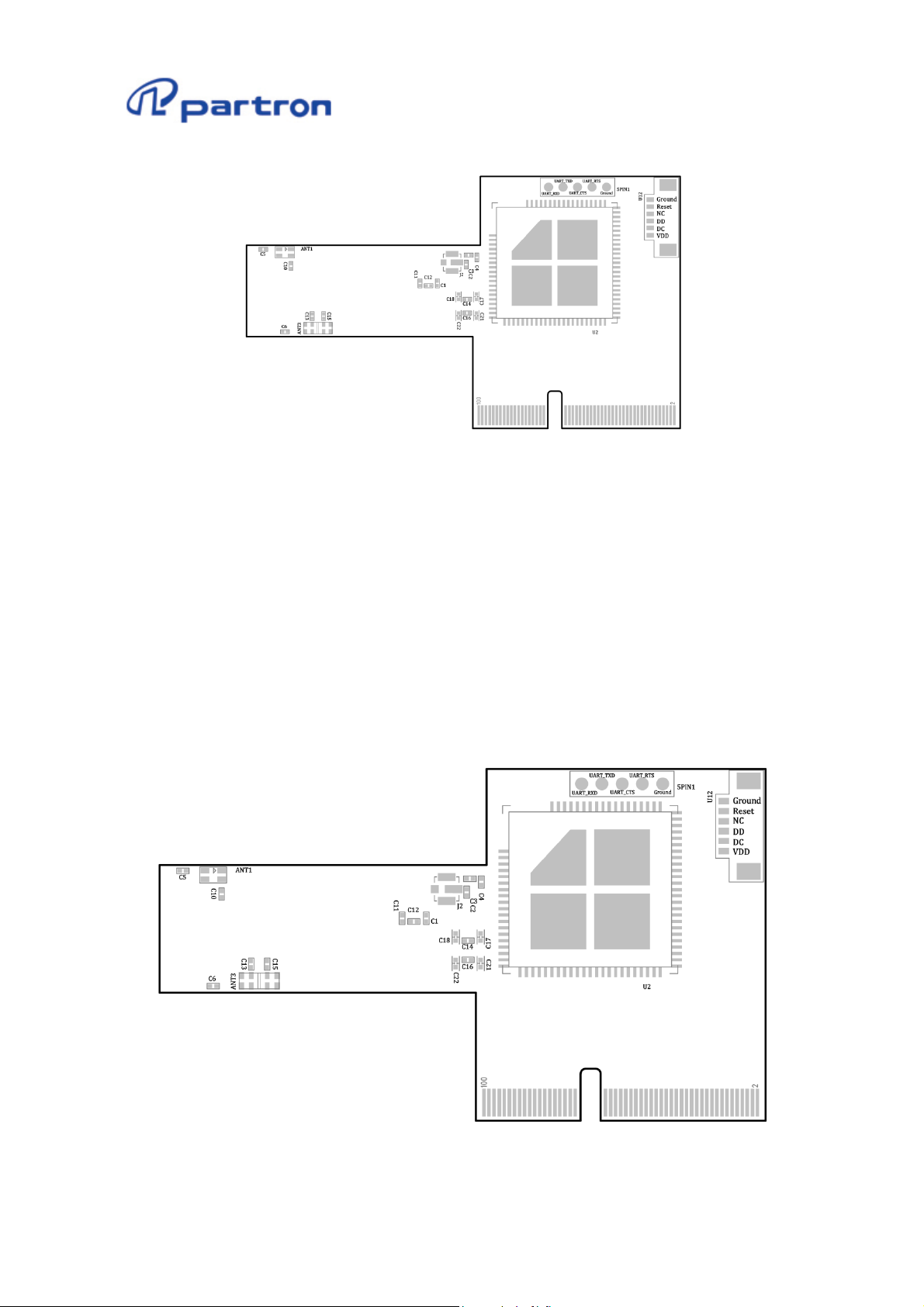
Shows the CZ3730A-COM8 EVB
User Guide
Figure 1 CZ3730A-COM8 EVB(Top View)
1.1 General Features
The CZ3730A-COM8 EVB includes the following features:
WLAN, Bluetooth, BLE and Zigbee on a single module board
100-pin board card
Dimensions:76mm(L) x 44.02mm(W)
WLAN 2.4- and 5-GHz SISO(20- and 40-MHz channels), 2.4-GHz MIMO(20-MHz channels)
Support for BLE dual mode
Seamless integration with TI Sitara and Other application processors
Design for the TI AM335X General-purpose evaluation module (EVM)
WLAN and Bluetooth single-antenna coexistence
Built-in chip antenna
2. Board Pin Assignment
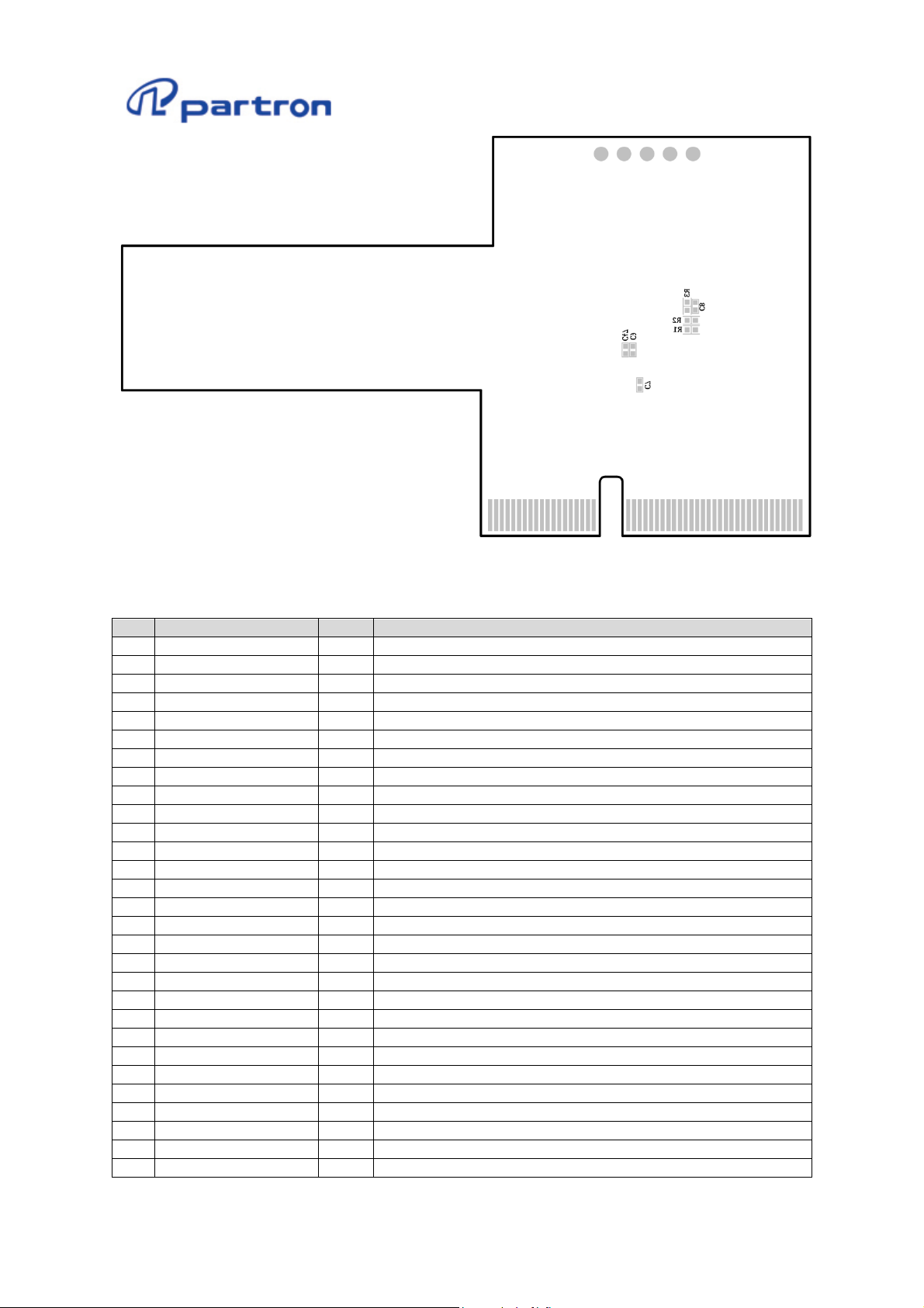
Shows the top view of the EVB
Show the bottom slide of the EVB
Figure 2 EVB Top (Top View)
User Guide
Figure 3 EVB Bottom (Top View)
2.1 Pin Description
No. Name Type Description
1 RTC_CLK I Slow clock input option (default: NU)
2 Ground G Ground
3 Ground G Ground
4 WLAN_EN_SOC I WLAN enable
5 VBAT_IN P 3.6-V typical voltage input
6 Ground G Ground
7 VBAT_IN P 3.6-V typical voltage input
8 VIO_IN P Vio 1.8-V (I/O voltage) input
9 Ground G Ground
10 N.C No connection
11 WL_RS232_TX O WLAN tool RS232 output
12 N.C No connection
13 WL_RS232_RX I WLAN tool RS232 input
14 N.C No connection
15 WL_UART_DBG O WLAN Logger output
16 N.C No connection
17 N.C No connection
18 Ground G Ground
19 Ground G Ground
20 SDIO_CLK_WL I WLAN SDIO clock
21 N.C No connection
22 Ground Ground
23 N.C No connection
24 SDIO_CMD_WL I/O WLAN SDIO command
25 N.C No connection
26 SDIO_D0_WL I/O WLAN SDIO data bit 0
27 N.C No connection
28 SDIO_D1_WL I/O WLAN SDIO data bit 1
29 N.C No connection
User Guide
30 SDIO_D2_WL I/O WLAN SDIO data bit 2
31 N.C No connection
32 SDIO_D3_WL I/O WLAN SDIO data bit 3
33 N.C No connection
34 WLAN_IRQ O WALN SDIO interrupt out
35 N.C No connection
36 N.C No connection
37 Ground G Ground
38 N.C No connection
39 N.C No connection
40 N.C No connection
41 N.C No connection
42 Ground G Ground
43 N.C No connection
44 N.C No connection
45 N.C No connection
46 N.C No connection
47 Ground G
48 N.C No connection
49 N.C No connection
50 N.C No connection
51 N.C No connection
52 BT_AUD_CLK I/O Bluetooth PCM clock input of output
53 N.C No connection
54 BT_AUD_FSYNC I/O Bluetooth PCM frame sync input of output
55 N.C No connection
56 BT_AUD_IN I Bluetooth PCM data input
57 N.C No connection
58 BT_AUD_OUT O Bluetooth PCM data output
59 N.C No connection
60 Ground G Ground
61 N.C No connection
62 N.C No connection
63 Ground G Ground
64 Ground G Ground
65 N.C No connection
66 BT_HCI_TX O Bluetooth HCI UART transmit output
67 N.C No connection
68 BT_HCI_RX I Bluetooth HCI UART receive input
69 N.C No connection
70 BT_HCI_CTS I Bluetooth HCI UART Clear to Send input
71 N.C No connection
72 BT_HCI_RTS O Bluetooth HCI UART Request to Send output
73 N.C No connection
74 N.C No connection
75 N.C No connection
76 BT_UART_DBG O Bluetooth Logger UART output
77 Ground G Ground
78 N.C No connection
79 N.C No connection
80 N.C No connection
81 N.C No connection
82 N.C No connection
83 Ground G Ground
84 N.C No connection
85 N.C No connection
86 N.C No connection

User Guide
87 Ground G Ground
88 N.C No connection
89 N.C No connection
90 N.C No connection
91 N.C No connection
92 Ground G Ground
93 N.C No connection
94 N.C No connection
95 Ground G Ground
96 GPIO11 I/O General-purpose I/O
97 Ground G Ground
98 N.C No connection
99 N.C No connection
100 N.C No connection
3. CZ3730A Module Electrical Characteristics
3.1 DC characteristics
Recommended Operating Conditions
Symbol Parameter Min. Nom. MAX. Unit
VBAT 2.9 3.3 3.7 V
VIO 1.62 1.8 1.92 V
LS_VIO 3.3 5 V
3.2 External Slow clock Input (RTC Clock)
The external slow clock input should be present at all times. The slow clock is used to maintain timers that
synchronize the device to the access point beacons.
Slow Clock is a digital square-wave in the range of 0`1.8V nom.
Parameter Condition Sym Min. Nom. MAX. Unit
Input slow clock frequency 32768 Hz
Input slow clock accuracy
(Initial + temp + aging)
Input transition time Tr/Tf-10%
to 90%
Frequency input duty cycle 15 50 85 %
Input voltage limits
Input impedance 1 MΩ
Input capacitance 5 pF
WLAN,BT ±250
ANT ±50
Tr/Tf 100 ns
Square wave
DC-coupled
Vih
Vil 0 0.35xVIO
0.65
xVIO
VIO
ppm
Vpeak

User Guide
3.3 1.8V I/O Operation Condition
Parameter Condition Sym Min Max Unit PIN
IO High-level input voltage VIH
IO low-level input voltage VIL
Enable inputs high-level input
voltage
Enable inputs low-level input
voltage
High-level output voltage
Low-Level output voltage
Input transitions time Tr/Tf from
10% to 90% (Digital IO)
Output rise time from 10% to
90% (Digital IO)
Output fall time from 10% to
90% (Digital IO)
Vih_en
Vil_en 0 0.4
@4mA
@1mA
@0.3mA
@4mA
@1mA
@0.09mA
CL < 25pF Tr 4.9 ns
CL < 25pF Tf 5.3 ns
VOH
VOL
Tr/Tf
0.65x VIO
0
1.365
VIO-0.45
VIO-0.112
VIO-0.033
0
0
0
1 10 ns
VIO
0.35xVIO
VIO
VIO
VIO
VIO
0.45
0.112
0.01
V
24pin,
25pin
26pin,
27pin
28pin,
29pin
30pin
3.4 3.3V I/O Operation Condition
Ta = 25, VBAT=3V, unless otherwise noted.
Parameter Test Condition MIN TYP MAX Unit
Logic-0 input voltage
Logic-1 input voltage
Logic-0 output voltage 4-mA pins
Logic-1 output voltage 4-mA pins
Logic-0 output voltage 20-mA pins
Logic-1 output voltage 20-mA pins
Output load 4mA
Output load 4mA
Output load 20mA
Output load 20mA
0.5
2.5
0.5
2.4
0.5
2.4
V

User Guide
3.5 WLAN 2.4-GHz current consumption (AT BT and ZIGBEE Disable )
Recommended Operating Conditions
Parameter Conditions Min. Nom. MAX. Unit
TX, 802.11b 11Mbps
TX, 802.11g 54Mbps
TX, 802.11n MCS7
TX, 802.11n MCS15
RX, 802.11b 11Mbps
RX, 802.11g 54Mbps
RX, 802.11n MCS7
RX, 802.11n MCS15
3.6 WLAN 5-GHz current consumption (AT BT and ZIGBEE Disable )
Maximum output power
Packet size = 400Byte, Delay 700uSec
Maximum output power
Packet size = 2000Byte, Delay 700uSec
Maximum output power
Packet size = 2000Byte, Delay 700uSec
Maximum output power
Packet size = 2000Byte, Delay 700uSec
At -85dBm
At -72dBm
At -70dBm
265 mA
193 mA
172 mA
195 mA
86 mA
94 mA
92 mA
TBD mA
Recommended Operating Conditions
Parameter Conditions Min. Nom. MAX. Unit
TX, 802.11a 54Mbps
TX, 802.11n MCS7
RX, 802.11a 54Mbps
RX, 802.11n MCS7
Maximum output power
Packet size = 2000Byte, Delay 700uSec
Maximum output power
Packet size = 2000Byte, Delay 700uSec
At -71dBm
At -69dBm
167 mA
158 mA
80 mA
74 mA
3.7 Bluetooth 4.0 current consumption (AT WLAN and ZIGBEE Disable )
Recommended Operating Conditions
Parameter Conditions Min. Nom. MAX. Unit
TX, Basic mode
TX, EDR mode
RX, Basic mode
RX, EDR mode
Packet type = PRBS
EDR-3M
At -90dBm
At -82dBm, EDR-3M
73 mA
47 mA
42 mA
42 mA
3.8 Bluetooth Low Energy Current consumption (AT WLAN and ZIGBEE Disable )
Recommended Operating Conditions
Parameter Conditions Min. Nom. MAX. Unit
TX
RX
Packet type = PRBS
At -90dBm
60 mA
49 mA

User Guide
3.9 Bluetooth Low Energy Current consumption (AT WLAN and ZIGBEE Disable )
Recommended Operating Conditions
Parameter Conditions Min. Nom. MAX. Unit
TX
RX
Modulated, Continuous TX,
52 mA
43 mA
3.10 2.4GHz WLAN RF specification
Parameter Conditions Min. Nom. MAX. Unit
Operation frequency range 2412 2462 MHz
Linear output power in 802.11b mode
1~11Mbps(ch1~11)
Packet Size =2000byte
Delay = 400usec
Linear output power in 802.11g mode
6~54Mbps(ch1,11)
6~54Mbps(ch2~10) 15 16 dBm
Packet Size =2000byte
Delay = 400usec
Linear output power in 802.11n mode
HT20,MCS0~7(ch1,11)
HT20,MCS0~7(ch2~10) 15 16 dBm
HT20,MCS8~15(ch1,11) 13.5 14.5 dBm
HT20,MCS8~15(ch2~10) 15.5 16.5 dBm
HT40,MCS0~7(ch3,9) 10.5 11.5 dBm
HT40,MCS0~7(ch4~8) 13.5 14.5 dBm
Packet Size =2000byte
Delay = 400usec
Transmit spectrum mask
Margin to 802.11b spectrum mask
Margin to 802.11g spectrum mask
Margin to 802.11n spectrum mask
Maximum output power
Transmit modulation accuracy in 802.11b mode
1~11Mbps
As specified in IEEE 802.11b
Transmit modulation accuracy in 802.11g mode
6Mbps
54Mbps -26 dB
Maximum output power
Transmit modulation accuracy in 802.11n mode
HT20, MCS0
HT20, MCS7 -28 dB
HT20, MCS15 -28 dB
Maximum output power
15 16 dBm
12 13 dBm
12 13 dBm
1 dB
5 dB
5 dB
35 %
-16 dB
-17 dB
Parameter Conditions Min. Nom. MAX. Unit
Transmit power-on and power-down ramp time in 802.11b mode
Transmit power-on ramp time
From 10% to 90% output power
Transmit power-down ramp time
From 90% to 10% output power
2 usec
2 usec

User Guide
3.11 5GHz WLAN specification
Parameter Conditions Min. Nom. MAX. Unit
Linear output power in 802.11a mode
6~54Mbps
(ch36,40,44,48,149,165)
6~54Mbps
(ch153,157,161)
Packet Size =2000byte
Delay = 400usec
12.5 13.5 dBm
14.5 15.5 dBm
Linear output power in 802.11n mode
HT20,MCS0~7
(ch36,40,44,48,149,165)
HT20,MCS0~7
(ch153,157,161)
HT40, MCS0~7
(ch38,151)
HT40, MCS0~7
(ch46,159)
Packet Size =2000byte
Delay = 400usec
12.5 13.5 dBm
14.5 15.5 dBm
9 10 dBm
13 14 dBm
Transmit spectrum mask
Margin to 802.11a spectrum
mask
Margin to 802.11n spectrum
mask
Maximum output power
4 dB
4 dB
Transmit modulation accuracy in 802.11a mode
6Mbps
54Mbps -26 dB
Maximum output power
-19 dB
Transmit modulation accuracy in 802.11n mode
HT20, MCS0
HT20, MCS7 -28 dB
HT40, MCS0 -20 dB
HT40, MCS7 -28 dB
Maximum output power
-20 dB

User Guide
3.12 Bluetooth 4.0 RF Specificaiton
Parameter Conditions Min. Nom. MAX. Unit
Bluetooth Specification Bluetooth 4.0 Classic 1
Power Class Class 1
Frequency range 2402 2480 MHz
Channel Spacing 1 MHz
BDR Transmitter
RF transmit power 12 13 dBm
Initial carrier frequency -75 75 kHz
Carrier frequency drift Drift rate -2.3
∆flavg 161 kHz
Modulation characteristics
∆f2max 133 kHz
∆f2avg/∆f1avg 8.2 %
kHz/5
0㎲
EDR Transmitter
RF transmit power 7 8 dBm
3.15 Bluetooth Low Energy RF Specification
Parameter Conditions Min. Nom. MAX. Unit
Bluetooth Specification Bluetooth Low Energy
Frequency range 2402 2480 MHz
Channel Spacing 2 MHz
BLE Transmitter
RF transmit power 9 10 dBm
Initial carrier frequency -4 kHz
Carrier frequency drift Drift rate 2
Modulation characteristics
∆flavg 247 kHz
∆f2avg/∆f1avg 0.82 %
kHz/50㎲
3.16 Zigbee RF Specification
Parameter Conditions Min. Nom. MAX. Unit
Operation frequency range 2402 2480 MHz
Maximum RF Transmit Power 2 3 dBm
Frequency Tolerance -96 +96 kHz
Error Vector Magnitude 35 %

4. Antenna Characteristics
Show the antenna VSWR characteristics.
User Guide

5. Circuit Design
5.1 EVB Reference Schematics
User Guide

User Guide
6. FCC Approval
-Caution
Any changes or modifications not expressly approved by the party responsible for compliance could void the user’s
authority to operate this device.
This device complies with Part 15 of the FCC`s Rules. Operation is subject to the following two Conditions:
1. This device may not cause harmful interference, and
2. This device must accept any interference received, including interference that may cause undesirable operation.
This device generates, uses and can radiate radio frequency energy and, if not installed and used in accordance
with the instructions, may cause harmful interference to radio communications. However, there is no guarantee
that interference will not occur in a particular installation. If this equipment does cause harmful interference to radio
or television reception, which can be determined by turning the equipment off and on, the user is encouraged to try
to correct the interference by one or more of the following measures:
– Reorient or relocate the receiving antenna.
– Increase the separation between the equipment and receiver.
– Connect the equipment into an outlet on a circuit different from that to which the receiver is connected.
– Consult the dealer or an experienced radio/TV technical for help.
This device complies with FCC radiation exposure limits set forth for an uncontrolled environment.
This device should be installed and operated with minimum distance 20cm between the radiating element of this
device and the user.
This device must not be co-located or operating in conjunction with any other antenna or transmitter.
This device may only operate using an antenna of a type and maximum (or lesser) gain approved by partron.
Antenna types not included in the list, having a gain greater than the maximum gain indicated for that type, are
strictly prohibited for use with this transmitter.
Note
Function (ANT A)
WLAN(2.4/5GHz), Blutooth -1.07 dBi 1.16 dBi -0.08 dBi
Function (ANT B)
WLAN(2.4GHz Only) 1.63 dBi X X
In the event that these conditions cannot be met then the FCC authorization is no longer considered valid and the
FCC ID cannot be used on the final product.
The satisfy FCC exterior labeling requirements, the following text must be placed on the exterior of the end product.
Contains Transmitter module FCC ID: 2AD5K-CZ3730A
This device is restricted to indoor use only within the 5150~5250MHz band.
2402~2480MHz 5180~5240 MHz 5745~5825 MHz
Peak Gain(Chip Antenna)
2412~2462 MHz X X
Peak Gain(Chip Antenna)
 Loading...