

Partner Tech International PT-5700 Service Manual
PT-5700
Service Manual


Copyright
This publication, including all photographs, illustrations and software, is protected under international copyright laws,
with all rights reserved. Neither this manual, nor any of the material contained herein, may be reproduced without written consent of the author.
Disclaimer
The information in this document is subject to change without notice. The manufacturer makes no representations or
warranties with respect to the contents hereof and specifically disclaims any implied warranties of merchantability or
fitness for any particular purpose. The manufacturer reserves the right to revise this publication and to make changes
from time to time in the content hereof without obligation of the manufacturer to notify any person of such revision or
changes.
Trademark recognition
TouchKit is either a registered trademark or trademark of eGalex Incorporated.
TouchWare is either a registered trademark or trademark of 3M.
VIA and Hyperion are either registered trademarks or trademarks of VIA Technologies Incorporated.
All other product names used in this manual are the properties of their respective owners and are acknowledged.
Federal Communications Commission (FCC)
This equipment has been tested and found to comply with the limits for a Class A digital device, pursuant to Part 15 of
the FCC Rules. These limits are designed to provide reasonable protection against harmful interference in a residential
installation. This equipment generates, uses, and can radiate radio frequency energy and, if not installed and used in
accordance with the instructions, may cause harmful interference to radio communications. However, there is no guarantee that interference will not occur in a particular installation. If this equipment does cause harmful interference to
radio or television reception, which can be determined by turning the equipment off and on, the user is encouraged to
try to correct the interference by one or more of the following measures:
• Reorient or relocate the receiving antenna.
• Increase the separation between the equipment and the receiver.
• Connect the equipment onto an outlet on a circuit different from that to which the receiver is connected.
• Consult the dealer or an experienced radio/TV technician for help.
Shielded interconnect cables and a shielded AC power cable must be employed with this equipment to ensure compliance with the pertinent RF emission limits governing this device. Changes or modifications not expressly approved by
the system's manufacturer could void the user's authority to operate the equipment.
Declaration of conformity
This device complies with part 15 of the FCC rules. Operation is subject to the following conditions:
• This device may not cause harmful interference, and
• This device must accept any interference received, including interference that may cause undesired operation.
i

About this manual
The service manual provides service information for the PT-5700 POS. This manual is designed to help trained service
personnel to locate and fix failing parts on the PT-5700.
This manual consists of the following sections:
Chapter 1 Getting Started: This section provides general information on the
PT-5700, a packing list, and illustrations to identify components.
Chapter 2 BIOS Setup Utility: The BIOS chapter provides information on navi-
gating and changing settings in the BIOS Setup
Utility.
Chapter 3 Installing Drivers and Software: This chapter provides information on installing
drivers for supported operating systems.
Chapter 4 Locating the Problem: Refer to this chapter to locate the failing part or
cause of the problem that requires servicing.
Chapter 5 Replacing Field Replaceable Units (FRUs): This chapter provides drawings and instructions
to replace all FRUs.
Appendix Exploded Diagrams and Parts List: The appendix includes an exploded diagram of
the PT-5700 and the parts list and order number
for each part.
Safety information
Before servicing the PT-5700, read the safety information under “Safety and precautions” on page 55.
Revision history
Version 1.0, June 2007
ii

TABLE OF CONTENTS
Chapter 1
Getting Started .................................................................................................................. 1
Unpacking and listing the PT-5700 contents ...................................................................................... 1
Identifying components ...................................................................................................................... 2
Front-right view ................................................................................................................................................. 2
Rear-right view .................................................................................................................................................. 3
Rear connectors .................................................................................................................................................4
Removing the rear cover ..................................................................................................................... 5
Chapter 2
BIOS Setup Utility ...........................................................................................................7
About the Setup Utility ....................................................................................................................... 7
Entering the Setup Utility .................................................................................................................................. 8
BIOS navigation keys ......................................................................................................................................... 8
Using BIOS ....................................................................................................................................................... 9
Standard CMOS features .................................................................................................................... 9
IDE Primary/Secondary Master/Slave ............................................................................................................. 9
Advanced BIOS Features ................................................................................................................. 11
Advanced Chipset Features ............................................................................................................................. 13
DRAM Clock/Drive Control ............................................................................................................................ 14
AGP & P2P Bridge Control ............................................................................................................................ 17
CPU & PCI Bus Control ................................................................................................................................. 17
Integrated Peripherals ...................................................................................................................... 19
VIA OnChip IDE Device .................................................................................................................................. 21
VIA OnChip PCI Device .................................................................................................................................. 22
SuperIO Device ................................................................................................................................................ 23
Power Management Setup Option .................................................................................................... 24
PnP/PCI Configurations .................................................................................................................................. 28
PC Health Status .............................................................................................................................................. 30
Frequency/Voltage Control ............................................................................................................... 31
Other BIOS Options ......................................................................................................................................... 32
Load Fail-Safe Defaults Option ....................................................................................................................... 32
Load Optimized Defaults Option ..................................................................................................................... 32
Set Supervisor and User Passwords Options .................................................................................................. 33
Save & Exit Setup Option ................................................................................................................................ 33
Exit Without Saving ........................................................................................................................................ 33
Chapter 3
Installing Drivers and Software ......................................................................................35
Driver auto installation ..................................................................................................................... 35
Chipset driver .................................................................................................................................... 36
Display driver ................................................................................................................................... 38
Audio driver ...................................................................................................................................... 39
LAN driver ........................................................................................................................................ 41
Touch screen driver .......................................................................................................................... 43
iii

Chapter 4
Locating the Problem .....................................................................................................47
General checkout guidelines ............................................................................................................. 47
Power system checkout ..................................................................................................................... 47
Cash drawer checkout ....................................................................................................................... 48
LCD symptoms ................................................................................................................................. 49
Touch screen symptoms .................................................................................................................... 49
Power symptoms ............................................................................................................................... 50
Network symptoms ........................................................................................................................... 50
USB symptoms ................................................................................................................................. 51
MSR reader symptoms ...................................................................................................................... 51
Boot symptoms ................................................................................................................................. 51
Peripheral-device symptoms ............................................................................................................. 52
Motherboard and PCB board jumper settings ................................................................................... 52
Setting a jumper ............................................................................................................................................... 52
Motherboard jumpers and connectors ............................................................................................................. 53
Chapter 5
Replacing Field Replaceable Units (FRUs) ...................................................................55
Safety and precautions ...................................................................................................................... 55
Before you begin ............................................................................................................................... 56
Replacing Parts ................................................................................................................................. 56
Rear base cover ............................................................................................................................................... 57
Front base cover .............................................................................................................................................. 58
Customer display ............................................................................................................................................. 59
HDD bracket .................................................................................................................................................... 60
HDD ................................................................................................................................................................. 60
I/O PCB ........................................................................................................................................................... 61
MSR .................................................................................................................................................................. 62
CF card PCB ................................................................................................................................................... 64
Inverter ............................................................................................................................................................ 65
VFD-T .............................................................................................................................................................. 66
Mainboard ....................................................................................................................................................... 67
Touch control ................................................................................................................................................... 69
Front display cover .......................................................................................................................................... 70
Touch panel ..................................................................................................................................................... 71
LCD panel ........................................................................................................................................................ 73
Appendix
Exploded Diagrams and Parts List .................................................................................75
Main parts ......................................................................................................................................... 75
List of Parts FRUs ............................................................................................................................. 75
Display Parts and Cables .................................................................................................................. 78
List of Cables FRUs .......................................................................................................................... 79
iv

TABLE OF FIGURES
Figure 1.1 Unpacking/repacking the PT-5700...............................................................................1
Figure 1.2 Front-right view of PT-5700 ........................................................................................2
Figure 1.3 Rear-right view of PT-5700 .........................................................................................3
Figure 1.4 Connectors with cables disconnected ..........................................................................4
Figure 2.1 Main BIOS menu .........................................................................................................8
Figure 2.2 Standard CMOS Features menu...................................................................................9
Figure 2.3 IDE Primary Master Submenu .....................................................................................10
Figure 2.4 Advanced Chipset Features menu ................................................................................13
Figure 2.5 DRAM Clock/Drive Control menu ..............................................................................14
Figure 2.6 AGP & P2P Bridge Control menu ...............................................................................17
Figure 2.7 CPU & PCI Bus Control menu ....................................................................................18
Figure 2.8 Integrated Peripherals menu.........................................................................................19
Figure 2.9 VIA OnChip IDE Device menu ...................................................................................21
Figure 2.10 VIA OnChip PCI Device menu....................................................................................22
Figure 2.11 Super I/O Device menu ................................................................................................23
Figure 2.12 Power Management Setup menu..................................................................................24
Figure 2.13 IRQ/Event Activity Detect menu .................................................................................26
Figure 2.14 IRQs Activity Monitoring menu ..................................................................................28
Figure 2.15 PnP/PCI Configurations menu .....................................................................................28
Figure 2.16 PC Health Status menu.................................................................................................30
Figure 2.17 Frequency/Voltage Control menu ................................................................................31
Figure 3.1 Driver CD autoinstall screen ........................................................................................35
Figure 4.1 Connecting a cash drawer ............................................................................................48
Figure 4.2 Mainboard jumper settings...........................................................................................53
Figure 6.1 Exploded diagram main parts.......................................................................................75
Figure 6.2 Exploded diagram cables .............................................................................................78
v

vi
CHAPTER 1
G
ETTING STARTED
This chapter describes the preparation before servicing the PT-5700. The following topics are described.
• “Unpacking and listing the PT-5700 contents”
• “Identifying components” on page 2
• “Removing the rear cover” on page 5
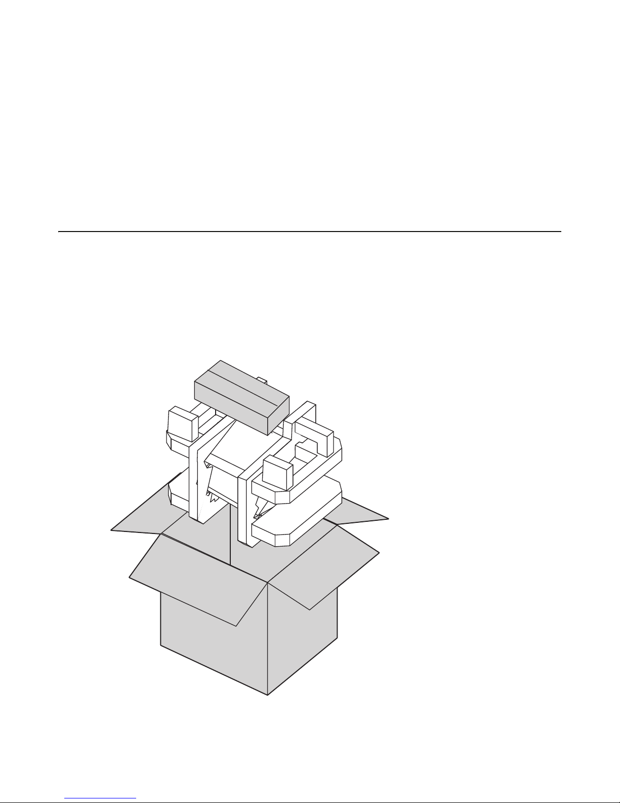
Unpacking and listing the PT-5700 contents
If the PT-5700 is returned for servicing in its original packing, save the packing materials for return to the customer.
List and ensure that after you finish servicing, the items you unpack are repacked as shown in Figure 1.1.
• PT-5700
• Power cable and adapter
•Customer display
•Other
Figure 1.1 Unpacking/repacking the PT-5700
1
Identifying components
1 2 3
This section describes the parts and connectors on the PT-5700.
Front-right view
Figure 1.2 Front-right view of PT-5700
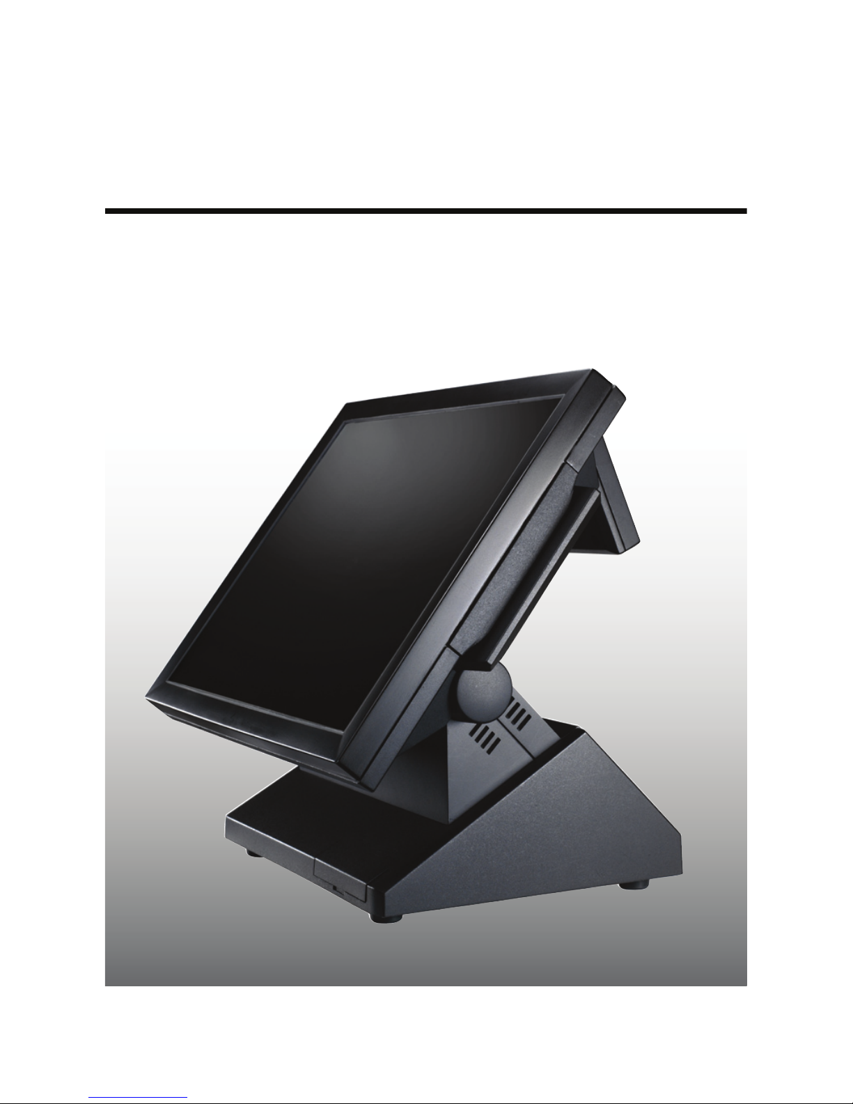
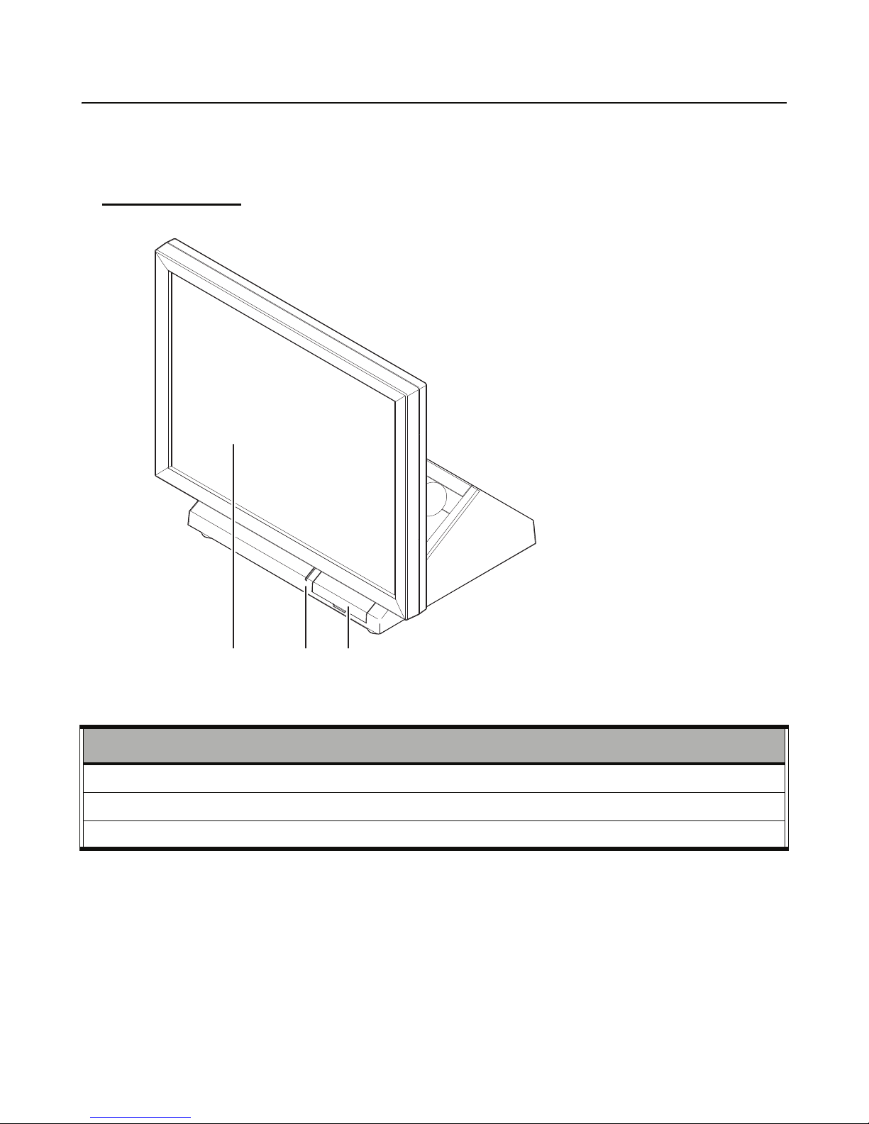
1 15-inch TFT LCD touch screen
2 Power LED
3 Power button/USB cover
2 Getting Started
DESCRIPTION
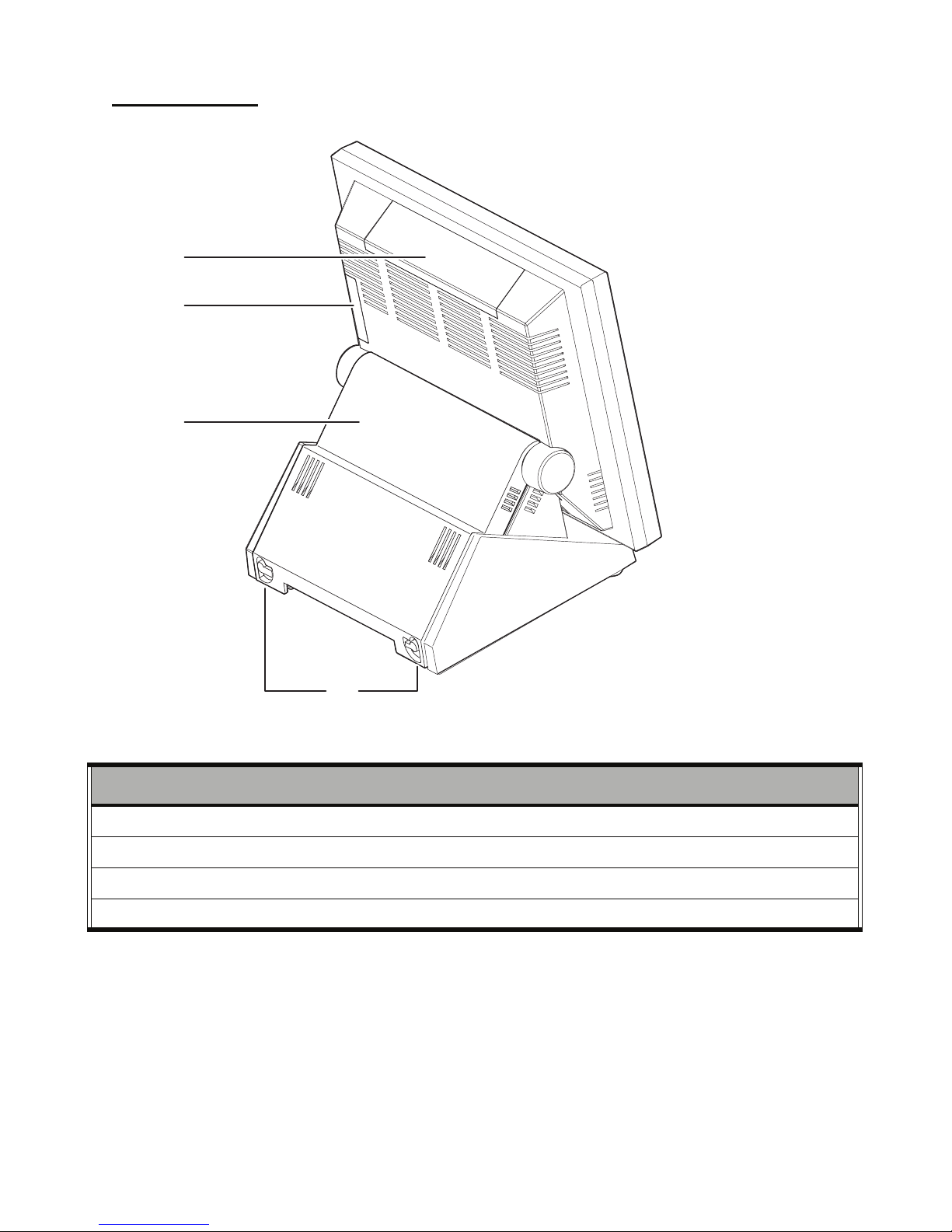
Rear-right view
4
3
2
1
Figure 1.3 Rear-right view of PT-5700
1 Customer display cover
2 Magnetic card reader cover
3 Rear cover
4 Rear cover latches
DESCRIPTION
Identifying components 3
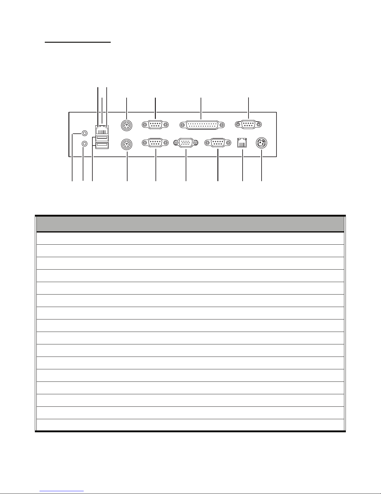
Rear connectors
12 3
5
4
67
14
16
13
15
12 11 10 9 8
Figure 1.4 shows the connectors on the rear of the PT-5700. You must remove the rear cover to access the connectors.
See “Removing the rear cover” on page 5.
Figure 1.4 Connectors with cables disconnected
1 RJ-45 connector
2 PS/2 mouse connector
3 COM 3 connector
4 Parallel connector
5 COM 2 connector
6 Green act LED
7 Orange link LED
8 Power connector
9 RJ-11 connector
10 COM 1 connector
11 VGA connector
12 COM 4 connector
13 PS/2 keyboard connector
14 USB connectors
DESCRIPTION
15 Mic in connector
16 Audio out connector
4 Getting Started
1. There are two more USB connectors on the front of the PT-5700.
NOTE
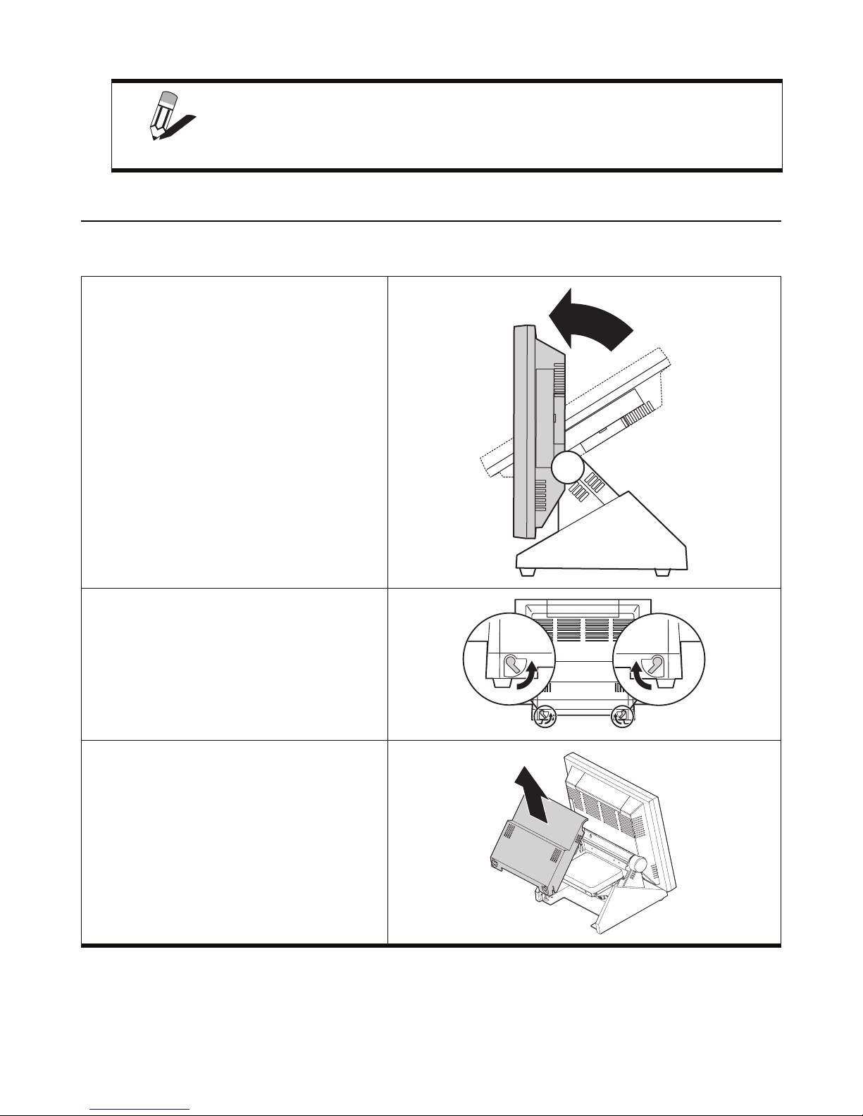
Removing the rear cover
Refer to the following to remove the rear cover.
1 Rotate the display until it’s perpendicular.
2 Open the rear cover latches.
3 Remove the rear cover.
Removing the rear cover 5

6 Getting Started

CHAPTER 2
TIP
BIOS S
The BIOS (Basic Input and Output System) Setup Utility displays the system's configuration status and provides
options to set system parameters. The parameters are stored in battery-backed-up CMOS RAM that saves this information even when the power is turned off. When the system is turned back on, the system is configured with the values
found in CMOS.The following topics are described in this chapter.
• “About the Setup Utility”
• “Entering the Setup Utility” on page 8
• “Standard CMOS features” on page 9
• “Advanced BIOS Features ” on page 11
• “Integrated Peripherals ” on page 19
• “Power Management Setup Option” on page 24
• “PnP/PCI Configurations” on page 28
• “PC Health Status” on page 30
• “Frequency/Voltage Control” on page 31
• “Other BIOS Options” on page 32
ETUP UTILITY
About the Setup Utility
The BIOS Setup Utility enables you to configure the following items:
• Hard drives, diskette drives, and peripherals
• Video display type and display options
• Password protection from unauthorized use
• Power management features
If you have made settings that you do not want to save, use the "Exit Without
Saving" item and press Y to discard any changes you have made.
This Setup Utility should be used for the following:
• When changing the system configuration
• When a configuration error is detected and you are prompted to make changes to the Setup Utility
• When trying to resolve IRQ conflicts
• When making changes to the Power Management configuration
• When changing the User or Supervisor password
7
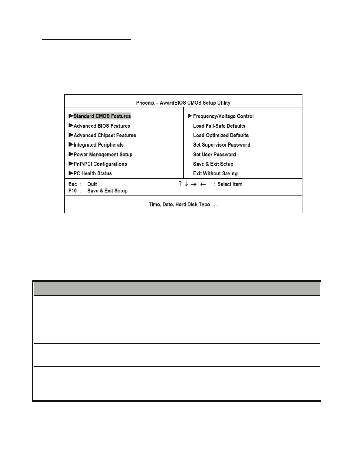
Entering the Setup Utility
When you power on the system, BIOS enters the Power-On Self Test (POST) routines. POST is a series of built-in
diagnostics performed by the BIOS. After the POST routines are completed, the following message appears:
Press DEL to enter SETUP
Press the delete key <Delete> to access the Award BIOS Setup Utility:
Figure 2.1 Main BIOS menu
BIOS navigation keys
The BIOS navigation keys are listed below.
KEY FUNCTION
←↑↓→
+/–/PU/PD Modifies the selected field's values
Esc Exits the current menu
F1 Displays a screen that describes all key functions
F5 Loads previously saved values to CMOS
F6 Loads a minimum configuration for troubleshooting
F7 Loads an optimum set of values for peak performance
F10 Saves the current configuration and exits Setup
Scrolls through the items on a menu
Shift + F2 Changes the color of the BIOS menu
8 BIOS Setup Utility
Using BIOS
When you start the Setup Utility, the main menu appears. The main menu of the Setup Utility displays a list of the
options that are available. A highlight indicates which option is currently selected. Use the cursor arrow keys to move
the highlight to other options. When an option is highlighted, execute the option by pressing <Enter>.
Some options lead to pop-up dialog boxes that prompt you to verify that you wish to execute that option. Other options
lead to dialog boxes that prompt you for information.
Some options (marked with a triangle ) lead to submenus that enable you to change the values for the option. Use the
cursor arrow keys to scroll through the items in the submenu.
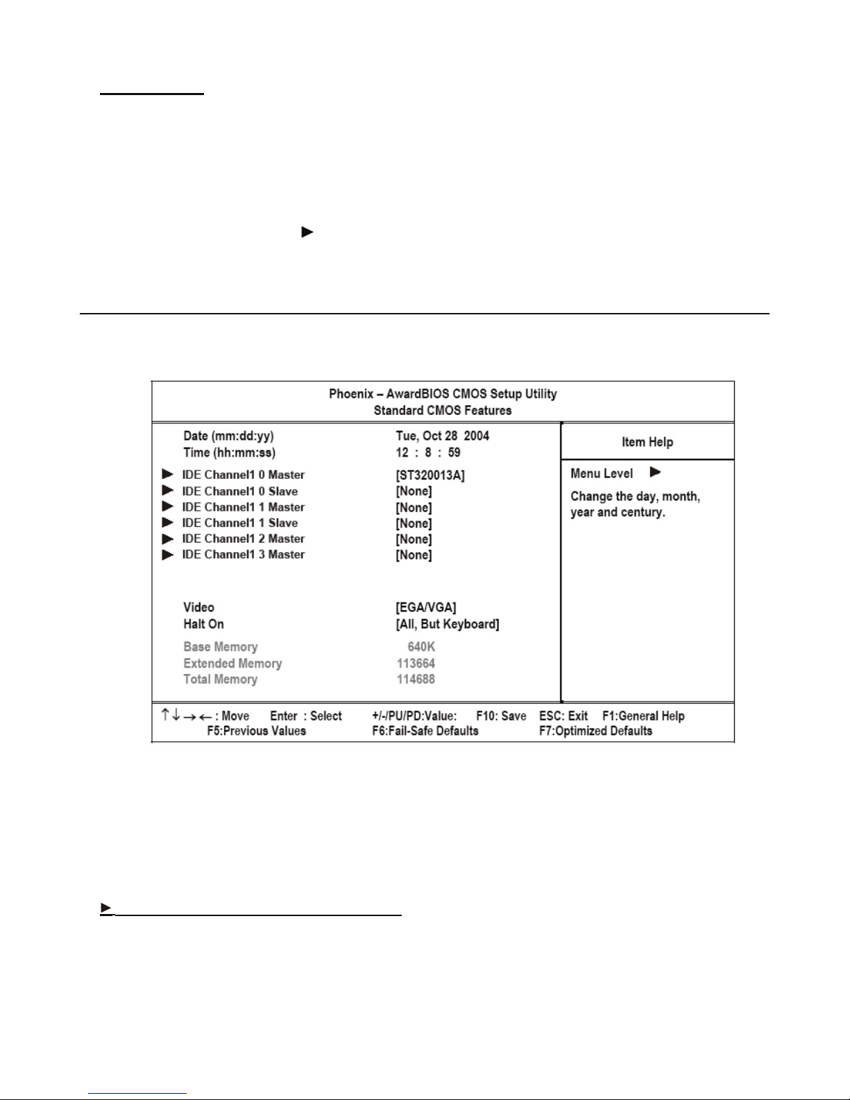
Standard CMOS features
Selecting Standard CMOS Features on the main menu displays the following menu:
Figure 2.2 Standard CMOS Features menu
Date and Time
The Date and Time items show the current date and time held by the PT-5700. If you are running a Windows OS, these
items are automatically updated whenever you make changes to the Windows Date and Time Properties utility.
IDE Primary/Secondary Master/Slave
This field is used to configure the IDE hard drive installed in the system. Move the cursor to highlight the IDE Primary/Secondary Master/Slave fields and press <Enter>. The IDE Primary Master submenu opens:
Standard CMOS features 9
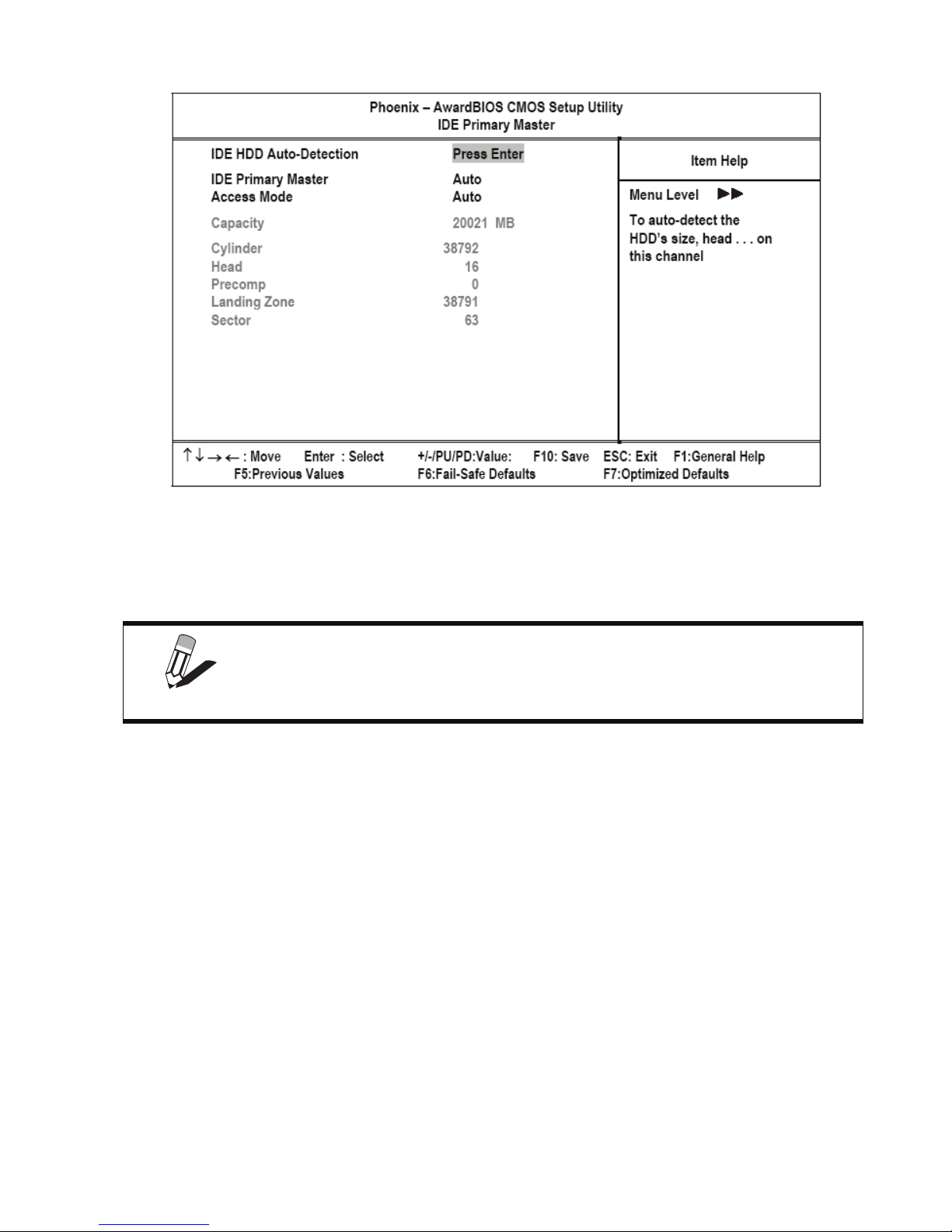
Figure 2.3 IDE Primary Master Submenu
IDE HDD Auto-Detection
Press Enter while this item is highlighted if you want the Setup Utility to automatically detect and configure a hard
disk drive on the IDE channel.
If you are setting up a new hard disk drive that supports LBA mode, more than
one line will appear in the parameter box. Choose the line that lists LBA for an
NOTE
IDE Primary/Secondary Master/Slave
LBA drive.
If you leave this item at Auto, the system will automatically detect and configure any IDE devices it finds. If it fails to
find a hard disk, change the value to Manual and then manually configure the drive by entering the characteristics of
the drive in the fields described below:
• Capacity – displays the capacity of the HDD in megabytes (MB).
• Cylinder – indicates the number of cylinders that the HDD has. A cylinder is the sum total of all tracks that are
in the same location on every disk surface.
• Head – displays the number of heads in the HDD. A head is a device that reads and writes data on the hard
disk.
• Precomp – displays the track where precompensation is initiated. Precompensation is a feature whereby the
HDD uses a stronger magnetic field to write data in sectors that are closer to the center of the disk. In CAV
recording, in which the disk spins at a constant speed, the sectors closest to the spindle are packed tighter than
the outer sectors.
• Landing Zone – displays the location of the safe non-data area on a hard disk that is used for parking the read/
write head.
• Sector – displays the number of sectors available on the HDD. A sector is the smallest unit of storage space on
a disk.
10 BIOS Setup Utility
Access Mode
This item defines special ways that can be used to access IDE hard disks such as LBA (Large Block Addressing).
Leave this value at Auto and the system will automatically decide the fastest way to access the hard disk drive.
Press <Esc> to close the IDE device sub-menu and return to the Standard CMOS Features menu.
Video
This item defines the video mode of the system. This mainboard has a built-in VGA graphics system; you must leave
this item at the default setting.
Halt On
This item defines the operation of the system POST (Power On Self Test) routine. You can use this item to select which
types of errors in the POST are sufficient to halt the system.
Base Memory, Extended Memory, and Total Memory
These items are automatically detected by the system at start up time. These are display-only fields. You cannot make
changes to these fields.
• Base Memory – This field displays the amount of conventional memory detected by the system during boot.
• Extended Memory – This field displays the amount of extended memory detected by the system during boot.
• Tot a l M e mo r y – This field displays the total amount of memory (Base and Extended) detected by the system
during boot.
Press <Esc> to return to the main menu.
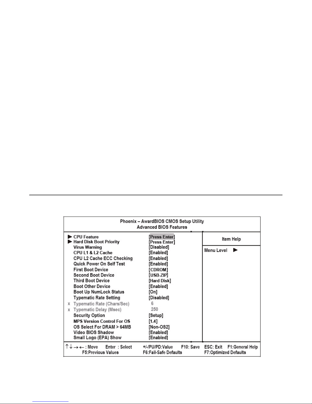
Advanced BIOS Features
Selecting Advanced BIOS Features on the main menu displays this menu:
Advanced BIOS Features 11

CPU Feature
• Delay Prior to Thermal -The Delay Prior To Thermal BIOS feature controls the activation of the Thermal
Monitor's automatic mode. It allows you to determine when the CPU's Thermal Monitor should be activated in
automatic mode after the system boots. For example, with the default value of 16 Minutes, the BIOS activates
the Thermal Monitor in automatic mode 16 minutes after the system starts booting up.
• Thermal Management - This item enables you to specify the Thermal Monitor1 (On die throtting) or Thermal
Monitor 2 (Ratio & VID transition). Default setting is Thermal Monitor 1.
•TM2 Bus Ratio - This represents the throttle frequency for the Trimedia TM2 PCI bus interface. Enter any
integer number between 0 and 255 inclusive to set this frequency..
• TM2 Bus VID - This represents the throttle voltage for the Trimedia TM2 PCI bus interface. Choose a value
between 0.8375V and 1.6000V inclusive.
Hard Disk Boot Priority
Select boot sequence for onboard or bootable Add-in cards.
Virus Warning
When enabled, this item provides protection against viruses that try to write to the boot sector and partition table of the
hard disk drive. You need to disable this item when installing an operating system. We recommend that you enable
anti-virus protection as soon as you have installed an operating system. The default setting is Disabled.
CPU L1 & L2 Cache
All processors that can be installed in this mainboard use internal level 1 (L1) and level 2 (L2) cache memory to
improve performance. Leave this item at the default setting for better performance. The default setting is Enabled.
CPU L2 Cache ECC Checking
This item enables or disables ECC (Error Correction Code) error checking on the CPU cache memory. We recommend
that you leave this item at the default setting. The default setting is Enabled.
Quick Power On Self Test
Enable this item to shorten the power on testing (POST) and have the system start up faster. You can enable this item
after you are confident that the system hardware is operating smoothly. The default setting is Enabled.
First/Second/Third Boot Device
The BIOS loads the operating system from the disk drives in the sequence selected in these three fields. The default
setting is CD-ROM/USB-ZIP/HDD0.
Boot Other Device
When enabled, the system searches all other possible locations for an operating system if it fails to find one in the
devices specified under the First, Second, and Third boot devices. The default setting is Enabled.
Boot Up NumLock Status
This item defines if the keyboard Num Lock key is active when the system is started. The default setting is On.
Typematic Rate Setting
If this item is enabled, you can use the following two items to set the typematic rate and the typematic delay settings
for the keyboard. The default setting is Disabled.
Typematic Rate (Chars/Sec)
Use this item to define how many characters per second are generated by a held-down key. The default setting is 6.
Typematic Delay (Msec)
Use this item to define how many milliseconds must elapse before a held-down key begins generating repeat characters. The default setting is 250.
12 BIOS Setup Utility
Security Option
If you have installed password protection, this item defines if the password is required at system start up, or if it is only
required when a user tries to enter the Setup Utility. The default setting is Setup.
MPS Version Control for OS
This specifies the version of the Multiprocessor Specification (MPS) to be used. Version 1.4 has extended configuration tables to improve support for multiple PCI bus configurations and provide future expandability - use this for NT,
and possibly Linux. It is also required for a secondary PCI bus to work without the need for a bridge. Leave it as 1.1 for
older server Operating Systems. The default setting is 1.4MPS Version Control For O.S 1.4.
OS Select For DRAM > 64 MB
This item is only required if you have installed more than 64 MB of memory and you are running the OS/2 operating
system. Otherwise, leave this item at the default. The default setting is Non-OS2.
Video BIOS Shadow
This function, when enabled allows VGA BIOS to be copied to the system DRAM for enhanced performance. The
default setting is Enabled.
Small Logo (EPA) Show
Determines whether the EPA logo appears during boot up. The default setting is Enabled.
Press <Esc> to return to the main menumenu.
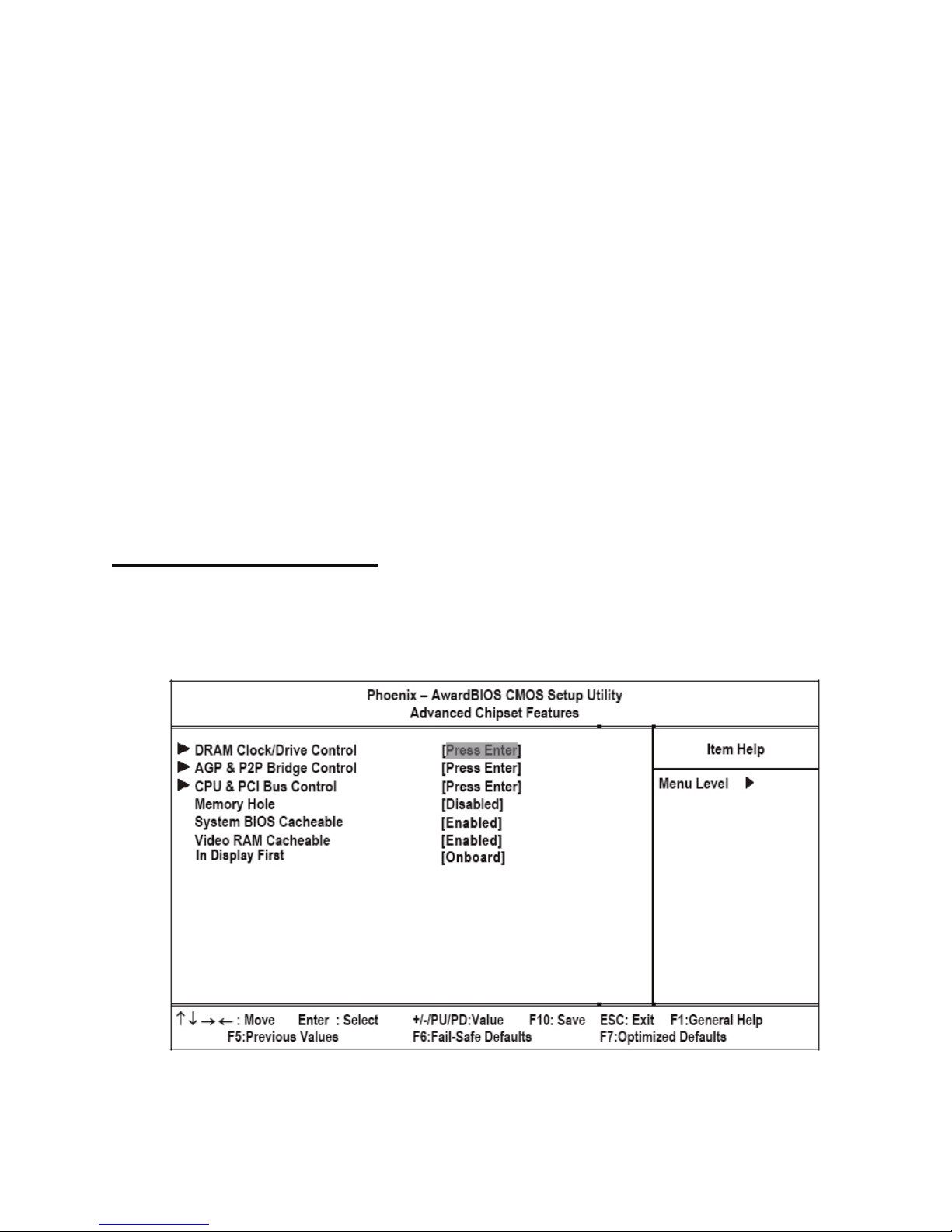
Advanced Chipset Features
This option displays critical timing parameters of the mainboard. Leave the items on this menu at their default settings
unless you are very familiar with the technical specifications of the system hardware. If you change the values incorrectly, you may introduce fatal errors or recurring instability into the system.
Figure 2.4 Advanced Chipset Features menu
Advanced BIOS Features 13
DRAM Clock/Drive Control (See “DRAM Clock/Drive Control” on page 14.)
AGP & P2P Bridge Control (See “AGP & P2P Bridge Control” on page 17.)
CPU & PCI Bus Control (See “CPU & PCI Bus Control” on page 17.)
Memory Hole
This item can be used to reserve memory space for some ISA expansion cards that require it. The default setting is Disabled.
Cacheable
These items allow the system to be cached in memory for faster execution. We recommend that you leave these items
at the default value. The default setting is Enabled.
Video RAM Cacheable
These items allow the video RAM to be cached in memory for faster execution. We recommend that you leave these
items at the default value. The default setting is Enabled.
Init Display First
Use this item to specify whether the graphics adapter is installed in one of the PCI slots or is integrated on the mainboard. The default setting is Onboard.
DRAM Clock/Drive Control
Selecting DRAM Clock/Drive Control displays this menu:
Figure 2.5 DRAM Clock/Drive Control menu
Current FSB/DRAM Frequency
Displays the current FSB and DRAM frequencies of the system. These fields are display only.
14 BIOS Setup Utility

DRAM Clock
This item enables you to manually set the DRAM Clock to 200 MHz. We recommend that you leave this item at the
default value. The default value is By SPD.
DRAM Timing
Set this to the default value to enable the system to automatically set the SDRAM timing by SPD (Serial Presence
Detect). SPD is an EEPROM chip on the DIMM module that stores information about the memory chips it contains,
including size, speed, voltage, row and column addresses, and manufacturer. The default value is By SPD.
When the DRAM Timing setting is set to “Manual” the fields that previously had an “x”
before them become available.
NOTE
SDRAM CAS Latency
This item enables you to specify the time delay (in clock cycles or CLKs) that elapses before the SDRAM carries out a
read command after receiving it. The value specified here also sets the number of CLKs that will elapse for the completion of the first part of a burst transfer. Low values indicate a faster data transaction. When synchronous DRAM is
installed, the number of clock cycles of CAS latency depends on the DRAM timing. The default is 2.5.
Bank Interleave
Enable this item to increase memory speed. When enabled, separate memory banks are set for odd and even addresses
and the next byte of memory can be accessed while the current byte is being refreshed. The default is Disabled.
Precharge to Active(Trp)
This item is used to designate the minimum Row Precharge time of the SDRAM devices on the module. DRAM must
continually be refreshed or it will lose its data. Normally, DRAM is refreshed entirely as the result of a single request.
This option allows you to determine the number of CPU clocks allocated for the Row Address Strobe (RAS) to accumulate its charge before the DRAM is refreshed. If insufficient time is allowed, refresh may be incomplete and data
lost. The default is 3T.
Active to Precharge(Tras)
This item specifies the number of clock cycles needed after a bank active command before a precharge can occur. The
default is 6T.
Active to CMD(Trcd)
This item specifies the minimum required delay between activation of different rows. The default is 3T.
REF to ACT/REF (Trfc)
Set REP to ACT / REF to 21T (Default value:21T)
Act 0 to Act 1 (TRRD)
Set ACT(0) to ACT(1) to 3T(Default value:3T)
DRAM Command Rate
This item enables you to specify the waiting time for the CPU to issue the next command after issuing the command to
the DDR memory. We recommend that you leave this item at the default value. The default value is 2T Command
RDSAIT mode
Auto: Auto detect RDSAIT mode. (Default value)
Manual: Set RDSAIT mode by manually.
Advanced BIOS Features 15

RDSAIT selection
Set RDSAIT to 03 (Default value:03)
Press <Esc> to return to the Advanced Chipset Features menu.
16 BIOS Setup Utility
AGP & P2P Bridge Control
Selecting AGP & P2P Bridge Control displays this menu:
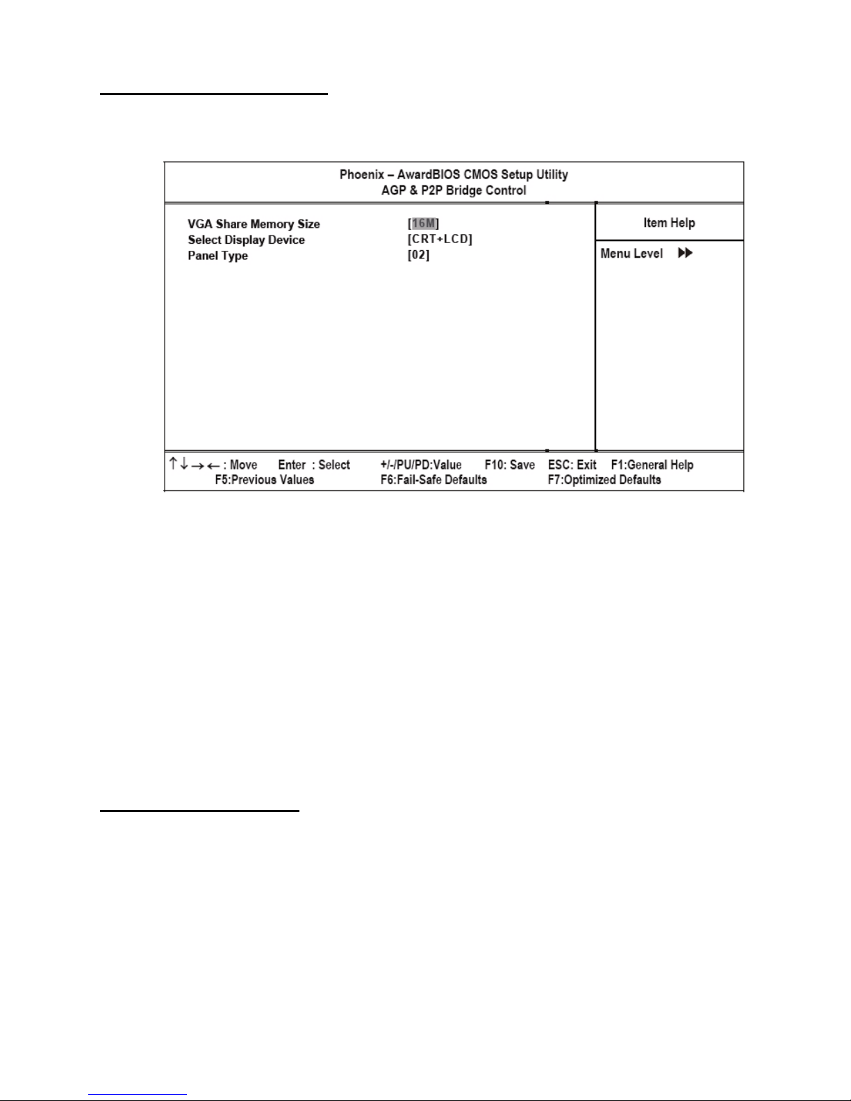
Figure 2.6 AGP & P2P Bridge Control menu
VGA Share Memory Size
The VGA is built into the chipset and is assigned 16 MB of system memory by default. Use this setting to assign additional memory to the VGA. If you have 512 MB of system memory, the maximum that you can assign to VGA is 64
MB. The default setting is 16 MB.
Select Display Device
If you connect an external display to the PT-5700, you can use this setting to turn off LCD and only use the external
display. To use dual displays this must be set to CRT+LCD. The Default setting is CRT+LCD.
Panel Type
This setting allows the mainboard to be used with different panel type. Unless you change the panel of the PT-5700,
leave this setting at its default. The default setting is 02.
CPU & PCI Bus Control
Selecting CPU & PCI Bus Control displays this menu:
Advanced BIOS Features 17
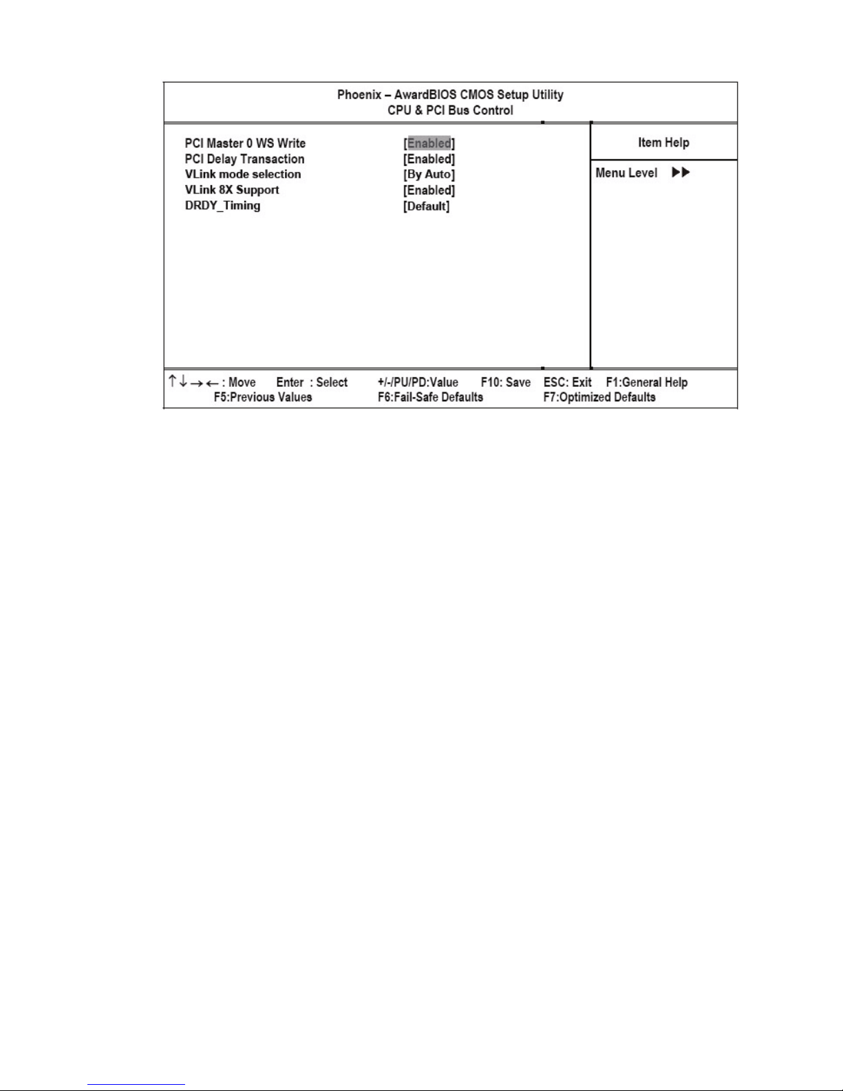
Figure 2.7 CPU & PCI Bus Control menu
PCI Master 0 WS Write
When enabled, writes to the PCI bus are executed with zero wait states. The default setting is Enabled.
PCI Delay Transaction
The mainboard’s chipset has an embedded 32-bit post write buffer to support delay transactions cycles. Select Enabled
to support compliance with PCI specification version 2.1. The default setting is Enabled.
VLink mode selection
This menu item controls the data transfer speed between the north and south bridge.
By Auto: VLink mode selection by automatically. (Default value)
Mode 0: Set VLink mode to mode 0.
Mode 1: Set VLink mode to mode 1.
VLink 8X Support
Disabled: Disabled VLink 8x support.
Enabled: Enabled VLink 8x support.(Default value)
DRDY_Timing
Default: Set default to DRDY_Timing.(Default value)
Slowest: Set slowest to DRDY_Timing.
Optimize: Set optimize to DRDY_Timing.
18 BIOS Setup Utility
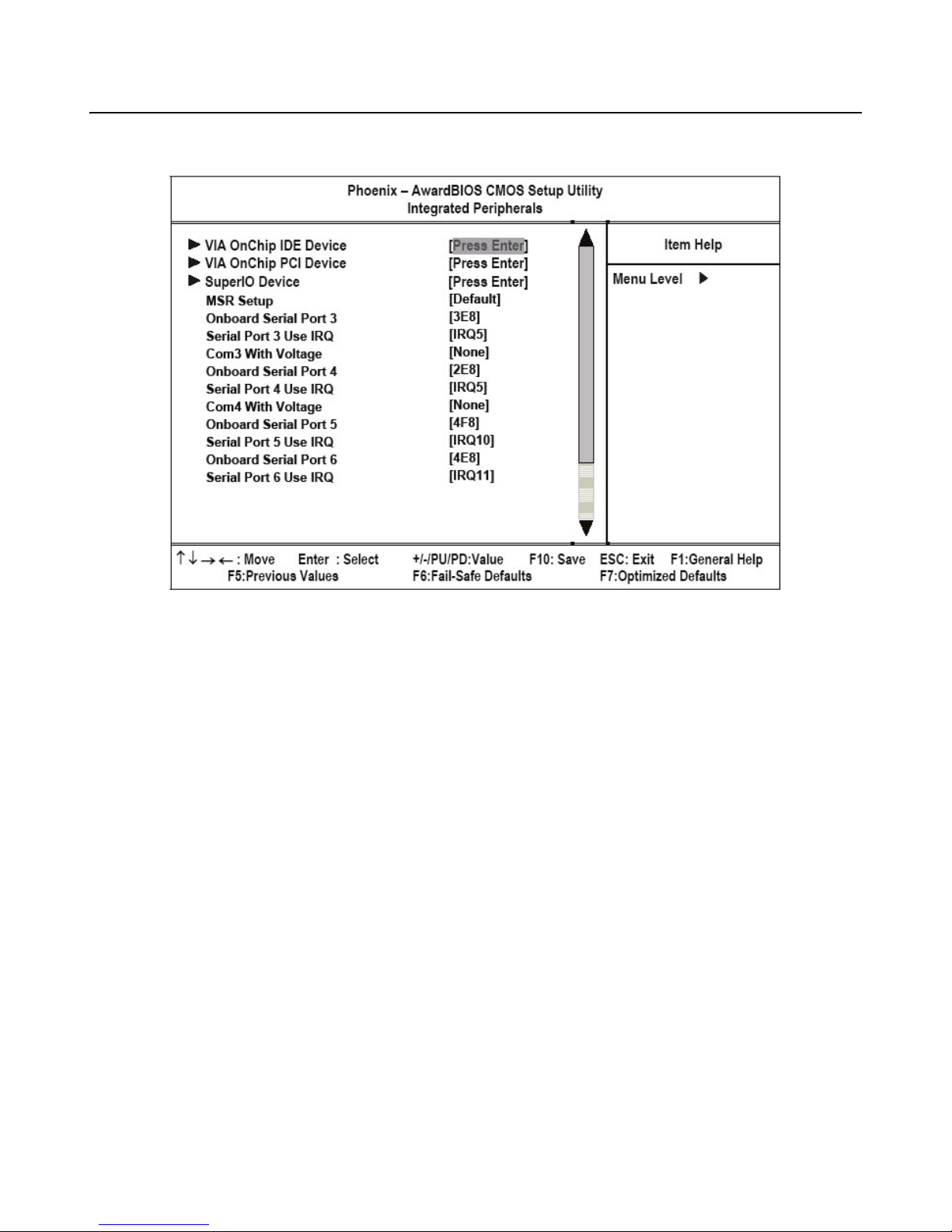
Integrated Peripherals
This option defines the operation of peripheral components on the system's input/output ports.
Figure 2.8 Integrated Peripherals menu
VIA OnChip IDE Device (See “VIA OnChip IDE Device” on page 21.)
VIA OnChip PCI Device (See “VIA OnChip PCI Device” on page 22.)
SuperIO Device (See “SuperIO Device” on page 23.)
MSR Setup
Magnetic Stripe Reader (MSR). The MSR is an industry standard keyboard wedge type MSR. This item enables you to
specify the OPOS or the standard default MSR setting.
Onboard Serial Port 3
This option is used to assign the I/O address for the onboard serial port 3 (COM3), which is used for the rear customer
display. The default setting is 3E8.
Serial Port 3 Use IRQ
This option is used to assign the interrupt request (IRQ) for the onboard serial port 3 (COM3). The default setting is
IRQ 5.
COM3 With Voltage
COM ports can be set to supply both data and power to the peripherals that connect to them. Check if the device you
connect needs power from the COM port or if it has its own power supply. The default setting for COM3 is None.
Onboard Serial Port 4
This option is used to assign the I/O address for the onboard serial port 4 (COM4). The default setting is 2E8.
Integrated Peripherals 19
 Loading...