

Page 1

COLOR TELEVISION
TC1475 / TC2175/ TF2139
TC1475 TC2175 TF2139
Page 2

TC1475 / TC2175 / TF2139 1
Contents
Contents
1. BRIEF INTRODUCTION...................................................................2
2. ELECTRICAL SPECIFICATIONS.......................................................3
3. STRUCTURE BLOCK DIAGRAM.......................................................4
4. DIAGRAM SCHEMATIC TC1475 / TC2175 .....................................6
5. DIAGRAM SCHEMATIC TF2139......................................................7
6. DIAGRAM PICTORIC TC1475 / TC2175 ..........................................8
7. DIAGRAM PICTORIC F2139 ...........................................................9
8. EXPLODED VIEW TC1475 / TC2175................................................10
9. EXPLODED VIEW TF2139...............................................................11
10. DEFINITION & FUNCTION OF TMPA8873-XXXX PINS...................12
11. REMOTE CONTROL (KEY ASSIGNMENTS LIST).............................15
12. CIRCUIT ANALYSIS.....................................................................16
13. THE T08 CHASSIS MAINLY USE THE FOLLOWING IC AND
ASSEMBLIES ..............................................................................20
14. DESCRIPTIONS FOR THE OPERATION OF FACTORY MODE............21
15. ELECTRICAL PARTS LIST TC1475 ................................................24
16. ELECTRICAL PARTS LIST TC2175.................................................25
17. ELECTRICAL PARTS LIST TF2139 ................................................26
Page 3

TC1475 / TC2175 / TF2139 2
Brief Introduction
Brief Introduction
1.
TMPA8873-XXXX is introduced in this chassis, controlled by I2C bus, implement
FS PLL tuning.
1、 FS tuning 45.75M. band adjustable
2、 Tuning in USA channel table by CATV/antenna.
3、 Auto tuning, frequency fine tuning, skip setting
4、 Color Sys: PAL-M\ PAL-N\ NTSC-M auto identified
5、 2 AV input, YUV input, AV1\AV2\DVD(YUV) input preset
6、 Switch program by numeric key directly,
7、 Picture mode: personal\dynamic\standard\soft, switched by one key
8、 Picture parameters adjustment: brightness\contrast\color\ sharpness\hue
9、 Mute control: mute when switch programs and AV
10、 Power on/off timer, program timer
11、 Auto power off 15 minutes later when no signal in TV mode
12、 special halftone menu display
13、 English\French\Spanish\Portuguese menu display
14、 8 self-detect signals generated by CPU for geometry distortion adjustment
15、 50HZ/60HZ auto identified
16、 Child lock(by press DISP button 4 seconds)
17、 AV stereo, 2 volume inner control
18、 Color and vertical position of main menu variable
19、 Factory logo setting when no signal
20、 TA1304/TA1343 tone control Plug-and-Play(25”~34”)
22、 Multifunctional RC unit(LA7461、TA9028、SC6122)may be efficiency or only
one be efficiency.
Page 4
Designs and specifications are subject to change without notice.
WARNING
The chassis in this receiver is partially hot. Use an isolation
transformer between the line cord plug and power receptacle, when
servicing this chassis. To prevent electric shock, do not remove cover.
No user-serviceable parts inside. Refer servicing to qualified service
personnel.
TC1475 / TC2175 / TF2139 3
Electrical Specifications
Electrical Specifications
2.
Model Number
RF system PAL-M/N 、NTSC-M
Video system PAL-M/N 、NTSC-M
AIR
CATV(STD)
CATV(HRC)
Receiving
channel
CATV(IRC)
Channels preset 181
Antenna input 75 Ohm Coaxial Cable
Picture tube 37cm~ 86cm(14”~ 34”) diagonal
Audio output 14” 、 21”: Maximum 2.5W× 2
25” 、 29”、34”: Maximum 5W× 2
Power source AC90V~ 260V(OR AC130~ 260V)50/60Hz
Weight(Approx) 14”(11Kg), 21”(24Kg), 25”(30Kg),29”(38Kg)
Dimensions
(W× H× D) (Approx)
14” 450(W)× 410(D)× 378(H)mm
21” 580(W)× 515(D)× 520(H)mm
25” 750(W)× 528(D)× 560(H)mm
29” 840(W)× 570(D)× 650(H)mm
Power Consumption 14”=65W 21”=75W 25”=120W
29”=130W 34”=150W
Page 5
TC1475 / TC2175 / TF2139
4
Structure Block Diagram
Structure Block Diagram
3.
AV1
AV2
12871NA/2257NA
A1 A2
S-AV y
Video Audio
S Y Cb Cr
CRT
SAWF
KEY
MATRIX
RECEIVEERMP
TC4053
AV SW
FBT
T471
LA78040/TDA9302
LA78041/TDA8177
TA9028-023/022
LA7461
SC6122
EEPROM
8K bit
2 in Chip
TMPA8873-XXXX
TA1304/TA1343
TDA1030
TDA1030
Tuner
TU201
BTSC
AN5832 or
LA72700
4053
Vout
Hout
SIF
Page 6
TC1475 / TC2175 / TF2139
5
TMPA8873-XXXX Block Diagram
TMPA8873-XXXX Block Diagram
3.1.
Page 7
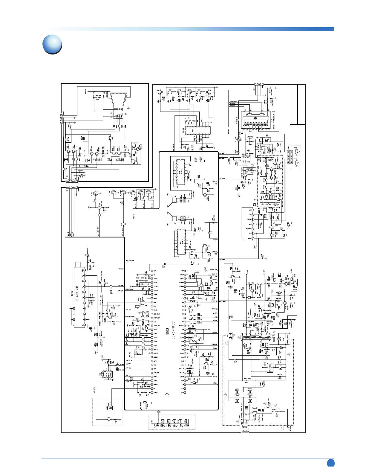
TC1475 / TC2175 / TF2139 6
Diagram Schematic TC1475 / TC 2175
Diagram Schematic
4.
*Design and specifications are subject to change without notice.
Page 8
TC1475 / TC2175 / TF2139 7
Diagram Schematic TF2139
Diagram Schematic
5.
*Design and specifications are subject to change without notice.
Page 9
TC1475 / TC2175 / TF2139
8
Diagram Pictoric TC1475, TC2175
Diagram Pictoric
6.
Page 10

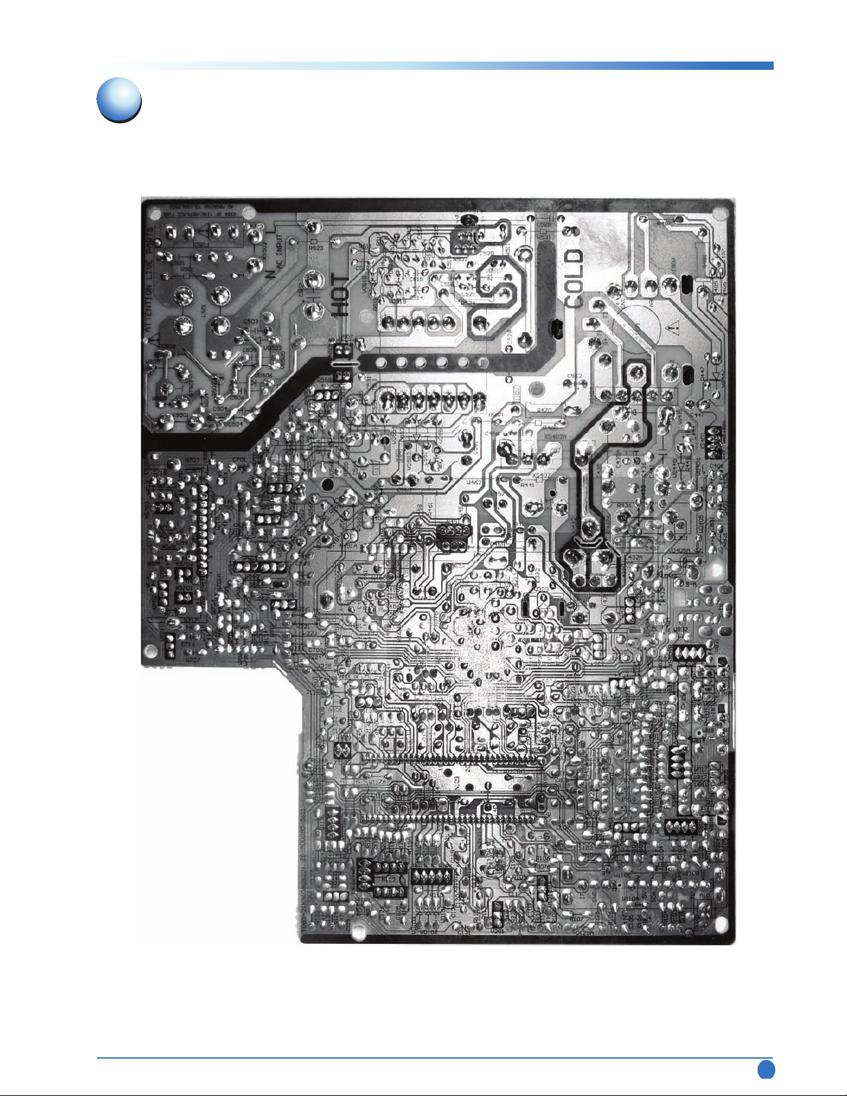
TC1475 / TC2175 / TF2139
9
Diagram Pictoric TF2139
Diagram Pictoric
7.
Page 11

TC1475 / TC2175 / TF2139
10
Exploded View TC1475/TC2175
Exploded View
8.
Page 12

TC1475 / TC2175 / TF2139
11
Exploded View TF2139
Exploded View
9.
Page 13

TC1475 / TC2175 / TF2139
12
Definition & Function of TMPA8873-XXXX Pins
Definition & Function of TMPA8873-XXXX Pins
10.
CPU part
item definition description
1 DVD high level output in DVD mode
2 NO USE
3 KEY Control signal input; general
keyboard circuit auto identified
4 GND MCU GND
5 REST MCU reset when power on
6 X-TAC
7 X-TAC
Connect ports for crystal; 20PPM precision required
8 TEST For MCU experimentation, connected to GND normal
9 5V Power input for CCD amplitude restricted circuit
10 Vss GND for CCD amplitude restricted circuit
54 GND GND for surge circuit
55 5V Power for surge circuit;
Duty cycle and Ripple voltage less than 10 mV;
56 AV SW Multi-control level output 2 or 3 TV/AV mode
57 SDA SDA input
58 SOL SCL input
59 50/60HZ Low level when 50HZ
High level when 60HZ
60 NO USE
61 MUTE MUTE control
62 NO USE
63 RMT IN
RC unit signal input
64 Power
Power control; low level for initialization; related with
item ONTIME of Page F11
Note for control port output state: (in the output table below,”0”for low level, “1” for high
level)
Pin3 Description:
Voltage range for each button (middle value is suggested)
KEY Off P+ P- V+ V- MENU TV/AV POWER
Range
0V
≤ 1.16V ≤1.74V ≤ 2.45V ≤ 3.17V ≤ 3.88V ≤ 4.60V ≤ 5V
Range
5V
0≤
0.45V
≤1.02V ≤1.74V ≤ 2.45V ≤3.17V ≤ 3.88V ≤4.60V
Page 14

Pin59 50HZ/60HZ switch
Pin59 NTSC(60HZ) PAL(50HZ)
voltage 5V 0V
Pin61 Mute 1K pull up resistance
Pin64 Power
a) RC, Pin61\64 wave:
Power
Mute
Power of
f
p
ower of
f
Power on
Mute
Cold
p
ower on
Switch
p
rogra
m
TC1475 / TC2175 / TF2139 13
Definition & Function of TMPA8873-XXXX Pins
Pin6, Pin7 less than 20PPM precision required for crystal
Duty cycle and Ripple voltage of power for Pin55 must less than 10 mV;
power for OSD clock)
Pin56 AV/TV switch
TV
AV1/S/DVD AV2
Connect way
OPT.2=0
0V
0V
5V
Pull up resistance
connected to 5V
or 8V
OPT.2=1;OPT.5=0
0V
2.5V
5V
10K pull up
esistance connected
to 5V and 10K pull
down resistance
connected to GND
0V
5V
2.5V
10K pull up
resistance
connected to 5V
OPT.2=1;OPT.5=1
Page 15

Mute setting
0
Not mute in no signal TV mode
when no blue background,
MODE2.0
1
Mute in no signal TV mode
when no blue background
0
Mute in no signal AV mode
when no blue background
MODE2.1
1
Not mute in no signal AV mode
when no blue background
Signal transacting part:
TC1475 / TC2175 / TF2139
14
Definition & Function of TMPA8873-XXXX Pins
Analog GND
Input port for flyback pulse
Output port for horizontal driver pulse
Connect port for horizontal AFC filter
The voltage of this port control the frequency of H-VCO
Connect capacitor for SAW generating,
The amplitude of SAW is a constant because of the
controlling of V-AGC
Vertical driver pulse output
8V power for deflection
Analog GND
Input port for Cb signal
Input port for Y signal
Input port for Cr signal
AUDEO1 input
Input port for C signal
Input port for CVBS/Y signal
Interface for ACL filter
Input port for TV video signal
ABCL input
Port 1 for audio output with volume control function
Port 2 for audio output with volume control function
PIF demodulation signal(full TV signal) output
Sound intermediate frequency output(may no periphery
circuit)
AUDEO2 input
Second sound intermediate frequency or horizontal phase
emendation signal input
Connect with capacitor
TV GND
FBP-IN
H-out
H-AFC
V-SAW
V-out
H-Vcc
TV GND
Cb
Y-IN
Cr
EXT-AU1
C-in
V2
ACL
TV-in
ABC-in
Audio-out1
Audio-out2
TV-out
SIF
EXT-AU2
SIF in
DC NF
11
12
13
14
15
16
17
18
19
20
21
22
23
24
25
26
27
28
29
30
31
32
33
34
Page 16

35
PIF•PLL
36 IF-5V
37 S-Reg
38 AU OUT
39 IF AGC
40 IF GND
41 IF in
42 IF in
43 RF AGC
44 Black Det
45 Monitor out
46 APC fil
47 YC VCC5V1
48 SYNC OUT
49
DVCC
3.3V
50 R out
51 G out
52 B out
53 GND
TC1475 / TC2175 / TF2139
15
Remote control (key assignments list)
11.
Remote control (key assignments list)
Connect with PIF-PLL filter
5V power for IF
Connected with filter capacitor, stabilization inner bias
Audio output, not with volume control
Connected with AGC filter
IF GND
Pin41、Pin42 are input port for differential amplifier,
input IF signal from SAW
RF-AGC signal output for tuner
Connected with black detect filter
CVBS/SVM output, CVBS/SVM selected by I²C
Connected with APC filter of chroma decode circuit
Power for YC
SYNC output
Power for digital circuit
R output
G output
B output
Connected with analog GND
ico
1
2
3
4
5
6
7
8
9
0
-/--
POWER
BTSC
P.P
TV/AV
P-
function
Number key
Standby key
BTSC key
Picture mode key
TV/AV key
Channel lessen key
data
(D7-D0)
00000000
00000001
00000010
00000011
00000100
00000101
00000110
00000111
00001000
00001001
00001010
00001011
00001100
00001110
00001111
00010000
9028-0E0E
H E X
00
01
02
03
04
05
06
07
08
09
0A
0B
0C
0E
0F
10
LC6122
BF40
00
01
02
03
04
05
06
07
08
09
0A
0B
0C
0E
0F
10
7461-54H7
H E X
1
2
3
4
5
6
7
8
9
0
0a
0x12
0x1f
0x19
0x0B
0x17
7461-55K2
H E X
1
2
3
4
5
6
7
8
9
0
0a
0x1C
0x0d
0x13
0x0f
0x1a
Page 17

TC1475 / TC2175 / TF2139 16
Circuit Analysis
12.
Circuit Analysis
P+
Vol-
Vol+
MUTE
SLEEP
DISP/LOCK
RECALL
MENU
PIC
SOUND-MODE
D-MODE
Channel add key
Volume lessen key
Volume add kye
Mute key
Sleep key
Display/lock key
RECALL key
Menu key
Picture menu key
SOUND-MODE key
Factory key
00010001
00010010
00010011
00010100
00010101
00010110
00010111
00011100
0001101
00011110
00101100
11
12
13
14
15
16
17
1C
1D
1E
2C
11
12
13
14
15
16
17
1C
1D
1E
2C
0x13
0x14
0x10
0x16
0x0f
0x1b
0x1a
0x0e
0x1c
0x1d
0x11
0x1b
0x1e
0x1f
0x15
0x19
0x14
0x0e
0x10
0x0c
0b
0x1d
12.1.Tuning circuit:
Buildup by frequency synthesized, PLL tuning, controlled by I2C bus tuner
and some individual components. Tuning process controlled by correlation
pins of UOC TMPA8873-XXXX. Pin57 & pin58 of CPU output I2C tuning
data for SCL & SDA of tuner.
FS tuner introduced in this chassis, cooperate with SCL & SDA data from
pin57 & pin58 of N101, processing FS auto tuning. 33V for tuner supplied
by 110V(130V), divided by R518 and stabilized voltage by N505.
Frequency synthesized fashion is also called PLL frequency synthesized
fashion. It is the CPU controlled by channel subscribe program、band
switch and data from RC receiver and give the band switch signal. CPU set
frequency divide ratio for variable frequency divider of PLL. Variable
frequency divider dividing the local oscillation frequency from tuner and
compare the phase with benchmark frequency, adjust local oscillation
frequency accord with the local oscillation frequency needed by each channel.
12.2.Picture IF circuit:
The IF signal from tuner enter into SAW filter Z101(F45C) after amplified by
Pre-Amp built up by V103 and so forth, filtered accordance with IF characteristic and enter TMPA8873-XXXX and output PIF demodulation
signal(CVBS) from pin30, pass through the emitter follower buildup by R155
、R156、V104、R158, coupled to pin26 (inner switch)of TMPA8873-
XXXX by C147.
Page 18

TC1475 / TC2175 / TF2139
17
Circuit Analysis
12.3. Sound processing:
The SIF2, come from inner phase lock demodulate of TMPA8873-XXXX,
turned into audio signal after limiting amplifier and frequency discriminator.
Two audio signal, out of pin28 & pin29 of TMPA8873-XXXX, enter pin9 of
N681 & N691 separated and audio power amplified. They are used to driver
speakers separated after output from pin16 of N681 & N691.
12.4.Periphery AV input processing:
Periphery AV1(V1、L1、R1)input from pin5、pin 12、pin 2 of N801(
TC4053)separated. Periphery AV2(V2、L2、R2)input from pin3、pin
13、pin1 of N801(TC4053)separated. The level output from pin56 of
N103 control the switch of N801. The video signal, output from pin4 of
N801, transmitted to inner of TMPA8873-XXXX by pin24 of N103 after switched. The audio signal, output from pin14 & pin15 of N801, transmitted to
inner of TMPA8873-XXXX by pin24 of N103.
12. 5.Line scan:
Inner synchronize separate included in TMPA8873-XXXX, build up by VCO
surge circuit, line frequency divider, AFC circuit, line output driver. Line
driver signal output from pin13 of TMPA8873-XXX, amplified by V431
(2SC2383) at line-excited level and then amplified by V432 at line output
level.
T471 is the FBT. Volts d.c. +110V(21”)+135V(29”)enter it through
pin4. Line flyback pulse divided into two routes: one for heater (virtual value
6.3V) and one for FBP of AFC after through R405 and stabilized voltage by
VD408 (9.1V). Pulse output from pin10 of T471 rectified by VD447 and filter
by C447 and we get +180V for Pre-Amp as power supply. Pin9 of FBT is
ABL , used as input of pin27 of TMPA8873-XXXX.
12.6. Field scan:
Field output level buildup by CD78040/LA78041(N451) and its periphery
components.
Field synchronization signal enter into saw wave produce circuit after
synchronization separate. Pin16 of TMPA8873-XXXX output field saw wave
driver signal to pin1 of CD78040/LA78041by pass R451, and it is output
from pin5 after driver amplified and output power amplified at the inner of
CD78040/LA78041(N451). C450、R454、R453、R461A/B are field
feedback components for improving filed linearity and stabilizing the field
Page 19

TC1475 / TC2175 / TF2139
18
Circuit Analysis
work point. Field feedback signal enter pin7 of LA7841. VD451、C451
buildup a bootstrap rise voltage circuit. The power supply for pin6 of LA7841
is 26V during scan time and bootstrap rise voltage to 48V during flyback
time. In this way, the work efficiency of field output level is improved and
also the voltage of power supply for pin7 will not less than the pulse amplitude of pin5 during flyback, and eliminate retrace efficiency accordingly. By
the way, if the linearity of scan is not well, it is something wrong with bootstrap rise voltage circuit commonly.
12.7. H-PARAB emendation circuit:
The principle of H-PARAB emendation is to using field parabolical wave to
modulating amplitude of horizontal scan current. The current accretion
according to parabolical wave rule during electron beam scan the middle of
screen and so on the H-PARAB raster turned into rectangle raster.
12.8. Color driver:
Tricolor signal amplified by tricolor driver. The white balance adjustment of
this chassis completed under the control of I2C bus.
12.9. Power supply:
1、A3 power supply: The power supply of this chassis adopt self-excitation
pulse transformer coupling switch power. It’s very steady because of the
photo-electricity transfer component adopted for stabilized voltage sam-
pling.
1)Power supply analyses:
A.Rectifying:
A.C. 220V is delivered to bridge rectifier circuit buildup by VD503~VD506
after filted by noise filter composed by L501、R501、C501、C502, and
transformed to 300V D.D. voltage after filted by L502、C507 and powe-
red supply for collector of V513 by elementary coil of switch mode trans-
former T511.
B、Oscillator circuit:
Self-excitation oscillator circuit buildup by switch transistor V513 and
switch-mode transformer T511, and the error sampling circuit buildup by
R552~R554、RP551、VD560、V533、N501.
C.Stabilized voltage:
Photo coupler N501 buildup by a LED and a photo trail-transistor. The
work state of photo trail-transistor controlled by the light emitted by LED.
Page 20

TC1475 / TC2175 / TF2139
19
Circuit Analysis
The voltage controlling LED get from 110V/130V by sampling circuit
buildup by R552~R554、RP551、VD560、V553. The voltage from
collector of V553, connected with the LED negative inner
N501,controlling the light emitted by LED.
D.Rectifier and Filter Circuit:
Switch-mode transformer T511 supply different working voltage for
chassis by its 4 secondary windings and separate the power supply of
chassis from mains supply..
2、WIDE POWER(90V~260V)IC-W65XX Introduction:
A、W65XX Block diagram(Connection diagram):
Page 21

B Functions of Each Terminal
TC1475 / TC2175 / TF2139 20
The T08 chassis mainly use the following IC and assemblies
TMPA8873-XXXX
13.
1.14~21”(AC90~260V)
2、25~34”(AC90~260V)
NO.
Position
Type
Function De scription
1
N103
8873CPBNG XXX
Controller and small signal processor
2
N102
ATME24C08
EEPROM
3
N801
HM14053N
Analog swtich
4
N451
CD78040/LA78040
Vertical scan output stage circuit
5
N681、N691
TDA1030
Audio processor
6
N502
STR-W6553A
Power supply cir cuit
7
TU201
ET-5C511-M04
Tuner
NO.
Position
Type
Function Description
1
N101
8873CPBNGXXX
Controller and small signal processor
2
N102
ATME24C08
EEPROM
3
N801
HM14053N
Analog swtich
4
N451
LA78041/TDA8177
Vertical scan output stage circuit
5
N701
AN7522/AN17821
Audio Amplifier
6
N502
STR-W6556A
Power supply circuit
7
TU201
ET-5C511-M04
Tuner
8
N601
TDA1343/TDA1304
Audio Processor
Terminal
No.
Symbols
Descriptions
Functions
1
D
Drain terminal
Mosfet Drain
2
—
—
—
3
S/GND
Source and Ground terminal
MOSFET Source and Ground
4
Vcc
Power supply terminal
Input of power supply for control circuit
5
SS/ADJ
Soft-Start and Over-current protection
adjustment Terminal
Adjustment of over-current protection and Soft
Start Operation Time set up
6
FB
Feed back terminal
Constant Voltage Control Signal Input and
Burst(intermittent)mode Oscillation Control
7
BD
Bottom Detection Terminal
Bottom Detection Signal Input and External
Latch Signal Input
Page 22

TC1475 / TC2175 / TF2139
21
Descriptions for the operation of factory mode
Descriptions for the operation of factory mode
14.
14.1. How to enter the factory mode:
A、Use remote control:
Press panel Volume down (V-) key of the TV set to lower the volume to
0(don't release it) while pressing the display key of the remote unit to enter
debug menu of factory mode 。
B、Use factory remote control:
Press“FAC”key, goes to the debug menu of factory mode directly
2)How to exit from factory mode
A、Use remote control:
1)Press ”DISP” key, then TV system will exit from the factory debug
menu status to normal status
2)Switch off the power supply and power on, then TV system will exit
from the factory mode and goes to normal status
B、Use factory remote control:
Press FAC” key, then TV system will exit from the factory debug menu
status to the factory aging mode, Press “FAC” key again, system will go
to normal status.
14.2.Direct key function descriptions for factory mode, In factory mode,
some keys function will be changed to factory function key for
debugging.
1) Mute Key: Page Up for factory mode menu
Return Key: Page Down for factory mode menu
“CH+、CH-” Key: Select the item of menu
“VOL+、VOL-” Key: Modify the data
2) Press “-/--” Key,V Stop function will implement and shows a horizontal
line for the white balance adjustment.
“1” Key R-CUT increase
“4” Key R-CUT decrease
“2” Key G-CUT increase
“5” Key G-CUT decrease
“3” Key B-CUT increase
“6” Key B-CUT decrease
4)Press“DISP”key, 4 kind of test signal will be displayed on the screen.
Page 23

TC1475 / TC2175 / TF2139
22
Descriptions for the operation of factory mode
14.3. Items on page F0~F5:
F 0:NTSC Geometr adjust(not for PAL
F 1:PAL Geometr adjust(offset refer to NTSC)only for PAL signal
F 2:Broghtness balance adjust
Items
Description
Recommend Data
Max
NT.H.PHASE
Horizontal Phase for 60Hz system
19
31
NT.V.POSI
Vertical Phase for 60Hz system
01
15
NT.V.SISE
Vertical Amplitude for 60Hz system
28
63
NT.V.LIN
Vertical Linearity for 60Hz system
15
31
NT.V.SC
V-S correction for 60Hz system
15
31
NT.HBOW
H Bow correct for 60Hz system
04
07
NT.HPARA
Parallelogram correct for 60Hz system
04
07
H.BLK.LEFT
Horizontal Left vanish
0
07
H.BLK.RIGHT
Horizontal Right vanish
0
07
Items
Description
Recommend Data
Max
H.PHASE
Horizontal Phase for 50Hz system
0
-11~10
V.POSITION
Vertical Phase for 50Hz system
0
-11~10
V.SIZE
Vertical Amplitude for 50Hz system
0
-11~10
V.LIN
Vertical Linearity for 50Hz system
0
-11~10
V.SC
V-S correction for 50Hz system
0
-11~10
HBOW
H Bow correct for 50Hz system
4
-8~07
HPARA
Parallelogram correct for 50Hz system
4
-8~07
Items
Description
Recommend Data
Max
RC
Red cut
32
255
GC
Green cut
32
255
BC
Blue cut
32
255
GD
Green driver
60
127
Blue driver
72
127
SB
Sub Brightness
00
63
Page 24

TC1475 / TC2175 / TF2139 23
Descriptions for the operation of factory mode
Items
Description
Recommend Data
Max
SUB.CONT
Sub-contrast
12
15
SUB.COLOR
Sub-color
10
127
ST3
TV NTSC3.58 high frequency advance degree
37
63
SV3
AV NTSC3.58 high frequency advance degree
37
63
ST4
TV PAL4.43 high frequency advance degree
37
63
SV4
Other AV system high frequency advance degree
37
63
SVD
DVD high frequency advance degree
37
63
OSD.CONT
OSD contrast
1
15
OSD.H.POSI
OSD horizontal position
16
127
OSD.V.POSI
OSD vertical position
32
127
F3:Sub-Contrast 、Sub-Color and OSD adjustment
F4: Language adjustment
F5:AGC、Tuner BAND adjustment
Items
Description
Recommend Data
Max
ENGLISH
ENGLISH
01
01
FRENCH
FRENCH
01
01
SPANISH
SPANISH
01
01
PORTUGUESE
PORTUGUESE
00
01
Items
Description
Recommend Data
Max
RF.AGC
Automatic gain control
35
63
MENU1
Color option for tool bar of menu
13
15
MENU2
Translucence color option of mene
8
15
VHL
VHL BAND
39
79
UHF
UHF BAND
127
127
POWER
0:Standby;1:open;2:menory
2
2
PAGE
Sub –menu of factory mode
00
01
Page 25

TC1475 / TC2175 / TF2139 24
Electrical Parts List TC1475
15.
Electrical Parts List
05-8873CS-C10
CPU
INTEGRATED
CIRCUIT
CONTROL
IC 8873CSCNG6UP3
34-457FF5-N01-2
TUNER
TUNER
ET-5C511-M04
19-F00010-000-D
FBT
HIGH VOLTAGE
FLY-BACK
TRANSFORMER
FBT
BSC24-01N4010GV
03-0W6553-AA0
POWER IC
PWM
REGULATOR
POWER IC
STR-W6553A
03-SD1555-0A0
HORIZONTAL
OUTPUT
TRANSISTOR
HORIZONTAL
TRANSISTOR
2SD1555
05-T24C08-U10
MEMORY IC
MEMORY IC
08B(AT24C08B-PU)
40-03150D-1GT-6
FUSE Fuse T3.15AL250VAC
SPEAKER 8 OHM / 5W
81-09016W-213
REMOTE
CONTROL
RS09 REMOTE
CONTROL MTI
8891-1002 (Parker)
8873-6UP3
TC1475-14E2A
CHASSIS
PCB MAIN
Chassis Parker
TC1475
8873-6UP3
TC1475
MODEL
PART NUMBER
DESCRIPTION
SPECIFICATION
PHOTO
81-09016W-000
Page 26

TC1475 / TC2175 / TF2139
25
Electrical Parts List TC2175
16.
Electrical Parts List
05-8873CS-C10
CPU
INTEGRATED
CIRCUIT
CONTROL
IC 8873CSCNG6UP3
34-457FF5-N01-2
TUNER
TUNER
ET-5C511-M04
19-F00080-000-D
FBT
HIGH VOLTAGE
FLY-BACK
TRANSFORMER
FBT
BSC24-01N4006EV
03-0W6553-AA0
POWER IC
PWM
REGULATOR
POWER IC
STR-W6553A
03-SD1555-0A0
HORIZONTAL
OUTPUT
TRANSISTOR
HORIZONTAL
TRANSISTOR
2SD1555
05-T24C08-U10
MEMORY IC
MEMORY IC
08B(AT24C08B-PU)
40-03150D-1GT-6
FUSE Fuse T3.15AL250VAC
SPEAKER 8 OHM / 5W
81-09016W-213
REMOTE
CONTROL
RS09 REMOTE
CONTROL MTI
8891-1002 (Parker)
8873-6UP3
TC2175-21E2A
CHASSIS
PCB MAIN
Chassis Parker
TC2175
8873-6UP3
TC2175
MODEL
PART NUMBER
DESCRIPTION
SPECIFICATION
PHOTO
81-09016W-000
Page 27

TC1475 / TC2175 / TF2139
26
Electrical Parts List TF2139
17.
Electrical Parts List
05-8873CS-C10
CPU
INTEGRATED
CIRCUIT
CONTROL
IC 8873CSCNG6UP3
34-457FF5-N01-2
TUNER
TUNER
ET-5C511-M04
19-F00080-000-D
FBT
HIGH VOLTAGE
FLY-BACK
TRANSFORMER
FBT
BSC24-01N4006EV
03-0W6553-AA0
POWER IC
PWM
REGULATOR
POWER IC
STR-W6553A
03-SD1555-0A0
HORIZONTAL
OUTPUT
TRANSISTOR
HORIZONTAL
TRANSISTOR
2SD1555
05-T24C08-U10
MEMORY IC
MEMORY IC
08B(AT24C08B-PU)
40-03150D-1GT-6
FUSE Fuse T3.15AL250VAC
SPEAKER 8 OHM / 5W
81-09016W-213
REMOTE
CONTROL
RS09 REMOTE
CONTROL MTI
8891-1002 (Parker)
8873-6UP3
TF2139-21E2A
CHASSIS
PCB MAIN
Chassis Parker
TF2139
8873-6UP3
TF2139
MODEL
PART NUMBER
DESCRIPTION
SPECIFICATION
PHOTO
81-09016W-000
Page 28

 Loading...