

Page 1
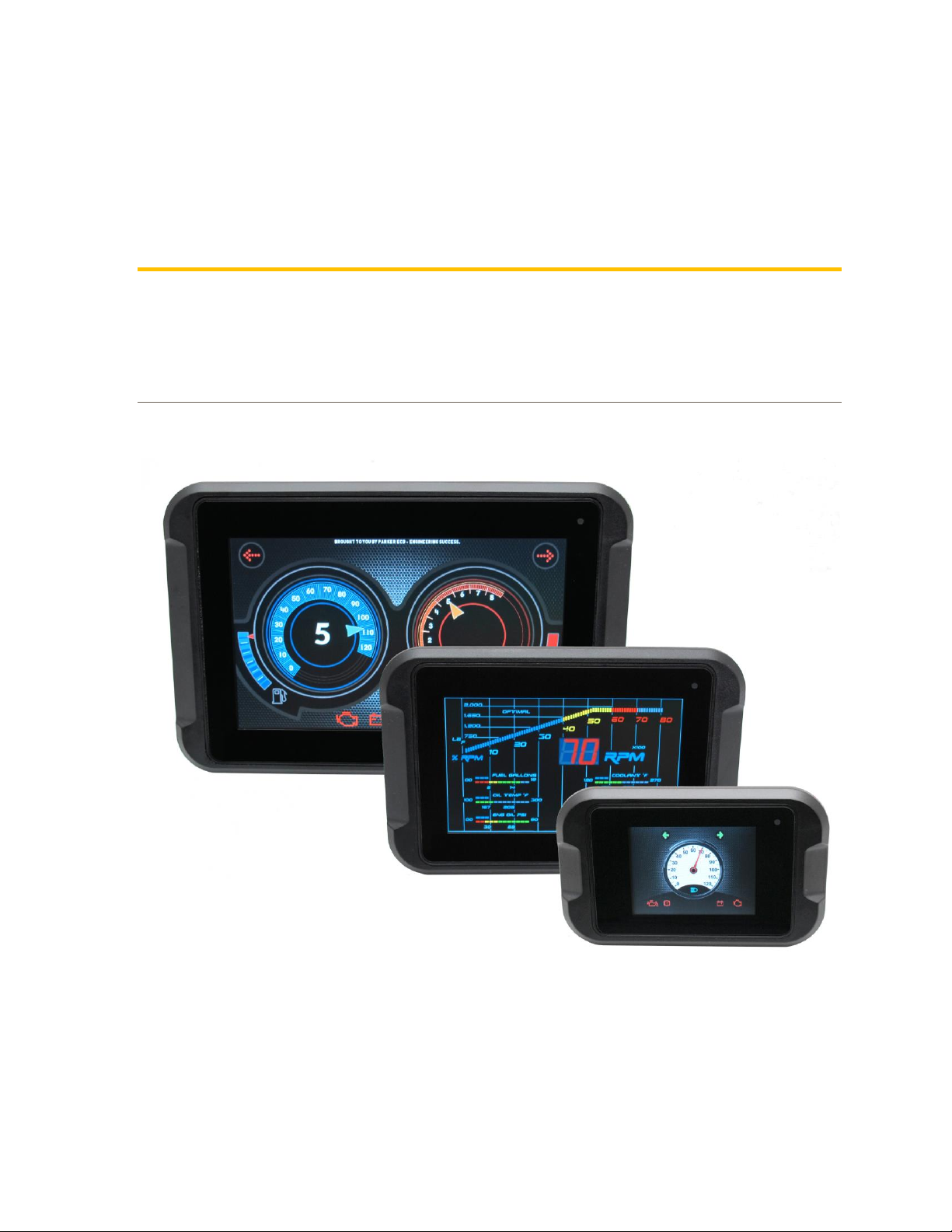
Parker Hannifin Display
PHD
User Guide
UG-PHD-1040001-201907-018
Page 2

Parker Hannifin Canada
Electronic Controls Division
1305 Clarence Avenue
Winnipeg, MB R3T 1T4 Canada
office +1 204 452 6776
Fax +1 204 478 1749
http://www.parker.com/ecd
Copyright 2019 © Parker Hannifin Corporation. All rights reserved. No part of this work may be
reproduced, published, or distributed in any form or by any means (electronically, mechanically,
photocopying, recording, or otherwise), or stored in a database retrieval system, without the prior
written permission of Parker Hannifin Corporation in each instance.
Warning!
FAILURE OR IMPROPER SELECTION OR IMPROPER USE OF THE PRODUCTS AND/OR SYSTEMS
DESCRIBED HEREIN OR RELATED ITEMS CAN CAUSE DEATH, PERSONAL INJURY AND PROPERTY
DAMAGE.
• This document and other information from Parker Hannifin Corporation, its subsidiaries and authorized
distributors provide product and/or system options for further investigation by users having technical expertise.
• The user, through its own analysis and testing, is solely responsible for making the final selection of the
system and components and assuring that all performance, endurance, maintenance, safety and warning
requirements of the application are met. The user must analyze all aspects of the application, follow applicable
industry standards, and follow the information concerning the product in the current product catalog and in any
other materials provided from Parker or its subsidiaries or authorized distributors.
• To the extent that Parker or its subsidiaries or authorized distributors provide component or system options
based upon data or specifications provided by the user, the user is responsible for determining that such data
and specifications are suitable and sufficient for all applications and reasonably foreseeable uses of the
components or systems.
• The Buyer and/or end-user will be solely responsible for final disposal of all products.
Page 3

iii
Publication History ............................................................................................................... v
Safety .................................................................................................................................... vi
Safety symbols ................................................................................................................................. vi
General safety regulations ............................................................................................................... vi
Welding after installation ................................................................................................................. vii
Construction regulations ................................................................................................................. vii
Safety during installation ................................................................................................................. vii
Safety during start-up ..................................................................................................................... viii
Safety during maintenance and fault diagnosis ............................................................................. viii
1. About the PHD (Parker Hannifin Display) ....................................................................... 1
1.1. Diagram conventions ................................................................................................................ 5
2. Connectors ........................................................................................................................ 7
2.1. Pinouts ...................................................................................................................................... 8
3. Inputs ............................................................................................................................... 13
3.1. PHD28 inputs .......................................................................................................................... 13
3.2. PHD50 inputs .......................................................................................................................... 14
3.3. PHD70 inputs .......................................................................................................................... 15
3.3.1. PHD28/PHD50 analog input capabilities ................................................................... 16
3.3.2. PHD28/PHD50/PHD70 digital input capabilities ........................................................ 18
3.3.3. PHD50/PHD70 frequency input capabilities .............................................................. 20
3.4. Using inputs as low power outputs ......................................................................................... 22
3.4.1. Low power, high-side output capabilities ................................................................... 22
4. Outputs ............................................................................................................................ 24
4.1. PHD28/PHD50/PHD70 Low-side outputs ............................................................................... 24
4.1.1. Low-side output capabilities ...................................................................................... 24
4.2. Sensor and regulated supply outputs ..................................................................................... 26
4.2.1. Sensor and regulated supply capabilities .................................................................. 27
5. Power ............................................................................................................................... 28
6. Communication ............................................................................................................... 29
6.1. Controller Area Network .......................................................................................................... 29
6.1.1. CAN capabilities ........................................................................................................ 29
6.1.2. PHD CAN installation connections ............................................................................ 30
Contents
Page 4

iv PHD
Contents
6.2. USB ......................................................................................................................................... 32
7. HMI (Human Machine Interface) .................................................................................... 33
7.1. Ambient light sensor ................................................................................................................ 33
7.2. Touchscreen ............................................................................................................................ 33
7.3. Keypad ..................................................................................................................................... 33
7.4. Buzzer ...................................................................................................................................... 33
7.5. Video ........................................................................................................................................ 34
7.5.1. Video Input Capabilities ............................................................................................. 34
8. Serial Ethernet Recovery Flexcan (SERF) Development Board ................................. 35
8.1. SERF overview ........................................................................................................................ 35
8.2. Available Inputs and Outputs................................................................................................... 36
8.2.1. Switches and Connectors .......................................................................................... 37
8.2.2. Jumpers...................................................................................................................... 38
8.2.3. DB9 Pinout Reference ............................................................................................... 41
9. Mounting the PHD ........................................................................................................... 42
9.1. Dimensions .............................................................................................................................. 43
9.1.1. PHD28 ........................................................................................................................ 43
9.1.2. PHD50 ........................................................................................................................ 44
9.1.3. PHD70 ........................................................................................................................ 45
10. Understanding PHD software ...................................................................................... 46
11. Environmental protection ............................................................................................ 47
EMI 47
Mechanical environment ................................................................................................................. 47
ESD 47
Climate environment ....................................................................................................................... 47
Chemical environment .................................................................................................................... 48
12. Index ............................................................................................................................... 49
Page 5

v
The following table provides an overview of the changes made to this document
over the course of its publication history.
Release Date
Description of Change
Rev. 001
First release of this document, 2/10/2016
Rev. 002
Updated per Bus. Dev. feedback, 3/3/2016
Rev. 003
Incremental updates from case 30666 reviews 4/6/2016 and
6/27/2016
Rev. 004
Edits based on case 30666 7/11/2016 review and 1042F06
specification
Rev. 005
Edits based on case 30666 9/12/2016 review
Rev. 006
Inputs, outputs and 5V / 12V power supply outputs, pin
naming changed, 1/11/2017
Rev. 007
Remove references to Advanced versions per Sales and
Marketing request. Will launch at a later date.
Rev. 008
Label pins in C2 as reserved for PHD50/PHD70
Rev. 009
Add SERF Development board section
Rev. 010
High-side/low power output and low-side output specification
update.
Rev. 011
Changed PHD70 brightness specification.
Rev. 012
Minor edit to Power section
Rev. 013
Added RS232 debugging pin names to PHD50/70 connector
C2 pin-out
Rev. 014
Minor edits to SERF board section.
Rev. 015
Minor edit to Power section.
Rev. 016
Minor edit to PHD70 feature table and Environmental
protection section, 1/29/2018
Rev. 017
Removed reference to Digital inputs from PHD28/50, added
USB file loading and Recovery switch information.
Rev. 018
Edits per Product Manager markups 3/2019 and 6/2019
Publication History
Page 6

vi
Do not perform the procedures in this manual unless you are experienced in the
handling of electronic equipment.
Contact the manufacturer if there is anything you are not sure about or if you have
any questions regarding the product and its handling or maintenance.
The term "manufacturer" refers to Parker Hannifin Corporation.
Safety symbols
The following symbols are used in this document to indicate potentially
hazardous situations:
Danger! Risk of death or injury.
Warning! Risk of damage to equipment or degradation of signal
When you see these symbols, follow the instructions carefully and proceed with
caution.
General safety regulations
Work on the hydraulics control electronics may only be carried out by trained
personnel who are well-acquainted with the control system, the machine, and its
safety regulations.
Follow the manufacturer's regulations when mounting, modifying,
repairing, and maintaining equipment. The manufacturer assumes no
responsibility for any accidents caused by incorrectly mounted or
incorrectly maintained equipment. The manufacturer assumes no
responsibility for the system being incorrectly applied, or the system
being programmed in a manner that jeopardizes safety.
Safety
Page 7

vii
Safety
Do not use the product if electronic modules, cabling, or connectors are
damaged or if the control system shows error functions.
Electronic control systems in an inappropriate installation and in
combination with strong electromagnetic interference fields can, in
extreme cases, cause an unintentional change of speed of the output
function.
Welding after installation
Complete as much as possible of the welding work on the chassis before the
installation of the system. If welding has to be done afterwards, proceed as
follows:
Do not place the welding unit cables near the electrical wires of the
control system.
1. Disconnect the electrical connections between the system and external
equipment.
2. Disconnect the negative cable from the battery.
3. Disconnect the positive cable from the battery.
4. Connect the welder's ground wire as close as possible to the place of the
welding.
Construction regulations
The vehicle must be equipped with an emergency stop which disconnects the
supply voltage to the control system's electrical units. The emergency stop must
be easily accessible to the operator. If possible, the machine must be built so that
the supply voltage to the control system's electrical units is disconnected when the
operator leaves the operator’s station.
Safety during installation
Incorrectly positioned or mounted cabling can be influenced by radio
signals, which can interfere with the functions of the system.
Page 8

viii PHD
Safety
Safety during start-up
Danger! Risk of death or injury. Do not start the machine's engine
before the control system is mounted and its electrical functions have
been verified.
Do not start the machine if anyone is near the machine.
Safety during maintenance and fault diagnosis
Before performing any work on the hydraulics control electronics, ensure that
▪ The machine cannot start moving.
▪ Functions are positioned safely.
▪ The machine is turned off.
▪ The hydraulic system is relieved from any pressure.
▪ Supply voltage to the control electronics is disconnected.
Page 9
1
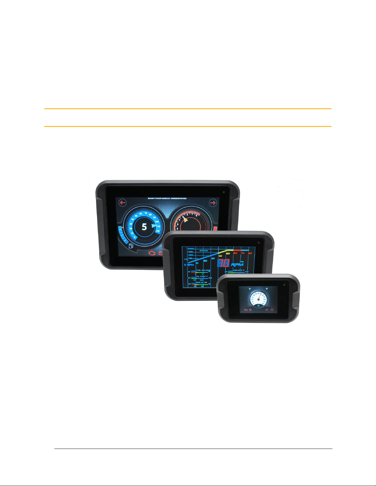
The PHD family of displays are general purpose displays suitable for a wide
range of industry applications. There are 3 sizes: 2.8", 5.0" and 7.0". All models
are color LCD displays with capacitive touchscreens for interfacing.
Figure 1: PHD family of displays
1. About the PHD (Parker Hannifin Display)
Page 10
2 PHD
About the PHD (Parker Hannifin Display)
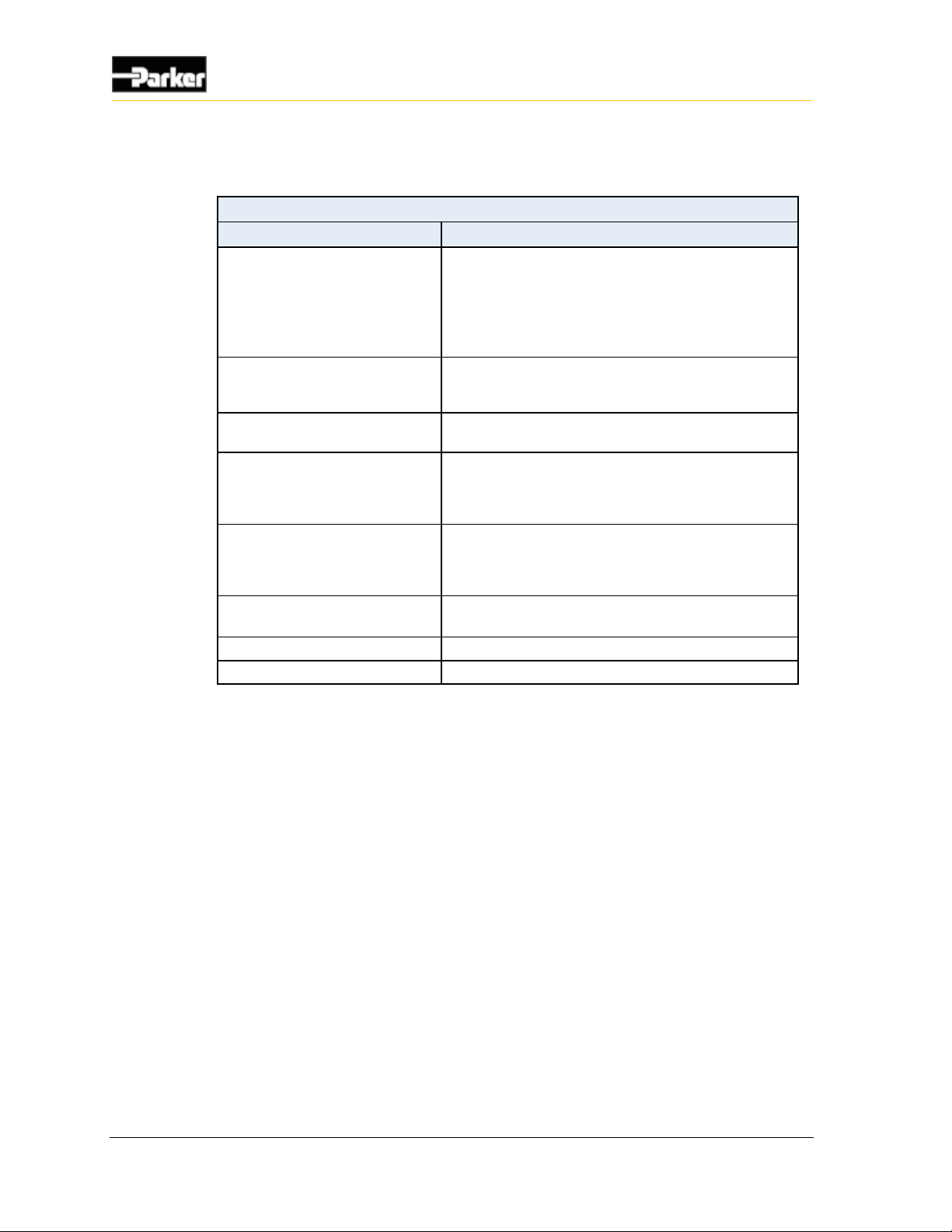
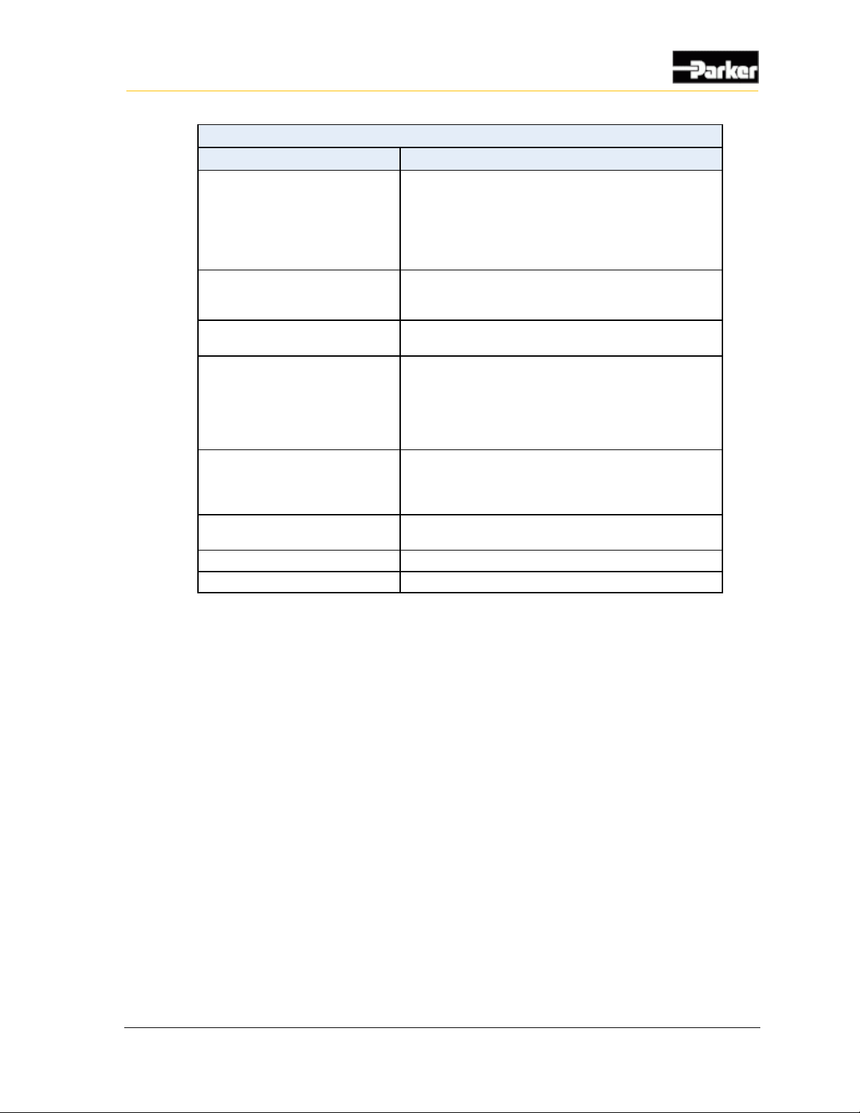
The different models of the PHD and their features are listed in the following
tables:
PHD28
Characteristic
Description
Display
Viewing angle
Brightness
Contrast ratio
Readable with polarized glasses
2.8" 320 x 240 TN LCD, PCAP touchscreen
Aspect ratio 4:3
Theta X +60° / -60°, Theta Y +60° / -50°
500 cd/m²
500:1
yes (landscape and portrait orientation)
Processor
Vybrid VF5xxR (Cortex-A5 core)
Flash 16 MB
RAM 128 MB DDR
Communication
CAN x 1
USB Host/Device x 1 (default is Device)
Inputs
7 General Purpose Inputs;
7 - Analog or
7 - GPIO used for Keypad Interface
Ambient Light Sensor
Outputs
2 x low-side 500mA
1 x 5Vdc sensor supply 500mA
1 x 12Vdc sensor supply 500mA
up to 7 high-side, 4.3V @ 5mA
Wake-up sources
Power, CAN, Touch Screen, External Keypad (GPIO)
Heater for cold applications
High wattage resistors (built-in)
Connector
Molex MX150, 20 pin
Page 11
3
About the PHD (Parker Hannifin Display)
PHD50
Characteristic
Description
Display
Viewing angle
Brightness
Contrast ratio
Readable with polarized glasses
5.0" 800 x 480 TN LCD, PCAP touchscreen
Aspect ratio 16:9
Theta X +80° / -80°, Theta Y +80° / -80°
380 cd/m²
500:1
yes (landscape and portrait orientation)
Processor
Vybrid VF5xxR (Cortex-A5 core)
Flash 32 MB
RAM 128 MB DDR
Communication
CAN x 1
USB Host/Device x 1 (default is Device)
Inputs
10 General Purpose Inputs;
2 - Frequency Inputs (for rotary encoder)
8 -Analog or
8-10 GPIO for Keypad Interface
Ambient Light Sensor
1 Video inputs (NTSC, PAL)
Outputs
2 x low-side 500mA
1 x 5Vdc sensor supply 500mA
1 x 12Vdc sensor supply 500mA
up to 10 high-side, 4.3V @ 5mA
Wake-up sources
Power, CAN, Touch Screen, External Keypad (GPIO),
Encoder
Heater for cold applications
High wattage resistors (built-in)
Connector
2 x Molex MX150, 20 pin
Page 12
4 PHD
About the PHD (Parker Hannifin Display)
PHD70
Characteristic
Description
Display
Viewing angle
Brightness
Contrast ratio
Readable with polarized glasses
7.0" 800 x 480 IPS LCD, PCAP touchscreen
Aspect ratio 16:9
Theta X +80° / -80°, Theta Y +80° / -80°
430 cd/m²
600:1
yes (landscape and portrait orientation)
Processor
Freescale iMX6Solo/Dual/Quad
Flash 1 GB
RAM 512 MB DDR3
Communication
CAN x 2
USB Host/Device x 1 (default is Device)
Inputs
10 General Purpose Inputs;
2 - Frequency Inputs (for rotary encoder)
8 - Digital (active-high/low) or
8-10 GPIO for Keypad Interface
Ambient Light Sensor
2 simultaneous Video Inputs (NTSC, PAL)
Outputs
2 x low-side 500mA
1 x 5Vdc sensor supply 500mA
1 x 12Vdc sensor supply 500mA
up to 10 high-side, 4.3V @ 5mA
Wake-up sources
Power, CAN1, CAN2, Touch Screen, External Keypad
(GPIO), Encoder
Connector
2 x Molex MX150, 20 pin
Page 13
5
About the PHD (Parker Hannifin Display)
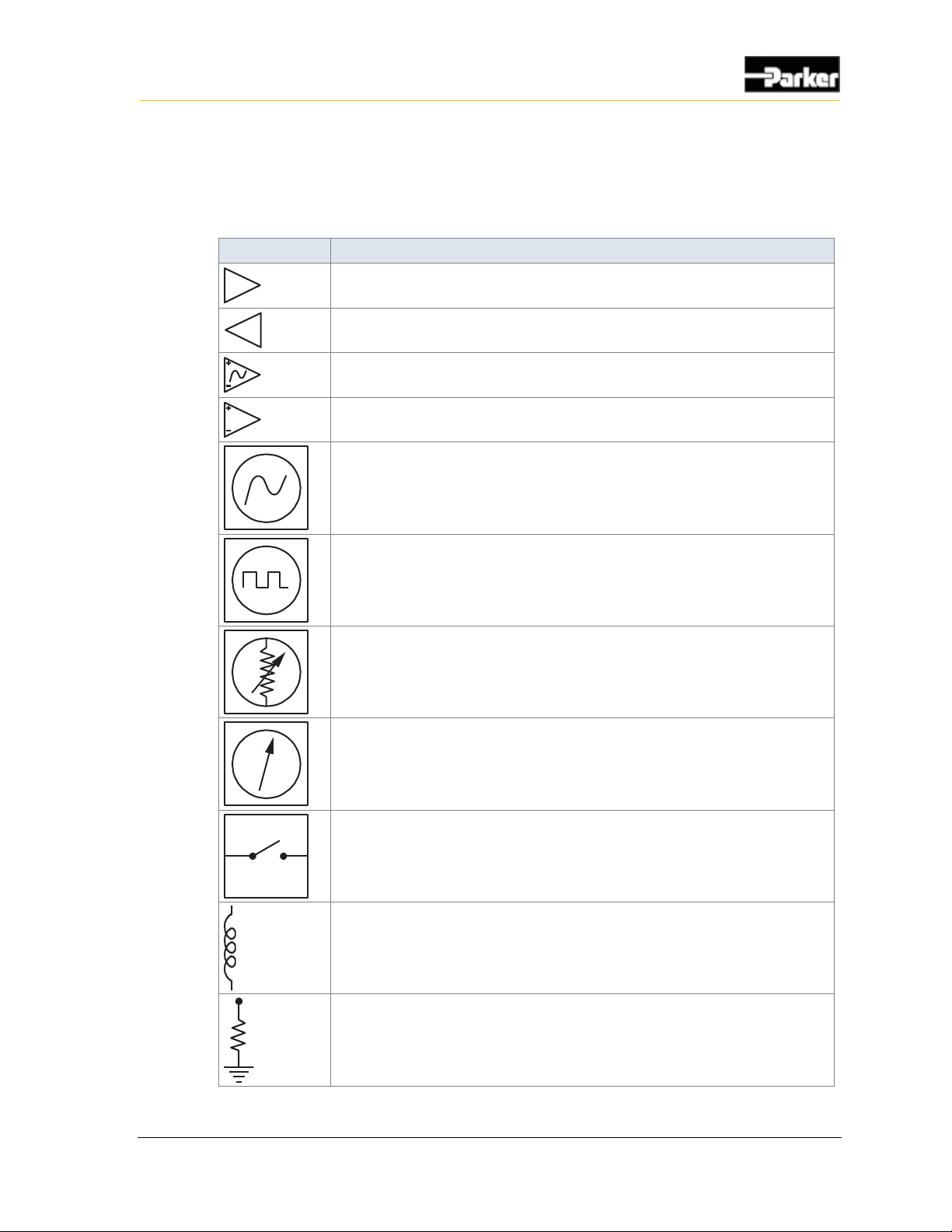
1.1. Diagram conventions
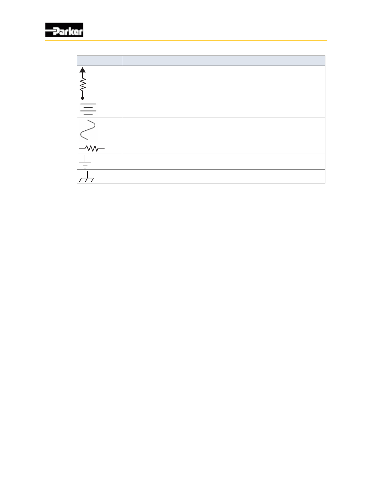
The following symbols are used in the schematic diagrams in this document:
Symbol
Meaning
General input
General output
Frequency input
Analog input
Frequency sensor
Pulse sensor
Resistive sensor
General sensor
Application switch
Load
Pull-down resistor
Page 14
6 PHD
About the PHD (Parker Hannifin Display)
Symbol
Meaning
Pull-up resistor
Battery
Fuse
Resistor
Ground
Chassis ground
Page 15
7
Connectors
The connector on the rear panel of the PHD28 is;
▪ MX150 – Vehicle Harness Connector key B
The connectors on the rear panel of the PHD50 are;
▪ 2 x MX150 – Vehicle Harness Connectors, key A & B
The connectors on the rear panel of the PHD70 are;
▪ 2 x MX150 – Vehicle Harness Connectors, key A & B
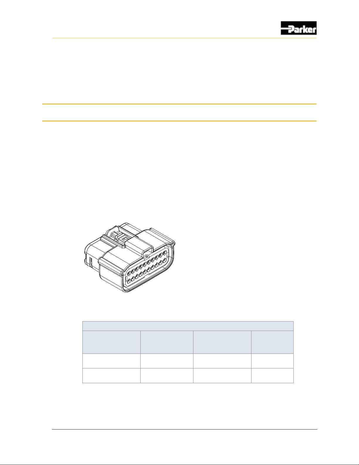
The Molex MX150 connectors are used to interface the PHD family to power,
inputs, outputs and USB.
Figure 2: MX150 20-pin connector
Mating Connector Part Numbers
PHD
Connector
Shell part no.
with locking clip
Shell part no.
without locking
clip
Terminals
J1 connector (gray),
20-pin, key option B
33472-2007
33472-2002
33001-2004
(18-20 AWG)
J2 connector (black),
20-pin, key option A
33472-2006
33472-2001
33001-2004
(18-20 AWG)
2. Connectors
Page 16
8 PHD
Connectors
2.1. Pinouts
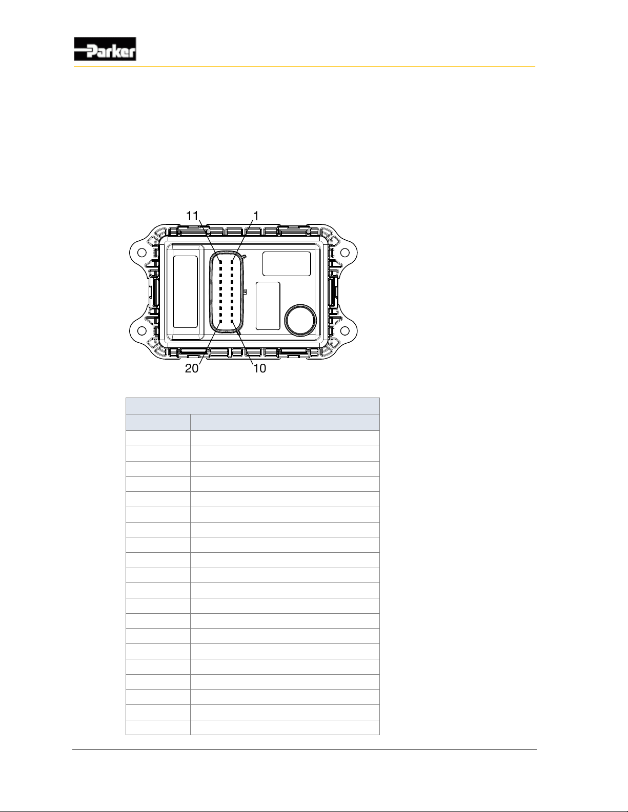
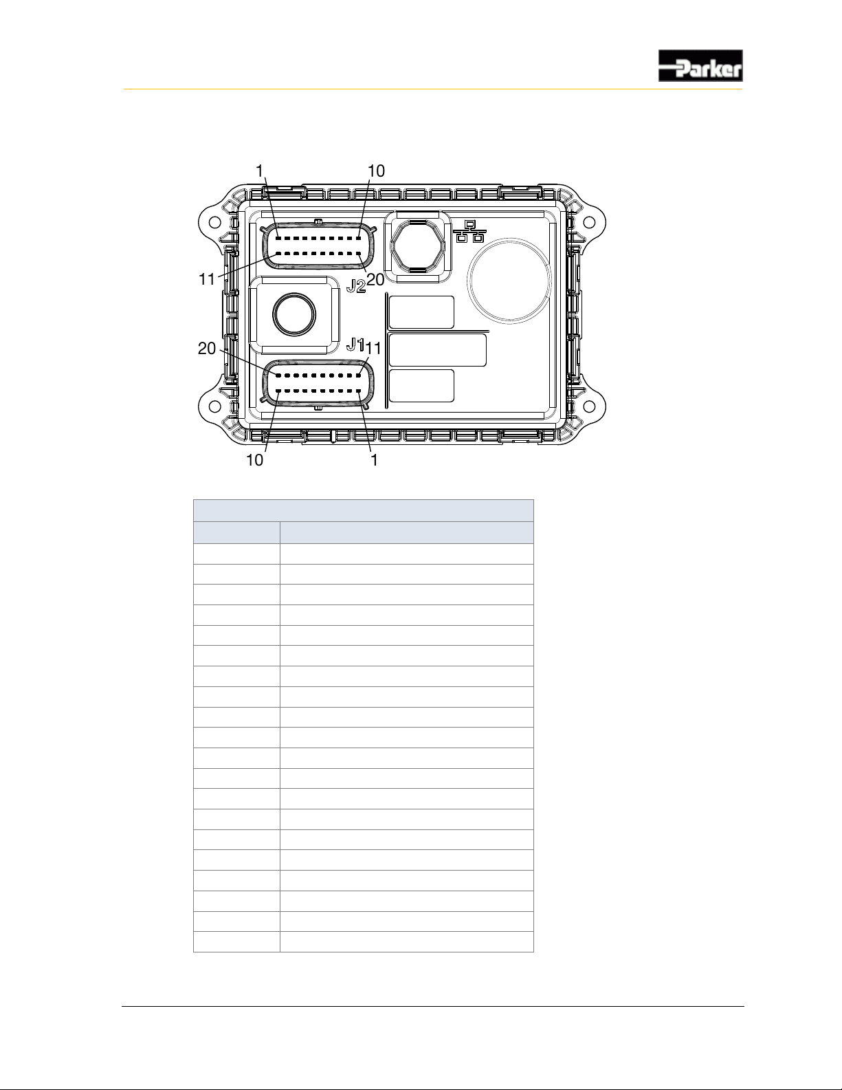
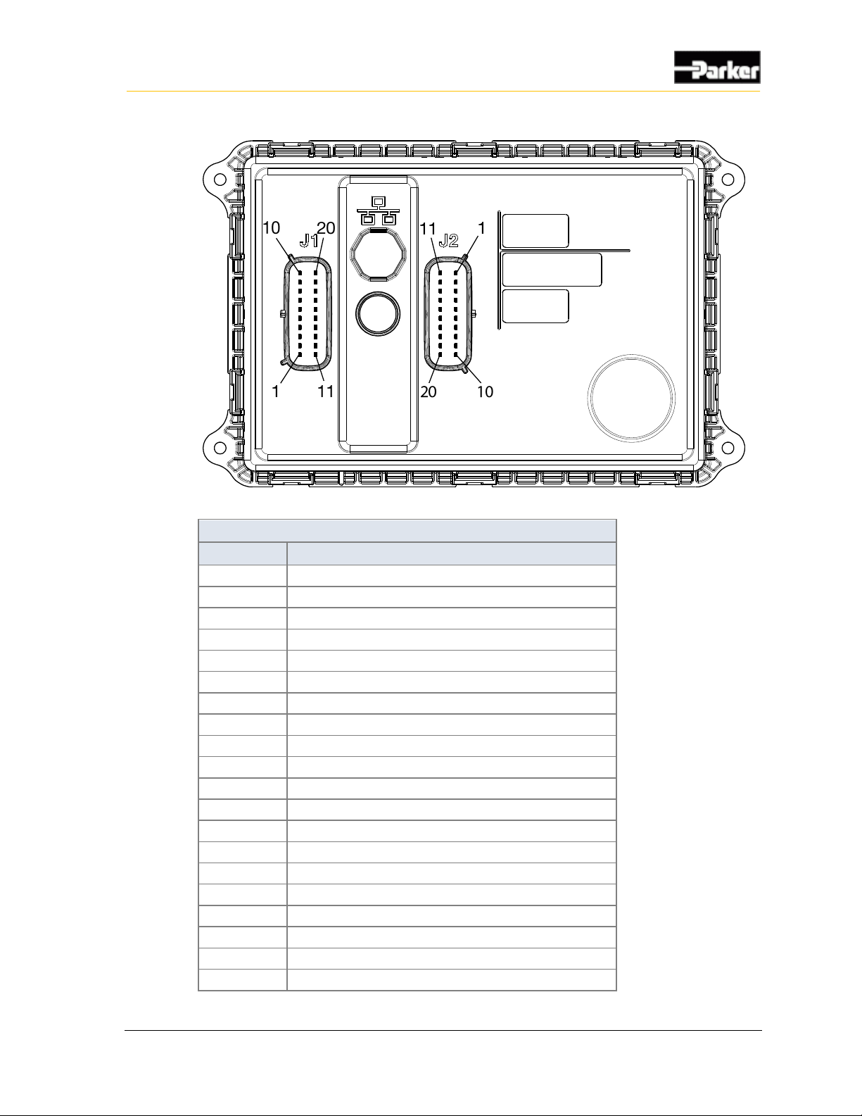
The pins in the Molex MX150 connectors connect to power, inputs, outputs, CAN
and USB communication channels.
The following tables show the pinouts for each connector:
Figure 3: Back of PHD28 showing connector
PHD28 J1 Connector Pinout
Pin
Function
1
GPIO7 (analog input/low power output)
2
GPIO1 (analog input/low power output)
3
GPIO6 (analog input/low power output)
4
OUTPUT2 (low-side output)
5
CAN1_TERM (CAN termination)
6
CAN1_SHLD (CAN shield)
7
CAN1_L (CAN low)
8
CAN1_H (CAN high)
9
GND (Negative battery)
10
+VBATT (Positive battery)
11
GPIO5 (analog input/low power output)
12
GPIO4 (analog input/low power output)
13
GPIO3 (analog input/low power output)
14
GPIO2 (analog input/low power output)
15
USB_D-
16
USB_D+
17
USB_GND
18
USB_VBUS / P5V0 (5V sensor supply)
19
P12V0 (12V regulated supply)
20
OUTPUT1 (low-side output)
Page 17
9
Connectors
Figure 4: Back of PHD50 showing connectors
PHD50 J1 Connector Pinout
Pin
Function
1
GPIO7 (analog input)
2
GPIO1 (analog input)
3
GPIO6 (analog input/low power output)
4
OUTPUT2 (low-side output)
5
CAN1_TERM (CAN termination)
6
CAN1_SHLD (CAN shield)
7
CAN1_L (CAN low)
8
CAN1_H (CAN high)
9
GND (Negative battery)
10
+VBATT (Positive battery)
11
GPIO5 (analog input/low power output)
12
GPIO4 (analog input/low power output)
13
GPIO3 (analog input/low power output)
14
GPIO2 (analog input/low power output)
15
USB_D-
16
USB_D+
17
USB_GND
18
USB_VBUS (5V supply)
19
P12V0 (12V regulated supply)
20
OUTPUT1 (low-side output)
Page 18

10 PHD
Connectors
PHD50 J2 Connector Pinout
Pin
Function
1
GPIO10 (digital or frequency input)
2
GPIO9 (digital or frequency input)
3
NC 4 NC 5 NC 6 VIDEO1_GND
7
VIDEO1
8
NC 9 Ground
10
P12V0 (12V regulated supply)
11
Ground
12
Ground
13
GPIO8 (analog input)
14
P5V0 (5V sensor supply)
15
RS232-RX (debugging use only)
16
RS232-TX (debugging use only)
17
NC
18
NC
19
NC
20
NC
Page 19
11
Connectors
Figure 5: Back of PHD70 showing connectors
PHD70 J1 Connector Pinout
Pin
Function
1
GPIO7 (digital input/low power output)
2
GPIO1 (digital input/low power output)
3
GPIO6 (digital input/low power output)
4
OUTPUT2 (low-side output)
5
CAN1_TERM (CAN termination)
6
CAN1_SHLD (CAN shield)
7
CAN1_L (CAN low)
8
CAN1_H (CAN high)
9
GND (Negative battery)
10
+VBATT (Positive battery)
11
GPIO5 (digital input/low power output)
12
GPIO4 (digital input/low power output)
13
GPIO3 (digital input/low power output)
14
GPIO2 (digital input/low power output)
15
USB_D-
16
USB_D+
17
USB_GND
18
USB_VBUS (5V supply)
19
P12V0 (12V regulated supply)
20
OUTPUT1 (low-side output)
Page 20

12 PHD
Connectors
PHD70 J2 Connector Pinout
Pin
Function
1
GPIO10 (digital or frequency input/low power output)
2
GPIO9 (digital or frequency input/low power output)
3
CAN2_SHLD
4
CAN2_L
5
CAN2_H
6
VIDEO1_GND
7
VIDEO1
8
VIDEO2
9
VIDEO2_GND
10
P12V0 (12V regulated supply)
11
Ground
12
Ground
13
GPIO8 (digital input)
14
P5V0 (5V sensor supply)
15
RS232-RX (debugging use only)
16
RS232-TX (debugging use only)
17
NC
18
NC
19
NC
20
NC
Page 21

13
Inputs
The PHD has digital, frequency, and analog inputs.
Damage to equipment! Do not connect inputs directly to unprotected
inductive loads such as solenoids or relay coils, as these can produce
high voltage spikes that may damage the PHD. If an inductive load must
be connected to an input, use a protective diode or transorb.
3.1. PHD28 inputs
The PHD28 has up to 7 analog inputs:
▪ GPIO1 through GPIO7
Analog inputs are typically used to read electrical signals that span a voltage
range.
Analog inputs GPIO1 through GPIO7 can also be configured as digital inputs with
wake-up functionality.
Additionally, all inputs can be configured as low power outputs. See section 3.4
for more information.
The different configurations are done in software.
3. Inputs
Page 22
14 PHD
Inputs
3.2. PHD50 inputs
The PHD50 has up to 8 analog inputs:
▪ GPIO1 through GPIO8
Analog inputs are typically used to read electrical signals that span a voltage
range.
Analog inputs GPIO1 through GPIO8 can also be configured as digital inputs with
wake-up functionality by programming the voltage threshold in the Lua scripting
tool to make them digital.
Additionally, inputs GPIO2 through GPIO6 can be configured as low power
outputs. See section 3.4 for more information.
The different configurations are done in software.
The PHD50 has 2 frequency inputs:
▪ GPIO9 through GPIO10
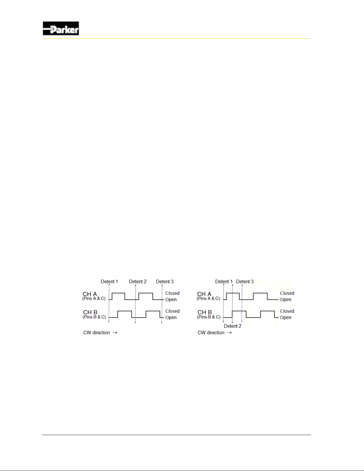
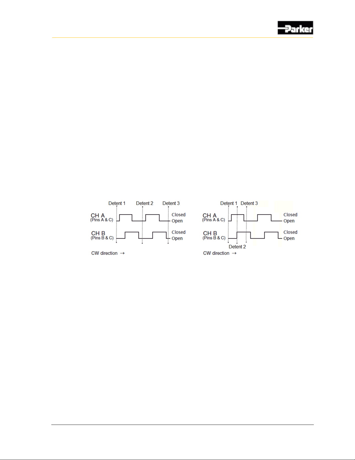
The frequency inputs are provided for the uses of a rotary encoder as an input
device. The encoder states must change 4 times, or once per detent in the shaft
rotation to be recognized by the PHD50, see chart below for the required
waveform.
X2 encoder waveform X4 encoder waveform
Both frequency inputs can also be configured as digital inputs.
Page 23
15
Inputs
3.3. PHD70 inputs
The PHD70 does not support analog inputs.
The PHD70 has up to 8 digital inputs:
▪ GPIO1 through GPIO8
Digital inputs are typically used to read electrical signals from switches.
The PHD70 has 2 frequency inputs:
▪ GPIO9 through GPIO10
The frequency inputs are provided for the uses of a rotary encoder as an input
device. The encoder states must change 4 times per detent in the shaft rotation to
be recognized by the PHD70, see chart below for the required waveform.
X2 encoder waveform X4 encoder waveform
All digital and frequency inputs can also be configured as digital inputs with
wake-up functionality.
Additionally, all inputs can be configured as low power outputs. See section 3.4
for more information.
The different configurations are done in software.
Page 24

16 PHD
Inputs
3.3.1. PHD28/PHD50 analog input capabilities
The PHD28 and PHD50 have analog inputs. These inputs are also configurable as
digital inputs.
Analog inputs are useful for reading potentiometers and Hall Effect signals.
The following table provides specifications for the analog inputs:
Analog Input Specifications
Item
Min
Nom
Max
Unit
Input voltage range
0 5
V
Input pin capacitance
10
µF
Pull-down resistance
26.2
k
Response to step change
50
ms
Over-voltage
36
V
Resolution - 10 bit
5
mV
Offset error
11
mV
Accuracy
3
%
3.3.1.1. Analog input connections
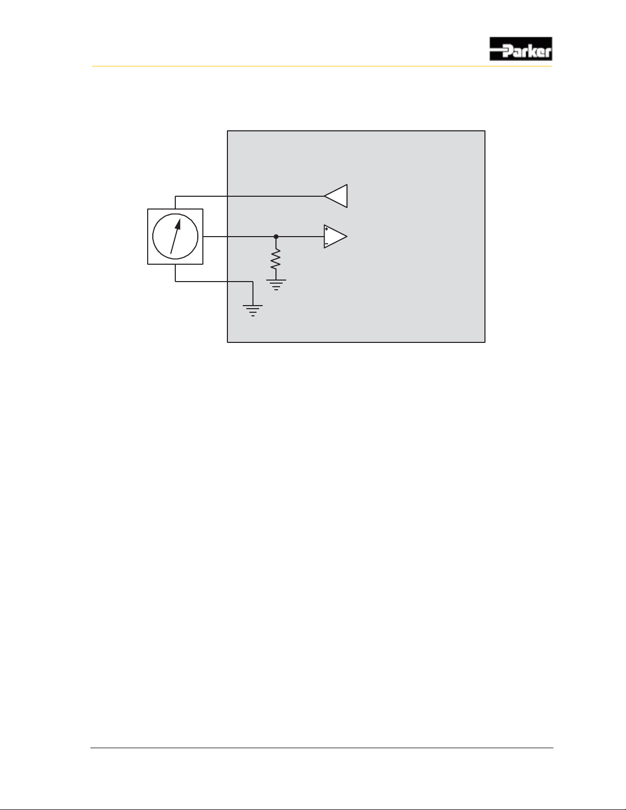
Analog inputs are susceptible to system noise, which can affect the accuracy of
the signal. Signal accuracy can also be affected by ground level shift, which can
cause inputs to activate when they shouldn't.
System noise
To prevent noise pickup on the sensors,
▪ Use the shortest possible wires when connecting analog inputs to sensors.
Page 25
17
Inputs
The following shows how to connect an analog input to reduce system noise:
Internal to product
+5 Vdc Sensor Supply
Sensor Ground
Sensor
Analog Input
Figure 6: Analog input system noise reduction
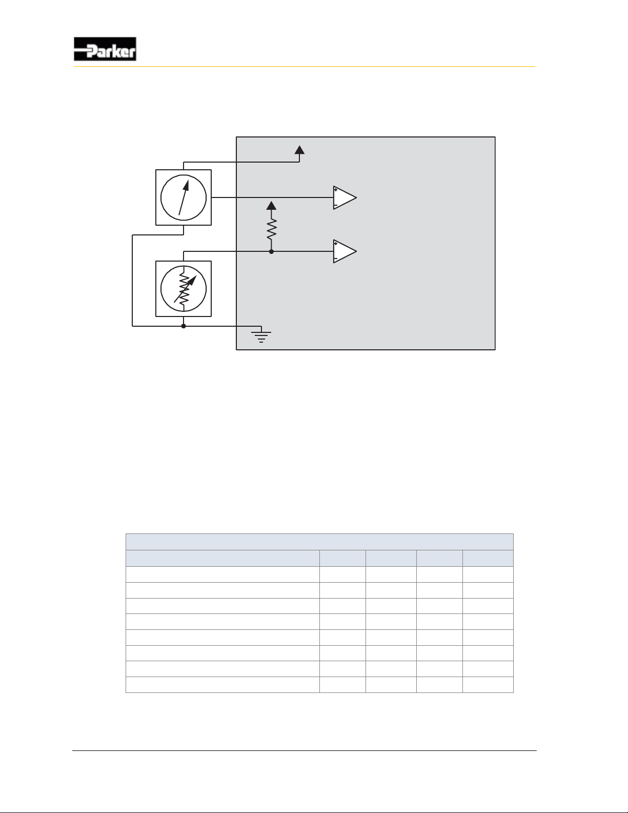
Ground level shift
To reduce ground level shift:
1. Dedicate one of the <Number GND> system ground inputs (GND) to sensors
that have dedicated ground wires, and connect all sensor grounds to this
system ground input.
2. Splice the other system ground inputs together in the vehicle harness (close to
the connector) to provide a better ground for the noisier low-side outputs and
digital circuits.
3. Position the sensor’s ground connection near the system ground connections
to ensure that the signal remains within the digital activation range of the
input.
Note 1: The system ground inputs are rated for low-current signals, which
ensures the sensor's ground is very close in voltage potential to the system
ground.
Page 26
18 PHD
Inputs
Note 2: Sensors that don’t have a dedicated ground wire are typically
grounded to the vehicle chassis through the sensor’s body.
Internal to product
Sensor Power
Resistive Sensor
Pull-up
Resistor
Active Sensor
Analog Input
Analog Input
Figure 7: Analog input ground shift connection for sensors that have dedicated ground wires
3.3.2. PHD28/PHD50/PHD70 digital input capabilities
All of the PHD family of displays have digital inputs that can be configured as
active high or active low. The digital inputs can also be configured as other types
of inputs.
The number of digital inputs depends on PHD model and configuration using the
software tool.
The following table provides specifications for the PHD's digital inputs:
Digital Input Specifications
Item
MIN
NOM
MAX
UNIT
Input voltage range
0 32
V
Pull-down resistance
26.2
kΩ
Pull-up resistance (to 4.3V min / 5V max)
1.2
kΩ
Negative threshold
1.545
V
Positive threshold
4.008
V
Cutoff frequency (hardware)
1590
Hz
Over-voltage
36
V
Wetting current (through pull-up)
4.3
mA
Page 27
19
Inputs
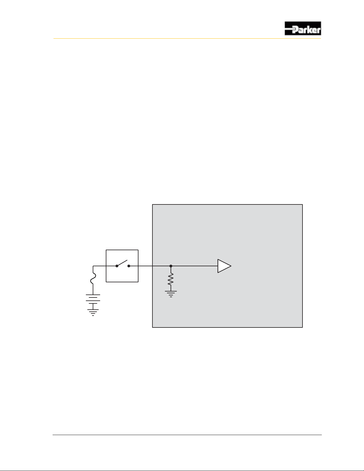
3.3.2.1. Active-High Digital Input Connections
A digital input is typically connected to a switch that is either open or closed.
▪ When an active-high switch is open, the pull-down resistor ensures that no
voltage exists on the input signal, which will be interpreted by the PHD as
inactive.
▪ When the switch is closed, the input is connected to battery voltage, which
will be interpreted by the PHD as active.
For an input that is active-high
▪ It must be connected to battery power so that there is a battery connection
when the state of the input changes.
▪ The power provided to the digital switch connected to the input must be
provided through a fuse in the wire harness.
A typical active-high digital input connection is shown below:
Internal to product
Active High
Digital Input
Battery
Application Switch
Figure 8: Active high digital input
Page 28

20 PHD
Inputs
3.3.3. PHD50/PHD70 frequency input capabilities
The PHD50 and PHD70 have 2 frequency inputs. These inputs are also
configurable as digital inputs. The frequency inputs are ideal for use with halleffect type sensors.
The following table provides specifications for the frequency inputs:
Frequency Input Specifications
Item
MIN
NOM
MAX
UNIT
Input range
0 5 32
V
Negative threshold
1.545
V
Positive threshold
4.008
V
Input capacitance at pin
0.1
µF
Over-voltage
36
V
Frequency accuracy
3
%
Frequency range (see note)
0 1500
Hz
Pull-up resistor to min 4.3V, max 5V
1.2
kΩ
Pull-down resistor
26.2
kΩ
Note: Electrically signals to 0 are possible, but the software will limit the minimum
measurable frequency
3.3.3.1. DC-Coupled Frequency Input Connections
When connecting DC-coupled frequency inputs, be aware of system noise and
ground level shift.
System Noise
DC-coupled frequency inputs are more susceptible to system noise than digital
inputs.
To reduce system noise:
▪ Connect DC-coupled frequency inputs to sensors that produce signals with no
DC offset.
▪ Use the shortest possible wires when connecting DC-coupled frequency inputs
to sensors to prevent noise pickup on the sensors.
Ground Level Shift
Ground level shift affects the accuracy of DC-coupled frequency inputs. Ground
level shift refers to the difference between the system ground input (GND)
voltage, and the sensor ground voltage.
Page 29
21
Inputs
To reduce ground level shift:
▪ If there are more than 1 GND pins in the system, dedicate one of them to
sensors that have ground wires, and connect all sensor grounds to that system
ground pin.
▪ Splice the other system ground inputs together in the vehicle harness (close to
the connector), to provide a better ground for the noisier low-side outputs and
digital circuits.
▪ Ensure the sensor’s ground connection is close to the system ground
connections. This will help ensure the signal remains within the digital
activation range of the input.
Note 1: The PHD system ground inputs are rated for low-current signals,
which ensures the sensor’s ground is very close in voltage potential to the
system ground.
Note 2: Sensors that don’t have a dedicated ground wire are typically
grounded to the vehicle chassis through the sensor’s body.
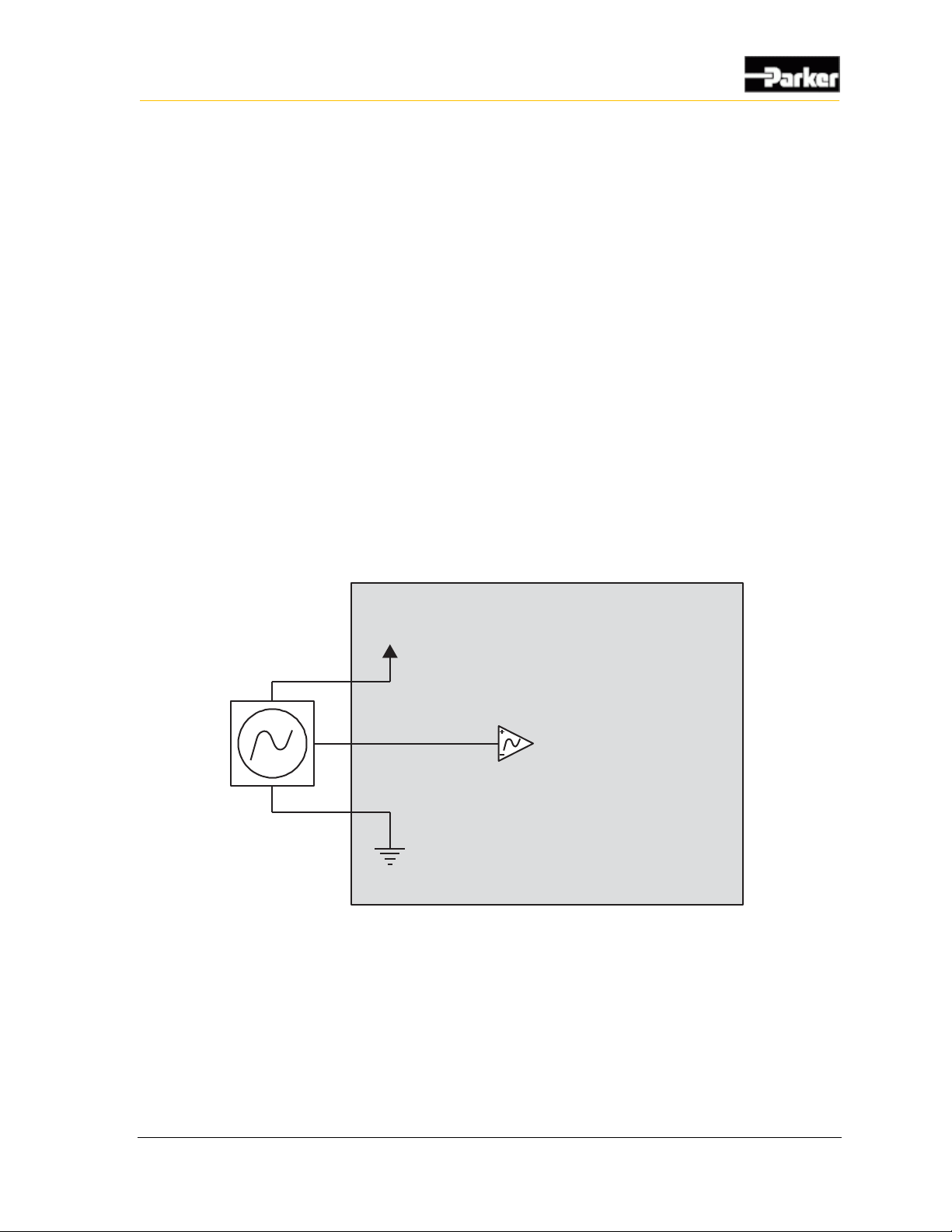
The following shows a typical DC-coupled frequency input connection:
Internal to product
Sensor Voltage
Sensor Ground
Hall Effect Sensor
DC Coupled
Frequency Input
Figure 9: DC-coupled frequency input installation connections
Page 30

22 PHD
Inputs
3.4. Using inputs as low power outputs
Certain input pins, (GPIO1 through GPIO7) of the PHD28 and (GPIO2 through
GPIO6) of the PHD50, may be used as high side, low voltage / low current
outputs. All of the inputs (GPIO1 through GPIO10) of the PHD70 may be used this
way.
A software configurable internal pull-up to 5V provides the drive for this flexible
usage of the pins. These outputs are suitable for driving LEDs and other small
loads.
3.4.1. Low power, high-side output capabilities
The following table provides specifications for the inputs when used as low power
outputs.
Low Power Output Capabilities
Item
Min
Nom
Max
Unit
Operational voltage range
9 32
V
Output resistance w.r.t. GND (output off)
26.2
k
Output voltage
4.3 5.0
V
Output current
358
mA
Leakage current (output off)
1
µA
Output pin capacitance
10
nF
3.4.1.1. Low power, high-side output connections
You must be aware of the following when connecting the low power, high-side
outputs:
▪ the outputs are connected to the internal +5 Vdc supply through a pull-up
resistor. Each output is de-rated to 4.3 V. Maximum load on each output is
358 mA.
▪ the outputs can provide power to LED or other small loads in a vehicle.
When connecting the low power, high-side outputs, ensure you follow these best
practices:
▪ the outputs should not be connected to loads that will draw currents greater
than the maximum current.
▪ The grounds for the loads should be connected physically close to the PHD
power grounds.
Page 31
23
Inputs
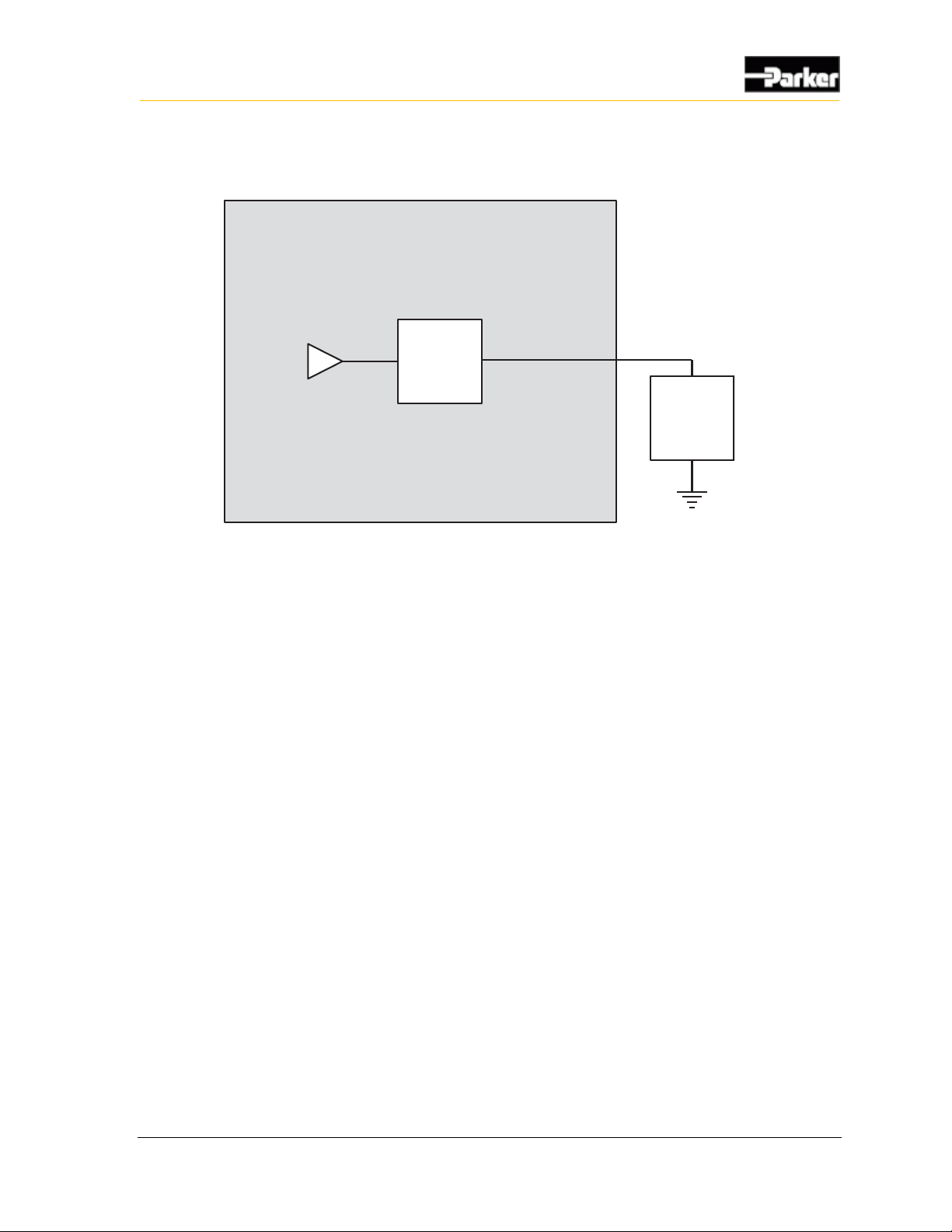
The following shows a typical high-side output connection:
Internal to product
High-Side
Output
Application
Load
Figure 10: High-side output installation connections
Page 32

24 PHD
Outputs
There are 2 types of outputs on the PHD family of displays.
▪ Low-side outputs
▪ Sensor supply outputs
4.1. PHD28/PHD50/PHD70 Low-side outputs
The PHD family has two low-side outputs, with the following pin assignments:
▪ OUTPUT1 through OUTPUT2
4.1.1. Low-side output capabilities
The characteristics of the PHD low-side outputs are shown in the following
tables.
The outputs have analog feedback for error detection.
4. Outputs
Page 33
25
Outputs
Low-Side Output Parameters
Parameter
Min
Nom
Max
Unit
Output current
500
mA
On resistance
550
m
Max. voltage applied to pin
36
V
Current limit in short-to-ground
condition
1.0
1.5
1.9
A
Max PWM Frequency
2000
Hz
Pull-down resistance (PHD28/50)
402.4
k
Pull-down resistance (PHD70)
436.5
k
Feedback gain (V
micro/Vpin
) (see note)
3/33
V/V
Feedback max readable voltage
33
V
Feedback cut-off (3dB) frequency
32
Hz
Note: V
micro
is the voltage at the micro A/D pin, and V
pin
is at the external connector pin. The
tolerance of the V
pin
measurement using nominal gain is ±0.5 V.
Low-Side Output Error Detection
Driver State
Output Condition
Feedback voltage
Error Detected?
Off
Open
0 V
No
Off
Short-to-battery
Vsw/11
Yes
Off
Short-to-ground
0 V
No
On
Open
0 V
No
On
Short
>Vsw/11 (see note)
Yes
Note: An over-temperature fault results in driver output cycling.
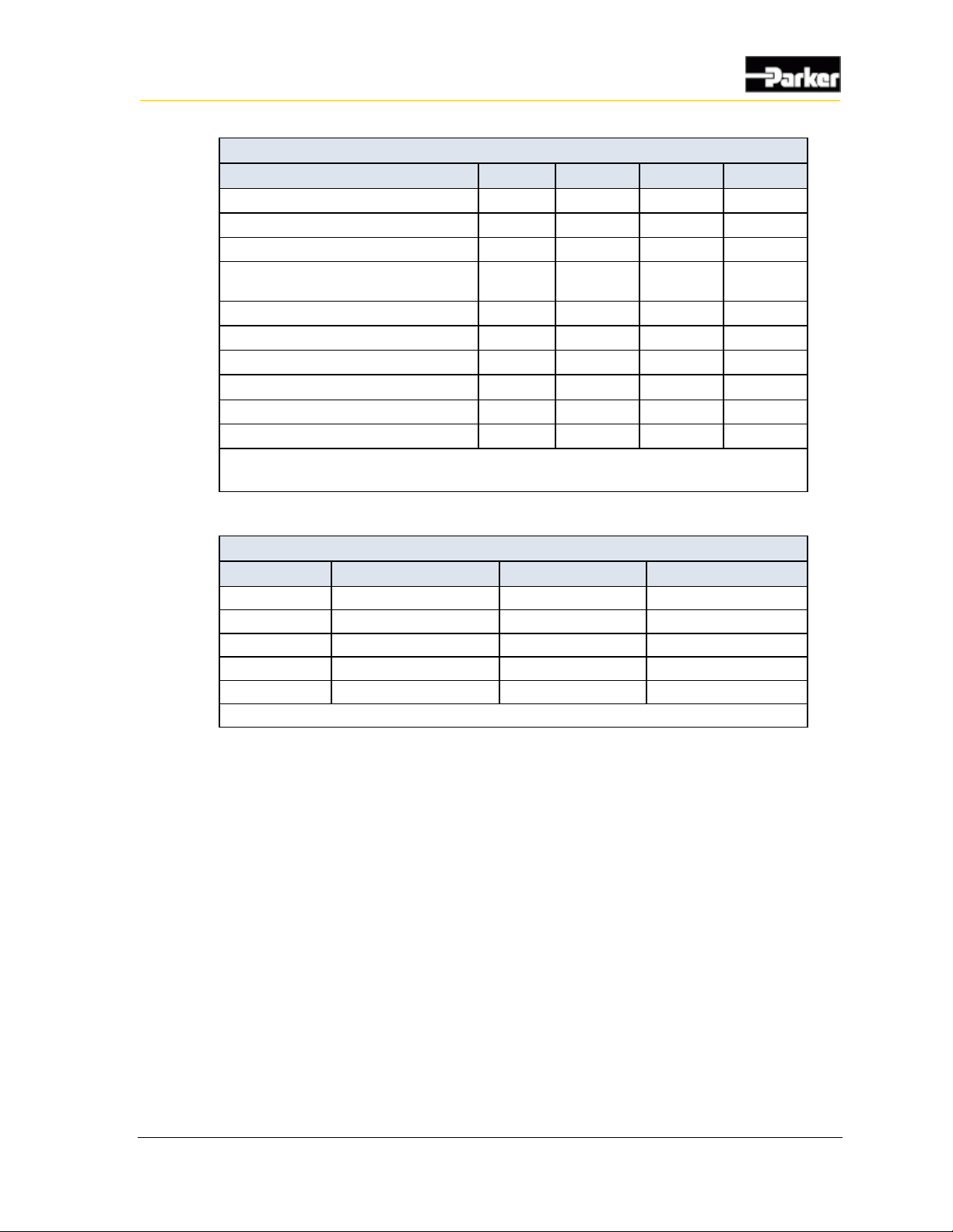
4.1.1.1. Low-side output connections
When connecting low-side outputs, note that
▪ low-side outputs are connected to a common internal ground point that is
connected to the battery ground (GND).
▪ low-side outputs provide switched ground to any load type in a vehicle.
▪ low-side outputs can sink up to 0.5 A.
When connecting a load to a low-side output, ensure that the load will not drive
currents greater than the maximum specified peak current or the maximum
specified continuous current.
Page 34
26 PHD
Outputs
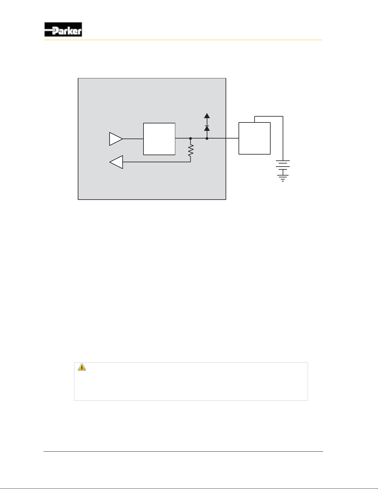
The following shows a typical low-side output connection:
Internal to product
Low-Side
Output
Application
Load
Battery
Figure 11: Low-side outputs with current sense installation connections
4.2. Sensor and regulated supply outputs
The PHD has 2 types of sensor supply pins, labeled USB_VBUS, P5V0 and P12V0
dedicated to providing power to external sensors and devices.
▪ 5V USB or sensor supply
▪ 12V regulated supply
The PHD28 has 1 of each type of supply:
▪ USB_VBUS / P5V0 is a 5V supply
▪ P12V0 is a 12V regulated supply
The PHD50 and PHD70 have 2 x 5V and 1 x 12V supplies:
▪ USB_VBUS and P5V0 are 5V supplies
▪ P12V0 are 2 pins assigned to the 12V regulated supply
Warning! Do not drive more than 500 mA of current through the
combined pins. Doing so will cause the pins to protect themselves by
dropping the voltage, which will result in a lack of power to the sensors
and other devices, causing unknown vehicle responses.
Page 35
27
Outputs
4.2.1. Sensor and regulated supply capabilities
USB_VBUS and P5V0 are 5 V linear power supplies capable of continuously
providing 500 mA to external sensors and the USB port.
5 V Sensor/USB Supply Output Parameters
Parameter
Min
Nom
Max
Unit
Output voltage
4.5
5.0
5.5
V
Current limit
500
mA
P12V0 are 2 pins assigned to the 12 V linear power supply capable of
continuously providing 500 mA to external devices.
12 V Regulated Supply Output Parameters
Parameter
Min
Nom
Max
Unit
Output voltage (see note)
10.8
12.0
13.2
V
Current limit (total of both pins)
500
mA
Note: the 12 V sensor supply is offset 1.3 V from VBATT. In low voltage conditions the
voltage drop can result in the sensor supply going below minimum range.
Page 36
28 PHD
Power
The PHD family is powered by a direct battery connection. The display is turned
on by applying power to one of the wake-up inputs or a CAN message, depending
on configuration in software. The direct battery input is protected against vehicle
transients such as load dump and inductive load switching, etc. It is also protected
against reverse battery voltage of -33 V through the use of a high-current path that
will cause an external fuse to blow.
The PHD operates in a 12 V or 24 V system and can operate from 9 V up to 32 V
with over-voltage protection at 33 V.
Direct Battery Input (+VBATT)
Parameter
Min
Nom
Max
Units
Input voltage for normal operation
9 - 32
V
Minimum cranking voltage (see note 1)
7 -
V
Over-voltage protection
- - 33
V
Reverse battery protection (see note 2)
- - -33
V
Maximum continuous current (see note 3)
VBATT=13.8 V
VBATT=27.0 V
0.44
0.22
1.781
0.93
A
A
Sleep mode current draw (12 V)
<10
mA
Rating of External Fuse
- - 3
A
Note 1: The unit will operate below 9 V, down to 7 V, but the LCD back-lighting may be dim.
Note 2: A reverse battery condition causes an external fuse to blow.
Note 3: This is the maximum expected value, not including the additional draw of the outputs, or
the regulated 5VDC and 12VDC supplies.
5. Power
Page 37

29
Communication
The types of communication available to the PHD family are Controller Area
Network (CAN) communication and USB host.
6.1. Controller Area Network
The PHD28 and PHD50 have 1 Controller Area Network (CAN) communication
port available. The PHD70 has 2 CAN communication ports available.
The PHD family hardware provides controller area network (CAN)
communication according to the SAE J1939 specification, making the PHD
compatible with any CAN-based protocol through software.
CAN communication is used to communicate the status of multiple modules that
are connected together in the same network.
6.1.1. CAN capabilities
The CAN communicates information at a selectable rate from 125 kbps to 1000
kbps. Lack of regular CAN communication is an indication that there is either a
problem with a module in the network, or a problem with the CAN bus.
CAN communication provides a feature called Wake on CAN, which is a way to
provide power control to the PHD.
Wake on CAN provides a low-current sleep mode that turns on the PHD when a
CAN message is received by the module.
It is not possible to filter messages that are used to turn on the PHD using Wake
on CAN. For this reason, any message will turn on the PHD. The application
software must be written to determine how the PHD will behave when it is turned
on.
6. Communication
Page 38
30 PHD
Communication
The following table provides specifications for the CAN:
CAN Specifications
Item
MIN
NOM
MAX
UNIT
Baud rate limitations (hardware)
- - 1000
kbps
Baud rate limitations (software)
125 - 1000
kbps
Wake on CAN current draw
- - 500
uA
Termination resistor
120 - -
Ω
6.1.2. PHD CAN installation connections
The CAN connection for the PHD should conform to the J1939 standard. The
J1939 standard is a robust automotive specification that is a good CAN
installation guideline even when the J1939 CAN protocol is not being used.
For a list of J1939 connection considerations, refer to the SAE J1939
specifications available through the Society for Automotive Engineers. SAE
J1939-11 covers the physical aspects of the CAN bus including cable type,
connector type, and cable lengths.
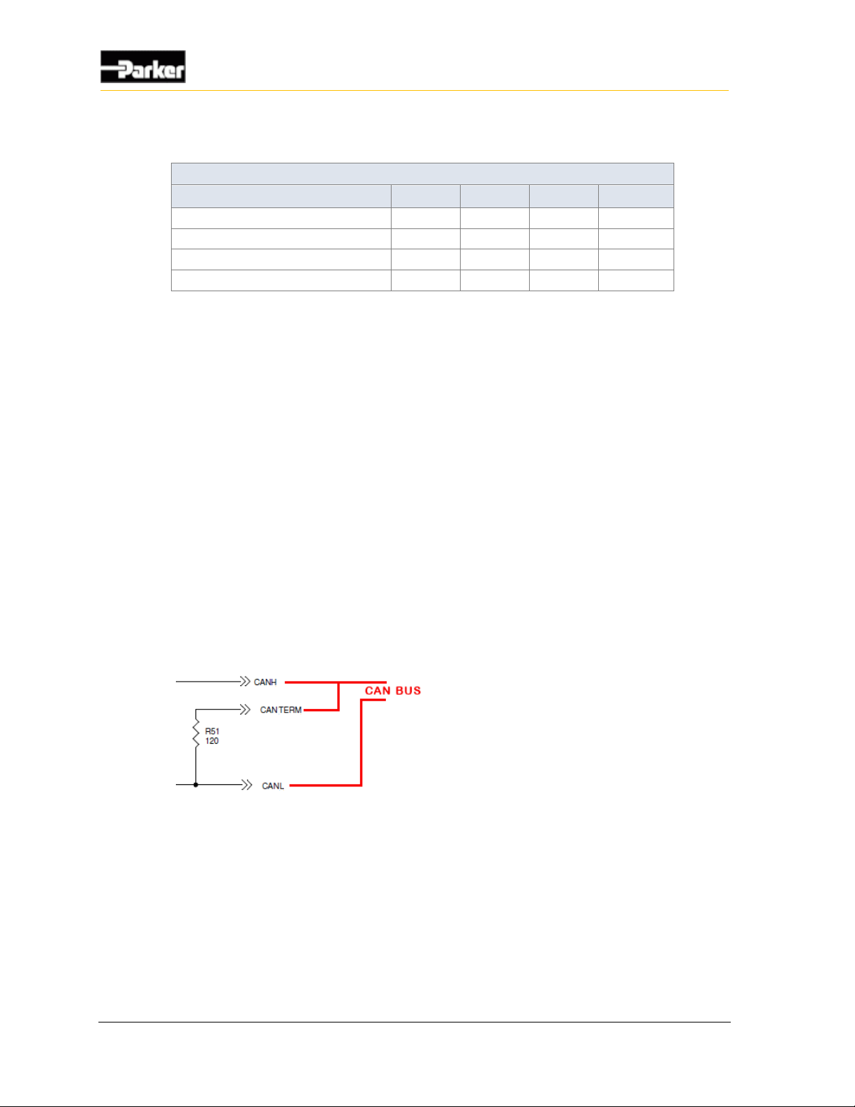
Note: The standard variant of the PHD does not have a CAN termination
resistor, which is based on the assumption that the CAN bus is terminated in
the harness. The PHD displays have a CAN termination pin that allows the
internal termination resistor to be applied. To implement the internal CAN
termination resistor, The CAN_TERM pin should be wired as shown.
Figure 12: PHD CAN_TERM wiring
Page 39

31
Communication
The following lists the elements that are required for a J1939 CAN connection:
▪ CAN Cable: A shielded twisted-pair cable should be used when connecting
multiple modules to the CAN bus. The cable for the J1939 CAN bus has three
wires: CAN High, CAN Low, and CAN Shield (which connect to the
corresponding CAN_HIGH, CAN_LOW, and CAN_SHIELD pins on the
connector). When a module does not have a CAN_SHIELD pin, the CAN
Shield should be connected to an available ground terminal attached to the
negative battery. The CAN cable must have an impedance of 120 Ω.
▪ The CAN cable is very susceptible to system noise; therefore, CAN shield
must be connected as follows:
a. Connect CAN Shield to the point of least electrical noise on the CAN bus.
b. Connect CAN Shield as close to the center of the CAN bus as possible.
c. Use the lowest impedance connection possible.
Note: Ground loops can damage electronic modules. The CAN Shield can
only be grounded to one point on the network. If grounded to multiple points,
a ground loop may occur.
▪ CAN Connectors: Industry-approved CAN connectors are manufactured by
ITT Cannon and Deutsch, and come in either T or Y configurations.
▪ CAN Harness: The CAN harness is the main backbone cable that is used to
connect the CAN network. This cable cannot be longer than 40 meters and
must have a 120 Ω terminating resistor at each end. The 120 Ω terminating
resistors eliminate bus reflections and ensure proper idle-state voltage levels.
▪ CAN Stubs: The CAN stubs cannot be longer than 1 meter, and each stub
should vary in length to eliminate bus reflections and ensure proper idle state
voltage levels.
▪ Max Number of Modules in a System: The CAN bus can handle a maximum
of 30 modules in a system at one time.
Page 40
32 PHD
Communication
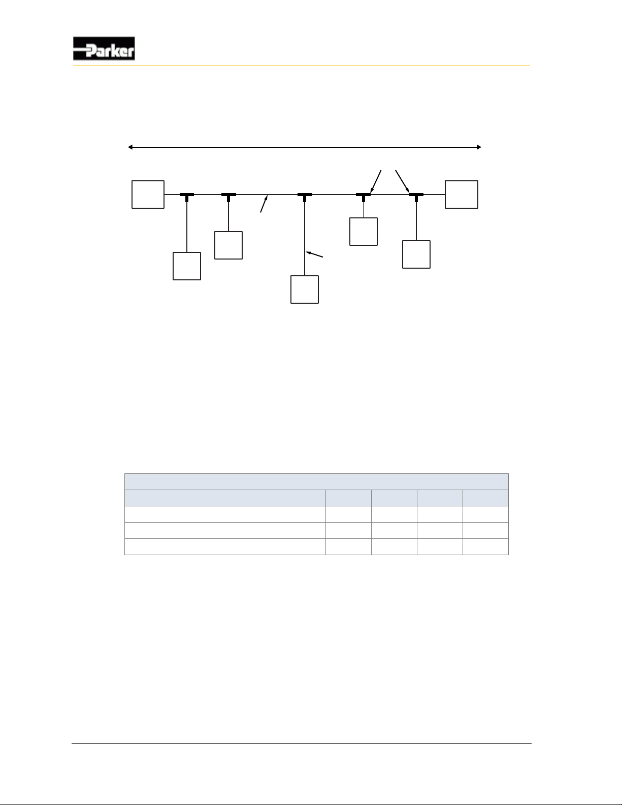
The following shows a typical CAN connection using the SAE J1939 standard:
120 ohm
Terminator
120 ohm
Terminator
Node
Node
Node
Node
Node
T connectors
Variablelength
CAN stub (<1m)
CAN Network Backbone
(less than 40meters long)
Figure 13: J1939 CAN connection
6.2. USB
The PHD family supports one USB port capable of full speed USB 2.0. The USB
port is configured as Host or Device based on settings in software. The USB port
allows you to connect temporarily to the unit for the purpose of retrieving logs,
updating code, or configuring the unit.
The following table provides specifications for the USB port:
USB Device Specifications
Item
Min
Nom
Max
Unit
Communication speed - Full Speed
12
Mbps
Capacitance of I/O to ground
2.5
3.5
pF
Reverse standoff voltage (note 1)
5
V
Note 1: USB connectors are not rated to survive a short to vehicle battery.
To load the application file:
1. Make sure the PHD is powered off and the USB cable is unplugged.
2. Power Up the PHD
3. Connect the USB cable.
4. Send the application file.
5. PHD should reboot in about 20-30 seconds after the file is sent.
Page 41

33
HMI (Human Machine Interface)
The PHD family has an easy to use graphical user interface consisting of a color
LCD and touchscreen with the option of adding a keypad.
7.1. Ambient light sensor
The PHD70 display, if enabled, will automatically adjust the display’s backlight,
based on the amount of ambient light. The ambient light is sensed and measured
via the sensor opening on the glass face. At 1000 lux or greater the backlight is at
full brightness when the auto adjustment is enabled.
7.2. Touchscreen
The display uses a capacitive touchscreen and the host CPU controls the power
and reset with the touchscreen providing an interrupt back to the host. If the
touchscreen interface is required as a wakeup source, then the host must leave
power on the interface and the TP must not be in reset when the host goes to
sleep. There is a series of commands that must be written to the touchscreen
controller to ensure that it’s in its lowest power mode. The interrupt for wakeup
will be driven to the host CPU as well as the power CPU.
7.3. Keypad
The PHD family of displays does not have an internal keypad. The PHD will
support an external keypad (e.g. four button interface, five button interface, 10+
key grid keypad) via the GPIO and any or all of the lines can act as a wakeup
source.
7.4. Buzzer
The PHD units themselves do not house a buzzer. A regulated 12Vdc supply is
provided from the pins of the main connectors and this can be used to power a
buzzer. Note that this interface is limited to 500mA. To drive the other leg of an
7. HMI (Human Machine Interface)
Page 42
34 PHD
HMI (Human Machine Interface)
external buzzer, low-side output 1 or 2 can drive either a steady state low or a
PWM output to drive a buzzer. This low-side output is also capable of sinking
500mA.
7.5. Video
The PHD50 and PHD70 support analog video cameras.
▪ PHD50 has 1 video input
▪ PHD70 has 2 video inputs
The PHD50 supports one D1 resolution PAL/NTSC input.
The PHD70 supports dual D1 resolution PAL/NTSC inputs and can display both
video feeds simultaneously.
7.5.1. Video Input Capabilities
The following table provides specifications for the video inputs:
Video Input Specifications
Item
Min
Nom
Max
Unit
Input voltage range
-5.6 5.6
V
Input resistance
75
Capacitance at pin
65
100
pF
Page 43
35
Serial Ethernet Recovery Flexcan (SERF) Development Board
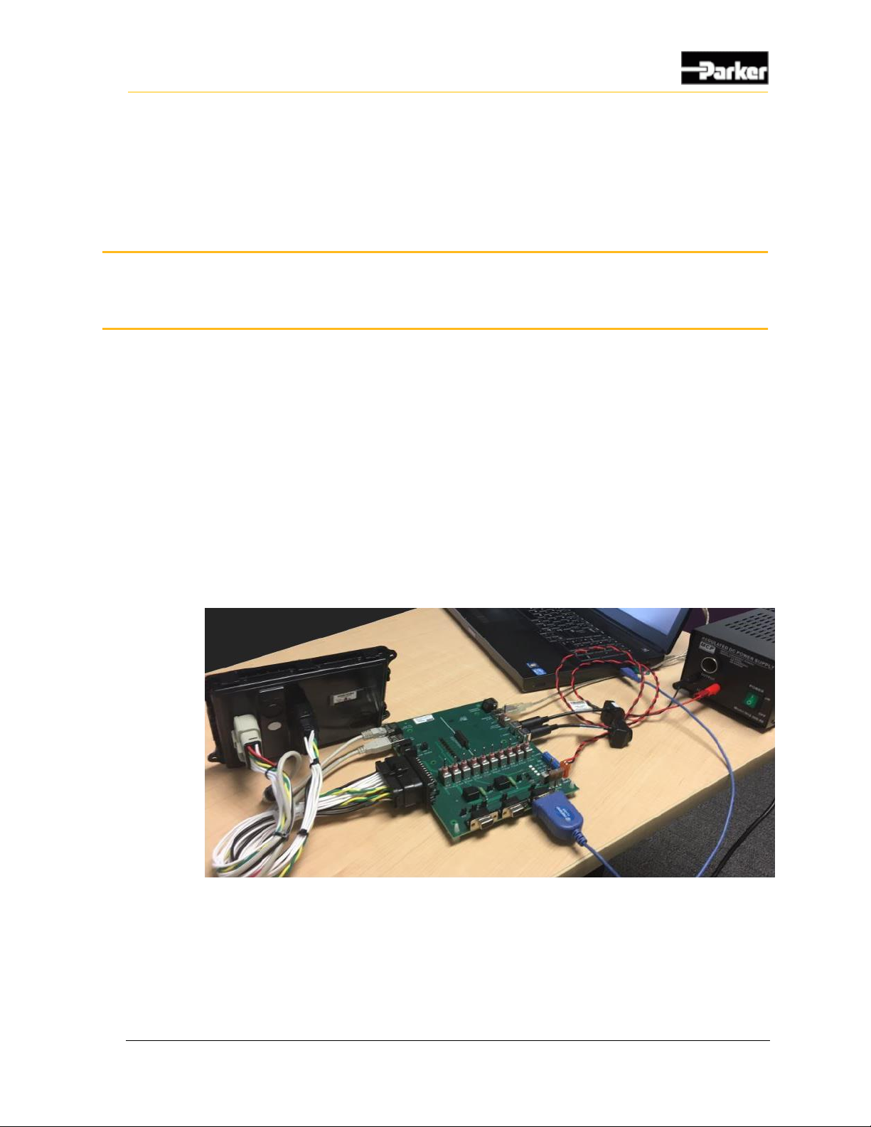
The SERF Development Board for the PHD is intended as a development tool to
simulate inputs and outputs when attached to a PHD display.
8.1. SERF overview
The SERF Development Board allows the GPIO, CAN Bus, video and RS232
inputs and outputs to be easily accessed without having to make a custom wire
harness, or build a special I/O board for each development project. The SERF
Development Board should be used in conjunction with the available Power and
I/O cables for PHD displays. See Catalog HY33-5024-US, PHD Accessories, for
more information.
Figure 14: SERF Development Board connected to PHD
8. Serial Ethernet Recovery Flexcan (SERF)
Development Board
Page 44
36 PHD
Serial Ethernet Recovery Flexcan (SERF) Development Board
8.2. Available Inputs and Outputs
The SERF Development Board offers direct connectivity to the following Inputs
and Outputs for the PHDs.
▪ 5VDC, 12VDC and Ground connections
▪ 12VDC or 24VDC Power Supply
▪ GPIO 1 through 10
▪ RS232 Communication
▪ CAN Bus 1 and 2
▪ CAN Bus 1 and 2 Termination Resistor
▪ Ethernet Communication (Reserved for Future Use)
▪ Audio L and R, Input and Output (Reserved for Future Use)
In addition to the above I/O, the SERF Development Board has pin locations and
power supplies to add on a daughter board for matrix keypad or encoder inputs.
The corresponding I/O is labeled on the SERF Development Board. Note that
“External” indicates the connection from the PHD to an external device such as a
PC, possibly through an adapter cable.
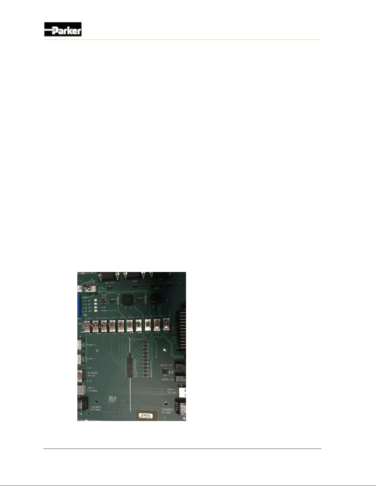
Below is an image of the SERF Development board. All the switches and ports
are labeled. There are several jumpers to enable certain features.
Figure 15: SERF board image showing labels
Page 45
37
Serial Ethernet Recovery Flexcan (SERF) Development Board
8.2.1. Switches and Connectors
The following table describes the corresponding ports and switches associated
with each I/O.
Name
Description
Usage comments
PWR switch
Turns on and off power to the
PHD, 9-32VDC
Power is supplied through JP1 connector. Turns on
Power, but cannot be used as a wake signal.
JP2
connector
Development connector
Connector is reserved for factory use
RS232
connector
Connector for RS232
communication to PC. Note: an
adapter may be required.
Intended for output strings from Lua scripts. For
debugging during development.
CAN 1 and 2
connector
Connector for CAN
Communication to PC. Note: an
adapter may be required.
Intended for tracing CAN messages or inserting CAN
messages to the PHD for development.
GPIO_x
switches
General Purpose I/O inputs.
Used to switch the GPIO to VBATT (high), GND (low) or
floating state during development.
Note: the corresponding jumpers must be positioned as
shown in Jumper section.
JP5
connector
Multi pin connector to the PHD.
Main connector to the PHD connector(s).
Recovery
switch
Connects USB_VBUS for
Recovery, Programming, or
Normal modes.
Switch to V_RCV for recovery mode (>+6Vdc).
Switch to V_USB (+5Vdc) to program PHD28 and
PHD70.
Leave in Neutral to program PHD50 and for normal
operation.
Recovery Switch Operation:
1. With the Power Switch OFF, Place Recovery
Switch in neutral position.
2. Power up the PHD.
3. Place the recovery switch in V_USB position.
4. Send the application file.
5. PHD should reboot in about 20-30 seconds after
the file is sent.
Keep the Recovery Switch in neutral position for normal
boot mode. The V_RCV position is for factory use only.
Video 1 and 2
connectors
Connector for analog cameras.
Used to provide video input from the analog camera to
the PHD.
Audio 1 and 2
connectors
Connector for audio input and
output for the audio.
Not enabled on the Standard products, intended for
future use.
USB external
Connector for USB to PC or
memory stick.
Intended for application downloads from a PC or USB
memory stick in development.
USB to PHD
Connector for USB to the PHD.
Intended for application downloads from a PC or USB
memory stick in development.
Ethernet
external
Connector for Ethernet
connection to PC, gateway or
bridge.
Not enabled on the Standard products, intended for
future use.
Page 46
38 PHD
Serial Ethernet Recovery Flexcan (SERF) Development Board
Name
Description
Usage comments
Ethernet to
PHD
Connector for Ethernet to the
PHD.
Not enabled on the Standard products, intended for
future use.
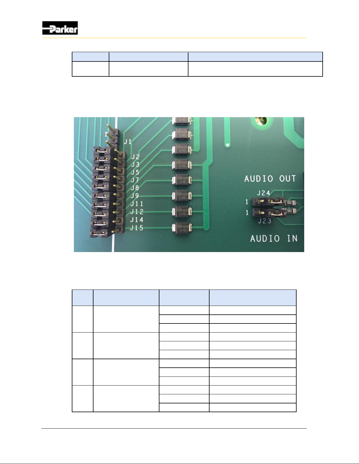
8.2.2. Jumpers
Figure 16: GPIO and audio jumpers
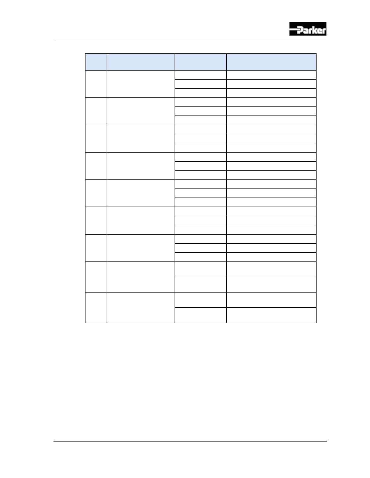
The following table describes the corresponding jumpers associated with each
I/O.
Name
Description
Jumper Position
Pins
Usage Comments
J1
Daughter board power
Removed
Pin 1, 12 Vdc Power
Removed
Pin 2, 5 Vdc Power
Removed
Pin 3, GND
J2
GPIO_10
1 to 2
Enable GPIO switch input.
2 to 3
Intended for factory use.
Removed
Enable daughter board input.
J3
GPIO_9
1 to 2
Enable GPIO switch input.
2 to 3
Intended for factory use.
Removed
Enable daughter board input.
J5
GPIO_8
1 to 2
Enable GPIO switch input.
2 to 3
Intended for factory use.
Removed
Enable daughter board input.
Page 47
39
Serial Ethernet Recovery Flexcan (SERF) Development Board
Name
Description
Jumper Position
Pins
Usage Comments
J7
GPIO_7
1 to 2
Enable GPIO switch input.
2 to 3
Intended for factory use.
Removed
Enable daughter board input.
J8
GPIO_6
1 to 2
Enable GPIO switch input.
2 to 3
Intended for factory use.
Removed
Enable daughter board input.
J9
GPIO_5
1 to 2
Enable GPIO switch input.
2 to 3
Intended for factory use.
Removed
Enable daughter board input.
J11
GPIO_4
1 to 2
Enable GPIO switch input.
2 to 3
Intended for factory use.
Removed
Enable daughter board input.
J12
GPIO_3
1 to 2
Enable GPIO switch input.
2 to 3
Intended for factory use.
Removed
Enable daughter board input.
J14
GPIO_2
1 to 2
Enable GPIO switch input.
2 to 3
Intended for factory use.
Removed
Enable daughter board input.
J15
GPIO_1
1 to 2
Enable GPIO switch input.
2 to 3
Intended for factory use.
Removed
Enable daughter board input.
J23
Audio 1
1 to 2
Not enabled on the Standard
products, intended for future use.
2 to 3
Not enabled on the Standard
products, intended for future use.
J24
Audio 2
1 to 2
Not enabled on the Standard
products, intended for future use.
2 to 3
Not enabled on the Standard
products, intended for future use.
Page 48
40 PHD
Serial Ethernet Recovery Flexcan (SERF) Development Board
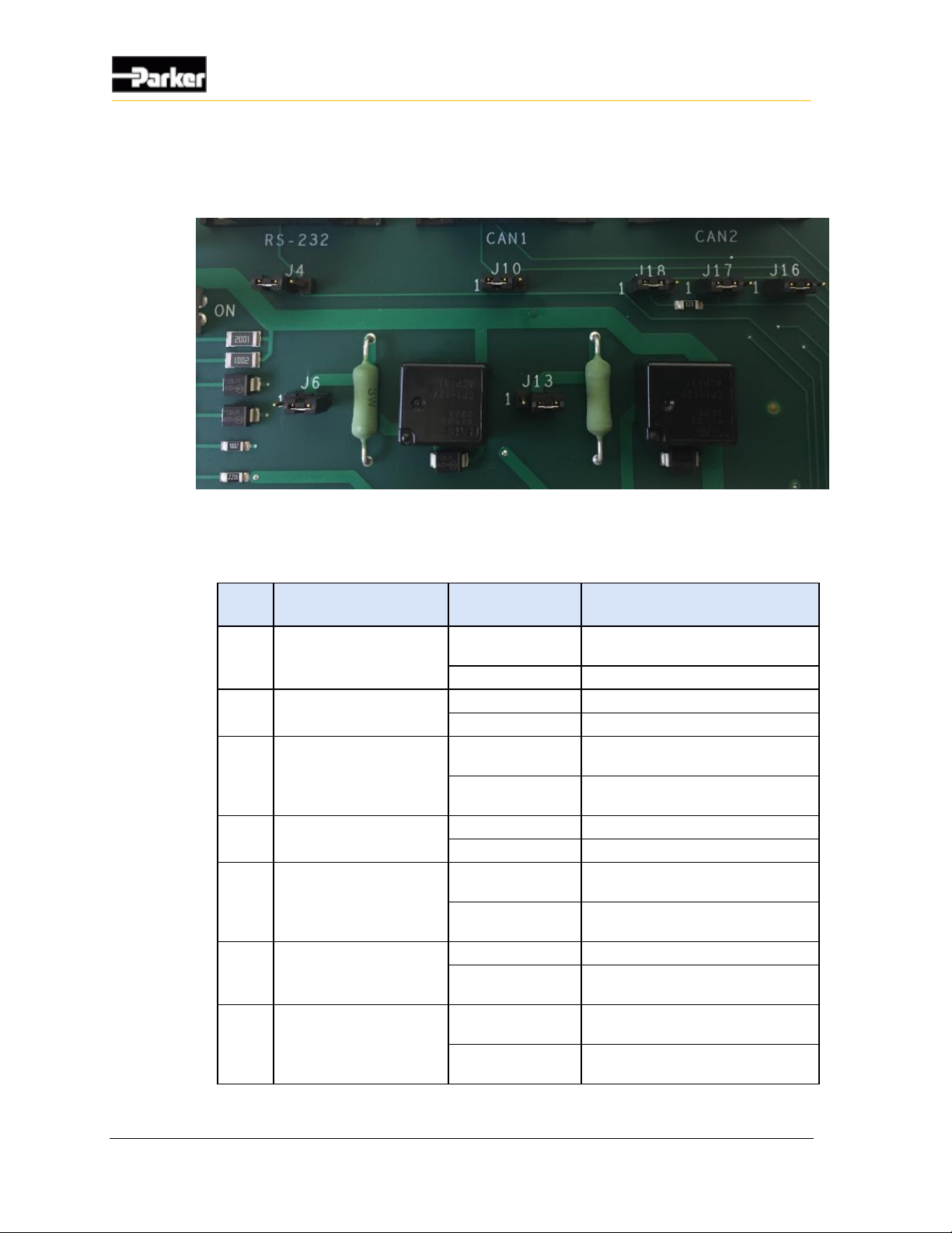
Note: a daughter board with a matrix style keypad or encoder can be connected to
J1 through J12.
Figure 17: Power and communication jumpers
The following table describes the corresponding jumpers associated with power
and communication.
Name
Description
Jumper position
Pins
Usage Comments
J4
RS232
1 to 2
Enable RS232 Input from RS232
Connector.
2 to 3
Intended for factory use.
J6
External power supply
1 to 2
For 12Vdc (nom.) power supply.
2 to 3
For 24Vdc (nom.) power supply.
J10
CAN 1 termination
1 to 2
Disconnect internal termination
resistor to CAN 1.
2 to 3
Connect internal termination resistor
to CAN 1.
J13
External power supply
1 to 2
For 12Vdc (nom.) power supply.
2 to 3
For 24Vdc (nom.) power supply.
J16
CAN 2 high
1 to 2
Connects CAN 1 high to CAN 2
high.
2 to 3
Disconnects CAN 1 high to CAN 2
high.
J17
CAN 2 low
1 to 2
Connects CAN 1 low to CAN 2 low.
2 to 3
Disconnects CAN 1 low to CAN 2
low.
J18 CAN 2 termination
1 to 2
Disconnect external termination
resistor to CAN 2.
2 to 3
Connect internal termination resistor
to CAN 2.
Page 49
41
Serial Ethernet Recovery Flexcan (SERF) Development Board
8.2.3. DB9 Pinout Reference
Both the CAN and RS232 connectors use standard DB9 connectors for ease of
use. Most of the common adapters for either RS232 or CAN that are required to
interface with a PC offer this connection type.
The following table shows the pin outs for each of the DB9 connectors.
CAN
RS232
Pin
Description
Pin
Description
1
No connect
1
No connect
2
CAN L
2
TX (transmit)
3
No connect
3
RX (receive)
4
No connect
4
No connect
5
Shield
5
GND (signal ground)
6
No connect
6
No connect
7
CAN H
7
No connect
8
No connect
8
No connect
9
No Connect
9
No connect
Page 50

42 PHD
Mounting the PHD
To mount the PHD into a vehicle mounting panel,
1. Install the PHD from the front.
2. Ensure that:
the PHD is oriented to the operator's viewing angle
the wire harness connects easily to the connectors and that the bend radius
is adequate
the harness is shielded from harsh impact
3. Secure the PHD using 4 screws or metal spring clips.
4. Install the bezel, typically provided by the customer (Parker does sell a snap-
on cosmetic bezel as an optional accessory).
The PHD may also be mounted from the rear of the panel without a bezel for a
flush appearance using insert studs and nuts.
Refer to the PHD drawing for panel cut-out dimensions:
Drawings and other documents may be found at www.parker.com/ecd or contact
your Parker representative.
9. Mounting the PHD
Page 51
43
Mounting the PHD
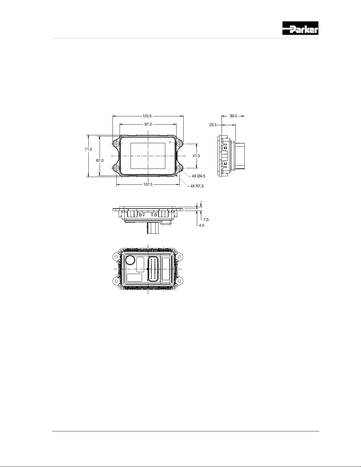
9.1. Dimensions
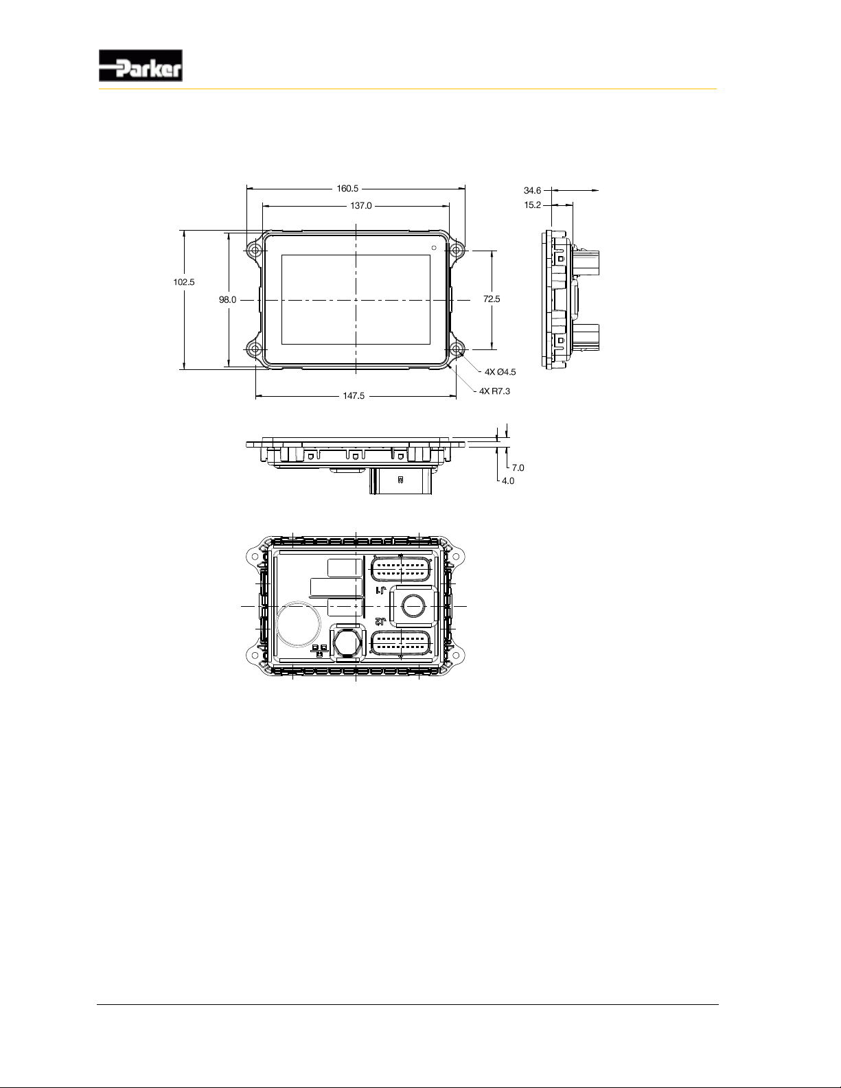
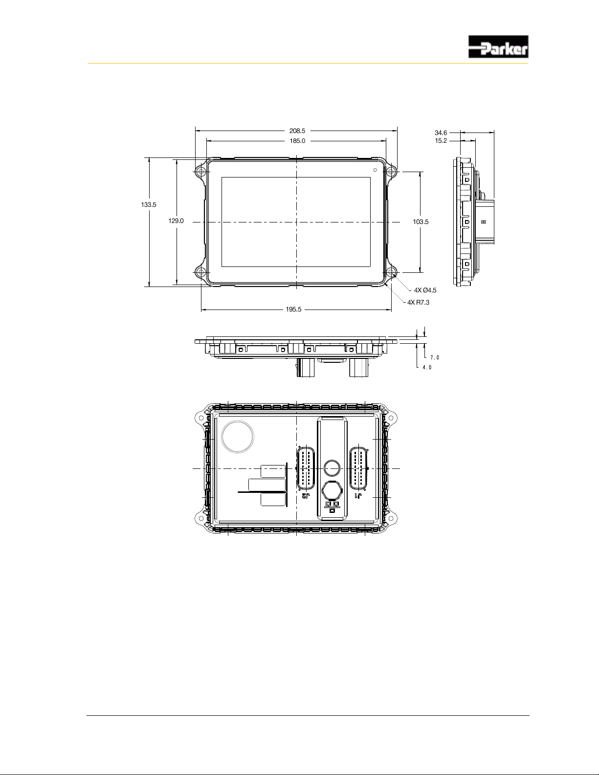
The dimensions for each of the PHD family of displays is provided below.
9.1.1. PHD28
Figure 18: PHD28 dimensions (mm)
Page 52
44 PHD
Mounting the PHD
9.1.2. PHD50
Figure 19: PHD50 dimensions (mm)
Page 53
45
Mounting the PHD
9.1.3. PHD70
Figure 20: PHD70 dimensions (mm)
Page 54

46 PHD
Understanding PHD software
The PHD family of displays is a versatile product suitable for any machine where
a visual HMI for the operator is desired. This manual does not cover how to create
software for the PHD, please refer to the separate PHD SDK software User
Manual.
There are a number of ways to create software for this product.
▪ Configuration of CAN messages and the PHD local I/O is done using Lua
script and a provided SDK.
▪ Creation of display pages and their functionality is performed using Crank
Storyboard software. A Crank licence is required to create display pages.
Contact your Parker Vansco Account Representative for more details about
creating software for the PHD.
10. Understanding PHD software
Page 55

47
Environmental protection
The PHD family is manufactured to meet stringent industry standards. A
summary of tested specifications is listed below. More complete information
(severity/duration) of tests will be included in future editions. Please contact your
Parker Vansco representative for more details.
EMI
▪ J1455 Section 4.13.1, Over voltage
▪ J1455 Section 5.10.3, Reverse polarity
▪ J1455 Section 5.10.4, Short circuit
▪ ISO 7637 Section 5.6.x, EP455 Section 5.11.x, Transients
▪ ISO 14982, EMC emissions
▪ ISO 14982, EMC susceptability
Mechanical environment
▪ BS EN7691 Section 6.6.1, Random vibration
▪ EP455 Section 4.11.3.1, Drop test
ESD
▪ EN61000-4-2, Surface and connectors
Climate environment
▪ IEC 60529 Section 14.2.5, Water (IP65)
▪ IEC 68-2-5, UV exposure
▪ IEC 68-2-2 Section 4, High temperature
▪ IEC 68-2-1 Section 2, Low temperature
▪ EP455 Section 5.1.1, Temperature cycle
▪ J1455 Section 4.1.3.2, Temperature shock
▪ EP455 Section 5.13.2, Humidity soak
11. Environmental protection
Page 56

48 PHD
Environmental protection
▪ EP455 Section 4.3.2, Humidity cycle
Chemical environment
▪ MIL_STD 202G M101E-A, Salt spray
▪ ASAE EP455 Section 5.8.2, Chemical exposure - brush
Page 57

49
A
About the PHD (Parker Hannifin Display) • 1
Active-High Digital Input Connections • 19
Ambient light sensor • 33
Analog input connections • 16
Available Inputs and Outputs • 36
B
Buzzer • 33
C
CAN capabilities • 29
Communication • 29
Connectors • 7
Construction regulations • vii
Controller Area Network • 29
D
DB9 Pinout Reference • 41
DC-Coupled Frequency Input Connections • 20
Diagram conventions • 5
Dimensions • 43
E
Environmental protection • 47
G
General safety regulations • vi
H
HMI (Human Machine Interface) • 33
I
Inputs • 13
J
Jumpers • 38
K
Keypad • 33
L
Low power, high-side output capabilities • 22
Low power, high-side output connections • 22
Low-side output capabilities • 24
Low-side output connections • 25
M
Mounting the PHD • 42
O
Outputs • 24
P
PHD CAN installation connections • 30
PHD28 inputs • 13
PHD28/PHD50 analog input capabilities • 16
PHD28/PHD50/PHD70 digital input capabilities • 18
PHD28/PHD50/PHD70 Low-side outputs • 24
PHD50 inputs • 14
PHD50/PHD70 frequency input capabilities • 20
PHD70 inputs • 15
Pinouts • 8
Power • 28
Publication History • v
S
Safety • vi
Safety during installation • vii
Safety during maintenance and fault diagnosis • viii
Safety during start-up • viii
Safety symbols • vi
Sensor and regulated supply capabilities • 27
Sensor and regulated supply outputs • 26
SERF overview • 35
Serial Ethernet Recovery Flexcan (SERF) Development
Board • 35
Switches and Connectors • 37
T
Touchscreen • 33
U
Understanding PHD software • 46
USB • 32
Using inputs as low power outputs • 22
V
Video • 34
Video Input Capabilities • 34
W
Welding after installation • vii
12. Index
Page 58

Parker Hannifin Display
PHD User Guide
MSG33-5021-IB/US
 Loading...