

Page 1

Reference Manual
Parallella-1.x
REV 14.09.09 1
Page 2

Revision History
Version Comments
0.13.2.13 Initial release
1.13.6.24 Updated PEC_POWER Pin outs
Part Numbers Added + Document Links
Changed flash to 128Mb
Replaced 5V DC/USB power mux with pin header
Changed power sub-system
Epiphany now uses 1.8V IO voltage
Added UART 2-pin header
Changed license to creative common
1.13.7.27 Added UART interface back to PEC_POWER
Added test points for SYS_5V and 1P0V
Added 2-pin header for 5V mounting hole
14.04.15 Removed second USB port “PC connection” as supported feature
No longer supporting the USB-OTG (only host mode)
14.09.09 Removed reference to reset button
nd
Remove reference to 2
USB port
Added numerous tables, design details
REV 14.09.09 2
Page 3

Related Documents
Epiphany Architecture Reference Manual:
http://www.adapteva.com/docs/epiphany_arch_ref.pdf
Epiphany SDK Reference Manual:
http://www.adapteva.com/docs/epiphany_sdk_ref.pdf
Epiphany-III Datasheet:
http://www.adapteva.com/docs/e16g301_datasheet.pdf
Epiphany-IV Datasheet:
http://www.adapteva.com/docs/e64g401_datasheet.pdf
Software Repositories:
Parallella Hardware and Software Repository
https://github.com/parallella
Epiphany SDK Software Repository
https://github.com/adapteva
SD Card Images:
ftp://ftp.parallella.org
REV 14.09.09 3
Page 4

Contents
Table of Contents
1 Overview ..................................................................................................................................... 9
Table 1: Parallella Feature Summary ............................................................................................................ 9
Figure 1: The Parallella Board (top view) .................................................................................................... 10
Figure 2: The Parallella Board (bottom view) ............................................................................................. 10
Figure 3: Zynq Connectivity Diagram .......................................................................................................... 11
Figure 4: Parallella High Level Architecture ................................................................................................ 12
2 Quick Start Guide ...................................................................................................................... 13
Step1: Ensure that you have the required accessories ......................................................................... 13
Step 2: Create a bootable micro-SD card .............................................................................................. 13
Step 3: Familiarize yourself with known issues .................................................................................... 13
Step 4. Connect peripherals, fit the heat-sink and apply power .......................................................... 14
Step 5: Build and run a program ............................................................................................................ 14
3 Feature Descriptions ................................................................................................................. 15
3.1 Introduction ................................................................................................................................ 15
3.2 CPU .............................................................................................................................................. 15
3.3 Epiphany Coprocessor................................................................................................................. 17
3.4 SDRAM ........................................................................................................................................ 17
3.5 Flash ............................................................................................................................................ 17
3.6 Gigabit Ethernet .......................................................................................................................... 18
3.7 USB 2.0 Host Port ........................................................................................................................ 18
3.8 Micro SD ...................................................................................................................................... 18
3.9 HDMI Port ................................................................................................................................... 18
3.10 LED Indicators ............................................................................................................................. 18
3.11 Serial Port .................................................................................................................................... 18
3.12 I2C ............................................................................................................................................... 18
3.13 Audio ........................................................................................................................................... 18
3.14 Analog Input ................................................................................................................................ 18
REV 14.09.09 4
Page 5

3.15 JTAG Debugging .......................................................................................................................... 18
3.16 Powering the board .................................................................................................................... 18
3.17 Parallella On-Board Power Management ................................................................................... 19
3.18 Parallella Supply Outputs ............................................................................................................ 20
3.19 Parallella Expansion Connectors ................................................................................................. 20
3.20 Mounting Holes ........................................................................................................................... 22
4 Parallella System Architecture .................................................................................................. 23
4.1 Zynq Memory Map...................................................................................................................... 23
4.2 Epiphany Memory Map .............................................................................................................. 24
4.3 Epiphany Specific FPGA Resources ............................................................................................. 25
5 Board Configuration ................................................................................................................. 27
5.1 FPGA Pin Assignment .................................................................................................................. 27
6 Booting the Parallella ................................................................................................................ 32
7 Parallella Expansion Connector Details .................................................................................... 33
7.1 PEC_POWER ................................................................................................................................ 33
7.2 PEC_FPGA .................................................................................................................................... 36
7.3 PEC_NORTH/PEC_SOUTH ........................................................................................................... 38
8 Electrical and Performance Specifications ............................................................................... 43
8.1 Dimensions and Weight .............................................................................................................. 43
8.2 Power Consumption ................................................................................................................... 43
8.3 Performance Metrics .................................................................................................................. 43
8.4 IC Metrics Summary .................................................................................................................... 44
9 About the Parallella Board ........................................................................................................ 45
9.1 Design Information ..................................................................................................................... 45
9.2 Build Options ............................................................................................................................... 45
9.3 Contributors ................................................................................................................................ 46
9.4 Attributions ................................................................................................................................. 47
9.5 Licensing ...................................................................................................................................... 47
9.6 Disclaimers .................................................................................................................................. 48
9.7 Warranty ..................................................................................................................................... 50
REV 14.09.09 5
Page 6

REV 14.09.09 6
Page 7

List of Figures
Figure 1: The Parallella Board (top view) .................................................................................................... 10
Figure 2: The Parallella Board (bottom view) ............................................................................................. 10
Figure 3: Zynq Connectivity Diagram .......................................................................................................... 11
Figure 4: Parallella High Level Architecture ................................................................................................ 12
Figure 5: Power Management .................................................................................................................... 19
Figure 6: PEC Placement Diagram ............................................................................................................... 21
Figure 7: Parallella Expansion Connectors (PEC) ........................................................................................ 21
Figure 8: Daughter Card Configurations ..................................................................................................... 22
Figure 9: Zynq Memory Map....................................................................................................................... 23
Figure 10: Epiphany Memory Map ............................................................................................................. 24
List of Table
Table 1: Parallella Feature Summary ............................................................................................................ 9
Table 2: Parallella IC summary .................................................................................................................... 15
Table 3: Zynq Feature Summary ................................................................................................................. 16
Table 4: Epiphany System Registers ........................................................................................................... 26
Table 5: Zynq Bank32 Pin Assignments ....................................................................................................... 28
Table 6: Zynq Bank 34 Pin Assignments ...................................................................................................... 30
Table 7: Zynq Bank 13 Pin Assignments ...................................................................................................... 31
Table 8: PEC_POWER Signal Summary ....................................................................................................... 34
Table 9: PEC_POWER Pin Mapping ............................................................................................................. 35
Table 10: PEC_FPGA Signal Summary ......................................................................................................... 36
Table 11: PEC_FPGA Pin Mapping ............................................................................................................... 37
Table 12: PEC_NORTH/SOUTH Signal Summary ......................................................................................... 38
Table 13: PEC_NORTH Pin Mapping for Parallella-16 ................................................................................. 39
Table 14: PEC_NORTH Pin Mapping for Parallella-64 ................................................................................. 40
Table 16: PEC_SOUTH Pin Mapping for Parallella-16 ................................................................................. 41
Table 17: PEC_SOUTH Pin Mapping for Parallella-64 .................................................................................
REV 14.09.09 7
42
Page 8

Table 18: Dimensions and Weight .............................................................................................................. 43
Table 19: Power Consumption .................................................................................................................... 43
Table 20: Paralllella Performance Summary ............................................................................................... 44
Table 21: IC Metrics .................................................................................................................................... 44
REV 14.09.09 8
Page 9
1 Overview
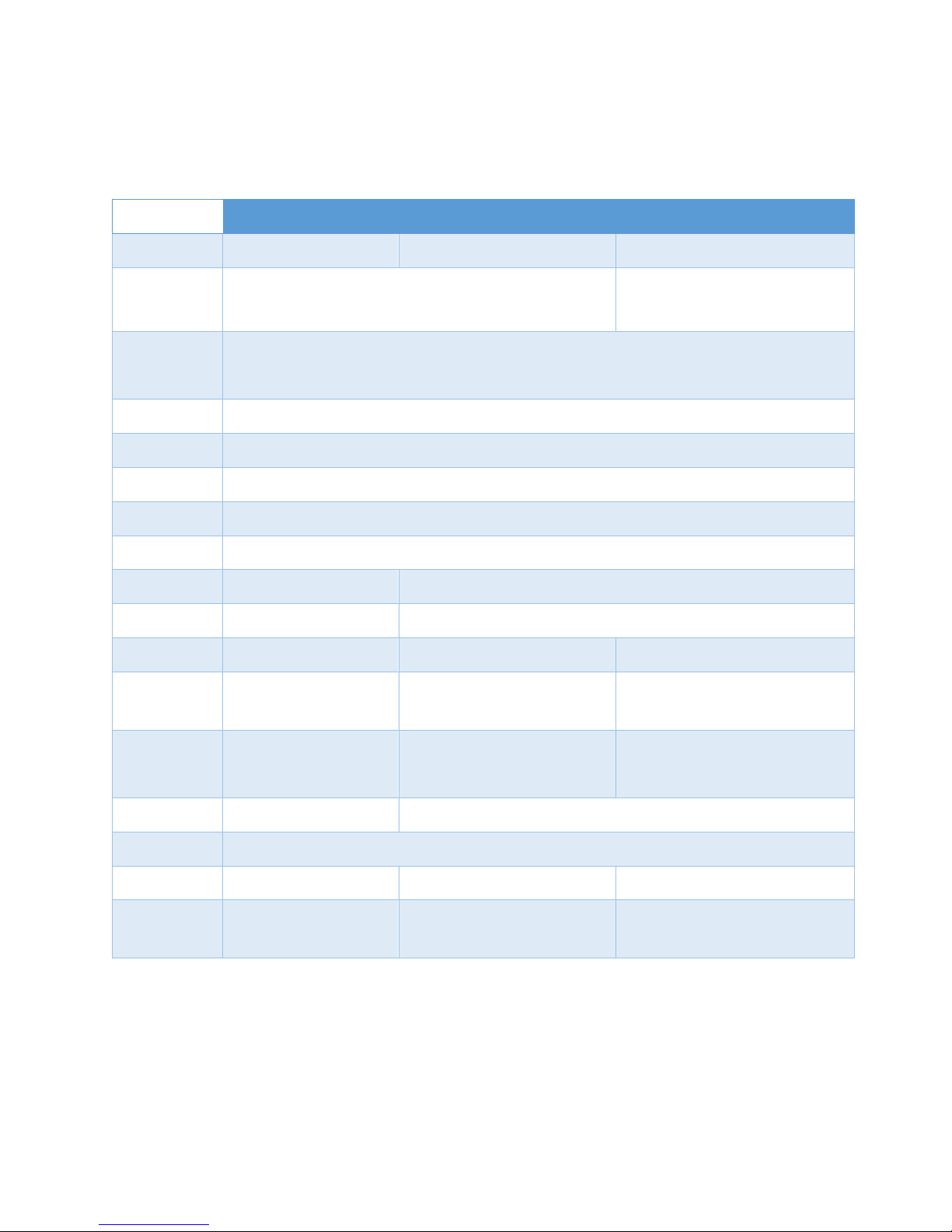
The Parallella board is a high performance computing platform based on a dual-core ARM-A9 Zynq
System-On-Chip and Adapteva’s Epiphany multicore coprocessor. Current commercially available models:
Model
P1600 P1601 P1602
Mnemonic “Microserver” “Desktop” “Embedded”
Host
Processor
Xilinx Zynq Dual-core ARM A9
XC7Z010
Xilinx Zynq Dual-core ARM A9
XC7Z020
Epiphany 16-core CPU
Coprocessor
E16G301
Memory 1 GB DDR3
Ethernet Gigabit Ethernet
Boot Flash 128Mb QSPI Flash
Power 5V DC
Storage Micro-SD
USB No USB 2.0 Host Port
HDMI No Micro HDMI
GPIO Pins 0 24 48
eLink
Connectors
0 2 2
FPGA
Logic
28K Logic Cells
80 DSP Slices
28K Logic Cells
80 DSP Slices
80K Logic Cells
220 DSP slices
Weight 1.3 oz (36 grams) 1.4 oz (38 grams)
Size 3.5″ x 2.1″ x 0.625″ (90mmx55mmx18mm)
SKU P1600-DKxx P1601-DKxx P1602-DKxx
HTS Code
(Schedule B)
8471.41.0150 8471.41.0150 8471.41.0150
Table 1: Parallella Feature Summary
REV 14.09.09 9
Page 10
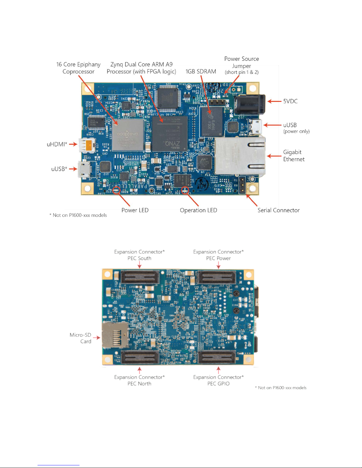
Figure 1: The Parallella Board (top view)
REV 14.09.09 10
Figure 2: The Parallella Board (bottom view)
Page 11
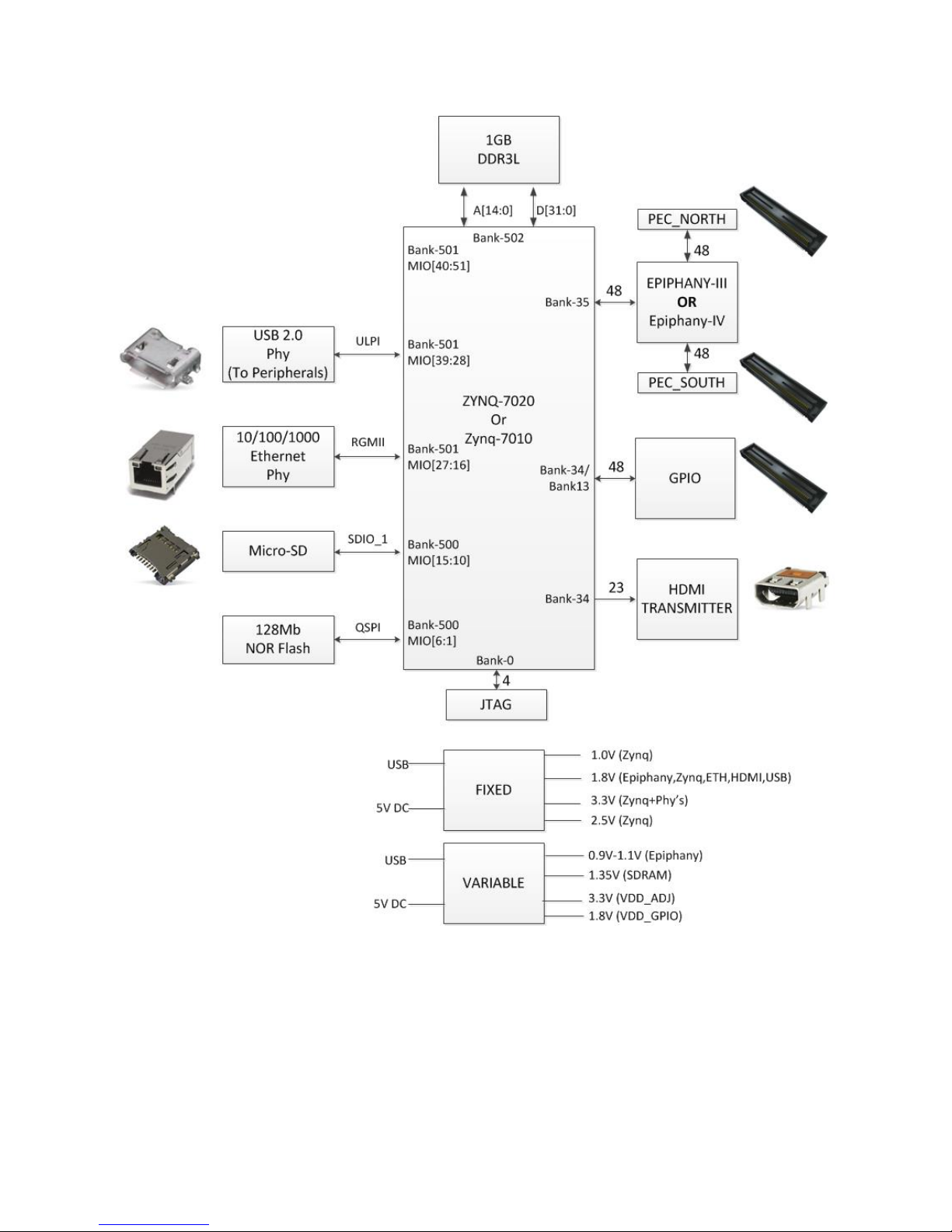
REV 14.09.09 11
Figure 3: Zynq Connectivity Diagram
Page 12

Figure 4: Parallella High Level Architecture
REV 14.09.09 12
Page 13
2 Quick Start Guide
This section is a summary of the quick start guide is found at www.parallella.org/quick-start
Step1: Ensure that you have the required accessories
• A high quality 2000mA rated 5V DC power supply with 5.5mm OD / 2.1mm ID center positive
polarity plug.
• An ethernet cable
• A fan (required for boards sold before July 10th, 2014, recommended for all others)
• A micro HDMI to HDMI cable (not needed for headless option)
• A USB male Micro-B to female Standard-A cable (not needed for headless option)
Step 2: Create a bootable micro-SD card
Burn a fresh Micro-SD card using the latest distribution.
• Instructions for creating an SD card
Note: Burn a fresh SD card even if you were shipped a pre-programmed micro-SD card!
Step 3: Familiarize yourself with known issues
• The board does get hot so you have to take precautions to cool the board properly. Before
letting the board run for hours, you must ensure that the board doesn’t overheat. (preferably by
using the ‘xtemp’ utility
• Boards used without a fan must be placed vertically.
• The Parallella is sensitive to static discharge and must be handled appropriately.
• If you were shipped a board before March 1st, 2014, then you must use a conforming powered
.)
USB hub.
• If you were shipped a board before July 10th, 2014 then you must use a fan with the board. (we
do still recommend a fan for all customers, especially if you are going to push the performance
of the board)
REV 14.09.09 13
Page 14

Step 4. Connect peripherals, fit the heat-sink and apply power
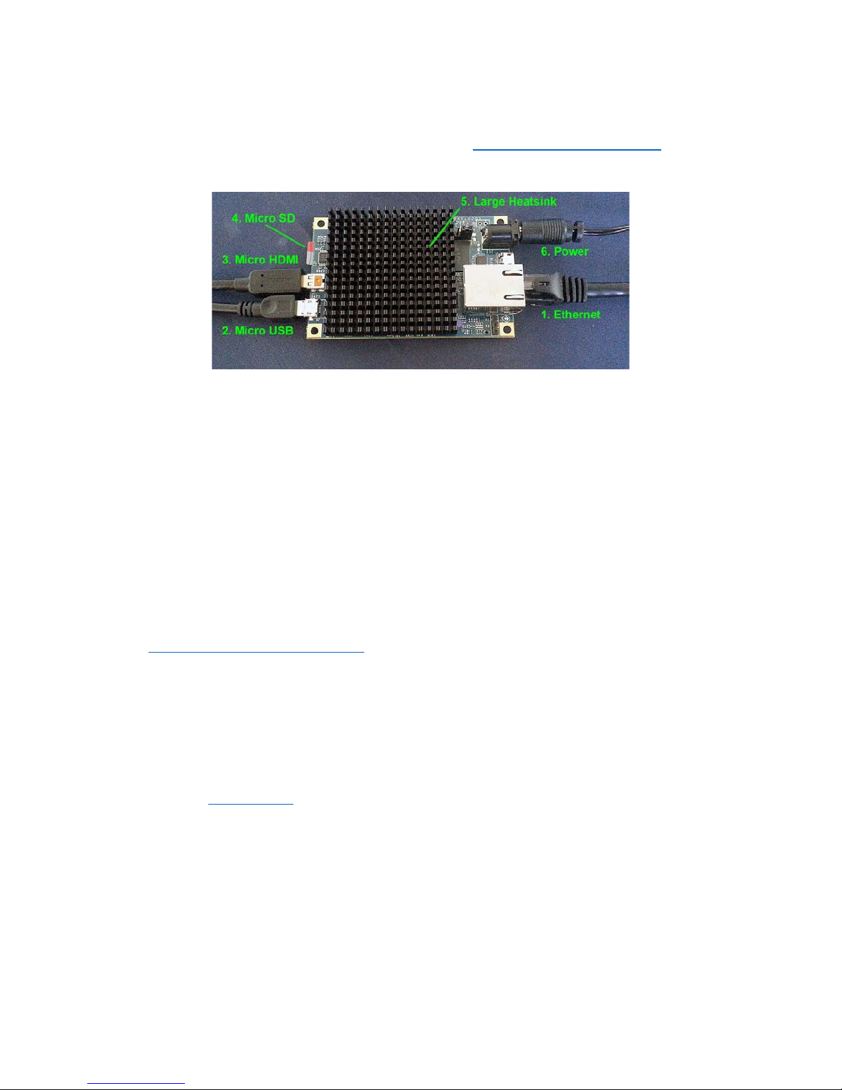
• Connect the cables as indicated by #1-4 in the picture above
• Attach a heatsink to the Zynq device (#5 in right hand picture) OR install the new large heatsink
onto the Parallella board
• Make sure a fan is directed at the board if required. A fan is required when using the small
heatsink (right hand picture above). With the large heatsink (left hand picture above) the board
will function in normal conditions without requiring a fan, depending on your usage. Monitor
the temperature using a utility such as xtemp, and keep the chip temp below 70 degrees Celsius.
• Apply power (#6 in picture)
Step 5: Build and run a program
The system will boot and a login screen will appear.
Login with the username linaro and password linaro.
REV 14.09.09 14
Page 15
3 Feature Descriptions
3.1 Introduction
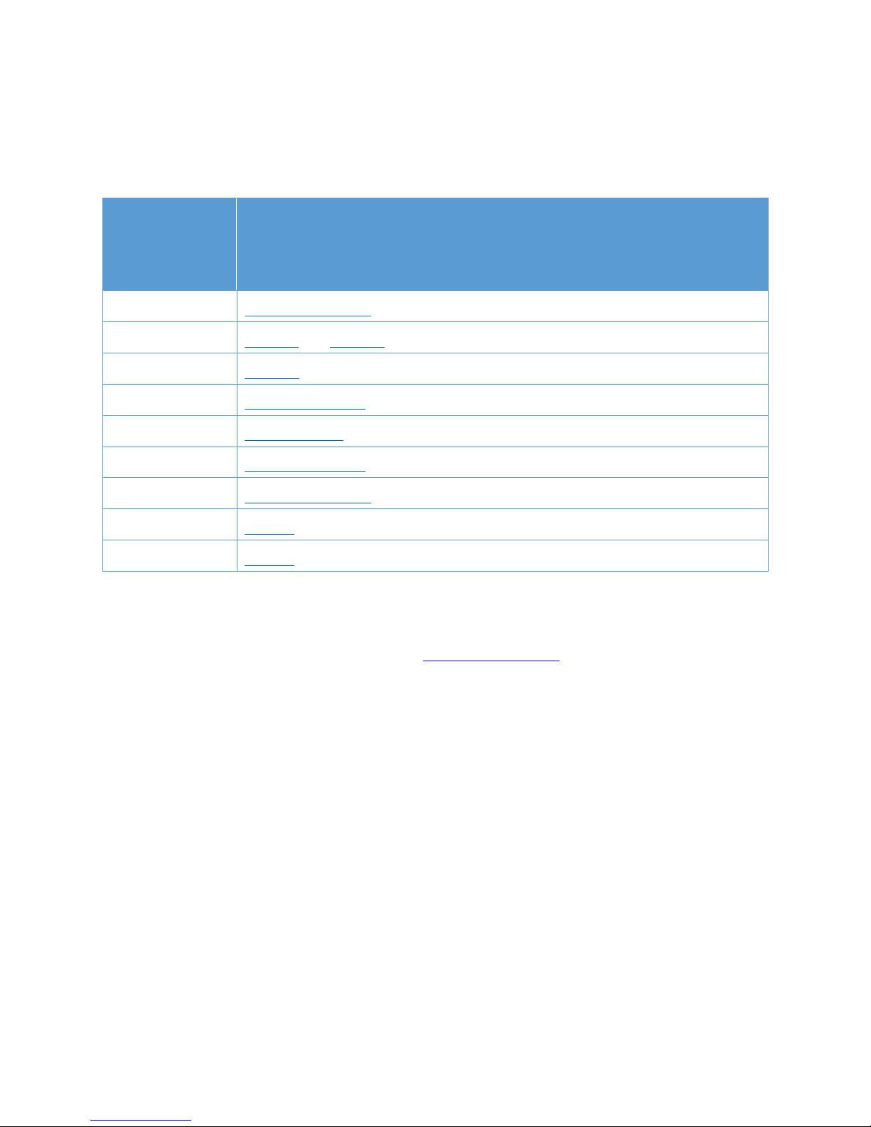
The Parallella-1.x board uses the components listed in the table below.
Device
Part Number (and datasheet link)
CPU Zynq™-7000 AP SoC
Epiphany E16G301 and E64G401
Eth PHY 88E1318
USB PHY
HDMI PHY
SDRAM
Flash
USB3320C-EZK-TR
ADV7513BSWZ
MT41K256M32SLD
N25Q128A13EF840E
PMIC #1 ISL9307
PMIC #2
ISL9305
Table 2: Parallella IC summary
3.2 CPU
The central processor on the Parallella board is the
Zynq™-7000 AP SoC. The Zynq represents a new class
of processor product which combines an industry-standard ARM® dual-core Cortex™-A9 MPCore™
processing system with Xilinx 28nm programmable logic. The Zynq SoC includes the following set of
features:
Dual-core ARM® Cortex™-A9 CPU:
• Coherent multiprocessor support
• ARMv7-A architecture
• 32 KB Level 1 4-way set-associative instruction/data caches (independent for each CPU)
• 512 KB 8-way set-associative Level 2 cache shared between CPUs
• TrustZone® security
• Jazelle® RCT execution Environment Architecture
• NEON™ media-processing engine
• Single and double precision Vector Floating Point Unit (VFPU)
• CoreSight™ and Program Trace Macrocell (PTM)
• Three watchdog timers, one global timer, two triple-timer counters
REV 14.09.09 15
Page 16
I/O Peripherals and Interfaces:
• 10/100/1000 tri-speed Ethernet MAC peripherals GMII, RGMII, and SGMII interfaces
• Two USB 2.0 OTG peripherals
• Two full CAN 2.0B compliant CAN bus interfaces
• Two SD/SDIO 2.0/MMC3.31 compliant controllers
• Two full-duplex SPI ports with three peripheral chip selects
• Two high-speed UARTs (up to 1 Mb/s)
• Two master and slave I2C interfaces
• 8-Channel DMA Controller with scatter/gather capability
• JTAG port for ARM debugging and FPGA programming
• 12 bit ADC input
• On-chip voltage and temperature sensing
Programmable Logic:
• LVCMOS, LVDS, and SSTL signaling with 1.2V to 3.3V IO
• Easily accessible from ARM cores through AXI bus(master or slave)
• Up to 125 programmable IO pins (Z-7020)
• Up to 85K programmable logics cells (Z-7020)
• Up to 560 KB distributed RAM (Z-7020)
• Up to 220 DSP slice and (Z-7020)
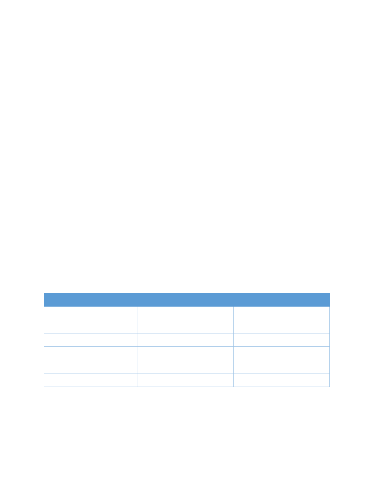
The Parallella board can be built with two different pin compatible Zynq devices: Zynq Z-7010 or the Zynq
Z-7020. The major differences between the Z-7010 and Z-7020 are summarized in Table 4:
Z-7010 Z-7020
Programmable Logic Cells 28K 85K
Look-Up Tables 17,600 53,200
Flip-flops 35,200 106,400
Extensible Block RAM 240KB 560KB
Programmable DSP Slices 80 220
Bank-13 IO Pins No Yes
Table 3: Zynq Feature Summary
REV 14.09.09 16
Page 17

3.3 Epiphany Coprocessor
The Parallella-16 includes the E16G301 device with 16 CPU cores and the Parallella-64 includes the
E64G401 device with 64 CPU cores. Both devices have the following basic features:
Epiphany Core (eCore):
• 32-bit dual-issue superscalar RISC architecture
• Quad-bank 32KB local single cycle access memory
• Floating point instruction set (IEEE754)
• 64-entry register file
• Dual channel DMA engine
• Two 32-bit timers
• Nested interrupt controller
• Memory protection unit
• Debug unit
Network-On-Chip (eMesh):
• Three separate networks:
o rMesh for read transactions
o xMesh for off-chip write transactions
o cMesh for on-chip write transactions
• “API-less” network that processes regular load/store transactions
• All transactions are complete and atomic 104 bit transactions (32 bit address, 64 bit data, and 8
control bits)
• Round robin arbitration at every mesh node
• Mesh network extends off chip enabling glue-less multi-chip design
Chip-To-Chip Links (eLink):
• North, east, west, south links for connecting to other Epiphany chips, FPGAs, or ASICs
• Source synchronous LVDS links with transmit clock aligned in the middle of the data eye
• Dual data rate communication (positive and negative edge transfers)
• Max transfer of 2 bytes transferred in and out simultaneously per link per clock cycle
• Automatic bursting for sequential 64-bit write transactions
3.4 SDRAM
1GB 32-bit wide DDR3L SDRAM
3.5 Flash
128Mb QSPI Flash Memory for boot code
REV 14.09.09 17
Page 18

3.6 Gigabit Ethernet
10/100/1000 Ethernet, RJ45 connector with magnetics.
3.7 USB 2.0 Host Port
Connects to peripheral devices such as mice, keyboard, camera, etc.
3.8 Micro SD
Primary boot source and main Parallella board storage medium.
3.9 HDMI Port
A high quality connection to modern DVI/HDMI monitors and TVs through a micro-HDMI connector.
3.10 LED Indicators
• A green LED controlled by the Zynq GPIO pin.
• A red LED controlled by the Epiphany flag pin
• Two LEDs on the RJ45. The left LED indicates link speed. (amber=1Gb, green=100Mb, off=10Mb).
The right indicates that there is activity on the port.
3.11 Serial Port
A three-pin header for 3.3V UART output from the Zynq.
3.12 I2C
A 5V I2C interface is available through the PEC_POWER connector.
3.13 Audio
Audio is available through the HDMI connector and through the SPDIF pin on the PEC_POWER connector.
3.14 Analog Input
A differential analog input is available on the PEC_POWER connector that is sampled by the Zynq built in
Analog to Digital Converter.
3.15 JTAG Debugging
FPGA programming and debugging of programs running on the Zynq is possible through the JTAG pins on
the PEC_POWER connector.
3.16 Powering the board
The Parallella should be powered through a stable 5V/2A power supply. The following methods are
available for connecting a 5V supply. Current consumption for the Parallella board can be as low as 0.3A
but can reach 1.5A when fully loaded.
REV 14.09.09 18
Page 19
U
29
ISL9307IRTAANFZ-
T
SW1
SW2
VOLDO1
VOLDO2
1P0V
TO: ZYNQ & ETHERNET-PHY
1P8V
3P3V
TO: ZYNQ-BANK500 & SD-CARD & FLASH
2P5V
U
30
ISL9305IRTHWBNLZ-T
TO: ZYNQ-BANK35
ENDCD1
ENDCD2
ENLDO1
ENLDO2
TO: ZYNQ & EPIPHANY-IO &
USB-PHY(S) & HDMI-PHY &
ETHERNET-PHY
PEC_POWER:PIN5
PEC_POWER:PIN6
PEC_POWER:PIN7
PEC_POWER:PIN8
SCL
SDA
FROM ZYNQ PL
FROM ZYNQ PL
SW1
SW2
VOL
DO1
VOL
DO2
VDD_DSP
(1.2V)
1P35V
VDD_GPIO
(2.9V)
VDD_ADJ
(3.3V)
TO: Epiphany Core Supply
TO: Zynq-Bank502 & DRAM
TO: Zynq-Bank34 & Zynq-Bank13
TO: PEC_POWER
Recommended Methods (choose one only):
• J12: 5.5mm OD / 2.1mm ID center positive barrel connector (place jumper on J14 in 1-2 position)
• J7: micro-USB connector (place jumper on J14 in 2-3 position)
Experimental (at your own risk):
• PTH1: Mounting hole. Need to install/solder and short J15
• J13: Pins 1 and 2 of the PEC_POWER connector
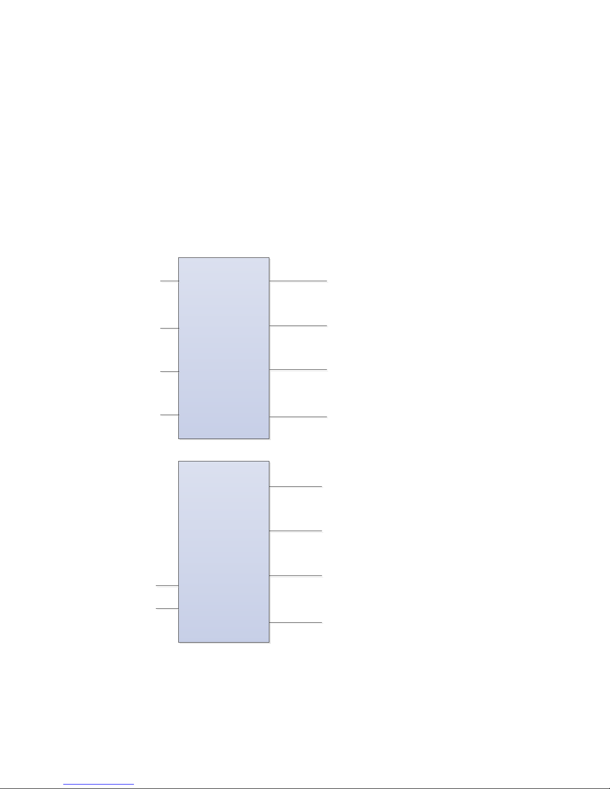
3.17 Parallella On-Board Power Management
The on-board power rails are regulated by the Intersil PMICs ISL9307 and ISL9305 as shown in the
following Figure.
Figure 5: Power Management
REV 14.09.09 19
Page 20

All four voltage rail outputs on the ISL9305 can be set by programming the appropriate registers within
the chip using the I2C interface. The Parallella on-board flash contains the appropriate programming
sequence to set the VDD_DSP rail to 1.0V and the VDD_GPIO rail to 2.5V automatically at boot time.
3.18 Parallella Supply Outputs
The Parallella can power expansion/daughter cards directly using the PEC_POWER connector.
The following voltages are available at the PEC_POWER connector:
• 5V
• 3.3V
• 2.5V
• VADJ
• VAD_GPIO
• 1.8V
• 1.35V
• 1.0V (Zynq)
• 1.0V (Epiphany)
The two on-board PMICs can deliver 1.5A on each step-down converter output and 300MA on each
general purpose LDO output. The amount of current drawn by the Parallella board will depend on the
level of activity on the board and the amount of current left over for the expansion card is yet to be
characterized.
NOTE: At this time, the PEC_POWER feature should be considered experimental. The safest power
solution for expansion cards is to: 1.) Have a completely independent power sub system or 2.) To use the
5V PEC_POWER rail.
Each one of the Parallella rails can also be powered directly from the PEC_POWER connector instead of
from the on board power management ICs. Each rail to be driven from an external connector would first
need to be powered down appropriately to avoid damaging the circuitry. To disable one of the ISL7307
outputs, pull down the corresponding REG_EN* signal available on the PEC_POWER connector. To disable
one of the ISL9305 outputs, program the appropriate registers using the I2C interface.
NOTE: There WILL be permanent damage to the board the power rails are driven incorrectly. Please
exercise extreme caution!
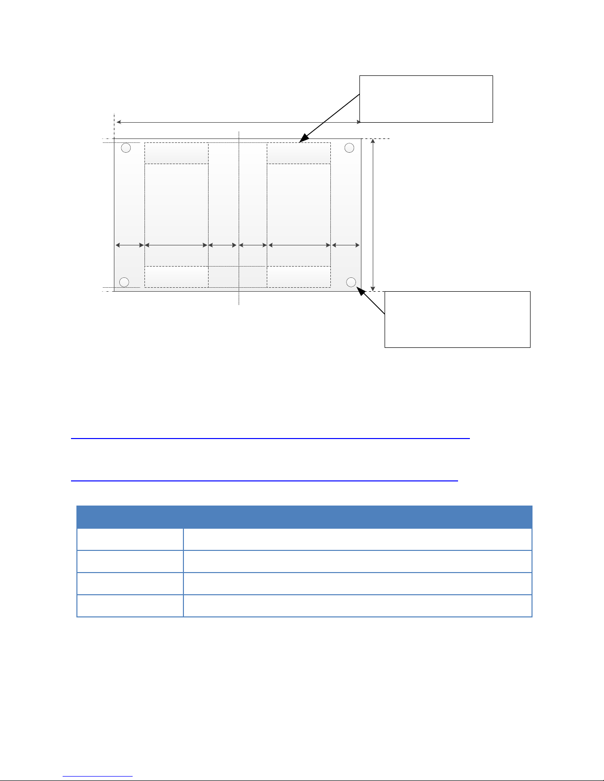
3.19 Parallella Expansion Connectors
The Parallella board has four expansions connectors placed on the opposite edges of the bottom side of
the board shown in Figure 2. For exact connector and placement information, please refer to the Parallella
mechanical drawings. The following figure shows the expansion connector placements as seen from the
bottom side of the board.
REV 14.09.09 20
Page 21
2
.150"
3.275"
Center
Line
0.045"
0.045"
0.43"
0
.840"0.43"
PEC_NORTH
PEC_SOUTH
0.840" 0.43"
PEC_GPIO
PEC_POWER
0.43"
0.045"
4 MOUNTING HOLES:
• 0.125" from edge to hole
center in X and Y direction
• 0.125" hole diameter
4 PEC CONNECTORS (BACK) :
• 0.045" from long edge
• 0.43" from short edge
TOP SIDE
The Parallella Expansion Connectors uses the 60 pin BSH-030-01-FDA high speed connector from Samtec.
The corresponding mating connector to be placed on the expansion card is BTH-030-01-FDA. The
complete data sheets can be found at:
https://www.samtec.com/technical-specifications/Default.aspx?SeriesMaster=BSH
A complete characterization report for the Samtec connectors can be found at:
http://www.samtec.com/Documents/WebFiles/TestRpt/172630_report_rev_2_qua.pdf
Connector Functions
PEC_POWER Power and control signal expansion connector
PEC_FPGA Zynq programmable logic expansion connector
PEC_NORTH Epiphany north link expansion connector
PEC_SOUTH Epiphany south link expansion connector
The four symmetrically placed connectors allow for robust mating of expansion cards and the Parallella
board using matching BTH-030-01-FDA connectors. As shown in Figure 5, it is possible to connect a single
full length credit card sized expansion cards or two half-length expansion cards. The left side shows two
half-length expansion boards (pink/green transparent) connected to the backside of the Parallella board
REV 14.09.09 21
Figure 6: PEC Placement Diagram
Figure 7: Parallella Expansion Connectors (PEC)
Page 22
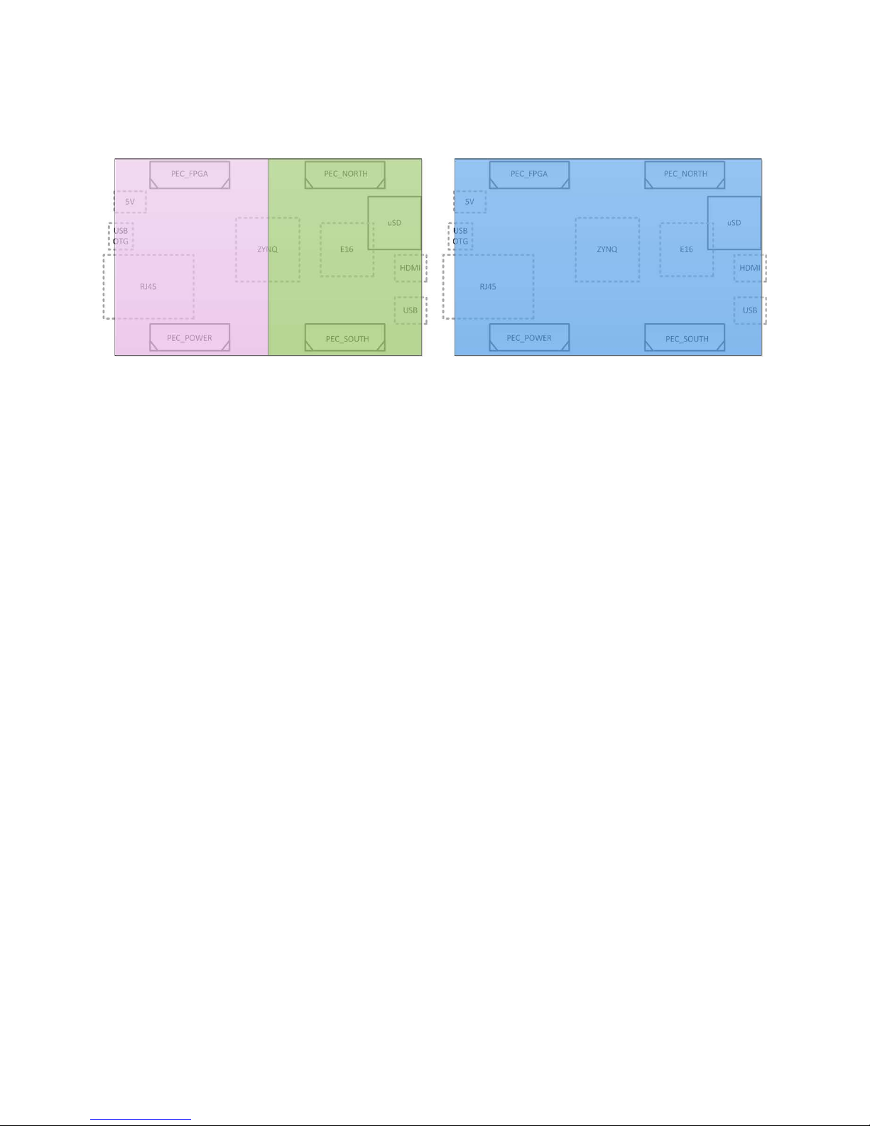
and the right side shows a full length (blue transparent) expansion board connected to the backside of
the Parallella board.
Figure 8: Daughter Card Configurations
3.20 Mounting Holes
The board has four symmetrically placed mounting holes, one in each corner. The mounting holes have a
diameter of 0.125”.
Three of the mounting holes are connected to ground while the fourth mounting hole is floating by
default. This floating mounting hole can be connected to the 5V supply as a build or solder option, allowing
power to be easily applied to a stack of Parallella boards without the need for extensive 5V DC cabling.
REV 14.09.09 22
Page 23

4 Parallella System Architecture
4.1 Zynq Memory Map
The following Table shows the hard-coded memory architecture of the Zynq architecture most relevant
to the Parallella architecture. For a complete description of the Zynq of the memory architecture, please
refer to the Architecture Reference manual for the Zynq.
Address Start Address
Size Function Note
End
0x0010_0000 0x3FFF_FFFF 1GB DRAM Accessible to all interconnect masters
0x4000_0000 0x7FFF_FFFF 1GB PL Custom logic address range
0x8000_0000 0xBFFF_FFFF 1GB PL Epiphany address range
0xFC00_0000 0xFCFF_FFFF 16MB FLASH Quad-SPI linear address for linear mode
0xFFFC_0000 0xFFFF_FFFF 252KB OCM OCM upper address range
Figure 9: Zynq Memory Map
The ARM communicates with programmable logic, GPIO connected to the programmable logic, and the
Epiphany by accessing the memory ranges shown in the table.
The Epiphany 32-bit memory space is mapped into the Zynq memory space allowing for easy sharing of
data and resources between the ARM and the Epiphany. The Epiphany address range is a matter of
convention and depends on the appropriate AXI master and slave interfaces being implemented within
the programmable logic on the Zynq.
REV 14.09.09 23
Page 24

4.2 Epiphany Memory Map
The Epiphany chip is situated within a 1GB section within the Zynq host processor memory map. The offset
within the 1GB space occupied by an Epiphany coprocessor is set by the ROWID and COLID pins on the
Epiphany chip. The ROWID and COLID can be individually set on boards through the PEC_POWER
connector enabling direct board to board connection through the PEC_NORTH and PEC_SOUTH
connectors.
By default the address locations of the Epiphany cores on Parallella-16 are as shown in the
Table below.
Core Number Start Address End Address Size
(32,8) 80800000 80807FFF 32KB
(32,9) 80900000 80907FFF 32KB
(32,10) 80A00000 80A07FFF 32KB
(32,11) 80B00000 80B07FFF 32KB
(33,8) 84800000 84807FFF 32KB
(33,9) 84900000 84907FFF 32KB
(33,10) 84A00000 84A07FFF 32KB
(33,11) 84B00000 84B07FFF 32KB
(34,8) 88800000 88807FFF 32KB
(34,9) 88900000 88907FFF 32KB
(34,10) 88A00000 88A07FFF 32KB
(34,11) 88B00000 88B07FFF 32KB
(35,8) 8C800000 8C807FFF 32KB
(35,9) 8C900000 8C907FFF 32KB
(35,10) 8CA00000 8CA07FFF 32KB
(35,11) 8CB00000 9CB07FFF 32KB
Figure 10: Epiphany Memory Map
REV 14.09.09 24
Page 25
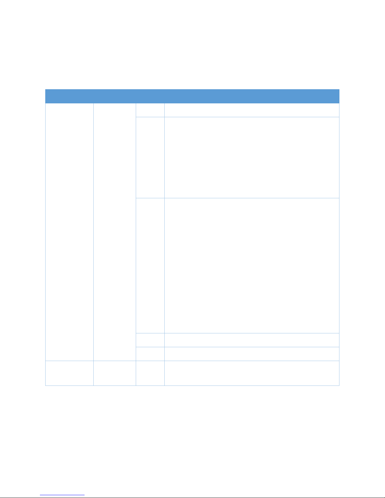
4.3 Epiphany Specific FPGA Resources
Developers that want leverage the Epiphany co-processors should use the Parallella programmable logic
reference design with minimal changes for best results. The following registers must be accessible by the
Epiphany drivers from the ARM for correct operation.
Register Address Bits Details
ESYSCONFIG 0x808f0f00 [0] Enable transaction timeout on read from Zynq
[2:1] 00: Filter disable
01: Inclusive range. Block transactions inside
REG_FILTERL and REG_FILTERH range)
10: Exclusive range. Block transactions outside
REG_FILTERL and REG_FILTERH range)
11: Reserved
[3] Epiphany eLink enable
0:
1.) Forces RESET_N to zero,
2.) turns off the epiphany input clock cclk
3.) and turns off the elink TX/RX in the FPGA
1:
1.) Turns on epiphany clock,
2.) forces RESET_N to one (“out of reset”)
3.) Turns on elink RX/TX in the FPGA
[27:4] Reserved
[31:28] Epiphany transaction control mode
ESYSRESET 0x808f0f04 A write transaction to this register asserts a reset signal to
Epiphany and the eLink logic within the Zynq.
REV 14.09.09 25
Page 26

ESYSINFO 0x808f0f08 [7:0] Platform #:
0=undefined
1=parallella-1.x,e16,7z020,gpio
2=parallella-1.x,e16,7z020,no-gpio
3=parallella-1.x,e16,7z010,gpio
4=parallella-1.x,e16,7z010,no-gpio
5=parallella-1.x,e64,7x020,gpio
[15:8] FPGA load type #:
0=undefined
1=hdmi enabled, gpio unused
2=headless, gpio unused
[23:16] Revision #:
0=undefined
1=first version
2=second version
3=etc..
ESYSFILTERL 0x808f0f0c [31:0] 32-bit Transaction Filter (Low), [1:0] are ignored
ESYSFILTERH 0x808f0f10 [31:0] 32-bit Transaction Filter (High), [1:0] are ignored
ESYSFILTERC 0x808f0f14 [31:2] Captured address of a filter violation
[1:0] Filter capture status
00 - not a valid value
01 - First violating transaction
10 - Second violating transaction
11 - There are more than 3 violating transactions
A write to this register clears value to zero
Table 4: Epiphany System Registers
The Epiphany coprocessor is connected to the Zynq SOC via the 48-pin eLink interface. An Epiphany eLink
protocol is implemented in the programmable logic portion of the Zynq SOC. In addition to the eLink
interface, the programmable logic within the Parallella board includes an AXI master interface, an AXI
slave interface, and an optional HDMI controller interface.
REV 14.09.09 26
Page 27
5 Board Configuration
5.1 FPGA Pin Assignment
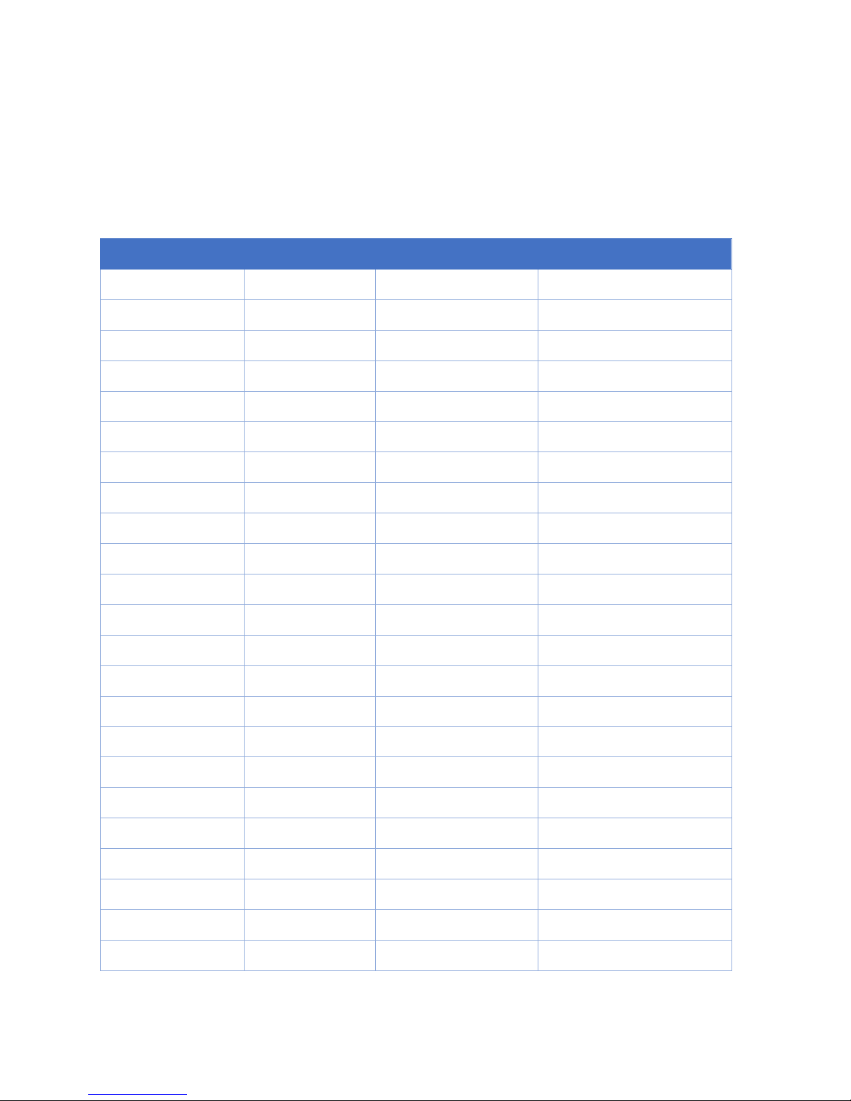
The following table shows the pin assignment of the programmable logic within the Zynq FPGA. A text
version of this table “UCF file”, can be found at:
Net Name Zynq Pin Direction IOSTANDARD
HDMI_D8 Y18 output LVCMOS25
HDMI_D9 W18 output LVCMOS25
HDMI_D10 V18 output LVCMOS25
HDMI_D11 V15 output LVCMOS25
HDMI_D12 R18 output LVCMOS25
HDMI_D13 P18 output LVCMOS25
HDMI_D14 Y19 output LVCMOS25
HDMI_D15 W19 output LVCMOS25
HDMI_D16 W15 output LVCMOS25
HDMI_D17 T19 output LVCMOS25
HDMI_D18 R19 output LVCMOS25
HDMI_D19 P19 output LVCMOS25
HDMI_D20 W20 output LVCMOS25
HDMI_D21 V20 output LVCMOS25
HDMI_D22 U20 output LVCMOS25
HDMI_D23 T20 output LVCMOS25
HDMI_CLK R17 output LVCMOS25
HDMI_VSYNC V17 output LVCMOS25
HDMI_HSYNC T17 output LVCMOS25
HDMI_DE Y17 output LVCMOS25
SPDIF Y16 output LVCMOS25
HDMI_INT P20 input LVCMOS25
PS_I2C_SCL N18 inout LVCMOS25
REV 14.09.09 27
Page 28

PS_I2C_SDA N17 inout LVCMOS25
PROG_IO N20 inout LVCMOS25
TURBO_MODE R16 input LVCMOS25
GPIO0_P T16 inout LVDS_25
GPIO0_N U17 inout LVDS_25
GPIO1_P V16 inout LVDS_25
GPIO1_N W16 inout LVDS_25
GPIO2_P P15 inout LVDS_25
GPIO2_N P16 inout LVDS_25
GPIO3_P U18 inout LVDS_25
GPIO3_N U19 inout LVDS_25
GPIO4_P P14 inout LVDS_25
GPIO4_N R14 inout LVDS_25
GPIO5_P T14 inout LVDS_25
GPIO5_N T15 inout LVDS_25
GPIO6_P U14 inout LVDS_25
GPIO6_N U15 inout LVDS_25
GPIO7_P W14 inout LVDS_25
GPIO7_N Y14 inout LVDS_25
GPIO8_P U13 inout LVDS_25
GPIO8_N V13 inout LVDS_25
GPIO9_P V12 inout LVDS_25
GPIO9_N W13 inout LVDS_25
GPIO10_P T12 inout LVDS_25
GPIO10_N U12 inout LVDS_25
GPIO11_P T11 inout LVDS_25
GPIO11_N T10 inout LVDS_25
REV 14.09.09 28
Table 5: Zynq Bank32 Pin Assignments
Page 29

Net Name Zynq Pin Direction IOSTANDARD
RXI_CCLK_P H16 output LVDS_25
RXI_CCLK_N H17 output LVDS_25
DSP_RESET_N G14 output LVCMOS25
RXI_LCLK_P F16 output LVDS_25
RXI_LCLK_N F17 output LVDS_25
RXI_DATA0_P B19 output LVDS_25
RXI_DATA0_N A20 output LVDS_25
RXI_DATA1_P C20 output LVDS_25
RXI_DATA1_N B20 output LVDS_25
RXI_DATA2_P D19 output LVDS_25
RXI_DATA2_N D20 output LVDS_25
RXI_DATA3_P E18 output LVDS_25
RXI_DATA3_N E19 output LVDS_25
RXI_DATA4_P E17 output LVDS_25
RXI_DATA4_N D18 output LVDS_25
RXI_DATA5_P F19 output LVDS_25
RXI_DATA5_N F20 output LVDS_25
RXI_DATA6_P G17 output LVDS_25
RXI_DATA6_N G18 output LVDS_25
RXI_DATA7_P G19 output LVDS_25
RXI_DATA7_N G20 output LVDS_25
RXI_FRAME_P H15 output LVDS_25
RXI_FRAME_N G15 output LVDS_25
RXO_RD_WAIT J15 input LVCMOS25
RXO_RD_WAIT_P J18 input LVCMOS25
RXO_WR_WAIT_N H18 input LVDS_25
TXO_LCLK_P K17 input LVDS_25
TXO_LCLK_N K18 input LVDS_25
REV 14.09.09 29
Page 30

TXO_DATA0_P K19 input LVDS_25
TXO_DATA0_N J19 input LVDS_25
TXO_DATA1_P L14 input LVDS_25
TXO_DATA1_N L15 input LVDS_25
TXO_DATA2_P L16 input LVDS_25
TXO_DATA2_N L17 input LVDS_25
TXO_DATA3_P M14 input LVDS_25
TXO_DATA3_N M15 input LVDS_25
TXO_DATA4_P L19 input LVDS_25
TXO_DATA4_N L20 input LVDS_25
TXO_DATA5_P M19 input LVDS_25
TXO_DATA5_N M20 input LVDS_25
TXO_DATA6_P M17 input LVDS_25
TXO_DATA6_N M18 input LVDS_25
TXO_DATA7_P N15 input LVDS_25
TXO_DATA7_N N16 input LVDS_25
TXO_FRAME_P J20 input LVDS_25
TXO_FRAME_N H20 input LVDS_25
TXI_RD_WAIT_N K14 output LVDS_25
TXI_RD_WAIT_N J14 output LVDS_25
TXI_WR_WAIT_P K16 output LVDS_25
TXI_WR_WAIT_N J16 output LVDS_25
Table 6: Zynq Bank 34 Pin Assignments
REV 14.09.09 30
Page 31

Net Name Zynq Pin Direction IOSTANDARD
GPIO12_P Y12 inout LVDS_25
GPIO12_N Y13 inout LVDS_25
GPIO13_P W11 inout LVDS_25
GPIO13_N Y11 inout LVDS_25
GPIO14_P V11 inout LVDS_25
GPIO14_N V10 inout LVDS_25
GPIO15_P T9 inout LVDS_25
GPIO15_N U10 inout LVDS_25
GPIO16_P W10 inout LVDS_25
GPIO16_N W9 inout LVDS_25
GPIO17_P U9 inout LVDS_25
GPIO17_N U8 inout LVDS_25
GPIO18_P W8 inout LVDS_25
GPIO18_N Y9 inout LVDS_25
GPIO19_P Y8 inout LVDS_25
GPIO19_N Y7 inout LVDS_25
GPIO20_P Y6 inout LVDS_25
GPIO20_N U7 inout LVDS_25
GPIO21_P V7 inout LVDS_25
GPIO21_N V6 inout LVDS_25
GPIO22_P W6 inout LVDS_25
GPIO22_N T5 inout LVDS_25
GPIO23_P U5 inout LVDS_25
Table 7: Zynq Bank 13 Pin Assignments
REV 14.09.09 31
Page 32

6 Booting the Parallella
REV 14.09.09 32
Page 33
pin header that selects between DC power and USB
and Ethernet PHY. Driven by 1.5A
Core voltage for Epiphany coprocessor. Driven by 1.5A
and DDR3L SDRAM. Driven by 1.5A
General purpose voltage shared by USB PHY, Ethernet PHY,
IO voltage for Zynq, HDMI, and flash chip. Driven by 300mA
7 Parallella Expansion Connector Details
7.1 PEC_POWER
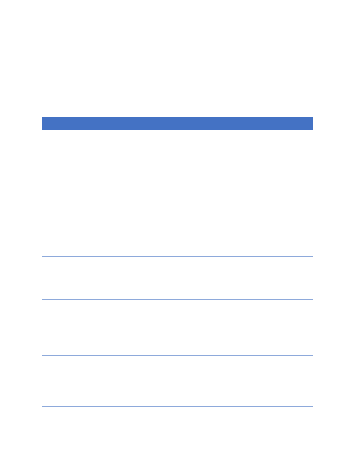
The PEC_POWER provides convenient access to various key Parallella board signals and can provide power
to expansion boards with modest current requirements. Expansion boards with substantial current
requirements should draw power from the SYS_5P0V connection or generate supply rails from a
completely independent DC supply.
Signal Direction Max Notes
SYS_5P0V Inout 5.0V Parallella expansion board supply. Driven by output of power
selector 3power.
1P0V Inout 1.0V Core voltage for Zynq
switching regulator output of PMIC.
VDD_DSP Inout 1.0V
switching regulator output of PMIC.
1P35V Inout 1.35V Supply shared by Zynq
switching regulator output of PMIC.
1P8V Inout 1.8V
Epiphany, Zynq, and HDMI. Driven by 1.5A switching regulator
output of PMIC.
2P5V Inout 2.5V IO voltage for Zynq LVDS interface that communicates with the
Epiphany coprocessor. Driven by 300mA LDO output of PMIC.
3.3V Inout 3.3V
LDO output of PMIC.
VDD_GPIO Inout 3.3V IO voltage for Zynq, HDMI, and flash chip. Driven by 300mA
LDO output of PMIC.
VDD_ADJ Inout 3.3V Independent supply output for expansion cards. Driven by
300mA LDO output on PMIC.
GND Inout 0.0V System Ground
I2C_SDA Inout 5.0V I2C bidirectional open-drain Serial Data Line
I2C_SCL Inout 5.0V I2C bidirectional open-drain Serial Clock Line
UART_TX Output 3.3V UART transmit signal
UART_RX Input 3.3V UART receive signal
REV 14.09.09 33
Page 34

PEC_NORTH/PEC_SOUTH to connect multiple Parallella
ems that utilize the
PEC_NORTH/PEC_SOUTH to connect multiple Parallella
SPDIF Output 2.5V Single bit SPDIF audio interface output
RESET_N Output 3.3V Active low Parallella board reset signal
USER_LED Output 3.3V On board LED signal driven by Zynq
DSP_XID[3:0] Input 1.8V Sets the relative chip column ID of the Epiphany chip on the
Parallella board, overriding the default board settings. These
signals must be driven correctly in systems that utilize the
boards.
DSP_YID[3:0] Input 1.8V Sets the relative chip row ID of the Epiphany chip on the
Parallella board, overriding the default board settings. These
signals must be driven correctly in syst
boards.
DSP_FLAG Output 1.8V Flag signal driven by the Epiphany.
TURBO_MODE Output 3.3V Not supported
JTAG_BOOT Input 3.3V Pull down to zero for JTAG boot
JTAG_TCK Input 3.3V JTAG Clock
JTAG_TMS Input 3.3V JTAG Test Mode
JTAG_TDI Input 3.3V JTAG Data Input
JTAG_TDO Output 3.3V JTAG Data Output
REG_EN1 Input 5V Drive low to disable on-board 1V regulator output
REG_EN2 Input 5V Drive low to disable on-board 1.8V regulator output
REG_EN3 Input 5V Drive low to disable on-board 3.3V regulator output
REG_EN4 Input 5V Drive low to disable on-board 2.5V regulator output
Table 8: PEC_POWER Signal Summary
REV 14.09.09 34
Page 35
Signal
SYS_5P0V
1
2
SYS_5P0V
I2C_SCL
3
4
I2C_SDA
REG_EN3
7
8
REG_EN3
DSP_XID[0]
13
14
DSP_YID[0]
DSP_XID[1]
15
16
DSP_YID[1]
DSP_XID[2]
17
18
DSP_YID[2]
DSP_XID[3]
19
20
DSP_YID[3]
DSP_FLAG
23
24
UART_RX
TURBO_MODE
25
26
UART_TX
JTAG_BOOT_EN
29
30
RESET_N
GND
31
32
GND
GND
35
36
GND
JTAG_TMS
37
38
JTAG_TDI
GND
41
42
GND
1P0V
43
44
1P0V
1P35V
47
48
1P35V
1P8V
49
50
1P8V
VDD_ADJ
53
54
VDD_ADJ
2P5V
57
58
2P5V
3P3V
59
60
3P3V
Pin Pin Signal
REG_EN1 5 6 REG_EN2
PROG_IO 9 10 NC
GND 11 12 GND
GND 21 22 GND
SPDIF 27 28 USER_LED
VADC_N 33 34 VADC_P
TAG_TCK 39 40 JTAG_TDO
VDD_DSP 45 46 VDD_DSP
GND 51 52 GND
VDD_GPIO 55 56 VDD_GPIO
Table 9: PEC_POWER Pin Mapping
REV 14.09.09 35
Page 36
Nominal voltage is 2.5V. The PMIC output voltage can be
7.2 PEC_FPGA
The PEC_FPGA can be used to connect the Zynq programmable logic to expansion cards or other
PEC_FPGA interfaces on another Parallella boards. The PEC_FPGA includes 48 bidirectional signals that
can be configured within the Zynq device to support a number of different signal standards, including
LVCMOS and LVDS.
Signal Direction Notes
VDD_GPIO Output Supply driven by power management IC on the Parallella board.
reprogrammed in software through I2C from the Zynq.
GND Inout System Ground
GPIOx_{N,P} Inout A differential pair or two single ended signals that connect between
an expansion card and the Zynq device on the Parallella board.
Table 10: PEC_FPGA Signal Summary
REV 14.09.09 36
Page 37
Signal
Pin
Pin
Signal
VDD_GPIO
1 2 VDD_GPIO
GPIO0_N
3 4 GPIO1_N
GPIO0_P
5 6 GPIO1_P
GPIO2_N
7 8 GPIO3_N
GPIO2_P
9
10
GPIO3_P
GND
11
12
GND
GPIO4_N
13
14
GPIO5_N
GPIO4_P
15
16
GPIO5_P
GPIO6_N
17
18
GPIO7_N
GPIO6_P
19
20
GPIO7_P
GND
21
22
GND
GPIO8_N
23
24
GPIO9_N
GPIO8_P
25
26
GPIO9_P
GPIO10_N
27
28
GPIO11_N
GPIO10_P
29
30
GPIO11_P
GND
31
32
GND
GPIO12_N
33
34
GPIO13_N
GPIO12_P
35
36
GPIO13_P
GPIO14_N
37
38
GPIO15_N
GPIO14_P
39
40
GPIO15_P
GND
41
42
GND
GPIO16_N
43
44
GPIO17_N
GPIO16_P
45
46
GPIO17_P
GPIO18_N
47
48
GPIO19_N
GPIO18_P
49
50
GPIO19_P
GND
51
52
GND
GPIO20 N
53
54
GPIO21 N
GPIO20_P
55
56
GPIO21_P
GPIO22_N
57
58
GPIO23_N
GPIO22_P
59
60
GPIO23_P
REV 14.09.09 37
Table 11: PEC_FPGA Pin Mapping
Page 38
1.8V supply driven by power management IC on the
back for transmitter indicating that device must
back for transmitter indicating that device must
back from receiver indicating that transmitter
transmitter indicating that transmitter
7.3 PEC_NORTH/PEC_SOUTH
The PEC_NORTH and PEC_SOUTH are connected to the north and south link of the Epiphany chip on the
Parallella board. These expansion connectors can be used to connect multiple Parallella boards in a
bidirectional line or ring configuration or they can be connected to an FPGA device that has Epiphany
eLink interface instantiated inside.
Signal Name Direction Signal Description
1P8V Output
Parallella board.
GND Inout System ground
RXI_{NO,SO}_DATA_{P,N}[7:0] Input Receiver data
RXI_{NO,SO}_FRAME_{P,N} Input Receiver packet framing signal
RXI_{NO,SO}_LCLK_{P,N} Input Receiver clock
RXO_{NO,SO}_WR_WAIT_{P,N} Output Push-
hold off on sending another write packet.
RXO_{NO,SO}_RD_WAIT_{P,N} Output Push-
hold off on sending another read packet.
TXO_{NO,SO}_DATA_{P,N}[7:0] Output Transmitter data
TXO_{NO,SO}_FRAME_{P,N} Output Transmitter packet framing signal
TXO_{NO,SO}_LCLK_{P,N} Output Transmitter clock
TXI_{NO,SO}_WR_WAIT_{P,N} Input Push-
must hold off on sending another write packet.
TXI_{NO,SO}_RD_WAIT_{P,N}
Input Push-back from
must hold off on sending another read packet.
Table 12: PEC_NORTH/SOUTH Signal Summary
REV 14.09.09 38
Page 39
Signal
Pin
Pin
Signal
1P8V
1 2 1P8V
RXI_NO_DATA_N[0]
3 4 RXI_NO_DATA_N[1]
RXI_NO_DATA_P[0]
5 6 RXI_NO_DATA_P[1]
RXI_NO_DATA_N[2]
7 8 RXI_NO_DATA_N[3]
RXI_NO_DATA_P[2]
9
10
RXI_NO_DATA_P[3]
GND
11
12
GND
RXI_NO_DATA_N[4]
13
14
RXI_NO_DATA_N[5]
RXI_NO_DATA_P[4]
15
16
RXI_NO_DATA_P[5]
RXI_NO_DATA_N[6]
17
18
RXI_NO_DATA_N[7]
RXI_NO_DATA_P[6]
19
20
RXI_NO_DATA_P[7]
GND
21
22
GND
RXI_NO_LCLK_N
23
24
RXI_NO_FRAME_N
RXI_NO_LCLK_P
25
26
RXI_NO_FRAME_P
RXO_NO_RD_WAIT_N
27
28
RXO_SO_WR_WAIT_N
RXO_NO_RD_WAIT_P
29
30
RXO_NO_WR_WAIT_P
GND
31
32
GND
TXO_NO_FRAME_N
33
34
TXI_NO_WR_WAIT_N
TXO_NO_FRAME_P
35
36
TXI_NO_WR_WAIT_P
TXO_NO_LCLK_N
37
38
TXI_NO_RD_WAIT_N
TXO_NO_LCLK_P
39
40
TXI_NO_RD_WAIT_P
GND
41
42
GND
TXO_NO_DATA_N[0]
43
44
TXO_NO_DATA_N[1]
TXO_NO_DATA_P[0]
45
46
TXO_NO_DATA_P[1]
TXO_NO_DATA_N[2]
47
48
TXO_NO_DATA_N[3]
TXO_NO_DATA_P[2]
49
50
TXO_NO_DATA_P[3]
GND
51
52
GND
TXO_NO_DATA_N[4]
53
54
TXO_NO_DATA_N[5]
TXO_NO_DATA_P[4]
55
56
TXO_NO_DATA_P[5]
TXO_NO_DATA_N[6]
57
58
TXO_NO_DATA_N[7]
TXO_NO_DATA_P[6]
59
60
TXO_NO_DATA_P[7]
Table 13: PEC_NORTH Pin Mapping for Parallella-16
REV 14.09.09 39
Page 40
Signal
Pin
Pin
Signal
1P8V
1 2 1P8V
TXO_NO_DATA_P[7]
3
4
TXO_NO_DATA_P[6]
TXO_NO_DATA_N[7]
5
6
TXO_NO_DATA_N[6]
TXO_NO_DATA_P[5]
7
8
TXO_NO_DATA_P[4]
TXO_NO_DATA_N[5]
9
10
TXO_NO_DATA_N[4]
GND
11
12
GND
TXO_NO_DATA_P[3]
13
14
TXO_NO_DATA_P[2]
TXO_NO_DATA_N[3]
15
16
TXO_NO_DATA_N[2]
TXO_NO_DATA_P[1]
17
18
TXO_NO_DATA_P[0]
TXO_NO_DATA_N[1]
19
20
TXO_NO_DATA_N[0]
GND
21
22
GND
TXO_NO_LCLK_P
23
24
TXI_NO_RD_WAIT_P
TXO_NO_LCLK_N
25
26
TXI_NO_RD_WAIT_N
RXO_NO_WR_WAIT_P
27
28
RXO_NO_RD_WAIT_P
RXO_NO_WR_WAIT_N
29
30
RXO_NO_RD_WAIT_N
GND
31
32
GND
TXO_NO_FRAME_P
33
34
TXI_NO_WR_WAIT_N
TXO_NO_FRAME_N
35
36
TXI_NO_WR_WAIT_P
RXI_NO_LCLK_P
37
38
RXI_NO_FRAME_P
RXI_NO_LCLK_N
39
40
RXI_NO_FRAME_N
GND
41
42
GND
RXI_NO_DATA_P[7]
43
44
RXI_NO_DATA_P[6]
RXI_NO_DATA_N[7]
45
46
RXI_NO_DATA_N[6]
RXI_NO_DATA_P[5]
47
48
RXI_NO_DATA_P[4]
RXI_NO_DATA_N[5]
49
50
RXI_NO_DATA_N[4]
GND
51
52
GND
RXI_NO_DATA_P[3]
53
54
RXI_NO_DATA_P[2]
RXI_NO_DATA_N[3]
55
56
RXI_NO_DATA_N[2]
RXI_NO_DATA_P[1]
57
58
RXI_NO_DATA_P[0]
RXI_NO_DATA_N[1]
59
60
RXI_NO_DATA_N[0]
Table 14: PEC_NORTH Pin Mapping for Parallella-64
REV 14.09.09 40
Page 41
Signal
Pin
Pin
Signal
1P8V
1 2 1P8V
RXI_SO_DATA_N[0]
3 4 RXI_SO_DATA_N[1]
RXI_SO_DATA_P[0]
5 6 RXI_SO_DATA_P[1]
RXI_SO_DATA_N[2]
7 8 RXI_SO_DATA_N[3]
RXI_SO_DATA_P[2]
9
10
RXI_SO_DATA_P[3]
GND
11
12
GND
RXI_SO_DATA_N[4]
13
14
RXI_SO_DATA_N[5]
RXI_SO_DATA_P[4]
15
16
RXI_SO_DATA_P[5]
RXI_SO_DATA_N[6]
17
18
RXI_SO_DATA_N[7]
RXI_SO_DATA_P[6]
19
20
RXI_SO_DATA_P[7]
GND
21
22
GND
RXI_SO_LCLK_N
23
24
RXI_SO_FRAME_N
RXI_SO_LCLK_P
25
26
RXI_SO_FRAME_P
RXO_SO_RD_WAIT_N
27
28
RXO_SO_WR_WAIT_N
RXO_SO_RD_WAIT_P
29
30
RXO_SO_WR_WAIT_P
GND
31
32
GND
TXO_SO_FRAME_N
33
34
TXI_SO_WR_WAIT_N
TXO_SO_FRAME_P
35
36
TXI_SO_WR_WAIT_P
TXO_SO_LCLK_N
37
38
TXI_SO_RD_WAIT_N
TXO_SO_LCLK_P
39
40
TXI_SO_RD_WAIT_P
GND
41
42
GND
TXO_SO_DATA_N[0]
43
44
TXO_SO_DATA_N[1]
TXO_SO_DATA_P[0]
45
46
TXO_SO_DATA_P[1]
TXO_SO_DATA_N[2]
47
48
TXO_SO_DATA_N[3]
TXO_SO_DATA_P[2]
49
50
TXO_SO_DATA_P[3]
GND
51
52
GND
TXO_SO_DATA_N[4]
53
54
TXO_SO_DATA_N[5]
TXO_SO_DATA_P[4]
55
56
TXO_SO_DATA_P[5]
TXO_SO_DATA_N[6]
57
58
TXO_SO_DATA_N[7]
TXO_SO_DATA_P[6]
59
60
TXO_SO_DATA_P[7]
Table 15: PEC_SOUTH Pin Mapping for Parallella-16
REV 14.09.09 41
Page 42
Signal
Pin
Pin
Signal
1P8V
1
2
1P8V
RXI SO DATA N[7]
3 4 RXI SO DATA N[6]
RXI SO DATA P[7]
5 6 RXI SO DATA P[6]
RXI SO DATA N[5]
7 8 RXI SO DATA N[4]
RXI SO DATA P[5]
9
10
RXI SO DATA P[4]
GND
11
12
GND
RXI SO DATA N[3]
13
14
RXI SO DATA N[2]
RXI SO DATA P[3]
15
16
RXI SO DATA P[2]
RXI SO DATA N[1]
17
18
RXI SO DATA N[0]
RXI SO DATA P[1]
19
20
RXI SO DATA P[0]
GND
21
22
GND
RXI SO LCLK N
23
24
RXO SO RD WAIT N
RXI SO LCLK P
25
26
RXO SO RD WAIT P
TXI SO WR WAIT N
27
28
TXI SO RD WAIT N
TXI SO WR WAIT P
29
30
TXI SO RD WAIT P
GND
31
32
GND
RXI SO FRAME N
33
34
RXO SO WR WAIT N
RXI SO FRAME P
35
36
RXO SO WR WAIT P
TXO SO LCLK N
37
38
TXOSOFRAMEN
TXO SO LCLK P
39
40
TXOSOFRAMEP
GND
41
42
GND
TXO SO DATA N[7]
43
44
TXO SO DATA N[6]
TXO SO DATA P[7]
45
46
TXO SO DATA P[6]
TXO SO DATA N[5]
47
48
TXO SO DATA N[4]
TXO SO DATA P[5]
49
50
TXO SO DATA P[3]
GND
51
52
GND
TXO SO DATA N[3]
53
54
TXO SO DATA N[2]
TXO SO DATA P[3]
55
56
TXO SO DATA P[2]
TXO SO DATA N[1]
57
58
TXO SO DATA N[0]
TXO SO DATA P[1]
59
60
TXO SO DATA P[0]
Table 16: PEC_SOUTH Pin Mapping for Parallella-64
REV 14.09.09 42
Page 43
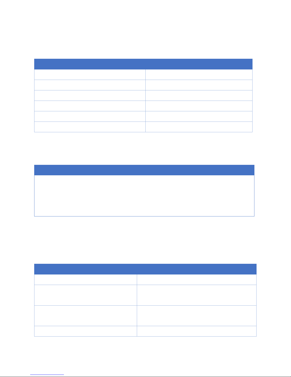
8 Electrical and Performance Specifications
8.1 Dimensions and Weight
Feature
Size 3.4’’ x 2.15’’
Height (with RJ45 and PECs) 1.25”
Height (without RJ45, PECs, 5V DC) 0.75”
PCB Layers 12
PCB Thickness 0.62’’
Weight 36 grams
Table 17: Dimensions and Weight
8.2 Power Consumption
The following table will contain the power consumption for typical Parallella use cases.
5V_IN 1P0V 1P8V 3P3V 2P5V VDD_DSP 1P35 VDD_ADJ VDD_GPIO
Idle TBD TBD TBD TBD TBD TBD TBD TBD TBD
Boot TBD TBD TBD TBD TBD TBD TBD TBD TBD
Nominal TBD TBD TBD TBD TBD TBD TBD TBD TBD
Max
TBD TBD TBD TBD TBD TBD TBD TBD TBD
Table 18: Power Consumption
8.3 Performance Metrics
The following table shows the performance specifications of the Parallella board at the time of publication
of this reference manual. Give more time for optimization and testing most of these metrics should
improve.
Performance Goal Value
Peak Zynq Frequency 667MHz
Peak Epiphany Instruction Issue Rate 19.2 GIPS (Parallella-16)
76 GIPS (Parallella-64)
Peak Epiphany Frequency 600 MHz (Parallella-16)
Peak Floating Point Performance 25 GFLOPS (Parallella-16)
REV 14.09.09 43
600 MHz (Parallella-64)
Page 44
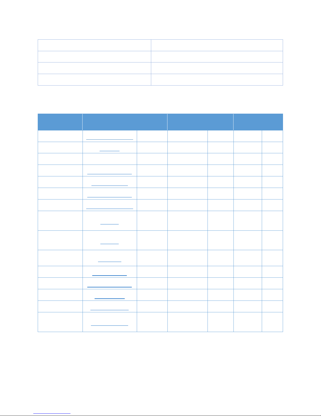
Device
Part Number
Power
Temp
Θ
ESD
Pb-
85 GFLOPS (Parallella-64)
Peak Bandwidth between Zynq and Epiphany 1.3GB/s
PEC_FPGA Peak Bandwidth 2.85GB/s (22.8 Gbps)
PEC_NORTH/PEC_SOUTH Peak Bandwidth 2.6GB/s (25.6 Gbps)
Table 19: Paralllella Performance Summary
8.4 IC Metrics Summary
JA
(W)
CPU Zynq™-7000 AP SoC 0.5 – 3 0 – 85° 19.0 1kV HBM Yes
Epiphany DSP E16G301 0.4 - 2 0 – 85° 22.6 n/a Yes
Eth PHY 88E1318 (n/a) 0.5 0 – 125° 37.5 n/a Yes
(C)
(0 m/s)
Free
USB PHY
HDMI PHY
SDRAM
Flash
PMIC #1
PMIC #2 ISL9305 0.2 - 1.5 0 – 125° 40.2
USB3320C-EZK-TR
ADV7513BSWZ
MT41K256M32SLD
N25Q128A13EF840E
ISL9307
0.1 0 – 85° n/a 8kV HBM Yes
0.3 0 – 85° 43 n/a Yes
0.9 0 – 95° (case) n/a n/a Yes
0.06 0 – 85° (amb) n/a 2kV HBM Yes
0.2 - 1.5 0 – 125° 40.2
3.5kV
HBM
3.5kV
HBM
Yes
Yes
Logic Buffer NC7WZ16 0.3* 0 – 125° 425 4kV HBM ???
Logic Buffer NC7SZ125M5X 0.15* 0 – 125° 425 n/a ???
Supply Monitor STM6904TWEDS6F ~0 0 – 85° 146 n/a Yes
LVDS Receiver SN65LVDS4R 0.04 0 – 85° (amb) 171 2kV HBM Yes
Clock Driver SI51219-A14BFT ~0 0 – 125° 181 4K HBM Yes
HDMI
Protection
TPD12S016PWR
~0 0 – 85° (amb) n/a 2K HBM Yes
REV 14.09.09 44
Table 20: IC Metrics
Page 45

9 About the Parallella Board
9.1 Design Information
The board is open source hardware and the Parallella project provides all the files required to study,
modify and manufacture the design.
The design resources provided include:
• Complete reference manual
• Schematic sources in OrCAD format
• PCB layout sources in Allegro format
• PCB manufacturing files in Gerber format
• Assembled board 3D CAD model(s)
• Bill of material
Design files for this board will be available at:
http://github.com/parallella/parallella-hw
9.2 Build Options
The following Parallella assembly options will be supported in manufacturing:
• Zynq Device: Z-7010 or Z-7020
• Epiphany Device: E16G301 or E64G401
• IO: With our without Samtec expansion connectors
• Display/USB: With or without HDMI and USB port
REV 14.09.09 45
Page 46

9.3 Contributors
• Adapteva: (http://www.adapteva.com)
o Parallella architecture and board design (Andreas Olofsson)
o Reference manuals (Andreas Olofsson)
o FPGA design (Roman Trogan, Fred Huettig)
o Linux distribution (Roman Trogan, Andreas Olofsson)
o Board bringup (Roman Trogan, Andreas Olofsson)
• Boston Design Solutions: (http://www.bostondesignsolutions.com/)
o Schematic and board layout (Mike Bakhtiari and Mike Damiano)
o Board bringup/debugging (Joe Galibois)
• Ant Micro: (http://www.antmicro.com/)
o HDMI bringup/debugging (Karol Gugala and Peter Gielda)
o Linux distribution (Karol Gugala)
• Community Review and Feedback:
o Andrew Back
o Flemming Christensen
o Gunnar Hillerström
o @trioflex
o @tschaboo
o @hamster
o @psupine
o @tnt
REV 14.09.09 46
Page 47
9.4 Attributions
Warranty notice and Disclaimers based on those found in the Beaglebone Black System Reference
Manual Rev A5.2, authored by Gerald Coley of Texas Instruments and published under the
Creative Commons Attribution Share-Alike 3.0 Unported License.
• The Parallella project benefited greatly from being able to study the design of the following open
source hardware projects:
o Arduino
o Beaglebone
• The Parallella project also drew inspiration from the following projects:
o Zedboard
o Raspberry Pi
9.5 Licensing
This work is licensed under the Creative Commons Attribution-Share Alike 3.0 Unported License. To view
a copy of this license, visit
http://creativecommons.org/licenses/bysa/3.0/
or Send a letter to Creative Commons, 171 Second Street, Suite 300, San Francisco, California, 94105, USA.
All derivative works are to be attributed to Adapteva.
Send all comments and errors concerning this document to [email protected]
REV 14.09.09 47
Page 48

9.6 Disclaimers
These design materials referred to in this document are *NOT SUPPORTED* and DO NOT constitute a
reference design. Only “community” support is allowed via resources at
http://forums.parallella.org
THERE IS NO WARRANTY FOR THE DESIGN MATERIALS DESCRIBED IN THIS REFERENCE MANUAL, TO THE
EXTENT PERMITTED BY APPLICABLE LAW. EXCEPT WHEN OTHERWISE STATED IN WRITING THE COPYRIGHT
HOLDERS AND/OR OTHER PARTIES PROVIDE THE DESIGN MATERIALS “AS IS” WITHOUT WARRANTY OF
ANY KIND, EITHER EXPRESSED OR IMPLIED, INCLUDING, BUT NOT LIMITED TO, THE IMPLIED WARRANTIES
OF MERCHANTABILITY AND FITNESS FOR A PARTICULAR PURPOSE. THE ENTIRE RISK AS TO THE QUALITY
AND PERFORMANCE OF THE DESIGN MATERIALS IS WITH YOU. SHOULD THE DESIGN MATERIALS PROVE
DEFECTIVE, YOU ASSUME THE COST OF ALL NECESSARY SERVICING, REPAIR OR
CORRECTION
This Parallella board was designed as an evaluation and development tool. It was not designed with any
other application in mind. As such, these design materials may or may not be suitable for any other
purposes. If used, the design material becomes your responsibility as to whether or not it meets your
specific needs or your specific applications and may require changes to meet your requirements.
For Feasibility Evaluation Only, in Laboratory/Development Environments: The Parallella Board is not a
complete product. It is intended solely for use for preliminary feasibility evaluation in
laboratory/development environments by technically qualified electronics experts who are familiar with
the dangers and application risks associated with handling electrical mechanical components, systems
and subsystems. It should not be used as all or part of a finished end product.
Your Sole Responsibility and Risk you acknowledge, represent, and agree that:
1. You have unique knowledge concerning Federal, State and local regulatory requirements (including but
not limited to Food and Drug Administration regulations, if applicable) which relate to your products and
which relate to your use (and/or that of your employees, affiliates, contractors or designees) of the
Parallella for evaluation, testing and other purposes.
2. You have full and exclusive responsibility to assure the safety and compliance of your products with all
such laws and other applicable regulatory requirements, and also to assure the safety of any activities to
be conducted by you and/or your employees, affiliates, contractors or designees, using the Parallella.
Further, you are responsible to assure that any interfaces (electronic and/or mechanical) between
the\Parallella and any human body are designed with suitable isolation and means to safely limit
accessible leakage currents to minimize the risk of electrical shock hazard.
3. Since the Parallella is not a completed product, it may not meet all applicable regulatory and safety
compliance standards which may normally be associated with similar items. You assume full responsibility
to determine and/or assure compliance with any such standards and related certifications as may be
applicable. You will employ reasonable safeguards to ensure that your use of the Parallella will not result
in any property damage, injury or death, even if the Parallella should fail to perform as described or
expected.
REV 14.09.09 48
Page 49

Certain Instructions: It is important to operate the Parallella within Supplier’s recommended
specifications and environmental considerations per the user guidelines. Exceeding the specified Parallella
ratings (including but not limited to input and output voltage, current, power, and environmental ranges)
may cause property damage, personal injury or death. If there are questions concerning these ratings
please contact the Supplier representative prior to connecting interface electronics including input power
and intended loads. Any loads applied outside of the specified output range may result in unintended
and/or inaccurate operation and/or possible permanent damage to the Parallella and/or interface
electronics. Please consult the System Reference Manual prior to connecting any load to the Parallella
output. If there is uncertainty as to the load specification, please contact the Supplier representative.
During normal operation, some circuit components may have case temperatures greater than 60 C as long
as the input and output are maintained at a normal ambient operating temperature. These components
include but are not limited to linear regulators, switching transistors, pass transistors, and current sense
resistors which can be identified using the Parallella schematic located at the link in the Parallella System
Reference Manual. When placing measurement probes near these devices during normal operation,
please be aware that these devices may be very warm to the touch. As with all electronic evaluation tools,
only qualified personnel knowledgeable in electronic measurement and diagnostics normally found in
development environments should use the Parallella.
Agreement to Defend, Indemnify and Hold Harmless: You agree to defend, indemnify and hold the
Suppliers, its licensors and their representatives harmless from and against any and all claims, damages,
losses, expenses, costs and liabilities (collectively, "Claims") arising out of or in connection with any use
of the Parallella that is not in accordance with the terms of the agreement. This obligation shall apply
whether Claims arise under law of tort or contract or any other legal theory, and even if the Parallella fails
to perform as described or expected.
Safety-Critical or Life-Critical Applications: If you intend to evaluate the components for possible use in
safety critical applications (such as life support) where a failure of the Supplier’s product would reasonably
be expected to cause severe personal injury or death, such as devices which are classified as FDA Class III
or similar classification, then you must specifically notify Suppliers of such intent and enter into a separate
Assurance and Indemnity Agreement.
REV 14.09.09 49
Page 50

9.7 Warranty
Parallella.org and Adapteva, Inc (Supplier) provide the Parallella board under the following conditions:
• The user assumes all responsibility and liability for proper and safe handling of the goods. Further,
the user indemnifies Supplier from all claims arising from the handling or use of the goods.
• Should the Parallella not meet the specifications indicated in the Parallella Reference Manual, the
Parallella may be returned within 90 days from the date of delivery to the distributor of purchase
for a full refund.
THE FOREGOING LIMITED WARRANTY IS THE EXCLUSIVE WARRANTY MADE BY SELLER TO BUYER AND IS
IN LIEU OF ALL OTHER WARRANTIES, EXPRESSED, IMPLIED, OR STATUTORY, INCLUDING ANY WARRANTY
OF MERCHANTABILITY OR FITNESS FOR ANY PARTICULAR PURPOSE. EXCEPT TO THE EXTENT OF THE
INDEMNITY SET FORTH ABOVE, NEITHER PARTY SHALL BE LIABLE TO THE OTHER FOR ANY INDIRECT,
SPECIAL, INCIDENTAL, OR CONSEQUENTIAL DAMAGES.
For up to date board information, please refer to:
http://github.com/parallella/parallella-hw
All support for this board is provided via community support at
http://forums.parallella.org
Before returning the board, please request an RMA at:
www.parallella.org/support/rma
Please DO NOT return the board without approval from the Parallella RMA team first. All boards received
without RMA approval will not be worked on.
REV 14.09.09 50
 Loading...