Page 1
599 Menlo Drive • # 100 • Rocklin, CA 95765
Sales / Technical Support - Tel: (916) 624-8333 Fax: (916) 624-8003
RF MODULES
433.92 MHz
433.92 MHz
433.92 MHz
Part # 27988
Part # 27986
Part # 27987
Compatible with:
Receiver
Part # 27987
Compatible with:
Transmitter
Transceiver
Part # 27986
Compatible with:
Transmitter
Part # 27986
Single Direction
Bi-Directional
Single Direction
TRANSMITTER
Send Only
Transceiver
Part # 27988
TRANSCEIVER
Send and Receive
Receiver
Part # 27987
RECEIVER
Receive Only
Transceiver
Part # 27988
GENERAL DESCRIPTION
There are three Wireless RF Modules, Transmitter, Receiver and a Transceiver. These RF Modules are
designed to serve as a tool for electronic design engineers, developers, hobbyists and students to perform
wireless experiments. These modules make it easy for any NON RF Experienced developer to add Wireless
RF Remote Control to their project. NO RF Knowledge required. The RF Modules are in a PCB (Printed Circuit
Board) form with a 17 Pin 0.1 Inch spacing header that fits directly into most all prototyping boards. They are
easy to use boards that include encoders, decoders, addressing, RF data processing and even the antenna, in
a simple fully range tested board, that is ready to plug right into your project. Just apply +5VDC, ground, and
the communication pins you require and enjoy hassle free wireless communications.
The Transmitter, Receiver and Transceiver all have 9600 baud serial interfaces and stand-alone, 3 function
switch inputs and outputs. The modules can communicate over distances up to 250 feet. The boards operate
on +5V and easily interface to your Basic Stamp 2 or Basic Stamp 2sx.
Web: http://www.parallaxinc.com or http://www.stampsinclass.com • Email: stamptech@parallaxinc.com
1-27-2000, V1.0 • Mfg. by www.RFDigital.com Page 1
Page 2
599 Menlo Drive • # 100 • Rocklin, CA 95765
Sales / Technical Support - Tel: (916) 624-8333 Fax: (916) 624-8003
RF MODULES
MINIMAL REQUIREMENTS
Two Modes of Operation:
Connecting GND to the Mode pin places the module in Switch Mode.
Connecting +5V to the Mode pin places the module in Serial Mode.
Switch Mode:
The transmitter, receiver and transceiver have 4 address pins (labeled ADDR1 – ADDR4), providing 16 address
combinations. Placing 0V or 5V on the 4 address pins sets the unit’s address (in a binary fashion). For
example, placing 0V on all pins sets the address to zero. Placing 5V on all pins sets the address to 15.
The transmitter, receiver and transceiver also have 3 switch data pins (labeled IN1 – IN3). 0V or 5V logic levels
placed on the input pins of the transmitting module are automatically sent to the output pins (labeled OUT1 –
OUT3) on the receive module. In addition, 16 different modules can be addressed with the built-in 4-bit address
pins. The receiver will receive the switch data on its 3 switch output pins only when its 4-bit address matches
the transmitter’s 4-bit address. The 4-bit address does not apply to serial mode.
Serial Mode
In serial mode (with +5V applied to the Mode pin) the modules can send and receive serial data at 9600, N, 8, 1
with +5V and 0V logic levels. Simply connect a single wire to the Transmit Data pin (labeled TXD) and send
9600 baud data into the module. The receive module outputs the same data at 9600 baud. All RF data
processing is done automatically by the modules. You cannot send a continuous 9600 baud stream; spacing
between 9600 baud bytes has to be at least 15 milliseconds. A flow control pin is provided for the transmitting
side to assist with achieving maximum efficient throughput. The Parallax Basic Stamp 2 and BASIC Stamp 2sx
have built-in commands to do serial byte pacing and flow-control handshaking in one single instruction (see
source code examples).
Single direction communication requires at least:
Option a: 1 Transmitter and 1 Receiver.
Option b: 1 Transmitter and 1 Transceiver.
Option c: 1 Transceiver and 1 Receiver.
Bi-directional communication requires at least: 2 Transceivers.
Multi Point Communications can be achieved by:
Placing one transmitter at each node that needs to send information.
Placing one receiver at each node that needs to receive information.
Placing one transceiver at each node that needs to send and receive information.
REGULATORY WARNINGS
These modules (boards) are not FCC approved. They are designed to comply with the FCC Part 15 Rules
and Regulations. They are not in a finished product form. They are strictly intended for experimental
purposes only. If you wish to use these modules in an actual product (a non-experimental capacity), the
module must first be designed into the product, then the whole product must be approved by the FCC. For a
list of FCC approved Labs that can test your final product for compliance contact RF Digital Corporation at
(818) 500-1082 or visit their web site at http://www.rfdigital.com.
Web: http://www.parallaxinc.com or http://www.stampsinclass.com • Email: stamptech@parallaxinc.com
1-27-2000, V1.0 • Mfg. by www.RFDigital.com Page 2
Page 3
599 Menlo Drive • # 100 • Rocklin, CA 95765
Sales / Technical Support - Tel: (916) 624-8333 Fax: (916) 624-8003
RF MODULES
It is the responsibility of the user to be aware of the regulatory requirements in their area of operation and
application. For exact information contact the FCC Office at:
Federal Communications Commission
445 12th St. SW
Washington DC 20554
(202) 418-0190
http://www.fcc.gov
USE OUTSIDE OF THE U.S.A. It is the responsibility of the user to be aware of the regulatory requirements
in their area of operation and application. Contact your local regulatory agency and obtain compliance
information.
For O.E.M. Design-In Guidance for the modules please contact:
RF Digital Corporation
1160 North Central Ave. Suite 201
Glendale, CA 91202
Tel: (818) 500-1082
Fax: (818) 246-9122
Web: www.rfdigital.com
Email: oem@rfdigital.com or info@rfdigital.com or support@rfdigital.com
OPERATION WARNINGS
Do not expose the boards to direct outdoor environment. If they will be used outdoors, keep them away from
water, moisture and direct sunlight.
The serial input and output pins operate at +5V and 0V logic levels. Do not attempt to connect directly to a
computer RS232 port as this will damage the module. Typical levels at a computer RS232 port are +10V
and -10V; these voltages would immediately damage the module. The module is intended to interface
directly with the Basic Stamp 2, the BASIC Stamp 2sx and other +5V logic devices.
Keep the top part of the board (PCB Trace Antenna, opposite end of the 17 pin header) at least 4 inches
away from any object, especially metal, wires and batteries as this will de-tune the antenna, drastically
reducing performance. Laying the module flat on a work desk made of wood, plastic or glass can sometimes
cause problems as well, since some paints contain conductive materials.
Do not touch the adjustable capacitor located at the top of the board. This part is factory tuned and must not
be adjusted. It is set at an optimal operating position and if moved will drastically reduce performance.
If mounting the board, use the mounting holes located in the center and corner of the boards. Only use
plastic stand-offs and plastic screws. Using any electrically conductive materials near the board will reduce
performance of the board.
Web: http://www.parallaxinc.com or http://www.stampsinclass.com • Email: stamptech@parallaxinc.com
1-27-2000, V1.0 • Mfg. by www.RFDigital.com Page 3
Page 4
599 Menlo Drive • # 100 • Rocklin, CA 95765
Sales / Technical Support - Tel: (916) 624-8333 Fax: (916) 624-8003
RF MODULES
SPECIFICATIONS
For best performance position the module boards as high off the ground as possible, in a horizontal position
and keep as far away from microprocessors (or wires connected to microprocessors) as possible. High
speed switching noise can interfere with reception.
In classroom environments, many transmitters and receivers may be within communication range. When not
in use, disconnect power from your project, including the module, to assure there is no chance for
unintentional transmission. Transmissions from other devices can disallow other students to perform their
wireless experiments.
Mechanical:
Size: 1.75 Inch x 3.25 Inch x 0.4 Inch
Environmental:
Temperature: +10c to +60c
Electrical:
Power: +5 VDC +/- 0.250 VDC
Logic Levels:
Cmos: 0V = Ground = Logic 0 = Logic Low
Cmos: +5V = VDD = Logic 1 = Logic High
Current Consumption:
Transmitter: 10 Milliamp (Condition: Transmitting in switched mode)
Receiver: 15 Milliamp (Condition: Receiving in switched mode, with no output load)
Transceiver: 20 Milliamp (Condition: Transmitting in switched mode)
Note: Loading output pins will add to current consumption.
Maximum Output Loading:
Maximum load per pin is 5 milliamps.
Maximum pin loading total: 15 milliamps.
RF:
Frequency: 433.92 MHz +/- 200 KHz Typical
Transmit: Typical 1 Milliwatt
Receive: Typical -104 dbm
Can drive a single led per output pin, in switched mode with a 470 ohm resistor in series. If it is needed to drive
larger loads, use NPN switching transistors.
Absolute Maximum Voltage On Any Pin: +5.25 VDC, -0.250 VDC
Web: http://www.parallaxinc.com or http://www.stampsinclass.com • Email: stamptech@parallaxinc.com
1-27-2000, V1.0 • Mfg. by www.RFDigital.com Page 4
Page 5

599 Menlo Drive • # 100 • Rocklin, CA 95765
Sales / Technical Support - Tel: (916) 624-8333 Fax: (916) 624-8003
RF MODULES
PIN DESCRIPTION
PIN 1: GND: (Input) Ground pin. Connect to power supply ground.
PIN 2: +5VDC: (Input) Power Supply pin. Connect to regulated +5VDC, +/- 0.250 VDC.
PIN 3: MODE: (Input) Serial/Switch Mode Pin. The Mode Pin, determines if module will operate in switch
mode or in serial mode. This pin has an internal pull down; leaving it open will be same as connecting it to
ground. This pin can be left open if only switch mode is to be used. Switch mode = 0VDC, Ground, Low, Logic
0, Open. Serial mode = 5VDC, High, Logic 1. Changes on this pin can take up to 1 second to take effect. This
pin can be changed on the fly, while power is applied.
PIN 4: TXD: (Input) Serial TX Data Input Pin. This pin is used to enter serial data for the transmitter to send.
Serial data should be sent at 9600 Baud, 8 Data Bits, No Parity, 1 Stop Bit. Standard Serial Protocol.
CAUTION: THIS IS NOT RS232! The module’s levels are +5VDC and ground (CMOS logic levels). RS232
levels exceed +10V and -10V, levels which will damage the module. If connection to an RS232 port is desired,
special circuitry is required to protect the input to the module. Continuous 9600 baud data cannot be input to this
pin, at least 15 millisecond spacing must be provided between the bytes. This pin only functions in Serial Mode.
PIN 5: TXFLO: (Output) Serial Flow Control Pin. This pin is used to achieve maximum serial throughput. The
module accepts data at 9600 baud but can only transmit between modules at 1200 baud. This pin is optional,
but can be used to automatically pace the data for maximum efficiency. This pin should connect to the device
that outputs the 9600 baud serial data to the module. When the module is ready to accept a 9600 baud byte,
this pin will be low. When the module is not ready to accept a 9600 baud byte, this pin will be high. The sending
device should monitor this pin to know exactly when the module is ready accept another byte for maximum data
transfer efficiency. The BASIC Stamp 2 and BASIC Stamp 2sx has a built-in flow-control pin feature in the
SEROUT command that works perfectly with the TXFLO pin. This pin only functions in Serial Mode.
PIN 6: RXD: (Output) Serial Receive Data Pin. This pin outputs serial data that is received by the receiver.
Serial data rate is 9600 Baud, 8 Data Bits, No Parity, 1 Stop Bit. Standard Serial Protocol. CAUTION: THIS IS
NOT RS232, its levels are +5VDC and ground, CMOS logic levels. RS232 levels exceed +10V and -10V, levels
which will damage the module. If direct connection to an RS232 port is desired, special circuitry is required to
protect the input to the module. This pin only functions in Serial Mode.
PIN 7: NC: (Input) NO Connection. Leave this pin open. Do not ground or terminate.
PIN 8: IN1: (Input) Switch Input 1. Internally pulled down. When left open this pin is logic low. When
connected to +5VDC this pin is logic high. A logic high on this pin will send a "1" to the receive pin OUT1. This
pin only functions in Switch Mode.
PIN 9: IN2: (Input) Switch Input 2. Internally pulled down. When left open this pin is logic low. When
connected to +5VDC this pin is logic high. A logic high on this pin will send a "1" to the receive pin OUT2. This
pin only functions in Switch Mode.
Web: http://www.parallaxinc.com or http://www.stampsinclass.com • Email: stamptech@parallaxinc.com
1-27-2000, V1.0 • Mfg. by www.RFDigital.com Page 5
Page 6

599 Menlo Drive • # 100 • Rocklin, CA 95765
Sales / Technical Support - Tel: (916) 624-8333 Fax: (916) 624-8003
RF MODULES
SIMILAR COMMUNICATING MODES
Transmitter = Serial Mode
Receiver = Serial Mode
PIN 10: IN3: (Input) Switch Input 3. Internally pulled down. When left open this pin is logic low. When
connected to +5VDC this pin is logic high. A logic high on this pin will send a "1" to the receive pin OUT3. This
pin only functions in Switch Mode.
PIN 11: OUT1: (Output) Switch Output 1. Normally low. When transmitter IN1 is high, this pin will be high.
500 Milliseconds after IN1 on the transmitter is returned to low, this pin will return to a low state. The 4-bit
address on both transmitter and receiver must match for this output pin to go high. Leaving all 4 address pins
disconnected will effectively set the module to address 0. This pin only functions in Switch Mode.
PIN 12: OUT2: (Output) Switch Output 2. Normally low. When transmitter IN2 is high, this pin will be high.
500 Milliseconds after IN2 on the transmitter is returned to low, this pin will return to a low state. The 4-bit
address on both transmitter and receiver must match for this output pin to go high. Leaving all 4 address pins
disconnected will effectively set the module to address 0. This pin only functions in Switch Mode.
PIN 13: OUT3: (Output) Switch Output 3. Normally low. When transmitter IN3 is high, this pin will be high.
500 Milliseconds after IN3 on the transmitter is returned to low, this pin will return to a low state. The 4-bit
address on both transmitter and receiver must match for this output pin to go high. Leaving all 4 address pins
disconnected will effectively set the module to address 0. This pin only functions in Switch Mode.
PIN 14: ADDR1: (Input) Address Input 1. 1 of 4 address input pins. 16 different binary combinations applied
to ADDR1 through ADDR4 allow unique addressing of transmitter, receiver, and transceiver pairs. This input
has no effect when in serial mode (when Mode pin is connected to +5V). This pin only functions in Switch Mode.
PIN 15: ADDR2: (Input) Address Input 2. 1 of 4 address input pins. 16 different binary combinations applied
to ADDR1 through ADDR4 allow unique addressing of transmitter, receiver, and transceiver pairs. This input
has no effect when in serial mode (when Mode pin is connected to +5V). This pin only functions in Switch Mode.
PIN 16: ADDR3: (Input) Address Input 3. 1 of 4 address input pins. 16 different binary combinations applied
to ADDR1 through ADDR4 allow unique addressing of transmitter, receiver, and transceiver pairs. This input
has no effect when in serial mode (when Mode pin is connected to +5V). This pin only functions in Switch Mode.
PIN 17: ADDR4: (Input) Address Input 4. 1 of 4 address input pins. 16 different binary combinations applied
to ADDR1 through ADDR4 allow unique addressing of transmitter, receiver, and transceiver pairs. This input
has no effect when in serial mode (when Mode pin is connected to +5V). This pin only functions in Switch Mode.
Similar mode settings are when the transmitter and receiver have the same mode setting. For example the
transmitter is set to serial mode and the receiver is set to serial mode. The two tables below indicate how the
modules will function
9600, 8, N, 1 serial data into the TXD pin of the transmitter and 9600, 8, N, 1 serial data out of the receiver
RXD pin.
Web: http://www.parallaxinc.com or http://www.stampsinclass.com • Email: stamptech@parallaxinc.com
1-27-2000, V1.0 • Mfg. by www.RFDigital.com Page 6
Page 7
599 Menlo Drive • # 100 • Rocklin, CA 95765
Sales / Technical Support - Tel: (916) 624-8333 Fax: (916) 624-8003
RF MODULES
Transmitter = Switch Mode
Receiver = Serial Mode
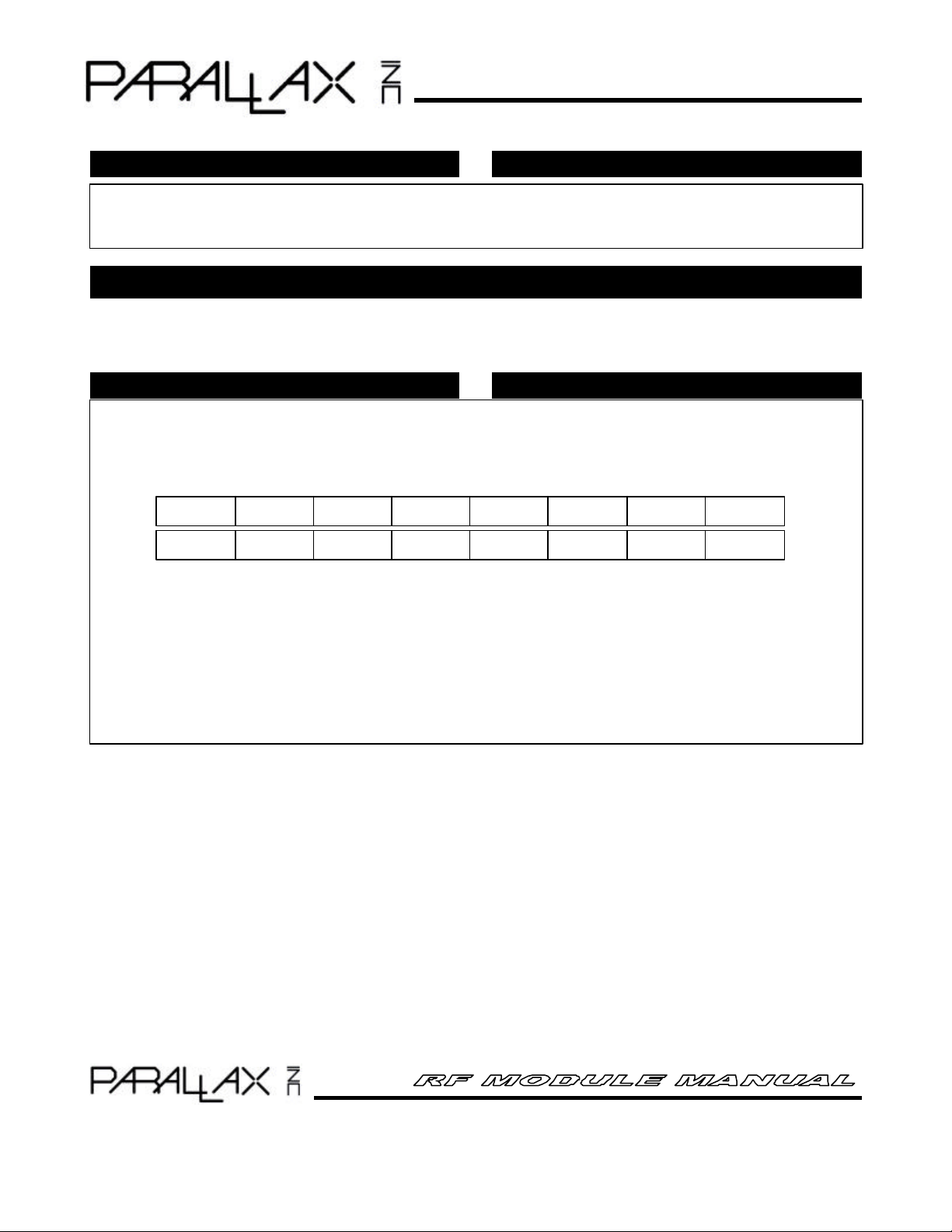
Any logic high (+5V) applied to IN1, IN2, or IN3 of the transmitter can be read out of the RXD serial output
OUT1
BIT 7
OUT2
BIT 6
OUT3
BIT 5
ADDR1
BIT 4
ADDR2
BIT 3
ADDR3
BIT 2
ADDR4
BIT 1
0
BIT 0
Transmitter = Switch Mode
Receiver = Switch Mode
Any logic high +5VDC placed on IN1, IN2 or IN3 of the transmitter will be reflected at the receiver’s OUT1,
match.
OUT2 or OUT3, respectively. Logic levels on transmitter and receiver address pins ADDR1 to ADDR4 must
NON-SIMILAR COMMUNICATING MODES
Non-similar mode settings are when the transmitter and receiver have opposite mode settings. For example,
transmitter’s Mode pin is connected to 0V (Switch Mode) and receiver’s Mode pin is connected to +5V (Serial
Mode)..
pin of the receiver. While any of the three inputs, IN1, IN2 or IN3 are high, the transmitter will repeatedly
df
transmit the same byte of information to the receiver. The byte contains IN1, IN2 and IN3 switch input
information, in addition to the status of the 4 address pins of the transmitter. See table below.
IMPORTANT: OUTPUT DATA BITS AND ADDRESS BITS ARE INVERTED
Example:
The transmitter is in switch mode and +5V is applied to ADDR3 and +5V is applied to IN1. With the receiver
in serial mode, the RXD pin will output the following serial byte; 01111100. The LSB, bit position "0" of the
received byte is not used and is always "0". For everywhere a "1" is placed on any transmitter input pin (IN1
– IN3) the receiver will display a "0" in that bit position. For everywhere a "0" or open is applied to any
transmitter input pin the receiver will display a "1" in that bit position. When a transmitter is in switch mode, it
will only transmit when one of the three inputs IN1, IN2 or IN3 are brought to +5V.
Web: http://www.parallaxinc.com or http://www.stampsinclass.com • Email: stamptech@parallaxinc.com
1-27-2000, V1.0 • Mfg. by www.RFDigital.com Page 7
Page 8

599 Menlo Drive • # 100 • Rocklin, CA 95765
Sales / Technical Support - Tel: (916) 624-8333 Fax: (916) 624-8003
RF MODULES
APPLICATIONS
Transmitter = Serial Mode
Receiver = Switch Mode
Serial data is input into the TXD pin of the transmitter at 9600, 8, N. Use the table below for addressing the
IN1
BIT 7
IN2
BIT 6
IN3
BIT 5
ADDR1
BIT 4
ADDR2
BIT 3
ADDR3
BIT 2
ADDR4
BIT 1
-
BIT 0
O.E.M. APPLICATIONS
receiver’s 4 address bits and the 3 OUT bits. When a serial byte is transmitted from the transmitter to the
receiver (with addresses), OUT1, OUT2 and OUT3 of the receiver will reflect the state of the bit positions in
transmitted byte. The receiver reads its address pins (ADDR1 through ADDR4) to verify the received byte is
intended for it. See table below.
IMPORTANT: INPUT DATA BITS AND ADDRESS BITS ARE INVERTED
Example:
The transmitter is in serial mode and the following byte is sent 10110110. The receiver will compare the
inverse of the 4 address bits to the settings on it's four address pins. If there is a match then it will enable it's
outputs and the first three MSB bits will be inverted and sent to the OUT1, OUT2 and OUT3 (OUT2 will be
high, OUT1 and OUT3 will be low). If the address does not match OUT1, OUT2 and OUT3 will not be
modified. For this example, the receiver (in switch mode) will need to have ADDR1= 0, ADDR2=1, ADDR3=0
and ADDR4=0. The LSB, BIT0, is a don't care bit. It can be 0 or 1 and the receiver will ignore this bit.
For O.E.M. Design-In Guidance for the modules please contact:
RF Digital Corporation
1160 North Central Ave. Suite 201
Glendale, CA 91202
Tel: (818) 500-1082
Fax: (818) 246-9122
Web: http://www.rfdigital.com
Email: oem@ rfdigital.com or info@rfdigital.com or support@rfdigital.com
Web: http://www.parallaxinc.com or http://www.stampsinclass.com • Email: stamptech@parallaxinc.com
1-27-2000, V1.0 • Mfg. by www.RFDigital.com Page 8
Page 9

599 Menlo Drive • # 100 • Rocklin, CA 95765
Sales / Technical Support - Tel: (916) 624-8333 Fax: (916) 624-8003
RF MODULES
Hook-up Using Switch Mode
The following example demonstrates an addressable, three-function pushbutton remote control. All inputs
including the mode pin are internally pulled low, so when in switch mode, it is not necessary to connect the mode
pin. Connecting the mode pin to ground or leaving it open has the same result. The LEDs on the receiver side
can be replaced with NPN transistors to be able to drive relays that can be used to switch high current loads. Do
not exceed 5 milliamps load for each output. The address switch settings on both transmit and receive side must
match.
Web: http://www.parallaxinc.com or http://www.stampsinclass.com • Email: stamptech@parallaxinc.com
1-27-2000, V1.0 • Mfg. by www.RFDigital.com Page 9
Page 10
599 Menlo Drive • # 100 • Rocklin, CA 95765
Sales / Technical Support - Tel: (916) 624-8333 Fax: (916) 624-8003
RF MODULES
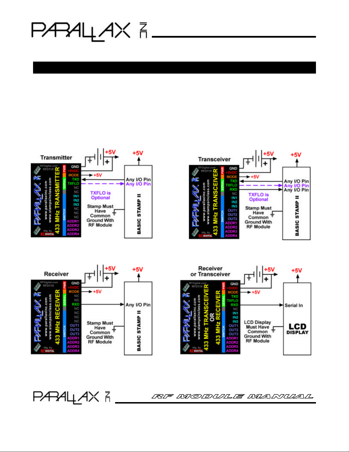
Hook-up Using Serial Mode
Use the Basic Stamp 2 or BASIC Stamp 2sx’s SERIN and SEROUT commands to send and receive 9600, N, 8,
1 bytes. The modules can not send and receive continuous 9600 baud serial data. If the Flow Control (TXFLO)
will not be used for sending serial data (TXD), you must have at least 15 milliseconds spacing between the start
of each byte. Refer to the SERIN and SEROUT commands in the Basic Stamp Manual for more information.
TXD, TXFLO and RXD pins are +5V logic. THEY DO NOT SUPPORT RS232 VOLTAGE LEVELS.
Do NOT connect directly to RS232 port.
Web: http://www.parallaxinc.com or http://www.stampsinclass.com • Email: stamptech@parallaxinc.com
1-27-2000, V1.0 • Mfg. by www.RFDigital.com Page 10
Page 11

599 Menlo Drive • # 100 • Rocklin, CA 95765
Sales / Technical Support - Tel: (916) 624-8333 Fax: (916) 624-8003
RF MODULES
BASIC STAMP 2 & BASIC STAMP 2SX - SAMPLE CODE
Visit our web site for code and documentation updates.
http://www.parallaxinc.com
Data can be sent and received with these modules simply by using the BASIC Stamp 2 and 2sx’s SERIN and
SEROUT commands (for Serial Mode) or simply by setting pins high and low (for Switch Mode). The RF
Transceiver, Transmitter and Receiver modules do an excellent job of filtering out background noise and provide
a clean serial stream or digital signal on the receiving side. Refer to the source code examples on the disk or CD
named Simple_Tx.BS2 and Simple_Rx.BS2 (for the BASIC Stamp 2), or Simple_Tx.BSX and Simple_Rx.BSX (for
the BASIC Stamp 2sx).
However, for nearly any kind of data transmission, the possibility of transceiving (the ability to transmit and
receive) is a very powerful thing. The bi-directional nature of this type of communication lends itself well to
sending data and verifying that it was received properly. This is of particular importance when the medium is one
that is typically prone to interference and dropout, such as with RF.
If you purchased the RF Transceivers (Part#27988) then you can take advantage of this capability to send and
receive data in a robust, error checking, fashion. The disk or CD that accompanies the RF Transceivers contains
a number of source code examples for interfacing the RF Transceivers to two BASIC Stamp 2 modules (or to two
BASIC Stamp 2sx modules) and communicating between them in a packet-type format. These examples focus
on a Master/Slave relationship. The Master device (one BASIC Stamp 2 with Transceiver) sends textual data
while the Slave device (the other BASIC Stamp 2 with Transceiver tries to receive the data properly and display it
on a 2 x 16 Serial LCD Module Part#27910 or 27913. Note: It is not required that you use this method to
send and receive data with these modules. The following information and examples are given as a means
of a very robust type of communication, if data accuracy is important to your application.
The Master and Slave devices actually carry out a bi-directional conversation over the RF Transceiver link to
send, receive, verify and re-send if necessary. The data sent from Master to Slave is formatted into a variablelength data packet. A data packet is simply some kind of data with a header and footer attached. The format for
the packets is shown in below:
Packet# Data Count Data Value 1 … Data Value n Checksum Checksum 2
BYTE 1 BYTE 2 BYTE n+1 BYTE n+2 BYTE n+3
Byte 1 consists of two pieces of data, the Packet Number and the Data Count. The Packet Number is a value
from 1 to 15 (0 is an illegal value). The Packet Number is the ID of the packet relative to the previously
transmitted packet and is used to verify that no duplicate packets are mistaken for new data. The Data Count is a
value from 0 to 15 representing the number of Data Values in this packet. Packets can contain from 1 to 16 bytes
of data values (at least 1 Data Value is required). Thus, the number of Data Values is actually Data Count + 1.
Byte 2 through Byte n+1 are the actual Data Values where n = Data Count + 1.
Byte n+2 and Byte n+3 marks the end of the packet and consists of a checksum value. Two different methods
are shown in the code examples. One simply XORs Byte 1 through Byte n+1 together to come up with a 1-byte
checksum (Byte n+2). This is a simple method but only catches about 90% of transmission errors and is
drastically affected by symmetrical data. (If this method is used, Byte n+2 is the last byte of the packet and Byte
Web: http://www.parallaxinc.com or http://www.stampsinclass.com • Email: stamptech@parallaxinc.com
1-27-2000, V1.0 • Mfg. by www.RFDigital.com Page 11
Page 12
599 Menlo Drive • # 100 • Rocklin, CA 95765
Sales / Technical Support - Tel: (916) 624-8333 Fax: (916) 624-8003
RF MODULES
n+3 doesn’t exist). The second method is based on a Cyclic-Redundancy-Check algorithm. The CRC16, as it is
called, uses a sophisticated equation to calculate a checksum that catches 99% of transmission errors and is
unaffected by symmetrical data. (If this method is used, Byte n+3 is the last byte of the packet).
The Master and Slave use an acknowledge-based protocol to communicate with each other. The process works
in the following fashion:
a) The Master decides to send some data.
i) It creates a new packet number (previous packet number + 1).
ii) It builds a packet, one byte at a time, calculating the checksum (using the XOR or the CRC method)
for each byte. It finishes the packet by appending the checksum (1 or 2 bytes) to the end.
iii) It transmits the entire packet.
b) The Slave periodically checks for incoming data.
i) If a packet arrives, it calculates a checksum (using the same method as the Master).
ii) If the calculated checksum matches the received checksum, the Slave transmits a positive
acknowledgement to the Master (by simply transmitting the checksum).
iii) If the calculated checksum does not match the received checksum, the Slave transmits a negative
acknowledgement to the Master (by simply transmitting the one’s-compliment form of the checksum).
iv) If the packet is good (as determined by step ii above) the Slave verifies that that packet number is not
the same as the previous packet’s (indicating that a duplicate was received) and processes the data
of the packet. In this example, the process is simply to pass the data on to the Serial LCD Display. If
the packet number is the same, the packet is just ignored.
v) If the packet is bad (as determined by step iii above), the Slave starts over, looking for a packet
again.
c) The Master, immediately after sending the packet, looks for an acknowledgement from the Slave.
i) If a negative acknowledgement or no acknowledgement was received, the Master delays a random
amount of time (0 to 255 ms) and then retransmits the entire packet.
ii) If a positive acknowledgement was received, the Master continues with its other tasks.
Using the above methods of transmission, data can be sent reliably for more than 250 feet. Our tests reached
more than 400 feet, with trees and buildings in between. Many packets became lost or damaged in transmission
but the two devices were able to adjust for this and communicate slowly. Your environment may cause different
results.
The source code provide is named “Txcvr_Master_…” and “Txcvr_Slave_…”. Each piece of code has a
corresponding companion program. For example, the Txcvr_Master_XOR.BS2 source code uses the XOR
method and is meant to be programmed into the “Master” device (a BASIC Stamp 2). The Slave device should
be programmed with the corresponding “Slave” code, namely Txcvr_Slave_XOR.BS2.
Be very careful to match up the correct code for the device and application. Do not try to program a BASIC
Stamp 2sx with code that ends in a .BS2 extension. Do not try to use the XOR code for the Master and the CRC
code for the Slave .
Web: http://www.parallaxinc.com or http://www.stampsinclass.com • Email: stamptech@parallaxinc.com
1-27-2000, V1.0 • Mfg. by www.RFDigital.com Page 12
 Loading...